JP2011527558A - Non-contact power receiving apparatus and operation method thereof - Google Patents
Non-contact power receiving apparatus and operation method thereof Download PDFInfo
- Publication number
- JP2011527558A JP2011527558A JP2011517373A JP2011517373A JP2011527558A JP 2011527558 A JP2011527558 A JP 2011527558A JP 2011517373 A JP2011517373 A JP 2011517373A JP 2011517373 A JP2011517373 A JP 2011517373A JP 2011527558 A JP2011527558 A JP 2011527558A
- Authority
- JP
- Japan
- Prior art keywords
- power receiving
- receiving device
- pickup coil
- tuning
- semiconductor switches
- Prior art date
- Legal status (The legal status is an assumption and is not a legal conclusion. Google has not performed a legal analysis and makes no representation as to the accuracy of the status listed.)
- Pending
Links
Images


Classifications
-
- H—ELECTRICITY
- H02—GENERATION; CONVERSION OR DISTRIBUTION OF ELECTRIC POWER
- H02J—CIRCUIT ARRANGEMENTS OR SYSTEMS FOR SUPPLYING OR DISTRIBUTING ELECTRIC POWER; SYSTEMS FOR STORING ELECTRIC ENERGY
- H02J50/00—Circuit arrangements or systems for wireless supply or distribution of electric power
- H02J50/10—Circuit arrangements or systems for wireless supply or distribution of electric power using inductive coupling
- H02J50/12—Circuit arrangements or systems for wireless supply or distribution of electric power using inductive coupling of the resonant type
-
- H—ELECTRICITY
- H02—GENERATION; CONVERSION OR DISTRIBUTION OF ELECTRIC POWER
- H02J—CIRCUIT ARRANGEMENTS OR SYSTEMS FOR SUPPLYING OR DISTRIBUTING ELECTRIC POWER; SYSTEMS FOR STORING ELECTRIC ENERGY
- H02J50/00—Circuit arrangements or systems for wireless supply or distribution of electric power
- H02J50/10—Circuit arrangements or systems for wireless supply or distribution of electric power using inductive coupling
Abstract
非接触受電装置は動的に同調が行われるピックアップコイルを備える。この受電装置の電力伝送能力は、その動作範囲の一部に亘って線形モードで動作する半導体スイッチを使用して動的に同調がなされる。半導体スイッチは、システムの要求仕様に応じて様々な制御手法を実行するように構成されている制御装置により駆動される。ピックアップコイルの動的な同調を行うために半導体スイッチを単独またはリアクタンス素子と共に使用してもよい。非接触受電装置は消費者向け電子デバイスまたは無線センサデバイスと共に使用してもよい。非接触受電装置を前記デバイスのエネルギー蓄積部品に組み込み、既存製品の改良に用いてもよい。そして、前記デバイスを充電パッドにより形成された平面磁界の近くに配置してもよい。 The non-contact power receiving apparatus includes a pickup coil that is dynamically tuned. The power transfer capability of the power receiving device is dynamically tuned using a semiconductor switch operating in a linear mode over a portion of its operating range. The semiconductor switch is driven by a control device configured to execute various control methods according to the required specifications of the system. A semiconductor switch may be used alone or with a reactance element to dynamically tune the pickup coil. The contactless power receiver may be used with a consumer electronic device or a wireless sensor device. A non-contact power receiving apparatus may be incorporated in the energy storage component of the device and used to improve existing products. The device may be disposed near a planar magnetic field formed by the charging pad.
Description
本発明は、誘導結合電力伝送システム(ICPT)の技術分野に関するものである。具体的には本発明は線形モードで動作する半導体スイッチを備えた非接触受電装置に関する。 The present invention relates to the technical field of inductively coupled power transfer systems (ICPT). Specifically, the present invention relates to a contactless power receiving device including a semiconductor switch that operates in a linear mode.
非接触電力システムは、電源から交流電流の供給を受ける導電経路を有する非接触送電装置と、一又は複数の非接触受電装置とを備えている。これらの非接触受電装置は導電経路の近傍に配置されるが、電気的には導電経路から絶縁されている。非接触受電装置は導電経路により形成される磁界によって電圧が誘起されるピックアップコイルを備え、電気負荷を提供するものである。通常、ピックアップコイルは、システムの電力伝送能力を高めるために同調コンデンサを用いて同調がなされる。 The non-contact power system includes a non-contact power transmission device having a conductive path that receives supply of alternating current from a power source, and one or a plurality of non-contact power reception devices. These non-contact power receiving devices are disposed in the vicinity of the conductive path, but are electrically insulated from the conductive path. The non-contact power receiving apparatus includes a pickup coil whose voltage is induced by a magnetic field formed by a conductive path, and provides an electric load. Typically, the pickup coil is tuned with a tuning capacitor to increase the power transfer capability of the system.
非接触受電装置における問題点の一つは、軽負荷時例えば受電装置から給電を受けるモータが制御システムからの指令待機中であり、停止している時に、効率が低下することである。これはピックアップコイルと負荷の間で、電力制御装置を介して電力の流れを制御することで解決可能である。 One of the problems in the non-contact power receiving device is that the efficiency decreases when the motor receiving power from the power receiving device is waiting for a command from the control system at a light load and is stopped. This can be solved by controlling the flow of power between the pickup coil and the load via a power control device.
電力制御装置として、ピックアップ回路の一部に短絡スイッチを用いること事により、適宜、ピックアップコイルを負荷から切り離すものがある。このような手法は、Auckland UniServices Limitedへ譲渡された米国特許5、293、308の明細書に「短絡制御」として記載されている。 Some power control devices use a short-circuit switch in a part of the pickup circuit to appropriately disconnect the pickup coil from the load. Such a technique is described as “short circuit control” in US Pat. No. 5,293,308 assigned to Auckland UniServices Limited.
上記に記載された技術は、ピックアップ側から負荷側への電力の流れ制御の問題については解決するものの、特に軽負荷時においては、ピックアップ回路がほぼ常に、無負荷または軽負荷の状態で短絡されるため、短絡スイッチにより大きな導電損失が発生する可能性がある。 Although the technique described above solves the problem of power flow control from the pickup side to the load side, the pickup circuit is almost always short-circuited in a no-load or light-load state, especially at light loads. Therefore, a large conductive loss may occur due to the short-circuit switch.
また、非接触電力システムにおける別の問題点として、負荷状態およびその他の回路パラメータの変化に起因する周波数変動がある。これによりピックアップコイルにおける誘起電圧の大きさおよび短絡回路の電流が変化し、システムの電力伝送能力に影響する可能性がある。これは固定的または受動的に同調がなされる非接触受電装置において特に問題となる。 Another problem in the non-contact power system is frequency fluctuations caused by changes in load conditions and other circuit parameters. As a result, the magnitude of the induced voltage in the pickup coil and the current in the short circuit change, which may affect the power transmission capability of the system. This is particularly a problem in contactless power receiving devices that are tuned either fixedly or passively.
米国特許明細書US2007/109708A1およびUS7、382、636B2に記載の手法では、受電装置の実効キャパシタンスまたは実効インダクタンスを変化させることによって電力ピックアップを動的に同調させまたは非同調としている。これにより非接触受電装置において、パラメータの変化に起因する周波数ドリフトの補償が可能になる。実効キャパシタンスまたは実効インダクタンスの変更は、コンデンサまたはコイルに直列接続された2つの半導体スイッチを用いて行う。更には可変コンデンサまたは可変抵抗のソフトスイッチングを実現するためにピックアップコイル電流の大きさおよび位相の検知手段が必要である。動的な同調を行うことにより、周波数ドリフトの補償のみならず、ピックアップコイルの共振周波数の微調整が可能になるため、受動的な同調システム(通常Q<6)と比較して、品質係数(Q>10)を大幅に増加させることができる。品質係数が高いとシステムの電力伝送能力を向上させる。 In the approach described in US patent specifications US2007 / 109708A1 and US7,382,636B2, the power pickup is dynamically tuned or untuned by changing the effective capacitance or effective inductance of the power receiving device. Thereby, in the non-contact power receiving apparatus, it is possible to compensate for the frequency drift caused by the parameter change. The effective capacitance or effective inductance is changed by using two semiconductor switches connected in series with a capacitor or a coil. Furthermore, a means for detecting the magnitude and phase of the pickup coil current is required to realize soft switching of the variable capacitor or variable resistor. Dynamic tuning allows not only compensation for frequency drift, but also fine tuning of the resonance frequency of the pickup coil, so compared to passive tuning systems (usually Q <6), the quality factor ( Q> 10) can be greatly increased. A high quality factor improves the power transfer capability of the system.
非接触電力ピックアップ回路の小型化を図る上では、高い周波数で特に複雑化するピックアップコイルセンサを省くとよい。ただし、これを省くことにより可変コンデンサまたは可変コイルをソフトスイッチすることができなくなる、即ち、システムがハードスイッチされるようになる。この手法は、スイッチング途中においてコイル電流が遮断され或いはコンデンサが短絡されるので、過大な電流または電圧を発生させる。その結果生じるスイッチング過度現象は、EMI、同調を行う半導体スイッチのストレスを引き起こすと共に過度の電力損失によりシステムの電力効率を低下させる。そして最悪の場合、システム障害が起きることもある。 In order to reduce the size of the non-contact power pickup circuit, it is preferable to omit a pickup coil sensor that is particularly complicated at a high frequency. However, if this is omitted, the variable capacitor or the variable coil cannot be soft-switched, that is, the system is hard-switched. This method generates excessive current or voltage because the coil current is cut off or the capacitor is short-circuited during switching. The resulting switching transients cause stress in the semiconductor switch that performs the EMI and tuning and reduce the power efficiency of the system due to excessive power loss. In the worst case, a system failure may occur.
本発明の目的は、既存のシステムの抱える一又は複数の問題点を改善する非接触受電装置の制御方法、または装置を提供する、若しくは少なくとも公共に有益な代替手段を提供することにある。 It is an object of the present invention to provide a control method or apparatus for a non-contact power receiving apparatus that improves one or more problems of existing systems, or at least to provide a publicly useful alternative.
本発明の一実施形態において提供する、非接触受電装置は以下を備える。
a.ピックアップコイル、
b.ピックアップコイルと回路を形成する一又は複数の半導体スイッチ、 および
c.前記非接触受電装置の出力に基づいて前記受電装置の同調を行うために、一又は複数の半導体スイッチを、少なくともその動作範囲の一部に亘って線形モードで駆動する制御回路。
A non-contact power receiving device provided in an embodiment of the present invention includes the following.
a. Pickup coil,
b. One or more semiconductor switches forming a circuit with the pickup coil; and c. A control circuit that drives one or more semiconductor switches in a linear mode over at least part of their operating range to tune the power receiving device based on the output of the non-contact power receiving device.
更なる実施形態において提供する、電子デバイスと共に使用するシステムは以下を備える。
a.磁界を形成するコイルに通電させる駆動回路を有する送電装置
b.上記記載の受電装置であって、電子デバイスに、エネルギー蓄積デバイスを介して、または直接接続された前記受電装置。。
A system for use with an electronic device provided in a further embodiment comprises:
a. A power transmission device having a drive circuit for energizing a coil forming a magnetic field; b. The power receiving apparatus as described above, wherein the power receiving apparatus is connected to an electronic device via an energy storage device or directly. .
更なる実施形態において提供する、送電装置によって磁界を介して受電装置のピックアップコイルに電力を送る非接触電力システムにおいて用いる方法であって、前記受電装置の少なくとも一部の動作範囲に亘って、前記受電装置のピックアップコイルに付与される抵抗を変化させることによって前記受電装置を同調する方法。 Provided in a further embodiment is a method for use in a non-contact power system for transmitting power to a pickup coil of a power receiving device via a magnetic field by a power transmitting device, the operation being performed over at least a part of the operating range of the power receiving device. A method of tuning the power receiving device by changing a resistance applied to a pickup coil of the power receiving device.
更なる実施形態において提供する、非接触受電装置は以下を備える。
a.ピックアップコイルの入力部、
b.前記ピックアップコイルの入力部に接続された一又は複数の半導体スイッチ、 および
c.前記ピックアップコイルの前記入力部に接続されて使用される制御回路であって、
前記非接触受電装置の出力に基づいて前記受電装置の同調を行うために、一又は複数の半導体スイッチを、少なくともその動作範囲の一部に亘って線形モードで駆動する制御回路。
A contactless power receiving device provided in a further embodiment includes the following.
a. Pickup coil input section,
b. One or more semiconductor switches connected to the input of the pickup coil; and c. A control circuit used by being connected to the input section of the pickup coil;
A control circuit that drives one or more semiconductor switches in a linear mode over at least part of their operating range to tune the power receiving device based on the output of the non-contact power receiving device.
付属の図面は明細書の一部を構成し、本発明の実施形態を図示するものであり、上記の発明の概要の説明および下記の実施形態の詳細な説明と共に発明の原理を説明する。
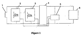
図1に一又は複数の半導体スイッチ2、3に接続されたピックアップコイル1を備えた非接触受電装置を示す。これらの半導体スイッチ2、3は、これら半導体スイッチ2、3を変調する制御回路5によって駆動される。図示の構成ではフルまたはハーフブリッジ整流回路4を備えることにより、直流を制御回路5および電子デバイスまたはエネルギー蓄積デバイス6へ供給している。
FIG. 1 shows a non-contact power receiving apparatus including a pickup coil 1 connected to one or a plurality of
磁界に近づくとピックアップコイル1に起電力が発生する。従来のトランスと比較して磁界とピックアップコイル1の磁気結合は非常に弱いため、通常、誘起電圧はそのまま使用するのには適さない。 When the magnetic field is approached, an electromotive force is generated in the pickup coil 1. Since the magnetic coupling between the magnetic field and the pickup coil 1 is very weak compared to a conventional transformer, the induced voltage is usually not suitable for use as it is.
電子デバイスまたはエネルギー蓄積デバイス6の所要電力に応じて電力を制御する電力制御装置が必要になる。また、システムの電力伝送能力を高めるためにはピックアップコイル1を同調させる必要がある。その際、動的な同調方法を用いて電力の制御、ピックアップコイル1の同調、ひいてはシステムの電力伝送能力を増減させてもよい。この補償法を用いることにより、更に非接触受電装置によるシステム周波数の変動に追従できるようになる。 A power control device that controls the power according to the required power of the electronic device or the energy storage device 6 is required. Further, in order to increase the power transmission capability of the system, it is necessary to tune the pickup coil 1. At that time, dynamic control may be used to control power, tune the pickup coil 1, and thus increase or decrease the power transmission capacity of the system. By using this compensation method, it becomes possible to follow the fluctuation of the system frequency by the non-contact power receiving apparatus.
発明者らはオーミックな線形モードで動作する半導体スイッチ2、3を変調する非接触受電装置を動的に同調させる方が、スイッチモードによる切換えよりも性能が優位であることを見出した。
The inventors have found that the performance of tuning the contactless power receiving device that modulates the
アクティブスイッチモードに基づいて同調させる場合、システムをソフトスイッチにより切り替えなければならず、そのためにはピックアップコイル1の位相と大きさを検知する電流センサが必要になる。センサは概して大型なデバイスであり、専用の信号処理回路を必要とすることが多い。 When tuning based on the active switch mode, the system must be switched by a soft switch, which requires a current sensor that detects the phase and size of the pickup coil 1. Sensors are generally large devices and often require dedicated signal processing circuitry.
センサを用いずにアクティブスイッチモードに基づいた同調を行う場合、スイッチをいわゆるハードスイッチするということになり、対応する半導体スイッチのON時に容量性または誘導性の同調素子が実効的に短絡される。これによりEMIの原因となり、容量性または誘導性の同調素子および半導体スイッチ自身にストレスを与えるスイッチング過度現象を引き起こし、システム全体の効率と信頼性を悪化させる。 When tuning based on the active switch mode is performed without using a sensor, the switch is so-called hard-switched, and the capacitive or inductive tuning element is effectively short-circuited when the corresponding semiconductor switch is turned on. This causes EMI and causes switching transients that stress the capacitive or inductive tuning element and the semiconductor switch itself, degrading the efficiency and reliability of the overall system.
半導体スイッチはON時にオーミック(線形)またはアクティブ(飽和/フル導電)領域で動作する。半導体スイッチがOFFとON−オーミック領域の間を繰り返す場合、線形モードで動作しているとされる。OFFとON−アクティブ領域の間を繰り返す場合、スイッチモードで動作しているとされる。 The semiconductor switch operates in an ohmic (linear) or active (saturated / full conductive) region when ON. When the semiconductor switch repeats between the OFF and ON-ohmic regions, it is assumed that it is operating in a linear mode. When repeating between the OFF and ON-active regions, it is assumed that the switch is operating in the switch mode.
半導体スイッチを線形モードで動作させることでスイッチが容量性または誘導性の同調素子と共に抵抗素子として機能するため、これらの問題を解決することができる。例えばMOSFETの半導体スイッチの場合、ゲート駆動電圧をMOSFETのオーミック領域内で制御することによりこれを実現する。 By operating the semiconductor switch in a linear mode, the switch functions as a resistive element together with a capacitive or inductive tuning element, so that these problems can be solved. For example, in the case of a MOSFET semiconductor switch, this is realized by controlling the gate drive voltage in the ohmic region of the MOSFET.
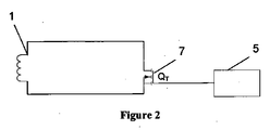
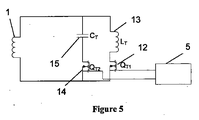
図2〜図5は主要素子のみを示す図1の簡略図である。
図2は半導体スイッチ7のみが線形モードで駆動されている抵抗性の同調手法を示す図である。この手法は、システムのフォームファクタを増加させるリアクタンス素子を必要とせずに微調整が可能になるという点で有利である。
2 to 5 are simplified views of FIG. 1 showing only main elements.
FIG. 2 is a diagram showing a resistive tuning technique in which only the
図3は半導体スイッチ8がコンデンサ9と直列である構成を含む容量性の同調手法を示すものである。この手法は、電力伝送能力の同調範囲が広い点で有利である。
図4は半導体スイッチ10がコイル11と直列である構成を含む誘導性の同調手法を示すものである。この手法は、システムに対する同調分解能を向上させることにより電力伝送能力の制御精度を向上させる点で有利である。
FIG. 3 shows a capacitive tuning technique including a configuration in which the
FIG. 4 shows an inductive tuning technique including a configuration in which the
図5は半導体スイッチ12、14が一又は複数のコイル13および一又は複数のコンデンサ15と直列である構成を含むハイブリッドの同調手法を示すものである。この手法は容量性および誘導性の長所を併せもつ。非接触受電装置の要求仕様に応じて上記装置を複数並列に用いてもよい。
FIG. 5 illustrates a hybrid tuning approach that includes a configuration in which the semiconductor switches 12, 14 are in series with one or
半導体スイッチは、非接触受電装置の出力に基いて、制御回路5によってスイッチングされる。制御回路は、コンパレータまたはオペアンプ等の単純なアナログデバイス、または参照テーブルを備えたマイクロコントローラ等の高度なデジタルデバイス、またはゲートアレイロジックデバイスを用いることよって制御を実行するようにしてもよい。
The semiconductor switch is switched by the
ピックアップコイル1の実効抵抗を変化させるために線形モードで半導体スイッチ2、3を動作させる方法は、線形モードのみで半導体スイッチ2、3を変調させる方法と、適宜、線形モードおよびスイッチモードによって変調させる方法とを含む。複数の半導体スイッチ2、3を備えた非接触受電装置においては、線形モードで動作することにより微同調をおこなうものもあれば、スイッチモードで動作することにより粗同調をおこなうものもある。要求される同調の態様に応じて、一の半導体スイッチをフル導電に切換え、他の半導体スイッチを線形モードで動作させて微同調を行ってもよい。
The method of operating the semiconductor switches 2 and 3 in the linear mode to change the effective resistance of the pickup coil 1 is a method of modulating the semiconductor switches 2 and 3 only in the linear mode, and appropriately modulating in accordance with the linear mode and the switch mode. Including a method. Some non-contact power receiving apparatuses including a plurality of
線形モードによる同調を実行する制御手法にはシュミットトリガ、比例、積分、微分制御等がある。
図6に容量性の同調を使用するシステムの構成例を示す。この実施形態ではコンデンサ23を半導体スイッチ25を用いてスイッチングすることによりピックアップコイル1の同調を行っている。この半導体スイッチはボディダイオードに加えて外部ダイオード24を備えることにより半導体スイッチ24を通じた導電損失を減少させている。コンデンサ21をピックアップコイルと並列に配置することにより非接触受電装置の同調範囲を調節している。本構成では、ハーフブリッジ整流回路をダイオード22を用いて実装している。
Control methods for performing tuning in the linear mode include Schmitt trigger, proportional, integral, and differential control.
FIG. 6 shows a configuration example of a system using capacitive tuning. In this embodiment, the pickup coil 1 is tuned by switching the
半導体スイッチ25を制御するのに用いられる制御回路装置は、端子34からのフィードバックを用いるオペアンプ28から成る。オペアンプは端子34の電圧を、ツェナーダイオード31を用いて生成する基準電圧と比較する。抵抗29、30を用いて分圧回路を実装することにより、オアンプ28への入力電圧がその最大レベル未満であり、且つ、ツェナー31により設定された基準電圧に対応することを保証している。
The control circuit device used to control the
この制御回路は、図7に示すように効果的にシュミットトリガ制御法を実行する。オペアンプには抵抗器27、26が設定されており、半導体スイッチ25を線形モードで変調するようにそのゲート駆動電圧を制御する。
This control circuit effectively executes the Schmitt trigger control method as shown in FIG.
以下に図6中の参照符号に対応する構成値を示す。 The configuration values corresponding to the reference numerals in FIG. 6 are shown below.

この非接触受電装置を平面磁界の近くに配置してもよい。これにより、ピックアップコイル1に起電力を発生させ、非接触受電装置からデバイスに給電ができるようになる。平面磁界は無線充電パッドにより形成してもよい。 You may arrange | position this non-contact power receiving apparatus near a plane magnetic field. Thereby, an electromotive force is generated in the pickup coil 1, and power can be supplied to the device from the non-contact power receiving apparatus. The planar magnetic field may be formed by a wireless charging pad.
この装置および方法は、システムの電力伝送能力がデバイスの所要電力に応じて調整されるため、非接触受電装置に電力フロー制御を実行させ、軽負荷でも効率的に動作させることができる。また、非接触受電装置は、自身を動的に同調させることができるため、システムの周波数変動を制御することができる。 In this apparatus and method, since the power transmission capability of the system is adjusted according to the required power of the device, the non-contact power receiving apparatus can execute power flow control and can be operated efficiently even with a light load. In addition, since the non-contact power receiving apparatus can dynamically tune itself, the frequency fluctuation of the system can be controlled.
このシステムは、かさばるピックアップコイルセンサを必要とせずにシステムおよび関連制御回路をソフトスイッチできるため、より少ない構成部品数、フォームファクタ、およびより簡単な回路設計でより高いQを達成することができる。 This system can soft-switch the system and associated control circuitry without the need for bulky pickup coil sensors so that higher Q can be achieved with fewer components, form factor, and simpler circuit design.
この非接触受電装置は、出力−体積比、出力−効率比、および出力−範囲比いずれの評価指標も改善できる。
本発明は実施形態の説明を通して例示した。実施形態は詳細に説明したものの、ここに付記する請求の範囲を制限、もしくはいかなる限定も加えるものではない。本発明への更なる優位点の追加および改良は当業者には容易に想到できるものである。従って,本発明を拡張した態様は、あくまでも一例として図示、説明した特定の内容や例示した装置、方法に限定されない。従って、本発明の精神、範囲から逸脱しない程度に上記実施形態を変更してもよい。
This non-contact power receiving apparatus can improve any evaluation index of output-volume ratio, output-efficiency ratio, and output-range ratio.
The invention has been illustrated throughout the description of the embodiments. Although the embodiments have been described in detail, they do not limit the scope of the claims appended hereto or add any limitation. Additions and improvements of further advantages to the present invention are readily apparent to those skilled in the art. Therefore, the aspect which extended this invention is not limited to the specific content illustrated and demonstrated as an example to the last, and the illustrated apparatus and method. Therefore, the above-described embodiment may be changed without departing from the spirit and scope of the present invention.
本発明は、誘導結合電力伝送システム(ICPT)の技術分野に関するものである。具体的には本発明は線形モードで動作する半導体素子を備えた非接触受電装置に関する。 The present invention relates to the technical field of inductively coupled power transfer systems (ICPT). Specifically, the present invention relates to a contactless power receiving device including a semiconductor element that operates in a linear mode.
非接触電力システムは、電源から交流電流の供給を受ける導電経路を有する非接触送電装置と、一又は複数の非接触受電装置とを備えている。これらの非接触受電装置は導電経路の近傍に配置されるが、電気的には導電経路から絶縁されている。非接触受電装置は導電経路により形成される磁界によって電圧が誘起されるピックアップコイルを備え、電気負荷を提供するものである。通常、ピックアップコイルは、システムの電力伝送能力を高めるために同調コンデンサを用いて同調がなされる。 The non-contact power system includes a non-contact power transmission device having a conductive path that receives supply of alternating current from a power source, and one or a plurality of non-contact power reception devices. These non-contact power receiving devices are disposed in the vicinity of the conductive path, but are electrically insulated from the conductive path. The non-contact power receiving apparatus includes a pickup coil whose voltage is induced by a magnetic field formed by a conductive path, and provides an electric load. Typically, the pickup coil is tuned with a tuning capacitor to increase the power transfer capability of the system.
非接触受電装置における問題点の一つは、軽負荷時例えば受電装置から給電を受けるモータが制御システムからの指令待機中であり、停止している時に、効率が低下することである。これはピックアップコイルと負荷の間で、電力制御装置を介して電力の流れを制御することで解決可能である。 One of the problems in the non-contact power receiving device is that the efficiency decreases when the motor receiving power from the power receiving device is waiting for a command from the control system at a light load and is stopped. This can be solved by controlling the flow of power between the pickup coil and the load via a power control device.
電力制御装置として、ピックアップ回路の一部に短絡スイッチを用いること事により、適宜、ピックアップコイルを負荷から切り離すものがある。このような手法は、Auckland UniServices Limitedへ譲渡された米国特許5、293、308の明細書に「短絡制御」として記載されている。 Some power control devices use a short-circuit switch in a part of the pickup circuit to appropriately disconnect the pickup coil from the load. Such a technique is described as “short circuit control” in US Pat. No. 5,293,308 assigned to Auckland UniServices Limited.
上記に記載された技術は、ピックアップ側から負荷側への電力の流れ制御の問題については解決するものの、特に軽負荷時においては、ピックアップ回路がほぼ常に、無負荷または軽負荷の状態で短絡されるため、短絡スイッチにより大きな導電損失が発生する可能性がある。 Although the technique described above solves the problem of power flow control from the pickup side to the load side, the pickup circuit is almost always short-circuited in a no-load or light-load state, especially at light loads. Therefore, a large conductive loss may occur due to the short-circuit switch.
また、非接触電力システムにおける別の問題点として、負荷状態およびその他の回路パラメータの変化に起因する周波数変動がある。これによりピックアップコイルにおける誘起電圧の大きさおよび短絡回路の電流が変化し、システムの電力伝送能力に影響する可能性がある。これは固定的または受動的に同調がなされる非接触受電装置において特に問題となる。 Another problem in the non-contact power system is frequency fluctuations caused by changes in load conditions and other circuit parameters. As a result, the magnitude of the induced voltage in the pickup coil and the current in the short circuit change, which may affect the power transmission capability of the system. This is particularly a problem in contactless power receiving devices that are tuned either fixedly or passively.
米国特許明細書US2007/109708A1およびUS7、382、636B2に記載の手法では、受電装置の実効キャパシタンスまたは実効インダクタンスを変化させることによって電力ピックアップを動的に同調させまたは非同調としている。これにより非接触受電装置において、パラメータの変化に起因する周波数ドリフトの補償が可能になる。実効キャパシタンスまたは実効インダクタンスの変更は、コンデンサまたはコイルに直列接続された2つの半導体スイッチを用いて行う。更には可変コンデンサまたは可変抵抗のソフトスイッチングを実現するためにピックアップコイル電流の大きさおよび位相の検知手段が必要である。動的な同調を行うことにより、周波数ドリフトの補償のみならず、ピックアップコイルの共振周波数の微調整が可能になるため、受動的な同調システム(通常Q<6)と比較して、品質係数(Q>10)を大幅に増加させることができる。品質係数が高いとシステムの電力伝送能力を向上させる。 In the approach described in US patent specifications US2007 / 109708A1 and US7,382,636B2, the power pickup is dynamically tuned or untuned by changing the effective capacitance or effective inductance of the power receiving device. Thereby, in the non-contact power receiving apparatus, it is possible to compensate for the frequency drift caused by the parameter change. The effective capacitance or effective inductance is changed by using two semiconductor switches connected in series with a capacitor or a coil. Furthermore, a means for detecting the magnitude and phase of the pickup coil current is required to realize soft switching of the variable capacitor or variable resistor. Dynamic tuning allows not only compensation for frequency drift, but also fine tuning of the resonance frequency of the pickup coil, so compared to passive tuning systems (usually Q <6), the quality factor ( Q> 10) can be greatly increased. A high quality factor improves the power transfer capability of the system.
非接触電力ピックアップ回路の小型化を図る上では、高い周波数で特に複雑化するピックアップコイルセンサを省くとよい。ただし、これを省くことにより可変コンデンサまたは可変コイルをソフトスイッチすることができなくなる、即ち、システムがハードスイッチされるようになる。この手法は、スイッチング途中においてコイル電流が遮断され或いはコンデンサが短絡されるので、過大な電流または電圧を発生させる。その結果生じるスイッチング過度現象は、EMI、同調を行う半導体スイッチのストレスを引き起こすと共に過度の電力損失によりシステムの電力効率を低下させる。そして最悪の場合、システム障害が起きることもある。 In order to reduce the size of the non-contact power pickup circuit, it is preferable to omit a pickup coil sensor that is particularly complicated at a high frequency. However, if this is omitted, the variable capacitor or the variable coil cannot be soft-switched, that is, the system is hard-switched. This method generates excessive current or voltage because the coil current is cut off or the capacitor is short-circuited during switching. The resulting switching transients cause stress in the semiconductor switch that performs the EMI and tuning and reduce the power efficiency of the system due to excessive power loss. In the worst case, a system failure may occur.
本発明の目的は、既存のシステムの抱える一又は複数の問題点を改善する非接触受電装置の制御方法、または装置を提供する、若しくは少なくとも公共に有益な代替手段を提供することにある。 It is an object of the present invention to provide a control method or apparatus for a non-contact power receiving apparatus that improves one or more problems of existing systems, or at least to provide a publicly useful alternative.
本発明の一実施形態において提供する、以下を備える近接場誘導結合電力伝送システムにおける使用に適した非接触受電装置。
a.ピックアップコイル、
b.ピックアップコイルを通して流れる電流を制御する一又は複数の半導体素子、および
c.前記非接触受電装置の出力に基づいて前記受電装置の同調を行うために、少なくとも一つの半導体素子を、少なくともその動作範囲の一部に亘って線形モードで駆動する制御回路。
A non-contact power receiving apparatus suitable for use in a near-field inductively coupled power transmission system provided in an embodiment of the present invention, comprising:
a. Pickup coil,
b. One or more semiconductor elements that control the current flowing through the pickup coil ; and c. A control circuit that drives at least one semiconductor element in a linear mode over at least a portion of its operating range to tune the power receiving device based on the output of the non-contact power receiving device.
更なる実施形態において提供する、電子デバイスと共に使用するシステムは以下を備える。
a.磁界を形成するコイルに通電させる駆動回路を有する送電装置
b.上記記載の受電装置であって、電子デバイスに、エネルギー蓄積デバイスを介して、または直接接続された前記受電装置。
A system for use with an electronic device provided in a further embodiment comprises:
a. A power transmission device having a drive circuit for energizing a coil forming a magnetic field; b. The power receiving apparatus as described above, wherein the power receiving apparatus is connected to an electronic device via an energy storage device or directly .
更なる実施形態において提供する、送電装置によって磁界を介して受電装置のピックアップコイルに電力を送る非接触電力システムにおいて用いる方法であって、前記受電装置の少なくとも一部の動作範囲に亘って、前記受電装置のピックアップコイルに付与される抵抗を変化させることによって前記受電装置を同調する方法。 Provided in a further embodiment is a method for use in a non-contact power system for transmitting power to a pickup coil of a power receiving device via a magnetic field by a power transmitting device, the operation being performed over at least a part of the operating range of the power receiving device. A method of tuning the power receiving device by changing a resistance applied to a pickup coil of the power receiving device.
更なる実施形態において提供する、以下を備える近接場誘導結合電力送信システムにおける使用に適した非接触受電装置。
a.ピックアップコイルの入力部、
b.前記ピックアップコイルの入力部に接続された一又は複数の半導体素子、および
c.前記ピックアップコイルの前記入力部に接続されて使用される制御回路であって、
前記非接触受電装置の出力に基づいて前記受電装置の同調を行うために、少なくとも一つの半導体素子を、少なくともその動作範囲の一部に亘って線形モードで駆動する制御回路。
A contactless power receiving device suitable for use in a near-field inductively coupled power transmission system provided in a further embodiment comprising:
a. Pickup coil input section,
b. One or more semiconductor elements connected to the input of the pickup coil ; and c. A control circuit used by being connected to the input section of the pickup coil;
A control circuit that drives at least one semiconductor element in a linear mode over at least a portion of its operating range to tune the power receiving device based on the output of the non-contact power receiving device.
付属の図面は明細書の一部を構成し、本発明の実施形態を図示するものであり、上記の発明の概要の説明および下記の実施形態の詳細な説明と共に発明の原理を説明する。
図1に一又は複数の半導体素子2、3に接続されたピックアップコイル1を備えた非接触受電装置を示す。これらの半導体素子2、3は、これら半導体素子2、3を変調する制御回路5によって駆動される。図示の構成ではフルまたはハーフブリッジ整流回路4を備えることにより、直流を制御回路5および電子デバイスまたはエネルギー蓄積デバイス6へ供給している。
FIG. 1 shows a non-contact power receiving apparatus including a pickup coil 1 connected to one or a plurality of
磁界に近づくとピックアップコイル1に起電力が発生する。従来のトランスと比較して磁界とピックアップコイル1の磁気結合は非常に弱いため、通常、誘起電圧はそのまま使用するのには適さない。 When the magnetic field is approached, an electromotive force is generated in the pickup coil 1. Since the magnetic coupling between the magnetic field and the pickup coil 1 is very weak compared to a conventional transformer, the induced voltage is usually not suitable for use as it is.
電子デバイスまたはエネルギー蓄積デバイス6の所要電力に応じて電力を制御する電力制御装置が必要になる。また、システムの電力伝送能力を高めるためにはピックアップコイル1を同調させる必要がある。その際、動的な同調方法を用いて電力の制御、ピックアップコイル1の同調、ひいてはシステムの電力伝送能力を増減させてもよい。この補償法を用いることにより、更に非接触受電装置によるシステム周波数の変動に追従できるようになる。 A power control device that controls the power according to the required power of the electronic device or the energy storage device 6 is required. Further, in order to increase the power transmission capability of the system, it is necessary to tune the pickup coil 1. At that time, dynamic control may be used to control power, tune the pickup coil 1, and thus increase or decrease the power transmission capacity of the system. By using this compensation method, it becomes possible to follow the fluctuation of the system frequency by the non-contact power receiving apparatus.
発明者らはオーミックな線形モードで動作する半導体素子2、3を変調する非接触受電装置を動的に同調させる方が、スイッチモードによる切換えよりも性能が優位であることを見出した。
The inventors have found that the performance of tuning the contactless power receiving device that modulates the
アクティブスイッチモードに基づいて同調させる場合、システムをソフトスイッチにより切り替えなければならず、そのためにはピックアップコイル1の位相と大きさを検知する電流センサが必要になる。センサは概して大型なデバイスであり、専用の信号処理回路を必要とすることが多い。 When tuning based on the active switch mode, the system must be switched by a soft switch, which requires a current sensor that detects the phase and size of the pickup coil 1. Sensors are generally large devices and often require dedicated signal processing circuitry.
センサを用いずにアクティブスイッチモードに基づいた同調を行う場合、デバイスをいわゆるハードスイッチするということになり、対応する半導体素子のON時に容量性または誘導性の同調素子が実効的に短絡される。これによりEMIの原因となり、容量性または誘導性の同調素子および半導体素子自身にストレスを与えるスイッチング過度現象を引き起こし、システム全体の効率と信頼性を悪化させる。 When performing tuning based on active switch mode without using a sensor, will be referred to so-called hard switch device, the corresponding semiconductor elements turned ON, the capacitive or inductive tuning element is effectively shorted. This causes EMI and causes switching transients that stress the capacitive or inductive tuning element and the semiconductor element itself, degrading the efficiency and reliability of the overall system.
半導体素子はON時にオーミック(線形)またはアクティブ(飽和/フル導電)領域で動作する。半導体素子がOFFとON−オーミック領域の間を繰り返す場合、線形モードで動作しているとされる。OFFとON−アクティブ領域の間を繰り返す場合、スイッチモードで動作しているとされる。 The semiconductor device operates in an ohmic (linear) or active (saturated / full conductive) region when ON. When the semiconductor element repeats between the OFF and ON-ohmic regions, it is said that it is operating in a linear mode. When repeating between the OFF and ON-active regions, it is assumed that the switch is operating in the switch mode.
半導体素子を線形モードで動作させることで素子が容量性または誘導性の同調素子と共に抵抗素子として機能するため、これらの問題を解決することができる。例えばMOSFETの半導体素子の場合、ゲート駆動電圧をMOSFETのオーミック領域内で制御することによりこれを実現する。 Since the element by operating the semiconductor device in a linear mode to function as a resistance element with a capacitive or inductive tuning element, it is possible to solve these problems. For example, in the case of a MOSFET semiconductor device , this is realized by controlling the gate drive voltage within the ohmic region of the MOSFET.
図2〜図5は主要素子のみを示す図1の簡略図である。
図2は半導体素子7のみが線形モードで駆動されている抵抗性の同調手法を示す図である。この手法は、システムのフォームファクタを増加させるリアクタンス素子を必要とせずに微調整が可能になるという点で有利である。
2 to 5 are simplified views of FIG. 1 showing only main elements.
FIG. 2 is a diagram showing a resistive tuning technique in which only the
図3は半導体素子8がコンデンサ9と直列である構成を含む容量性の同調手法を示すものである。この手法は、電力伝送能力の同調範囲が広い点で有利である。
図4は半導体素子10がコイル11と直列である構成を含む誘導性の同調手法を示すものである。この手法は、システムに対する同調分解能を向上させることにより電力伝送能力の制御精度を向上させる点で有利である。
FIG. 3 shows a capacitive tuning technique including a configuration in which the
FIG. 4 shows an inductive tuning technique including a configuration in which the
図5は半導体素子12、14が一又は複数のコイル13および一又は複数のコンデンサ15と直列である構成を含むハイブリッドの同調手法を示すものである。この手法は容量性および誘導性の長所を併せもつ。非接触受電装置の要求仕様に応じて上記装置を複数並列に用いてもよい。
FIG. 5 illustrates a hybrid tuning technique that includes a configuration in which the
半導体素子は、非接触受電装置の出力に基いて、制御回路5によってスイッチングされる。制御回路は、コンパレータまたはオペアンプ等の単純なアナログデバイス、または参照テーブルを備えたマイクロコントローラ等の高度なデジタルデバイス、またはゲートアレイロジックデバイスを用いることよって制御を実行するようにしてもよい。
The semiconductor element is switched by the
ピックアップコイル1の実効抵抗を変化させるために線形モードで半導体素子2、3を動作させる方法は、線形モードのみで半導体素子2、3を変調させる方法と、適宜、線形モードおよびスイッチモードによって変調させる方法とを含む。複数の半導体素子2、3を備えた非接触受電装置においては、線形モードで動作することにより微同調をおこなうものもあれば、スイッチモードで動作することにより粗同調をおこなうものもある。要求される同調の態様に応じて、一の半導体素子をフル導電に切換え、他の半導体素子を線形モードで動作させて微同調を行ってもよい。
The method of operating the
線形モードによる同調を実行する制御手法にはシュミットトリガ、比例、積分、微分制御等がある。
図6に容量性の同調を使用するシステムの構成例を示す。この実施形態ではコンデンサ23を半導体素子25を用いてスイッチングすることによりピックアップコイル1の同調を行っている。この半導体素子はボディダイオードに加えて外部ダイオード24を備えることにより半導体素子24を通じた導電損失を減少させている。コンデンサ21をピックアップコイルと並列に配置することにより非接触受電装置の同調範囲を調節している。本構成では、ハーフブリッジ整流回路をダイオード22を用いて実装している。
Control methods for performing tuning in the linear mode include Schmitt trigger, proportional, integral, and differential control.
FIG. 6 shows a configuration example of a system using capacitive tuning. In this embodiment, the pickup coil 1 is tuned by switching the
半導体素子25を制御するのに用いられる制御回路装置は、端子34からのフィードバックを用いるオペアンプ28から成る。オペアンプは端子34の電圧を、ツェナーダイオード31を用いて生成する基準電圧と比較する。抵抗29、30を用いて分圧回路を実装することにより、オアンプ28への入力電圧がその最大レベル未満であり、且つ、ツェナー31により設定された基準電圧に対応することを保証している。
The control circuit device used to control the
この制御回路は、図7に示すように効果的にシュミットトリガ制御法を実行する。オペアンプには抵抗器27、26が設定されており、半導体素子25を線形モードで変調するようにそのゲート駆動電圧を制御する。
This control circuit effectively executes the Schmitt trigger control method as shown in FIG.
以下に図6中の参照符号に対応する構成値を示す。 The configuration values corresponding to the reference numerals in FIG. 6 are shown below.
この非接触受電装置を平面磁界の近くに配置してもよい。これにより、ピックアップコイル1に起電力を発生させ、非接触受電装置からデバイスに給電ができるようになる。平面磁界は無線充電パッドにより形成してもよい。 You may arrange | position this non-contact power receiving apparatus near a plane magnetic field. Thereby, an electromotive force is generated in the pickup coil 1, and power can be supplied to the device from the non-contact power receiving apparatus. The planar magnetic field may be formed by a wireless charging pad.
この装置および方法は、システムの電力伝送能力がデバイスの所要電力に応じて調整されるため、非接触受電装置に電力フロー制御を実行させ、軽負荷でも効率的に動作させることができる。また、非接触受電装置は、自身を動的に同調させることができるため、システムの周波数変動を制御することができる。 In this apparatus and method, since the power transmission capability of the system is adjusted according to the required power of the device, the non-contact power receiving apparatus can execute power flow control and can be operated efficiently even with a light load. In addition, since the non-contact power receiving apparatus can dynamically tune itself, the frequency fluctuation of the system can be controlled.
このシステムは、かさばるピックアップコイルセンサを必要とせずにシステムおよび関連制御回路をソフトスイッチできるため、より少ない構成部品数、フォームファクタ、およびより簡単な回路設計でより高いQを達成することができる。 This system can soft-switch the system and associated control circuitry without the need for bulky pickup coil sensors so that higher Q can be achieved with fewer components, form factor, and simpler circuit design.
この非接触受電装置は、出力−体積比、出力−効率比、および出力−範囲比いずれの評価指標も改善できる。
本発明は実施形態の説明を通して例示した。実施形態は詳細に説明したものの、ここに付記する請求の範囲を制限、もしくはいかなる限定も加えるものではない。本発明への更なる優位点の追加および改良は当業者には容易に想到できるものである。従って,本発明を拡張した態様は、あくまでも一例として図示、説明した特定の内容や例示した装置、方法に限定されない。従って、本発明の精神、範囲から逸脱しない程度に上記実施形態を変更してもよい。
This non-contact power receiving apparatus can improve any evaluation index of output-volume ratio, output-efficiency ratio, and output-range ratio.
The invention has been illustrated throughout the description of the embodiments. Although the embodiments have been described in detail, they do not limit the scope of the claims appended hereto or add any limitation. Additions and improvements of further advantages to the present invention are readily apparent to those skilled in the art. Therefore, the aspect which extended this invention is not limited to the specific content illustrated and demonstrated as an example to the last, and the illustrated apparatus and method. Therefore, the above-described embodiment may be changed without departing from the spirit and scope of the present invention.
Claims (20)
a.ピックアップコイル、
b.ピックアップコイルと回路を形成する一又は複数の半導体スイッチ、および
c.前記非接触受電装置の出力に基づいて前記受電装置の同調を行うために、一又は複数の半導体スイッチを、少なくともその動作範囲の一部に亘って線形モードで駆動する制御回路。 A non-contact power receiving device comprising:
a. Pickup coil,
b. One or more semiconductor switches forming a circuit with the pickup coil; and c. A control circuit that drives one or more semiconductor switches in a linear mode over at least part of their operating range to tune the power receiving device based on the output of the non-contact power receiving device.
a.磁界を形成するコイルに通電させる駆動回路を有する送電装置、
b.請求項1から10のいずれか1つに記載の受電装置であって、 電子デバイスに、エネルギー蓄積デバイスを介してまたは直接接続された受電装置。 A system for use with an electronic device comprising:
a. A power transmission device having a drive circuit for energizing a coil that forms a magnetic field;
b. The power receiving device according to any one of claims 1 to 10, wherein the power receiving device is connected to an electronic device via an energy storage device or directly.
a.ピックアップコイルの入力部、
b.前記ピックアップコイルの入力部に接続された一又は複数の半導体スイッチ、および
c.前記ピックアップコイルの前記入力部に接続されたピックアップコイルとともに使用されるときに、前記非接触受電装置の出力に基づいて前記受電装置の同調を行うために、一又は複数の半導体スイッチを、少なくともその動作範囲の一部に亘って線形モードで駆動する制御回路。 A non-contact power receiving device comprising:
a. Pickup coil input section,
b. One or more semiconductor switches connected to the input of the pickup coil; and c. In order to tune the power receiving device based on the output of the non-contact power receiving device when used with a pickup coil connected to the input portion of the pickup coil, at least one semiconductor switch is provided. A control circuit that drives in a linear mode over part of the operating range.
Applications Claiming Priority (3)
| Application Number | Priority Date | Filing Date | Title |
|---|---|---|---|
| NZ569615 | 2008-07-07 | ||
| NZ56961508 | 2008-07-07 | ||
| PCT/NZ2009/000137 WO2010005324A1 (en) | 2008-07-07 | 2009-07-07 | A contactless power receiver and method of operation |
Related Child Applications (1)
| Application Number | Title | Priority Date | Filing Date |
|---|---|---|---|
| JP2014009417A Division JP5816308B2 (en) | 2008-07-07 | 2014-01-22 | Non-contact power receiving apparatus and operation method thereof |
Publications (1)
| Publication Number | Publication Date |
|---|---|
| JP2011527558A true JP2011527558A (en) | 2011-10-27 |
Family
ID=41507264
Family Applications (2)
| Application Number | Title | Priority Date | Filing Date |
|---|---|---|---|
| JP2011517373A Pending JP2011527558A (en) | 2008-07-07 | 2009-07-07 | Non-contact power receiving apparatus and operation method thereof |
| JP2014009417A Active JP5816308B2 (en) | 2008-07-07 | 2014-01-22 | Non-contact power receiving apparatus and operation method thereof |
Family Applications After (1)
| Application Number | Title | Priority Date | Filing Date |
|---|---|---|---|
| JP2014009417A Active JP5816308B2 (en) | 2008-07-07 | 2014-01-22 | Non-contact power receiving apparatus and operation method thereof |
Country Status (6)
| Country | Link |
|---|---|
| US (1) | US9124113B2 (en) |
| EP (1) | EP2311052B1 (en) |
| JP (2) | JP2011527558A (en) |
| CN (3) | CN104022580A (en) |
| NZ (1) | NZ590978A (en) |
| WO (1) | WO2010005324A1 (en) |
Families Citing this family (62)
| Publication number | Priority date | Publication date | Assignee | Title |
|---|---|---|---|---|
| US7065658B1 (en) | 2001-05-18 | 2006-06-20 | Palm, Incorporated | Method and apparatus for synchronizing and recharging a connector-less portable computer system |
| US7952322B2 (en) | 2006-01-31 | 2011-05-31 | Mojo Mobility, Inc. | Inductive power source and charging system |
| US11201500B2 (en) | 2006-01-31 | 2021-12-14 | Mojo Mobility, Inc. | Efficiencies and flexibilities in inductive (wireless) charging |
| US8169185B2 (en) | 2006-01-31 | 2012-05-01 | Mojo Mobility, Inc. | System and method for inductive charging of portable devices |
| US7948208B2 (en) | 2006-06-01 | 2011-05-24 | Mojo Mobility, Inc. | Power source, charging system, and inductive receiver for mobile devices |
| US11329511B2 (en) | 2006-06-01 | 2022-05-10 | Mojo Mobility Inc. | Power source, charging system, and inductive receiver for mobile devices |
| US20110050164A1 (en) | 2008-05-07 | 2011-03-03 | Afshin Partovi | System and methods for inductive charging, and improvements and uses thereof |
| NZ590978A (en) | 2008-07-07 | 2014-01-31 | Powerbyproxi Ltd | A contactless power receiver and method of operation |
| USD640976S1 (en) | 2008-08-28 | 2011-07-05 | Hewlett-Packard Development Company, L.P. | Support structure and/or cradle for a mobile computing device |
| EP2329585B1 (en) * | 2008-09-11 | 2021-04-21 | Auckland UniServices Limited | Inductively coupled ac power transfer |
| US8850045B2 (en) | 2008-09-26 | 2014-09-30 | Qualcomm Incorporated | System and method for linking and sharing resources amongst devices |
| US8868939B2 (en) | 2008-09-26 | 2014-10-21 | Qualcomm Incorporated | Portable power supply device with outlet connector |
| US8712324B2 (en) | 2008-09-26 | 2014-04-29 | Qualcomm Incorporated | Inductive signal transfer system for computing devices |
| US8401469B2 (en) | 2008-09-26 | 2013-03-19 | Hewlett-Packard Development Company, L.P. | Shield for use with a computing device that receives an inductive signal transmission |
| US8688037B2 (en) | 2008-09-26 | 2014-04-01 | Hewlett-Packard Development Company, L.P. | Magnetic latching mechanism for use in mating a mobile computing device to an accessory device |
| US8234509B2 (en) | 2008-09-26 | 2012-07-31 | Hewlett-Packard Development Company, L.P. | Portable power supply device for mobile computing devices |
| US8385822B2 (en) | 2008-09-26 | 2013-02-26 | Hewlett-Packard Development Company, L.P. | Orientation and presence detection for use in configuring operations of computing devices in docked environments |
| US8527688B2 (en) | 2008-09-26 | 2013-09-03 | Palm, Inc. | Extending device functionality amongst inductively linked devices |
| US9083686B2 (en) | 2008-11-12 | 2015-07-14 | Qualcomm Incorporated | Protocol for program during startup sequence |
| EP2377296B1 (en) | 2009-01-05 | 2019-10-16 | QUALCOMM Incorporated | Interior connector scheme for accessorizing a mobile computing device with a removeable housing segment |
| US8954001B2 (en) | 2009-07-21 | 2015-02-10 | Qualcomm Incorporated | Power bridge circuit for bi-directional wireless power transmission |
| US8437695B2 (en) | 2009-07-21 | 2013-05-07 | Hewlett-Packard Development Company, L.P. | Power bridge circuit for bi-directional inductive signaling |
| US9395827B2 (en) | 2009-07-21 | 2016-07-19 | Qualcomm Incorporated | System for detecting orientation of magnetically coupled devices |
| US8755815B2 (en) | 2010-08-31 | 2014-06-17 | Qualcomm Incorporated | Use of wireless access point ID for position determination |
| US8395547B2 (en) | 2009-08-27 | 2013-03-12 | Hewlett-Packard Development Company, L.P. | Location tracking for mobile computing device |
| USD674391S1 (en) | 2009-11-17 | 2013-01-15 | Hewlett-Packard Development Company, L.P. | Docking station for a computing device |
| EP2580844A4 (en) | 2010-06-11 | 2016-05-25 | Mojo Mobility Inc | System for wireless power transfer that supports interoperability, and multi-pole magnets for use therewith |
| CN103222319B (en) | 2010-09-29 | 2016-08-10 | 高通股份有限公司 | A kind of method for mobile computing device and mobile computing device |
| CA2815035A1 (en) * | 2010-10-20 | 2012-04-26 | Chiesi Farmaceutici S.P.A. | Carbonate derivatives for the treatment of cough |
| NZ607488A (en) | 2010-11-16 | 2014-08-29 | Powerbyproxi Ltd | A wirelessly rechargeable battery and power transmitter |
| US9496732B2 (en) | 2011-01-18 | 2016-11-15 | Mojo Mobility, Inc. | Systems and methods for wireless power transfer |
| US9178369B2 (en) | 2011-01-18 | 2015-11-03 | Mojo Mobility, Inc. | Systems and methods for providing positioning freedom, and support of different voltages, protocols, and power levels in a wireless power system |
| US10115520B2 (en) | 2011-01-18 | 2018-10-30 | Mojo Mobility, Inc. | Systems and method for wireless power transfer |
| US9356659B2 (en) | 2011-01-18 | 2016-05-31 | Mojo Mobility, Inc. | Chargers and methods for wireless power transfer |
| US11342777B2 (en) | 2011-01-18 | 2022-05-24 | Mojo Mobility, Inc. | Powering and/or charging with more than one protocol |
| NZ593946A (en) * | 2011-07-07 | 2014-05-30 | Powerbyproxi Ltd | An inductively coupled power transfer receiver |
| CN102361357B (en) * | 2011-09-22 | 2013-06-26 | 重庆大学 | CPT (contact-less power transfer) system based on static capacitor array and control method thereof |
| JP5748628B2 (en) * | 2011-09-28 | 2015-07-15 | 株式会社アドバンテスト | Wireless power receiving device and wireless power feeding device |
| JP5702696B2 (en) * | 2011-09-28 | 2015-04-15 | 株式会社アドバンテスト | Wireless power receiving device, wireless power feeding device, and wireless power feeding system |
| KR102042498B1 (en) * | 2012-01-11 | 2019-11-11 | 삼성전자주식회사 | Overvoltage protecting device for resonance wireless power receiving apparatus and controlling method thereof |
| US9722447B2 (en) | 2012-03-21 | 2017-08-01 | Mojo Mobility, Inc. | System and method for charging or powering devices, such as robots, electric vehicles, or other mobile devices or equipment |
| KR102139841B1 (en) | 2012-10-29 | 2020-07-31 | 애플 인크. | A receiver for an inductive power transfer system and a method for controlling the receiver |
| US9368975B2 (en) | 2012-11-30 | 2016-06-14 | Qualcomm Incorporated | High power RF field effect transistor switching using DC biases |
| US9837846B2 (en) | 2013-04-12 | 2017-12-05 | Mojo Mobility, Inc. | System and method for powering or charging receivers or devices having small surface areas or volumes |
| US10164472B2 (en) | 2013-12-03 | 2018-12-25 | Massachusetts Institute Of Technology | Method and apparatus for wirelessly charging portable electronic devices |
| JP6830890B2 (en) | 2014-11-05 | 2021-02-17 | アップル インコーポレイテッドApple Inc. | Inductive power receiver |
| US10498160B2 (en) | 2015-08-03 | 2019-12-03 | Massachusetts Institute Of Technology | Efficiency maximization for device-to-device wireless charging |
| CN108432087B (en) | 2015-11-05 | 2021-06-15 | 蒂克森能量责任有限公司 | Method and device for obtaining power intended to supply an electrical consumer from a conductor traversed by an alternating current |
| SG10201700633QA (en) | 2016-02-03 | 2017-09-28 | Gen Electric | System and method for protecting a wireless power transfer system |
| JP7049768B2 (en) | 2016-02-03 | 2022-04-07 | ゼネラル・エレクトリック・カンパニイ | Methods and systems for protecting wireless power transfer systems |
| KR101846954B1 (en) * | 2016-06-13 | 2018-04-10 | 주식회사 맵스 | Wireless power transmitting unit capable auto-tunning in response to impedance variance of load |
| EP3280030B1 (en) | 2016-08-04 | 2023-08-30 | General Electric Company | System and method for charging receiver devices |
| US10224873B1 (en) | 2016-09-22 | 2019-03-05 | Apple Inc. | Voltage collection bootstrap circuit |
| SG10201707385XA (en) * | 2016-09-30 | 2018-04-27 | Gen Electric | Over voltage protection for a wireless power transfer system |
| SG10201708314TA (en) | 2016-10-28 | 2018-05-30 | Gen Electric | System and method for actively controlling output voltage of a wireless power transfer system |
| US10355532B2 (en) | 2016-11-02 | 2019-07-16 | Apple Inc. | Inductive power transfer |
| US10447090B1 (en) | 2016-11-17 | 2019-10-15 | Apple Inc. | Inductive power receiver |
| US10283952B2 (en) | 2017-06-22 | 2019-05-07 | Bretford Manufacturing, Inc. | Rapidly deployable floor power system |
| US10651687B2 (en) | 2018-02-08 | 2020-05-12 | Massachusetts Institute Of Technology | Detuning for a resonant wireless power transfer system including cryptography |
| US11018526B2 (en) | 2018-02-08 | 2021-05-25 | Massachusetts Institute Of Technology | Detuning for a resonant wireless power transfer system including cooperative power sharing |
| US11444485B2 (en) | 2019-02-05 | 2022-09-13 | Mojo Mobility, Inc. | Inductive charging system with charging electronics physically separated from charging coil |
| CN111342565A (en) * | 2020-03-19 | 2020-06-26 | 许继集团有限公司 | Electric power wireless transmission coupling device and system |
Citations (9)
| Publication number | Priority date | Publication date | Assignee | Title |
|---|---|---|---|---|
| JPH10145987A (en) * | 1996-09-13 | 1998-05-29 | Hitachi Ltd | Power transmission system, ic card and information communicating system using ic card |
| JPH10187916A (en) * | 1996-12-27 | 1998-07-21 | Rohm Co Ltd | Responder for contactless ic card communication system |
| JP2000242756A (en) * | 1999-02-25 | 2000-09-08 | Well Cat:Kk | Data carrier having charging function |
| JP2001005938A (en) * | 1999-04-19 | 2001-01-12 | Denso Corp | Non-contact ic card |
| JP2002078247A (en) * | 2000-08-23 | 2002-03-15 | Nippon Telegr & Teleph Corp <Ntt> | Electromagnetic field receiving apparatus |
| JP2003111312A (en) * | 2001-10-01 | 2003-04-11 | Sharp Corp | Radio wave power supply system |
| JP2004072832A (en) * | 2002-08-02 | 2004-03-04 | Hitachi Kiden Kogyo Ltd | Non-contact power feeding method |
| JP2005525705A (en) * | 2002-05-13 | 2005-08-25 | スプラッシュパワー リミテッド | Improvements for contactless power transmission |
| WO2007138690A1 (en) * | 2006-05-31 | 2007-12-06 | Hitachi, Ltd. | Noncontact type electronic device and semiconductor integrated circuit device mounted on same |
Family Cites Families (41)
| Publication number | Priority date | Publication date | Assignee | Title |
|---|---|---|---|---|
| US4654573A (en) * | 1985-05-17 | 1987-03-31 | Flexible Manufacturing Systems, Inc. | Power transfer device |
| NL8701565A (en) * | 1987-07-03 | 1989-02-01 | Nedap Nv | IDENTIFICATION SYSTEM WITH TWO OPERATING MODES. |
| EP0398943B1 (en) | 1988-02-04 | 1995-12-06 | Magellan Corporation (Australia) Pty. Ltd. | Shunt regulator |
| US5311198A (en) * | 1990-08-23 | 1994-05-10 | The United States Of America As Represented By The Administrator Of The National Aeronautics And Space Administration | Active antenna |
| US5293308A (en) * | 1991-03-26 | 1994-03-08 | Auckland Uniservices Limited | Inductive power distribution system |
| US5450305A (en) * | 1991-08-12 | 1995-09-12 | Auckland Uniservices Limited | Resonant power supplies |
| NZ274939A (en) | 1993-10-21 | 1997-06-24 | Auckland Uniservices Ltd | Inductive power pick-up coils best aligned activated by controller |
| US5596567A (en) | 1995-03-31 | 1997-01-21 | Motorola, Inc. | Wireless battery charging system |
| SG54559A1 (en) * | 1996-09-13 | 1998-11-16 | Hitachi Ltd | Power transmission system ic card and information communication system using ic card |
| DE19836401A1 (en) * | 1997-09-19 | 2000-02-17 | Salcomp Oy Salo | Device for charging accumulators |
| FR2792130B1 (en) * | 1999-04-07 | 2001-11-16 | St Microelectronics Sa | ELECTROMAGNETIC TRANSPONDER WITH VERY CLOSE COUPLING OPERATION |
| US7522878B2 (en) * | 1999-06-21 | 2009-04-21 | Access Business Group International Llc | Adaptive inductive power supply with communication |
| US6445936B1 (en) * | 1999-11-16 | 2002-09-03 | Agere Systems Guardian Corp. | Low power consumption quick charge for wireless device |
| JP2001218280A (en) * | 2000-02-02 | 2001-08-10 | Sony Corp | Power supply unit for electronic equipment |
| US6229443B1 (en) * | 2000-06-23 | 2001-05-08 | Single Chip Systems | Apparatus and method for detuning of RFID tag to regulate voltage |
| JP4135299B2 (en) | 2000-06-27 | 2008-08-20 | 松下電工株式会社 | Non-contact power transmission device |
| FR2811108B1 (en) * | 2000-06-29 | 2002-09-27 | A S K | NON-CONTACT PERIPHERAL DISPLAY DEVICE FOR NON-CONTACT PORTABLE OBJECT |
| FI20002493A (en) * | 2000-11-14 | 2002-05-15 | Salcomp Oy | Power Supply Arrangement and Inductively Connected Battery Charger with Wireless Connected Control, and Method for Wirelessly Controlling Power Supply Arrangement and Inductively Connected Battery Charger |
| JP2003309982A (en) | 2002-04-16 | 2003-10-31 | Mitsubishi Electric Corp | Power semiconductor device |
| GB0210886D0 (en) | 2002-05-13 | 2002-06-19 | Zap Wireless Technologies Ltd | Improvements relating to contact-less power transfer |
| US7239110B2 (en) * | 2002-05-13 | 2007-07-03 | Splashpower Limited | Primary units, methods and systems for contact-less power transfer |
| NZ526115A (en) | 2003-05-23 | 2006-10-27 | Auckland Uniservices Ltd | Methods and apparatus for detuning a pick-up of a contactless power supply |
| CN1813384B (en) | 2003-05-23 | 2011-05-11 | 奥克兰联合服务有限公司 | Methods and apparatus for control of inductively coupled power transfer systems |
| CA2539217A1 (en) * | 2003-10-03 | 2005-04-21 | Black & Decker, Inc. | Methods of discharge control for a battery pack of a cordless power tool system, a cordless power tool system and battery pack adapted to provide over-discharge protection and discharge control |
| JP2005197890A (en) * | 2004-01-05 | 2005-07-21 | Matsushita Electric Ind Co Ltd | Contactless ic responder |
| WO2006049606A1 (en) * | 2004-10-28 | 2006-05-11 | University Of Pittsburgh Of The Commonwealth System Of Higher Education | Active automatic tuning for a recharging circuit |
| US7382636B2 (en) | 2005-10-14 | 2008-06-03 | Access Business Group International Llc | System and method for powering a load |
| CN1996711A (en) * | 2006-12-08 | 2007-07-11 | 广州电器科学研究院 | Inductive coupled wireless power transfer device |
| DE102007041866A1 (en) | 2007-01-31 | 2008-08-14 | Denso Corp., Kariya | Electric rotary machine with a winding part and method for producing the winding part |
| US8805530B2 (en) | 2007-06-01 | 2014-08-12 | Witricity Corporation | Power generation for implantable devices |
| JP4743173B2 (en) * | 2007-06-29 | 2011-08-10 | セイコーエプソン株式会社 | Power transmission control device, power transmission device, non-contact power transmission system, and electronic device |
| JP2009022122A (en) * | 2007-07-13 | 2009-01-29 | Toko Inc | Non-contact power transmission device |
| US8965461B2 (en) * | 2008-05-13 | 2015-02-24 | Qualcomm Incorporated | Reverse link signaling via receive antenna impedance modulation |
| NZ590978A (en) | 2008-07-07 | 2014-01-31 | Powerbyproxi Ltd | A contactless power receiver and method of operation |
| US8299652B2 (en) * | 2008-08-20 | 2012-10-30 | Intel Corporation | Wireless power transfer apparatus and method thereof |
| EP3487028B1 (en) * | 2008-10-03 | 2022-08-03 | Philips IP Ventures B.V. | Power system |
| JP4835697B2 (en) * | 2009-01-08 | 2011-12-14 | パナソニック電工株式会社 | Non-contact power transmission circuit |
| US20100181962A1 (en) | 2009-01-21 | 2010-07-22 | Chen Shih Chung | Nondirectional Radio Frequency Rechargeable Dry Cell |
| CN101860046A (en) | 2009-04-09 | 2010-10-13 | 鸿富锦精密工业(深圳)有限公司 | Wireless charging device |
| NZ607488A (en) | 2010-11-16 | 2014-08-29 | Powerbyproxi Ltd | A wirelessly rechargeable battery and power transmitter |
| NZ593946A (en) * | 2011-07-07 | 2014-05-30 | Powerbyproxi Ltd | An inductively coupled power transfer receiver |
-
2009
- 2009-07-07 NZ NZ59097809A patent/NZ590978A/en not_active IP Right Cessation
- 2009-07-07 JP JP2011517373A patent/JP2011527558A/en active Pending
- 2009-07-07 CN CN201410202953.6A patent/CN104022580A/en active Pending
- 2009-07-07 EP EP09794699.0A patent/EP2311052B1/en not_active Not-in-force
- 2009-07-07 WO PCT/NZ2009/000137 patent/WO2010005324A1/en active Application Filing
- 2009-07-07 CN CN200980126637.2A patent/CN102089837B/en active Active
- 2009-07-07 CN CN201810726504.XA patent/CN108879981A/en active Pending
- 2009-07-07 US US12/991,054 patent/US9124113B2/en not_active Expired - Fee Related
-
2014
- 2014-01-22 JP JP2014009417A patent/JP5816308B2/en active Active
Patent Citations (9)
| Publication number | Priority date | Publication date | Assignee | Title |
|---|---|---|---|---|
| JPH10145987A (en) * | 1996-09-13 | 1998-05-29 | Hitachi Ltd | Power transmission system, ic card and information communicating system using ic card |
| JPH10187916A (en) * | 1996-12-27 | 1998-07-21 | Rohm Co Ltd | Responder for contactless ic card communication system |
| JP2000242756A (en) * | 1999-02-25 | 2000-09-08 | Well Cat:Kk | Data carrier having charging function |
| JP2001005938A (en) * | 1999-04-19 | 2001-01-12 | Denso Corp | Non-contact ic card |
| JP2002078247A (en) * | 2000-08-23 | 2002-03-15 | Nippon Telegr & Teleph Corp <Ntt> | Electromagnetic field receiving apparatus |
| JP2003111312A (en) * | 2001-10-01 | 2003-04-11 | Sharp Corp | Radio wave power supply system |
| JP2005525705A (en) * | 2002-05-13 | 2005-08-25 | スプラッシュパワー リミテッド | Improvements for contactless power transmission |
| JP2004072832A (en) * | 2002-08-02 | 2004-03-04 | Hitachi Kiden Kogyo Ltd | Non-contact power feeding method |
| WO2007138690A1 (en) * | 2006-05-31 | 2007-12-06 | Hitachi, Ltd. | Noncontact type electronic device and semiconductor integrated circuit device mounted on same |
Also Published As
| Publication number | Publication date |
|---|---|
| EP2311052A1 (en) | 2011-04-20 |
| JP2014096984A (en) | 2014-05-22 |
| US9124113B2 (en) | 2015-09-01 |
| CN102089837A (en) | 2011-06-08 |
| EP2311052B1 (en) | 2018-11-14 |
| US20110090723A1 (en) | 2011-04-21 |
| CN102089837B (en) | 2018-07-20 |
| JP5816308B2 (en) | 2015-11-18 |
| WO2010005324A1 (en) | 2010-01-14 |
| EP2311052A4 (en) | 2014-05-21 |
| CN108879981A (en) | 2018-11-23 |
| NZ590978A (en) | 2014-01-31 |
| CN104022580A (en) | 2014-09-03 |
Similar Documents
| Publication | Publication Date | Title |
|---|---|---|
| JP5816308B2 (en) | Non-contact power receiving apparatus and operation method thereof | |
| TWI580148B (en) | Resonant type non-contact power supply device, integrated circuit and constant voltage control method | |
| JP2018074906A (en) | Inductively coupled power transfer reception device | |
| KR102091222B1 (en) | Var control for inductive power transfer systems | |
| US9088307B2 (en) | Non-resonant and quasi-resonant system for wireless power transmission to multiple receivers | |
| US10063103B2 (en) | Contactless power transmission device and power transmission method thereof | |
| KR101436063B1 (en) | Wiress Power Transmission Apparatus | |
| EP3326295B1 (en) | Device, and method for adjusting output power using synchronous rectifier control | |
| WO2013111307A1 (en) | Power transmitting apparatus and power transmitting method | |
| JP6266207B2 (en) | Power receiving device | |
| JP6072582B2 (en) | Power transmission device, contactless power transmission system, and method for controlling transmitted power in contactless power transmission system | |
| TW201114160A (en) | Impulse type resonant power converter with high conversion efficiency | |
| WO2015069122A1 (en) | Contactless power receiver and method for operating same | |
| JP5324009B2 (en) | Power receiving device and non-contact power transmission system using the same | |
| JP5927583B2 (en) | Contactless power supply system | |
| KR20200040526A (en) | Wireless power transmission apparatus | |
| JP6094205B2 (en) | Wireless power transmission system | |
| NZ579100A (en) | A contactless power receiver and method of operation | |
| WO2022149490A1 (en) | Wireless electric power supply device and wireless electric power supply system |
Legal Events
| Date | Code | Title | Description |
|---|---|---|---|
| A621 | Written request for application examination |
Free format text: JAPANESE INTERMEDIATE CODE: A621 Effective date: 20120615 |
|
| A977 | Report on retrieval |
Free format text: JAPANESE INTERMEDIATE CODE: A971007 Effective date: 20130716 |
|
| A131 | Notification of reasons for refusal |
Free format text: JAPANESE INTERMEDIATE CODE: A131 Effective date: 20130723 |
|
| A601 | Written request for extension of time |
Free format text: JAPANESE INTERMEDIATE CODE: A601 Effective date: 20131018 |
|
| A602 | Written permission of extension of time |
Free format text: JAPANESE INTERMEDIATE CODE: A602 Effective date: 20131025 |
|
| A521 | Request for written amendment filed |
Free format text: JAPANESE INTERMEDIATE CODE: A523 Effective date: 20140122 |
|
| A02 | Decision of refusal |
Free format text: JAPANESE INTERMEDIATE CODE: A02 Effective date: 20140218 |