JP2011199357A - Power amplifying device and method of controlling the same - Google Patents
Power amplifying device and method of controlling the same Download PDFInfo
- Publication number
- JP2011199357A JP2011199357A JP2010060792A JP2010060792A JP2011199357A JP 2011199357 A JP2011199357 A JP 2011199357A JP 2010060792 A JP2010060792 A JP 2010060792A JP 2010060792 A JP2010060792 A JP 2010060792A JP 2011199357 A JP2011199357 A JP 2011199357A
- Authority
- JP
- Japan
- Prior art keywords
- amplifier
- amount
- power
- output
- bias
- Prior art date
- Legal status (The legal status is an assumption and is not a legal conclusion. Google has not performed a legal analysis and makes no representation as to the accuracy of the status listed.)
- Pending
Links
Images


Abstract
Description
本発明は、並列に接続された複数の増幅器を備える電力増幅装置およびその制御方法に関する。 The present invention relates to a power amplifying apparatus including a plurality of amplifiers connected in parallel and a control method thereof.
電力増幅装置から大電力を取り出すための手法として、複数の電界効果トランジスタ(FET;Field Effect Transistor)を並列に接続する構成が広く知られている。このように複数のFETを並列接続する場合、各FETの出力レベルが同一であれば、出力電力を合成する時の合成損失は小さいが、各FETの出力レベルが異なると、合成損失が大きくなり、電力増幅装置の電力効率が悪化する。そのため、FETを並列接続する場合、各FETの出力レベルを同一に保つことが重要であるが、FETは個体差が大きく、利得にばらつきがあるため、各FETの出力レベルにもばらつきが発生する。 As a technique for extracting a large amount of power from a power amplification device, a configuration in which a plurality of field effect transistors (FETs) are connected in parallel is widely known. Thus, when connecting multiple FETs in parallel, if the output level of each FET is the same, the combined loss when combining the output power is small, but if the output level of each FET is different, the combined loss increases. The power efficiency of the power amplifying device is deteriorated. Therefore, when FETs are connected in parallel, it is important to keep the output level of each FET the same. However, since FETs have large individual differences and variations in gain, variations in the output level of each FET also occur. .
例えば、電力増幅装置では、大電力化を実現するために、数十個のFETを並列接続する場合もあるが、並列接続するFETの数が増えるほど、各FETの出力レベルの差が大きくなる可能性がより高くなり、電力効率が悪化する傾向にある。 For example, in a power amplifying device, in order to achieve high power, several tens of FETs may be connected in parallel, but as the number of FETs connected in parallel increases, the difference in the output level of each FET increases. The possibility is higher and the power efficiency tends to deteriorate.
また、各FETの出力レベルのばらつきが大きいと、例えば電力増幅装置が全体として定格出力になるように動作しているときに、一部のFETの出力レベルが大きくなりすぎて非線形歪が生じる場合もある。 Also, if the variation in the output level of each FET is large, for example, when the power amplifying device is operating so as to have a rated output as a whole, the output level of some FETs becomes too large and nonlinear distortion occurs. There is also.
この問題を解決するための手法として、各FETに流れる動作電流が同一になるように各FETへ印加するバイアス電圧を調整して各FETの出力レベルを同一にすることが考えられる。このような並列接続された各FETに流れる電流量が同一になるようにバイアス電圧を調整するための回路は、例えば特許文献1に開示されている。
As a technique for solving this problem, it is conceivable to adjust the bias voltage applied to each FET so that the operating currents flowing through the FETs are the same, thereby making the output levels of the FETs the same. A circuit for adjusting the bias voltage so that the amount of current flowing in each FET connected in parallel is the same is disclosed in
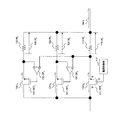
図6に特許文献1に開示された並列接続FET回路の回路図を示す。
FIG. 6 shows a circuit diagram of a parallel-connected FET circuit disclosed in
図6に示すように、並列に接続された各FET(FET2〜FETn)には、ゲート・ソース間電圧を制御するオペアンプ(OP2〜OPn)が個々に接続される。そして、各オペアンプ(OP2〜OPn)は、各FETのソース側に接続された各抵抗(Rf2〜Rfn)の両端に生じる電位差(Vf2〜Vfn)が同じになるように動作し、その結果、各FETに流れる電流量(i1〜in)は等しくなる。 As shown in FIG. 6, operational amplifiers (OP 2 to OP n ) for controlling the gate-source voltage are individually connected to the FETs (FET 2 to FET n ) connected in parallel. The operational amplifiers (OP 2 to OP n ) operate so that the potential differences (Vf 2 to Vf n ) generated at both ends of the resistors (Rf 2 to Rf n ) connected to the source side of the FETs are the same. As a result, the amount of current (i 1 to i n ) flowing through each FET becomes equal.
一般に、FET、バイポーラトランジスタ等の増幅素子を用いた増幅器は、増幅素子に印加されるバイアスの量によってA級、AB級、B級等に分類される。 In general, an amplifier using an amplifying element such as an FET or a bipolar transistor is classified into A class, AB class, B class, and the like depending on the amount of bias applied to the amplifying element.
このうち、AB級増幅器やB級増幅器では、増幅素子に印加するバイアス量を大きくすると、その増幅素子に大きな動作電流が流れるので消費電力が増加し、電力効率が低下する。一方、増幅素子に印加するバイアス量を小さくしすぎると、クロスオーバー歪による非線形歪が発生する。 Among these, in the class AB amplifier and the class B amplifier, when the bias amount applied to the amplifying element is increased, a large operating current flows through the amplifying element, so that the power consumption increases and the power efficiency decreases. On the other hand, if the bias amount applied to the amplifying element is too small, nonlinear distortion due to crossover distortion occurs.
従って、AB級増幅器またはB級増幅器が並列に動作する電力増幅装置に、特許文献1に記載の技術を適用して各増幅器に流れる電流量を同一にしても、印加するバイアス量が大きすぎると電力効率が低下し、バイアス量が小さすぎると非線形歪が発生するという問題があった。
Accordingly, even if the amount of current flowing through each amplifier is the same by applying the technique described in
また、A級増幅器が並列に動作する電力増幅装置に、特許文献1に記載の技術を適用して各増幅器に流れる電流量を同一にした場合も、印加するバイアス量が適切な大きさでないと増幅特性の線形領域が狭くなり、出力信号の線形性(入力信号に対する比例性)が低下するという問題があった。
In addition, even when the amount of current flowing through each amplifier is made the same by applying the technique described in
本発明の目的は、並列に接続された増幅器群を備える電力増幅装置において、非線形歪の発生を抑制しつつ、並列接続された増幅器群での電力効率の低下を抑制するための技術を提供することである。 An object of the present invention is to provide a technique for suppressing a decrease in power efficiency in an amplifier group connected in parallel while suppressing occurrence of nonlinear distortion in a power amplifying apparatus including the amplifier group connected in parallel. That is.
上記目的を達成するために、本発明の電力増幅装置は、入力信号を所望の電力に増幅する電力増幅装置であって、
複数の増幅器を並列に接続した増幅器群と、
入力信号を分配して前記複数の増幅器に供給する分配手段と、
前記複数の増幅器の出力信号を合成する合成手段と、
各増幅器の増幅素子へ個別にバイアスをかけるバイアス印加手段と、
各増幅器の増幅素子に流れる電流量を測定する電流検出手段と、
前記合成手段によって合成された信号に含まれる非線形歪を測定する歪検出手段と、
前記電流検出手段から各増幅器の増幅素子に流れる電流量を示す情報を取得すると共に、前記歪検出手段から前記非線形歪の測定値を取得し、各増幅器の増幅素子の前記電流量が同一となり、前記非線形歪の測定値が予め定められた範囲に収まるように、前記バイアス印加手段が各増幅器の増幅素子へ印加するバイアス量を調整する制御手段と、
を有する。
In order to achieve the above object, a power amplification device of the present invention is a power amplification device that amplifies an input signal to a desired power,
An amplifier group in which a plurality of amplifiers are connected in parallel;
Distributing means for distributing an input signal to supply the plurality of amplifiers;
Combining means for combining the output signals of the plurality of amplifiers;
Bias applying means for individually biasing the amplifying element of each amplifier;
Current detection means for measuring the amount of current flowing through the amplification element of each amplifier;
Distortion detection means for measuring nonlinear distortion included in the signal synthesized by the synthesis means;
While obtaining information indicating the amount of current flowing through the amplification element of each amplifier from the current detection means, obtaining a measurement value of the nonlinear distortion from the distortion detection means, the current amount of the amplification element of each amplifier becomes the same, Control means for adjusting the amount of bias applied by the bias applying means to the amplifying element of each amplifier so that the measured value of the nonlinear distortion falls within a predetermined range;
Have
また、上記目的を達成するために、本発明の制御方法は、並列に接続された複数の増幅器を備える電力増幅装置の制御方法であって、
各増幅器の増幅素子に流れる電流量を測定し、
前記電力増幅装置の出力信号に含まれる非線形歪を測定し、
各増幅器の増幅素子の前記電流量が同一となり、前記非線形歪の測定値が予め定められた範囲に収まるように、各増幅器の増幅素子へ印加するバイアス量を個別に調整する。
In order to achieve the above object, a control method of the present invention is a control method of a power amplifying apparatus including a plurality of amplifiers connected in parallel,
Measure the amount of current flowing through the amplifier element of each amplifier,
Measure nonlinear distortion included in the output signal of the power amplifier,
The amount of bias applied to the amplifying element of each amplifier is individually adjusted so that the amount of current of the amplifying element of each amplifier becomes the same and the measured value of the nonlinear distortion falls within a predetermined range.
本発明によれば、並列に接続された増幅器群を備える電力増幅装置において、非線形歪の発生を抑制しつつ、並列接続された増幅器群での電力効率の低下を抑制できる。 ADVANTAGE OF THE INVENTION According to this invention, in a power amplification apparatus provided with the amplifier group connected in parallel, the fall of the power efficiency in the amplifier group connected in parallel can be suppressed, suppressing generation | occurrence | production of nonlinear distortion.
次に本発明について図面を参照して詳細に説明する。 Next, the present invention will be described in detail with reference to the drawings.
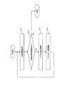
(第1の実施の形態)
図1は第1の実施の形態の電力増幅装置の構成を示す図である。
(First embodiment)
FIG. 1 is a diagram illustrating a configuration of the power amplifying device according to the first embodiment.
図1に示すように、本実施形態の電力増幅装置1は、増幅処理部10と、歪補償器30と、方向性結合器33を有する。なお、電力増幅装置1は、歪特性を良好にするために、飽和出力値から十分にマージン(バックオフ)を取った、線形性の高い出力レベルで使用される。
As illustrated in FIG. 1, the power amplifying
増幅処理部10は、複数の増幅器を並列に接続して入力信号を所望の電力に増幅する機能を備え、可変アッテネータ11と、ドライブアンプ12と、入力検波器13と、増幅器並列構成段14と、出力検波器18と、CPU(Central Processing Unit)19と、バイアス印加部20と、電流検出器21と、電圧供給部22を有する。
The amplification processing unit 10 has a function of amplifying an input signal to a desired power by connecting a plurality of amplifiers in parallel, and includes a
可変アッテネータ11は、外部から入力された信号を適切なレベルに減衰させる周知の減衰器である。
The
ドライブアンプ12は、可変アッテネータ11から出力された信号を適切なレベルに増幅して増幅器並列構成段14に供給する。
The
増幅器並列構成段14は、分配器15と、第1の増幅器161〜第nの増幅器16nと、合成器17を有する。なお、本実施形態の各増幅器は、FETで構成された、AB級増幅器またはB級増幅器である。
The amplifier
増幅器並列構成段14では、ドライブアンプ12から出力された信号を分配器15が分配して第1の増幅器161〜第nの増幅器16nに供給し、分配器15によって分配された各信号を第1の増幅器161〜第nの増幅器16nが増幅し、各増幅器によって増幅された信号を合成器17が合成して外部に出力する。
In the amplifier
入力検波器13は、増幅器並列構成段14に入力される信号のレベルを検出し、入力信号のレベルを示す入力レベル情報をCPU19からの取得要求に応じて通知する。
The
一方、出力検波器18は、増幅器並列構成段14から出力された信号(つまり、電力増幅装置1の出力信号)のレベルを検出し、出力信号のレベルを示す出力レベル情報をCPU19からの取得要求に応じて通知する。
On the other hand, the
バイアス印加部20は、第1の増幅器161〜第nの増幅器16nの増幅素子に個別にバイアスをかける装置であり、本実施形態のバイアス印加部20は、各増幅器のFETにバイアス電圧Vg1〜Vgnを供給し、CPU19からのバイアス制御信号に応じてバイアス電圧Vg1〜Vgnの大きさを変更する。例えば、バイアス印加部20は、CPU19からの制御信号をアナログ信号に変換するD/A(デジタル/アナログ)変換器によって実現される。
The
電圧供給部22は、電流検出器21を介して、第1の増幅器161〜第nの増幅器16nの増幅素子の出力端子に電源電圧を供給する電源装置であり、本実施形態の電圧供給部22は、各増幅器のFETのドレイン端子にドレイン電圧Vdを供給し、CPU19からの電圧制御信号に応じてドレイン電圧Vdの大きさを変更する。
The
電流検出器21は、第1の増幅器161〜第nの増幅器16nの増幅素子にそれぞれ流れる電流量を測定する検出器であり、本実施形態の電流検出器21は、各増幅器のFETに流れるドレイン電流(以降、動作電流と称する)の電流量(以降、動作電流量と称する)Id1〜Idnを測定し、測定した動作電流量を示す電流量情報をCPU19からの取得要求に応じて通知する。
The
方向性結合器33は、増幅処理部10の出力信号を取り出して歪補償器30へ供給する。
The
歪補償器30は、外部から入力された原信号を補正して増幅処理部10へ出力する機能を備え、補正部31および歪検出部32を有する。なお、補正部31および歪検出部32は、例えば論理回路等から構成されるLSI(Large Scale Integration)あるいはプログラムにしたがって動作するCPUやDSP(Digital Signal Processor)等によって実現される。
The distortion compensator 30 has a function of correcting an original signal input from the outside and outputting it to the amplification processing unit 10, and includes a
歪検出部32は、方向性結合器33から供給された、増幅処理部10の出力信号に含まれる非線形歪を測定する検出器であり、本実施形態の歪検出部32は、増幅処理部10の出力信号に含まれる相互変調歪を示すIM(inter-modulation distortion)値を測定し、測定したIM値を示すIM値情報を補正部31に通知すると共に、CPU19からの取得要求に応じてCPU19にも通知する。なお、相互変調歪は、近接した2つの周波数成分の間で生じる新たな周波数成分による歪であり、出力信号に非線形性がある(入力信号に対して完全に比例しない)場合に発生する。また、IM値の測定方法は、例えば特開2005−244430号に記載されているため、ここでは詳細な説明を省略する。
The
補正部31は、歪検出部32が測定するIM値が最良の値となるように、方向性結合器33から供給された、増幅処理部10の出力信号を用いて、外部から入力された原信号を補正して増幅処理部10へ出力する。
The
CPU19は、入力検波器13、出力検波器18、電流検出器21ならびに歪検出部32から入力レベル情報、出力レベル情報、各増幅器の電流量情報ならびにIM値情報をそれぞれ取得し、取得した情報に基づいて、可変アッテネータ11の減衰量、バイアス印加部20が各増幅器のFETに供給するバイアス電圧ならびに電圧供給部22が各増幅器のFETに供給するドレイン電圧を調整する制御装置である。
The
以下に、本実施形態の電力増幅装置1の動作の概略について説明する。
Below, the outline | summary of operation | movement of the
まず、電力増幅装置1では、増幅器並列構成段14の電力効率の低下を抑制するため、各増幅器の出力レベルを同一にし、合成器17での合成損失を低減する必要がある。そして、本実施形態の第1の増幅器161〜第nの増幅器16nは、FETで構成された、AB級増幅器またはB級増幅器であるため、各増幅器のFETに印加するバイアス電圧Vg1〜Vgnを変更することにより、各FETに流れる動作電流量Id1〜Idnを調整して各増幅器の出力レベルを同一にすることができる。
First, in the
なお、電力増幅装置1への信号が未入力の状態で各FETに流れるドレイン電流(以降、アイドル電流と称する)の量が全てのFETで同一になるように、各FETへ印加するバイアス電圧を調整することも可能であるが、FETは個体差が大きく、利得にばらつきがあるため、アイドル電流が同一になるように各FETを調整しても、電力増幅装置1を定格出力にした時に各FETに流れるドレイン電流(動作電流)が同一になるとは限らない。
In addition, the bias voltage applied to each FET is set so that the amount of drain current (hereinafter referred to as idle current) flowing through each FET when no signal is input to the
そこで、本実施形態では、CPU19は、電力増幅装置1の出力レベルが定格出力となるように可変アッテネータ11の減衰量を調整した状態で、各FETに流れる動作電流量Id1〜Idnを電流検出器21から取得し、各動作電流量が同一になるように、バイアス制御信号を用いて、バイアス印加部20が各FETに印加するバイアス電圧Vg1〜Vgnを調整する。
Therefore, in this embodiment,
なお、各FETに印加するバイアス電圧Vg1〜Vgnを変更すると、各FETの利得が変動し、電力増幅装置1の利得も変動する。そのため、電力増幅装置1の出力レベルが定格出力から外れるので、CPU19は、出力検波器18から出力レベル情報を取得し、電力増幅装置1の出力レベルが定格出力となるように可変アッテネータ11の減衰量を再調整する。
Incidentally, by changing the bias voltage Vg 1 through Vg n to be applied to each FET, the gain of each FET is varied, also varied gain of the
また、電力効率は消費電力に対する出力電力の比率であるので、増幅器並列構成段14の電力効率の低下を抑制するためには、各FETの消費電力を低減することが重要である。そして、AB級増幅器やB級増幅器では、FETに印加するバイアス電圧を低減すると、そのFETに流れる動作電流量が減少するので、消費電力を低減できる。なお、電力増幅装置1の消費電力の大部分は、増幅器並列構成段14の各増幅器のFETで消費されるので、各FETの消費電力を低減することにより、電力増幅装置1全体の消費電力も低減できる。
In addition, since the power efficiency is the ratio of the output power to the power consumption, it is important to reduce the power consumption of each FET in order to suppress the reduction in the power efficiency of the amplifier
そこで、CPU19は、各FETに流れる動作電流量Id1〜Idnを低減するようにバイアス電圧Vg1〜Vgnを調整する。
Therefore,
一方、AB級増幅器やB級増幅器では、FETに印加するバイアス電圧を低減しすぎると、クロスオーバー歪による非線形歪が発生する。そこで、出力信号の線形性を確保するようにIM値の許容範囲を予め定めておき、CPU19は、その許容範囲にIM値が収まるようにバイアス電圧Vg1〜Vgnを調整する。
On the other hand, in the class AB amplifier and the class B amplifier, if the bias voltage applied to the FET is excessively reduced, nonlinear distortion due to crossover distortion occurs. Therefore, the allowable range of IM value to ensure the linearity of the output signal determined in advance for,
また、電力増幅装置1のバックオフ量が十分に大きい場合、増幅器並列構成段14の各増幅器のFETに供給するドレイン電圧を低減することによって、各FETの消費電力を低減してもよい。一方、ドレイン電圧を低減すると、各FETの飽和出力値が小さくなり、バックオフ量が小さくなるため、ドレイン電圧を低減しすぎると、出力信号の線形性が低下する。そこで、CPU19は、出力信号の線形性を確保するように定められた許容範囲にIM値が収まる条件下で、各FETに供給するドレイン電圧Vdを低減するように、電圧制御信号を用いて電圧供給部22を制御する。
Further, when the back-off amount of the
なお、ドレイン電圧Vdを変更する場合も、CPU19は、出力検波器18から出力レベル情報を取得し、電力増幅装置1の出力レベルが定格出力となるように可変アッテネータ11の減衰量を調整する。
Even when the drain voltage Vd is changed, the
次に図1に示した電力増幅装置1が各増幅器の出力レベルを同一にするときの処理手順について、図2に示すフローチャートを用いて説明する。
Next, a processing procedure when the
図2に示すように、電力増幅装置1のCPU19は、まず、電力増幅装置1へ信号が入力されていない状態で第1の増幅器161〜第nの増幅器16nの各FETに流れるアイドル電流の量が全てのFETで同一になるように、バイアス制御信号を用いて、バイアス印加部20が各FETに印加するバイアス電圧Vg1〜Vgnを調整する(ステップS1)。
As shown in FIG. 2, the
全てのFETに流れるアイドル電流の量が同一になるように調整すると、CPU19は、入力検波器13から入力レベル情報を取得して増幅器並列構成段14に信号が入力されているか否かを判定し、増幅器並列構成段14に信号が入力されるまで待機する。そして、増幅器並列構成段14に信号が入力されると、CPU19は、出力検波器18から出力レベル情報を取得して電力増幅装置1の出力レベルを判別し、電力増幅装置1が定格出力になるように可変アッテネータ11の減衰量を制御する(ステップS2)。
When adjustment is made so that the amount of idle current flowing through all FETs is the same, the
電力増幅装置1を定格出力にすると、CPU19は、電力増幅装置1の定格出力時に第1の増幅器161〜第nの増幅器16nの各FETに流れる動作電流の電流量情報を電流検出器21から取得する。そして、CPU19は、各FETの動作電流量が予め設定された電流量になるように、バイアス制御信号を用いてバイアス電圧Vg1〜Vgnを調整する(ステップS3)。なお、動作電流量が予め設定された電流量より少ないFETに対しては印加するバイアス電圧を増加し、動作電流量が予め設定された電流量より多いFETに対しては印加するバイアス電圧を低減することにより、CPU19は、各FETの動作電流量が同一になるように調整し、各増幅器の出力レベルを同一にする。
When the
一方、各FETに印加するバイアス電圧を変更すると、各FETの利得が変動し、電力増幅装置1の出力レベルが定格出力から外れる。そのため、CPU19は、出力検波器18から出力レベル情報を取得し、電力増幅装置1の出力レベルが定格出力となるように可変アッテネータ11の減衰量を再調整する。その後、CPU19は、入力検波器13から入力レベル情報を取得し、出力検波器18から出力レベル情報を取得する。そして、CPU19は、入力レベル情報と出力レベル情報から増幅器並列構成段14の利得を算出し、算出した利得が予め定められた範囲にあるか否かを判定する(ステップS4)。
On the other hand, when the bias voltage applied to each FET is changed, the gain of each FET varies, and the output level of the
増幅器並列構成段14の利得が予め定められた範囲にない場合、CPU19は、再度、バイアス制御信号を用いてバイアス電圧Vg1〜Vgnを調整する(ステップS5)。例えば、増幅器並列構成段14の利得が大きい場合、CPU19は、バイアス電圧Vg1〜Vgnを低減することにより、各FETの動作電流量を減少させて出力レベルを減少させる。一方、増幅器並列構成段14の利得が小さい場合、CPU19は、バイアス電圧Vg1〜Vgnを増加することにより、各FETの動作電流量を増加させて出力レベルを増加させる。なお、この場合も、ステップS3の処理と同様に、CPU19は、各FETの動作電流量が同一になるようにバイアス電圧Vg1〜Vgnを調整する。
If not in the range where the gain of the amplifier
そして、バイアス電圧Vg1〜Vgnを再調整すると、CPU19は、再度、ステップS4へ移行して、増幅処理部10の出力レベルが定格出力となるように可変アッテネータ11の減衰量を調整し、増幅器並列構成段14の利得が予め定められた範囲にあるか否かを判定する。
When readjusting the bias voltage Vg 1 through Vg n, CPU 19 again, the operation proceeds to Step S4, the output level of the amplifier unit 10 adjusts the attenuation of the
一方、増幅器並列構成段14の利得が予め定められた範囲に入ると、CPU19は、バイアス電圧の調整処理を終了する。
On the other hand, when the gain of the amplifier
次に図1に示した電力増幅装置1が出力信号のIM値に基づいて各FETに印加するバイアス電圧を調整するときの処理手順について、図3に示すフローチャートを用いて説明する。
Next, the processing procedure when the
なお、図3に示したフローチャートでは、電力増幅装置1には、出力信号の線形性を確保するようにIM値の許容範囲(最小値〜最大値)が予め設定されているものとする。また、図3に示した処理の開始前に、図2に示した処理により、電力増幅装置1は、定格出力時の各増幅器の出力レベルが同一になるように調整しているものとする。
In the flowchart shown in FIG. 3, it is assumed that an allowable range (minimum value to maximum value) of the IM value is set in advance in the
また、歪補償器30には、常時、方向性結合器33によって取り出された増幅処理部10の出力信号が入力される。そして、歪検出部32は、増幅処理部10の出力信号のIM値を測定して補正部31に通知する。一方、補正部31は、歪検出部32が測定するIM値が最良の値となるように、方向性結合器33から供給された、増幅処理部10の出力信号を用いて、外部から入力された原信号を補正して増幅処理部10へ出力する。
The distortion compensator 30 is always supplied with the output signal of the amplification processing unit 10 taken out by the
図3に示すように、CPU19は、まず、歪検出部32から増幅処理部10の出力信号のIM値情報を取得し(ステップS11)、増幅処理部10の出力信号のIM値が許容範囲に収まっているか否かを判別する(ステップS12)。
As shown in FIG. 3, the
IM値が許容範囲に収まっている場合、CPU19は、バイアス電圧の調整処理を終了する。
When the IM value is within the allowable range, the
一方、IM値が許容範囲に収まっていない場合、CPU19は、IM値が許容範囲に収まるように、バイアス制御信号を用いてバイアス電圧Vg1〜Vgnを調整する(ステップS13)。なお、CPU19は、IM値が許容範囲より良好な値を示す(出力信号の相互変調歪が小さい)場合、歪特性に余裕があるので、各FETに印加するバイアス電圧を全体的に低減させて増幅器並列構成段14の電力効率を高める。一方、CPU19は、IM値が許容範囲より悪い値を示す(出力信号の相互変調歪が大きい)場合、各FETに印加するバイアス電圧を全体的に増加させて出力電力の線形性を高め、歪特性を良好にする。また、このとき、CPU19は、図2のステップS3の処理と同様に各FETの動作電流量が同一になるようにバイアス電圧Vg1〜Vgnを調整する。
On the other hand, if the IM value is not within the allowable range,
各FETに印加するバイアス電圧を変更すると、各FETの利得が変動し、電力増幅装置1の出力レベルが定格出力から外れる。そのため、CPU19は、出力検波器18から出力レベル情報を取得し、増幅処理部10の出力レベルが定格出力となるように可変アッテネータ11の減衰量を再調整する(ステップS14)。
When the bias voltage applied to each FET is changed, the gain of each FET varies, and the output level of the
可変アッテネータ11の減衰量を再調整すると、CPU19は、再度、ステップS11へ移行して、歪検出部32から増幅処理部10の出力信号のIM値情報を取得し、増幅処理部10の出力信号のIM値が許容範囲に収まっているか否かを判別する(ステップS12)。
When the attenuation amount of the
次に図1に示した電力増幅装置1が出力信号のIM値に基づいてドレイン電圧を調整するときの処理手順について、図4に示すフローチャートを用いて説明する。
Next, a processing procedure when the
なお、図4に示したフローチャートでは、電力増幅装置1には、予め出力信号のIM値の許容範囲が設定されているものとする。また、図4に示した処理の開始前に、図3に示した処理により、電力増幅装置1は、出力信号のIM値に基づいて各FETに印加するバイアス電圧を調整しており、出力信号のIM値は、許容範囲に収まっているものとする。
In the flowchart shown in FIG. 4, it is assumed that the allowable range of the IM value of the output signal is set in advance in the
また、図3に示した処理と同様に、電力増幅装置1の歪補償器30には、常時、方向性結合器33によって取り出された増幅処理部10の出力信号が入力される。そして、歪検出部32は、増幅処理部10の出力信号のIM値を測定して補正部31に通知する。一方、補正部31は、歪検出部32が測定するIM値が最良の値となるように、方向性結合器33から供給された、増幅処理部10の出力信号を用いて、外部から入力された原信号を補正して増幅処理部10へ出力する。
Similarly to the processing shown in FIG. 3, the distortion compensator 30 of the
図4に示すように、CPU19は、まず、各FETに供給するドレイン電圧Vdを低減するように、電圧制御信号を用いて電圧供給部22を制御する(ステップS21)。
As shown in FIG. 4, the
各FETに供給するドレイン電圧Vdを変更すると、CPU19は、出力検波器18から出力レベル情報を取得し、電力増幅装置1の出力レベルが定格出力となるように可変アッテネータ11の減衰量を再調整する(ステップS22)。
When the drain voltage Vd supplied to each FET is changed, the
可変アッテネータ11の減衰量を再調整すると、CPU19は、歪検出部32から増幅処理部10の出力信号のIM値情報を取得し(ステップS23)、増幅処理部10の出力信号のIM値が許容範囲に収まっているか否かを判別する(ステップS24)。
When the attenuation amount of the
IM値が許容範囲に収まっている場合、CPU19は、再度、ステップS21へ移行して、各FETに供給するドレイン電圧Vdをさらに低減するように、電圧制御信号を用いて電圧供給部22を制御する。
When the IM value is within the allowable range, the
一方、IM値が許容範囲に収まっていない場合、CPU19は、各FETに供給するドレイン電圧Vdを、直前に設定していた電圧値に戻し(ステップS25)、ドレイン電圧の調整処理を終了する。
On the other hand, if the IM value is not within the allowable range, the
なお、本実施形態では、各増幅器がFETで構成される例を示したが、本発明はこれに限定されるものではなく、例えば、各増幅器はバイポーラトランジスタで構成されるものでもよい。この場合、電流検出器21は、各増幅器のバイポーラトランジスタに流れるコレクタ電流量を測定してCPU19にコレクタ電流量を示す情報を通知すればよい。そして、バイアス印加部20は、各バイポーラトランジスタに個別にバイアス電流を流し、CPU19からのバイアス制御信号に応じて各バイポーラトランジスタへ流すバイアス電流量を変更すればよい。また、電圧供給部22は、各バイポーラトランジスタのコレクタ端子にコレクタ電圧を供給し、CPU19からの電圧制御信号に応じてコレクタ電圧を変更すればよい。
In the present embodiment, an example in which each amplifier is configured by an FET is shown. However, the present invention is not limited to this. For example, each amplifier may be configured by a bipolar transistor. In this case, the
また、本実施形態では、各増幅器がAB級増幅器またはB級増幅器である例を示したが、本発明はこれに限定されるものではなく、例えば、各増幅器はA級増幅器でもよい。この場合も、電力増幅装置1は、各FETの動作電流量が同一となり、かつ、IM値が予め定められた範囲に収まるように、各FETへ印加するバイアス電圧を調整すればよく、さらに、IM値が予め定められた範囲に収まる条件下でドレイン電圧を低減すればよい。
Further, in this embodiment, an example in which each amplifier is a class AB amplifier or a class B amplifier is shown, but the present invention is not limited to this, and for example, each amplifier may be a class A amplifier. In this case as well, the
また、本実施形態では、電力増幅装置1は、出力信号の相互変調歪を測定し、その相互変調歪が予め定められた範囲に収まるように、各FETへ印加するバイアス電圧や各FETへ供給するドレイン電圧を調整する例を示したが、本発明はこれに限定されるものではない。バイアス電圧やドレイン電圧を調整するために参照する情報は非線形歪を示す情報ならどのようなものでもよく、例えば、電力増幅装置1は、出力信号の高調波歪を測定し、その高調波歪が予め定められた範囲に収まるように、各FETへ印加するバイアス電圧を調整してもよい。
In the present embodiment, the
また、本実施形態では、電力増幅装置1を定格出力にした状態で、各FETへ印加するバイアス電圧を調整する例を示したが、本発明はこれに限定されるものではない。電力増幅装置1の動作時の各増幅器の出力レベルを同一にするためには、電力増幅装置1の出力レベルを可能な限り大きくした状態でバイアス電圧を調整することが望ましいが、必ずしも電力増幅装置1を定格出力にする必要はない。例えば、バイアス電圧を調整するときの出力レベルを予め定めておき、電力増幅装置1の出力レベルをその定められたレベルにした状態でバイアス電圧を調整してもよい。
In the present embodiment, the example in which the bias voltage applied to each FET is adjusted in a state where the
また、例えば、電力増幅装置1は、常時、各FETに流れる動作電流量と出力信号のIM値を測定し、各FETの動作電流量が同一となり、IM値が予め定められた範囲に収まるように、各FETへ印加するバイアス電圧を調整してもよい。その場合、電力増幅装置1は、可変アッテネータ11の減衰量を調整して出力レベルを変更することなく、バイアス電圧を調整してよい。
Further, for example, the
また、本実施形態では、電力増幅装置1を定格出力にした状態で、各FETへ供給するドレイン電圧を低減する例を示したが、本発明はこれに限定されるものではない。例えば、ドレイン電圧を調整するときの出力レベルを予め定めておき、電力増幅装置1の出力レベルをその定められたレベルにした状態でドレイン電圧を調整してもよい。この場合、電力増幅装置1は、その定められたレベル以下の出力レベルで動作するときの出力信号の線形性を確保できる。
Moreover, in this embodiment, although the example which reduces the drain voltage supplied to each FET in the state which made the
以上説明したように、本実施形態によれば、電力増幅装置は、並列に接続された複数の増幅器を備え、各増幅器の増幅素子に流れる動作電流量が同一となり、出力信号の非線形歪の測定値が予め定められた範囲に収まるように、各増幅器の増幅素子へ印加するバイアス量を調整する。 As described above, according to the present embodiment, the power amplifying apparatus includes a plurality of amplifiers connected in parallel, the amount of operating current flowing through the amplifying elements of each amplifier is the same, and measurement of nonlinear distortion of the output signal The amount of bias applied to the amplification element of each amplifier is adjusted so that the value falls within a predetermined range.
これにより、電力増幅装置は、各増幅器の出力レベルを同一に保ちつつ、非線形歪が十分に小さい(良好な)場合、バイアス量を低減して各増幅器の電力消費を抑制し、非線形歪が大きい(悪い)場合、バイアス量を増加して出力信号の歪特性を良好にする。従って、並列に接続された複数の増幅器を備える電力増幅装置において、非線形歪の発生を抑制しつつ、並列接続された増幅器群での電力効率の低下を抑制できる。 As a result, the power amplifying apparatus reduces the bias amount and suppresses the power consumption of each amplifier when the nonlinear distortion is sufficiently small (good) while keeping the output level of each amplifier the same, and the nonlinear distortion is large. In the case of (bad), the bias amount is increased to improve the distortion characteristics of the output signal. Therefore, in a power amplifying apparatus including a plurality of amplifiers connected in parallel, it is possible to suppress a decrease in power efficiency in the amplifier group connected in parallel while suppressing the occurrence of nonlinear distortion.
また、本実施形態の電力増幅装置は、自装置の出力レベルを予め定められたレベルにした状態で、各増幅器の増幅素子へ印加するバイアス量を調整する。これにより、電力増幅装置は、各増幅器の増幅素子へ印加するバイアス量の調整処理を常時実施しなくても、動作時の各増幅器の出力レベルのばらつきを抑制できるので、バイアス量の調整処理による処理負荷の増大を抑制しつつ、並列接続された増幅器群での電力効率の低下を抑制できる。 In addition, the power amplifying apparatus according to the present embodiment adjusts the bias amount applied to the amplifying element of each amplifier in a state where the output level of the apparatus is set to a predetermined level. As a result, the power amplifying apparatus can suppress variations in the output level of each amplifier during operation without always performing adjustment processing of the bias amount applied to the amplification element of each amplifier. While suppressing an increase in processing load, a decrease in power efficiency in the amplifier group connected in parallel can be suppressed.
また、本実施形態の電力増幅装置は、自装置の出力レベルを予め定められた出力レベルにした状態で、出力信号の非線形歪の測定値が予め定められた範囲に収まる条件下で各増幅器の増幅素子の出力端子へ供給する電圧を低減する。これにより、電力増幅装置は、各増幅素子へ供給する電圧の調整処理を常時実施することなく、その定められた出力レベルで動作する場合の出力信号の線形性を確保しつつ、各増幅素子へ供給する電圧を低減できる。従って、電力増幅装置は、予め定められた出力レベルで動作する場合、各増幅素子へ供給する電圧の調整処理による処理負荷の増大を抑制しつつ、出力信号の線形性を確保すると共に各増幅器の消費電力の増大を抑制できる。 In addition, the power amplifying apparatus according to the present embodiment has the output level of the self-apparatus set to a predetermined output level, and the measured value of the nonlinear distortion of the output signal falls within a predetermined range. The voltage supplied to the output terminal of the amplifying element is reduced. As a result, the power amplifying device does not always perform the adjustment process of the voltage supplied to each amplifying element, and ensures the linearity of the output signal when operating at the determined output level. The supplied voltage can be reduced. Therefore, when the power amplifying device operates at a predetermined output level, it suppresses an increase in processing load due to adjustment processing of the voltage supplied to each amplifying element, while ensuring linearity of the output signal and each amplifier. An increase in power consumption can be suppressed.
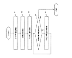
(第2の実施の形態)
図5は、第2の実施の形態の電力増幅装置の構成を示す図である。
(Second Embodiment)
FIG. 5 is a diagram illustrating a configuration of the power amplification device according to the second embodiment.
図5に示すように、本実施形態の電力増幅装置1は、第1の増幅器161〜第nの増幅器16nを並列に接続した増幅器群と、入力信号を分配して第1の増幅器161〜第nの増幅器16nに供給する分配器15と、第1の増幅器161〜第nの増幅器16nの出力信号を合成する合成器17と、第1の増幅器161〜第nの増幅器16nの増幅素子へ個別にバイアスをかけるバイアス印加部20と、電流検出器21は第1の増幅器161〜第nの増幅器16nの増幅素子に流れる動作電流量を測定する電流検出器21と、合成器17が合成した信号に含まれる非線形歪を測定する歪検出部32と、CPU19を有する。
As shown in FIG. 5, the
そして、CPU19は、電流検出器21から各増幅器の増幅素子に流れる動作電流量を示す情報を取得すると共に、歪検出部32から非線形歪の測定値を取得し、各増幅器の増幅素子の動作電流量が同一となり、非線形歪の測定値が予め定められた範囲に収まるように、バイアス印加部20が各増幅器の増幅素子へ印加するバイアス量を調整する。
Then, the
以上、第2の実施の形態においても、並列に接続された複数の増幅器を備える電力増幅装置は、非線形歪の発生を抑制しつつ、並列接続された増幅器群での電力効率の低下を抑制できる。 As described above, also in the second embodiment, a power amplifying apparatus including a plurality of amplifiers connected in parallel can suppress a decrease in power efficiency in a group of amplifiers connected in parallel while suppressing the occurrence of nonlinear distortion. .
1 電力増幅装置
10 増幅処理部
11 可変アッテネータ
12 ドライブアンプ
13 入力検波器
14 増幅器並列構成段
15 分配器
161 第1の増幅器
162 第2の増幅器
163 第3の増幅器
16n 第nの増幅器
17 合成器
18 出力検波器
19 CPU
20 バイアス印加部
21 電流検出器
22 電圧供給部
30 歪補償器
31 補正部
32 歪検出部
33 方向性結合器
111 FET1
112 電源制御部
113 Rf1
114 i1
115 Vf1
121 FET2
122 OP2
123 Rf2
124 i2
125 Vf2
131 FETn
132 OPn
133 Rfn
134 in
135 Vfn
144 I
DESCRIPTION OF
20
112
114 i 1
115 Vf 1
121 FET 2
122 OP 2
123 Rf 2
124 i 2
125 Vf 2
131 FET n
132 OP n
133 Rf n
134 i n
135 Vf n
144 I
Claims (6)
複数の増幅器を並列に接続した増幅器群と、
入力信号を分配して前記複数の増幅器に供給する分配手段と、
前記複数の増幅器の出力信号を合成する合成手段と、
各増幅器の増幅素子へ個別にバイアスをかけるバイアス印加手段と、
各増幅器の増幅素子に流れる電流量を測定する電流検出手段と、
前記合成手段によって合成された信号に含まれる非線形歪を測定する歪検出手段と、
前記電流検出手段から各増幅器の増幅素子に流れる電流量を示す情報を取得すると共に、前記歪検出手段から前記非線形歪の測定値を取得し、各増幅器の増幅素子の前記電流量が同一となり、前記非線形歪の測定値が予め定められた範囲に収まるように、前記バイアス印加手段が各増幅器の増幅素子へ印加するバイアス量を調整する制御手段と、
を有する電力増幅装置。 A power amplification device that amplifies an input signal to a desired power,
An amplifier group in which a plurality of amplifiers are connected in parallel;
Distributing means for distributing an input signal to supply the plurality of amplifiers;
Combining means for combining the output signals of the plurality of amplifiers;
Bias applying means for individually biasing the amplifying element of each amplifier;
Current detection means for measuring the amount of current flowing through the amplification element of each amplifier;
Distortion detection means for measuring nonlinear distortion included in the signal synthesized by the synthesis means;
While obtaining information indicating the amount of current flowing through the amplification element of each amplifier from the current detection means, obtaining a measurement value of the nonlinear distortion from the distortion detection means, the current amount of the amplification element of each amplifier becomes the same, Control means for adjusting the amount of bias applied by the bias applying means to the amplifying element of each amplifier so that the measured value of the nonlinear distortion falls within a predetermined range;
A power amplifying apparatus.
前記制御手段は、電力増幅装置の出力信号のレベルを予め定められたレベルにした状態で前記バイアス量を調整することを特徴とする電力増幅装置。 The power amplifying device according to claim 1,
The control means adjusts the bias amount in a state where the level of the output signal of the power amplifying apparatus is set to a predetermined level.
前記複数の増幅器の増幅素子の出力端子へ電圧を供給する電圧供給手段をさらに有し、
前記制御手段は、電力増幅装置の出力信号のレベルを予め定められたレベルにした状態で、前記非線形歪の測定値が前記予め定められた範囲に収まる条件下で前記電圧供給手段が供給する電圧を低減するように該電圧供給手段を制御することを特徴とする電力増幅装置。 In the power amplification device according to claim 2,
Voltage supply means for supplying a voltage to the output terminals of the amplifying elements of the plurality of amplifiers;
The control means is a voltage supplied by the voltage supply means under the condition that the measured value of the nonlinear distortion falls within the predetermined range in a state where the level of the output signal of the power amplification device is set to a predetermined level. A power amplifying apparatus that controls the voltage supply means so as to reduce the noise.
各増幅器の増幅素子に流れる電流量を測定し、
前記電力増幅装置の出力信号に含まれる非線形歪を測定し、
各増幅器の増幅素子の前記電流量が同一となり、前記非線形歪の測定値が予め定められた範囲に収まるように、各増幅器の増幅素子へ印加するバイアス量を個別に調整する制御方法。 A method for controlling a power amplifying apparatus comprising a plurality of amplifiers connected in parallel,
Measure the amount of current flowing through the amplifier element of each amplifier,
Measure nonlinear distortion included in the output signal of the power amplifier,
A control method for individually adjusting the amount of bias applied to the amplifying element of each amplifier so that the current amount of the amplifying element of each amplifier is the same and the measured value of the nonlinear distortion is within a predetermined range.
前記電力増幅装置の出力信号のレベルを予め定められたレベルにした状態で前記バイアス量を調整することを特徴とする制御方法。 The control method according to claim 4, wherein
A control method comprising adjusting the bias amount in a state where the level of the output signal of the power amplifying apparatus is set to a predetermined level.
前記電力増幅装置の出力信号のレベルを予め定められたレベルにした状態で、前記非線形歪の測定値が前記予め定められた範囲に収まる条件下で前記複数の増幅器の増幅素子の出力端子へ供給する電圧を低減することを特徴とする制御方法。 The control method according to claim 5, wherein
Supplying to the output terminals of the amplifier elements of the plurality of amplifiers under the condition that the measured value of the nonlinear distortion falls within the predetermined range in a state where the level of the output signal of the power amplification device is set to a predetermined level. The control method characterized by reducing the voltage to perform.
Priority Applications (1)
| Application Number | Priority Date | Filing Date | Title |
|---|---|---|---|
| JP2010060792A JP2011199357A (en) | 2010-03-17 | 2010-03-17 | Power amplifying device and method of controlling the same |
Applications Claiming Priority (1)
| Application Number | Priority Date | Filing Date | Title |
|---|---|---|---|
| JP2010060792A JP2011199357A (en) | 2010-03-17 | 2010-03-17 | Power amplifying device and method of controlling the same |
Publications (1)
| Publication Number | Publication Date |
|---|---|
| JP2011199357A true JP2011199357A (en) | 2011-10-06 |
Family
ID=44877073
Family Applications (1)
| Application Number | Title | Priority Date | Filing Date |
|---|---|---|---|
| JP2010060792A Pending JP2011199357A (en) | 2010-03-17 | 2010-03-17 | Power amplifying device and method of controlling the same |
Country Status (1)
| Country | Link |
|---|---|
| JP (1) | JP2011199357A (en) |
Cited By (1)
| Publication number | Priority date | Publication date | Assignee | Title |
|---|---|---|---|---|
| WO2021059381A1 (en) * | 2019-09-25 | 2021-04-01 | 株式会社日立国際電気 | Power amplifier |
Citations (4)
| Publication number | Priority date | Publication date | Assignee | Title |
|---|---|---|---|---|
| JP2001068941A (en) * | 1999-07-22 | 2001-03-16 | Motorola Inc | Power amplifier circuit controlling power of adjacent channel and of next to the adjacent channel |
| JP2001237651A (en) * | 2000-02-22 | 2001-08-31 | Nec Corp | Power amplifier |
| JP2002344247A (en) * | 2001-05-14 | 2002-11-29 | Mitsubishi Electric Corp | Low-power consumption amplifier |
| JP2004140633A (en) * | 2002-10-18 | 2004-05-13 | Hitachi Ltd | Electronic component for high-frequency power amplification and wireless communication system |
-
2010
- 2010-03-17 JP JP2010060792A patent/JP2011199357A/en active Pending
Patent Citations (4)
| Publication number | Priority date | Publication date | Assignee | Title |
|---|---|---|---|---|
| JP2001068941A (en) * | 1999-07-22 | 2001-03-16 | Motorola Inc | Power amplifier circuit controlling power of adjacent channel and of next to the adjacent channel |
| JP2001237651A (en) * | 2000-02-22 | 2001-08-31 | Nec Corp | Power amplifier |
| JP2002344247A (en) * | 2001-05-14 | 2002-11-29 | Mitsubishi Electric Corp | Low-power consumption amplifier |
| JP2004140633A (en) * | 2002-10-18 | 2004-05-13 | Hitachi Ltd | Electronic component for high-frequency power amplification and wireless communication system |
Cited By (1)
| Publication number | Priority date | Publication date | Assignee | Title |
|---|---|---|---|---|
| WO2021059381A1 (en) * | 2019-09-25 | 2021-04-01 | 株式会社日立国際電気 | Power amplifier |
Similar Documents
| Publication | Publication Date | Title |
|---|---|---|
| JP4387936B2 (en) | Doherty type high efficiency amplifier for high frequency and signal processing method thereof | |
| US7933570B2 (en) | Power amplifier controller circuit | |
| US8208876B2 (en) | Amplifier compression controller circuit | |
| US7777566B1 (en) | Amplifier compression adjustment circuit | |
| US8095090B2 (en) | RF power amplifier controller circuit | |
| JP2004221646A (en) | Doherty amplifier | |
| JP2009200678A (en) | Highly efficient feedforward amplifier and control method thereof | |
| JP2009260658A (en) | Power amplifier | |
| JP2008131186A (en) | Power amplifier | |
| JP2006174409A (en) | Doherty high efficient amplifier for high frequency and signal processing method thereof | |
| JP6103035B2 (en) | Power amplifier, failure detection method | |
| WO2010076845A1 (en) | Polar modulation apparatus and communication device | |
| JP2011199357A (en) | Power amplifying device and method of controlling the same | |
| US20160204743A1 (en) | Power amplification apparatus and control method of power amplification apparatus | |
| JP2011211655A (en) | High frequency amplifier | |
| US20070247232A1 (en) | Eer High Frequency Amplifier | |
| JP7281933B2 (en) | amplifier | |
| CN106301234B (en) | Doherty power amplifier control method and device | |
| JP6749492B2 (en) | High frequency amplifier | |
| JP2007228062A (en) | Doherty amplifier | |
| KR101021471B1 (en) | Dynamic Doherty Power Amplifier | |
| JP4259143B2 (en) | Feed forward amplifier | |
| JP2005341117A (en) | Nonlinear distortion compensation apparatus | |
| JP5521904B2 (en) | Signal amplification apparatus and method | |
| JP2005151185A (en) | Method for synthesizing high output wideband signal, and amplifier |
Legal Events
| Date | Code | Title | Description |
|---|---|---|---|
| A621 | Written request for application examination |
Free format text: JAPANESE INTERMEDIATE CODE: A621 Effective date: 20130208 |
|
| A977 | Report on retrieval |
Free format text: JAPANESE INTERMEDIATE CODE: A971007 Effective date: 20130911 |
|
| A131 | Notification of reasons for refusal |
Free format text: JAPANESE INTERMEDIATE CODE: A131 Effective date: 20130924 |
|
| A02 | Decision of refusal |
Free format text: JAPANESE INTERMEDIATE CODE: A02 Effective date: 20140204 |