JP2011129948A - Power surface mount light emitting die package - Google Patents
Power surface mount light emitting die package Download PDFInfo
- Publication number
- JP2011129948A JP2011129948A JP2011032601A JP2011032601A JP2011129948A JP 2011129948 A JP2011129948 A JP 2011129948A JP 2011032601 A JP2011032601 A JP 2011032601A JP 2011032601 A JP2011032601 A JP 2011032601A JP 2011129948 A JP2011129948 A JP 2011129948A
- Authority
- JP
- Japan
- Prior art keywords
- die package
- substrate
- light emitting
- heat sink
- semiconductor die
- Prior art date
- Legal status (The legal status is an assumption and is not a legal conclusion. Google has not performed a legal analysis and makes no representation as to the accuracy of the status listed.)
- Granted
Links
- 239000000758 substrate Substances 0.000 claims abstract description 60
- 239000008393 encapsulating agent Substances 0.000 claims abstract description 10
- 239000012777 electrically insulating material Substances 0.000 claims abstract description 5
- 230000017525 heat dissipation Effects 0.000 claims abstract description 5
- 239000004065 semiconductor Substances 0.000 claims description 44
- 239000000463 material Substances 0.000 claims description 30
- 229920003023 plastic Polymers 0.000 claims description 12
- 239000004033 plastic Substances 0.000 claims description 11
- 229910052751 metal Inorganic materials 0.000 claims description 8
- 239000002184 metal Substances 0.000 claims description 8
- 230000003287 optical effect Effects 0.000 claims description 8
- 238000006243 chemical reaction Methods 0.000 claims description 3
- 239000003795 chemical substances by application Substances 0.000 claims description 3
- 239000011521 glass Substances 0.000 claims description 3
- 238000004020 luminiscence type Methods 0.000 claims description 3
- 150000002739 metals Chemical class 0.000 claims description 3
- 229920000642 polymer Polymers 0.000 claims description 3
- 239000010453 quartz Substances 0.000 claims description 3
- VYPSYNLAJGMNEJ-UHFFFAOYSA-N silicon dioxide Inorganic materials O=[Si]=O VYPSYNLAJGMNEJ-UHFFFAOYSA-N 0.000 claims description 3
- 230000008878 coupling Effects 0.000 claims 2
- 238000010168 coupling process Methods 0.000 claims 2
- 238000005859 coupling reaction Methods 0.000 claims 2
- 238000001816 cooling Methods 0.000 claims 1
- 239000013013 elastic material Substances 0.000 claims 1
- 239000000126 substance Substances 0.000 claims 1
- 229910000679 solder Inorganic materials 0.000 description 14
- 238000004519 manufacturing process Methods 0.000 description 8
- 239000000853 adhesive Substances 0.000 description 5
- 230000001070 adhesive effect Effects 0.000 description 5
- 238000005538 encapsulation Methods 0.000 description 4
- 238000005516 engineering process Methods 0.000 description 4
- 238000000034 method Methods 0.000 description 4
- 230000000712 assembly Effects 0.000 description 3
- 238000000429 assembly Methods 0.000 description 3
- 230000008901 benefit Effects 0.000 description 3
- 238000000576 coating method Methods 0.000 description 3
- 239000004020 conductor Substances 0.000 description 3
- 239000000945 filler Substances 0.000 description 3
- 229910052709 silver Inorganic materials 0.000 description 3
- 239000004332 silver Substances 0.000 description 3
- XEEYBQQBJWHFJM-UHFFFAOYSA-N Iron Chemical compound [Fe] XEEYBQQBJWHFJM-UHFFFAOYSA-N 0.000 description 2
- BQCADISMDOOEFD-UHFFFAOYSA-N Silver Chemical compound [Ag] BQCADISMDOOEFD-UHFFFAOYSA-N 0.000 description 2
- ATJFFYVFTNAWJD-UHFFFAOYSA-N Tin Chemical compound [Sn] ATJFFYVFTNAWJD-UHFFFAOYSA-N 0.000 description 2
- 229910052782 aluminium Inorganic materials 0.000 description 2
- XAGFODPZIPBFFR-UHFFFAOYSA-N aluminium Chemical compound [Al] XAGFODPZIPBFFR-UHFFFAOYSA-N 0.000 description 2
- 239000002775 capsule Substances 0.000 description 2
- 239000011248 coating agent Substances 0.000 description 2
- 239000002826 coolant Substances 0.000 description 2
- 230000009977 dual effect Effects 0.000 description 2
- 238000007667 floating Methods 0.000 description 2
- PCHJSUWPFVWCPO-UHFFFAOYSA-N gold Chemical compound [Au] PCHJSUWPFVWCPO-UHFFFAOYSA-N 0.000 description 2
- 229910052737 gold Inorganic materials 0.000 description 2
- 239000010931 gold Substances 0.000 description 2
- 238000007373 indentation Methods 0.000 description 2
- 238000004806 packaging method and process Methods 0.000 description 2
- 238000000926 separation method Methods 0.000 description 2
- 230000003595 spectral effect Effects 0.000 description 2
- 230000008646 thermal stress Effects 0.000 description 2
- 229910052718 tin Inorganic materials 0.000 description 2
- 239000011135 tin Substances 0.000 description 2
- 235000012431 wafers Nutrition 0.000 description 2
- 229910018072 Al 2 O 3 Inorganic materials 0.000 description 1
- PIGFYZPCRLYGLF-UHFFFAOYSA-N Aluminum nitride Chemical compound [Al]#N PIGFYZPCRLYGLF-UHFFFAOYSA-N 0.000 description 1
- 239000005997 Calcium carbide Substances 0.000 description 1
- RYGMFSIKBFXOCR-UHFFFAOYSA-N Copper Chemical compound [Cu] RYGMFSIKBFXOCR-UHFFFAOYSA-N 0.000 description 1
- 239000004593 Epoxy Substances 0.000 description 1
- GWEVSGVZZGPLCZ-UHFFFAOYSA-N Titan oxide Chemical compound O=[Ti]=O GWEVSGVZZGPLCZ-UHFFFAOYSA-N 0.000 description 1
- 230000002411 adverse Effects 0.000 description 1
- PNEYBMLMFCGWSK-UHFFFAOYSA-N aluminium oxide Inorganic materials [O-2].[O-2].[O-2].[Al+3].[Al+3] PNEYBMLMFCGWSK-UHFFFAOYSA-N 0.000 description 1
- 238000003491 array Methods 0.000 description 1
- 238000005452 bending Methods 0.000 description 1
- -1 but not limited to Substances 0.000 description 1
- 239000000919 ceramic Substances 0.000 description 1
- 238000004891 communication Methods 0.000 description 1
- 239000002131 composite material Substances 0.000 description 1
- 229910052802 copper Inorganic materials 0.000 description 1
- 239000010949 copper Substances 0.000 description 1
- 238000005336 cracking Methods 0.000 description 1
- 239000003989 dielectric material Substances 0.000 description 1
- 239000000975 dye Substances 0.000 description 1
- 230000000694 effects Effects 0.000 description 1
- 238000005530 etching Methods 0.000 description 1
- 229920001109 fluorescent polymer Polymers 0.000 description 1
- 239000000383 hazardous chemical Substances 0.000 description 1
- 229910052742 iron Inorganic materials 0.000 description 1
- 229910000510 noble metal Inorganic materials 0.000 description 1
- 230000003647 oxidation Effects 0.000 description 1
- 238000007254 oxidation reaction Methods 0.000 description 1
- 239000002245 particle Substances 0.000 description 1
- 229920001296 polysiloxane Polymers 0.000 description 1
- 238000002310 reflectometry Methods 0.000 description 1
- 238000003892 spreading Methods 0.000 description 1
- 230000035882 stress Effects 0.000 description 1
- CLZWAWBPWVRRGI-UHFFFAOYSA-N tert-butyl 2-[2-[2-[2-[bis[2-[(2-methylpropan-2-yl)oxy]-2-oxoethyl]amino]-5-bromophenoxy]ethoxy]-4-methyl-n-[2-[(2-methylpropan-2-yl)oxy]-2-oxoethyl]anilino]acetate Chemical compound CC1=CC=C(N(CC(=O)OC(C)(C)C)CC(=O)OC(C)(C)C)C(OCCOC=2C(=CC=C(Br)C=2)N(CC(=O)OC(C)(C)C)CC(=O)OC(C)(C)C)=C1 CLZWAWBPWVRRGI-UHFFFAOYSA-N 0.000 description 1
- 229920001187 thermosetting polymer Polymers 0.000 description 1
- OGIDPMRJRNCKJF-UHFFFAOYSA-N titanium oxide Inorganic materials [Ti]=O OGIDPMRJRNCKJF-UHFFFAOYSA-N 0.000 description 1
Images


Classifications
-
- H—ELECTRICITY
- H01—ELECTRIC ELEMENTS
- H01L—SEMICONDUCTOR DEVICES NOT COVERED BY CLASS H10
- H01L33/00—Semiconductor devices with at least one potential-jump barrier or surface barrier specially adapted for light emission; Processes or apparatus specially adapted for the manufacture or treatment thereof or of parts thereof; Details thereof
- H01L33/48—Semiconductor devices with at least one potential-jump barrier or surface barrier specially adapted for light emission; Processes or apparatus specially adapted for the manufacture or treatment thereof or of parts thereof; Details thereof characterised by the semiconductor body packages
- H01L33/64—Heat extraction or cooling elements
- H01L33/642—Heat extraction or cooling elements characterized by the shape
-
- H—ELECTRICITY
- H01—ELECTRIC ELEMENTS
- H01L—SEMICONDUCTOR DEVICES NOT COVERED BY CLASS H10
- H01L33/00—Semiconductor devices with at least one potential-jump barrier or surface barrier specially adapted for light emission; Processes or apparatus specially adapted for the manufacture or treatment thereof or of parts thereof; Details thereof
- H01L33/48—Semiconductor devices with at least one potential-jump barrier or surface barrier specially adapted for light emission; Processes or apparatus specially adapted for the manufacture or treatment thereof or of parts thereof; Details thereof characterised by the semiconductor body packages
- H01L33/58—Optical field-shaping elements
-
- H—ELECTRICITY
- H05—ELECTRIC TECHNIQUES NOT OTHERWISE PROVIDED FOR
- H05K—PRINTED CIRCUITS; CASINGS OR CONSTRUCTIONAL DETAILS OF ELECTRIC APPARATUS; MANUFACTURE OF ASSEMBLAGES OF ELECTRICAL COMPONENTS
- H05K1/00—Printed circuits
- H05K1/02—Details
- H05K1/0201—Thermal arrangements, e.g. for cooling, heating or preventing overheating
- H05K1/0203—Cooling of mounted components
-
- H—ELECTRICITY
- H01—ELECTRIC ELEMENTS
- H01L—SEMICONDUCTOR DEVICES NOT COVERED BY CLASS H10
- H01L2224/00—Indexing scheme for arrangements for connecting or disconnecting semiconductor or solid-state bodies and methods related thereto as covered by H01L24/00
- H01L2224/01—Means for bonding being attached to, or being formed on, the surface to be connected, e.g. chip-to-package, die-attach, "first-level" interconnects; Manufacturing methods related thereto
- H01L2224/42—Wire connectors; Manufacturing methods related thereto
- H01L2224/47—Structure, shape, material or disposition of the wire connectors after the connecting process
- H01L2224/48—Structure, shape, material or disposition of the wire connectors after the connecting process of an individual wire connector
- H01L2224/4805—Shape
- H01L2224/4809—Loop shape
- H01L2224/48091—Arched
-
- H—ELECTRICITY
- H01—ELECTRIC ELEMENTS
- H01L—SEMICONDUCTOR DEVICES NOT COVERED BY CLASS H10
- H01L33/00—Semiconductor devices with at least one potential-jump barrier or surface barrier specially adapted for light emission; Processes or apparatus specially adapted for the manufacture or treatment thereof or of parts thereof; Details thereof
- H01L33/48—Semiconductor devices with at least one potential-jump barrier or surface barrier specially adapted for light emission; Processes or apparatus specially adapted for the manufacture or treatment thereof or of parts thereof; Details thereof characterised by the semiconductor body packages
- H01L33/52—Encapsulations
- H01L33/54—Encapsulations having a particular shape
-
- H—ELECTRICITY
- H01—ELECTRIC ELEMENTS
- H01L—SEMICONDUCTOR DEVICES NOT COVERED BY CLASS H10
- H01L33/00—Semiconductor devices with at least one potential-jump barrier or surface barrier specially adapted for light emission; Processes or apparatus specially adapted for the manufacture or treatment thereof or of parts thereof; Details thereof
- H01L33/48—Semiconductor devices with at least one potential-jump barrier or surface barrier specially adapted for light emission; Processes or apparatus specially adapted for the manufacture or treatment thereof or of parts thereof; Details thereof characterised by the semiconductor body packages
- H01L33/58—Optical field-shaping elements
- H01L33/60—Reflective elements
-
- H—ELECTRICITY
- H05—ELECTRIC TECHNIQUES NOT OTHERWISE PROVIDED FOR
- H05K—PRINTED CIRCUITS; CASINGS OR CONSTRUCTIONAL DETAILS OF ELECTRIC APPARATUS; MANUFACTURE OF ASSEMBLAGES OF ELECTRICAL COMPONENTS
- H05K2201/00—Indexing scheme relating to printed circuits covered by H05K1/00
- H05K2201/10—Details of components or other objects attached to or integrated in a printed circuit board
- H05K2201/10007—Types of components
- H05K2201/10106—Light emitting diode [LED]
Abstract
Description
本出願は、2002年9月4日に出願された「二重ヒート・シンクを備えた電力SMT LEDパッケージおよび1つの光システムまたは化学的被覆レンズ(Power−SMT, LED Package with Dual Heat−Sinks and an Optical System or Chemical−Coated Lens.)」と題する米国仮特許出願第60/408,254号の優先権を主張するものである。 This application was filed on September 4, 2002, entitled “Power SMT LED Package with Dual Heat Sink and One Light System or Chemically Covered Lens (Power-SMT, LED Package with Dual Heat-Sinks and US Provisional Patent Application No. 60 / 408,254 entitled "An Optical System or Chemical-Coated Lens.").
本発明は、複数の半導体素子のパッケージングの分野、より詳細には、複数の発光ダイオードのパッケージングに関する。 The present invention relates to the field of packaging a plurality of semiconductor devices, and more particularly to packaging a plurality of light emitting diodes.
複数の発光ダイオード(LEDS)は、しばしば、リードフレーム・パッケージ内にパッケージされる。1つのリードフレーム・パッケージは通常、1つのLEDを収容する1つのモールド・プラスチック・ボディまたはキャスト・プラスチック・ボディと、1つのレンズ部分と、LEDに接続され、ボディの外へ伸びる複数の薄金属リードとを含む。リードフレームの金属リードは、LEDに電力を供給するコンジットとして働き、同時にLEDから熱を逃がすようにも作用する。熱は、光を発生させるためにLEDに電力が加えられると、LEDによって生成される。リードの一部は、リードフレーム・パッケージの外部の回路への接続のためにパッケージ・ボディから伸び出る。 Multiple light emitting diodes (LEDS) are often packaged in leadframe packages. One leadframe package usually has one molded or cast plastic body that houses one LED, one lens part, and a number of thin metals connected to the LED and extending out of the body Including lead. The metal lead of the lead frame serves as a conduit for supplying power to the LED, and at the same time serves to release heat from the LED. Heat is generated by the LED when power is applied to the LED to generate light. A portion of the lead extends from the package body for connection to circuitry outside the leadframe package.
LEDにより生成された熱のいくらかは、プラスチック・パッケージ・ボディにより放散される。しかしながら、熱の殆どは、LEDからパッケージの金属接続を介して出る。金属リードは通常、非常に薄く、1つの小さい断面積を有する。このため、金属リードの熱を除く容量は限られる。これによって、LEDへ送ることのできる電力量を制限し、LEDにより生成される光量が制限される。 Some of the heat generated by the LED is dissipated by the plastic package body. However, most of the heat comes from the LED through the metal connection of the package. Metal leads are usually very thin and have one small cross-sectional area. For this reason, the capacity of the metal lead excluding heat is limited. This limits the amount of power that can be sent to the LED and limits the amount of light generated by the LED.
LEDパッケージが熱放散する容量を増加させるために、1つのLEDパッケージ設計の中で、1つのヒート・シンク・スラグがパッケージに導入される。このヒート・シンク・スラグは、LEDチップから熱を逃がす。したがって、これによってLEDパッケージの熱放散容量が増す。しかしながら、この設計はパッケージ中に複数の空の空間を作り、LEDチップを保護するためには充填材を詰めなければならない。さらには、LEDパッケージ内の様々な部品の間のCTE(熱膨張係数)の著しい差によって、充填材中に泡が形成されたり、充填材がパッケージ内の様々な部分からはがれたりする傾向がある。このことは、光出力と製品の信頼性に悪影響を及ぼす。加えて、この設計は、一対の薄いリードを含み、通常、熱したアイロンで半田付けされる。この製造工程は、電子基板組立では普及している便利な表面取り付け技術(SMT)と両立しない。 In order to increase the capacity that the LED package dissipates heat, one heat sink slug is introduced into the package within one LED package design. This heat sink slug releases heat from the LED chip. This therefore increases the heat dissipation capacity of the LED package. However, this design creates multiple empty spaces in the package and must be filled with a filler to protect the LED chip. In addition, significant differences in CTE (Coefficient of Thermal Expansion) between the various components in the LED package tend to cause bubbles to form in the filler and the filler to flake off various parts in the package. . This adversely affects light output and product reliability. In addition, this design includes a pair of thin leads and is typically soldered with a hot iron. This manufacturing process is incompatible with the convenient surface mounting technology (SMT) that is prevalent in electronic board assembly.
別のLEDパッケージ設計においては、リードフレーム・パッケージのリードは、LEDパッケージ・ボディのすぐ端から離れて伸びる(様々な形状および構成で)複数の異なる厚みを有する。1つの厚いリードは、1つの熱拡散器として利用され、LEDチップはその上に取り付けけられる。この配置により、LEDチップにより発生した熱が、外部のヒート・シンクにしばしば接続される厚いリードを通じて放散される。この設計は、プラスチック・ボディとリードフレーム材料間の熱膨張係数(CTE)の著しい差に起因して生来的に信頼性が低い。温度サイクルに曝されると、金属リードに接着された硬いプラスチック・ボディが多方向に高度の熱応力を受ける。このことが、プラスチック・ボディのクラック、LEDチップからのプラスチック・ボディの分離、接続ワイヤの破損、インタフェースにおける様々な部品からのプラスチック・ボディの剥離のような様々な望ましくない結果、またはこれらの結果の1つの組合せをもたらすことになりかねない。これに加えて、伸びたリードは、パッケージ寸法とそのフットプリントを増す。このために、さらに明るい光を生成するためにプリント回路基板上にこれらのLEDパッケージを1つの密度の高いクラスタとして林立させるのは困難である。 In another LED package design, the leadframe package leads have a plurality of different thicknesses (in various shapes and configurations) that extend away from the immediate end of the LED package body. One thick lead is used as one heat spreader and the LED chip is mounted on it. With this arrangement, the heat generated by the LED chip is dissipated through thick leads that are often connected to an external heat sink. This design is inherently unreliable due to the significant difference in coefficient of thermal expansion (CTE) between the plastic body and the leadframe material. When exposed to temperature cycles, a hard plastic body bonded to a metal lead is subjected to high degrees of thermal stress in multiple directions. This can result in various undesirable results such as cracking of the plastic body, separation of the plastic body from the LED chip, broken connection wires, peeling of the plastic body from various parts at the interface, or these results Can result in one combination. In addition, the stretched leads increase the package size and its footprint. For this reason, it is difficult to plant these LED packages as a dense cluster on a printed circuit board to produce even brighter light.
現在のリードフレーム設計の別の欠点は、一部の製造者によって共通して原価低減と素子性能向上のために使われているLEDのフリップ・チップ取り付けのために厚いリードを1つの細かい回路に作る、またはスタンプすることができない点がある。 Another drawback of the current leadframe design is that the thick leads are turned into one fine circuit for LED flip chip mounting, which is commonly used by some manufacturers to reduce cost and improve device performance. There is a point that cannot be made or stamped.
結論として、先行技術によるパッケージの1つ以上の欠点を克服または緩和するような改善されたLEDパッケージの1つの必要性がまだ残っているということである。 In conclusion, there remains a need for an improved LED package that overcomes or mitigates one or more disadvantages of prior art packages.
この必要性は、本発明によって満たされる。本発明の複数の実施形態は、1つの発光ダイオードのような1つの半導体ダイのための1つのパッケージを提供する。このパッケージは、1つの取り付けパッドにおいて1つの発光ダイオードに接続するための複数のトレースを有する1つの基板、基板に接続され取り付けパッドを略囲む1つの反射板、および取り付けパッドを略カバーする複数のレンズを含む。 This need is met by the present invention. Embodiments of the present invention provide one package for one semiconductor die, such as one light emitting diode. The package includes one substrate having a plurality of traces for connecting to one light emitting diode in one mounting pad, one reflector connected to the substrate and substantially surrounding the mounting pad, and a plurality of covers substantially covering the mounting pad. Includes a lens.
本発明の他の実施形態は、1つの底部ヒート・シンクおよび上部ヒート・シンクを含む1つの半導体ダイ・パッケージを提供する。底部ヒート・シンクは、その上面にトレースを有する。1つの半導体チップは、底部ヒート・シンクの上面上の取り付けけられ、トレースに電気的に接続される。上部ヒート・シンクは、底部ヒート・シンクに結合されている。 Other embodiments of the present invention provide a semiconductor die package that includes a bottom heat sink and a top heat sink. The bottom heat sink has a trace on its top surface. One semiconductor chip is mounted on the top surface of the bottom heat sink and is electrically connected to the trace. The top heat sink is coupled to the bottom heat sink.
本発明の他の複数の側面と複数の利点は、本発明の複数の原理の実例を通じての図示である添付図面と組み合わせた次の詳細な説明によって明らかになろう。 Other aspects and advantages of the present invention will become apparent from the following detailed description, taken in conjunction with the accompanying drawings, illustrated by way of example of the principles of the invention.
以下、図1から図6Dに示す様々な本発明の実施形態を参照しながら本発明を説明する。図に示すように、複数の層または複数の領域は図示の都合上誇張されており、本発明の概要構造を図示するために提供されている。さらに、1つの基板または他の層または基板上に形成される1つの層または構造を参照しながら本発明の様々な複数の側面を説明する。当業者には明白な様に、別の層または基板”上”に形成される1つの層への言及は、追加的な複数の層が介在することを考慮している。1つの介在層が存在しない別の層または基板上に形成される1つの層への複数の言及は、層または基板の”直上”に形成されるものとしてここでは説明する。さらにまた、下方(beneath)のような複数の相対的な用語が、図中で図示される別の層または領域に対する1つの層の関係または複数領域の関係を説明するために本願明細書において使用され得る。これらの用語は、複数の図中で描かれる方向に加えて、異なる複数の方向を包含する目的で使われていることが理解されよう。例えば、図中の装置がひっくりかえされたら、他の複数層または複数領域の”下方に”と記載されている複数層または複数領域は、いまやこれらの他の複数層または複数領域の”上方に”向くことであろう。このような場合、”下方に”という用語は、上方にと下方にの両方を包含するものとする。同じ複数の番号は、一貫して同じ複数の要素を指す。 Hereinafter, the present invention will be described with reference to various embodiments of the present invention shown in FIGS. 1 to 6D. As shown, the layers or regions are exaggerated for the convenience of illustration and are provided to illustrate the general structure of the present invention. Furthermore, various aspects of the invention are described with reference to one substrate or other layer or layer or structure formed on a substrate. As will be apparent to those skilled in the art, reference to one layer formed “on” another layer or substrate contemplates the intervening additional layers. References to one layer formed on another layer or substrate where one intervening layer is not present are described herein as being formed "directly above" the layer or substrate. Furthermore, a plurality of relative terms such as beneath are used herein to describe the relationship of one layer or multiple regions to another layer or region illustrated in the figure. Can be done. It will be understood that these terms are used to encompass a plurality of different directions in addition to the directions depicted in the figures. For example, if the device in the figure is flipped, the layers or regions that are described as “below” other layers or regions are now “above” these other layers or regions. “It ’s going to be. In such cases, the term “downward” is intended to encompass both upward and downward. The same number refers to the same number of elements consistently.
説明の目的で図中に示すように、本発明の複数の実施形態は、1つの取り付けパッドおよび取り付けパッドを略囲む上部ヒート・シンク(反射板)のところで1つの発光ダイオードへ接続するための複数のトレースを有する1つの底部ヒート・シンク(基板)を含む1つの発光ダイ・パッケージによって例示される。1つのレンズがその取り付けパッドを覆う。事実上、本発明のいくつかの実施形態によるダイ・パッケージは、1つの二部式ヒート・シンクを含む。底部ヒート・シンクは、(熱を逃がし放散するという利用に加えて)LEDが取り付けけられ接続される基板として使われる。上部ヒート・シンクは(熱を逃がし放散するという利用に加えて)LEDによって生成された光を方向付ける1つの反射板として使われる。底部ヒート・シンクおよび上部ヒート・シンクの両方がLEDから熱を取り除くので、さらなる電力がLEDに供給され得、LEDはこれによって、さらなる光を生成し得る。 As illustrated in the figures for purposes of illustration, embodiments of the present invention include a plurality of mounting pads and a plurality of light emitting diodes for connection to a light emitting diode at an upper heat sink (reflector) that generally surrounds the mounting pads. Illustrated by one light emitting die package including one bottom heat sink (substrate) with multiple traces. One lens covers the mounting pad. In effect, a die package according to some embodiments of the present invention includes one two-part heat sink. The bottom heat sink is used as a substrate to which the LEDs are attached and connected (in addition to the use of heat dissipation and dissipation). The upper heat sink is used as a single reflector to direct the light generated by the LED (in addition to the use of heat dissipation and dissipation). Since both the bottom heat sink and the top heat sink remove heat from the LED, additional power can be supplied to the LED, which can thereby generate additional light.
さらにまた、本発明においては、ダイ・パッケージのボディは、LEDからの熱を除去し、それを放散するヒート・シンクとして働く。このために、本発明のLEDダイ・パッケージは、パッケージから外へ伸びる1つの個別のヒート・シンク・スラッグまたはヒート・シンク・スラッグ・リードを必要としないこともある。したがって、本発明のLEDダイ・パッケージは、先行技術によるダイ・パッケージに比べて、よりコンパクトで、より信頼性のある、より製造原価の低いものになりうる。 Furthermore, in the present invention, the body of the die package acts as a heat sink that removes heat from the LED and dissipates it. Because of this, the LED die package of the present invention may not require one individual heat sink slug or heat sink slug lead extending out of the package. Thus, the LED die package of the present invention can be more compact, more reliable, and less costly to manufacture than prior art die packages.
図1Aは、本発明の一実施例による1つの半導体ダイ・パッケージ10の1つの透視図であり、図1Bは、図1Aの半導体パッケージの1つの組立分解透視図である。図1Aおよび1Bを参照するに、本発明の発光ダイ・パッケージは、1つの底部ヒート・シンク20、1つの上部ヒート・シンク40、および1つのレンズ50を含む。
FIG. 1A is a perspective view of one
底部ヒート・シンク20は、図2Aから2D中にさらに詳しく図示されている。図2A,2B,2Cおよび2Dは、それぞれ、図1Aの底部ヒート・シンクの1つの平面図、1つの側面図、1つの正面図、および1つの底面図を示す。さらに、図2Cもまた、底部ヒート・シンク20の正面図に加えて、1つのLEDアセンブリ60を示す。LEDアセンブリ60はまた、図1B中に図示されている。図1Aから2Dまでを参照し、底部ヒート・シンク20は、複数の電気的トレース22および24、複数の半田パッド26,32、および34、およびLEDアセンブリ60のための支持を提供する。このため、底部ヒート・シンク20はまた、1つの基板20とも言及される。これらの図中、混乱をさけるために、複数の半田パッド26,32、および34のみが代表的に参照番号で指示される。トレース22および24ならびに32,34および36は、導電材料を使って製造されうる。さらに、複数の追加的なトレースおよび接続が、基板20の上、横、または底の上に、基板20内部に層として製造可能である。トレース22および24ならびに32,34および36、およびどの他の接続も、例えば複数のバイヤ・ホールのような公知の複数の方法を使って任意の組合せで互いに接続され得る。
The
基板20は、高い熱伝導率を有する材料でできているが、例えば、窒化アルミニウム(AlN)またはアルミナ(Al2O3)などの電気的絶縁材料である。基板20の複数の寸法は、ダイ・パッケージ10を製造するのに使われる適用および複数の工程によって大幅に変更できる。例えば、図示された実施形態においては、基板20は、ミリメートルの数分の一から数十ミリメートルの範囲の複数の寸法を有しても良い。本発明は、特定の複数の寸法に限定されていないが、本発明のダイ・パッケージ10の1つの具体的な実施例が、その中に指定の寸法を有する図で図示されている。図中に示すすべての寸法は、図、この明細書または両方の中で別の単位で指定されているものを除いて、ミリメートル(長さ、幅、高さ、および半径に関して)および度(角度に関して)である。
The
図示された実施形態においては、基板20は、1つの上面21を有し、この上面21は電気的トレース22および24を含む。トレース22および24は、半田パッド(例えば、上部半田パッド26)から1つの取り付けパッド28までの複数の電気的接続を提供する。上部半田パッド26は、トレース22および24の部分であり、概して、基板20の複数の側に近い。上部半田パッド26は、複数の側面半田パッド32に電気的に接続されている。取り付けパッド28は、LEDアセンブリ60が取り付けけられる上面(トレース22、トレース24または両方を含む)の一部である。通常、取り付けパッド28は、概して、上面21の中心近くに位置する。本発明の別の実施形態においては、LEDアセンブリ60は他の複数の半導体回路または複数のチップによって取替えることができる。
In the illustrated embodiment, the
トレース22および24は、LEDアセンブリ60に半田パッド26,32、または34への電気的接続を可能にする電気的経路を提供する。したがって、トレースのいくらかは第1トレース22と呼ばれる一方、複数の他のトレースは、複数の第2トレース24と呼ばれる。図示された実施形態においては、取り付けパッド28は、第1トレース22および第2トレース24の両方の複数の部分を含む。図示された実施形態においては、LEDアセンブリ60は、取り付けパッド28の第1トレース22上に置かれ、これによって第1トレース22との接触を行う。図示された実施形態においては、LEDアセンブリ60および第2トレース24の上部は、互いに1つのボンド・ワイヤ62によって接続される。LEDアセンブリ60の構造と方向によって、複数の第1トレース22は、複数の陽極(正)接続を提供することができ、複数の第2トレース24は、LEDアセンブリ60(または逆)のための複数の陰極(負)接続を含むことができる。
LEDアセンブリ60は、複数の追加的な要素を含むことができる。例えば、図1Bおよび図2Cにおいて、LEDアセンブリ60は、LEDボンド・ワイヤ62、1つのLEDサブアセンブリ64、および1つの発光ダイオード(LED)66を含めて図示されている。このようなLEDサブアセンブリ64は、この業界で公知であり、本発明を論ずる目的で図示されているが、本発明の1つの限界を示すものではない。図中、LEDアセンブリ60は、基板20にダイ取り付けされて示されている。代替的な実施形態において、取り付けパッド28は、LEDアセンブリ60のフリップ・チップ取り付けを可能にするように構成されうる。加えて、複数のLEDアセンブリが取り付けパッド28上に取り付け可能である。代替的な実施形態において、LEDアセンブリ60は複数のトレース上に取り付け可能である。フリップ・チップ技法を使用すれば、これは特に真実味を増す。
The
トレース22および24のトポロジは、図中に示すトポロジから大幅に変更可能であり、それらも本発明の範囲内に入る。図中、三つの分離された陰極(負)トレース24が示され、これらが取り付けパッド28上に置けることが図示されており、おのおのは1つの陰極(負)トレースに接続されている。したがって、三つのLEDアセンブリは、個別に電気的制御可能である。トレース22および24は、金、銀、錫、または他の複数の金属のような導電材料でできている。トレース22および24は、図中に示す複数の寸法を持ち得、適用によってミクロンまたは数十ミクロンのオーダの厚みを持つ。例えば、トレース22および24は、15ミクロン厚にできる。図1Aおよび2Aは、1つの方向付マーキング27を図示する。このような複数のマーキングは、ダイ・パッケージ10の組立後でも、ダイ・パッケージの適切な方向付けを特定するのに使用可能である。方向付けマーキング27は、1つのバイヤまたは1つのスルー・ホールではない。トレース22および24は、図示のとおり、取り付けパッド28から基板20の複数の側に伸びる。
The topology of
図1Aから2Dまで参照し続けると、基板20は、その側の近傍に複数の半円筒空間23および四半円筒形空間25を画定する。図中、混乱を避けるため、代表的な複数の空間23および25のみが、複数の参照番号で指示されている。半円筒形空間23および四半円筒形空間25は、ダイ・パッケージ10が1つのプリント回路板(PCB)またはダイ・パッケージがその要素である別の機器(示さず)に取り付けられたとき、半田が流れ出、凝固する複数の空間を提供する。さらに、半円筒形空間23および四半円筒形空間25は、製造工程の間、便利な区画および複数の分割点を提供する。
Continuing to refer to FIGS. 1A through 2D, the
基板20は、複数の隣接区分を有する1つの個別の区分、1つのストリップまたは1つの板として製造されうる。各区分は、1つの基板20である。あるいは、基板20は、複数の区分の1つのアレーの個別の区分として製造されうる。アレーは、隣接区分の複数の行および複数の列を有する。このような構成において、半円筒形空間23および四半円筒形空間25は、製造工程の間のストリップ、板、またはアレー用の複数の工具穴として利用されうる。
The
さらに、半円筒形空間23および四半円筒形空間25は、スクライブド・グルーブまたは他のエッチングと組み合わせて、各基板をストリップ、板、またはウェーファから分離する補助をする。分離は、ストリップ、板、またはウェーファを曲げることによって物理的な応力をパーフォレーション(1つの接近したピッチを持つ複数の半貫通穴)またはレーザで作られた複数のスクライブ・ライン、またはプレモールド、またはエッチド・ライン(半円筒形空間23および四半円筒形空間25)に導入することにより達成される。これらの特徴は、製造工程を単純化し、製造工程中、基板20の個々のユニットを取扱うための特殊担体治具の必要性を除外することによって複数のコストを低減する。さらに、半円筒形空間23および四半円筒形空間25は、上部半田パッド26、側半田パッド32、および底部半田パッド34を接続する複数のバイヤ・ホールとして供される。
In addition, the
基板20は、1つの熱接点パッド36を含む1つの底面29を有する。熱接点パッド36は、金、銀、錫、または他の複数の貴金属を含むがこれらに限らない材料のような高熱伝導性および電気導電性の材料を使って製造されうる。
The
図3は、図1Aおよび1Bの半導体パッケージの複数の部分の切除側面図を示す。特に、図3は、上部ヒート・シンク40およびレンズ50の1つの切除側面図を図示する。図1A、1Bおよび3を参照するに、上部ヒート・シンク40は、アルミニウム、銅、セラミックス、プラスチックス、合成物、またはこれらの材料の1つの組合せのような材料から作られている。1つの高温、機械的に強い、誘電体材料が、トレース22および24を密封するためにトレース22および24(中央ダイ取り付けエリアを除いて)を被覆するのに使え、複数のスクラッチおよび酸化のような物理的および環境的な危害からの保護を提供する。被覆工程は、基板製造工程の一部分であり得る。この被覆は、使用中、上部ヒート・シンク40から基板20を絶縁することができる。被覆は、その上で、基板20を上部ヒート・シンク40に接着するTHERMOSET製の熱インタフェース材料のような1つの高温接着剤で被覆されてもよい。
FIG. 3 shows a cutaway side view of portions of the semiconductor package of FIGS. 1A and 1B. In particular, FIG. 3 illustrates a cutaway side view of one of the
上部ヒート・シンク40は、取り付けパッド28(図2Aおよび2Cの)上に取り付けけられたLEDアセンブリ60を略囲む1つの反射面42を含みうる。上部ヒート・シンク40がダイ・パッケージ10中のLEDによって生成された熱を拡散するのに使われるとき、それは1つの外部ヒート・シンク上に1つの接着剤または半田接合によって直接”上部取り付け”され、熱を効果的に発散させ得る。別の実施形態において、もし熱が空気または冷却液のような圧縮性または非圧縮性媒体によって放散させられねばならないときには、上部ヒート・シンク40にフィンまたは上部ヒート・シンク40と冷却媒体熱との間で伝達を促進する任意の仕様を装備させてもよい。これらの実施形態の両方において、ダイ・パッケージ10の電気的端子と底部ヒート・シンク20は、例えば、標準の表面取り付け技術(SMT)方法を使ってその適用プリント回路ボード(PCB)に依然として接続可能である。
The
反射面42は、複数のサンプル光線63によって図示されるLEDアセンブリ60からの光の複数の部分を反射する。光の他の複数の部分は、サンプル光線61によって図示されるようには反射面42によって反射されない。説明用の光線61および63は、光学的技術でよく使われる光トレースを意味しない。光の効果的な反射のためには、上部ヒート・シンク40は、磨くことのできる材料、鋳造することのできる材料またはモールドすることのできる材料、またはこれらの組合せから作られることが好ましい。あるいは、高い反射率を実現するために、光学的な反射面42または全体ヒート・シンク40を、メッキするか、銀、アルミニウム、またはこの目的を果たす任意の物質のような高反射率材料で堆積することができる。このため、上部ヒート・シンク40はまた、1つの反射板40と呼ばれる。反射板40は、パッケージ10の熱的性能によって要求されるときには高熱導電性を有する材料から作られる。実施形態によって図示するように、反射板42は、例えば、反射板の水平面に関して45°の1つの角度をなす1つの平面として図示される。本発明は、説明用の実施形態に限定されるものではない。例えば、反射面42は、反射板の水平面に関して1つの異なる角度をなすようにできる。あるいは、反射板は、1つの放物線面、円錐曲線回転面またはパッケージの所望のスペクトル発光性能を満たす助けになる任意の他の形状を持つことができる。
The
反射板40は、レンズ50を支持し、それと結合する1つの棚44を含む。LEDアセンブリ60は、例えば、軟質プラスチック・シリコーンまたはポリマのようなエンカプセレーション材料46を使ってダイ・パッケージ10(図1Aおよび1B)内にカプセル化される。エンカプセレーション材料46は、高光伝導性およびレンズ50の屈折率に整合するか近似する屈折率を有する高温ポリマが好ましい。カプセル材46は、その光伝導性または透明度を変える複数の殆どの波長によって影響されないものが好ましい。
The
レンズ50は、例えば、ガラス、水晶、高温および透明プラスチック、またはこれらの材料の1つの組合せのような高光伝導性を有する材料からできている。レンズ50は、エンカプセレーション材料46の上に置かれ、これに接着される。レンズ50は、反射板40に固くは接着されない。この”浮動レンズ”設計により、エンカプセレーション材料46が問題なく高温または低温の状況下において膨張したり収縮したりする事が出来る。例えば、ダイ・パッケージ10が動作しているとき、または高温環境に曝されているとき、カプセル材は、それを含む空洞空間より大きな体積膨張を経験する。レンズ50にカプセル材の上で幾分自由に浮き上がらせることによって、その空洞空間からカプセル材が押出されることがない。同様にして、ダイ・パッケージ10が低い温度に曝されたときには、カプセル材46はカプセル材用の空洞空間を形成している他の複数の構成要素よりよく収縮する。レンズは、カプセル材が収縮しそのレベルを下げる間、カプセル材46の上で自由に浮遊する。したがって、ダイ・パッケージ10の信頼性が、カプセル材に誘導される熱応力が浮動レンズ設計によって低減されるために1つの比較的大きな温度範囲に亘って維持される。
いくらかの実施形態において、レンズ50は、曲がった、半球形の、または他の幾何学形状の1つのくぼみ52を画定する。このくぼみ52は、LEDチップによって放射された光の性質にダイ・パッケージ10から出る前に影響を与えたり変更したりするための光学的材料によって満たしうる。光学的材料の1つのタイプの複数の例には、複数のルミネッセンス変換蛍光体、複数の染料、複数の蛍光ポリマ、またはチップによって放射される光のいくらかを吸収し異なる波長の光を再放射する他の複数の材料がある。複数の光学的材料の別のタイプの複数の例には、炭化カルシウム、分散粒子(酸化チタンのような)または光を分散または離散させるボイドのような複数の光拡散剤がある。上の材料の任意の1つまたは組合せは、一定のスペクトル発光性能を得るためにレンズ上に適用可能である。
In some embodiments, the
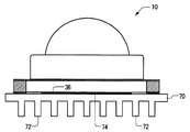
図4は、1つの外部ヒート・シンク70に結合されたダイ・パッケージ10を図示する。図4を参照するに、熱接点パッド36は、エポキシ、半田、または任意の他の熱伝導接着剤、導電接着剤、または熱電導接着剤74を使って外部ヒート・シンク70に取り付け可能である。外部ヒート・シンク70は、1つのプリント回路ボード(PCB)またはダイ・パッケージ10から熱を引出す他の構造にできる。外部ヒート・シンクは、様々な構成での複数の回路要素(示さず)または複数の熱拡散フィン72を含み得る。
FIG. 4 illustrates the
特定の代替的な構成を有する本発明の1つの実施形態が図5から6Dに示される。この第2の実施例の複数の部分は、図1Aから4の中に示す第1実施形態の複数の対応部分に類似している。便宜上、第1実施形態の複数部分に類似の図5から6D中に図示される第2の複数部分は、同じ参照番号を与えられている。相似ではあるが変更された部分には、”a”を伴った同じ参照番号が付けられ、異なる部分には異なる参照番号が割当られている。 One embodiment of the present invention having certain alternative configurations is shown in FIGS. 5-6D. The parts of this second example are similar to the corresponding parts of the first embodiment shown in FIGS. For convenience, the second plurality of parts illustrated in FIGS. 5 to 6D that are similar to the parts of the first embodiment are given the same reference numerals. Similar but changed parts are given the same reference number with "a" and different parts are assigned different reference numbers.
図5は、本発明の他の複数の実施形態による1つのLEDダイ・パッケージ10aの1つの組立分解透視図である。図5を参照するに、本発明の発光ダイ・パッケージ10aは、1つの底部ヒート・シンク(基板)20a、1つの上部ヒート・シンク(反射板)40a、および1つのレンズ50を含む。
FIG. 5 is an exploded perspective view of one
図6A、6B、6Cおよび6Dは、それぞれ、図5の基板20aの1つの平面図、1つの側面図、1つの正面図、および1つの底面図を提供する。図5から6Dを参照するに、説明用の実施形態において、基板20aは、1つの第1トレース22a、および四つの第2トレース24aを含む。これらのトレース22aおよび24aは、図2Aのトレース22および24とは異なる構成になっている。基板20aは、反射板40aを基板20aに機械的に係合する反射板40aの複数の脚35の受入のための複数のラッチ・スペース33を画定する複数のフランジ31を含む。
6A, 6B, 6C and 6D provide one top view, one side view, one front view, and one bottom view, respectively, of the
前述から明らかなことは、本発明は、新規なものであり、現在の技法を凌ぐ複数の利点を提供することである。本発明の具体的な実施形態を上に述べ、図示したが、本発明はその説明と図示の複数の部分の具体的な形状または配置に限定されるものではない。例えば、異なる複数の構成、複数の寸法、または複数の材料を本発明の実施に使用可能である。
本発明は、添付の特許請求の範囲によって制限される。次において、複数の請求項は、米国特許法112条に定められた”手段又は工程(means or step for)”の利益を得るために作成された複数の請求項は、”ための手段(means for)”なる句によって特定される。
It will be apparent from the foregoing that the present invention is novel and provides a number of advantages over current techniques. Although specific embodiments of the present invention have been described and illustrated above, the present invention is not limited to the specific shapes or arrangements of the parts described and illustrated. For example, different configurations, dimensions, or materials can be used in the practice of the invention.
The present invention is limited by the appended claims. In the following, a plurality of claims shall be defined as a “means or step for” benefit as set forth in 35 USC 112. for) ”.
Claims (40)
1つの取り付けパッドにおいて1つの発光ダイオード・アセンブリに接続される複数のトレースを有する1つの基板と、
前記基板に結合され、前記取り付けパッドを略囲む1つの反射板と、
前記取り付けパッドを略被うレンズと
を備える、発光ダイ・パッケージ。 A light emitting die package,
One substrate having a plurality of traces connected to one light emitting diode assembly at one mounting pad;
One reflector coupled to the substrate and substantially surrounding the mounting pad;
A light emitting die package comprising a lens that substantially covers the mounting pad.
1つの上面上に複数のトレースを有する1つの底部ヒート・シンクと、
前記底部ヒート・シンクの上面上に取り付けた1つの半導体チップであって、前記底部ヒート・シンクのトレースに電気的に接続される半導体チップと、
前記底部ヒート・シンクに機械的に結合された1つの上部ヒート・シンクと
を備える、半導体ダイ・パッケージ。 A semiconductor die package,
A bottom heat sink having a plurality of traces on a top surface;
A semiconductor chip mounted on the top surface of the bottom heat sink, the semiconductor chip being electrically connected to the bottom heat sink trace;
A semiconductor die package comprising a top heat sink mechanically coupled to the bottom heat sink.
Applications Claiming Priority (4)
| Application Number | Priority Date | Filing Date | Title |
|---|---|---|---|
| US40825402P | 2002-09-04 | 2002-09-04 | |
| US60/408,254 | 2002-09-04 | ||
| US10/446,532 US7264378B2 (en) | 2002-09-04 | 2003-05-27 | Power surface mount light emitting die package |
| US10/446,532 | 2003-05-27 |
Related Parent Applications (1)
| Application Number | Title | Priority Date | Filing Date |
|---|---|---|---|
| JP2004534428A Division JP4731906B2 (en) | 2002-09-04 | 2003-09-02 | Power surface mounted light emitting die package |
Publications (2)
| Publication Number | Publication Date |
|---|---|
| JP2011129948A true JP2011129948A (en) | 2011-06-30 |
| JP5520242B2 JP5520242B2 (en) | 2014-06-11 |
Family
ID=31981582
Family Applications (8)
| Application Number | Title | Priority Date | Filing Date |
|---|---|---|---|
| JP2004534428A Expired - Lifetime JP4731906B2 (en) | 2002-09-04 | 2003-09-02 | Power surface mounted light emitting die package |
| JP2011032601A Expired - Lifetime JP5520242B2 (en) | 2002-09-04 | 2011-02-17 | Power surface mounted light emitting die package |
| JP2011032598A Expired - Lifetime JP5746877B2 (en) | 2002-09-04 | 2011-02-17 | Power surface mounted light emitting die package |
| JP2011032600A Expired - Lifetime JP5629601B2 (en) | 2002-09-04 | 2011-02-17 | Power surface mounted light emitting die package |
| JP2011032603A Pending JP2011139087A (en) | 2002-09-04 | 2011-02-17 | Power surface mount light emitting die package |
| JP2011032602A Pending JP2011129949A (en) | 2002-09-04 | 2011-02-17 | Power surface mount light emitting die package |
| JP2011032604A Expired - Lifetime JP5520243B2 (en) | 2002-09-04 | 2011-02-17 | Power surface mounted light emitting die package |
| JP2011032599A Expired - Lifetime JP5520241B2 (en) | 2002-09-04 | 2011-02-17 | Power surface mounted light emitting die package |
Family Applications Before (1)
| Application Number | Title | Priority Date | Filing Date |
|---|---|---|---|
| JP2004534428A Expired - Lifetime JP4731906B2 (en) | 2002-09-04 | 2003-09-02 | Power surface mounted light emitting die package |
Family Applications After (6)
| Application Number | Title | Priority Date | Filing Date |
|---|---|---|---|
| JP2011032598A Expired - Lifetime JP5746877B2 (en) | 2002-09-04 | 2011-02-17 | Power surface mounted light emitting die package |
| JP2011032600A Expired - Lifetime JP5629601B2 (en) | 2002-09-04 | 2011-02-17 | Power surface mounted light emitting die package |
| JP2011032603A Pending JP2011139087A (en) | 2002-09-04 | 2011-02-17 | Power surface mount light emitting die package |
| JP2011032602A Pending JP2011129949A (en) | 2002-09-04 | 2011-02-17 | Power surface mount light emitting die package |
| JP2011032604A Expired - Lifetime JP5520243B2 (en) | 2002-09-04 | 2011-02-17 | Power surface mounted light emitting die package |
| JP2011032599A Expired - Lifetime JP5520241B2 (en) | 2002-09-04 | 2011-02-17 | Power surface mounted light emitting die package |
Country Status (11)
| Country | Link |
|---|---|
| US (1) | US7264378B2 (en) |
| EP (2) | EP1953825B1 (en) |
| JP (8) | JP4731906B2 (en) |
| KR (5) | KR101088928B1 (en) |
| CN (1) | CN100414698C (en) |
| AT (1) | ATE400896T1 (en) |
| AU (1) | AU2003276860A1 (en) |
| CA (1) | CA2496937A1 (en) |
| DE (1) | DE60322074D1 (en) |
| TW (1) | TWI331380B (en) |
| WO (1) | WO2004023522A2 (en) |
Families Citing this family (266)
| Publication number | Priority date | Publication date | Assignee | Title |
|---|---|---|---|---|
| WO2004021461A2 (en) | 2002-08-30 | 2004-03-11 | Gelcore Llc | Phosphor-coated led with improved efficiency |
| US10340424B2 (en) | 2002-08-30 | 2019-07-02 | GE Lighting Solutions, LLC | Light emitting diode component |
| US7800121B2 (en) | 2002-08-30 | 2010-09-21 | Lumination Llc | Light emitting diode component |
| US7775685B2 (en) * | 2003-05-27 | 2010-08-17 | Cree, Inc. | Power surface mount light emitting die package |
| US7264378B2 (en) * | 2002-09-04 | 2007-09-04 | Cree, Inc. | Power surface mount light emitting die package |
| US7244965B2 (en) * | 2002-09-04 | 2007-07-17 | Cree Inc, | Power surface mount light emitting die package |
| US20050023260A1 (en) * | 2003-01-10 | 2005-02-03 | Shinya Takyu | Semiconductor wafer dividing apparatus and semiconductor device manufacturing method |
| EP1629537B1 (en) * | 2003-05-30 | 2014-07-30 | OSRAM Opto Semiconductors GmbH | Light-emitting diode |
| EP1484802B1 (en) * | 2003-06-06 | 2018-06-13 | Stanley Electric Co., Ltd. | Optical semiconductor device |
| JP2005073227A (en) * | 2003-08-04 | 2005-03-17 | Sharp Corp | Image pickup device |
| US20050104072A1 (en) | 2003-08-14 | 2005-05-19 | Slater David B.Jr. | Localized annealing of metal-silicon carbide ohmic contacts and devices so formed |
| US7183587B2 (en) * | 2003-09-09 | 2007-02-27 | Cree, Inc. | Solid metal block mounting substrates for semiconductor light emitting devices |
| US7915085B2 (en) | 2003-09-18 | 2011-03-29 | Cree, Inc. | Molded chip fabrication method |
| US7518158B2 (en) * | 2003-12-09 | 2009-04-14 | Cree, Inc. | Semiconductor light emitting devices and submounts |
| US7397067B2 (en) * | 2003-12-31 | 2008-07-08 | Intel Corporation | Microdisplay packaging system |
| US10499465B2 (en) | 2004-02-25 | 2019-12-03 | Lynk Labs, Inc. | High frequency multi-voltage and multi-brightness LED lighting devices and systems and methods of using same |
| US10575376B2 (en) | 2004-02-25 | 2020-02-25 | Lynk Labs, Inc. | AC light emitting diode and AC LED drive methods and apparatus |
| WO2011143510A1 (en) | 2010-05-12 | 2011-11-17 | Lynk Labs, Inc. | Led lighting system |
| DE102004014207A1 (en) * | 2004-03-23 | 2005-10-13 | Osram Opto Semiconductors Gmbh | Optoelectronic component with a multi-part housing body |
| US7355284B2 (en) | 2004-03-29 | 2008-04-08 | Cree, Inc. | Semiconductor light emitting devices including flexible film having therein an optical element |
| US7326583B2 (en) | 2004-03-31 | 2008-02-05 | Cree, Inc. | Methods for packaging of a semiconductor light emitting device |
| JP4229447B2 (en) * | 2004-03-31 | 2009-02-25 | スタンレー電気株式会社 | Semiconductor light emitting device and manufacturing method |
| US7279346B2 (en) * | 2004-03-31 | 2007-10-09 | Cree, Inc. | Method for packaging a light emitting device by one dispense then cure step followed by another |
| US7517728B2 (en) * | 2004-03-31 | 2009-04-14 | Cree, Inc. | Semiconductor light emitting devices including a luminescent conversion element |
| US20050225222A1 (en) * | 2004-04-09 | 2005-10-13 | Joseph Mazzochette | Light emitting diode arrays with improved light extraction |
| KR100643582B1 (en) | 2004-04-26 | 2006-11-10 | 루미마이크로 주식회사 | Light Emitting Diode package |
| US7361938B2 (en) * | 2004-06-03 | 2008-04-22 | Philips Lumileds Lighting Company Llc | Luminescent ceramic for a light emitting device |
| US7280288B2 (en) * | 2004-06-04 | 2007-10-09 | Cree, Inc. | Composite optical lens with an integrated reflector |
| US7456499B2 (en) * | 2004-06-04 | 2008-11-25 | Cree, Inc. | Power light emitting die package with reflecting lens and the method of making the same |
| WO2006005062A2 (en) * | 2004-06-30 | 2006-01-12 | Cree, Inc. | Chip-scale methods for packaging light emitting devices and chip-scale packaged light emitting devices |
| KR100609734B1 (en) * | 2004-07-02 | 2006-08-08 | 럭스피아 주식회사 | Led package for use in back light of lcd and method of the same |
| US7252408B2 (en) * | 2004-07-19 | 2007-08-07 | Lamina Ceramics, Inc. | LED array package with internal feedback and control |
| US7118262B2 (en) * | 2004-07-23 | 2006-10-10 | Cree, Inc. | Reflective optical elements for semiconductor light emitting devices |
| US7201495B2 (en) * | 2004-08-03 | 2007-04-10 | Philips Lumileds Lighting Company, Llc | Semiconductor light emitting device package with cover with flexible portion |
| US7405093B2 (en) * | 2004-08-18 | 2008-07-29 | Cree, Inc. | Methods of assembly for a semiconductor light emitting device package |
| KR100604469B1 (en) * | 2004-08-25 | 2006-07-25 | 박병재 | light emitting device and package structure and method of manufacturing thereof |
| US7417220B2 (en) * | 2004-09-09 | 2008-08-26 | Toyoda Gosei Co., Ltd. | Solid state device and light-emitting element |
| EP1794808B1 (en) * | 2004-09-10 | 2017-08-09 | Seoul Semiconductor Co., Ltd. | Light emitting diode package having multiple molding resins |
| US7217583B2 (en) * | 2004-09-21 | 2007-05-15 | Cree, Inc. | Methods of coating semiconductor light emitting elements by evaporating solvent from a suspension |
| JP2006100633A (en) * | 2004-09-30 | 2006-04-13 | Toyoda Gosei Co Ltd | Led lighting device |
| CN101036238B (en) * | 2004-10-04 | 2014-01-08 | 株式会社东芝 | Light emitting device, lighting equipment or liquid crystal display device using such light emitting device |
| TWI405349B (en) * | 2004-10-07 | 2013-08-11 | Seoul Semiconductor Co Ltd | Side-luminescence lens and luminescent device suing the same |
| US20060097385A1 (en) * | 2004-10-25 | 2006-05-11 | Negley Gerald H | Solid metal block semiconductor light emitting device mounting substrates and packages including cavities and heat sinks, and methods of packaging same |
| DE102005028748A1 (en) * | 2004-10-25 | 2006-05-04 | Osram Opto Semiconductors Gmbh | Electromagnetic radiation emitting semiconductor device and device package |
| US8134292B2 (en) * | 2004-10-29 | 2012-03-13 | Ledengin, Inc. | Light emitting device with a thermal insulating and refractive index matching material |
| US8324641B2 (en) * | 2007-06-29 | 2012-12-04 | Ledengin, Inc. | Matrix material including an embedded dispersion of beads for a light-emitting device |
| US7329982B2 (en) * | 2004-10-29 | 2008-02-12 | 3M Innovative Properties Company | LED package with non-bonded optical element |
| US7772609B2 (en) * | 2004-10-29 | 2010-08-10 | Ledengin, Inc. (Cayman) | LED package with structure and materials for high heat dissipation |
| US7670872B2 (en) * | 2004-10-29 | 2010-03-02 | LED Engin, Inc. (Cayman) | Method of manufacturing ceramic LED packages |
| US9929326B2 (en) | 2004-10-29 | 2018-03-27 | Ledengin, Inc. | LED package having mushroom-shaped lens with volume diffuser |
| US7473933B2 (en) * | 2004-10-29 | 2009-01-06 | Ledengin, Inc. (Cayman) | High power LED package with universal bonding pads and interconnect arrangement |
| US8816369B2 (en) | 2004-10-29 | 2014-08-26 | Led Engin, Inc. | LED packages with mushroom shaped lenses and methods of manufacturing LED light-emitting devices |
| US20060091414A1 (en) * | 2004-10-29 | 2006-05-04 | Ouderkirk Andrew J | LED package with front surface heat extractor |
| US20060124953A1 (en) * | 2004-12-14 | 2006-06-15 | Negley Gerald H | Semiconductor light emitting device mounting substrates and packages including cavities and cover plates, and methods of packaging same |
| WO2006065007A1 (en) * | 2004-12-16 | 2006-06-22 | Seoul Semiconductor Co., Ltd. | Leadframe having a heat sink supporting ring, fabricating method of a light emitting diodepackage using the same and light emitting diodepackage fabbricated by the method |
| KR100580753B1 (en) * | 2004-12-17 | 2006-05-15 | 엘지이노텍 주식회사 | Light emitting device package |
| KR100646093B1 (en) * | 2004-12-17 | 2006-11-15 | 엘지이노텍 주식회사 | Light emitting device package |
| US7322732B2 (en) * | 2004-12-23 | 2008-01-29 | Cree, Inc. | Light emitting diode arrays for direct backlighting of liquid crystal displays |
| US8288942B2 (en) * | 2004-12-28 | 2012-10-16 | Cree, Inc. | High efficacy white LED |
| TWI248218B (en) * | 2004-12-31 | 2006-01-21 | Ind Tech Res Inst | Light-emitting diode package structure and fabrication method thereof |
| US7821023B2 (en) | 2005-01-10 | 2010-10-26 | Cree, Inc. | Solid state lighting component |
| US9070850B2 (en) | 2007-10-31 | 2015-06-30 | Cree, Inc. | Light emitting diode package and method for fabricating same |
| US9793247B2 (en) | 2005-01-10 | 2017-10-17 | Cree, Inc. | Solid state lighting component |
| US7304694B2 (en) * | 2005-01-12 | 2007-12-04 | Cree, Inc. | Solid colloidal dispersions for backlighting of liquid crystal displays |
| US7777247B2 (en) * | 2005-01-14 | 2010-08-17 | Cree, Inc. | Semiconductor light emitting device mounting substrates including a conductive lead extending therein |
| US20060171152A1 (en) * | 2005-01-20 | 2006-08-03 | Toyoda Gosei Co., Ltd. | Light emitting device and method of making the same |
| US7939842B2 (en) * | 2005-01-27 | 2011-05-10 | Cree, Inc. | Light emitting device packages, light emitting diode (LED) packages and related methods |
| US20080296589A1 (en) * | 2005-03-24 | 2008-12-04 | Ingo Speier | Solid-State Lighting Device Package |
| CA2614803C (en) * | 2005-04-05 | 2015-08-25 | Tir Technology Lp | Electronic device package with an integrated evaporator |
| CN100420019C (en) * | 2005-04-20 | 2008-09-17 | 王锐勋 | Packaging method for colony light-emitting diode chips and devices thereof |
| US7425083B2 (en) * | 2005-05-02 | 2008-09-16 | Samsung Electro-Mechanics Co., Ltd. | Light emitting device package |
| KR100649641B1 (en) * | 2005-05-31 | 2006-11-27 | 삼성전기주식회사 | Led package |
| KR100616684B1 (en) * | 2005-06-03 | 2006-08-28 | 삼성전기주식회사 | High power led package and fabrication method thereof |
| US8669572B2 (en) * | 2005-06-10 | 2014-03-11 | Cree, Inc. | Power lamp package |
| US7980743B2 (en) | 2005-06-14 | 2011-07-19 | Cree, Inc. | LED backlighting for displays |
| JP2006352047A (en) * | 2005-06-20 | 2006-12-28 | Rohm Co Ltd | Optical semiconductor device |
| US20060292747A1 (en) * | 2005-06-27 | 2006-12-28 | Loh Ban P | Top-surface-mount power light emitter with integral heat sink |
| TWI287300B (en) * | 2005-06-30 | 2007-09-21 | Lite On Technology Corp | Semiconductor package structure |
| TWI422044B (en) * | 2005-06-30 | 2014-01-01 | Cree Inc | Chip-scale methods for packaging light emitting devices and chip-scale packaged light emitting devices |
| KR100632003B1 (en) * | 2005-08-08 | 2006-10-09 | 삼성전기주식회사 | Led package having recess in heat transfer part |
| JP2009513021A (en) * | 2005-10-24 | 2009-03-26 | スリーエム イノベイティブ プロパティズ カンパニー | Method of manufacturing light emitting device having molded encapsulant |
| KR101013308B1 (en) * | 2005-11-24 | 2011-02-09 | 요이치 마츠오카 | Electronic component mounting board and method for manufacturing such board |
| KR100780176B1 (en) | 2005-11-25 | 2007-11-27 | 삼성전기주식회사 | Side-view light emitting diode package |
| US8465175B2 (en) * | 2005-11-29 | 2013-06-18 | GE Lighting Solutions, LLC | LED lighting assemblies with thermal overmolding |
| CN101460779A (en) * | 2005-12-21 | 2009-06-17 | 科锐Led照明技术公司 | Lighting device |
| US7614759B2 (en) | 2005-12-22 | 2009-11-10 | Cree Led Lighting Solutions, Inc. | Lighting device |
| KR100648628B1 (en) * | 2005-12-29 | 2006-11-24 | 서울반도체 주식회사 | Light emitting diode |
| US8441179B2 (en) | 2006-01-20 | 2013-05-14 | Cree, Inc. | Lighting devices having remote lumiphors that are excited by lumiphor-converted semiconductor excitation sources |
| US8264138B2 (en) * | 2006-01-20 | 2012-09-11 | Cree, Inc. | Shifting spectral content in solid state light emitters by spatially separating lumiphor films |
| WO2007088584A1 (en) * | 2006-01-31 | 2007-08-09 | Fujitsu Limited | Optical module and method for manufacturing same |
| JP4828248B2 (en) * | 2006-02-16 | 2011-11-30 | 新光電気工業株式会社 | Light emitting device and manufacturing method thereof |
| JP2009231847A (en) * | 2006-03-02 | 2009-10-08 | Tokuyama Corp | Support for semiconductor device, and manufacturing method therefor |
| US7808004B2 (en) * | 2006-03-17 | 2010-10-05 | Edison Opto Corporation | Light emitting diode package structure and method of manufacturing the same |
| US7675145B2 (en) * | 2006-03-28 | 2010-03-09 | Cree Hong Kong Limited | Apparatus, system and method for use in mounting electronic elements |
| US8969908B2 (en) | 2006-04-04 | 2015-03-03 | Cree, Inc. | Uniform emission LED package |
| US7863639B2 (en) * | 2006-04-12 | 2011-01-04 | Semileds Optoelectronics Co. Ltd. | Light-emitting diode lamp with low thermal resistance |
| US8373195B2 (en) | 2006-04-12 | 2013-02-12 | SemiLEDs Optoelectronics Co., Ltd. | Light-emitting diode lamp with low thermal resistance |
| US8748915B2 (en) | 2006-04-24 | 2014-06-10 | Cree Hong Kong Limited | Emitter package with angled or vertical LED |
| US11210971B2 (en) | 2009-07-06 | 2021-12-28 | Cree Huizhou Solid State Lighting Company Limited | Light emitting diode display with tilted peak emission pattern |
| US7635915B2 (en) | 2006-04-26 | 2009-12-22 | Cree Hong Kong Limited | Apparatus and method for use in mounting electronic elements |
| US7655957B2 (en) * | 2006-04-27 | 2010-02-02 | Cree, Inc. | Submounts for semiconductor light emitting device packages and semiconductor light emitting device packages including the same |
| US7525126B2 (en) | 2006-05-02 | 2009-04-28 | 3M Innovative Properties Company | LED package with converging optical element |
| US7953293B2 (en) * | 2006-05-02 | 2011-05-31 | Ati Technologies Ulc | Field sequence detector, method and video device |
| US20070257270A1 (en) * | 2006-05-02 | 2007-11-08 | 3M Innovative Properties Company | Led package with wedge-shaped optical element |
| US20070257271A1 (en) * | 2006-05-02 | 2007-11-08 | 3M Innovative Properties Company | Led package with encapsulated converging optical element |
| US7390117B2 (en) * | 2006-05-02 | 2008-06-24 | 3M Innovative Properties Company | LED package with compound converging optical element |
| US7655486B2 (en) * | 2006-05-17 | 2010-02-02 | 3M Innovative Properties Company | Method of making light emitting device with multilayer silicon-containing encapsulant |
| US20070269586A1 (en) * | 2006-05-17 | 2007-11-22 | 3M Innovative Properties Company | Method of making light emitting device with silicon-containing composition |
| US8033692B2 (en) * | 2006-05-23 | 2011-10-11 | Cree, Inc. | Lighting device |
| JP2009538531A (en) * | 2006-05-23 | 2009-11-05 | クリー エル イー ディー ライティング ソリューションズ インコーポレイテッド | LIGHTING DEVICE AND MANUFACTURING METHOD |
| US7703945B2 (en) * | 2006-06-27 | 2010-04-27 | Cree, Inc. | Efficient emitting LED package and method for efficiently emitting light |
| US7906794B2 (en) * | 2006-07-05 | 2011-03-15 | Koninklijke Philips Electronics N.V. | Light emitting device package with frame and optically transmissive element |
| US8044418B2 (en) * | 2006-07-13 | 2011-10-25 | Cree, Inc. | Leadframe-based packages for solid state light emitting devices |
| US7960819B2 (en) * | 2006-07-13 | 2011-06-14 | Cree, Inc. | Leadframe-based packages for solid state emitting devices |
| US20080012034A1 (en) * | 2006-07-17 | 2008-01-17 | 3M Innovative Properties Company | Led package with converging extractor |
| US8735920B2 (en) | 2006-07-31 | 2014-05-27 | Cree, Inc. | Light emitting diode package with optical element |
| US7943952B2 (en) | 2006-07-31 | 2011-05-17 | Cree, Inc. | Method of uniform phosphor chip coating and LED package fabricated using method |
| TWI418054B (en) * | 2006-08-08 | 2013-12-01 | Lg Electronics Inc | Light emitting device package and method for manufacturing the same |
| US8367945B2 (en) | 2006-08-16 | 2013-02-05 | Cree Huizhou Opto Limited | Apparatus, system and method for use in mounting electronic elements |
| US7763478B2 (en) * | 2006-08-21 | 2010-07-27 | Cree, Inc. | Methods of forming semiconductor light emitting device packages by liquid injection molding |
| KR101258227B1 (en) | 2006-08-29 | 2013-04-25 | 서울반도체 주식회사 | Light emitting device |
| US7842960B2 (en) | 2006-09-06 | 2010-11-30 | Lumination Llc | Light emitting packages and methods of making same |
| TW200814362A (en) * | 2006-09-13 | 2008-03-16 | Bright Led Electronics Corp | Light-emitting diode device with high heat dissipation property |
| EP1903361B1 (en) * | 2006-09-22 | 2020-04-01 | Nippon Electric Glass Co., Ltd. | Optical component and light emitting device using the same |
| KR100757826B1 (en) * | 2006-09-29 | 2007-09-11 | 서울반도체 주식회사 | Side-view light emitting diode package |
| DE102006047233A1 (en) * | 2006-10-04 | 2008-04-10 | Osram Opto Semiconductors Gmbh | Optical element for a light-emitting diode, light-emitting diode, LED arrangement and method for producing an LED arrangement |
| KR101484488B1 (en) * | 2006-10-31 | 2015-01-20 | 코닌클리케 필립스 엔.브이. | Lighting device package |
| US7808013B2 (en) * | 2006-10-31 | 2010-10-05 | Cree, Inc. | Integrated heat spreaders for light emitting devices (LEDs) and related assemblies |
| US10295147B2 (en) | 2006-11-09 | 2019-05-21 | Cree, Inc. | LED array and method for fabricating same |
| WO2008073400A1 (en) | 2006-12-11 | 2008-06-19 | The Regents Of The University Of California | Transparent light emitting diodes |
| WO2008078237A2 (en) * | 2006-12-21 | 2008-07-03 | Koninklijke Philips Electronics N.V. | Carrier and optical semiconductor device based on such a carrier |
| DE102006062066A1 (en) * | 2006-12-29 | 2008-07-03 | Osram Opto Semiconductors Gmbh | Lens arrangement for light emitting diode display device, has lens with lens surface and optical axis, which penetrates lens surface of lens |
| US8232564B2 (en) | 2007-01-22 | 2012-07-31 | Cree, Inc. | Wafer level phosphor coating technique for warm light emitting diodes |
| US9024349B2 (en) | 2007-01-22 | 2015-05-05 | Cree, Inc. | Wafer level phosphor coating method and devices fabricated utilizing method |
| US9159888B2 (en) | 2007-01-22 | 2015-10-13 | Cree, Inc. | Wafer level phosphor coating method and devices fabricated utilizing method |
| DE102007006349A1 (en) * | 2007-01-25 | 2008-07-31 | Osram Opto Semiconductors Gmbh | Arrangement for generating mixed light and method for producing such an arrangement |
| TWI367573B (en) * | 2007-01-31 | 2012-07-01 | Young Lighting Technology Inc | Light emitting diode package and manufacturing method thereof |
| WO2008092271A1 (en) * | 2007-02-01 | 2008-08-07 | Aimrail Corp. | Multiple axes adjustable lighting system with movable thermally conductive carriage |
| US7709853B2 (en) * | 2007-02-12 | 2010-05-04 | Cree, Inc. | Packaged semiconductor light emitting devices having multiple optical elements |
| US9061450B2 (en) | 2007-02-12 | 2015-06-23 | Cree, Inc. | Methods of forming packaged semiconductor light emitting devices having front contacts by compression molding |
| US9711703B2 (en) * | 2007-02-12 | 2017-07-18 | Cree Huizhou Opto Limited | Apparatus, system and method for use in mounting electronic elements |
| TW200838354A (en) * | 2007-03-03 | 2008-09-16 | Ind Tech Res Inst | Resistance balance circuit |
| TWI323384B (en) * | 2007-04-09 | 2010-04-11 | Coretronic Corp | Light valve device |
| US7964888B2 (en) | 2007-04-18 | 2011-06-21 | Cree, Inc. | Semiconductor light emitting device packages and methods |
| US7910944B2 (en) * | 2007-05-04 | 2011-03-22 | Cree, Inc. | Side mountable semiconductor light emitting device packages and panels |
| US8436371B2 (en) * | 2007-05-24 | 2013-05-07 | Cree, Inc. | Microscale optoelectronic device packages |
| US7992294B2 (en) * | 2007-05-25 | 2011-08-09 | Molex Incorporated | Method of manufacturing an interconnect device which forms a heat sink and electrical connections between a heat generating device and a power source |
| JP5233170B2 (en) * | 2007-05-31 | 2013-07-10 | 日亜化学工業株式会社 | LIGHT EMITTING DEVICE, RESIN MOLDED BODY FORMING LIGHT EMITTING DEVICE, AND METHOD FOR PRODUCING THEM |
| US20090008662A1 (en) * | 2007-07-05 | 2009-01-08 | Ian Ashdown | Lighting device package |
| US10505083B2 (en) | 2007-07-11 | 2019-12-10 | Cree, Inc. | Coating method utilizing phosphor containment structure and devices fabricated using same |
| EP2017897A1 (en) | 2007-07-16 | 2009-01-21 | ILED Photoelectronics Inc. | Package structure for a high-luminance light source |
| CN101743488B (en) | 2007-07-17 | 2014-02-26 | 科锐公司 | Optical elements with internal optical features and methods of fabricating same |
| CN101369619B (en) * | 2007-08-14 | 2011-01-05 | 富士迈半导体精密工业(上海)有限公司 | Surface labeling type LED component and LED back light module unit |
| TWI353096B (en) * | 2007-08-20 | 2011-11-21 | Young Optics Inc | Optoelectronic semiconductor package and method fo |
| US7968899B2 (en) * | 2007-08-27 | 2011-06-28 | Avago Technologies Ecbu Ip (Singapore) Pte. Ltd. | LED light source having improved resistance to thermal cycling |
| EP2193554B1 (en) * | 2007-09-20 | 2015-12-02 | Philips Intellectual Property & Standards GmbH | Light emitting diode package |
| US20090091934A1 (en) * | 2007-10-05 | 2009-04-09 | Cosmo Electronics Corporation | High power LED module |
| US11317495B2 (en) | 2007-10-06 | 2022-04-26 | Lynk Labs, Inc. | LED circuits and assemblies |
| US11297705B2 (en) | 2007-10-06 | 2022-04-05 | Lynk Labs, Inc. | Multi-voltage and multi-brightness LED lighting devices and methods of using same |
| CN101226976B (en) * | 2007-10-09 | 2012-01-04 | 番禺得意精密电子工业有限公司 | LED device and locating structure thereof |
| US8866169B2 (en) | 2007-10-31 | 2014-10-21 | Cree, Inc. | LED package with increased feature sizes |
| USD615504S1 (en) | 2007-10-31 | 2010-05-11 | Cree, Inc. | Emitter package |
| US10256385B2 (en) | 2007-10-31 | 2019-04-09 | Cree, Inc. | Light emitting die (LED) packages and related methods |
| US9634191B2 (en) * | 2007-11-14 | 2017-04-25 | Cree, Inc. | Wire bond free wafer level LED |
| US8536584B2 (en) * | 2007-11-14 | 2013-09-17 | Cree, Inc. | High voltage wire bond free LEDS |
| US8575633B2 (en) * | 2008-12-08 | 2013-11-05 | Cree, Inc. | Light emitting diode with improved light extraction |
| USD633631S1 (en) | 2007-12-14 | 2011-03-01 | Cree Hong Kong Limited | Light source of light emitting diode |
| US9041285B2 (en) | 2007-12-14 | 2015-05-26 | Cree, Inc. | Phosphor distribution in LED lamps using centrifugal force |
| US8167674B2 (en) | 2007-12-14 | 2012-05-01 | Cree, Inc. | Phosphor distribution in LED lamps using centrifugal force |
| TW200928203A (en) * | 2007-12-24 | 2009-07-01 | Guei-Fang Chen | LED illuminating device capable of quickly dissipating heat and its manufacturing method |
| USD634863S1 (en) | 2008-01-10 | 2011-03-22 | Cree Hong Kong Limited | Light source of light emitting diode |
| US8637883B2 (en) | 2008-03-19 | 2014-01-28 | Cree, Inc. | Low index spacer layer in LED devices |
| DE202008005987U1 (en) * | 2008-04-30 | 2009-09-03 | Ledon Lighting Jennersdorf Gmbh | LED module with dome-shaped color conversion layer |
| US8049230B2 (en) | 2008-05-16 | 2011-11-01 | Cree Huizhou Opto Limited | Apparatus and system for miniature surface mount devices |
| US8240875B2 (en) | 2008-06-25 | 2012-08-14 | Cree, Inc. | Solid state linear array modules for general illumination |
| CN101614326A (en) * | 2008-06-27 | 2009-12-30 | 富准精密工业(深圳)有限公司 | Light emitting diode |
| CN101577301B (en) * | 2008-09-05 | 2011-12-21 | 佛山市国星光电股份有限公司 | Package method for white light LED and LED device manufactured by package method for white light LED |
| DE102008049535A1 (en) * | 2008-09-29 | 2010-04-08 | Osram Opto Semiconductors Gmbh | LED module and manufacturing process |
| US8075165B2 (en) | 2008-10-14 | 2011-12-13 | Ledengin, Inc. | Total internal reflection lens and mechanical retention and locating device |
| US9425172B2 (en) | 2008-10-24 | 2016-08-23 | Cree, Inc. | Light emitter array |
| US8791471B2 (en) | 2008-11-07 | 2014-07-29 | Cree Hong Kong Limited | Multi-chip light emitting diode modules |
| US20100117106A1 (en) * | 2008-11-07 | 2010-05-13 | Ledengin, Inc. | Led with light-conversion layer |
| KR101007131B1 (en) * | 2008-11-25 | 2011-01-10 | 엘지이노텍 주식회사 | Light emitting device package |
| US8507300B2 (en) * | 2008-12-24 | 2013-08-13 | Ledengin, Inc. | Light-emitting diode with light-conversion layer |
| TWI426206B (en) * | 2008-12-25 | 2014-02-11 | Au Optronics Corp | Light emitting diode apparatus |
| US8368112B2 (en) * | 2009-01-14 | 2013-02-05 | Cree Huizhou Opto Limited | Aligned multiple emitter package |
| US20100237364A1 (en) * | 2009-03-19 | 2010-09-23 | Christy Alexander C | Thermal Energy Dissipating and Light Emitting Diode Mounting Arrangement |
| US8598793B2 (en) | 2011-05-12 | 2013-12-03 | Ledengin, Inc. | Tuning of emitter with multiple LEDs to a single color bin |
| US8384097B2 (en) | 2009-04-08 | 2013-02-26 | Ledengin, Inc. | Package for multiple light emitting diodes |
| US7985000B2 (en) * | 2009-04-08 | 2011-07-26 | Ledengin, Inc. | Lighting apparatus having multiple light-emitting diodes with individual light-conversion layers |
| US8415692B2 (en) | 2009-07-06 | 2013-04-09 | Cree, Inc. | LED packages with scattering particle regions |
| US8598809B2 (en) | 2009-08-19 | 2013-12-03 | Cree, Inc. | White light color changing solid state lighting and methods |
| US9385285B2 (en) | 2009-09-17 | 2016-07-05 | Koninklijke Philips N.V. | LED module with high index lens |
| TWI416771B (en) * | 2009-10-01 | 2013-11-21 | Everlight Electronics Co Ltd | Light emitting diode |
| US8593040B2 (en) | 2009-10-02 | 2013-11-26 | Ge Lighting Solutions Llc | LED lamp with surface area enhancing fins |
| KR101163850B1 (en) * | 2009-11-23 | 2012-07-09 | 엘지이노텍 주식회사 | Light emitting device package |
| US8466611B2 (en) | 2009-12-14 | 2013-06-18 | Cree, Inc. | Lighting device with shaped remote phosphor |
| US8303141B2 (en) * | 2009-12-17 | 2012-11-06 | Ledengin, Inc. | Total internal reflection lens with integrated lamp cover |
| US9345095B2 (en) | 2010-04-08 | 2016-05-17 | Ledengin, Inc. | Tunable multi-LED emitter module |
| US9080729B2 (en) | 2010-04-08 | 2015-07-14 | Ledengin, Inc. | Multiple-LED emitter for A-19 lamps |
| US8858022B2 (en) | 2011-05-05 | 2014-10-14 | Ledengin, Inc. | Spot TIR lens system for small high-power emitter |
| ITMI20100108U1 (en) * | 2010-04-08 | 2011-10-09 | Marco Gaeta | MINIATURIZED LED LAMP OF REPLACEABLE POWER |
| US9012938B2 (en) | 2010-04-09 | 2015-04-21 | Cree, Inc. | High reflective substrate of light emitting devices with improved light output |
| KR101298406B1 (en) * | 2010-05-17 | 2013-08-20 | 엘지이노텍 주식회사 | Light Emitting Device |
| CN102270725A (en) * | 2010-06-01 | 2011-12-07 | 展晶科技(深圳)有限公司 | Light emitting diode packaging structure |
| US10546846B2 (en) | 2010-07-23 | 2020-01-28 | Cree, Inc. | Light transmission control for masking appearance of solid state light sources |
| US8455882B2 (en) | 2010-10-15 | 2013-06-04 | Cree, Inc. | High efficiency LEDs |
| US8232574B2 (en) | 2010-10-28 | 2012-07-31 | Avago Technologies Ecbu Ip (Singapore) Pte. Ltd. | Light emitting package with a mechanical latch |
| US9029991B2 (en) * | 2010-11-16 | 2015-05-12 | Conexant Systems, Inc. | Semiconductor packages with reduced solder voiding |
| US9273914B2 (en) * | 2010-11-29 | 2016-03-01 | Kyocera Corporation | Electronic component mounting package and electronic apparatus using the same |
| US8772817B2 (en) | 2010-12-22 | 2014-07-08 | Cree, Inc. | Electronic device submounts including substrates with thermally conductive vias |
| KR101766299B1 (en) * | 2011-01-20 | 2017-08-08 | 삼성전자 주식회사 | Light emitting device package and method of manufacturing the light emitting device package |
| US9166126B2 (en) | 2011-01-31 | 2015-10-20 | Cree, Inc. | Conformally coated light emitting devices and methods for providing the same |
| EP2482333A1 (en) | 2011-01-31 | 2012-08-01 | AZURSPACE Solar Power GmbH | Solar cell receiver |
| CN102644855B (en) * | 2011-02-18 | 2015-01-07 | 海洋王照明科技股份有限公司 | White-light LED (Light-Emitting Diode) light source |
| TWI517452B (en) * | 2011-03-02 | 2016-01-11 | 建準電機工業股份有限公司 | Packaging structure for plural bare chip |
| US8405181B2 (en) * | 2011-03-16 | 2013-03-26 | Intellectual Discovery Co., Ltd. | High brightness and high contrast plastic leaded chip carrier LED |
| TWI508333B (en) * | 2011-05-09 | 2015-11-11 | Lextar Electronics Corp | Led frame structure and led unit having the same |
| US8513900B2 (en) | 2011-05-12 | 2013-08-20 | Ledengin, Inc. | Apparatus for tuning of emitter with multiple LEDs to a single color bin |
| KR101212654B1 (en) * | 2011-05-20 | 2012-12-14 | (주)라이타이저코리아 | Package for light emitting diode and method for manufacturing thereof |
| CN102798103B (en) * | 2011-05-24 | 2016-06-01 | 奥斯兰姆有限公司 | Module radiator for LED |
| TW201313455A (en) * | 2011-09-28 | 2013-04-01 | Ichia Tech Inc | Method for bonding plastic mold member onto metal housing |
| US8564004B2 (en) | 2011-11-29 | 2013-10-22 | Cree, Inc. | Complex primary optics with intermediate elements |
| US9247597B2 (en) | 2011-12-02 | 2016-01-26 | Lynk Labs, Inc. | Color temperature controlled and low THD LED lighting devices and systems and methods of driving the same |
| US11032884B2 (en) | 2012-03-02 | 2021-06-08 | Ledengin, Inc. | Method for making tunable multi-led emitter module |
| US9897284B2 (en) | 2012-03-28 | 2018-02-20 | Ledengin, Inc. | LED-based MR16 replacement lamp |
| US9500355B2 (en) | 2012-05-04 | 2016-11-22 | GE Lighting Solutions, LLC | Lamp with light emitting elements surrounding active cooling device |
| PT2693495T (en) | 2012-07-31 | 2020-11-17 | Azurspace Solar Power Gmbh | Solar cell unit |
| EP2693492B1 (en) | 2012-07-31 | 2017-02-15 | AZUR SPACE Solar Power GmbH | Solar cell unit |
| EP2693494B1 (en) | 2012-07-31 | 2020-06-17 | AZURSPACE Solar Power GmbH | Solar cell unit |
| EP2693493B1 (en) | 2012-07-31 | 2020-12-02 | AZUR SPACE Solar Power GmbH | Solar cell unit |
| CN103682060B (en) * | 2012-09-14 | 2016-09-21 | 展晶科技(深圳)有限公司 | Light-emitting diode lamp source device |
| US9234801B2 (en) | 2013-03-15 | 2016-01-12 | Ledengin, Inc. | Manufacturing method for LED emitter with high color consistency |
| USD735683S1 (en) | 2013-05-03 | 2015-08-04 | Cree, Inc. | LED package |
| CA2911523C (en) | 2013-05-10 | 2018-10-02 | Abl Ip Holding Llc | Silicone optics |
| DE102013106948A1 (en) * | 2013-07-02 | 2015-01-08 | Osram Opto Semiconductors Gmbh | Optoelectronic semiconductor device |
| KR20160032236A (en) * | 2013-07-19 | 2016-03-23 | 코닌클리케 필립스 엔.브이. | Pc led with optical element and without substrate carrier |
| US9461024B2 (en) | 2013-08-01 | 2016-10-04 | Cree, Inc. | Light emitter devices and methods for light emitting diode (LED) chips |
| USD758976S1 (en) | 2013-08-08 | 2016-06-14 | Cree, Inc. | LED package |
| US9640709B2 (en) * | 2013-09-10 | 2017-05-02 | Heptagon Micro Optics Pte. Ltd. | Compact opto-electronic modules and fabrication methods for such modules |
| DE102013222703A1 (en) * | 2013-11-08 | 2015-05-13 | Osram Opto Semiconductors Gmbh | Optoelectronic component |
| US9406654B2 (en) | 2014-01-27 | 2016-08-02 | Ledengin, Inc. | Package for high-power LED devices |
| EP2950353B1 (en) * | 2014-05-30 | 2018-10-10 | AZUR SPACE Solar Power GmbH | Solar cell unit |
| CN104009146A (en) * | 2014-06-09 | 2014-08-27 | 深圳雷曼光电科技股份有限公司 | SMD LED panel support structure and LED chip |
| US9601670B2 (en) | 2014-07-11 | 2017-03-21 | Cree, Inc. | Method to form primary optic with variable shapes and/or geometries without a substrate |
| TWI619273B (en) * | 2014-08-08 | 2018-03-21 | High heat dissipation LED package module | |
| US10622522B2 (en) | 2014-09-05 | 2020-04-14 | Theodore Lowes | LED packages with chips having insulated surfaces |
| USD790486S1 (en) | 2014-09-30 | 2017-06-27 | Cree, Inc. | LED package with truncated encapsulant |
| USD762321S1 (en) * | 2014-10-22 | 2016-07-26 | Phoenix Products Company, Inc. | Light fixture |
| EP3224874B1 (en) | 2014-11-26 | 2019-04-24 | LedEngin, Inc. | Compact emitter for warm dimming and color tunable lamp |
| USD826871S1 (en) * | 2014-12-11 | 2018-08-28 | Cree, Inc. | Light emitting diode device |
| TWD177216S (en) * | 2015-02-05 | 2016-07-21 | 榮創能源科技股份有限公司 | Light emitting diode package |
| US9530943B2 (en) | 2015-02-27 | 2016-12-27 | Ledengin, Inc. | LED emitter packages with high CRI |
| USD777122S1 (en) | 2015-02-27 | 2017-01-24 | Cree, Inc. | LED package |
| DE102015106712A1 (en) * | 2015-04-30 | 2016-11-03 | Osram Opto Semiconductors Gmbh | Arrangement with a substrate and a semiconductor laser |
| FR3037190B1 (en) | 2015-06-02 | 2017-06-16 | Radiall Sa | OPTOELECTRONIC MODULE FOR MECHANICAL CONTACTLESS OPTICAL LINK, MODULE ASSEMBLY, INTERCONNECTION SYSTEM, METHOD FOR MAKING AND CONNECTING TO AN ASSOCIATED CARD |
| USD783547S1 (en) | 2015-06-04 | 2017-04-11 | Cree, Inc. | LED package |
| FR3054640B1 (en) * | 2016-07-28 | 2020-06-12 | Linxens Holding | LIGHT EMITTING DEVICE |
| DE102016011320B3 (en) | 2016-09-21 | 2017-08-24 | Azur Space Solar Power Gmbh | Lens, solar cell unit and joining method for a solar cell unit |
| US10219345B2 (en) | 2016-11-10 | 2019-02-26 | Ledengin, Inc. | Tunable LED emitter with continuous spectrum |
| JP7004397B2 (en) * | 2017-06-09 | 2022-01-21 | ローム株式会社 | Optical equipment |
| US11079077B2 (en) | 2017-08-31 | 2021-08-03 | Lynk Labs, Inc. | LED lighting system and installation methods |
| US10575374B2 (en) | 2018-03-09 | 2020-02-25 | Ledengin, Inc. | Package for flip-chip LEDs with close spacing of LED chips |
| US11227985B2 (en) | 2019-03-28 | 2022-01-18 | Nichia Corporation | Light-emitting device |
| US11592166B2 (en) | 2020-05-12 | 2023-02-28 | Feit Electric Company, Inc. | Light emitting device having improved illumination and manufacturing flexibility |
| US11876042B2 (en) | 2020-08-03 | 2024-01-16 | Feit Electric Company, Inc. | Omnidirectional flexible light emitting device |
Citations (9)
| Publication number | Priority date | Publication date | Assignee | Title |
|---|---|---|---|---|
| JPH07202271A (en) * | 1993-12-28 | 1995-08-04 | Matsushita Electric Works Ltd | Light-emitting diode and manufacture thereof |
| JPH0983018A (en) * | 1995-09-11 | 1997-03-28 | Nippon Denyo Kk | Light emitting diode unit |
| JPH10151804A (en) * | 1996-09-26 | 1998-06-09 | Sanyo Electric Co Ltd | Light-emitting diode board and its manufacture |
| WO1999031737A1 (en) * | 1997-12-15 | 1999-06-24 | Osram Opto Semiconductors Gmbh & Co. Ohg | Surface-mounted optoelectronic component and method for producing same |
| JPH11177136A (en) * | 1997-12-15 | 1999-07-02 | Nichia Chem Ind Ltd | Chip type led |
| JP2000101149A (en) * | 1998-09-25 | 2000-04-07 | Rohm Co Ltd | Semiconductor light emitting element |
| JP2001144333A (en) * | 1999-11-10 | 2001-05-25 | Sharp Corp | Light-emitting device and manufacturing method therefor |
| JP2003318448A (en) * | 2002-02-19 | 2003-11-07 | Nichia Chem Ind Ltd | Light emitting device and its forming method |
| JP4731906B2 (en) * | 2002-09-04 | 2011-07-27 | クリー インコーポレイテッド | Power surface mounted light emitting die package |
Family Cites Families (62)
| Publication number | Priority date | Publication date | Assignee | Title |
|---|---|---|---|---|
| US3760237A (en) * | 1972-06-21 | 1973-09-18 | Gen Electric | Solid state lamp assembly having conical light director |
| JPS5936837B2 (en) * | 1977-04-05 | 1984-09-06 | 株式会社東芝 | Optical semiconductor device |
| US4267559A (en) * | 1979-09-24 | 1981-05-12 | Bell Telephone Laboratories, Incorporated | Low thermal impedance light-emitting diode package |
| JPS62211Y2 (en) * | 1980-09-10 | 1987-01-07 | ||
| JPH0416462Y2 (en) * | 1985-06-21 | 1992-04-13 | ||
| JPS624157A (en) * | 1985-06-27 | 1987-01-10 | Hitachi Chem Co Ltd | Aligning device for plate-like material |
| USRE37707E1 (en) * | 1990-02-22 | 2002-05-21 | Stmicroelectronics S.R.L. | Leadframe with heat dissipator connected to S-shaped fingers |
| US5173839A (en) * | 1990-12-10 | 1992-12-22 | Grumman Aerospace Corporation | Heat-dissipating method and device for led display |
| JP2870552B2 (en) * | 1991-02-07 | 1999-03-17 | 富士電機株式会社 | Light emitting diode unit for indicator light |
| JPH0629578A (en) * | 1992-07-10 | 1994-02-04 | Sumitomo Electric Ind Ltd | Manufacture of semiconductor light emitting element |
| JP3420612B2 (en) * | 1993-06-25 | 2003-06-30 | 株式会社東芝 | LED lamp |
| US5789772A (en) * | 1994-07-15 | 1998-08-04 | The Whitaker Corporation | Semi-insulating surface light emitting devices |
| DE19621124A1 (en) * | 1996-05-24 | 1997-11-27 | Siemens Ag | Optoelectronic converter and its manufacturing process |
| US5785418A (en) * | 1996-06-27 | 1998-07-28 | Hochstein; Peter A. | Thermally protected LED array |
| TW383508B (en) * | 1996-07-29 | 2000-03-01 | Nichia Kagaku Kogyo Kk | Light emitting device and display |
| JPH10242912A (en) * | 1997-02-28 | 1998-09-11 | Eruteru:Kk | Light emission device and its method for optical radio communication, optical member for controlling luminous flux, optical member for restricting luminous flux, and optical radio communication equipment |
| US6238599B1 (en) * | 1997-06-18 | 2001-05-29 | International Business Machines Corporation | High conductivity, high strength, lead-free, low cost, electrically conducting materials and applications |
| JP3472450B2 (en) * | 1997-09-04 | 2003-12-02 | シャープ株式会社 | Light emitting device |
| US5869883A (en) * | 1997-09-26 | 1999-02-09 | Stanley Wang, President Pantronix Corp. | Packaging of semiconductor circuit in pre-molded plastic package |
| JPH11163419A (en) * | 1997-11-26 | 1999-06-18 | Rohm Co Ltd | Light-emitting device |
| JP2000049184A (en) * | 1998-05-27 | 2000-02-18 | Hitachi Ltd | Semiconductor device and production thereof |
| US5959316A (en) * | 1998-09-01 | 1999-09-28 | Hewlett-Packard Company | Multiple encapsulation of phosphor-LED devices |
| US6335548B1 (en) * | 1999-03-15 | 2002-01-01 | Gentex Corporation | Semiconductor radiation emitter package |
| US6274924B1 (en) * | 1998-11-05 | 2001-08-14 | Lumileds Lighting, U.S. Llc | Surface mountable LED package |
| JP3246495B2 (en) * | 1999-01-01 | 2002-01-15 | サンケン電気株式会社 | Outer lens for semiconductor light emitting module |
| JP2000208822A (en) * | 1999-01-11 | 2000-07-28 | Matsushita Electronics Industry Corp | Semiconductor light-emitting device |
| US6521916B2 (en) | 1999-03-15 | 2003-02-18 | Gentex Corporation | Radiation emitter device having an encapsulant with different zones of thermal conductivity |
| JP2000269551A (en) * | 1999-03-18 | 2000-09-29 | Rohm Co Ltd | Chip-type light emitting device |
| US6457645B1 (en) * | 1999-04-13 | 2002-10-01 | Hewlett-Packard Company | Optical assembly having lens offset from optical axis |
| EP1059667A3 (en) | 1999-06-09 | 2007-07-04 | Sanyo Electric Co., Ltd. | Hybrid integrated circuit device |
| JP2001044452A (en) * | 1999-08-03 | 2001-02-16 | Sony Corp | Optical communication module |
| JP4330716B2 (en) * | 1999-08-04 | 2009-09-16 | 浜松ホトニクス株式会社 | Floodlight device |
| KR100335480B1 (en) * | 1999-08-24 | 2002-05-04 | 김덕중 | Leadframe using chip pad as heat spreading path and semiconductor package thereof |
| US6504301B1 (en) * | 1999-09-03 | 2003-01-07 | Lumileds Lighting, U.S., Llc | Non-incandescent lightbulb package using light emitting diodes |
| JP3886306B2 (en) * | 1999-10-13 | 2007-02-28 | ローム株式会社 | Chip-type semiconductor light-emitting device |
| US6559525B2 (en) * | 2000-01-13 | 2003-05-06 | Siliconware Precision Industries Co., Ltd. | Semiconductor package having heat sink at the outer surface |
| US6456766B1 (en) * | 2000-02-01 | 2002-09-24 | Cornell Research Foundation Inc. | Optoelectronic packaging |
| JP4944301B2 (en) * | 2000-02-01 | 2012-05-30 | パナソニック株式会社 | Optoelectronic device and manufacturing method thereof |
| US6492725B1 (en) * | 2000-02-04 | 2002-12-10 | Lumileds Lighting, U.S., Llc | Concentrically leaded power semiconductor device package |
| US6680568B2 (en) * | 2000-02-09 | 2004-01-20 | Nippon Leiz Corporation | Light source |
| US6318886B1 (en) * | 2000-02-11 | 2001-11-20 | Whelen Engineering Company | High flux led assembly |
| JP2002118294A (en) * | 2000-04-24 | 2002-04-19 | Nichia Chem Ind Ltd | Flip chip type light-emitting diode and manufacturing method thereof |
| DE60137995D1 (en) * | 2000-08-09 | 2009-04-30 | Avago Technologies General Ip | Light-emitting devices |
| US6552368B2 (en) | 2000-09-29 | 2003-04-22 | Omron Corporation | Light emission device |
| JP2002103977A (en) | 2000-09-29 | 2002-04-09 | Johnan Seisakusho Co Ltd | Sunroof device for vehicle |
| JP3614776B2 (en) * | 2000-12-19 | 2005-01-26 | シャープ株式会社 | Chip component type LED and its manufacturing method |
| US6541800B2 (en) * | 2001-02-22 | 2003-04-01 | Weldon Technologies, Inc. | High power LED |
| US6429513B1 (en) * | 2001-05-25 | 2002-08-06 | Amkor Technology, Inc. | Active heat sink for cooling a semiconductor chip |
| USD465207S1 (en) * | 2001-06-08 | 2002-11-05 | Gem Services, Inc. | Leadframe matrix for a surface mount package |
| TW498516B (en) * | 2001-08-08 | 2002-08-11 | Siliconware Precision Industries Co Ltd | Manufacturing method for semiconductor package with heat sink |
| JP2003100986A (en) | 2001-09-26 | 2003-04-04 | Toshiba Corp | Semiconductor device |
| JP3948650B2 (en) * | 2001-10-09 | 2007-07-25 | アバゴ・テクノロジーズ・イーシービーユー・アイピー(シンガポール)プライベート・リミテッド | Light emitting diode and manufacturing method thereof |
| US6531328B1 (en) * | 2001-10-11 | 2003-03-11 | Solidlite Corporation | Packaging of light-emitting diode |
| US6501103B1 (en) * | 2001-10-23 | 2002-12-31 | Lite-On Electronics, Inc. | Light emitting diode assembly with low thermal resistance |
| KR100439402B1 (en) * | 2001-12-24 | 2004-07-09 | 삼성전기주식회사 | Light emission diode package |
| US6480389B1 (en) * | 2002-01-04 | 2002-11-12 | Opto Tech Corporation | Heat dissipation structure for solid-state light emitting device package |
| JP4211359B2 (en) | 2002-03-06 | 2009-01-21 | 日亜化学工業株式会社 | Manufacturing method of semiconductor device |
| JP4172196B2 (en) | 2002-04-05 | 2008-10-29 | 豊田合成株式会社 | Light emitting diode |
| JP2003309292A (en) * | 2002-04-15 | 2003-10-31 | Citizen Electronics Co Ltd | Metal core substrate of surface mounting light emitting diode and its manufacturing method |
| US7122884B2 (en) | 2002-04-16 | 2006-10-17 | Fairchild Semiconductor Corporation | Robust leaded molded packages and methods for forming the same |
| US7244965B2 (en) * | 2002-09-04 | 2007-07-17 | Cree Inc, | Power surface mount light emitting die package |
| TW560813U (en) | 2003-03-06 | 2003-11-01 | Shang-Hua You | Improved LED seat |
-
2003
- 2003-05-27 US US10/446,532 patent/US7264378B2/en not_active Expired - Lifetime
- 2003-08-29 TW TW092123988A patent/TWI331380B/en not_active IP Right Cessation
- 2003-09-02 KR KR1020117002573A patent/KR101088928B1/en active IP Right Grant
- 2003-09-02 KR KR1020057003428A patent/KR101082235B1/en active IP Right Grant
- 2003-09-02 DE DE60322074T patent/DE60322074D1/en not_active Expired - Lifetime
- 2003-09-02 KR KR1020117002567A patent/KR101082145B1/en active IP Right Grant
- 2003-09-02 CA CA002496937A patent/CA2496937A1/en not_active Abandoned
- 2003-09-02 JP JP2004534428A patent/JP4731906B2/en not_active Expired - Lifetime
- 2003-09-02 EP EP08157294.3A patent/EP1953825B1/en not_active Expired - Lifetime
- 2003-09-02 WO PCT/US2003/027421 patent/WO2004023522A2/en active Application Filing
- 2003-09-02 AU AU2003276860A patent/AU2003276860A1/en not_active Abandoned
- 2003-09-02 CN CNB038208490A patent/CN100414698C/en not_active Expired - Lifetime
- 2003-09-02 KR KR1020117002568A patent/KR101082304B1/en active IP Right Grant
- 2003-09-02 KR KR1020117002566A patent/KR101082169B1/en active IP Right Grant
- 2003-09-02 AT AT03794564T patent/ATE400896T1/en not_active IP Right Cessation
- 2003-09-02 EP EP03794564A patent/EP1537603B1/en not_active Expired - Lifetime
-
2011
- 2011-02-17 JP JP2011032601A patent/JP5520242B2/en not_active Expired - Lifetime
- 2011-02-17 JP JP2011032598A patent/JP5746877B2/en not_active Expired - Lifetime
- 2011-02-17 JP JP2011032600A patent/JP5629601B2/en not_active Expired - Lifetime
- 2011-02-17 JP JP2011032603A patent/JP2011139087A/en active Pending
- 2011-02-17 JP JP2011032602A patent/JP2011129949A/en active Pending
- 2011-02-17 JP JP2011032604A patent/JP5520243B2/en not_active Expired - Lifetime
- 2011-02-17 JP JP2011032599A patent/JP5520241B2/en not_active Expired - Lifetime
Patent Citations (9)
| Publication number | Priority date | Publication date | Assignee | Title |
|---|---|---|---|---|
| JPH07202271A (en) * | 1993-12-28 | 1995-08-04 | Matsushita Electric Works Ltd | Light-emitting diode and manufacture thereof |
| JPH0983018A (en) * | 1995-09-11 | 1997-03-28 | Nippon Denyo Kk | Light emitting diode unit |
| JPH10151804A (en) * | 1996-09-26 | 1998-06-09 | Sanyo Electric Co Ltd | Light-emitting diode board and its manufacture |
| WO1999031737A1 (en) * | 1997-12-15 | 1999-06-24 | Osram Opto Semiconductors Gmbh & Co. Ohg | Surface-mounted optoelectronic component and method for producing same |
| JPH11177136A (en) * | 1997-12-15 | 1999-07-02 | Nichia Chem Ind Ltd | Chip type led |
| JP2000101149A (en) * | 1998-09-25 | 2000-04-07 | Rohm Co Ltd | Semiconductor light emitting element |
| JP2001144333A (en) * | 1999-11-10 | 2001-05-25 | Sharp Corp | Light-emitting device and manufacturing method therefor |
| JP2003318448A (en) * | 2002-02-19 | 2003-11-07 | Nichia Chem Ind Ltd | Light emitting device and its forming method |
| JP4731906B2 (en) * | 2002-09-04 | 2011-07-27 | クリー インコーポレイテッド | Power surface mounted light emitting die package |
Also Published As
Similar Documents
| Publication | Publication Date | Title |
|---|---|---|
| JP4731906B2 (en) | Power surface mounted light emitting die package | |
| US8622582B2 (en) | Power surface mount light emitting die package | |
| JP4602345B2 (en) | Power surface mounted light emitting die package |
Legal Events
| Date | Code | Title | Description |
|---|---|---|---|
| A524 | Written submission of copy of amendment under article 19 pct |
Free format text: JAPANESE INTERMEDIATE CODE: A524 Effective date: 20110317 |
|
| A621 | Written request for application examination |
Free format text: JAPANESE INTERMEDIATE CODE: A621 Effective date: 20110317 |
|
| RD03 | Notification of appointment of power of attorney |
Free format text: JAPANESE INTERMEDIATE CODE: A7423 Effective date: 20120810 |
|
| RD04 | Notification of resignation of power of attorney |
Free format text: JAPANESE INTERMEDIATE CODE: A7424 Effective date: 20120910 |
|
| A131 | Notification of reasons for refusal |
Free format text: JAPANESE INTERMEDIATE CODE: A131 Effective date: 20121017 |
|
| A601 | Written request for extension of time |
Free format text: JAPANESE INTERMEDIATE CODE: A601 Effective date: 20130107 |
|
| A602 | Written permission of extension of time |
Free format text: JAPANESE INTERMEDIATE CODE: A602 Effective date: 20130110 |
|
| A601 | Written request for extension of time |
Free format text: JAPANESE INTERMEDIATE CODE: A601 Effective date: 20130218 |
|
| A602 | Written permission of extension of time |
Free format text: JAPANESE INTERMEDIATE CODE: A602 Effective date: 20130221 |
|
| A521 | Request for written amendment filed |
Free format text: JAPANESE INTERMEDIATE CODE: A523 Effective date: 20130318 |
|
| A131 | Notification of reasons for refusal |
Free format text: JAPANESE INTERMEDIATE CODE: A131 Effective date: 20130725 |
|
| A601 | Written request for extension of time |
Free format text: JAPANESE INTERMEDIATE CODE: A601 Effective date: 20131015 |
|
| A602 | Written permission of extension of time |
Free format text: JAPANESE INTERMEDIATE CODE: A602 Effective date: 20131018 |
|
| A601 | Written request for extension of time |
Free format text: JAPANESE INTERMEDIATE CODE: A601 Effective date: 20131125 |
|
| A602 | Written permission of extension of time |
Free format text: JAPANESE INTERMEDIATE CODE: A602 Effective date: 20131128 |
|
| A601 | Written request for extension of time |
Free format text: JAPANESE INTERMEDIATE CODE: A601 Effective date: 20131218 |
|
| A602 | Written permission of extension of time |
Free format text: JAPANESE INTERMEDIATE CODE: A602 Effective date: 20131224 |
|
| A521 | Request for written amendment filed |
Free format text: JAPANESE INTERMEDIATE CODE: A523 Effective date: 20140127 |
|
| TRDD | Decision of grant or rejection written | ||
| A01 | Written decision to grant a patent or to grant a registration (utility model) |
Free format text: JAPANESE INTERMEDIATE CODE: A01 Effective date: 20140313 |
|
| A61 | First payment of annual fees (during grant procedure) |
Free format text: JAPANESE INTERMEDIATE CODE: A61 Effective date: 20140404 |
|
| R150 | Certificate of patent or registration of utility model |
Ref document number: 5520242 Country of ref document: JP Free format text: JAPANESE INTERMEDIATE CODE: R150 |
|
| R250 | Receipt of annual fees |
Free format text: JAPANESE INTERMEDIATE CODE: R250 |
|
| R250 | Receipt of annual fees |
Free format text: JAPANESE INTERMEDIATE CODE: R250 |
|
| R250 | Receipt of annual fees |
Free format text: JAPANESE INTERMEDIATE CODE: R250 |
|
| R250 | Receipt of annual fees |
Free format text: JAPANESE INTERMEDIATE CODE: R250 |
|
| R250 | Receipt of annual fees |
Free format text: JAPANESE INTERMEDIATE CODE: R250 |
|
| S111 | Request for change of ownership or part of ownership |
Free format text: JAPANESE INTERMEDIATE CODE: R313113 |
|
| R360 | Written notification for declining of transfer of rights |
Free format text: JAPANESE INTERMEDIATE CODE: R360 |
|
| R360 | Written notification for declining of transfer of rights |
Free format text: JAPANESE INTERMEDIATE CODE: R360 |
|
| R371 | Transfer withdrawn |
Free format text: JAPANESE INTERMEDIATE CODE: R371 |
|
| S111 | Request for change of ownership or part of ownership |
Free format text: JAPANESE INTERMEDIATE CODE: R313113 |
|
| R350 | Written notification of registration of transfer |
Free format text: JAPANESE INTERMEDIATE CODE: R350 |
|
| R250 | Receipt of annual fees |
Free format text: JAPANESE INTERMEDIATE CODE: R250 |
|
| R250 | Receipt of annual fees |
Free format text: JAPANESE INTERMEDIATE CODE: R250 |
|
| EXPY | Cancellation because of completion of term |