JP2010538160A - Surface treatment method for promoting binding of molecules of interest, coatings and apparatus formed by the method - Google Patents
Surface treatment method for promoting binding of molecules of interest, coatings and apparatus formed by the method Download PDFInfo
- Publication number
- JP2010538160A JP2010538160A JP2010523176A JP2010523176A JP2010538160A JP 2010538160 A JP2010538160 A JP 2010538160A JP 2010523176 A JP2010523176 A JP 2010523176A JP 2010523176 A JP2010523176 A JP 2010523176A JP 2010538160 A JP2010538160 A JP 2010538160A
- Authority
- JP
- Japan
- Prior art keywords
- substrate
- molecule
- coating
- organic
- layer
- Prior art date
- Legal status (The legal status is an assumption and is not a legal conclusion. Google has not performed a legal analysis and makes no representation as to the accuracy of the status listed.)
- Pending
Links
- 0 C[C@]1CC(C(C2=CCC3N2*24NC(C=CCC5)=C3c3ccc(C)cc3)=C(C=C3)*2=C3C(C(CC2)CC=C2C(CN=O)(CO)CO)=C(C=C2)N4C2=C5[C@]2CC=C(C)CC2)=CC1 Chemical compound C[C@]1CC(C(C2=CCC3N2*24NC(C=CCC5)=C3c3ccc(C)cc3)=C(C=C3)*2=C3C(C(CC2)CC=C2C(CN=O)(CO)CO)=C(C=C2)N4C2=C5[C@]2CC=C(C)CC2)=CC1 0.000 description 1
Images


Classifications
-
- H—ELECTRICITY
- H05—ELECTRIC TECHNIQUES NOT OTHERWISE PROVIDED FOR
- H05K—PRINTED CIRCUITS; CASINGS OR CONSTRUCTIONAL DETAILS OF ELECTRIC APPARATUS; MANUFACTURE OF ASSEMBLAGES OF ELECTRICAL COMPONENTS
- H05K3/00—Apparatus or processes for manufacturing printed circuits
- H05K3/38—Improvement of the adhesion between the insulating substrate and the metal
- H05K3/389—Improvement of the adhesion between the insulating substrate and the metal by the use of a coupling agent, e.g. silane
-
- C—CHEMISTRY; METALLURGY
- C08—ORGANIC MACROMOLECULAR COMPOUNDS; THEIR PREPARATION OR CHEMICAL WORKING-UP; COMPOSITIONS BASED THEREON
- C08J—WORKING-UP; GENERAL PROCESSES OF COMPOUNDING; AFTER-TREATMENT NOT COVERED BY SUBCLASSES C08B, C08C, C08F, C08G or C08H
- C08J7/00—Chemical treatment or coating of shaped articles made of macromolecular substances
- C08J7/04—Coating
- C08J7/043—Improving the adhesiveness of the coatings per se, e.g. forming primers
-
- C—CHEMISTRY; METALLURGY
- C08—ORGANIC MACROMOLECULAR COMPOUNDS; THEIR PREPARATION OR CHEMICAL WORKING-UP; COMPOSITIONS BASED THEREON
- C08J—WORKING-UP; GENERAL PROCESSES OF COMPOUNDING; AFTER-TREATMENT NOT COVERED BY SUBCLASSES C08B, C08C, C08F, C08G or C08H
- C08J7/00—Chemical treatment or coating of shaped articles made of macromolecular substances
- C08J7/04—Coating
- C08J7/044—Forming conductive coatings; Forming coatings having anti-static properties
-
- C—CHEMISTRY; METALLURGY
- C08—ORGANIC MACROMOLECULAR COMPOUNDS; THEIR PREPARATION OR CHEMICAL WORKING-UP; COMPOSITIONS BASED THEREON
- C08J—WORKING-UP; GENERAL PROCESSES OF COMPOUNDING; AFTER-TREATMENT NOT COVERED BY SUBCLASSES C08B, C08C, C08F, C08G or C08H
- C08J7/00—Chemical treatment or coating of shaped articles made of macromolecular substances
- C08J7/04—Coating
- C08J7/056—Forming hydrophilic coatings
-
- C—CHEMISTRY; METALLURGY
- C08—ORGANIC MACROMOLECULAR COMPOUNDS; THEIR PREPARATION OR CHEMICAL WORKING-UP; COMPOSITIONS BASED THEREON
- C08J—WORKING-UP; GENERAL PROCESSES OF COMPOUNDING; AFTER-TREATMENT NOT COVERED BY SUBCLASSES C08B, C08C, C08F, C08G or C08H
- C08J7/00—Chemical treatment or coating of shaped articles made of macromolecular substances
- C08J7/04—Coating
- C08J7/06—Coating with compositions not containing macromolecular substances
- C08J7/065—Low-molecular-weight organic substances, e.g. absorption of additives in the surface of the article
-
- C—CHEMISTRY; METALLURGY
- C08—ORGANIC MACROMOLECULAR COMPOUNDS; THEIR PREPARATION OR CHEMICAL WORKING-UP; COMPOSITIONS BASED THEREON
- C08J—WORKING-UP; GENERAL PROCESSES OF COMPOUNDING; AFTER-TREATMENT NOT COVERED BY SUBCLASSES C08B, C08C, C08F, C08G or C08H
- C08J7/00—Chemical treatment or coating of shaped articles made of macromolecular substances
- C08J7/12—Chemical modification
-
- C—CHEMISTRY; METALLURGY
- C09—DYES; PAINTS; POLISHES; NATURAL RESINS; ADHESIVES; COMPOSITIONS NOT OTHERWISE PROVIDED FOR; APPLICATIONS OF MATERIALS NOT OTHERWISE PROVIDED FOR
- C09J—ADHESIVES; NON-MECHANICAL ASPECTS OF ADHESIVE PROCESSES IN GENERAL; ADHESIVE PROCESSES NOT PROVIDED FOR ELSEWHERE; USE OF MATERIALS AS ADHESIVES
- C09J5/00—Adhesive processes in general; Adhesive processes not provided for elsewhere, e.g. relating to primers
- C09J5/02—Adhesive processes in general; Adhesive processes not provided for elsewhere, e.g. relating to primers involving pretreatment of the surfaces to be joined
-
- C—CHEMISTRY; METALLURGY
- C23—COATING METALLIC MATERIAL; COATING MATERIAL WITH METALLIC MATERIAL; CHEMICAL SURFACE TREATMENT; DIFFUSION TREATMENT OF METALLIC MATERIAL; COATING BY VACUUM EVAPORATION, BY SPUTTERING, BY ION IMPLANTATION OR BY CHEMICAL VAPOUR DEPOSITION, IN GENERAL; INHIBITING CORROSION OF METALLIC MATERIAL OR INCRUSTATION IN GENERAL
- C23C—COATING METALLIC MATERIAL; COATING MATERIAL WITH METALLIC MATERIAL; SURFACE TREATMENT OF METALLIC MATERIAL BY DIFFUSION INTO THE SURFACE, BY CHEMICAL CONVERSION OR SUBSTITUTION; COATING BY VACUUM EVAPORATION, BY SPUTTERING, BY ION IMPLANTATION OR BY CHEMICAL VAPOUR DEPOSITION, IN GENERAL
- C23C18/00—Chemical coating by decomposition of either liquid compounds or solutions of the coating forming compounds, without leaving reaction products of surface material in the coating; Contact plating
- C23C18/16—Chemical coating by decomposition of either liquid compounds or solutions of the coating forming compounds, without leaving reaction products of surface material in the coating; Contact plating by reduction or substitution, e.g. electroless plating
- C23C18/1601—Process or apparatus
- C23C18/1633—Process of electroless plating
- C23C18/1646—Characteristics of the product obtained
- C23C18/165—Multilayered product
- C23C18/1653—Two or more layers with at least one layer obtained by electroless plating and one layer obtained by electroplating
-
- C—CHEMISTRY; METALLURGY
- C23—COATING METALLIC MATERIAL; COATING MATERIAL WITH METALLIC MATERIAL; CHEMICAL SURFACE TREATMENT; DIFFUSION TREATMENT OF METALLIC MATERIAL; COATING BY VACUUM EVAPORATION, BY SPUTTERING, BY ION IMPLANTATION OR BY CHEMICAL VAPOUR DEPOSITION, IN GENERAL; INHIBITING CORROSION OF METALLIC MATERIAL OR INCRUSTATION IN GENERAL
- C23C—COATING METALLIC MATERIAL; COATING MATERIAL WITH METALLIC MATERIAL; SURFACE TREATMENT OF METALLIC MATERIAL BY DIFFUSION INTO THE SURFACE, BY CHEMICAL CONVERSION OR SUBSTITUTION; COATING BY VACUUM EVAPORATION, BY SPUTTERING, BY ION IMPLANTATION OR BY CHEMICAL VAPOUR DEPOSITION, IN GENERAL
- C23C18/00—Chemical coating by decomposition of either liquid compounds or solutions of the coating forming compounds, without leaving reaction products of surface material in the coating; Contact plating
- C23C18/16—Chemical coating by decomposition of either liquid compounds or solutions of the coating forming compounds, without leaving reaction products of surface material in the coating; Contact plating by reduction or substitution, e.g. electroless plating
- C23C18/18—Pretreatment of the material to be coated
- C23C18/1803—Pretreatment of the material to be coated of metallic material surfaces or of a non-specific material surfaces
- C23C18/1824—Pretreatment of the material to be coated of metallic material surfaces or of a non-specific material surfaces by chemical pretreatment
- C23C18/1837—Multistep pretreatment
- C23C18/1844—Multistep pretreatment with use of organic or inorganic compounds other than metals, first
-
- C—CHEMISTRY; METALLURGY
- C23—COATING METALLIC MATERIAL; COATING MATERIAL WITH METALLIC MATERIAL; CHEMICAL SURFACE TREATMENT; DIFFUSION TREATMENT OF METALLIC MATERIAL; COATING BY VACUUM EVAPORATION, BY SPUTTERING, BY ION IMPLANTATION OR BY CHEMICAL VAPOUR DEPOSITION, IN GENERAL; INHIBITING CORROSION OF METALLIC MATERIAL OR INCRUSTATION IN GENERAL
- C23C—COATING METALLIC MATERIAL; COATING MATERIAL WITH METALLIC MATERIAL; SURFACE TREATMENT OF METALLIC MATERIAL BY DIFFUSION INTO THE SURFACE, BY CHEMICAL CONVERSION OR SUBSTITUTION; COATING BY VACUUM EVAPORATION, BY SPUTTERING, BY ION IMPLANTATION OR BY CHEMICAL VAPOUR DEPOSITION, IN GENERAL
- C23C18/00—Chemical coating by decomposition of either liquid compounds or solutions of the coating forming compounds, without leaving reaction products of surface material in the coating; Contact plating
- C23C18/16—Chemical coating by decomposition of either liquid compounds or solutions of the coating forming compounds, without leaving reaction products of surface material in the coating; Contact plating by reduction or substitution, e.g. electroless plating
- C23C18/18—Pretreatment of the material to be coated
- C23C18/1851—Pretreatment of the material to be coated of surfaces of non-metallic or semiconducting in organic material
- C23C18/1872—Pretreatment of the material to be coated of surfaces of non-metallic or semiconducting in organic material by chemical pretreatment
- C23C18/1886—Multistep pretreatment
- C23C18/1893—Multistep pretreatment with use of organic or inorganic compounds other than metals, first
-
- C—CHEMISTRY; METALLURGY
- C23—COATING METALLIC MATERIAL; COATING MATERIAL WITH METALLIC MATERIAL; CHEMICAL SURFACE TREATMENT; DIFFUSION TREATMENT OF METALLIC MATERIAL; COATING BY VACUUM EVAPORATION, BY SPUTTERING, BY ION IMPLANTATION OR BY CHEMICAL VAPOUR DEPOSITION, IN GENERAL; INHIBITING CORROSION OF METALLIC MATERIAL OR INCRUSTATION IN GENERAL
- C23C—COATING METALLIC MATERIAL; COATING MATERIAL WITH METALLIC MATERIAL; SURFACE TREATMENT OF METALLIC MATERIAL BY DIFFUSION INTO THE SURFACE, BY CHEMICAL CONVERSION OR SUBSTITUTION; COATING BY VACUUM EVAPORATION, BY SPUTTERING, BY ION IMPLANTATION OR BY CHEMICAL VAPOUR DEPOSITION, IN GENERAL
- C23C18/00—Chemical coating by decomposition of either liquid compounds or solutions of the coating forming compounds, without leaving reaction products of surface material in the coating; Contact plating
- C23C18/16—Chemical coating by decomposition of either liquid compounds or solutions of the coating forming compounds, without leaving reaction products of surface material in the coating; Contact plating by reduction or substitution, e.g. electroless plating
- C23C18/18—Pretreatment of the material to be coated
- C23C18/20—Pretreatment of the material to be coated of organic surfaces, e.g. resins
- C23C18/2006—Pretreatment of the material to be coated of organic surfaces, e.g. resins by other methods than those of C23C18/22 - C23C18/30
- C23C18/2046—Pretreatment of the material to be coated of organic surfaces, e.g. resins by other methods than those of C23C18/22 - C23C18/30 by chemical pretreatment
- C23C18/2053—Pretreatment of the material to be coated of organic surfaces, e.g. resins by other methods than those of C23C18/22 - C23C18/30 by chemical pretreatment only one step pretreatment
- C23C18/2066—Use of organic or inorganic compounds other than metals, e.g. activation, sensitisation with polymers
-
- H—ELECTRICITY
- H05—ELECTRIC TECHNIQUES NOT OTHERWISE PROVIDED FOR
- H05K—PRINTED CIRCUITS; CASINGS OR CONSTRUCTIONAL DETAILS OF ELECTRIC APPARATUS; MANUFACTURE OF ASSEMBLAGES OF ELECTRICAL COMPONENTS
- H05K2203/00—Indexing scheme relating to apparatus or processes for manufacturing printed circuits covered by H05K3/00
- H05K2203/11—Treatments characterised by their effect, e.g. heating, cooling, roughening
- H05K2203/1105—Heating or thermal processing not related to soldering, firing, curing or laminating, e.g. for shaping the substrate or during finish plating
-
- H—ELECTRICITY
- H05—ELECTRIC TECHNIQUES NOT OTHERWISE PROVIDED FOR
- H05K—PRINTED CIRCUITS; CASINGS OR CONSTRUCTIONAL DETAILS OF ELECTRIC APPARATUS; MANUFACTURE OF ASSEMBLAGES OF ELECTRICAL COMPONENTS
- H05K2203/00—Indexing scheme relating to apparatus or processes for manufacturing printed circuits covered by H05K3/00
- H05K2203/12—Using specific substances
- H05K2203/121—Metallo-organic compounds
-
- H—ELECTRICITY
- H05—ELECTRIC TECHNIQUES NOT OTHERWISE PROVIDED FOR
- H05K—PRINTED CIRCUITS; CASINGS OR CONSTRUCTIONAL DETAILS OF ELECTRIC APPARATUS; MANUFACTURE OF ASSEMBLAGES OF ELECTRICAL COMPONENTS
- H05K3/00—Apparatus or processes for manufacturing printed circuits
- H05K3/10—Apparatus or processes for manufacturing printed circuits in which conductive material is applied to the insulating support in such a manner as to form the desired conductive pattern
- H05K3/18—Apparatus or processes for manufacturing printed circuits in which conductive material is applied to the insulating support in such a manner as to form the desired conductive pattern using precipitation techniques to apply the conductive material
- H05K3/181—Apparatus or processes for manufacturing printed circuits in which conductive material is applied to the insulating support in such a manner as to form the desired conductive pattern using precipitation techniques to apply the conductive material by electroless plating
-
- H—ELECTRICITY
- H05—ELECTRIC TECHNIQUES NOT OTHERWISE PROVIDED FOR
- H05K—PRINTED CIRCUITS; CASINGS OR CONSTRUCTIONAL DETAILS OF ELECTRIC APPARATUS; MANUFACTURE OF ASSEMBLAGES OF ELECTRICAL COMPONENTS
- H05K3/00—Apparatus or processes for manufacturing printed circuits
- H05K3/46—Manufacturing multilayer circuits
- H05K3/4611—Manufacturing multilayer circuits by laminating two or more circuit boards
-
- Y—GENERAL TAGGING OF NEW TECHNOLOGICAL DEVELOPMENTS; GENERAL TAGGING OF CROSS-SECTIONAL TECHNOLOGIES SPANNING OVER SEVERAL SECTIONS OF THE IPC; TECHNICAL SUBJECTS COVERED BY FORMER USPC CROSS-REFERENCE ART COLLECTIONS [XRACs] AND DIGESTS
- Y02—TECHNOLOGIES OR APPLICATIONS FOR MITIGATION OR ADAPTATION AGAINST CLIMATE CHANGE
- Y02P—CLIMATE CHANGE MITIGATION TECHNOLOGIES IN THE PRODUCTION OR PROCESSING OF GOODS
- Y02P20/00—Technologies relating to chemical industry
- Y02P20/50—Improvements relating to the production of bulk chemicals
- Y02P20/582—Recycling of unreacted starting or intermediate materials
-
- Y—GENERAL TAGGING OF NEW TECHNOLOGICAL DEVELOPMENTS; GENERAL TAGGING OF CROSS-SECTIONAL TECHNOLOGIES SPANNING OVER SEVERAL SECTIONS OF THE IPC; TECHNICAL SUBJECTS COVERED BY FORMER USPC CROSS-REFERENCE ART COLLECTIONS [XRACs] AND DIGESTS
- Y10—TECHNICAL SUBJECTS COVERED BY FORMER USPC
- Y10T—TECHNICAL SUBJECTS COVERED BY FORMER US CLASSIFICATION
- Y10T156/00—Adhesive bonding and miscellaneous chemical manufacture
- Y10T156/10—Methods of surface bonding and/or assembly therefor
Abstract
本発明は、基板の表面処理方法、さらにまた、該方法並びに該方法から得られるフィルム、コーティングおよび装置の、限定するものではないが、電子機器の製造、プリント回路板の製造、金属電気めっき、化学侵食に対する表面の保護、局在化導電性コーティングの製造、例えば化学および分子生物学分野における化学センサーの製造、生体医療装置の製造等のような種々の用途における使用に関する。もう1つの局面においては、本発明は、少なくとも1層の金属層、該少なくとも1層の金属層に付着した有機分子の層、および該有機分子の層上のエポキシ層を含むプリント回路板に関する。 The present invention includes, but is not limited to, a substrate surface treatment method, as well as the method and films, coatings and equipment obtained from the method, including the manufacture of electronic equipment, the manufacture of printed circuit boards, metal electroplating, It relates to the use in various applications such as the protection of surfaces against chemical erosion, the manufacture of localized conductive coatings, for example the manufacture of chemical sensors in the chemical and molecular biology fields, the manufacture of biomedical devices and the like. In another aspect, the invention relates to a printed circuit board comprising at least one metal layer, a layer of organic molecules attached to the at least one metal layer, and an epoxy layer on the layer of organic molecules.
Description
本発明は、一般に、基板表面の処理方法、並びに該方法および該方法によって形成したフィルム、コーティングおよび装置の、限定するものではないが、電気機器の製造;プリント回路板の製造;金属電気めっき;化学侵食に対する表面の保護;局在導電性コーティングの製造;例えば、化学および分子生物学分野における化学センサーの製造;生体医用装置の製造等のような種々の用途における使用に関する。 The present invention generally includes, but is not limited to, a method of treating a substrate surface, and the method and films, coatings and apparatus formed by the method, the manufacture of electrical equipment; the manufacture of printed circuit boards; the metal electroplating; Protecting surfaces against chemical erosion; manufacturing localized conductive coatings; for example, manufacturing chemical sensors in the field of chemistry and molecular biology; manufacturing biomedical devices and the like.
表面を化学的に改変する多くの方法が開示されている。分子を表面に付着させて分子が表面上でその性質の全てまたは幾つかを保持するようにする方法は、分子付着として知られている。興味ある分子は、通常有機または有機金属分子であるので、一般に使用する方法は、表面上および興味ある分子上のそれぞれにおいて特定の官能基が介在し、適合性のある、即ち、容易に且つできれば迅速に一緒に反応し得る有機化学反応の極めて大きなライブラリーに頼っている。例えば、ヒドロキシル基(‐OH)またはアミン基(‐NH)を含む表面が利用可能である場合、その表面は、興味ある分子のイソシアネート、シロキサン、酸クロリド等の分子を付与することによって官能化し得る。興味ある分子が、表面の官能基と直接適合し得る官能基を何ら含まない場合、この表面は、官能基の1つが表面の官能と適合性であり、他の官能基が付着させたい分子の官能基と適合性である二官能性中間有機分子によって前以って官能化し得る。この見地から、表面の分子付着は、2つの試薬の1つが溶液中の分子よりはむしろ表面である有機化学反応の特定の場合であることが判明している。 Many methods for chemically modifying the surface have been disclosed. The method of attaching a molecule to a surface so that the molecule retains all or some of its properties on the surface is known as molecular attachment. Since the molecules of interest are usually organic or organometallic molecules, commonly used methods are compatible, i.e. easily and preferably, mediated by specific functional groups on the surface and on the molecule of interest, respectively. Rely on a very large library of organic chemical reactions that can react quickly together. For example, if a surface containing hydroxyl groups (-OH) or amine groups (-NH) is available, the surface can be functionalized by attaching molecules of interest molecules such as isocyanates, siloxanes, acid chlorides, etc. . If the molecule of interest does not contain any functional groups that can be directly compatible with the functional groups on the surface, then this surface will have one of the functional groups compatible with the surface functionality and the other functional group to which the functional group is to be attached. It can be previously functionalized with a bifunctional intermediate organic molecule that is compatible with the functional group. From this standpoint, surface molecular attachment has been found to be a specific case of organic chemical reactions in which one of the two reagents is a surface rather than a molecule in solution.
溶液と表面間の不均一反応に関連する反応速度は、均質相中の同様な反応と実質的に異なるが、反応メカニズムは原理的に同一である。ある場合には、表面は、表面を前処理してその上により高めの反応性を有する官能基を生じさせることによって活性化して、より迅速な反応を得るようにする。これらの場合は、とりわけ、一時的に形成された不安定な官能基、例えば、化学的なまたは照射による表面の激しい酸化によって形成されたラジカルであり得る。これらの方法においては、表面または興味ある分子のいずれかを変性して、変性した時点で、それら2つの種間の付着が有機化学反応ライブラリーのどこかにおいて既知の反応となるようにする。 The reaction rate associated with the heterogeneous reaction between the solution and the surface is substantially different from a similar reaction in a homogeneous phase, but the reaction mechanism is identical in principle. In some cases, the surface is activated by pretreating the surface to produce a functional group with higher reactivity thereon to obtain a more rapid reaction. In these cases, inter alia, it can be labile functional groups formed temporarily, for example radicals formed by vigorous oxidation of the surface chemically or by irradiation. In these methods, either the surface or the molecule of interest is denatured so that when denatured, the attachment between the two species is a known reaction somewhere in the organic chemical reaction library.
情報の膨大なライブラリーは可能性のある反応候補および/またはメカニズムを同定するには有用であるものの、その場合、反応が実現可能かどうかを判定するのに多大な作業を必要とする。さらに、多くの場合、例えば、表面または興味ある分子を変性して実現可能にしなければならない場合、そのような変性方法は、比較的複雑で費用高な前処理、例えば、化学蒸着(CVD)、プラズマ援用化学蒸着(PACVD)、照射等のようなプラズマ法のための真空装置の使用を必要とし、さらにまた、上記プラズマ法は、プレカーサーの化学的一体性を必ずしも保存しない。 While an enormous library of information is useful for identifying potential reaction candidates and / or mechanisms, in that case, much work is required to determine whether the reaction is feasible. Furthermore, in many cases, for example, when a surface or molecule of interest must be modified to be feasible, such modification methods are relatively complex and expensive pretreatments such as chemical vapor deposition (CVD), It requires the use of vacuum equipment for plasma processes such as plasma assisted chemical vapor deposition (PACVD), irradiation, etc. Furthermore, the plasma process does not necessarily preserve the chemical integrity of the precursor.
これらの方法は、処理すべき表面が絶縁体の電子構造と同様な電子構造を有する場合にのみ真に操作可能である:物理学者の説明では、表面は局在化状態を有する必要があると主張し得る。化学者の説明では、表面は官能基を含む必要があると主張し得る。金属においては、例えば、反応性蒸着処理(CVD、PACVD、プラズマ等)は、蒸着物のより良好な付着を、酸化物層に対して或いは少なくとも実質的に絶縁性の偏折層(segregation layer)に対して可能にしている。 These methods are truly operable only when the surface to be treated has an electronic structure similar to that of the insulator: the physicist explains that the surface needs to have a localized state Can argue. The chemist's explanation can claim that the surface needs to contain functional groups. In metals, for example, reactive deposition processes (CVD, PACVD, plasma, etc.) can provide better adhesion of the deposit, to the oxide layer or at least substantially insulative segregation layer. Makes it possible.
しかしながら、表面が導電体または非ドープ半導体である場合、そのような局在化状態は存在しない:表面の電子状態は、非局在状態である。従って、同じ有機化学反応を使用して興味ある有機分子を金属表面上に付着させることは、なお一層困難である。幾つか例が存在する:これらの例は、金属表面上、とりわけ、金表面上で説明されているチオール類およびイソニトリル類の自然化学反応である。しかしながら、これらの反応は、全ての状況において活用することはできない。具体的には、例えば、チオール類は、弱いイオウ/金属結合を生じる。これらの結合は、例えば、金属がその後陰極分極または陽極分極を受けるときに破壊され、それぞれチオレートおよびスルホネートを形成し、分子を表面から脱着させる。 However, if the surface is a conductor or an undoped semiconductor, there is no such localized state: the electronic state of the surface is a non-localized state. Therefore, it is even more difficult to deposit organic molecules of interest on metal surfaces using the same organic chemistry. There are several examples: these examples are the natural chemical reactions of thiols and isonitriles described on metal surfaces, especially gold surfaces. However, these reactions cannot be exploited in all situations. Specifically, for example, thiols produce weak sulfur / metal bonds. These bonds are broken, for example, when the metal subsequently undergoes cathodic or anodic polarization, forming thiolate and sulfonate, respectively, and desorbing the molecule from the surface.
有機分子を導電性表面または半導体表面上に付着させるのに現在最も一般的に使用されている手法は、上記の困難性を、既知の問題と同等化することによって回避することである。多くの場合、室温では何ら実質的な程度に進行しない化学反応を、反応温度を上昇させることによって促進させることができることは証明されている。このことは、多くの場合、金属基板、半導体基板および絶縁基板を使用して達成されている(米国特許第6208553号、第6381169号、第6657884号、第6324091号、第6272038号、第6212093号、第6451942号、第6777516号、第6674121号、第6642376号、第6728129号、米国公開公報第20070108438号、第20060092687号、第20050243597号、第20060209587号、第20060195296号、第20060092687号、第20060081950号、第20050270820号、第20050243597号、第20050207208号、第20050185447号、第20050162895号、第20050062097号、第20050041494号、第20030169618号、第20030111670号、第20030081463号、第20020180446号、第20020154535号、第20020076714号、第2002/0180446号、第2003/0082444号、第2003/0081463号、第2004/0115524号、第2004/0150465号、第2004/0120180号、第2002/010589号;U.S.S.N 10/766,304号、10/834,630号、10/628868号、10/456321号、10/723315号、10/800147号、10/795904号、10/754257号、60/687464号に一般に記載されている;これらの全てを、明確に本明細書に全体的に合体させる)。反応速度の上記の促進は、極めて劇的であり得る。反応温度を100℃、200℃または400℃でさえ上昇させることにより、室温では実質的に反応しなかった場合も、数分内での反応の終了をもたらし得る。このことは、表面分子付着においてこれまで利用し得なかった多種多様な化学反応の使用を可能にする。また、以前は反応性とはみなされていなかった大多数の基板の分子付着も可能にする。上記方法における唯一の制約は、反応温度が、官能性分子または基板自体のいずれかが化学的に分解する温度を越え得ないことである。その結果は、大多数の状況において使用することのできる材料の表面分子付着における新たなパラダイムである。 Currently, the most commonly used approach to deposit organic molecules on conductive or semiconductor surfaces is to avoid the above difficulties by equating to known problems. In many cases, it has been demonstrated that chemical reactions that do not proceed to any substantial extent at room temperature can be promoted by increasing the reaction temperature. This is often achieved using metal substrates, semiconductor substrates and insulating substrates (US Pat. Nos. 6285553, 6281169, 6665844, 6340991, 6272038, 6212093). 6,6451942, 6777516, 6674121, 6642376, 6728376, 6728129, US Publication No. 20070108438, 20060092687, 20050243597, 20060209587, 20060195296, 20060092687, 20060081950 No., 20050270820, No. 20050243597, No. 20050207208, No. 20050185447, No. 20050185895, No. 2005062097, No. 20050041494, No. 20030169618, No. 20030111670, No. 20030081463, No. 20020180446, No. 20020154535, No. 20020076714, No. 2002/0180446, No. 2003/0082444, No. 2003/0081463, No. 2004/0115524, No. 2004/0150465, No. 2004/0120180, No. 2002/010589; USSN 10 / 766,304 10 / 834,630, 10/628868, 10/456321, 10/723315, 10/800147, 10/795904, 10/754257 No. 60/687464, all of which are expressly incorporated herein in their entirety). The above enhancement of reaction rate can be quite dramatic. Increasing the reaction temperature to 100 ° C., 200 ° C. or even 400 ° C. can result in completion of the reaction within a few minutes even if it has not reacted substantially at room temperature. This allows the use of a wide variety of chemical reactions not previously available for surface molecule attachment. It also allows molecular attachment of the majority of substrates that were not previously considered reactive. The only limitation in the above method is that the reaction temperature cannot exceed the temperature at which either the functional molecule or the substrate itself chemically decomposes. The result is a new paradigm in surface molecule attachment of materials that can be used in most situations.
表面および/または基板の処理は、産業における広範囲の用途において見出されている。例えば、装置および機材の表面は、化学侵食に対して保護するために処理される。医療機器は、生体適合性コーティングを付与するために処理される。著しい努力が、マイクロエレクトロニクス工業における種々の表面および基板の処理に注ぎ込まれている。電子部品は、小さくて薄く且つ軽量の装置に対する要望が増加し続けていることから、より小さくて薄くなってきている。このことは、電子部品および集積回路の製造、設計およびパッケージングにおいて多くの進展をもたらしている。 Surface and / or substrate processing has been found in a wide range of applications in the industry. For example, the surfaces of equipment and equipment are treated to protect against chemical erosion. The medical device is processed to apply a biocompatible coating. Significant efforts are devoted to the processing of various surfaces and substrates in the microelectronics industry. Electronic components are becoming smaller and thinner as the demand for smaller, thinner and lighter devices continues to increase. This has led to many advances in the manufacture, design and packaging of electronic components and integrated circuits.
1つの例において、プリント回路板(PCB)は、集積回路および装置のパッケージングにおいて広く使用されている。今日のPCB基板は、集積回路相互間の効率的な情報伝達および配電のような種々の機能を備え、さらにまた、操作中の集積回路が発する熱の効率的な消散ももたらさなければならない。 上記基板は、集積回路を機械的および環境ストレスのような外力から保護するのに十分な強度を示さなければならない。装置密度が増加すると、多層構造体のような高密度パッケージ設計が益々重要になり、このことは、さらなる設計課題を提供している。PCBおよび半導体装置の製造工程は、費用高で複雑であり、改良が大いに求められている。 In one example, printed circuit boards (PCBs) are widely used in integrated circuit and device packaging. Today's PCB boards provide various functions such as efficient information transfer and distribution between integrated circuits and must also provide efficient dissipation of the heat generated by the integrated circuit being operated. The substrate must exhibit sufficient strength to protect the integrated circuit from external forces such as mechanical and environmental stresses. As device density increases, high density package designs, such as multilayer structures, are becoming increasingly important, which provides additional design challenges. The manufacturing process of PCBs and semiconductor devices is expensive and complex, and there is a great need for improvement.
サブミクロンのマルチレベルメタライゼーションは、超大規模集積(VLSI)および極超大規模集積(ULSI)半導体装置における重要技術の1つである。この技術の中心にあるマルチレベル相互接続は、接触子、ビア(via)、配線および高アスペクト比口径で形成させた他の形状物を充たすことを必要とする。これらの形状物の確実な形成は、VLSIおよびULSI双方の成功にとって、さらにまた、個々の基板およびダイ上での回路密度および品質を高めるための継続的な取組みにとって極めて重要である。極めて微細な金属配線のパターン化は、特別な課題である。 Sub-micron multilevel metallization is one of the key technologies in very large scale integration (VLSI) and ultra large scale integration (ULSI) semiconductor devices. The multi-level interconnect at the heart of this technology requires filling contacts, vias, wiring, and other features formed with high aspect ratio apertures. Reliable formation of these features is critical to the success of both VLSI and ULSI, and to continued efforts to increase circuit density and quality on individual substrates and dies. The patterning of extremely fine metal wiring is a special issue.
回路密度が増大するにつれ、接触子、ビア、配線および他の形状物並びにこれら間の誘電材料の幅は低減し得る。誘電材料の厚さは一定なままであるので、その結果は、殆どの半導体形状物におけるアスペクト比(即ち、幅で割ったこれら形状物の高さ)が、実質的に増大しなければならないということである。多くの通常の付着方法は、アスペクト比が6:1を越える、とりわけ、アスペクト比が10:1を超える場合、半導体構造を一貫して満たさない。そのように、6:1以上のアスペクト比を有する空隙のないナノメートルサイズの構造体の形成を指向する多大な継続的な取組みが存在する。 As circuit density increases, the width of contacts, vias, wiring and other features and the dielectric material between them can decrease. Since the thickness of the dielectric material remains constant, the result is that the aspect ratio in most semiconductor features (i.e. the height of these features divided by the width) must be substantially increased. That is. Many conventional deposition methods do not consistently fill the semiconductor structure when the aspect ratio exceeds 6: 1, especially when the aspect ratio exceeds 10: 1. As such, there is a tremendous ongoing effort directed towards the formation of void-free nanometer-sized structures having aspect ratios of 6: 1 or higher.
他の産業において本来使用されている電気めっきまたは電解質めっきとも称する電着は、半導体工業においても、導電性表面上の銅のような付着物を成長させるその能力故に小形状物を満たす付着方法として使用されており、実質的に空隙のない高アスペクト比形状物さえも満たしている。典型的には、拡散バリア層を形状物の表面上に付着させ、その後、導電性金属シード層を付着させている。その後、導電性金属を導電性金属シード層上に電気化学的にめっきし、構造体/形状物を満たしている。最後に、形状物の表面を、化学機械的研磨(CMP)によるようにして平坦化し、導電性相互接続特性を確定にしている。 Electrodeposition, also referred to as electroplating or electrolyte plating, which is primarily used in other industries, is a deposition method that fills small features in the semiconductor industry because of its ability to grow deposits such as copper on conductive surfaces. Even high aspect ratio features that are used and substantially void-free are satisfied. Typically, a diffusion barrier layer is deposited on the surface of the feature, followed by a conductive metal seed layer. A conductive metal is then electrochemically plated onto the conductive metal seed layer to fill the structure / shape. Finally, the surface of the shaped object is planarized by chemical mechanical polishing (CMP) to establish conductive interconnect characteristics.
銅は、半導体装置製造において、アルミニウムと比較してその低い抵抗率と有意に高いエレクトロマイグレーション耐性および良好な熱伝導率故に所望の金属となっている。また、銅電気めっき系は、高度な相互連結構造を有する半導体製造用に開発されている。典型的には、銅電気めっきは、正帯電銅イオンを含むめっき浴/電解質を電子源としての負帯電基板と接触させて使用して帯電基板上に銅をめっきする。 Copper has become a desired metal in semiconductor device manufacturing because of its low resistivity and significantly higher electromigration resistance and good thermal conductivity compared to aluminum. Copper electroplating systems have also been developed for the manufacture of semiconductors with advanced interconnect structures. Typically, copper electroplating uses a plating bath / electrolyte containing positively charged copper ions in contact with a negatively charged substrate as an electron source to plate copper on the charged substrate.
電気めっき用電解質は、全て、無機および有機化合物を低濃度で有する。典型的な無機物としては、硫酸銅(CuSO4)、硫酸(H2SO4)、および痕跡量のクロリド(Cl-)イオンを含む。典型的な有機物としては、促進剤、抑制剤および平滑化剤がある。促進剤は、時には光沢剤または抗‐抑制剤(anti‐suppressor)とも称する。抑制剤は、界面活性剤または湿潤剤であり得、時には担体とも称する。平滑化剤は、結晶成長抑制剤または過めっき抑制剤とも称する。 Electroplating electrolytes all have low concentrations of inorganic and organic compounds. Typical inorganics include copper sulfate (CuSO 4 ), sulfuric acid (H 2 SO 4 ), and traces of chloride (Cl − ) ions. Typical organic materials include accelerators, inhibitors, and leveling agents. Accelerators are sometimes referred to as brighteners or anti-suppressors. The inhibitor can be a surfactant or wetting agent, sometimes also referred to as a carrier. The smoothing agent is also referred to as a crystal growth inhibitor or an overplating inhibitor.
殆どの電気めっき方法は、一般に、2工程を必要とし、シード層を先ず基板上の形状物の表面上に形成させ(このプロセスは別個の装置内で実施し得る)、その後、上記形状物表面を、電解質溶液に、電気的バイアスを基板表面(カソードとして機能する)と電解質溶液中に置いたアノード間に同時に適用しながら暴露させる。 Most electroplating methods generally require two steps, where a seed layer is first formed on the surface of the feature on the substrate (this process can be carried out in a separate apparatus) and then the shape surface. Is exposed to the electrolyte solution while simultaneously applying an electrical bias between the substrate surface (which functions as the cathode) and the anode placed in the electrolyte solution.
通常のめっき実施法は、銅シード層を、物理蒸着(PVD)、化学蒸着(CVD)または原子層蒸着によって、拡散バリア層(例えば、タンタルまたは窒化タンタル)上に付着させることを含む。しかしながら、形状物のサイズが小さくなるにつれて、適切なシード工程被覆率をPVD法によって得ることは、銅凝集体の不連続島状物が形状物底部近くの形状物側壁内でしばしば得られることから、困難になっている。PVDの代りにCVDまたはALD蒸着法を使用して高アスペクト比形状物の深さ全体に亘って連続側壁層を蒸着させる場合、厚い銅層がその場上に形成される。その場上の厚い銅層は、形状物の開口部の閉鎖を、形状物側壁が完全に被覆される前に生じ得る。その場上の蒸着厚を低下させて開口部閉鎖を阻止する場合、ALDおよびCVD法もシード層内に不連続物を生成させることが判明している。シード層内のこれらの不連続物は、シード層上にめっきした層内にめっき欠陥を生じることが証明されている。さらに、銅は大気中で容易に酸化する傾向を有し、酸化銅はめっき溶液中に容易に溶解する。形状物内の銅の完全溶解を阻止するためには、銅シード層を通常は比較的厚く(800Aほどに高く)製造するが、これは、上記めっき方法が形状物を満たすのを阻害し得る。従って、適切なバリア層(1層以上)上に、銅シード層無しで銅の直接電気めっきを可能にする銅めっき方法を有することが好ましい。 Typical plating practice involves depositing a copper seed layer on a diffusion barrier layer (eg, tantalum or tantalum nitride) by physical vapor deposition (PVD), chemical vapor deposition (CVD) or atomic layer deposition. However, as the feature size decreases, obtaining the appropriate seed process coverage by PVD is because discontinuous islands of copper agglomerates are often obtained within the feature sidewall near the feature bottom. It's getting difficult. When using CVD or ALD deposition instead of PVD to deposit a continuous sidewall layer across the depth of a high aspect ratio feature, a thick copper layer is formed in situ. An in-situ thick copper layer can cause the feature opening to close before the feature sidewall is completely covered. ALD and CVD methods have also been found to produce discontinuities in the seed layer when reducing the in situ deposition thickness to prevent opening closure. These discontinuities in the seed layer have been proven to cause plating defects in the layer plated on the seed layer. Furthermore, copper has a tendency to oxidize easily in the atmosphere, and copper oxide dissolves easily in the plating solution. In order to prevent complete dissolution of the copper in the feature, the copper seed layer is usually made relatively thick (as high as 800A), which can prevent the plating method from filling the feature. . Accordingly, it is preferred to have a copper plating method that allows direct electroplating of copper on a suitable barrier layer (one or more) without a copper seed layer.
適切なバリア金属層上への直接銅めっきに伴うもう1つの課題は、そのバリア金属層の抵抗が高く(低導電性)、高端部めっき、即ち、基板の端部において厚めの銅めっきを生じ基板中央内には銅めっきを生じないことが知られていることである。また、銅は、局所核形成部位上にめっきして、銅核心のクラスター、銅クラスター/結晶を生じる傾向を有し、従って、付着は、基板の表面全体において均一ではない。従って、薄い銅シード層を適切なバリア金属上に直接めっきして、基板表面全体に亘って銅を均一に付着させ且つバルク銅層のめっき前に形状物を満たすことのできる銅めっき方法が求められている。 Another challenge with direct copper plating on a suitable barrier metal layer is that the barrier metal layer has a high resistance (low conductivity), resulting in a high end plating, ie, a thicker copper plating at the edge of the substrate. It is known that no copper plating occurs in the center of the substrate. Also, copper has a tendency to plate on the local nucleation sites, resulting in copper core clusters, copper clusters / crystals, and thus adhesion is not uniform across the entire surface of the substrate. Accordingly, there is a need for a copper plating method that can directly deposit a thin copper seed layer on a suitable barrier metal to uniformly deposit copper over the entire substrate surface and fill the shape prior to plating the bulk copper layer. It has been.
さらに、集積回路(IC)をプリント回路板の接続させるための幾つかの方法が使用されている。これらの方法は、ワイヤーボンディング、ビームリードを有するチップ・キャリアー、直接チップ接続である。フリップチップ技術が、直接チップ接続法の1つである。一般に、フリップアッセンブリは、電子部品と基板、回路板または担体間の直接電気接続を、電気部品のチップ接着パッド上の導電性バンプにより形成する。これらの方法は、全て、装置間の電気接続の創出に使用する金属パッドの明確化を必要とする。これらの接続の多くは、上部金属層と下地の金属または絶縁層間の貧弱な接着による欠陥を被っている。さらに、PCB製造における金属層上へのPCB基板(例えば、エポキシPCB基板)の接着は、当業界に対して有意の課題を提供し続けている。同様な問題は、フレキシブル基板、液晶ディスプレー(LCD)およびプラズマディスプレー、ソーラーパネル等のような多種多様な電子材料において見出されている。 In addition, several methods are used to connect integrated circuits (ICs) to printed circuit boards. These methods are wire bonding, chip carrier with beam leads, direct chip connection. Flip chip technology is one of the direct chip connection methods. In general, flip assemblies form a direct electrical connection between an electronic component and a substrate, circuit board or carrier by conductive bumps on the chip bond pads of the electrical component. All of these methods require clarification of the metal pads used to create electrical connections between devices. Many of these connections suffer from defects due to poor adhesion between the upper metal layer and the underlying metal or insulating layer. Furthermore, the adhesion of PCB substrates (eg, epoxy PCB substrates) on metal layers in PCB manufacturing continues to provide significant challenges to the industry. Similar problems have been found in a wide variety of electronic materials such as flexible substrates, liquid crystal displays (LCDs) and plasma displays, solar panels and the like.
従って、多種多様な産業における表面および基板の処理において、さらなる進展および改良が求められている。とりわけ有利なのは、改良された柔軟性とより低いコストを提供する基体表面の処理方法を提供することである。 Accordingly, there is a need for further progress and improvement in surface and substrate processing in a wide variety of industries. It is particularly advantageous to provide a method for treating a substrate surface that provides improved flexibility and lower cost.
概して、本発明の実施態様は、基板の表面の処理方法を提供する。1つの特定の局面においては、本発明の実施態様は、興味ある1種以上の分子または元素の表面への結合を促進する表面または基板の処理方法を提供する。
もう1つの局面においては、本発明の実施態様は、基板の表面を、反応基を含む分子の有機溶媒または水溶液中での熱反応によって処理し、上記分子が、導電性、半導電性および非導電性の表面または基板上に付着する。
In general, embodiments of the present invention provide a method for treating a surface of a substrate. In one particular aspect, embodiments of the present invention provide a method of treating a surface or substrate that facilitates the binding of one or more molecules or elements of interest to the surface.
In another aspect, embodiments of the present invention treat the surface of a substrate by a thermal reaction in an organic solvent or aqueous solution of molecules containing reactive groups, wherein the molecules are conductive, semiconductive and non-conductive. Deposit on a conductive surface or substrate.
本発明のある実施態様によれば、フィルムまたはコーティングを、任意の導電性、半導電性または非導電性表面上に、反応基を含む分子の有機溶媒または水溶液中での熱反応によって形成させる。熱反応は、種々の条件下で実施し得る。本発明の方法は、上記表面または基板上に付着した有機フィルムまたはコーティングを生成させ、これらフィルムまたはコーティングの厚さは、おおよそ1つの分子の単分子層に等しいかまたはこの単分子層よりも厚い。 According to certain embodiments of the invention, a film or coating is formed on any conductive, semiconductive or nonconductive surface by thermal reaction of molecules containing reactive groups in an organic solvent or aqueous solution. The thermal reaction can be carried out under various conditions. The method of the present invention produces an organic film or coating deposited on the surface or substrate, the thickness of the film or coating being approximately equal to or greater than the monolayer of one molecule. .
ある局面においては、本発明は、下記の工程を含むことを特徴とする、1種以上の興味ある分子の表面への結合を促進するための表面処理方法を提供する:
表面を、上記有機分子を表面に付着させるように配置している1個以上の付着基および上記有機分子をその後の興味ある材料に結合するように配置している1個以上の結合基を担持する熱安定性基本成分を含む有機分子と接触させる工程;および、上記有機分子と表面を少なくとも25℃の温度に加熱して、上記有機分子が上記表面に付着し且つその後の興味ある材料との結合に対して増強された親和性を示す工程。
In one aspect, the present invention provides a surface treatment method for promoting the binding of one or more molecules of interest to a surface, comprising the following steps:
The surface carries one or more attachment groups arranged to attach the organic molecule to the surface and one or more binding groups arranged to attach the organic molecule to a material of interest thereafter. Contacting with an organic molecule comprising a thermostable basic component to be heated; and heating the organic molecule and the surface to a temperature of at least 25 ° C. so that the organic molecule adheres to the surface and subsequently with the material of interest Showing enhanced affinity for binding.
もう1つの局面においては、本発明は、1種以上の有機分子を含むコーティングまたはフィルムを提供し、上記有機分子は、熱安定性基本単位、表面に付着するように配置した1個以上の付着基、および1個以上の結合基を含む。とりわけ有利なことに、本発明のコーティングまたはフィルムは、広範囲の装置における表面をコーティングする種々の用途において使用し得る。例えば、上記1個以上の結合基を1種以上の生体適合性化合物に結合するように配置して、生体適合性コーティングを形成させることができる。また、上記1個以上の結合基を、1種以上の親水性化合物に結合するように配置して、親水性コーティングを形成させるか、或いは、逆に、疎水性化合物に結合するように配置して、表面をより疎水性にする。ある実施態様においては、上記1個以上の結合基を1種以上の耐腐蝕性化合物に結合するように配置して、耐腐蝕性コーティングを形成させる。さらなる実施態様においては、上記1個以上の結合基を、光吸収特性を示す1種以上の化合物に結合するように配置する。さらなる局面においては、上記1個以上の結合基を、負の屈折率を示す1種以上の化合物に結合するように配置して、ステルスコーティングを形成させ得る。さらにもう1つの局面においては、上記コーティングまたはフィルムは、各々を別個の表面と結合するように配置した付着基と結合基を含み、上記コーティングを、構造体を構成する2枚の基板間にサンドイッチするようにして得る。ある実施態様においては、上記構造体は、液晶ディスプレー(LCD)またはプラズマディスプレーとして使用し得る。さらに、上記構造体は、フレキシブル基板として使用し得る。さらに、上記構造体は、ソーラーパネルとして使用し得る。 In another aspect, the present invention provides a coating or film comprising one or more organic molecules, wherein the organic molecules are one or more attachments arranged to adhere to a heat stable base unit, a surface. Group, and one or more linking groups. Particularly advantageously, the coatings or films of the present invention can be used in a variety of applications for coating surfaces in a wide range of devices. For example, the one or more linking groups can be arranged to bind to one or more biocompatible compounds to form a biocompatible coating. Further, the one or more linking groups are arranged so as to bind to one or more hydrophilic compounds to form a hydrophilic coating, or conversely, arranged so as to bind to a hydrophobic compound. To make the surface more hydrophobic. In one embodiment, the one or more linking groups are arranged to bind to one or more corrosion resistant compounds to form a corrosion resistant coating. In a further embodiment, the one or more linking groups are arranged to bind to one or more compounds that exhibit light absorption properties. In a further aspect, the one or more linking groups can be arranged to bind to one or more compounds exhibiting a negative refractive index to form a stealth coating. In yet another aspect, the coating or film includes an attachment group and a binding group, each positioned to bind to a separate surface, and the coating is sandwiched between two substrates that make up the structure. To get it. In some embodiments, the structure can be used as a liquid crystal display (LCD) or a plasma display. Furthermore, the structure can be used as a flexible substrate. Furthermore, the structure can be used as a solar panel.
もう1つの局面においては、本発明の実施態様は、上記分子を付着または結合させる前に、上記分子の付着、上記分子の上記表面に対する反応、または付着させたときに上記分子と結合する上記表面の能力を増強するための、上記表面のさらなる清浄化、ベーキング、エッチング、化学酸化または他の前処理を提供する。
他の局面においては、本発明の実施態様は、金属元素または分子の表面上への好ましい付着または結合を促進させ、多くのプロセスにおいて有利に使用することのできる有機分子層の構造体またはフィルムを提供する。
In another aspect, embodiments of the invention provide for the attachment of the molecule, the reaction of the molecule to the surface, or the surface that binds to the molecule when attached, prior to attaching or binding the molecule. Providing further cleaning, baking, etching, chemical oxidation or other pre-treatment of the surface to enhance its ability.
In other aspects, embodiments of the present invention promote organic molecule layer structures or films that facilitate favorable attachment or bonding of metal elements or molecules onto the surface and can be used advantageously in many processes. provide.
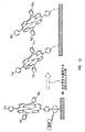
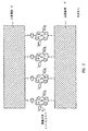
さらなる局面においては、エポキシのようなポリマー材料を含むプリント回路板を提供し、上記ポリマー材料は、実質量の充填剤材料、例えば、ガラス、シリカまたは他の材料を含有し得、その表面上で、ポルフィリンのような化学接着剤材料(金属、限定するものではないが、銅に対する上記ポリマー材料の化学親和性を改変させて上記ポリマー複合体と金属層間の強力な接着を容易にする)によって改変されている。上記化学接着剤層の第2層を上記金属表面に適用して、上記金属表面とその後のポリマー(エポキシ/ガラス)層間の接着を促進させることができる。ある実施態様においては、PCBは、多層導電性構造体である。 In a further aspect, a printed circuit board is provided that includes a polymeric material, such as an epoxy, and the polymeric material may contain a substantial amount of filler material, such as glass, silica, or other material on its surface. Modified by a chemical adhesive material such as porphyrin (metal, but not limited to, modify the chemical affinity of the polymer material to copper to facilitate strong adhesion between the polymer composite and the metal layer) Has been. A second layer of the chemical adhesive layer can be applied to the metal surface to promote adhesion between the metal surface and the subsequent polymer (epoxy / glass) layer. In some embodiments, the PCB is a multilayer conductive structure.
例えば、1つの局面においては、少なくとも1層の金属層、該少なくとも1層の金属層に付着させた有機分子層;および該有機分子上のエポキシ層を含むプリント回路板を提供する。ある実施態様においては、上記少なくとも1層の金属層は、0.5kg/cmよりも高い剥離強度および250nmよりも細かい表面粗さを示す。ある実施態様においては、上記少なくとも1層の金属層は、その上に形成されたパターン化金属線をさらに含み、上記パターン化金属線は、25ミクロン以下の幅を有する。さらに、パターン化金属線は、15ミクロン以下、10ミクロン以下または5ミクロン以下の幅を有する。 For example, in one aspect, a printed circuit board is provided that includes at least one metal layer, an organic molecular layer attached to the at least one metal layer; and an epoxy layer on the organic molecule. In one embodiment, the at least one metal layer exhibits a peel strength greater than 0.5 kg / cm and a surface roughness finer than 250 nm. In one embodiment, the at least one metal layer further includes a patterned metal line formed thereon, and the patterned metal line has a width of 25 microns or less. Further, the patterned metal line has a width of 15 microns or less, 10 microns or less, or 5 microns or less.
本発明のもう1つの局面においては、1層以上の金属層およびその上に形成された1層以上のエポキシ層を有し、上記1層以上の金属層の少なくとも1層が0.5kg/cmよりも高い剥離強度および250nmよりも細かい表面粗さを示すことを特徴とするプリント回路板を提供する。
本発明のさらにもう1つの局面においては、1層以上の金属層および1層以上のエポキシ層を有し、上記1層以上の金属層の少なくとも1層がその上に形成されたパターン化金属線をさらに含み、上記パターン化金属線が25ミクロン以下の幅を有することを特徴とするプリント回路板を提供する。
In another aspect of the present invention, one or more metal layers and one or more epoxy layers formed thereon are provided, and at least one of the one or more metal layers is 0.5 kg / cm or more. The present invention provides a printed circuit board characterized by exhibiting a high peel strength and a surface roughness finer than 250 nm.
In still another aspect of the present invention, the patterned metal wire has one or more metal layers and one or more epoxy layers, and at least one of the one or more metal layers is formed thereon. And the patterned metal line has a width of 25 microns or less.
さらに有利には、本発明の実施態様は、分子を表面上に選択的に接触させて複数の領域またはパターン化領域を形成させ、その後、これらの領域を処理して、その上に、所望の分子または成分、例えば、限定するものではないが、金属または半導体の選択的領域を形成させることによって材料を表面または基板上に選択的に付着させることによる表面の処理方法を提供する。この場合、上記接着剤分子層を、基板の特定領域に、フォトレジストおよび光リソグラフィーを当該技術において通常使用するようにして使用して接触させるか、或いは、上記接着剤分子層を表面全体に適用し、選択的に活性化させる。これは、リソグラフィー法、イオンビーム活性化、または表面の適切な空間イメージングをもたらし得る任意の他の方法による光活性化によって達成し得る。 Even more advantageously, embodiments of the present invention allow molecules to be selectively contacted on a surface to form a plurality of regions or patterned regions, which are then processed to provide a desired A method of treating a surface by selectively depositing a material on a surface or substrate by forming a selective region of molecules or components such as, but not limited to, metal or semiconductor. In this case, the adhesive molecular layer is brought into contact with a specific area of the substrate using photoresist and photolithography as is normally used in the art, or the adhesive molecular layer is applied to the entire surface. And selectively activate. This can be achieved by photoactivation by lithographic methods, ion beam activation, or any other method that can result in proper spatial imaging of the surface.
さらに、本発明の実施態様は、例えば、銅等のような金属元素でめっきすることによって後で処理する表面または基板上での序列分子アッセンブリの形成方法も提供する。
本発明の実施態様は、さらに、1個以上の付着基によって誘導体化された1種以上の耐熱性有機分子;および、興味ある1種以上の分子の表面または基板への結合を促進させる表面処理方法を実施することについての教材を含むキットも提供する。
高密度半導体装置の製造は、この単分子層を、基板上への金属層の付着のためのプレカーサーとして使用することの利益を享受し得る。とりわけ、本発明は、金属層を半導体基板上への電気化学的付着のための方法および系に関する。
本発明の上記および他の局面は、添付図面(同じ参照文字は、同じ部分を示す)と一緒に以下の詳細な説明を検討すれば明白であろう。
Furthermore, embodiments of the present invention also provide a method of forming ordered molecular assemblies on a surface or substrate that is subsequently treated by plating with a metal element such as, for example, copper.
Embodiments of the present invention further include one or more refractory organic molecules derivatized with one or more attachment groups; and a surface treatment that promotes binding of the one or more molecules of interest to the surface or substrate. Kits are also provided that include instructional materials on performing the method.
Fabrication of high density semiconductor devices can benefit from using this monolayer as a precursor for the deposition of a metal layer on a substrate. In particular, the present invention relates to a method and system for electrochemical deposition of a metal layer onto a semiconductor substrate.
These and other aspects of the invention will be apparent upon consideration of the following detailed description, taken in conjunction with the accompanying drawings, in which like reference characters designate like parts.
上記の一般的説明および以下の説明は、共に例示で且つ説明目的のみであり、本明細書において説明する方法および装置を制限するものではないことを理解すべきである。本出願においては、単数形の使用は、特に他で断らない限り、複数形を包含する。また、“または”の使用は、他に断らない限り、“および/または”を意味する。同様に、“含む(comprise)”、“含む(comprises)”、“含む(comprising)”、“含む(include)”、“含む(includes)”、“含む(including)”、“有する(has)”および“有する(having)”も限定を意図するものではない。 It should be understood that both the foregoing general description and the following description are exemplary and explanatory only and are not restrictive of the methods and apparatus described herein. In this application, the use of the singular includes the plural unless specifically stated otherwise. Also, the use of “or” means “and / or” unless stated otherwise. Similarly, “comprise”, “comprises”, “comprising”, “include”, “includes”, “including”, “has” "" And "having" are not intended to be limiting.
1つの局面においては、本発明は、有機分子層のフィルムを種々の基板に結合、付着および/または成長させる方法を提供し、この方法は、従来技術の上述した問題に対する解決法を提供する。
本発明のある実施態様においては、フィルムは、任意の導電性、半導電性または非導電性表面上に、反応基を含む分子の有機溶媒中または水溶液中での熱反応によって形成させる。熱反応は、種々の条件下で実施し得る。本発明の方法は、上記表面または基板上に付着した有機フィルムを生成させ、このフィルムの厚さは、おおよそ1つの分子の単分子層に等しいかまたはこの単分子層よりも厚い。
In one aspect, the present invention provides a method for bonding, attaching and / or growing organic molecular layer films to various substrates, which provides a solution to the above-mentioned problems of the prior art.
In certain embodiments of the invention, the film is formed on any conductive, semiconductive or non-conductive surface by thermal reaction of molecules containing reactive groups in an organic solvent or in an aqueous solution. The thermal reaction can be carried out under various conditions. The method of the present invention produces an organic film deposited on the surface or substrate, the thickness of which is approximately equal to or greater than the monolayer of one molecule.
ある局面においては、本発明は、下記の工程を含むことを特徴とする、1種以上の興味ある分子の表面への結合を促進するための表面処理方法を提供する:
表面を、上記有機分子を表面に付着させるように配置している1個以上の付着基および上記有機分子をその後の興味ある材料に結合するように配置している1個以上の結合基を担持する熱安定性基本成分を含む有機分子と接触させる工程;および、上記有機分子と表面を少なくとも25℃の温度に加熱して、上記有機分子が上記表面に付着し且つその後の興味ある材料との結合に対して増強された親和性を示す工程。
In one aspect, the present invention provides a surface treatment method for promoting the binding of one or more molecules of interest to a surface, comprising the following steps:
The surface carries one or more attachment groups arranged to attach the organic molecule to the surface and one or more binding groups arranged to attach the organic molecule to a material of interest thereafter. Contacting with an organic molecule comprising a thermostable basic component to be heated; and heating the organic molecule and the surface to a temperature of at least 25 ° C. so that the organic molecule adheres to the surface and subsequently with the material of interest Showing enhanced affinity for binding.
もう1つの局面においては、本発明は、1種以上の有機分子を含むコーティングまたはフィルムを提供し、上記有機分子は、熱安定性基本単位、表面に付着するように配置した1個以上の付着基、および1個以上の結合基を含む。とりわけ有利なことに、本発明のコーティングまたはフィルムは、広範囲の装置における表面をコーティングする種々の用途において使用し得る。例えば、上記1個以上の結合基を1種以上の生体適合性化合物に結合するように配置して、生体適合性コーティングを形成させることができる。また、上記1個以上の結合基を、1種以上の親水性化合物に結合するように配置して、親水性コーティングを形成させるか、或いは、逆に、疎水性化合物に結合するように配置して、表面をより疎水性にする。ある実施態様においては、上記1個以上の結合基を1種以上の耐腐蝕性化合物に結合するように配置して、耐腐蝕性コーティングを形成させる。さらなる実施態様においては、上記1個以上の結合基を、光吸収特性を示す1種以上の化合物に結合するように配置する。さらなる局面においては、上記1個以上の結合基を、負の屈折率を示す1種以上の化合物に結合するように配置して、ステルスコーティングを形成させ得る。 In another aspect, the present invention provides a coating or film comprising one or more organic molecules, wherein the organic molecules are one or more attachments arranged to adhere to a heat stable base unit, a surface. Group, and one or more linking groups. Particularly advantageously, the coatings or films of the present invention can be used in a variety of applications for coating surfaces in a wide range of devices. For example, the one or more linking groups can be arranged to bind to one or more biocompatible compounds to form a biocompatible coating. Further, the one or more linking groups are arranged so as to bind to one or more hydrophilic compounds to form a hydrophilic coating, or conversely, arranged so as to bind to a hydrophobic compound. To make the surface more hydrophobic. In one embodiment, the one or more linking groups are arranged to bind to one or more corrosion resistant compounds to form a corrosion resistant coating. In a further embodiment, the one or more linking groups are arranged to bind to one or more compounds that exhibit light absorption properties. In a further aspect, the one or more linking groups can be arranged to bind to one or more compounds exhibiting a negative refractive index to form a stealth coating.
さらに、本発明の方法は、外部媒体に対する、例えば、腐蝕に対する保護を提供すること、および/または上述したような有機官能基を有する付着コーティングを提供すること、および/または処理対象物の表面での導電性を促進または維持することを同時になし得る有機フィルムを製造するのを可能にする。
従って、本発明の方法によって、多層導電性構造体を製造することも、例えば、本発明をベースとする有機挿入フィルムを使用することによって可能である。
Furthermore, the method of the present invention provides protection against external media, eg, corrosion, and / or provides an adhesion coating with organic functional groups as described above, and / or on the surface of the workpiece. This makes it possible to produce an organic film that can simultaneously promote or maintain the conductivity of the film.
Thus, it is also possible to produce multilayer conductive structures by the method of the invention, for example by using an organic insertion film based on the invention.
ある実施態様においては、本発明に従って得られた有機フィルムは、上記有機フィルムを付着させている導電性表面の腐蝕電位よりも高いアノード電位に耐える付着保護コーティングを構成する。
また、本発明の方法は、例えば、相応するビニルモノマーを上記導電性ポリマーフィルム上で熱重合させることによってビニルポリマーを付着させる工程も含み得る。
また、本発明の方法は、極めて強い有機/導電体界面を生成させるのにも使用し得る。とりわけ、本発明の有機フィルムは、如何なる厚さにおいても導電性である。上記有機フィルムは、慎重に架橋させたとき、見掛けの面積が上記有機フィルムを付着させる元の表面よりも極めて大きい導電性表面を有する“導電性スポンジ”を構成し得る。このことは、上記有機フィルムを付着させる出発表面よりも濃密な分子付着を実現することを可能にする。
従って、本発明は、調整可能な厚さを有する付着導電性有機コーティングを導電性または半導電性表面上に生成させるのを可能にする。
In one embodiment, the organic film obtained in accordance with the present invention constitutes an adhesion protective coating that withstands an anode potential that is higher than the corrosion potential of the conductive surface to which the organic film is deposited.
The method of the present invention can also include the step of depositing the vinyl polymer, for example, by thermally polymerizing the corresponding vinyl monomer on the conductive polymer film.
The method of the present invention can also be used to generate very strong organic / conductor interfaces. In particular, the organic film of the present invention is conductive at any thickness. The organic film, when carefully crosslinked, can constitute a “conductive sponge” having a conductive surface whose apparent area is much greater than the original surface to which the organic film is deposited. This makes it possible to achieve denser molecular adhesion than the starting surface to which the organic film is attached.
The present invention thus makes it possible to produce a deposited conductive organic coating having an adjustable thickness on a conductive or semiconductive surface.
本発明の方法は、例えば、非貴金属を化学薬品によって発生する侵食のような外的侵食、例えば、腐蝕等に対して保護するのに使用し得る。本発明の方法によって付与されるこの新規な保護は、例えば、導電特性が改良されおよび/または保持される接続部または接触子においてとりわけ有利であることを証明することができる。 The method of the present invention can be used, for example, to protect non-noble metals against external erosion, such as erosion caused by chemicals, such as corrosion. This novel protection afforded by the method of the present invention can prove particularly advantageous, for example, in connections or contacts where the conductive properties are improved and / or retained.
また、本発明は、さらなる層を金属層に強く付着させるのを可能にする。例えば、分子層を金属基板に付着させる;結合した時点で、この分子層は、さらなる金属層に接着するように或いは絶縁層に付着するように機能する。この方法に対しては、半導体工業(即ち、半導体基板上のバリア金属に付着させた分子層を使用して銅の電気めっきを可能にする)、プリント回路板工業(分子フィルムを銅金属層上に付着させて、後のエポキシまたは他の絶縁層の付着のための接着層として機能させる)、および一般的な製造方法(例えば、金属基板へのプラスチックの付着)における例でもって多くの用途が存在する。 The present invention also allows a further layer to be strongly attached to the metal layer. For example, a molecular layer is attached to a metal substrate; when bonded, the molecular layer functions to adhere to a further metal layer or to an insulating layer. For this method, the semiconductor industry (i.e., enables the electroplating of copper using a molecular layer attached to a barrier metal on a semiconductor substrate), the printed circuit board industry (a molecular film on a copper metal layer). And serve as an adhesive layer for subsequent epoxy or other insulating layer deposition), and many applications with examples in common manufacturing methods (e.g., plastic deposition on metal substrates) Exists.
もう1つの応用においては、本発明の方法は、例えば、全てのタイプ分子付着を実施し得る全てのタイプの導電性または半導電性表面上の付着副層、とりわけ、ビニルモノマー、張力環、ジアゾニウム塩、カルボン酸塩、アルキン、グリニャール誘導体等の、電気化学、例えば、電着または電気付着を使用する付着副層の被覆剤の製造において使用し得る。従って、この副層は、例えば、バイオメディックス、バイオテクノロジー、化学センサー、計装等の分野における対象物の再メタライゼーションのための或いは官能基を付着させるための高品質最終加工を構成する。 In another application, the method of the invention can be used, for example, for adhesion sublayers on all types of conductive or semiconductive surfaces capable of performing all types of molecular adhesion, notably vinyl monomers, tension rings, diazonium. It can be used in the preparation of coatings for deposition sublayers using electrochemistry, for example electrodeposition or electro-deposition, such as salts, carboxylates, alkynes, Grignard derivatives, etc. This sub-layer thus constitutes a high-quality final process for remetallization of objects in the fields of biomedics, biotechnology, chemical sensors, instrumentation, etc. or for attaching functional groups, for example.
さらに、本発明は、そのようにして、例えば、電子部品用のカプセル化コーティングの製造において;親水性コーティングの製造において;生体適合性コーティングの製造において;接着プライマー、として、有機後分子付着支持体として、光吸収特性を有するコーティングとしてまたはステルス特性を有するコーティングとして使用することのできるフィルムの製造において使用し得る。 Furthermore, the present invention thus provides, for example, in the manufacture of encapsulated coatings for electronic components; in the manufacture of hydrophilic coatings; in the manufacture of biocompatible coatings; As a coating having light absorption properties or in the manufacture of a film that can be used as a coating having stealth properties.
1つの応用においては、本発明は、金属の電気めっきのための分子接着層を付与するのに使用し得る。1つの例においては、分子をポリマー、エポキシまたはカーボンコーテッド基板のようなプリント回路基板に付着させて、無電解銅めっきのような金属の無電解めっき用のシード層を提供する。本発明の教示によれば、そのような分子は、有機基板に対する強い結合および/または強い有機‐Cu結合を示す。付着分子の高親和性は、銅の無電解めっきを容易にし、その後、この銅をシード層として使用して大量の銅を電気めっきする。
1つの実施態様においては、上記フィルムは、電気めっきにおいて使用する元素(例えば、Cu、Ni、Pd)の析出を安定化させ、元の表面よりも電気めっき用の適切な基板を提供する。
In one application, the present invention can be used to provide a molecular adhesion layer for metal electroplating. In one example, molecules are attached to a printed circuit board such as a polymer, epoxy or carbon coated substrate to provide a seed layer for electroless plating of a metal such as electroless copper plating. In accordance with the teachings of the present invention, such molecules exhibit strong bonds and / or strong organic-Cu bonds to the organic substrate. The high affinity of the adhesion molecules facilitates electroless plating of copper, and then electroplats large amounts of copper using this copper as a seed layer.
In one embodiment, the film stabilizes the deposition of elements used in electroplating (eg, Cu, Ni, Pd) and provides a more suitable substrate for electroplating than the original surface.
ある実施態様においては、本発明の方法は、上記有機フィルムのプレカーサーである少なくとも1種の熱安定性分子種の以下の工程を含む熱誘発反応によって実施する:上記フィルムを、上記分子種を表面と溶液中または化学蒸着により接触させることによって付着させ、成長させる工程;表面を加熱して、上記分子を表面に結合させる化学反応を誘発させる工程;その後、過剰物を、未反応分子を溶解することのできる溶媒の添加および除去によって洗い落とす工程。この後、さらなる処理、例えば、通常の手順を使用する所望金属の電気めっきを行い得る。付着させた分子は、表面上の金属イオンを安定化し、電気めっきを促進する。また、さらなる処理は、必要でなくてもよい。例えば、上記方法は、適切な基板上での耐腐蝕性コーティングまたは生体適合性コーティングのような最終生成物を形成させ得る。 In one embodiment, the method of the invention is carried out by a heat-induced reaction comprising the following steps of at least one thermostable molecular species that is a precursor of the organic film: the film is surfaced with the molecular species. Adhering and growing by contact with a solution or by chemical vapor deposition; heating the surface to induce a chemical reaction that binds the molecule to the surface; and then dissolving excess and unreacted molecules Washing off by the addition and removal of solvents that can. This can be followed by further processing, for example electroplating of the desired metal using conventional procedures. The attached molecules stabilize the metal ions on the surface and promote electroplating. Further processing may not be necessary. For example, the method can form a final product such as a corrosion resistant coating or a biocompatible coating on a suitable substrate.
1つの局面においては、本発明は、分子種を、限定するものではないが電子材料表面のような表面に付着させることによる表面処理方法を提供する。ある実施態様においては、上記分子としては、ポルフィリンおよび関連種がある。電子材料としては、限定することなしに、ケイ素、酸化ケイ素、窒化ケイ素、金属、金属酸化物、金属窒化物、およびポリマーおよびエポキシのような炭素系材料を含むプリント回路基板がある。他の表面としては、限定することなしに、センサー基板、プラスチックおよびセンサーのような生物医学装置において有用な材料、並びに光起電および太陽電池基板がある。付着手順は、簡単であり、短時間内で終了し得、最低量の材料しか必要とせず、種々の分子官能基と適合性があり、ある場合には、例のない付着モチーフを与える。これらの特性は、めっき過程を終了させるのに必要である処理工程への上記分子物質の組込みを大いに増進させる。 In one aspect, the present invention provides a surface treatment method by attaching molecular species to a surface such as, but not limited to, an electronic material surface. In certain embodiments, the molecules include porphyrins and related species. Electronic materials include, without limitation, printed circuit boards including silicon, silicon oxide, silicon nitride, metals, metal oxides, metal nitrides, and carbon-based materials such as polymers and epoxies. Other surfaces include, without limitation, materials useful in biomedical devices such as sensor substrates, plastics and sensors, and photovoltaic and solar cell substrates. The attachment procedure is simple, can be completed in a short time, requires a minimal amount of material, is compatible with various molecular functional groups, and in some cases gives an unprecedented attachment motif. These properties greatly enhance the incorporation of the molecular material into the processing steps necessary to complete the plating process.
1つの実施態様においては、本発明は、有機分子を、第II、III、IV、VまたはVI族元素の表面に、或いは第II、III、IV、VまたはVI族元素を含む半導体に(より好ましくは、第III、IVまたはV族元素を含む材料に)、或いは遷移金属、遷移金属酸化物もしくは窒化物および/または遷移金属を含む合金に、或いは他の金属にカップリングさせる方法を提供する。 In one embodiment, the present invention provides organic molecules to the surface of a Group II, III, IV, V or VI element or to a semiconductor comprising a Group II, III, IV, V or VI element (more Preferably, a method is provided for coupling to materials containing Group III, IV or V elements), or to transition metals, transition metal oxides or nitrides and / or alloys containing transition metals, or to other metals. .
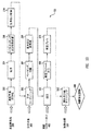
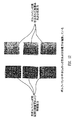
ある実施態様においては、図1Aに一般的に示しているように、本発明は、分子を表面にカップリングさせることによる表面処理方法を提供する。一般に、分子を、“連結(tether)”基を介して、熱、光化学または電気化学活性化によって、基板に付着させる。図1Bは、分子を金属層に付着させ、それによって金属層を改変し、その後、エポキシ基板を改変金属層にラミネートする本発明の典型的な方法100の1つの実施態様を示している。ある実施態様においては、この典型的な方法は、一般に、表面前処理200、分子付着300、真空ラミネート加工400、および必要に応じての加熱処理500を含む。また、図1Bは、上記方法において、剥離強度試験600を実施する場合を示しているが、この工程は、使用する試験手順およびプロトコールを単に例示するために示している。勿論、本発明の広範な方法工程は、剥離強度試験工程600を含まないことを理解すべきである。
In some embodiments, as generally shown in FIG. 1A, the present invention provides a surface treatment method by coupling molecules to a surface. In general, molecules are attached to a substrate via thermal, photochemical or electrochemical activation via “tether” groups. FIG. 1B shows one embodiment of an
再度図1Bに関して、上記方法は、202での必要に応じての基板の予備清浄化、洗浄204、ソフトエッチングおよび状態調節206、およびその後の表面の洗浄および乾燥208によって実施する。この特定の実施態様においては、基板は、その上に形成された金属層を典型的に含む。その後、分子(1種以上)を、金属表面に、302において上記1種以上の分子をコーティングし、付着させ、または基板と接触させ、工程304において必要に応じ基板を加熱またはベーキングして上記分子の基板への付着を促進し、306において基板を洗浄し、必要に応じて後処理することによって付着させる。
Referring again to FIG. 1B, the method is performed by pre-cleaning the substrate as needed at 202, cleaning 204, soft etching and
次に、エポキシ層を、典型的にはラミネート加工によって上記分子層に付着させる。この典型的な実施態様においては、真空ラミネート加工を示しているが、本発明は、何も1つの特定のラミネート加工法に限定するものではない。先ず、エポキシ層を、工程402において上記分子層上で組立て、その後、真空ラミネート加工し(404)、必要に応じての真空プレスを施す(406)。
必要に応じて、後処理、例えば、工程502における硬化および/または後アニーリングのような加熱処理を使用し得る。上記の方法によって形成させた装置は、その後、工程600において示すように、剥離強度について試験し得る。
Next, an epoxy layer is attached to the molecular layer, typically by lamination. In this exemplary embodiment, vacuum lamination is shown, but the invention is not limited to any particular lamination method. First, an epoxy layer is assembled on the molecular layer in
If desired, post-treatment, for example, heat treatment such as curing and / or post-annealing in
ある実施態様においては、上記方法は、表面を必要に応じて清浄化および/または前処理し、付着基を担持する1種以上の耐熱性有機分子をコーティングまたは付着させる工程;上記分子を、熱、光化学または電気化学活性化によって上記表面に付着させる工程(例えば、限定することなしに、この工程は、上記分子(1種以上)または種々の分子の混合物および/または表面を少なくとも約25℃の温度に加熱することによって達成し得る);および、必要に応じて上記表面を後洗浄および/または処理する工程を含む。ある実施態様においては、上記有機分子(1種以上)は、上記表面に電気的にカップリングさせる。他の実施態様においては、上記分子は、上記表面に共有結合させる。上記方法は、必要に応じて、不活性雰囲気(例えば、Ar、N2)下に実施し得る。ある実施態様においては、分子付着は、上記分子(1種以上)を気相まで加熱することを含み、接触は、上記気相を上記表面に接触させることを含む。ある実施態様においては、分子付着は、上記分子(1種以上)および/または上記表面を、上記分子を上記表面に接触させながら加熱することを含む。ある実施態様においては、分子付着は、上記分子(1種以上)を上記表面に適用し、その後、上記分子(1種以上)および/または表面を同時にまたは連続して加熱することを含む。上記有機分子(1種以上)は、溶媒中または乾燥状態で、或いは気相中に、或いは溶媒中でなくて用意し得る。上記分子は、上記表面と、上記分子の溶液中に浸漬することにより、上記分子の溶液をスプレーすることにより、インクジェットプリンティングによりまたは上記分子の上記表面への直接の蒸着等によって接触させ得る。また、本発明の方法は、平坦でない表面上のフィルムまたはコーティングを処理するのに、また、これらのフィルムまたはコーティングを形成するのに適している。例えば、上記有機分子は、パターン化、構造化、湾曲型または他の平坦でない表面および基板に付着させることができる。 In certain embodiments, the method comprises the steps of cleaning and / or pretreating the surface as necessary to coat or attach one or more refractory organic molecules bearing attachment groups; Attaching to the surface by photochemical or electrochemical activation (eg, without limitation, this step may comprise the molecule (s) or a mixture of various molecules and / or the surface at least about 25 ° C. Can be achieved by heating to temperature); and optionally post-cleaning and / or treating the surface. In some embodiments, the organic molecule (s) are electrically coupled to the surface. In another embodiment, the molecule is covalently bound to the surface. The above method may be performed under an inert atmosphere (for example, Ar, N 2 ) as necessary. In some embodiments, molecular attachment includes heating the molecule (s) to the gas phase, and contacting includes contacting the gas phase to the surface. In some embodiments, molecular attachment includes heating the molecule (s) and / or the surface while contacting the molecule with the surface. In some embodiments, molecular attachment includes applying the molecule (s) to the surface and then heating the molecule (s) and / or surface simultaneously or sequentially. The organic molecules (one or more) can be prepared in a solvent or in a dry state, in a gas phase, or not in a solvent. The molecule can be contacted with the surface by dipping in the solution of the molecule, by spraying the solution of the molecule, by ink jet printing or by direct vapor deposition of the molecule on the surface. The method of the present invention is also suitable for treating films or coatings on uneven surfaces and for forming these films or coatings. For example, the organic molecules can be attached to patterned, structured, curved or other uneven surfaces and substrates.
上記分子の結合を熱活性化によって行うある実施態様においては、加熱は、少なくとも約25℃、好ましくは少なくとも約50℃、より好ましくは少なくとも約100℃、最も好ましくは少なくとも約150℃の温度にする。加熱は、任意の好都合な方法、例えば、オーブン内、ホットプレート上、CVD装置内、プラズマ援用CVD装置内、MBE装置内等で行い得る。ある実施態様においては、上記表面は、PCB基板、例えば、限定するものではないが、エポキシ、ガラス強化エポキシ、フェノール、ポリイミド、ガラス強化ポリイミド、シアネート、エステル、テフロン(登録商標)等のようなポリマーおよび炭素材料がある。他の実施態様においては、上記表面は、第III族元素、第IV族元素、第V族元素、第III族元素を含む半導体、第IV族元素を含む半導体、第V族元素を含む半導体、遷移金属および遷移金属酸化物からなる群から選ばれる材料を含む。他の実施態様においては、上記表面は、光起電または太陽電池装置を構成する。ある実施態様においては、上記光起電または太陽電池装置は、ケイ素、結晶性ケイ素、非晶質ケイ素、単結晶性ケイ素、多結晶性ケイ素、微結晶性ケイ素、ナノ結晶性ケイ素、CdTe、銅インジウムガリウムジセリニド(CIGS)、第III〜V族半導体材料、およびこれらの組合せの任意の1種以上からなる表面を含む。 In certain embodiments where the binding of the molecule is effected by thermal activation, the heating is at a temperature of at least about 25 ° C, preferably at least about 50 ° C, more preferably at least about 100 ° C, and most preferably at least about 150 ° C. . Heating can be done in any convenient manner, for example, in an oven, on a hot plate, in a CVD device, in a plasma-assisted CVD device, in an MBE device, or the like. In some embodiments, the surface is a PCB substrate, such as, but not limited to, polymers such as epoxy, glass reinforced epoxy, phenol, polyimide, glass reinforced polyimide, cyanate, ester, Teflon, and the like. And carbon materials. In another embodiment, the surface includes a Group III element, a Group IV element, a Group V element, a semiconductor containing a Group III element, a semiconductor containing a Group IV element, a semiconductor containing a Group V element, A material selected from the group consisting of transition metals and transition metal oxides is included. In another embodiment, the surface constitutes a photovoltaic or solar cell device. In one embodiment, the photovoltaic or solar cell device comprises silicon, crystalline silicon, amorphous silicon, single crystalline silicon, polycrystalline silicon, microcrystalline silicon, nanocrystalline silicon, CdTe, copper It includes a surface comprising any one or more of indium gallium diselinide (CIGS), group III-V semiconductor materials, and combinations thereof.
他の実施態様においては、ある種の好ましい表面は、以下の1種以上を含む:タングステン、タンタルおよびニオブ、Au、Ag、Cu、Al、Ta、Ti、Ru、Ir、Pt、Pd、Os、Mn、Hf、Zr、V、Nb、La、Y、Gd、Sr、Ba、Cs、Cr、Co、Ni、Zn、Ga、In、Cd、Rh、Re、W、Mo、並びにこれらの酸化物、合金、混合物および/または窒化物。ある実施態様においては、上記表面は、第III、第IVもしくは第V族元素、および/またはドープ第III、第IVもしくは第V族元素、例えば、ケイ素、ゲルマニウム、ドープケイ素、ドープゲルマニウム等を含む。上記表面は、必要に応じて、水素不動態化表面であり得る。 In other embodiments, certain preferred surfaces include one or more of the following: tungsten, tantalum and niobium, Au, Ag, Cu, Al, Ta, Ti, Ru, Ir, Pt, Pd, Os, Mn, Hf, Zr, V, Nb, La, Y, Gd, Sr, Ba, Cs, Cr, Co, Ni, Zn, Ga, In, Cd, Rh, Re, W, Mo, and their oxides, Alloys, mixtures and / or nitrides. In some embodiments, the surface comprises a Group III, Group IV or Group V element and / or a doped Group III, Group IV or Group V element, such as silicon, germanium, doped silicon, doped germanium, and the like. . The surface can optionally be a hydrogen passivated surface.
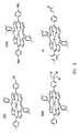
一般に、本発明の有機分子は、図2に示すように、1個以上の結合基Xおよび1個以上の付着基Yを有する熱安定性または耐熱性単位または基本成分からなる。ある実施態様においては、上記耐熱性分子は、以下の任意の1種以上から選ばれる金属結合性分子である:ポルフィリン、ポルフィリン系大員環、拡張ポルフィリン、収縮ポルフィリン、線状ポルフィリンポリマー、ポルフィリン系サンドイッチ配位複合体またはポルフィリンアレー。 In general, the organic molecule of the present invention consists of a heat-stable or heat-resistant unit or basic component having one or more linking groups X and one or more attachment groups Y as shown in FIG. In one embodiment, the heat-resistant molecule is a metal-binding molecule selected from any one or more of the following: porphyrin, porphyrin-based macrocycle, expanded porphyrin, contracted porphyrin, linear porphyrin polymer, porphyrin-based Sandwich coordination complex or porphyrin array.
一般に、ある実施態様においては、上記有機分子は、1個以上の結合基Xおよび1個以上の付着基Yを有する熱安定性の単位または基本成分からなる。ある実施態様においては、上記有機分子は、は、耐熱性金属結合性分子であり、関連出願においては“レドックス活性成分”または“ReAMs”とも称する1種以上の“表面活性成分”からなり得る。本発明の1つの実施態様は、米国特許第6208553号、第6381169号、第6657884号、第6324091号、第6272038号、第6212093号、第6451942号、第6777516号、第6674121号、第6642376号、第6728129号;米国公開公報第20070108438号、第20060092687号、第20050243597号、第20060209587号、第20060195296号、第20060092687号、第20060081950号、第20050270820号、第20050243597号、第20050207208号、第20050185447号、第20050162895号、第20050062097号、第20050041494号、第20030169618号、第20030111670号、第20030081463号、第20020180446号、第20020154535号、第20020076714号、第2002/0180446号、第2003/0082444号、第2003/0081463号、第2004/0115524号、第2004/0150465号、第2004/0120180号、第2002/010589号;U.S.S.N. 10/766,304号、10/834,630号、10/628868号、10/456321号、10/723315号、10/800147号、10/795904号、10/754257号、60/687464号において一般的に説明されている表面活性成分を使用する分子成分の組成物の使用に及ぶ;上記特許は、全て、その全体を本明細書に明確に合体させる。上記で列挙した関連出願においては、上記耐熱性分子は“レドックス活性成分”または“ReAMs”とも称されるけれども、本出願においては、表面活性成分なる用語がより適切であることに留意されたい。一般に、ある実施態様においては、大環状および非大環状成分のような、全て多座プロリガンドをベースとする本発明において有用な数種のタイプの表面活性成分が存在する。多くの適切なプロリガンドおよび複合体、並びに適切な置換基が、上記の引用文献に概略されている。さらに、多くの多座プロリガンドは、置換基(本明細書および上記の引用文献においては、多くの場合“R”基と称している)を含み得、米国特許公開公報第2007/0108438号に概略されている成分および定義を含み得る(上記公報は、とりわけ置換基の定義について本明細書に参考として合体させる)。 In general, in some embodiments, the organic molecule consists of a thermostable unit or base component having one or more linking groups X and one or more attachment groups Y. In one embodiment, the organic molecule is a refractory metal binding molecule and may consist of one or more “surface active ingredients”, also referred to as “redox active ingredients” or “ReAMs” in related applications. One embodiment of the present invention is described in U.S. Pat. Nos. 6,208,553, 6,381,169, 6,665,884, 6,632,4091, 6272038, 621,093, 6,645,1942, 6777516, 6,674121, 6642376. No. 6728129; U.S. Publication No. 20070108438, No. 20060092687, No. 20050243597, No. 20060209587, No. 20060195296, No. 20060092687, No. 20060081950, No. 20050270820, No. 20050243597, No. 20050207208, No. 20050185447 20050162895, 20050062097, 20050041494, 20030169618, 20030111670, 20030081463, 20020180446, 20020154535, 20020076714, 2002/0180446, 2003/0082444, 2003/0081463, 2004/0115524, 2004/0150465, 2004/0120180, 2002/010589; USSN 10 / 766,304, 10 / 834,630, 10/628868, 10/456321 Surface active ingredients generally described in 10/723315, 10/800147, 10/795904, 10/754257, 60/687464 All of the above patents are expressly incorporated herein in their entirety, extending to the use of the composition of molecular components used. Note that in the above-listed related applications, the thermostable molecules are also referred to as “redox active ingredients” or “ReAMs”, but in this application the term surface active ingredient is more appropriate. In general, in certain embodiments, there are several types of surface active components useful in the present invention, all based on multidentate proligands, such as macrocyclic and non-macrocyclic components. Many suitable proligands and conjugates, and suitable substituents are outlined in the above cited references. In addition, many multidentate proligands can contain substituents (often referred to herein as "R" groups) and in US Patent Publication No. 2007/0108438. The components and definitions outlined may be included (the above publication is specifically incorporated herein by reference for the definition of substituents).
適切なプロリガンドは、以下の2つのカテゴリーに分類される:窒素、酸素、イオウ、炭素またはリン原子(金属イオンに応じる)を配位原子(文献においてはシグマ(a)ドナーと一般に称されている)として使用するリガンド類、およびメタロセンリガンドのような有機金属リガンド(文献においてはpiドナーと一般に称されており、米国特許公開公報第2007/0108438号においてはLmとして示されている)。
さらに、1つの表面活性成分は、例えば、ポルフィリンおよびフェロセン類を使用している米国特許公開公報第2007/0108438号の図13Aに示されているように、2個以上のレドックス活性サブユニットを有し得る。
Suitable proligands fall into two categories: Nitrogen, oxygen, sulfur, carbon or phosphorus atoms (depending on the metal ion) are coordinated atoms (commonly referred to in the literature as sigma (a) donors). And organometallic ligands such as metallocene ligands (commonly referred to in the literature as pi donors and shown as Lm in US Patent Publication No. 2007/0108438).
In addition, one surface active component has two or more redox active subunits as shown, for example, in FIG. 13A of US Patent Publication No. 2007/0108438 using porphyrins and ferrocenes. Can do.
ある実施態様においては、上記表面活性成分は、大環状リガンドであり、これには、大環状プロリガンドおよび大環状複合体の双方がある。“大環状プロリガンド”とは、本明細書においては、金属イオンに結合するように配向させたドナー原子(“配位原子”とも称する)を含有し且つ金属原子を取囲むのに十分に大きい環状化合物を意味する。一般に、上記ドナー原子は、限定するものではないが窒素、酸素およびイオウのようなヘテロ原子であり、前者がとりわけ好ましい。しかしながら、当業者であれば認識しているように、異なる金属イオンは、異なるヘテロ原子に優先して結合し、従って、使用するヘテロ原子は、所望する金属イオンに応じ得る。さらに、ある実施態様においては、1つの大員環は、種々のタイプのヘテロ原子を含有し得る。 In certain embodiments, the surface active component is a macrocyclic ligand, which includes both macrocyclic proligands and macrocyclic complexes. “Macrocyclic proligand” as used herein contains a donor atom oriented to bind to a metal ion (also referred to as a “coordinating atom”) and is large enough to surround the metal atom A cyclic compound is meant. In general, the donor atom is a heteroatom such as, but not limited to, nitrogen, oxygen and sulfur, with the former being particularly preferred. However, as one skilled in the art will recognize, different metal ions bind preferentially to different heteroatoms, and thus the heteroatoms used can depend on the desired metal ion. Further, in certain embodiments, one macrocycle may contain various types of heteroatoms.
“大環状複合体”は、少なくとも1種の金属イオンを有する大環状プロリガンドである;ある実施態様においては、大環状複合体は、単一の金属イオンを含むが、以下で説明するように、多核大環状複合体のような多核複合体も意図する。 A “macrocycle complex” is a macrocyclic proligand having at least one metal ion; in certain embodiments, a macrocycle complex comprises a single metal ion, but as described below Also contemplated are multinuclear complexes, such as multinuclear macrocyclic complexes.
電子的に共役させている大環状リガンドおよびそうではあり得ない大環状リガンドのような広範囲の大環状リガンドにおいて、本発明における使用を見出している。適切な大環状リガンドの広範な概略図が、米国特許公開公報第2007/0108438号の図15に示され、説明されている。ある実施態様においては、その環、結合および置換基は、電子的に共役させている化合物を生じるように、また、最低でも少なくとも2つの酸化状態を有するように選定する。 A wide variety of macrocyclic ligands have been found for use in the present invention, such as electronically conjugated macrocyclic ligands and macrocycles that cannot be. An extensive schematic of a suitable macrocyclic ligand is shown and described in FIG. 15 of US Patent Publication No. 2007/0108438. In certain embodiments, the rings, bonds, and substituents are selected to yield an electronically conjugated compound and to have at least two oxidation states.
ある実施態様においては、本発明の大環状リガンドは、ポルフィリン類(とりわけ、下記で定義するようなポルフィリン誘導体)およびシクレン(cyclen)誘導体からなる群から選ばれる。本発明において適する大員環のとりわけ好ましいサブセットは、ポルフィリン誘導体を含むポルフィリン類である。そのような誘導体としては、ポルフィリン核心にオルソ縮合またはオルソペリ縮合させた追加環を有するポルフィリン類、ポルフィリンの1個以上の炭素原子の他の元素の原子による置換(骨格置換)を有するポルフィリン類、ポルフィリン環の窒素原子の他の元素の原子による置換(窒素の骨格置換)を有する誘導体、ポルフィリンの周辺メソ‐、3‐またはコア原子に位置した水素以外の置換基を有する誘導体、ポルフィリンの1以上の結合の飽和を含む誘導体(ヒドロポルフィリン類、例えば、クロリン類、バクテリオクロリン類、イソバクテリオクロリン類、デカヒドロポルフィリン類、コルフィン類、ピロコルフィン類等)、ポルフィリン環中に挿入したピロールまたはピロメテニル単位のような1個以上の原子を有する誘導体(拡張ポルフィリン)、ポルフィリン環から除去した1個以上の基を有する誘導体(収縮ポルフィリン類、例えば、コリン、コロール)、および上記誘導体の組合せ(例えば、フタロシアニン類、サブ‐フタロシアニン類およびポルフィリン異性体)がある。さらなる適切なポルフィリン誘導体としては、限定するものではないが、エチオフィリン(etiophyllin)、ピロポルフィリン、ロードポルフィリン、フィロポルフィリン、フィロエリトリン、クロロフィルaおよびbのようなクロロフィル群;並びに、デューテロポルフィリン、デューテロヘミン、ヘミン、ヘマチン、プロトポルフィリン、メソヘミン、ヘマトポルフィリン、メソポルフィリン、コプロポルフィリン、ウルポルフィリン(uruporphyrin)およびツラシン(turacin)のようなヘモグロビン群;および、テトラアリールアザジピロメチン類の群がある。 In one embodiment, the macrocyclic ligand of the present invention is selected from the group consisting of porphyrins (especially porphyrin derivatives as defined below) and cyclen derivatives. A particularly preferred subset of macrocycles suitable in the present invention are porphyrins including porphyrin derivatives. Such derivatives include porphyrins having additional rings ortho-ortho-peri-condensed at the core of the porphyrin, porphyrins having substitution (skeletal substitution) of one or more carbon atoms of the porphyrin with atoms of other elements, porphyrin One or more derivatives of the ring nitrogen atom with substitution of other element atoms (nitrogen skeleton substitution), porphyrin peripheral meso-, 3- or core-atom-substituted substituents other than hydrogen Derivatives containing bond saturation (e.g. hydroporphyrins, e.g. chlorins, bacteriochlorins, isobacteriochlorins, decahydroporphyrins, colfins, pyrocorphines, etc.), such as pyrrole or pyromethenyl units inserted into the porphyrin ring Derivatives with more than one atom (extended porph Phosphorus), derivatives having one or more groups removed from the porphyrin ring (contracted porphyrins, eg choline, corrole), and combinations of the above derivatives (eg phthalocyanines, sub-phthalocyanines and porphyrin isomers) . Further suitable porphyrin derivatives include, but are not limited to, chlorophyll groups such as etiophyllin, pyroporphyrin, rhodoporphyrin, philoporphyrin, phyloerythrin, chlorophyll a and b; and deuteroporphyrin, dew There is a group of hemoglobins such as telohemin, hemin, hematin, protoporphyrin, mesohemin, hematoporphyrin, mesoporphyrin, coproporphyrin, uruporphyrin and turacin; and a group of tetraarylazadipyrometins .
当業者であれば認識しているように、各不飽和位置は、炭素またはヘテロ原子のいずれであれ、その系の所望の結合価に応じて、本明細書において定義するような1個以上の置換基を有し得る。 As one skilled in the art will recognize, each unsaturation position, whether carbon or heteroatom, depends on the desired valency of the system and includes one or more as defined herein. It may have a substituent.
さらに、“ポルフィリン”の定義内には、ポルフィリンプロリガンドおよび少なくとも1種の金属イオンを含むポルフィリン複合体も包含される。ポルフィリン化合物における適切な金属は、配位原子として使用するヘテロ原子によるが、一般的には、遷移金属イオンから選択する。本明細書において使用するときの用語“遷移金属”は、典型的には、周期律表の第3〜12族内の38の元素を称する。典型的には、遷移金属は、その価電子、即ち、遷移金属が他の元素と結合するのに使用する電子が2以上のシェル内に存在し、結果として、多くの場合、幾つかの共通酸化状態を示すという事実に特徴を有する。ある実施態様においては、本発明の遷移金属としては、限定するものではないが、スカンジウム、チタン、バナジウム、クロム、マンガン、鉄、コバルト、ニッケル、銅、亜鉛、イットリウム、ジルコニウム、ニオブ、モリブデン、テクネチウム、ルテニウム、ロジウム、パラジウム、銀、カドミウム、ハフニウム、タンタル、タングステン、レニウム、オスミウム、イリジウム、白金、パラジウム、金、水銀、ラザホージウムの1種以上;および/またはこれらの酸化物、および/またはこれらの窒化物、および/またはこれらの合金、および/またはこれらの混合物がある。 Further included within the definition of “porphyrin” are porphyrin complexes comprising a porphyrin proligand and at least one metal ion. Suitable metals in the porphyrin compounds depend on the heteroatoms used as coordination atoms, but are generally selected from transition metal ions. The term “transition metal” as used herein typically refers to the 38 elements within Groups 3-12 of the Periodic Table. Typically, transition metals have their valence electrons, ie, the electrons that the transition metal uses to bond with other elements, in two or more shells, and as a result, often have some common Characterized by the fact that it exhibits an oxidation state. In some embodiments, transition metals of the present invention include, but are not limited to, scandium, titanium, vanadium, chromium, manganese, iron, cobalt, nickel, copper, zinc, yttrium, zirconium, niobium, molybdenum, technetium. , Ruthenium, rhodium, palladium, silver, cadmium, hafnium, tantalum, tungsten, rhenium, osmium, iridium, platinum, palladium, gold, mercury, rutherfordium; and / or their oxides and / or their There are nitrides and / or alloys thereof and / or mixtures thereof.
また、シクレン誘導体をベースとする多くの大員環も存在する。米国特許公開公報第2007/0108438号の図17 13Cは、大まかにはシクレン/シクラム誘導体をベースとする多くの大環状プロリガンドを示しており、これらは、個々に選択した炭素またはヘテロ原子の包含による骨格拡張を含み得る。ある実施態様においては、少なくとも1個のR基は、好ましくは金属に電子的に共役させた表面活性サブユニットである。ある実施態様においては、少なくとも1個のR基が表面活性サブユニットである場合に、2個以上の隣接R2基を包含させることによって、シクロまたはアリール環が形成される。本発明においては、上記少なくとも1個のR基は、表面活性サブユニットまたは成分である。 There are also many macrocycles based on cyclene derivatives. FIG. 17 13C of US Patent Publication No. 2007/0108438 shows a number of macrocyclic proligands based roughly on cyclen / cyclam derivatives, which contain individually selected carbon or heteroatoms. May include skeletal expansion. In some embodiments, at least one R group is a surface active subunit, preferably electronically conjugated to a metal. In certain embodiments, when at least one R group is a surface active subunit, inclusion of two or more adjacent R2 groups forms a cyclo or aryl ring. In the present invention, the at least one R group is a surface active subunit or component.
さらにまた、ある実施態様においては、大環状複合体依存性有機金属リガンドを使用する。表面活性成分として使用するための純粋な有機化合物および複素環または環外置換基としてドナー原子を有する8‐結合有機リガンドを含む各種遷移金属配位複合体以外に、pi結合有機リガンドを含む広範囲の遷移金属有機金属化合物が利用可能である (Advanced Inorganic Chemistry, 5th Ed., Cotton & Wilkinson, John Wiley & Sons, 1988, chapter 26;Organometallics, A Concise Introduction, Elschenbroich et al., 2nd Ed., 1992, 30 VCH;および、Comprehensive Organometallic Chemistry II, A Review of the Literature 1982-1994, Abel et al. Ed., Vol. 7, chapters 7, 8, 1.0 & 11, Pergamon Pressを参照されたい;参考として本明細書に明確に合体させる)。そのような有機金属リガンドとしては、シクロペンタジエニドイオン[C5H5(−1)]のような環状芳香族化合物、およびビス(シクロペンタジエイル)金属化合物(即ち、メタロセン類)の群をもたらすインデニリド(−1)のような各種環置換および環縮合誘導体がある;例えば、Robins et al., J. Am. Chem. Soc. 104:1882-1893 (1982)、およびGassman et al., J. Am. Chem. Soc. 108:4228-4229 (1986)を参照されたい(参考として本明細書に合体させる)。これらのうち、フェロセン[(C5H5)2Fe]およびその誘導体は、原型的な例であり、広範囲の化学反応(Connelly et al., Chem. Rev. 96:877-910 (1996);参考として本明細書に合体させる)および電気化学反応(Geiger et al., Advances in Organometallic Chemistry 23:1-93、およびGeiger et al., Advances in Organometallic Chemistry 24:87;参考として本明細書に合体させる)において使用されている。他の潜在的に適切な有機金属リガンドとしては、ビス(ベンゼン)クロムが原型的な例である、ビス(アレーン)金属化合物およびその環置換および環縮合誘導体をもたらすベンゼンのような環状アレーン類がある。アリル(-1)イオンまたはブタジエンのような他の非環式n‐結合リガンドは潜在的に適切な有機金属化合物をもたらし、そのようなリガンドは、全て、他の7c‐結合および8‐結合リガンドとともに、炭素結合に対して金属が存在する一般的な群の有機金属化合物を構成する。架橋有機リガンドおよびさらなる非架橋リガンドを有する、さらにまた、金属‐金属結合を有するまたは有さないそのような化合物の各種ダイマーおよびオリゴマーの電気化学試験は、全て有用である。
Furthermore, in some embodiments, a macrocyclic complex-dependent organometallic ligand is used. In addition to a variety of transition metal coordination complexes that include pure organic compounds for use as surface active components and 8-linked organic ligands that have a donor atom as a heterocyclic or exocyclic substituent, a wide range of pi-linked organic ligands are included. Transition metal organometallic compounds are available (Advanced Inorganic Chemistry, 5th Ed., Cotton & Wilkinson, John Wiley & Sons, 1988, chapter 26; Organometallics, A Concise Introduction, Elschenbroich et al., 2nd Ed., 1992, 30 VCH; and Comprehensive Organometallic Chemistry II, A Review of the Literature 1982-1994, Abel et al. Ed., Vol. 7,
ある実施態様においては、上記表面活性成分は、サンドイッチ配位複合体である。用語“サンドイッチ配位化合物”または“サンドイッチ配位複合体”とは、式L‐Mn‐Lの化合物を称し、式中、各Lは複素環リガンド(下記で説明するような)であり、各Mは金属であり、nは2以上、最も好ましくは2または3であり、各金属が、対のリガンド間に位置して、各リガンド内の1個以上のヘテロ原子(典型的には、複数のヘテロ原子、例えば、2個、3個、4個、5個)に結合している(金属の酸化状態による)。従って、サンドイッチ配位化合物は、金属が炭素原子に結合しているフェロセンのような有機金属化合物ではない。サンドイッチ配位化合物中のリガンドは、一般に、積み重ね配向で配置されている(即ち、一般的に共平面的に配向し、互いに軸方向に整列されているが、これらのリガンドは、互いに対してその軸の周りを回転し得るかまたは回転し得ない(例えば、Ng and Jiang (1997) Chemical Society Reviews 26: 433-442を参照されたい;参考として本明細書に合体させる)。サンドイッチ配位複合体としては、限定するものではないが、“2層サンドイッチ配位化合物”または“3層サンドイッチ配位化合物”がある。サンドイッチ配位化合物の合成および使用は、米国特許第6,212,093号、第6,451,942号、第6,777,516号に詳細に記載されており、これら分子の重合は、WO 2005/086826号に記載されている;それらの記載の全て、とりわけ、サンドイッチ複合体および“単一大員環”複合体中での使用が見出される個々の置換基は、本明細書に含ませる。 In certain embodiments, the surface active component is a sandwich coordination complex. The term “sandwich coordination compound” or “sandwich coordination complex” refers to a compound of formula L-Mn-L, where each L is a heterocyclic ligand (as described below) and each M is a metal, n is 2 or more, most preferably 2 or 3, and each metal is located between a pair of ligands and contains one or more heteroatoms (typically multiple (For example, 2, 3, 4, or 5) (depending on the oxidation state of the metal). Thus, sandwich coordination compounds are not organometallic compounds such as ferrocene where the metal is bonded to a carbon atom. The ligands in a sandwich coordination compound are generally arranged in a stacked orientation (i.e., generally coplanarly oriented and axially aligned with each other, but these ligands are Can or may not rotate about an axis (see, eg, Ng and Jiang (1997) Chemical Society Reviews 26: 433-442; incorporated herein by reference) Sandwich coordination complexes These include, but are not limited to, “two-layer sandwich coordination compounds” or “three-layer sandwich coordination compounds.” The synthesis and use of sandwich coordination compounds is described in US Pat. Nos. 6,212,093, 6,451,942, No. 6,777,516 is described in detail, and the polymerization of these molecules is described in WO 2005/086826; all of those descriptions, inter alia, sandwich complexes and “single macrocycle” complexes. Individual substituents that find use in coalescence are included herein.
さらに、これらのサンドイッチ化合物のポリマーも有用である;これには、U.S.S.N 6,212,093号、6,451,942号、6,777,516号に記載されているような“二分子体(diad)”および“三分子体(triad)”;および、WO 2005/086826号に記載されているようなこれら分子の重合がある;これらの全てを、参考として本発明に合体させ含ませる。
非大環状キレート化剤を含む表面活性成分は、金属の存在が複数のプロリガンドが一緒に結合して複数の酸化状態をもたらすことから、金属イオンと結合させて非大環状キレート化合物を形成させる。
In addition, polymers of these sandwich compounds are also useful; such as “diad” and “triad” as described in USSN 6,212,093, 6,451,942, 6,777,516. And polymerization of these molecules as described in WO 2005/086826; all of which are incorporated into the present invention and incorporated by reference.
Surface active ingredients that include non-macrocyclic chelating agents bind to metal ions to form non-macrocyclic chelating compounds because the presence of the metal binds multiple proligands together resulting in multiple oxidation states .
ある実施態様においては、窒素供与プロリガンドを使用する。適切な窒素供与プロリガンドは、当該技術において周知であり、限定するものではないが、NH2;NFIR;NRR';ピリジン;ピラジン;イソニコチンアミド;イミダゾール;ビピリジンおよびビピリジンの置換誘導体;ターピリジンおよび置換誘導体;フェナントロリン類、とりわけ、1,10‐フェナントロリン(phenと略記する)および4,7‐ジメチルフェナントロリンおよびジピリドール[3,2‐a:2',3'‐c]フェナジン(dppzと略記する)のようなフェナントロリンの置換誘導体;ジピリドフェナジン;1,4,5,8,9,12‐ヘキサアザトリフェニレン(hatと略記する);9,10‐フェナントレンキノンジイミド(phiと略記する);1,4,5,8‐テトラアザフェナントレン(tapと略記する);1,4,8,11‐テトラ‐アザシクロテトラデカン(cyclamと略記する)およびイソシアニドがある。また、縮合誘導体のような置換誘導体も使用し得る。金属イオンを配位的に飽和させてなく、他のプロリガンドの添加を必要とする大環状リガンドは、本目的においては非大環状とみなすことに留意すべきである。当業者であれば認識しているように、多数の“非大環状”リガンドを共有結合させて配位的に飽和の化合物を形成させることは可能であるが、これは環状骨格を欠いている。 In some embodiments, a nitrogen donating proligand is used. Suitable nitrogen donating proligands are well known in the art and include, but are not limited to, NH2; NFIR; NRR '; pyridine; pyrazine; isonicotinamide; imidazole; substituted derivatives of bipyridine and bipyridine; Phenanthrolines, especially 1,10-phenanthroline (abbreviated phen) and 4,7-dimethylphenanthroline and dipyridol [3,2-a: 2 ', 3'-c] phenazine (abbreviated dppz) Substituted phenanthroline derivatives; dipyridophenazine; 1,4,5,8,9,12-hexaazatriphenylene (abbreviated as hat); 9,10-phenanthrenequinone diimide (abbreviated as phi); , 5,8-tetraazaphenanthrene (abbreviated as tap); 1,4,8,11-tetra-azacyclotetradecane (abbreviated as cyclam) and isocyanide. Substituted derivatives such as condensed derivatives can also be used. It should be noted that macrocyclic ligands that do not coordinately saturate the metal ion and require the addition of other proligands are considered non-macrocyclic for this purpose. As one skilled in the art will recognize, many “non-macrocyclic” ligands can be covalently linked to form a coordinately saturated compound, which lacks a cyclic skeleton. .
炭素、酸素、イオウおよびリンを使用する適切なシグマ供与リガンドは、当該技術において知られている。例えば、適切なシグマ炭素ドナーは、Cotton and Wilkenson, Advanced Organic Chemistry, 5th Edition, John Wiley & Sons, 1988において見出される;例えば、38ページを参照されたい、該文献は、参考として本明細書に合体させる。同様に、適切な酸素リガンドとしては、クラウンエーテル、水および当該技術において既知の他のリガンドがある。また、ホスフィンおよび置換ホスフィンも適している; CottonおよびWilkensonの38ページを参照されたい。
酸素, イオウ, リンおよび窒素供与リガンドは、ヘテロ原子を配位原子として機能せしめるような方法で付着させる。
Suitable sigma donating ligands using carbon, oxygen, sulfur and phosphorus are known in the art. For example, suitable sigma carbon donors are found in Cotton and Wilkenson, Advanced Organic Chemistry, 5th Edition, John Wiley & Sons, 1988; see, eg, page 38, which is incorporated herein by reference. Let Similarly, suitable oxygen ligands include crown ethers, water and other ligands known in the art. Phosphine and substituted phosphines are also suitable; see Cotton and Wilkenson, page 38.
Oxygen, sulfur, phosphorus and nitrogen donor ligands are attached in such a way as to make the heteroatom function as a coordinating atom.
さらに、ある実施態様では、多核形成性リガンドである多座リガンドを使用する、例えば、これらのリガンドは、2種以上の金属イオンを結合し得る。これらは、大環状または非大環状であり得る。
また、上記分子成分も、本発明においては、上記で概略したような表面活性成分のポリマーを含み得る;例えば、ポルフィリンポリマー(ポルフィリン複合体のポリマーを包含する)、大員環複合体ポリマー、2種の表面活性サブユニットを含む表面活性成分等を使用することができる。上記ポリマーは、ホモポリマーまたはヘテロポリマーであり得、単量体表面活性成分の任意の多くの種々の混合物(混在物)を含み得る;また、“モノマー”も2種以上のサブユニットを含む表面活性成分(例えば、サンドイッチ配位化合物、1種以上のフェロセンで置換されたポルフィリン誘導体等)を含み得る。表面活性成分ポリマーは、WO 2005/086826号に記載されており、該文献は、その全体を参考として本明細書に合体させる。
Further, in certain embodiments, multidentate ligands that are multinucleating ligands are used, eg, these ligands can bind two or more metal ions. These can be macrocyclic or non-macrocyclic.
The molecular component may also comprise a surface active component polymer as outlined above in the present invention; for example, porphyrin polymers (including porphyrin complex polymers), macrocycle complex polymers, 2 A surface active component containing a surface active subunit of a species can be used. The polymer can be a homopolymer or a heteropolymer, and can include any of a number of different mixtures (mixtures) of monomeric surface active ingredients; a “monomer” also includes a surface that includes two or more subunits. It may contain active ingredients (eg sandwich coordination compounds, porphyrin derivatives substituted with one or more ferrocenes, etc.). Surface active component polymers are described in WO 2005/086826, which is incorporated herein by reference in its entirety.
ある実施態様においては、上記付着基Yは、アリール官能基および/またはアルキル付着基を含む。ある実施態様においては、アリール官能基は、アミノ、アルキルアミノ、ブロモ、ヨード、ヒドロキシ、ヒドロキシメチル、ホルミル、ブロモメチル、ビニル、アリル、S‐アセチルチオメチル、Se‐アセチルセレノメチル、エチニル、2‐(トリメチルシリル)エチニル、メルカプト、メルカプトメチル、4,4,5,5‐テトラメチル‐1,3,2‐ジオキサボロラン‐2‐イル、およびジヒドロキシホスホリルからなる群から選ばれる官能基を含む。ある実施態様においては、アルキル付着基は、ブロモ、ヨード、ヒドロキシ、ホルミル、ビニル、メルカプト、セレニル、S‐アセチルチオ、Se‐アセチルセレノ、エチニル、2‐(トリメチルシリル)エチニル、4,4,5,5‐テトラメチル‐1,3,2‐ジオキサボロラン‐2‐イルおよびジヒドロキシホスホリルからなる群から選ばれる官能基を含む。ある実施態様においては、上記付着基は、アルコールまたはホスホネートを含む。 In some embodiments, the attachment group Y comprises an aryl functional group and / or an alkyl attachment group. In some embodiments, the aryl functionality is amino, alkylamino, bromo, iodo, hydroxy, hydroxymethyl, formyl, bromomethyl, vinyl, allyl, S-acetylthiomethyl, Se-acetylselenomethyl, ethynyl, 2- ( It contains a functional group selected from the group consisting of (trimethylsilyl) ethynyl, mercapto, mercaptomethyl, 4,4,5,5-tetramethyl-1,3,2-dioxaborolan-2-yl, and dihydroxyphosphoryl. In some embodiments, the alkyl attachment group is bromo, iodo, hydroxy, formyl, vinyl, mercapto, selenyl, S-acetylthio, Se-acetylseleno, ethynyl, 2- (trimethylsilyl) ethynyl, 4,4,5,5 -Containing functional groups selected from the group consisting of -tetramethyl-1,3,2-dioxaborolan-2-yl and dihydroxyphosphoryl. In some embodiments, the attachment group comprises an alcohol or phosphonate.
ある実施態様においては、接触工程は、上記有機分子を表面のある領域に選択的に接触させ、他の領域には接触させないことを含む。例えば、接触は、上記有機分子を表面のある領域に選択的に接触させ、他の領域には接触させないことを含み得る。ある実施態様においては、接触は、保護コーティング(例えば、マスキング材料)を、上記有機分子(1種以上)を付着させない領域の表面上に置き;上記分子(1種以上)を上記表面と接触させ;上記保護コーティングを除去して上記有機分子(1種以上)の無い表面領域をもたらす工程を含む。ある実施態様においては、接触は、上記有機分子(1種以上)を含む溶液または乾燥有機分子(1種以上)の表面への接触プリンティングを含む。ある実施態様においては、接触は、表面上に、上記有機分子(1種以上)を含む溶液をスプレーまたは滴下する或いは乾燥有機分子(1種以上)を適用することを含む。ある実施態様においては、接触は、表面を上記有機分子(1種以上)と接触させ、その後、表面の選定した領域をエッチングして上記有機分子(1種以上)を除去することを含む。ある実施態様においては、接触は、分子線エピタキシー(MBE)、および/または化学蒸着(CVD)、および/またはプラズマ援用蒸着、および/またはスパッタリング等を含む。ある実施態様においては、上記耐熱性有機分子は、少なくとも2種の異なる種の耐熱性有機分子の混合物を含み、加熱は、上記混合物および/または表面を加熱することを含む。 In some embodiments, the contacting step includes selectively contacting the organic molecules with certain areas of the surface and not contacting other areas. For example, contacting can include selectively contacting the organic molecule with an area on the surface and not contacting another area. In some embodiments, the contact places a protective coating (eg, a masking material) on the surface of the area where the organic molecule (s) are not attached; the molecule (s) are contacted with the surface. Removing the protective coating to provide a surface area free of the organic molecules (one or more). In some embodiments, the contact includes contact printing on the surface of a solution containing the organic molecule (s) or a dry organic molecule (s). In some embodiments, contacting comprises spraying or dropping a solution containing the organic molecule (s) on the surface or applying dry organic molecule (s). In some embodiments, contacting comprises contacting a surface with the organic molecule (s) and then etching a selected region of the surface to remove the organic molecule (s). In some embodiments, the contact includes molecular beam epitaxy (MBE), and / or chemical vapor deposition (CVD), and / or plasma assisted deposition, and / or sputtering. In some embodiments, the refractory organic molecule comprises a mixture of at least two different species of refractory organic molecules, and heating comprises heating the mixture and / or the surface.
また、本発明は、金属結合性分子(または、種々の種の金属結合性分子の収集物)を表面にカップリングさせる方法を提供する。ある実施態様においては、上記方法は、上記有機分子(1種以上)を気相に加熱する工程;および、上記有機分子(1種以上)を表面に接触させ、それによって上記金属結合性分子(1種以上)が表面にカップリングする工程を含む。ある実施態様においては、上記金属結合性分子を表面に化学的にカップリングさせ、および/または表面に電気的にカップリングさせる。ある実施態様においては、加熱は、少なくとも約25℃、好ましくは少なくとも約50℃、より好ましくは少なくとも約100℃、最も好ましくは少なくとも約150℃の温度にである。加熱は、任意の好都合な方法、例えば、オーブン内、ホットプレート上、加熱炉内、高速加熱炉内、CVD装置内、プラズマ援用CVD装置内、MBE装置内等で行い得る。 The present invention also provides a method of coupling metal binding molecules (or collections of various types of metal binding molecules) to a surface. In some embodiments, the method comprises heating the organic molecule (s) to the gas phase; and contacting the organic molecule (s) to a surface, thereby forming the metal binding molecule ( Including one or more) coupling to the surface. In some embodiments, the metal binding molecule is chemically coupled to the surface and / or electrically coupled to the surface. In certain embodiments, the heating is at a temperature of at least about 25 ° C, preferably at least about 50 ° C, more preferably at least about 100 ° C, and most preferably at least about 150 ° C. Heating can be performed in any convenient manner, for example, in an oven, on a hot plate, in a heating furnace, in a fast heating furnace, in a CVD apparatus, in a plasma-assisted CVD apparatus, in an MBE apparatus, or the like.
ある実施態様においては、表面は、上述したように、第III族元素、第IV族元素、第V族元素、第III族元素を含む半導体、第IV族元素を含む半導体、第V族元素を含む半導体、遷移金属、遷移金属酸化物、プラスチック材料、エポキシ、セラミック、炭素材料等からなる群から選ばれる材料を含み得る。ある実施態様においては、上記表面は、Au、Ag、Cu、Al、Ta、Ti、Ru、Ir、Pt、Pd、Os、Mn、Hf、Zr、V、Nb、La、Y、Gd、Sr、Ba、Cs、Cr、Co、Ni、Zn、Ga、In、Cd、Rh、Re、W、Mo、および/またはこれらの酸化物、窒化物、混合物または合金のような材料を含む。ある実施態様においては、上記金属結合性分子としては、限定するものではないが、本明細書において説明している任意の分子がある。同様に、上記付着基としては、限定するものではないが、本明細書において説明している任意の付着基がある。ある実施態様においては、第II、III、IV、VまたはVI族元素;より好ましくは、第III、IVまたはV族元素;さらにより好ましくは、第IV族元素またはドープ化第IV族元素(例えば、ケイ素、ゲルマニウム、ドープケイ素、ドープゲルマニウム等)。ある実施態様においては、接触は、揮発させた上記有機分子を表面のある領域に選択的に接触させ、他の領域には接触させないことを含む。ある実施態様においては、接触は、保護コーティングを、上記金属結合性分子を付着させない領域の表面上に置き;上記分子を上記表面と接触させ;上記保護コーティングを除去して上記金属結合性分子の無い表面領域をもたらす工程を含む。ある実施態様においては、接触は、表面を上記分子と接触させ、その後、表面の選定した領域をエッチングして上記金属結合性分子を除去することを含む。ある実施態様においては、接触は、分子線エピタキシー(MBE)、および/または化学蒸着(CVD)、および/またはプラズマ援用蒸着、および/またはスパッタリング、並びにこれらの組合せを含む。 In one embodiment, the surface includes a group III element, a group IV element, a group V element, a semiconductor including a group III element, a semiconductor including a group IV element, and a group V element as described above. It may contain a material selected from the group consisting of semiconductors, transition metals, transition metal oxides, plastic materials, epoxies, ceramics, carbon materials and the like. In one embodiment, the surface is Au, Ag, Cu, Al, Ta, Ti, Ru, Ir, Pt, Pd, Os, Mn, Hf, Zr, V, Nb, La, Y, Gd, Sr, Including materials such as Ba, Cs, Cr, Co, Ni, Zn, Ga, In, Cd, Rh, Re, W, Mo, and / or their oxides, nitrides, mixtures or alloys. In certain embodiments, the metal binding molecule includes, but is not limited to, any molecule described herein. Similarly, the attachment group includes, but is not limited to, any attachment group described herein. In some embodiments, a Group II, III, IV, V or VI element; more preferably a Group III, IV or V element; even more preferably a Group IV element or a doped Group IV element (eg, , Silicon, germanium, doped silicon, doped germanium, etc.). In some embodiments, contacting includes selectively contacting the volatilized organic molecules with certain areas of the surface and not contacting other areas. In some embodiments, the contact places a protective coating on the surface of the area where the metal binding molecule is not attached; contacts the molecule with the surface; removes the protective coating to remove the metal binding molecule. Including a step of providing no surface area. In some embodiments, contacting includes contacting a surface with the molecule and then etching a selected region of the surface to remove the metal binding molecule. In some embodiments, the contact comprises molecular beam epitaxy (MBE), and / or chemical vapor deposition (CVD), and / or plasma assisted deposition, and / or sputtering, and combinations thereof.
もう1つの実施態様においては、本発明は、カップリングさせた有機分子を有する、第II、III、IV、VまたはVI族元素の表面或いは第II、III、IV、VもしくはVI族または遷移金属、遷移金属の酸化物または窒化物または合金または混合物を含む半導体の表面を提供し、上記有機分子は、上記表面に、本明細書において説明する方法によってカップリングしている。ある実施態様においては、上記有機分子は、金属結合性分子であり、限定するものではないが、本明細書において説明する任意の分子がある。同様に、上記付着基としては、限定するものではないが、本明細書において説明する任意の付着基がある。ある実施態様においては、第II、III、IV、VまたはVI族元素;より好ましくは、第III、IVまたはV族元素;さらにより好ましくは、第IV族元素またはドープ化第IV族元素(例えば、ケイ素、ゲルマニウム、ドープケイ素、ドープゲルマニウム等)。ある実施態様においては、上記表面は、1以上の集積回路素子(例えば、トランジスタ、キャパシタ、記憶素子、ダイオード、ロジックゲート、整流器)の中または上の表面、またはそのような素子間の相互接続部であり得る。 In another embodiment, the present invention provides a surface of a group II, III, IV, V or VI element or a group II, III, IV, V or VI or a transition metal having a coupled organic molecule Providing a semiconductor surface comprising an oxide or nitride or alloy or mixture of transition metals, wherein the organic molecules are coupled to the surface by the methods described herein. In certain embodiments, the organic molecule is a metal binding molecule and includes, but is not limited to, any molecule described herein. Similarly, the attachment group includes, but is not limited to, any attachment group described herein. In some embodiments, a Group II, III, IV, V or VI element; more preferably a Group III, IV or V element; even more preferably a Group IV element or a doped Group IV element (eg, , Silicon, germanium, doped silicon, doped germanium, etc.). In some embodiments, the surface is a surface in or on one or more integrated circuit elements (eg, transistors, capacitors, storage elements, diodes, logic gates, rectifiers), or interconnects between such elements. It can be.
もう1つの実施態様においては、本発明は、図2に示しているように、序列化分子アッセンブリの製造方法を提供する。かなり有利なことに、分子10は、上面基板12と底面基板14間の界面を提供している、即ち、上記分子は、図2に示す上面基板12と底面基板14のような他の材料または興味ある分子に結合するように配置した付着基XおよびYを備えている。1つの実施態様においては、上面基板12はエポキシ材料であり得、底面基板14は銅のような金属であり得、多層型PCB板を形成している。また、上記2つの基板は、順次逆にし得る。1つの実施態様においては、付着基XおよびYは、個々に、上記した化学種の任意の1種以上から選択し得る。
In another embodiment, the present invention provides a method for producing an ordered molecular assembly, as shown in FIG. Significantly, the molecule 10 provides an interface between the
ある実施態様においては、上記方法は、一般に、付着基によって誘導体化した耐熱性有機分子(または複数の異なる耐熱性有機分子)を用意する工程;上記分子および/または表面を少なくとも約100℃の温度に加熱する工程(上記表面は、第III、IVもしくはV族元素または遷移金属または金属酸化物を含む);上記分子(1種以上)を上記表面上の複数の別々の位置で接触させ、それによって上記付着基が上記表面との結合(例えば、限定するものではないが共有結合またはイオン結合)を複数の別々の位置で形成させる工程を含む。ある実施態様においては、加熱は、少なくとも約25℃、好ましくは少なくとも約50℃、より好ましくは少なくとも約100℃、最も好ましくは少なくとも約150℃の温度にである。ある実施態様においては、上記有機分子は、金属結合性分子であり、限定するものではないが、本明細書において説明する任意の分子がある。同様に、上記付着基としては、限定するものではないが、本明細書において説明する任意の付着基がある。 In some embodiments, the method generally comprises providing a refractory organic molecule (or a plurality of different refractory organic molecules) derivatized with an attachment group; the molecule and / or surface at a temperature of at least about 100 ° C. Heating the surface (the surface comprises a group III, IV or V element or transition metal or metal oxide); contacting the molecule (s) at a plurality of separate locations on the surface; Wherein the attachment group forms bonds with the surface (eg, but not limited to covalent or ionic bonds) at a plurality of separate locations. In certain embodiments, the heating is at a temperature of at least about 25 ° C, preferably at least about 50 ° C, more preferably at least about 100 ° C, and most preferably at least about 150 ° C. In certain embodiments, the organic molecule is a metal binding molecule and includes, but is not limited to, any molecule described herein. Similarly, the attachment group includes, but is not limited to, any attachment group described herein.
また、本発明は、有機分子を表面にカップリングさせるためのキットも提供する。上記のキットは、典型的には、付着基(例えば、本明細書において説明するような)および/または特定の分子または興味ある分子と結合するための結合基(1個以上)によって誘導体化した耐熱性有機分子を収容する容器;および、必要に応じての、上記有機分子を、上記表面に、上記分子および/または表面を約100℃以上の温度に加熱することによってカップリングさせることを教示する教材を含む。 The present invention also provides a kit for coupling organic molecules to the surface. The above kits are typically derivatized with attachment groups (eg, as described herein) and / or linking groups (one or more) for binding to a particular molecule or molecule of interest. A container containing a heat-resistant organic molecule; and optionally, the organic molecule is taught to be coupled to the surface by heating the molecule and / or surface to a temperature of about 100 ° C. or higher. Including teaching materials.
本発明の方法は、非導電性表面(例えば、エポキシ、ガラス、SiO2、SiN等)並びに銅、金、白金等のような導電性表面、さらに、還元性酸化物を含有する表面のような“非貴”表面;グラファイト表面;導電性または半導電性有機表面;合金表面;ピロール、アニリン、チオフェン、EDOT、アセチレンまたは多環芳香族化合物等をベースとする表面のような通常の導電性ポリマー(1種以上)の表面;真性またはドープ半導体の表面;光起電表面;および、これら化合物および装置の任意の組合せ等を処理する方法も提供する。
また、これらの各種分子化合物の混合物も、本発明に従って使用することができる。
The method of the present invention, non-conductive surface (e.g., epoxy, glass, SiO 2, SiN, etc.) as well as copper, gold, conductive surface, such as platinum or the like, such as the surface containing reducible oxide Conventional conductive polymers such as “non-noble” surfaces; graphite surfaces; conductive or semiconductive organic surfaces; alloy surfaces; surfaces based on pyrrole, aniline, thiophene, EDOT, acetylene or polycyclic aromatic compounds, etc. Also provided are methods of treating (one or more) surfaces; intrinsic or doped semiconductor surfaces; photovoltaic surfaces; and any combination of these compounds and devices.
Mixtures of these various molecular compounds can also be used according to the present invention.
さらに、本発明の方法は、外部媒体に対する、例えば、腐蝕に対する保護を与え、および/または上記したような基のような有機官能基を有する付着コーティングを提供し、および/または処理した対象物の表面で電気伝導度を増進させまたは維持することを同時になし得る有機フィルムを製造することを可能にする。
従って、本発明の方法によれば、多層導電性構造体を製造することも、例えば、本発明による有機挿入フィルムを使用することによって可能である。
ある実施態様においては、本発明に従って得られた有機フィルムは、この有機フィルムが付着している導電性表面の腐蝕電位よりも高いアノード電位に耐える付着保護コーティングを構成する。
従って、本発明の方法は、例えば、ビニルポリマーのフィルムを、相応するビニルモノマーを上記導電性ポリマーフィルム上で熱重合させることによって付着させる工程も含み得る。
Furthermore, the method of the present invention provides protection against external media, eg, corrosion, and / or provides an adherent coating with organic functional groups such as those described above and / or for treated objects It makes it possible to produce organic films that can simultaneously enhance or maintain electrical conductivity at the surface.
Thus, according to the method of the present invention, it is also possible to produce a multilayer conductive structure, for example by using an organic insertion film according to the present invention.
In one embodiment, the organic film obtained in accordance with the present invention constitutes an adhesion protective coating that withstands an anode potential that is higher than the corrosion potential of the conductive surface to which the organic film is deposited.
Thus, the method of the present invention can also include, for example, depositing a film of vinyl polymer by thermally polymerizing the corresponding vinyl monomer on the conductive polymer film.
また、本発明の方法は、極めて強力な有機/導電体界面を生成させるのにも使用し得る。とりわけ、本発明の有機フィルムは、如何なる厚さにおいても導電性である。上記フィルムは、慎重に架橋させたとき、見掛け面積が上記フィルムを付着させる元の表面よりも極めて大きい導電性表面を有する“導電性スポンジ”を構成し得る。このことは、上記フィルムを付着させる出発表面上よりも濃密な分子付着を実現することを可能にする。
従って、本発明は、調整可能な厚さを有する付着させ且つ導電性の有機コーティングを、導電性または半導電性表面上に生成させるのを可能にする。
The method of the present invention can also be used to generate extremely strong organic / conductor interfaces. In particular, the organic film of the present invention is conductive at any thickness. The film, when carefully crosslinked, can constitute a “conductive sponge” having a conductive surface whose apparent area is much greater than the original surface to which the film is deposited. This makes it possible to achieve a denser molecular attachment than on the starting surface to which the film is attached.
Thus, the present invention allows a deposited and conductive organic coating having an adjustable thickness to be produced on a conductive or semiconductive surface.
本発明の方法は、例えば、非貴金属を外的侵食、例えば、腐蝕等のような化学薬品によって生じる侵食に対して保護するのに使用することができる。本発明の方法によって付与されるこの新規な保護は、例えば、接続または接触部においてとりわけ有利であり、それらの導電性特性は改良されているおよび/または保存されていることを証明し得る。 The method of the present invention can be used, for example, to protect non-noble metals against external erosion, for example erosion caused by chemicals such as corrosion. This novel protection afforded by the method of the present invention is particularly advantageous, for example, at connections or contacts, and can prove that their conductive properties are improved and / or preserved.
もう1つの用途においては、本発明の方法は、全てのタイプの分子付着を実施することのできる全てのタイプの導電性または半導電性表面上の付着副層、とりわけ、電気化学、例えば、電着または電気付着を使用する、ビニルモノマー、張力環、ジアゾニウム塩、カルボン酸塩、アルキン、グリニャール誘導体等の副層の被膜を製造するのに使用し得る。従って、この副層は、例えば、バイオメディックス、バイオテクノロジー、化学センサー、計装等の分野において、対象物の再メタライゼーションにおけるまたは官能基を付着させるための高品質の最終加工を構成し得る。 In another application, the method of the present invention applies deposition sublayers on all types of conductive or semiconductive surfaces capable of performing all types of molecular deposition, especially electrochemical, for example, electrolysis. It can be used to produce sublayer coatings such as vinyl monomers, tension rings, diazonium salts, carboxylates, alkynes, Grignard derivatives, etc. using deposition or electro-deposition. Thus, this sub-layer may constitute a high quality final process in the remetallization of objects or for attaching functional groups, for example in the fields of biomedics, biotechnology, chemical sensors, instrumentation and the like.
従って、本発明は、例えば、電子部品用のカプセル化コーティングの製造において;親水性または疎水性コーティングの製造において;生体適合性コーティングの製造において;接着プライマーとして、有機分子後付着支持体として、光吸収特性を有するコーティングとしてまたはステルス特性を有するコーティングとして使用することのできるフィルムの製造において使用することができる。 Thus, the present invention can be used, for example, in the manufacture of encapsulated coatings for electronic components; in the manufacture of hydrophilic or hydrophobic coatings; in the manufacture of biocompatible coatings; It can be used in the manufacture of a film that can be used as a coating with absorbent properties or as a coating with stealth properties.
1つの用途においては、本発明は、金属の電気めっきのための分子接着層を与えるのに使用し得る。1つの例においては、分子を、ポリマー、エポキシまたは炭素コーティング基板のようなプリント回路基板に付着させて、無電解銅めっきのような金属の無電解めっき用のシード層を与える。本発明の教示によれば、そのような分子は、有機基板に対する強力な結合および/または強力な有機‐Cu結合を示す。付着分子の高親和性は、銅の無電解めっきを容易にし、その後、この銅をシード層として使用してより大量の銅を電気めっきする。 In one application, the present invention may be used to provide a molecular adhesion layer for metal electroplating. In one example, the molecules are attached to a printed circuit board such as a polymer, epoxy or carbon coated substrate to provide a seed layer for electroless plating of a metal such as electroless copper plating. In accordance with the teachings of the present invention, such molecules exhibit strong bonds to organic substrates and / or strong organic-Cu bonds. The high affinity of the adhesion molecules facilitates electroless plating of copper, and then uses this copper as a seed layer to electroplate larger quantities of copper.
定義した構造体を基板上に形成させた後、この1つの典型的な実施態様においては、無電解めっき手順を使用して第1の金属コーティングを基板表面上に形成させ、その後、電解質銅析出を使用してコーティングの厚さを高める。また、電解質銅は、米国特許第5,425,873号、第5,207,888号および第4,919,768号のいずれかに開示されているように、適切に作成したマイクロビア上に直接めっきすることもできる。上記方法の次の工程は、そのようにして作成した導電性マイクロビア上に、本発明の電気めっき溶液を使用して銅を電気めっきすることを含む。多種多様な基板を、上述したように、本発明の組成物によってめっきし得る。本発明の組成物は、小直径を有する回路基板、高アスペクト比マイクロビアおよび他の開孔のような難しいワークピースをめっきするのにとりわけ有用である。また、本発明のめっき用組成物は、成形半導体装置等のような集積回路装置をめっきするのにとりわけ有用である。 After the defined structure is formed on the substrate, in this exemplary embodiment, an electroless plating procedure is used to form a first metal coating on the substrate surface, followed by electrolytic copper deposition. Use to increase the thickness of the coating. Electrolytic copper can also be plated directly onto appropriately prepared microvias, as disclosed in any of US Pat. Nos. 5,425,873, 5,207,888 and 4,919,768. The next step in the above method involves electroplating copper onto the conductive microvias thus created using the electroplating solution of the present invention. A wide variety of substrates can be plated with the compositions of the present invention, as described above. The compositions of the present invention are particularly useful for plating difficult workpieces such as circuit boards having small diameters, high aspect ratio microvias and other apertures. The plating composition of the present invention is particularly useful for plating an integrated circuit device such as a molded semiconductor device.
例えば、ある実施態様においては、上記分子は、好ましい有機‐Cu結合を促進する結合基X (1個以上)を含む。適切な結合基Xの例としては、限定するものではないが、チオール類およびアミン類、アルコール類およびエーテル類がある。さらに、上記分子は、好ましい分子‐有機基板結合を促進する付着基Y (1個以上)を含む。適切な付着基Yの例としては、限定するものではないが、アミン類、アルコール類、エーテル類、他の求核試薬、フェニルエチン類、フェニルアリル基等がある。本発明の実施態様に従い、また、限定することなしに、表面処理に適する幾つかの分子を図3に示している。 For example, in certain embodiments, the molecule includes a linking group X (one or more) that promotes a preferred organic-Cu bond. Examples of suitable linking groups X include, but are not limited to, thiols and amines, alcohols and ethers. In addition, the molecule includes an attachment group Y (one or more) that facilitates preferred molecule-organic substrate bonding. Examples of suitable attachment groups Y include, but are not limited to, amines, alcohols, ethers, other nucleophiles, phenylethines, phenylallyl groups, and the like. In accordance with an embodiment of the present invention and without limitation, several molecules suitable for surface treatment are shown in FIG.
もう1つの実施態様においては、金属または金属窒化物(例えば、Ti、Ta、TiNまたはTaN)表面を処理して、その上に、銅電気めっき用のシード層として有用なある種の材料の結合を促進する分子を付着させる。この実施態様においては、TaNに対する強い結合を有する付着基Y(1個以上)および強い有機‐Cu結合を示す結合基W(1個以上)を有する分子を使用する。好ましくは、上記分子はエレクトロマイグレーションを減じ、上記分子層は、高電流密度を、上記有機層を含むバリア層からCuへ伝導させたときに、好ましくは薄くておよび/または導電性である。また、上記分子の付着基Y(1個以上)は、TaNが、一旦大気に暴露されると、幾分かの酸化物を含むようなので、好ましくは、TaO2にも結合するであろう。 In another embodiment, a metal or metal nitride (eg, Ti, Ta, TiN or TaN) surface is treated and bonded thereon with certain materials useful as a seed layer for copper electroplating. Attaching molecules that promote In this embodiment, molecules having an attachment group Y (one or more) having a strong bond to TaN and a bonding group W (one or more) exhibiting a strong organic-Cu bond are used. Preferably, the molecules reduce electromigration and the molecular layer is preferably thin and / or conductive when conducting a high current density from a barrier layer including the organic layer to Cu. Also, the attached group Y (one or more) of the molecule will preferably also bind to TaO 2 since TaN will contain some oxide once exposed to the atmosphere.
意義深いことに、本発明は、用途に応じた特定の結合基Xおよび付着基Yの選定法を提供する。このことは、本発明を広範囲の基板材料でもって実施することを可能にし、従って、柔軟で健全な方法および通常の方法を越える有意な進歩性を提供する。例えば、有機分子は、Brリッチの基板に付着させ得る。さらに、本発明の方法は、表面処理を受けている基板によって実施し得る。例えば、有機分子は、部分粗面化したまたは酸化した表面を有するエポキシ基板に付着させ得る。さらに、有機分子は、部分硬化エポキシ基板(残留エポキシド)に付着させ得る。 Significantly, the present invention provides a method for selecting a specific linking group X and attachment group Y depending on the application. This allows the present invention to be practiced with a wide range of substrate materials, thus providing a significant inventive step over flexible and sound methods and conventional methods. For example, organic molecules can be attached to a Br-rich substrate. Furthermore, the method of the present invention may be performed with a substrate undergoing a surface treatment. For example, organic molecules can be attached to an epoxy substrate having a partially roughened or oxidized surface. Furthermore, organic molecules can be attached to a partially cured epoxy substrate (residual epoxide).
本発明の電気めっき溶液は、一般に、少なくとも1種の可溶性銅塩、電解質および光沢剤成分を含む。さらに詳細には、本発明の電気めっき用組成物は、好ましくは、銅塩;電解質、好ましくは、クロリドまたは他のハライドイオン源を含む硫酸溶液のような酸性水溶液;および、上述したような増強濃度の1種以上の光沢剤を含有する。また、本発明の電気めっき用組成物は、好ましくは、抑制剤も含有する。また、上記めっき用組成物は、1種以上の平滑化剤等のような他の成分も含有し得る。 The electroplating solution of the present invention generally comprises at least one soluble copper salt, an electrolyte and a brightener component. More particularly, the electroplating composition of the present invention preferably comprises a copper salt; an acidic aqueous solution such as an electrolyte, preferably a sulfuric acid solution containing a chloride or other halide ion source; and an enhancement as described above. Contains one or more brighteners at a concentration. The composition for electroplating of the present invention preferably also contains an inhibitor. The plating composition may also contain other components such as one or more leveling agents.
例えば、硫酸銅、酢酸銅、フルオロホウ酸銅および硝酸銅のような種々の銅塩を、本発明の電気めっき溶液において使用し得る。硫酸銅五水和物は、とりわけ好ましい銅塩である。銅塩は、適切には、本発明の電気めっき用組成物において比較的広い濃度範囲で存在する。好ましくは、銅塩は、めっき溶液の1リットル当り約10〜約300グラムの濃度、より好ましくはめっき溶液の1リットル当り約25〜約200グラムの濃度、さらにより好ましくはめっき溶液の1リットル当り約40〜約175グラムの濃度で使用する。 For example, various copper salts such as copper sulfate, copper acetate, copper fluoroborate and copper nitrate may be used in the electroplating solution of the present invention. Copper sulfate pentahydrate is a particularly preferred copper salt. The copper salt is suitably present in a relatively wide concentration range in the electroplating composition of the present invention. Preferably, the copper salt has a concentration of about 10 to about 300 grams per liter of plating solution, more preferably a concentration of about 25 to about 200 grams per liter of plating solution, and even more preferably per liter of plating solution. Used at a concentration of about 40 to about 175 grams.
本発明のめっき浴は、好ましくは、典型的には酸性水溶液であり且つ好ましくはハライドイオン源、とりわけクロリドイオン源を含有する酸性電解質を使用する。電解質用の適切な酸の例としては、硫酸、酢酸、フルオロホウ酸、メタンスルホン酸およびスルファミン酸がある。硫酸が一般に好ましい。クロリドが一般的に好ましいハライドイオンである。広範囲のハライドイオン濃度(ハライドイオンを使用する場合)、例えば、めっき溶液中で100万部当り約0部(ハライドイオンを使用しない場合)〜100部(ppm)のハライドイオン、より好ましくはめっき溶液中で約25〜約75ppmのハライドイオン源を適切に使用する。 The plating baths of the present invention preferably use an acidic electrolyte that is typically an acidic aqueous solution and preferably contains a halide ion source, especially a chloride ion source. Examples of suitable acids for the electrolyte are sulfuric acid, acetic acid, fluoroboric acid, methanesulfonic acid and sulfamic acid. Sulfuric acid is generally preferred. Chloride is a generally preferred halide ion. A wide range of halide ion concentrations (when using halide ions), for example, about 0 parts per million (in the absence of halide ions) to 100 parts (ppm) halide ions in the plating solution, more preferably the plating solution A source of about 25 to about 75 ppm of halide ion is suitably used.
また、本発明の実施態様としては、添加酸を実質的にまたは完全に含まず、また、中性または本質的に中性であり得る電気めっき浴(例えば、少なくとも約8または8.5よりも低いpH)がある。そのようなめっき用組成物は、適切には、本明細書において開示している他の組成物と同じ成分によって同じ方法で調製するが、添加酸はなしである。従って、例えば、本発明の好ましい実質的に中性のめっき用組成物は、下記の実施例1のめっき浴と同じ成分を含み得るが、硫酸は添加しない。既知の光沢剤のような多種多様な光沢剤を、本発明の銅電気めっき用組成物において使用し得る。典型的な光沢剤は、1個以上のイオウ原子を含有し、典型的には窒素原子を何ら含まず、分子量は約1000以下である。銅塩、電解質および光沢剤以外に、本発明のめっき浴は、有機添加剤、例えば、抑制剤、平滑化剤等のような種々の他の成分も必要に応じて含有し得る。高めた光沢剤濃度と組合せての抑制剤の使用は、とりわけ好ましく、驚くべきことに、とりわけ小直径および/または高アスペクト比マイクロビアのボトム堆積めっきにおける増強されためっき性能を提供している。 Also, embodiments of the present invention include electroplating baths that are substantially or completely free of added acids and that can be neutral or essentially neutral (e.g., at a pH of at least about 8 or 8.5 lower). ) Such plating compositions are suitably prepared in the same manner with the same ingredients as the other compositions disclosed herein, but without added acid. Thus, for example, a preferred substantially neutral plating composition of the present invention may comprise the same components as the plating bath of Example 1 below, but without the addition of sulfuric acid. A wide variety of brighteners, such as known brighteners, can be used in the copper electroplating composition of the present invention. Typical brighteners contain one or more sulfur atoms, typically do not contain any nitrogen atoms, and have a molecular weight of about 1000 or less. In addition to copper salts, electrolytes and brighteners, the plating baths of the present invention can also contain various other components such as organic additives, such as inhibitors, smoothing agents, etc., as required. The use of inhibitors in combination with increased brightener concentrations is particularly preferred and surprisingly provides enhanced plating performance, especially in bottom deposition plating of small diameter and / or high aspect ratio microvias.
本発明のめっき浴中での1種以上の平滑化剤の使用は、一般に好ましい。適切な平滑化剤の例は、米国特許第3,770,598号、第4,374,709号、第4,376,685号、第4,555,315号および第4,673,459号に記載され、説明されている。一般に、有用な平滑化剤としては、R‐‐N‐‐R'を有する化合物のような置換アミノ基を含有する平滑化剤がある;上記式中、RおよびR'は、各々、個々に、置換もしくは非置換のアルキル基または置換もしくは非置換のアリール基である。典型的には、上記アルキルは、1〜6個の炭素原子、より典型的には1〜4個の炭素原子を有する。適切なアリール基としては、置換または非置換のフェニルまたはナフチルがある。置換アルキルおよびアリール基の置換基は、例えば、アルキル、ハロおよびアルコキシであり得る。 The use of one or more leveling agents in the plating bath of the present invention is generally preferred. Examples of suitable leveling agents are described and illustrated in US Pat. Nos. 3,770,598, 4,374,709, 4,376,685, 4,555,315, and 4,673,459. In general, useful leveling agents include leveling agents that contain a substituted amino group, such as a compound having R—N—R ′, wherein R and R ′ are each individually A substituted or unsubstituted alkyl group or a substituted or unsubstituted aryl group. Typically, the alkyl has 1 to 6 carbon atoms, more typically 1 to 4 carbon atoms. Suitable aryl groups include substituted or unsubstituted phenyl or naphthyl. Substituents on substituted alkyl and aryl groups can be, for example, alkyl, halo and alkoxy.
また、本発明の他の特徴および利点は、非限定的な例示として示す下記の実施例を添付図面と関連して読めば、当業者にとって明白となろう。
とりわけ有利には、各種のパラメーターを、如何なる特定の有機分子の付着においても最適化することができる。この特徴は、本発明を広範囲の用途および使用において適切なものにしている。本発明の教示によれば、上記のパラメーターとしては、(1) 上記分子(1種以上)の濃度、(2) ベーキング時間、および(3) ベーキング温度がある。これらの手順は、溶液中の高濃度の分子または生のままの分子を典型的に使用する。極めて少量の物質の使用は、比較的少量の有機溶媒を使用し、それによって環境的危険を最小限にできることを示唆している。
In addition, other features and advantages of the present invention will become apparent to those of ordinary skill in the art by reading the following examples, given by way of non-limiting illustration, in conjunction with the accompanying drawings.
Particularly advantageously, various parameters can be optimized for the attachment of any particular organic molecule. This feature makes the present invention suitable for a wide range of applications and uses. In accordance with the teachings of the present invention, the parameters include (1) the concentration of the molecule (s), (2) baking time, and (3) baking temperature. These procedures typically use high concentrations of molecules in solution or raw molecules. The use of very small amounts of material suggests that relatively small amounts of organic solvents can be used, thereby minimizing environmental hazards.
さらに、数分ほどの短いベーキング時間(例えば、典型的には約1秒〜約1時間、好ましくは約10秒〜約30分、さらに好ましくは約1分〜約15、30または45分、最も好ましくは約5分〜約30分)は、高表面被覆率を与える。短時間は、該処理工程で使用するエネルギー量を最少にする。
400℃以上ほどの高いベーキング温度を、ある種のタイプの分子の分解なしで使用し得る。この結果は、半導体装置の製造における多くの処理工程が高温処理を伴う点で重要である。ある実施態様においては、好ましいベーキング温度は、約25℃〜約400℃、好ましくは約100℃〜約200℃、より好ましくは約150℃〜約250℃、最も好ましくは約150℃〜約200℃の範囲である。
In addition, baking times as short as a few minutes (e.g. typically about 1 second to about 1 hour, preferably about 10 seconds to about 30 minutes, more preferably about 1 minute to about 15, 30 or 45 minutes, most Preferably about 5 minutes to about 30 minutes) provides high surface coverage. A short time minimizes the amount of energy used in the process.
Baking temperatures as high as 400 ° C. or higher can be used without decomposition of certain types of molecules. This result is important in that many processing steps in the manufacture of semiconductor devices involve high temperature processing. In certain embodiments, the preferred baking temperature is about 25 ° C to about 400 ° C, preferably about 100 ° C to about 200 ° C, more preferably about 150 ° C to about 250 ° C, and most preferably about 150 ° C to about 200 ° C. Range.
上記有機分子上の多様な官能基は、ケイ素または他の基板(例えば、第III、IVまたはV族元素;遷移金属;遷移金属の酸化物または窒化物;遷移金属合金等)への付着において使用するのに適している。付着基Yとしては、限定するものではないが、アミン、アルコール、エーテル、チオール、S‐アセチルチオール、ブロモメチル、アリル、ヨードアリール、カルボキサルデヒド(carboxaldehyde)、エチン、ビニル、ヒドロキシメチルがある。また、エチル、メチルまたはアレーンのような基は本質的に付着を与えないことに留意されたい。 Various functional groups on the organic molecules are used in the attachment to silicon or other substrates (eg, Group III, IV or V elements; transition metals; transition metal oxides or nitrides; transition metal alloys, etc.) Suitable for doing. The attachment group Y includes, but is not limited to, amine, alcohol, ether, thiol, S-acetylthiol, bromomethyl, allyl, iodoaryl, carboxaldehyde, ethyne, vinyl, and hydroxymethyl. It should also be noted that groups such as ethyl, methyl or arene provide essentially no attachment.
ある実施態様においては、加熱は、基板をオーブン内に入れることによって達成されるものの、本質的には任意の好都合な加熱方法を使用でき、適切な加熱および接触方法を特定の(例えば、工業的)生産状況に対して最適化し得る。従って、例えば、ある実施態様においては、加熱は、表面を、付着すべき上記有機分子を含有する高温溶液に浸漬することによって達成し得る。局所加熱/パターン化は、例えば、高温接触プリンターまたはレーザーを使用して達成し得る。また、加熱は、強制空気、対流式オーブン、放射加熱等を使用しても達成し得る。これらの実施態様は、限定よりはむしろ例示を意図する。 In some embodiments, heating is accomplished by placing the substrate in an oven, but essentially any convenient heating method can be used, and appropriate heating and contact methods can be specified (e.g., industrial ) Can be optimized for production conditions. Thus, for example, in certain embodiments, heating can be accomplished by immersing the surface in a hot solution containing the organic molecules to be deposited. Local heating / patterning can be accomplished using, for example, a hot contact printer or a laser. Heating can also be achieved using forced air, convection ovens, radiant heating, and the like. These embodiments are intended to be illustrative rather than limiting.
ある実施態様においては、上記有機分子は、溶媒、分散液、エマルジョン、ペーストまたはゲル等中で調製する。好ましい溶媒、ペースト、ゲル、エマルジョン、分散液等は、第II、III、IV、Vおよび/またはVI族材料(1種以上)および/または遷移金属に、この基板を実質的に劣化させることなく適用でき、且つ基板にカップリングさせるべき有機分子(1種以上)を可溶化または懸濁させるが分解させることのない溶媒である。ある実施態様においては、好ましい溶媒としては、高沸点溶媒(例えば、約130℃よりも高い、好ましくは約150℃よりも高い、さらに好ましくは約180℃よりも高い初期沸点を有する溶媒)がある。そのような溶媒としては、限定するものではないが、ベンゾニトリル、ジメチルホルムアミド、キシレン、オルソ‐ジクロロベンゼン等がある。 In some embodiments, the organic molecules are prepared in a solvent, dispersion, emulsion, paste, gel, or the like. Preferred solvents, pastes, gels, emulsions, dispersions, etc. can be made into Group II, III, IV, V and / or VI materials (one or more) and / or transition metals without substantially degrading the substrate. A solvent that can be applied and that solubilizes or suspends, but does not decompose, organic molecules (one or more) to be coupled to the substrate. In certain embodiments, preferred solvents include high boiling solvents (e.g., solvents having an initial boiling point greater than about 130 ° C, preferably greater than about 150 ° C, more preferably greater than about 180 ° C). . Such solvents include, but are not limited to, benzonitrile, dimethylformamide, xylene, ortho-dichlorobenzene, and the like.
ある実施態様においては、基板(例えば、限定するものではないが、第II、III、IV、VまたはVI族元素、半導体、および/または酸化物、および/または遷移金属、遷移金属酸化物または窒化物、エポキシまたは他のポリマー系材料、光起電または太陽電池等)への付着を行うには、上記耐熱性有機分子は、1個以上の付着基Y (例えば、置換基(1個以上)として)を担持するか、および/または上記有機分子が1個以上の付着基Yに直接またはリンカーを介して付着するように誘導体化する。 In some embodiments, a substrate (e.g., without limitation, a Group II, III, IV, V, or VI element, semiconductor, and / or oxide, and / or transition metal, transition metal oxide, or nitride) The refractory organic molecule has one or more attachment groups Y (e.g., substituents (one or more)) to attach to a product, epoxy or other polymer-based material, photovoltaic or solar cell, etc. And / or derivatized such that the organic molecule is attached to one or more attachment groups Y directly or via a linker.
ある種の好ましい実施態様においては、上記付着基Yは、アリールまたはアルキル基を含む。ある種の好ましいアリール基は、アミノ、アルキルアミノ、ブロモ、カルボキシレート、エステル、アミン、ヨード、ヒドロキシ、エーテル、ヒドロキシメチル、ホルミル、ブロモメチル、ビニル、アリル、S‐アセチルチオメチル、Se‐アセチルセレノメチル、エチニル、2‐(トリメチルシリル)エチニル、メルカプト、メルカプトメチル、 4,4,5,5‐テトラメチル‐1,3,2‐ジオキサボロラン‐2‐イル、およびジヒドロキシホスホリルのような官能基を含む。ある種の好ましいアルキルは、アセテート、カルボニル、カルボン酸、アミン、エポキシド、ブロモ、ヨード、ヒドロキシ、ホルミル、ビニル、メルカプト、セレニル、S‐アセチルチオ、Se‐アセチルセレノ、エチニル、2‐(トリメチルシリル)エチニル、4,4,5,5‐テトラメチル‐1,3,2‐ジオキサボロラン‐2‐イル、ジヒドロキシホスホリル、およびこれらの組合せのような官能基を含む。 In certain preferred embodiments, the attachment group Y comprises an aryl or alkyl group. Certain preferred aryl groups are amino, alkylamino, bromo, carboxylate, ester, amine, iodo, hydroxy, ether, hydroxymethyl, formyl, bromomethyl, vinyl, allyl, S-acetylthiomethyl, Se-acetylselenomethyl Functional groups such as ethynyl, 2- (trimethylsilyl) ethynyl, mercapto, mercaptomethyl, 4,4,5,5-tetramethyl-1,3,2-dioxaborolan-2-yl, and dihydroxyphosphoryl. Certain preferred alkyls are acetate, carbonyl, carboxylic acid, amine, epoxide, bromo, iodo, hydroxy, formyl, vinyl, mercapto, selenyl, S-acetylthio, Se-acetylseleno, ethynyl, 2- (trimethylsilyl) ethynyl, Includes functional groups such as 4,4,5,5-tetramethyl-1,3,2-dioxaborolan-2-yl, dihydroxyphosphoryl, and combinations thereof.
ある実施態様においては、上記付着基Yとしては、限定するものではないが、アルコール、チオール、カルボキシレート、エーテル、エステル、S‐アセチルチオール、ブロモメチル、アリル、ヨードアリール、カルボキサルデヒド、エチン等がある。ある実施態様においては、上記付着基としては、限定するものではないが、4‐(ヒドロキシメチル)フェニル、4‐(S‐アセチルチオメチル)フェニル、4‐(Se‐アセチルセレノメチル)フェニル、4‐(メルカプトメチル)フェニル、4‐(ヒドロセレノメチル)フェニル、4‐ホルミルフェニル、4‐(ブロモメチル)フェニル、4‐ビニルフェニル、4‐エチニルフェニル、4‐アリルフェニル、4‐[2‐(トリメチルシリル)エチニル]フェニル、4‐[2‐(トリイソプロピルシリル)エチニル]フェニル、4‐ブロモフェニル、4‐ヨードフェニル、4‐ヒドロキシフェニル、4‐(4,4,5,5‐テトラメチル‐1,3,2‐ジオキサボロラン‐2‐イル)フェニル、ブロモ、ヨード、ヒドロキシメチル、S‐アセチルチオメチル、Se‐アセチルセレノメチル、メルカプトメチル、ヒドロセレノメチル、ホルミル、ブロモメチル、クロロメチル、エチニル、ビニル、アリル、4‐[2‐(4‐(ヒドロキシメチル)‐フェニル)エチニル]フェニル、4‐(エチニル)ビフェニ‐4'‐イル、4‐[2‐(トリイソプロピルシリル)エチニル] ビフェニ‐4'‐イル、3,5‐ジエチニルフェニル、2‐ブロモエチル等がある。これの付着基Yは、例示を意味し、限定するものではない。 In one embodiment, the attachment group Y includes, but is not limited to, alcohol, thiol, carboxylate, ether, ester, S-acetylthiol, bromomethyl, allyl, iodoaryl, carboxaldehyde, ethyne and the like. is there. In some embodiments, the attachment group includes, but is not limited to, 4- (hydroxymethyl) phenyl, 4- (S-acetylthiomethyl) phenyl, 4- (Se-acetylselenomethyl) phenyl, 4 -(Mercaptomethyl) phenyl, 4- (hydroselenomethyl) phenyl, 4-formylphenyl, 4- (bromomethyl) phenyl, 4-vinylphenyl, 4-ethynylphenyl, 4-allylphenyl, 4- [2- (trimethylsilyl) ) Ethynyl] phenyl, 4- [2- (triisopropylsilyl) ethynyl] phenyl, 4-bromophenyl, 4-iodophenyl, 4-hydroxyphenyl, 4- (4,4,5,5-tetramethyl-1, 3,2-Dioxaborolan-2-yl) phenyl, bromo, iodo, hydroxymethyl, S-acetylthiomethyl, Se-acetylselenomethyl, mercaptomethyl, hydroselenome , Formyl, bromomethyl, chloromethyl, ethynyl, vinyl, allyl, 4- [2- (4- (hydroxymethyl) -phenyl) ethynyl] phenyl, 4- (ethynyl) biphen-4'-yl, 4- [2 -(Triisopropylsilyl) ethynyl] biphenyl-4'-yl, 3,5-diethynylphenyl, 2-bromoethyl and the like. This attachment group Y is meant to be illustrative and not limiting.
他の付着基Yの適合性は、容易に評価し得る。興味ある上記付着基(1個以上)(直接またはリンカー上の)を担持する耐熱性有機分子は、本明細書において説明する方法に従い、基板(例えば、エポキシ)にカップリングさせる。その後、結合の有効性を、分光学的に、例えば、反射率UV吸収測定法を使用して評価し得る。 The compatibility of other attachment groups Y can be easily evaluated. A refractory organic molecule bearing the above attachment group (s) of interest (directly or on a linker) is coupled to a substrate (eg, epoxy) according to the methods described herein. Thereafter, the effectiveness of the binding can be evaluated spectroscopically, for example using reflectance UV absorption measurements.
付着基Yは、上記耐熱性有機分子を含む置換基(1個以上)であり得る。また、上記有機分子は、該分子に直接またはリンカーを介して付着基Y(1個以上)を連結する(共有的に)ように誘導体化し得る。
分子を、例えば、アルコールまたはチオールにより誘導体化する方法は、当業者にとって周知である(例えば、Gryko et al. (1999) J. Org. Chem., 64: 8635-8647;Smith and March (2001) March's Advanced Organic Chemistry, John Wiley & Sons, 5th Edition等を参照されたい)。
The attachment group Y can be a substituent (one or more) containing the heat-resistant organic molecule. The organic molecule can also be derivatized to link (covalently) an attachment group Y (one or more) directly or via a linker to the molecule.
Methods for derivatizing molecules with, for example, alcohols or thiols are well known to those skilled in the art (eg, Gryko et al. (1999) J. Org. Chem., 64: 8635-8647; Smith and March (2001) (See March's Advanced Organic Chemistry, John Wiley & Sons, 5th Edition, etc.).
付着基Yがアミンを含む場合、ある実施態様においては、適切なアミンとしては、限定するものではないが、第一級アミン、第二級アミン、第三級アミン、ベンジルアミン、およびアリールアミンがある。ある種のとりわけ好ましいアミンとしては、限定するものではないが、1〜10個の炭素の直鎖アミン、アリニンおよびフェネチルアミンがある。
付着基Yがアルコールを含む場合、ある実施態様においては、適切なアルコールとしては、限定するものではないが、第一級アルコール、第二級アルコール、第三級アルコール、ベンジルアルコール、およびアリールアルコール(即ち、フェノール)がある。ある種のとりわけ好ましいアルコールとしては、限定するものではないが、2〜10個の炭素の直鎖アルコール、ベンジルアルコールおよびフェネチルアルコール、または側鎖基を含有するエーテルがある。
付着基Yがチオールを含む場合、ある実施態様においては、適切なチオールとしては、限定するものではないが、第一級チオール、第二級チオール、第三級チオール、ベンジルチオール、およびアリールチオールがある。とりわけ好ましいチオールとしては、限定するものではないが、2〜10個の炭素の直鎖チオール、ベンジルチオールおよびフェネチルチオールがある。
When the attachment group Y comprises an amine, in certain embodiments, suitable amines include, but are not limited to, primary amines, secondary amines, tertiary amines, benzylamines, and arylamines. is there. Certain particularly preferred amines include, but are not limited to, 1-10 carbon straight chain amines, alinines and phenethylamines.
When the attachment group Y comprises an alcohol, in certain embodiments, suitable alcohols include, but are not limited to, primary alcohols, secondary alcohols, tertiary alcohols, benzyl alcohols, and aryl alcohols ( That is, phenol). Certain particularly preferred alcohols include, but are not limited to, 2-10 carbon straight chain alcohols, benzyl alcohol and phenethyl alcohol, or ethers containing side groups.
When the attachment group Y comprises a thiol, in certain embodiments, suitable thiols include, but are not limited to, primary thiols, secondary thiols, tertiary thiols, benzyl thiols, and aryl thiols. is there. Particularly preferred thiols include, but are not limited to, 2-10 carbon straight chain thiols, benzyl thiols, and phenethyl thiols.
表面は、本質的に任意の形状を有し得る。例えば、表面は、平坦基板、エッチング基板、他の基板上の堆積ドメイン等として提供し得る。また、表面は、湾曲または任意の他の非平坦形状であり得る。とりわけ好ましい形状としては、固体状態の電子機器および回路板製造方法、センサー装置(化学および生物学の双方)、医療装置および光起電装置において一般的に使用する形状がある。 The surface can have essentially any shape. For example, the surface may be provided as a flat substrate, an etched substrate, a deposition domain on another substrate, or the like. The surface can also be curved or any other non-flat shape. Particularly preferred shapes include those commonly used in solid state electronic devices and circuit board manufacturing methods, sensor devices (both chemical and biological), medical devices and photovoltaic devices.
必ずしも必要ではないが、ある実施態様においては、表面を分子付着の前および/または後に、例えば、当業者にとって既知の標準方法を使用して清浄化する。従って、例えば、1つの好ましい実施態様においては、表面を1連の溶媒(例えば、アセトン、トルエン、アセトン、エタノールおよび水)中での音波処理によって清浄化し、その後、標準のウエハー清浄化溶液(例えば、Piranha (硫酸:30%過酸化水素 2:1))に昇温(例えば、100℃)下に暴露する。各種のアルカリ性過マンガン酸塩処理は、貫通孔を含むプリント回路板表面をデスミア処理(desmearing)する標準方法として使用されている。そのような過マンガン酸塩処理は、磨耗およびドリル掛け屑片を確実に除去するために、さらにまた、露出エポキシ樹脂表面を模様付けまたは微細粗面化するために使用されている。後者の効果は、エポキシ樹脂に対する接着を容易にすることによって、銅の粗面化および銅線の周波数応答の低減を偽性にして、貫通孔のメタライゼーションを有意に改善する。他の通常のスメア除去方法は、硫酸、クロム酸による処理、並びに基板を酸素とフッ化炭素ガス、例えば、CF4に暴露させる乾式化学方法であるプラズマデスミアを含んでいる。一般に、過マンガン酸塩処理は、連続して使用する3種の溶液処理を含む。これらの溶液は、(1) 溶媒膨潤溶液、(2) 過マンガン酸塩デスミア溶液、および(3) 中和溶液である。分子は、デスミア処理され且つ表面上での反応において利用可能な酸化された官能基を有するエポキシ基板と反応させ得る。 Although not necessary, in some embodiments, the surface is cleaned before and / or after molecular attachment, for example, using standard methods known to those skilled in the art. Thus, for example, in one preferred embodiment, the surface is cleaned by sonication in a series of solvents (eg, acetone, toluene, acetone, ethanol and water), followed by a standard wafer cleaning solution (eg, , Piranha (sulfuric acid: 30% hydrogen peroxide 2: 1)) exposed to elevated temperature (eg 100 ° C.). Various alkaline permanganate treatments are used as standard methods for desmearing printed circuit board surfaces containing through holes. Such permanganate treatment has been used to ensure removal of wear and drilling debris, and also to pattern or micro-roughen the exposed epoxy resin surface. The latter effect significantly improves through-hole metallization by facilitating adhesion to epoxy resin, making copper roughening and reducing the frequency response of copper wires false. Other common smear removal methods include treatment with sulfuric acid, chromic acid, and plasma desmear, which is a dry chemical method that exposes the substrate to oxygen and fluorocarbon gases, such as CF 4 . In general, permanganate treatment includes three types of solution treatments used in succession. These solutions are (1) a solvent swell solution, (2) a permanganate desmear solution, and (3) a neutralization solution. The molecules can be reacted with an epoxy substrate that is desmeared and has an oxidized functional group available for reaction on the surface.
ある実施態様においては、酸化物を基板表面から除去し得、表面を水素不動態化し得る。多くの水素不動態化への方法が、当業者にとって周知である。例えば、1つの方法においては、分子水素流を濃密マイクロ波プラズマに磁場を横切って通す。磁場は、サンプル表面が帯電粒子によって衝撃を受けるのを保護するように作用する。従って、交差ビーム(CB)法は、多くの半導体装置においてそのように有害であるプラズマエッチングおよび重イオン衝撃を回避するのを可能にする(例えば、Balmashnov, et al. (1990) Semiconductor Science and Technology, 5: 242を参照されたい)。1つのとりわけ好ましい実施態様においては、不動態化は、不動態化すべき表面をフッ化アンモニウム溶液(好ましくは、酸素掃気した)と接触させることによる。
表面を清浄化し不動態化する他の方法は、当業者にとって既知である(例えば、Choudhury (1997) The Handbook of Microlithography, Micromachining, and Microfabrication, Bard & Faulkner (1997) Fundamentals of Electrochemistry, Wiley, New York等を参照されたい)。
In some embodiments, the oxide can be removed from the substrate surface and the surface can be hydrogen passivated. Many methods for hydrogen passivation are well known to those skilled in the art. For example, in one method, a molecular hydrogen stream is passed through a dense microwave plasma across a magnetic field. The magnetic field acts to protect the sample surface from being impacted by charged particles. Thus, the cross beam (CB) method makes it possible to avoid plasma etching and heavy ion bombardment that are so harmful in many semiconductor devices (see, for example, Balmashnov, et al. (1990) Semiconductor Science and Technology). , 5: 242). In one particularly preferred embodiment, the passivation is by contacting the surface to be passivated with an ammonium fluoride solution (preferably oxygen scavenged).
Other methods of cleaning and passivating surfaces are known to those skilled in the art (e.g. Choudhury (1997) The Handbook of Microlithography, Micromachining, and Microfabrication, Bard & Faulkner (1997) Fundamentals of Electrochemistry, Wiley, New York Etc.)
ある実施態様においては、上記耐熱性有機分子を付着させて、均一なまたは実質的に均一なフィルムを基板表面に亘って形成させる。他の実施態様においては、上記有機分子を、表面上の1以上の別々の位置で個別にカップリングさせる。ある実施態様においては、異なる分子を表面上の異なる位置でカップリングさせる。 In one embodiment, the refractory organic molecules are deposited to form a uniform or substantially uniform film across the substrate surface. In other embodiments, the organic molecules are individually coupled at one or more separate locations on the surface. In some embodiments, different molecules are coupled at different locations on the surface.
上記分子をカップリングさせる位置は、任意の多くの方法で確保することができる。例えば、ある実施態様においては、有機分子(1種以上)を含む溶液(1種以上)を、表面上の特定の位置に選択的に付着させ得る。ある他の実施態様においては、溶液を表面上に均一に付着させ得、選択ドメインを加熱し得る。ある実施態様においては、上記有機分子を表面全体にカップリングさせ、その後、ある領域から選択的にエッチング除去する。また、リンカー成分を基板上の特定の官能基と選択的に反応するように設計してこの分子付着過程がパターン化と同様に機能することを可能にし得る。 The position at which the molecule is coupled can be secured in any number of ways. For example, in some embodiments, a solution (one or more) containing organic molecules (one or more) can be selectively attached to a particular location on the surface. In certain other embodiments, the solution can be uniformly deposited on the surface and the selected domains can be heated. In one embodiment, the organic molecules are coupled to the entire surface and then selectively etched away from a region. In addition, the linker component can be designed to selectively react with specific functional groups on the substrate to allow this molecular attachment process to function as well as patterning.
表面を上記有機分子(1種以上)と選択的に接触させる最も一般的な方法は、上記有機分子を除かなければならない表面領域をマスクして上記分子(1種以上)を含む溶液またはガス相がそれら領域内の表面と接触できないようにすることを含む。このマスキングは、基板をマスキング材料(例えば、ポリマーレジスト)でコーティングし、そのレジストをカップリングしなければならない領域から選択的にエッチング除去することによって容易に達成される。また、光活性化性レジストを表面に適用し、保護しなければならない領域内で選択的に活性化させてもよい(例えば、UV光によって)。そのような“フォトリトグラフィー”法は、半導体産業においては周知である(例えば、Van Zant (2000) Microchip Fabrication: A Practical Guide to Semiconductor Processing;Nishi and Doering (2000) Handbook of Semiconductor Manufacturing Technology;Xiao (2000) Introduction to Semiconductor Manufacturing Technology;Campbell (1996) The Science and Engineering of Microelectronic Fabrication (Oxford Series in Electrical Engineering), Oxford University Press等を参照されたい)。さらに、レジストは、表面上で、単純にレジストを表面に接触プリンティングすることによってもパターン化し得る。 The most common method of selectively contacting the surface with the organic molecule (s) is a solution or gas containing the molecule (s) masking the surface area from which the organic molecules must be removed. Including preventing the phases from contacting surfaces in those regions. This masking is easily accomplished by coating the substrate with a masking material (eg, a polymer resist) and selectively etching away the areas where the resist must be coupled. Alternatively, a photoactivatable resist may be applied to the surface and selectively activated (eg, by UV light) in areas that must be protected. Such “photolithography” methods are well known in the semiconductor industry (eg, Van Zant (2000) Microchip Fabrication: A Practical Guide to Semiconductor Processing; Nishi and Doering (2000) Handbook of Semiconductor Manufacturing Technology; Xiao ( 2000) Introduction to Semiconductor Manufacturing Technology; see Campbell (1996) The Science and Engineering of Microelectronic Fabrication (Oxford Series in Electrical Engineering), Oxford University Press, etc.). In addition, the resist can be patterned on the surface by simply contact printing the resist to the surface.
他の方法においては、表面を上記分子と均一に接触させる。その後、上記分子を、分子を除かなければならない領域内の表面から選択的にエッチング除去し得る。エッチング方法は、当業者にとって周知であり、限定するものではないが、プラズマエッチング、レーザーエッチング、酸エッチング等がある。
他の方法は、例えば、カップリングさせなければならない領域内に上記試薬(1種以上)を選択的に付着させるように成形した接触プリントヘッドを使用する上記試薬の接触プリンティング、試薬を特定の領域内に選択的に付着させるインクジェット装置の使用(例えば、米国特許第6,221,653号参照)、試薬を特定の領域内に選択的に封じ込めるダム(せき止め)の使用等を含む。
In other methods, the surface is contacted uniformly with the molecule. The molecules can then be selectively etched away from the surface in the area where the molecules must be removed. Etching methods are well known to those skilled in the art and include, but are not limited to, plasma etching, laser etching, acid etching, and the like.
Other methods include, for example, contact printing of the reagent using a contact printhead shaped to selectively attach the reagent (one or more) in an area that must be coupled, a reagent in a specific area Including the use of an ink jet device that selectively deposits within (see, eg, US Pat. No. 6,221,653), the use of a dam (damping) to selectively contain the reagent within a particular area, and the like.
ある種の好ましい実施態様においては、カップリング反応を数回繰返す。反応(1以上)を終えた後、未カップリング有機分子を、表面上から、例えば、標準の洗浄工程(例えば、ベンゾニトリル洗浄、その後の乾燥塩化メチレン中での音波処理)を使用して洗い落とす。さらなる表面清浄化工程(例えば、追加の洗浄、デスカム処理(descuming)またはデスミアリング工程等)を分子付着の後に使用して、過剰の未反応分子を、さらなる処理工程の前に除去する。 In certain preferred embodiments, the coupling reaction is repeated several times. After completion of the reaction (one or more), uncoupled organic molecules are washed off from the surface using, for example, a standard washing process (eg, benzonitrile washing followed by sonication in dry methylene chloride). . Additional surface cleaning steps (eg, additional cleaning, descuming or desmearing steps, etc.) are used after molecule attachment to remove excess unreacted molecules prior to further processing steps.
1つの例においては、中央Cu金属を含むポルフィリン大員環を含む分子を上述したようなTaN表面に結合させた。分子は、使用において、その基板との結合を形成する親和性、その熱安定性およびそのCu2+イオンに対する親和性に基づき選定する。付着分子の高親和性は、銅の無電解めっきを容易にした;その後、その銅をシード層として使用してより大量の銅を電気めっきすることができる。 In one example, a molecule containing a porphyrin macrocycle containing a central Cu metal was bound to the TaN surface as described above. In use, the molecule is selected based on its affinity to form a bond with its substrate, its thermal stability and its affinity for Cu 2+ ions. The high affinity of the adhesion molecules facilitated the electroless plating of copper; then a larger amount of copper can be electroplated using that copper as a seed layer.
1つの非限定的な実施態様、即ち、金属析出または電気めっきの実施態様においては、上記分子被覆基板上での電気めっきは、上述したように行う。要するに、分子コーティング基板を、適切量の銅塩、電解質、好ましくは酸性水溶液、例えば、クロリドまたは他のハライドイオン源を含む硫酸溶液、および上述したような高めた濃度の1種以上の光沢剤、並びに好ましくは抑制剤を含むめっき浴中に浸漬する。また、上記めっき用組成物は、1種以上の平滑化剤等のような他の成分も含み得る。カソード電圧(例えば、−1V)を上記分子被覆基板に加え、Cu2+イオンのCu0(s)への還元を生じさせ、このCu0(s)が上記分子層上に析出して上記分子層上に金属層を形成する。この銅層は、通常のプロトコールにおいて付着させた銅層と同じ性質を有し、その後、リトグラフィーパターン化、ダマシンおよび二重ダマシンプロセスのような同様な方法で加工し得る。 In one non-limiting embodiment, ie, a metal deposition or electroplating embodiment, the electroplating on the molecularly coated substrate is performed as described above. In essence, the molecularly coated substrate comprises an appropriate amount of a copper salt, an electrolyte, preferably an aqueous acid solution, for example, a sulfuric acid solution containing a chloride or other halide ion source, and one or more brighteners at increased concentrations as described above. And preferably, it is immersed in a plating bath containing an inhibitor. The plating composition may also contain other components such as one or more leveling agents. A cathode voltage (for example, −1 V) is applied to the molecule-coated substrate to cause reduction of Cu 2+ ions to Cu 0 (s), and this Cu 0 (s) is deposited on the molecular layer to form the molecule. A metal layer is formed on the layer. This copper layer has the same properties as the copper layer deposited in the normal protocol and can then be processed in similar ways such as lithographic patterning, damascene and dual damascene processes.
試験
多くの試験を以下で説明するように実施した。これらの実施例は、単なる例示目的で示しており、本発明を如何なる形でも限定するものではない。
Tests A number of tests were conducted as described below. These examples are given for illustrative purposes only and are not intended to limit the invention in any way.
実施例
改めて図1Bに関しては、本発明の特徴をさらに説明するために、典型的な試験プロセス経路は、略図的に示しており、次の4つの主要工程を含む:(1) 表面前処理200、(2) 分子付着300、(3) 真空ラミネート加工400、および(4) 加熱処理500。特定のデータおよび結果は、単なる例示目的で示しており、本発明の範囲を如何なる形でも限定するものではない。図1Bは、上記プロセスにおいて、剥離強度試験を実施するように示している;しかしながら、これは、試験手順を単に説明するためにのみ示している。本発明の広範な方法工程は、剥離強度試験を含まない。
For the embodiment again FIG. 1B, in order to further illustrate the features of the present invention, typical test process path is schematically shown, including the following four major steps: (1) surface pretreatment 200 (2) molecular adhesion 300, (3)
図1Bに示す典型的な試験手順においては、表面前処理は、予備清浄化202、洗浄204、ソフトエッチングおよび状態調節206、並びに基板の洗浄および乾燥208によって実施している。
次の分子付着は、1種以上の分子の基板との付着または接触302、分子の基板への付着を促進するための基板の加熱またはベーキング304、およびその後の基板の洗浄および後処理306によって実施している。
次の真空ラミネート加工は、分子付着基板上でのラミネートフィルムの組立て402、真空ラミネート加工404、および必要に応じての真空プレス406によって実施している。
次の加熱処理は、ラミネート加工したアッセンブリを硬化するまたはアニーリングするために行っており(502)、その後、剥離強度試験600と続く。
In the exemplary test procedure shown in FIG. 1B, the surface pretreatment is performed by
Subsequent molecular attachment is performed by attachment or contact 302 of one or more molecules to the substrate, heating or
The next vacuum laminating process is performed by assembling a
The next heat treatment is performed to cure or anneal the laminated assembly (502), followed by the
金属基板上への分子付着
本実施例は、有機分子の層を金属基板上に形成させる1つの典型的な方法を例示する。この例においては、図3に示すチオールリンカー分子16を、図1Aおよび2に示すように、C‐S‐Cu結合の形成により、銅表面上に付着させる。市販の銅ウエハー基板を、先ず、アセトン、水、次いでイソプロピルアルコール中での5分間の音波処理によって清浄化した。基板を、エタノール中に1mMの上記ポルフィリン分子を含有する溶液で、スピンコーティングによってコーティングした。その後、サンプルを150℃で5分間ベーキングし、次いで溶媒洗浄して残留未反応分子を除去した。付着させる分子の量は、分子の濃度、付着温度および時間を変えることによって調整し得、図4に示すサイクリックボルタンメトリー(CV)によって定量し得る;このサイクリックボルタンメトリーは、Roth, K.M., Gryko, D.T. Clausen, C. Li, J., Lindsey, J.S., Kuhr, W.G. and Bocian, D.F. (2002). Comparison of Electron-Transfer and Charge-Retention Characteristics of Porphyrin-Containing Self-Assembled Monolayers Designed for Molecular Information Storage, J. Phys. Chem. B., 106, 8639-8648 に記載されているように、ポルフィリン分子のレドックス特性に基づいている。付着分子層の存在は、2対の特徴的CVピークによって証明される。分子の表面被覆率は、各CVピーク下の電荷を積分することによって判定し得る。この場合、表面被覆率およそ1単分子層 (10-10 モル cm-2)である。
Molecular attachment on a metal substrate This example illustrates one exemplary method of forming a layer of organic molecules on a metal substrate. In this example, the
半導体基板上への分子付着
本実施例は、有機分子の層を半導体基板(SS)上に形成させるもう1つの典型的な方法を例示する:(a) Si、(b) TiN、(c) TiW、および(d) WN。この例においては、ヒドロキシリンカー分子1006を、C‐O‐SS結合の形成により、半導体表面上に付着させる。市販の半導体ウエハー基板を、先ず、アセトン、水、次いでイソプロピルアルコール中での5分間の音波処理によって清浄化した。基板を、ベンゾニトリル中に1mMの上記ポルフィリン分子を含有する溶液で、スピンコーティングによってコーティングした。その後、サンプルを350℃で5分間ベーキングし、次いで溶媒洗浄して残留未反応分子を除去した。図5に示しているように、各基板上への分子層の付着は、この場合も、ポルフィリンCVサインピークによって実証されている。
Molecular attachment on a semiconductor substrate This example illustrates another exemplary method of forming a layer of organic molecules on a semiconductor substrate (SS): (a) Si, (b) TiN, (c) TiW, and (d) WN. In this example, a
半導体バリア基板上への分子付着
本実施例は、有機分子の層を半導体バリア基板(BS)のTaおよびTaN上に形成させるもう1つの典型的な方法を例示する。この例においては、ヒドロキシリンカー分子258を、C‐O‐BM結合の形成により、半導体表面上に付着させる。市販のバリアウエハー基板を、先ず、アセトン、水、次いでイソプロピルアルコール中での5分間の音波処理によって清浄化した。基板を、ベンゾニトリル中に1mMの上記ポルフィリン分子を含有する溶液で、スピンコーティングによってコーティングした。その後、サンプルを350℃で5分間ベーキングし、次いで溶媒洗浄して残留未反応分子を除去した。この場合、形成させた分子層は、上記バリア基板が導電性に乏しいことから、CVによって特性決定することができない。分子層は、代りにレーザー脱離イオン化飛行時間型質量分析(LDTOF)によって特性決定した。図6は、付着ポルフィリン層の存在を示唆する、標準ポルフィリンサインスペクトルに一致する典型的なLDTOFスペクトルを示している。
Molecular attachment on a semiconductor barrier substrate This example illustrates another exemplary method of forming a layer of organic molecules on Ta and TaN of a semiconductor barrier substrate (BS). In this example, a
PCBエポキシ基板上への分子付着
本実施例は、有機分子の層をPCBエポキシ基板上に形成させるもう1つの典型的な方法を例示する。この例においては、ヒドロキシリンカー分子258およびアミノリンカー分子1076を、それぞれ、C‐O‐C結合およびC‐N‐C結合の形成により、エポキシ表面上に付着させる。市販のエポキシ樹脂基板を、先ず、水次いでイソプロピルアルコール中での5分間の音波処理によって清浄化した。基板を、トルエン中に1mMの上記ポルフィリン分子を含有する溶液で、ディップコーティングによってコーティングした。その後、サンプルを100℃または180℃のいずれかで20分間ベーキングし、次いで溶媒洗浄して残留未反応分子を除去した。エポキシ表面上での分子層の形成は、図7に示すように、LDTOFによって同定し、さらに、図8に示すように、蛍光分光法によってより定量的に特性決定した。
Molecular Attachment onto PCB Epoxy Substrate This example illustrates another exemplary method of forming a layer of organic molecules on a PCB epoxy substrate. In this example,
半導体基板上の分子層のロバスト性の実証
本実施例は、半導体基板上の分子層の安定性を実証する。実施例2に記載したような半導体基板上に形成させた分子層を、種々の電解質めっき溶液に、1000秒までの時間で暴露させた。その後、基板をCVによって再検査して、分子被覆率の変化を判定した。図9に示すように、暴露前後において記録したCVシグナル間に無意味な差異しか存在せず、従って、分子被覆率の大した低下はなかった。このことは、半導体基板上に形成させた分子層が電気めっきの過酷な化学環境に存続するに十分に堅牢であることを暗示している。
Demonstration of Robustness of Molecular Layer on Semiconductor Substrate This example demonstrates the stability of a molecular layer on a semiconductor substrate. A molecular layer formed on a semiconductor substrate as described in Example 2 was exposed to various electrolyte plating solutions for times up to 1000 seconds. Thereafter, the substrate was reexamined by CV to determine the change in molecular coverage. As shown in FIG. 9, there was only an insignificant difference between the CV signals recorded before and after exposure, and thus there was no significant decrease in molecular coverage. This implies that the molecular layer formed on the semiconductor substrate is sufficiently robust to survive the harsh chemical environment of electroplating.
PCBエポキシ基板上の分子層のロバスト性の実証
本実施例は、PCBエポキシ基板上の分子層の安定性を実証する。実施例4に記載したようエポキシ基板上に形成させた分子層を、(a) Shipley Circuposit Conditioner 3320中に65℃で10分間浸漬、(b) Cataposit Catalyst 404中に23℃で1分間、その後、Cataposit Catalyst 44 (Activation)中に40℃で5分間浸漬、(c) Accelerator 19E中に30℃で5分間浸漬、(d) Cuposit 328L Copper Mix中に30℃で10分間浸漬を含む無電解Cu析出工程に供した。無電解析出後、基板を水洗し、乾燥させ、その後、無電解Cuフィルムを除去してエポキシ基板を露出させた。基板を蛍光分光法によって再検査して、分子被覆率の変化を判定した。図10に示すように、分子被覆率は、UV吸収強度に比例しており、付着濃度の上昇とともに増大している。上記典型的な分子層は、1000μM付着濃度に相応する被覆率を有する。図10に示すように、実験誤差内において、無電解めっき工程後に分子被覆率の変化は本質的にない。このことは、エポキシ基板上に形成させた分子層が無電解めっきの過酷な化学環境に存続するに十分に堅牢であることを暗示している。
Demonstration of Robustness of Molecular Layer on PCB Epoxy Substrate This example demonstrates the stability of the molecular layer on PCB epoxy substrate. A molecular layer formed on an epoxy substrate as described in Example 4 was (a) soaked in Shipley Circuposit Conditioner 3320 at 65 ° C. for 10 minutes, (b) in
半導体基板上に形成させたポルフィリン分子による銅電気めっき性および接着力の増強の実証
本実施例は、半導体基板上に形成させたポルフィリン分子による銅電気めっき性および接着力の増強を実証する。実施例2に記載したような半導体基板上に形成させた分子層を、Shipley/Copper Gleam ST-901 Acid Copper中で1A/dm2、23℃で100分間Cu電気めっきに供した。図11は、ポルフィリン付着基板および無ポルフィリン対照基板上に形成させた電解質Cu層の複数の試験クーポンの写真を示している。図11に示しているように、分子付着基板は、良好なCu被覆率と接着力を示している;対照的に、無分子対照基板は、貧弱なCu被覆率と事実上接着力のないことを示している。
Demonstration of enhancement of copper electroplating property and adhesion by porphyrin molecules formed on a semiconductor substrate This example demonstrates enhancement of copper electroplating property and adhesion by porphyrin molecules formed on a semiconductor substrate. A molecular layer formed on a semiconductor substrate as described in Example 2 was subjected to Cu electroplating in Shipley / Copper Gleam ST-901 Acid Copper at 1 A / dm 2 and 23 ° C. for 100 minutes. FIG. 11 shows photographs of multiple test coupons of electrolyte Cu layers formed on a porphyrin-attached substrate and a porphyrin-free control substrate. As shown in FIG. 11, the molecularly bonded substrate shows good Cu coverage and adhesion; in contrast, the molecule-free control substrate has poor Cu coverage and virtually no adhesion Is shown.
PCBエポキシ基板上に形成させたポルフィリン分子による銅無電解めっき性および接着力の増強の実証
本実施例は、PCBエポキシ基板上に形成させたポルフィリン分子による銅無電解めっき性および接着力の増強を実証する。実施例4に記載したようなエポキシ基板上に形成させた分子層を、実施例6に記載したようなCu無電解めっきに供した。図12は、ポルフィリン付着基板および無ポルフィリン対照基板上に形成させた無電解Cu層の複数の試験クーポンの写真を示している。図12に示しているように、分子付着基板は、良好なCu被覆率と均一性を示している;対照的に、無分子対照基板は、極めて小さいCu被覆率を示している。分子付着基板上の無電解Cuの初期テープ剥離評価は、剥離を示していない。結果は、本発明のポルフィリン分子がめっき用の良好な基板を提供し、エポキシ基板に対する銅接着力を増強していることを示唆している。
Demonstration of enhancement of copper electroless plating and adhesion by porphyrin molecules formed on PCB epoxy substrate This example demonstrates the enhancement of copper electroless plating and adhesion by porphyrin molecules formed on PCB epoxy substrate. Demonstrate. The molecular layer formed on the epoxy substrate as described in Example 4 was subjected to Cu electroless plating as described in Example 6. FIG. 12 shows photographs of multiple test coupons of electroless Cu layers formed on a porphyrin-attached substrate and a porphyrin-free control substrate. As shown in FIG. 12, the molecule-attached substrate shows good Cu coverage and uniformity; in contrast, the molecule-free control substrate shows very low Cu coverage. The initial tape peel assessment of electroless Cu on the molecule-attached substrate does not show any peel. The results suggest that the porphyrin molecules of the present invention provide a good substrate for plating and enhance the copper adhesion to the epoxy substrate.
Cu基板上に形成させたポルフィリン分子によるエポキシ接着力増強の実証
本実施例は、Cu基板上のエポキシの接着力を増強する1つの典型的な方法を例示する。この例においては、市販の電気めっきCu基板を、先ず、70℃の1M水酸化ナトリウム溶液で4分間清浄化し、次いで、水洗した。Cu基板を室温の1質量%過酸化水素溶液中で1分間、室温の3質量%硫酸溶液中で1分間さらに状態調節し、その後、水洗し、高温空気によって乾燥させた。その後、基板を、適切な溶媒(例えば、イソプロピルアルコール、ヘキサン、トルエン等)中の0.1〜1mMのポルフィリン分子を含有する溶液で、ディップコーティングまたはスプレーコーティングによってコーティングした。その後、サンプルを室温で乾燥させるか、または50〜200℃で20分間ベーキングし、次いで、標準の表面清浄化処理を行って残留未付着分子を除去した。付着させる分子の量は、分子の濃度、付着温度および時間を変えることによって調整し得、図4に示すサイクリックボルタンメトリー(CV)によってモニターし得る。
Demonstration of Enhanced Epoxy Adhesion by Porphyrin Molecules Formed on a Cu Substrate This example illustrates one exemplary method for enhancing the adhesion of an epoxy on a Cu substrate. In this example, a commercially available electroplated Cu substrate was first cleaned with 1 M sodium hydroxide solution at 70 ° C. for 4 minutes and then washed with water. The Cu substrate was further conditioned for 1 minute in a 1% by weight hydrogen peroxide solution at room temperature and 1 minute in a 3% by weight sulfuric acid solution at room temperature, then washed with water and dried with hot air. The substrate was then coated by dip coating or spray coating with a solution containing 0.1-1 mM porphyrin molecules in a suitable solvent (eg, isopropyl alcohol, hexane, toluene, etc.). Samples were then dried at room temperature or baked at 50-200 ° C. for 20 minutes and then subjected to a standard surface cleaning process to remove residual unattached molecules. The amount of molecules attached can be adjusted by varying the concentration of molecules, the attachment temperature and time and can be monitored by cyclic voltammetry (CV) as shown in FIG.
分子付着Cu試験ストリップを、図13に示すような仮裏打ち材上にレイアウトした。周囲条件において少なくとも3時間安定化させている積層(BU)エポキシ(または誘電性)ラミネートフィルムを、図14の工程1に示すようなCuストリップ上に載せた。その後、アッセンブリを100℃、30秒の真空および294.20kPa (3Kg/cm2)での30秒のプレスでもって真空ラミネート加工した。ラミネート加工工程を2回繰返して合計で3層のBUフィルムを得た。
接着強度を定量するために、硬質裏打ち基板(補強材)を、図14の工程2で示しているようにして、BUフィルムの上面にラミネートした。次に、アッセンブリを170℃〜180℃の対流炉内で30〜90分間加熱処理即ち硬化させた。
A molecule-attached Cu test strip was laid out on a temporary backing material as shown in FIG. A laminated (BU) epoxy (or dielectric) laminate film that had been stabilized at ambient conditions for at least 3 hours was placed on a Cu strip as shown in Step 1 of FIG. The assembly was then vacuum laminated with a 30 second press at 100 ° C., 30 seconds vacuum and 294.20 kPa (3 Kg / cm 2 ). The lamination process was repeated twice to obtain a total of 3 layers of BU film.
In order to quantify the adhesive strength, a hard backing substrate (reinforcing material) was laminated on the upper surface of the BU film as shown in
次に、アッセンブリをさいの目に切って仮裏打ち基板を除去し、剥離強度試験および高加速ストレス試験(HAST)用の個々の試験クーポンに分離した。剥離試験クーポンの銅層を、剥離試験器のフォースゲージに固定する。その後、剥離強度を、90度の剥離角度および50mm/分の剥離速度で測定する。信頼性試験は、125℃で25時間の事前状態調節、その後の260℃でのリフロー3回、およびその後の30℃/60%RH、96時間のHASTによって実施した。図15は、HAST後の剥離強度保持に対する分子処理の効果を例証している。分子処理なしの平滑対照は、HAST後の剥離強度において88%低下し、対照的に、分子付着平滑基板は、剥離強度において46%低下しており、これは、51%の損減を示した粗面化対照に匹敵するか或いはそれよりも良好である。また、図15の表のデータは、剥離強度安定性の増強が表面粗さの有意の変化なしで達成されていたことを実証している。そのような結果は、本発明の分子接着法および装置が微細線空間幅において銅線をパターン化する能力を有意に改良していることを示唆している。 The assembly was then diced to remove the temporary backing substrate and separated into individual test coupons for peel strength testing and high accelerated stress testing (HAST). The copper layer of the peel test coupon is fixed to the force gauge of the peel tester. Thereafter, the peel strength is measured at a peel angle of 90 degrees and a peel speed of 50 mm / min. Reliability testing was performed by preconditioning at 125 ° C. for 25 hours followed by 3 reflows at 260 ° C., followed by 30 ° C./60% RH, 96 hours HAST. FIG. 15 illustrates the effect of molecular treatment on peel strength retention after HAST. The smooth control without molecular treatment decreased 88% in peel strength after HAST, in contrast, the molecule-attached smooth substrate decreased 46% in peel strength, which showed a 51% loss. Comparable or better than the roughened control. The data in the table of FIG. 15 also demonstrates that enhanced peel strength stability was achieved without significant changes in surface roughness. Such results suggest that the molecular adhesion method and apparatus of the present invention significantly improves the ability to pattern copper wires in fine line space width.
上記の方法、装置および説明は、例示を意図している。本明細書において示した教示を考慮すれば、他の試みは、当業者にとって明白であろうし、そのような試みは、本発明の範囲に属するものとする。 The above methods, apparatus, and descriptions are intended to be exemplary. Other attempts will be apparent to those skilled in the art in view of the teachings presented herein, and such attempts are intended to be within the scope of the present invention.
100 本発明の典型的な方法
200 表面前処理
202 予備清浄化
204 洗浄
206 ソフトエッチング及び状態調節
208 洗浄及び乾燥
300 分子付着
302 分子コーティング
304 ベーキング、付着
306 洗浄及び後処理
400 真腔ラミネート加工
402 組立
404 真腔ラミネート加工
406 真腔プレス
500 加熱処理
502 硬化および後アニーリング
600 剥離試験
10 分子
12 上面基板
14 底面基板
16 チオールリンカー分子
1006 ヒドロキシリンカー分子
258 ヒドロキシリンカー分子
1076 アミノリンカー分子
100 Exemplary Methods of the
Claims (55)
少なくとも1つの表面を、前記興味ある分子と結合するように配置している1個以上の結合基および有機分子を少なくとも1つの表面に付着させるように配置している1個以上の付着基を担持する熱安定性基本成分を含む1種以上の前記有機分子と接触させる工程;および、
前記有機分子を前記少なくとも1つの表面に熱活性化、光活性化または電気化学的活性化によって付着させ、該有機分子が前記表面上に単分子層を形成し、該単分子層が前記興味ある分子との結合に対して増強された親和性を示す工程。 A surface treatment method for promoting the binding of one or more molecules of interest to a surface comprising the following steps:
At least one surface carrying one or more binding groups arranged to bind to the molecule of interest and one or more attachment groups arranged to attach organic molecules to the at least one surface Contacting with one or more of said organic molecules comprising a heat-stable basic component; and
The organic molecule is attached to the at least one surface by thermal activation, photoactivation or electrochemical activation, the organic molecule forms a monolayer on the surface, and the monolayer is of interest Showing enhanced affinity for binding to a molecule.
アセテート、アルキルアミノ、アリル、アミン、アミノ、ブロモ、ブロモメチル、カルボニル、カルボキシレート、カルボン酸、ジヒドロキシホスホリル、エポキシド、エステル、エーテル、エチニル、ホルミル、ヒドロキシ、ヒドロキシメチル、ヨード、メルカプト、メルカプトメチル、Se‐アセチルセレノ、Se‐アセチルセレノメチル、S‐アセチルチオ、S‐アセチルチオメチル、セレニル、4,4,5,5‐テトラメチル‐1,3,2‐ジオキサボロラン‐2‐イル、2‐(トリメチルシリル)エチニル、ビニル、およびこれらの組合せ。 The method according to claim 6, wherein the aryl functional group is a functional group selected from any one or more of the following:
Acetate, alkylamino, allyl, amine, amino, bromo, bromomethyl, carbonyl, carboxylate, carboxylic acid, dihydroxyphosphoryl, epoxide, ester, ether, ethynyl, formyl, hydroxy, hydroxymethyl, iodo, mercapto, mercaptomethyl, Se- Acetylseleno, Se-acetylselenomethyl, S-acetylthio, S-acetylthiomethyl, selenyl, 4,4,5,5-tetramethyl-1,3,2-dioxaborolan-2-yl, 2- (trimethylsilyl) ethynyl , Vinyl, and combinations thereof.
アセテート、アルキルアミノ、アリル、アミン、アミノ、ブロモ、ブロモメチル、カルボニル、カルボキシレート、カルボン酸、ジヒドロキシホスホリル、エポキシド、エステル、エーテル、エチニル、ホルミル、ヒドロキシ、ヒドロキシメチル、ヨード、メルカプト、メルカプトメチル、Se‐アセチルセレノ、Se‐アセチルセレノメチル、S‐アセチルチオ、S‐アセチルチオメチル、セレニル、4,4,5,5‐テトラメチル‐1,3,2‐ジオキサボロラン‐2‐イル、2‐(トリメチルシリル)エチニル、ビニル、およびこれらの組合せ。 The method of claim 6, wherein the alkyl attachment group comprises a functional group selected from any one or more of the following:
Acetate, alkylamino, allyl, amine, amino, bromo, bromomethyl, carbonyl, carboxylate, carboxylic acid, dihydroxyphosphoryl, epoxide, ester, ether, ethynyl, formyl, hydroxy, hydroxymethyl, iodo, mercapto, mercaptomethyl, Se- Acetylseleno, Se-acetylselenomethyl, S-acetylthio, S-acetylthiomethyl, selenyl, 4,4,5,5-tetramethyl-1,3,2-dioxaborolan-2-yl, 2- (trimethylsilyl) ethynyl , Vinyl, and combinations thereof.
アミン、アルコール、エーテル、他の求核物質、フェニルエチン、フェニルアリル基、ホスホネートおよびこれらの組合せ。 The method of claim 1, wherein the at least one attachment group comprises any one or more of the following:
Amines, alcohols, ethers, other nucleophiles, phenylethines, phenylallyl groups, phosphonates and combinations thereof.
電子基板、PCB基板、半導体基板、光起電基板、ポリマー、セラミック、カーボン、エポキシ、ガラス強化エポキシ、フェノール、ポリイミド樹脂、ガラス強化ポリイミド、シアネート、エステル、テフロン(登録商標)、第III〜IV族元素、プラスチックおよびこれらの混合物。 The method of claim 1, wherein the at least one substrate comprises one or more of any of the following:
Electronic substrate, PCB substrate, semiconductor substrate, photovoltaic substrate, polymer, ceramic, carbon, epoxy, glass reinforced epoxy, phenol, polyimide resin, glass reinforced polyimide, cyanate, ester, Teflon (registered trademark), Group III-IV Elements, plastics and mixtures thereof.
平面基板、曲面基板、非平面基板、エッチング基板、パターン化または構造化基板、または他の基板上の堆積ドメイン。 The method of claim 1, wherein the at least one substrate comprises one or more of any of the following:
A deposition domain on a planar substrate, curved substrate, non-planar substrate, etched substrate, patterned or structured substrate, or other substrate.
浸漬、スプレー、インクジェットプリンティング、接触プリンティング、蒸着、プラズマ援用蒸着、スパッタリング、分子線エピタキシー、およびこれらの組合せ。 The method of claim 1, wherein the contacting step comprises any one or more of the following:
Immersion, spraying, ink jet printing, contact printing, vapor deposition, plasma assisted vapor deposition, sputtering, molecular beam epitaxy, and combinations thereof.
オーブン、ホットプレート、CVD装置、加熱炉、高速加熱炉、MBE装置、およびこれらの組合せ。 The method of claim 1, wherein thermal activation of the at least one substrate is performed in any one or more of the following:
Oven, hot plate, CVD equipment, heating furnace, fast heating furnace, MBE equipment, and combinations thereof.
洗浄、濯ぎ、デスカミング処理(descuming)またはデスミア処理。 24. The method of claim 21, wherein the cleaning step comprises any one or more of the following:
Cleaning, rinsing, descuming or desmearing.
ビニルモノマー、張力環、ジアゾニウム塩、カルボン酸塩、アルキン、グリニャール誘導体、およびこれらの組合せ。 26. The coating of claim 25, wherein the sublayer is functionalized by any one or more of electrodeposition or electrodeposition below.
Vinyl monomers, tension rings, diazonium salts, carboxylates, alkynes, Grignard derivatives, and combinations thereof.
第1のPCB基板の表面を、1個以上の結合基および有機分子を前記第1基板の表面に付着するように配置した1個以上の付着基を担持する熱安定性基本成分を含む1種以上の有機分子と接触させる工程;
前記有機分子と基板を少なくとも25℃の温度に加熱し、これらの有機分子が前記第1基板の表面に付着して単分子層を前記表面上に形成する工程;
前記基板を無電解めっき浴に入れ、このめっき浴中の金属イオンが、還元されて、前記有機分子上に担持された前記1個以上の結合基と結合して、金属層を前記第1基板の表面上に形成する工程;
有機分子の第2層を前記金属層上に付着させる工程;および、
第2のPCB基板を、前記有機分子の第2層に、前記有機分子および基板を少なくとも25℃の温度に加熱することによって付着させる工程。 A method for forming a printed circuit board comprising the following steps:
One type comprising a thermally stable basic component carrying one or more attachment groups, wherein the surface of the first PCB substrate carries one or more binding groups and organic molecules attached to the surface of the first substrate. Contacting with the above organic molecules;
Heating the organic molecules and the substrate to a temperature of at least 25 ° C., and attaching the organic molecules to the surface of the first substrate to form a monomolecular layer on the surface;
The substrate is placed in an electroless plating bath, and metal ions in the plating bath are reduced and bonded to the one or more bonding groups supported on the organic molecule, and a metal layer is bonded to the first substrate. Forming on the surface of the substrate;
Depositing a second layer of organic molecules on the metal layer; and
Attaching a second PCB substrate to the second layer of organic molecules by heating the organic molecules and the substrate to a temperature of at least 25 ° C.
付着基Yおよび結合基Xによって誘導体化され、結合基Xが興味ある分子の結合を促進し、付着基Yが基板への結合を促進する耐熱性有機分子を含む容器;および、
前記有機分子を、前記基板に、前記分子および/または前記表面を少なくとも25℃の温度に加熱することによってカップリングさせることを教示する教材。 A kit for performing binding of a molecule of interest to a substrate, including:
A container comprising a refractory organic molecule derivatized with an attachment group Y and a linking group X, wherein the linking group X promotes binding of a molecule of interest, and the attachment group Y promotes binding to a substrate; and
Teaching material teaching the organic molecules to be coupled to the substrate by heating the molecules and / or the surface to a temperature of at least 25 ° C.
少なくとも1層の金属層;
前記少なくとも1層の金属層に付着させた有機分子の層;および、
前記有機分子の層上のエポキシ層。 Printed circuit board including:
At least one metal layer;
A layer of organic molecules attached to the at least one metal layer; and
An epoxy layer on the layer of organic molecules.
ポルフィリン、ポルフィリン系大員環、拡張ポルフィリン、収縮ポルフィリン、線状ポルフィリンポリマー、ポルフィリン系サンドイッチ配位複合体またはポルフィリンアレー。 39. The printed circuit board of claim 38, wherein the organic molecular layer is selected from the following group:
Porphyrin, porphyrin-based macrocycle, expanded porphyrin, contracted porphyrin, linear porphyrin polymer, porphyrin-based sandwich coordination complex or porphyrin array.
ビニルモノマー、張力環、ジアゾニウム塩、カルボン酸塩、アルキン、グリニャール誘導体、およびこれらの組合せ。 44. The printed circuit board of claim 43, wherein the sublayer is functionalized by any one or more of electrodeposition or electrodeposition as described below:
Vinyl monomers, tension rings, diazonium salts, carboxylates, alkynes, Grignard derivatives, and combinations thereof.
Applications Claiming Priority (2)
| Application Number | Priority Date | Filing Date | Title |
|---|---|---|---|
| US96946807P | 2007-08-31 | 2007-08-31 | |
| PCT/US2008/074895 WO2009029871A1 (en) | 2007-08-31 | 2008-08-29 | Methods of treating a surface to promote binding of molecule(s) of interest, coatings and devices formed therefrom |
Publications (2)
| Publication Number | Publication Date |
|---|---|
| JP2010538160A true JP2010538160A (en) | 2010-12-09 |
| JP2010538160A5 JP2010538160A5 (en) | 2011-10-13 |
Family
ID=40387851
Family Applications (1)
| Application Number | Title | Priority Date | Filing Date |
|---|---|---|---|
| JP2010523176A Pending JP2010538160A (en) | 2007-08-31 | 2008-08-29 | Surface treatment method for promoting binding of molecules of interest, coatings and apparatus formed by the method |
Country Status (6)
| Country | Link |
|---|---|
| US (1) | US20090056991A1 (en) |
| EP (1) | EP2188818A4 (en) |
| JP (1) | JP2010538160A (en) |
| CN (1) | CN101842856B (en) |
| TW (1) | TW200932079A (en) |
| WO (1) | WO2009029871A1 (en) |
Cited By (1)
| Publication number | Priority date | Publication date | Assignee | Title |
|---|---|---|---|---|
| KR20140041352A (en) * | 2012-09-27 | 2014-04-04 | 센시리온 에이지 | Chemical sensor |
Families Citing this family (52)
| Publication number | Priority date | Publication date | Assignee | Title |
|---|---|---|---|---|
| CN103118806B (en) * | 2010-07-06 | 2016-10-12 | 埃托特克德国有限公司 | The method processing metal surface and the device being consequently formed |
| US9345149B2 (en) | 2010-07-06 | 2016-05-17 | Esionic Corp. | Methods of treating copper surfaces for enhancing adhesion to organic substrates for use in printed circuit boards |
| CN102386072B (en) | 2010-08-25 | 2016-05-04 | 株式会社半导体能源研究所 | The manufacture method of microcrystalline semiconductor film and the manufacture method of semiconductor device |
| US8647535B2 (en) | 2011-01-07 | 2014-02-11 | International Business Machines Corporation | Conductive metal and diffusion barrier seed compositions, and methods of use in semiconductor and interlevel dielectric substrates |
| FI123323B (en) * | 2011-06-14 | 2013-02-28 | Teknologian Tutkimuskeskus Vtt | Formation of hidden patterns in porous substrates |
| GB201116025D0 (en) * | 2011-09-16 | 2011-10-26 | Surface Innovations Ltd | Method |
| KR101331521B1 (en) * | 2011-09-23 | 2013-11-21 | 중앙대학교 산학협력단 | Method for manufacturing graphene thin film |
| US10103297B2 (en) | 2012-12-10 | 2018-10-16 | Daktronics, Inc. | Encapsulation of light-emitting elements on a display module |
| EP3179468B1 (en) * | 2012-12-10 | 2022-01-19 | Daktronics, Inc. | Encapsulation of light-emitting elements on a display module |
| CN103364940B (en) * | 2013-05-03 | 2016-08-03 | 南京晶奥微光电技术有限公司 | Electrowetting display unit and preparation method thereof on a kind of pcb board |
| JP5946802B2 (en) * | 2013-08-05 | 2016-07-06 | イーサイオニック コーポレーション | Printed wiring board |
| CA2973334A1 (en) * | 2014-01-07 | 2015-07-16 | Orthobond, Inc. | Surface adhesive for devices |
| EP3247819A1 (en) * | 2015-01-20 | 2017-11-29 | BASF Coatings GmbH | Process for producing flexible organic-inorganic laminates |
| JP6069736B2 (en) * | 2015-02-20 | 2017-02-01 | ナミックス株式会社 | Printed wiring board |
| JP6069735B2 (en) * | 2015-02-20 | 2017-02-01 | ナミックス株式会社 | Method for manufacturing a printed wiring board |
| CN104945671A (en) * | 2015-07-11 | 2015-09-30 | 刘帅 | Co-modified LDS annexing agent and polysulfone composition containing co-modified LDS annexing agent |
| CN104945665A (en) * | 2015-07-11 | 2015-09-30 | 刘帅 | Co-modified LDS annexing agent and natural rubber composition containing co-modified LDS annexing agent |
| CN104945673A (en) * | 2015-07-11 | 2015-09-30 | 刘帅 | Modified LDS annexing agent and butadiene styrene rubber composition containing modified LDS annexing agent |
| CN104961921A (en) * | 2015-07-11 | 2015-10-07 | 刘帅 | Modified LDS (Laser Direct Structuring) additive and ABS (Acrylonitrile Butadiene Styrene) composition containing same |
| CN104961915A (en) * | 2015-07-11 | 2015-10-07 | 刘帅 | Co-modified LDS (Laser Direct Structuring) additive and PC composition containing additive |
| CN104987536A (en) * | 2015-07-11 | 2015-10-21 | 刘帅 | Modified LDS additive and TPO composition containing additive |
| CN104945662A (en) * | 2015-07-11 | 2015-09-30 | 刘帅 | Co-modified LDS annexing agent and PEEK composition containing co-modified LDS annexing agent |
| CN104961923A (en) * | 2015-07-11 | 2015-10-07 | 刘帅 | Co-modified LDS (Laser Direct Structuring) additive and ABS (Acrylonitrile Butadiene Styrene) composition containing same |
| CN104945669A (en) * | 2015-07-11 | 2015-09-30 | 刘帅 | Co-modified LDS annexing agent and PPS composition containing co-modified LDS annexing agent |
| CN104987534A (en) * | 2015-07-11 | 2015-10-21 | 刘帅 | Modified LDS (Laser Direct Structuring) additive and thermoplastic PI composition containing same |
| CN105037806A (en) * | 2015-07-11 | 2015-11-11 | 刘帅 | Co-modified LDS additive and butadiene styrene rubber composition containing co-modified LDS additive |
| CN105037809A (en) * | 2015-07-11 | 2015-11-11 | 刘帅 | Co-modified LDS (laser direct structuring) additive and PA66 composition containing same |
| CN104945667A (en) * | 2015-07-11 | 2015-09-30 | 刘帅 | Modified LDS annexing agent and PPS composition containing modified LDS annexing agent |
| CN105001453A (en) * | 2015-07-11 | 2015-10-28 | 刘帅 | Modified LDS addictive and PC composition containing same |
| CN105037807A (en) * | 2015-07-11 | 2015-11-11 | 刘帅 | Co-modified LDS additive, and TAPE composition containing co-modified LDS additive |
| CN104961916A (en) * | 2015-07-11 | 2015-10-07 | 刘帅 | Modified LDS (Laser Direct Structuring) additive and LCP (Liquid Crystal Polymer) composition containing same |
| CN104945663A (en) * | 2015-07-11 | 2015-09-30 | 刘帅 | Modified LDS addition agent and PEEK composition containing same |
| CN104961918A (en) * | 2015-07-11 | 2015-10-07 | 刘帅 | Modified LDS (Laser Direct Structuring) additive and natural rubber composition containing same |
| CN104945670A (en) * | 2015-07-11 | 2015-09-30 | 刘帅 | Co-modified LDS annexing agent and TPO composition containing co-modified LDS annexing agent |
| CN104961914A (en) * | 2015-07-11 | 2015-10-07 | 刘帅 | Co-modified LDS (Laser Direct Structuring) additive and TPEE composition containing additive |
| CN104961920A (en) * | 2015-07-11 | 2015-10-07 | 刘帅 | Modified LDS (Laser Direct Structuring) additive and TPAE (Thermoplastic Polyamide Elastomer) composition containing same |
| CN104987533A (en) * | 2015-07-11 | 2015-10-21 | 刘帅 | Modified LDS additive and polysulfone composition containing additive |
| CN104945672A (en) * | 2015-07-11 | 2015-09-30 | 刘帅 | Co-modified LDS annexing agent and thermoplasticity PI composition containing co-modified LDS annexing agent |
| CN104987535A (en) * | 2015-07-11 | 2015-10-21 | 刘帅 | Co-modified LDS (Laser Direct Structuring) additive and polyarylester composition containing same |
| CN104961919A (en) * | 2015-07-11 | 2015-10-07 | 刘帅 | Modified LDS (Laser Direct Structuring) additive and polyarylate composition containing same |
| CN104945666A (en) * | 2015-07-11 | 2015-09-30 | 刘帅 | Co-modified LDS annexing agent and PP composition containing co-modified LDS annexing agent |
| CN104961922A (en) * | 2015-07-11 | 2015-10-07 | 刘帅 | Co-modified LDS (Laser Direct Structuring) additive and LCP (Liquid Crystal Polymer) composition containing same |
| CN104945664A (en) * | 2015-07-11 | 2015-09-30 | 刘帅 | Modified LDS annexing agent and TPEE composition containing modified LDS annexing agent |
| CN104945674A (en) * | 2015-07-11 | 2015-09-30 | 刘帅 | Modified LDS annexing agent and PP composition containing modified LDS annexing agent |
| CN104945668A (en) * | 2015-07-11 | 2015-09-30 | 刘帅 | Modified LDS addition agent and PA66 composition containing same |
| CN106567058B (en) * | 2015-10-09 | 2019-03-19 | 凯基有限公司 | Chromium-free environment-friendly metal-coated membrane structural system |
| US9799593B1 (en) * | 2016-04-01 | 2017-10-24 | Intel Corporation | Semiconductor package substrate having an interfacial layer |
| CN106206252B (en) * | 2016-06-30 | 2019-06-21 | 上海交通大学 | In the method for surface of semiconductor substrates one-step method chemical graft organic film |
| CN109267038B (en) * | 2018-10-24 | 2019-12-06 | 江苏菲沃泰纳米科技有限公司 | Wear-resistant self-crosslinking nano coating and preparation method thereof |
| CN111755566B (en) * | 2020-06-15 | 2022-03-11 | 中国电子科技集团公司第十一研究所 | Pretreatment method of silicon-based cadmium telluride composite substrate |
| CN114121810A (en) * | 2020-08-27 | 2022-03-01 | 长鑫存储技术有限公司 | Semiconductor structure and preparation method thereof |
| CN117165945B (en) * | 2023-07-25 | 2024-03-12 | 中国船舶集团有限公司第七一九研究所 | Laves phase enhanced eutectic high-entropy alloy wear-resistant superhydrophobic surface and preparation method thereof |
Citations (5)
| Publication number | Priority date | Publication date | Assignee | Title |
|---|---|---|---|---|
| JP2000096213A (en) * | 1998-09-24 | 2000-04-04 | Matsushita Electric Works Ltd | Formation of metallic film on surface of resin substrate |
| JP2002080997A (en) * | 2000-09-11 | 2002-03-22 | Matsushita Electric Ind Co Ltd | Method of manufacturing metal foil for circuit board, multilayered circuit board and method of manufacturing for the same |
| JP2003522832A (en) * | 2000-02-11 | 2003-07-29 | ユニベルシテ パリ 7 − ドニ ディドゥロー | Metallic material with modified surface, method of making the same and use of the modified material |
| JP2004025835A (en) * | 2002-03-05 | 2004-01-29 | Hitachi Chem Co Ltd | Resin coated metal foil, metal-clad laminate, printed wiring board using the same, and its manufacturing process |
| WO2005098087A2 (en) * | 2004-03-24 | 2005-10-20 | Alchimer | Method for selective coating of a composite surface production of microelectronic interconnections using said method and integrated circuits |
Family Cites Families (103)
| Publication number | Priority date | Publication date | Assignee | Title |
|---|---|---|---|---|
| US3532518A (en) * | 1967-06-28 | 1970-10-06 | Macdermid Inc | Colloidal metal activating solutions for use in chemically plating nonconductors,and process of preparing such solutions |
| US3770598A (en) * | 1972-01-21 | 1973-11-06 | Oxy Metal Finishing Corp | Electrodeposition of copper from acid baths |
| US3876513A (en) * | 1972-06-26 | 1975-04-08 | Oxy Metal Finishing Corp | Electrodeposition of bright cobalt plate |
| US4073740A (en) * | 1975-06-18 | 1978-02-14 | Kollmorgen Technologies Corporation | Composition for the activation of resinous bodies for adherent metallization |
| JPS5288772A (en) * | 1976-01-20 | 1977-07-25 | Matsushita Electric Ind Co Ltd | Method of producing printed circuit board |
| US4089686A (en) * | 1976-04-19 | 1978-05-16 | Western Electric Company, Inc. | Method of depositing a metal on a surface |
| US4374709A (en) * | 1980-05-01 | 1983-02-22 | Occidental Chemical Corporation | Process for plating polymeric substrates |
| US4446176A (en) * | 1980-08-18 | 1984-05-01 | David Hudson, Inc. | Fluoroelastomer film compositions containing phenoxy resins and method for the preparation thereof |
| US4376685A (en) * | 1981-06-24 | 1983-03-15 | M&T Chemicals Inc. | Acid copper electroplating baths containing brightening and leveling additives |
| US4478883A (en) * | 1982-07-14 | 1984-10-23 | International Business Machines Corporation | Conditioning of a substrate for electroless direct bond plating in holes and on surfaces of a substrate |
| US4608275A (en) * | 1983-07-01 | 1986-08-26 | Macdermid, Incorporated | Oxidizing accelerator |
| US4448804A (en) * | 1983-10-11 | 1984-05-15 | International Business Machines Corporation | Method for selective electroless plating of copper onto a non-conductive substrate surface |
| US4554182A (en) * | 1983-10-11 | 1985-11-19 | International Business Machines Corporation | Method for conditioning a surface of a dielectric substrate for electroless plating |
| US4515829A (en) * | 1983-10-14 | 1985-05-07 | Shipley Company Inc. | Through-hole plating |
| US4634468A (en) * | 1984-05-07 | 1987-01-06 | Shipley Company Inc. | Catalytic metal of reduced particle size |
| US4555315A (en) * | 1984-05-29 | 1985-11-26 | Omi International Corporation | High speed copper electroplating process and bath therefor |
| US4592852A (en) * | 1984-06-07 | 1986-06-03 | Enthone, Incorporated | Composition and process for treating plastics with alkaline permanganate solutions |
| US4673459A (en) * | 1985-06-18 | 1987-06-16 | Kamyr, Inc. | Radial configuration of evaporator heating elements and method |
| US4904506A (en) * | 1986-01-03 | 1990-02-27 | International Business Machines Corporation | Copper deposition from electroless plating bath |
| US5389496A (en) * | 1987-03-06 | 1995-02-14 | Rohm And Haas Company | Processes and compositions for electroless metallization |
| US4803097A (en) * | 1987-04-20 | 1989-02-07 | Allied-Signal Inc. | Metal plating of plastic materials |
| US4810333A (en) * | 1987-12-14 | 1989-03-07 | Shipley Company Inc. | Electroplating process |
| US4948707A (en) * | 1988-02-16 | 1990-08-14 | International Business Machines Corporation | Conditioning a non-conductive substrate for subsequent selective deposition of a metal thereon |
| US5068013A (en) * | 1988-08-23 | 1991-11-26 | Shipley Company Inc. | Electroplating composition and process |
| US5051154A (en) * | 1988-08-23 | 1991-09-24 | Shipley Company Inc. | Additive for acid-copper electroplating baths to increase throwing power |
| US4919768A (en) * | 1989-09-22 | 1990-04-24 | Shipley Company Inc. | Electroplating process |
| US5342501A (en) * | 1989-11-21 | 1994-08-30 | Eric F. Harnden | Method for electroplating metal onto a non-conductive substrate treated with basic accelerating solutions for metal plating |
| US5015339A (en) * | 1990-03-26 | 1991-05-14 | Olin Hunt Sub Iii Corp. | Process for preparing nonconductive substrates |
| US5318803A (en) * | 1990-11-13 | 1994-06-07 | International Business Machines Corporation | Conditioning of a substrate for electroless plating thereon |
| JPH05202483A (en) * | 1991-04-25 | 1993-08-10 | Shipley Co Inc | Method and composition for electroless metallization |
| JPH0525298A (en) * | 1991-06-19 | 1993-02-02 | Kureha Chem Ind Co Ltd | Surface roughening of resin molding suitable for its metallization |
| US5207888A (en) * | 1991-06-24 | 1993-05-04 | Shipley Company Inc. | Electroplating process and composition |
| US5227013A (en) * | 1991-07-25 | 1993-07-13 | Microelectronics And Computer Technology Corporation | Forming via holes in a multilevel substrate in a single step |
| US5455072A (en) * | 1992-11-18 | 1995-10-03 | Bension; Rouvain M. | Initiation and bonding of diamond and other thin films |
| US5419954A (en) * | 1993-02-04 | 1995-05-30 | The Alpha Corporation | Composition including a catalytic metal-polymer complex and a method of manufacturing a laminate preform or a laminate which is catalytically effective for subsequent electroless metallization thereof |
| US5425873A (en) * | 1994-04-11 | 1995-06-20 | Shipley Company Llc | Electroplating process |
| US5745984A (en) * | 1995-07-10 | 1998-05-05 | Martin Marietta Corporation | Method for making an electronic module |
| US5648125A (en) * | 1995-11-16 | 1997-07-15 | Cane; Frank N. | Electroless plating process for the manufacture of printed circuit boards |
| US5721014A (en) * | 1995-12-19 | 1998-02-24 | Surface Tek Specialty Products, Inc. | Composition and method for reducing copper oxide to metallic copper |
| DE69739342D1 (en) * | 1996-09-23 | 2009-05-14 | Best Vascular Inc | |
| TW409261B (en) * | 1998-01-13 | 2000-10-21 | Toppan Printing Co Ltd | A electrode plate with transmission-type or reflection-type multilayer electroconductive film, and the process for producing the electrode plate |
| US6284317B1 (en) * | 1998-04-17 | 2001-09-04 | Massachusetts Institute Of Technology | Derivatization of silicon surfaces |
| US6344309B2 (en) * | 1998-10-22 | 2002-02-05 | Shin-Etsu Chemical Co., Ltd. | Polysilane composition for forming a coating suitable for bearing a metal pattern, metal pattern forming method, wiring board preparing method |
| US6221653B1 (en) * | 1999-04-27 | 2001-04-24 | Agilent Technologies, Inc. | Method of performing array-based hybridization assays using thermal inkjet deposition of sample fluids |
| US6324091B1 (en) * | 2000-01-14 | 2001-11-27 | The Regents Of The University Of California | Tightly coupled porphyrin macrocycles for molecular memory storage |
| US6381169B1 (en) * | 1999-07-01 | 2002-04-30 | The Regents Of The University Of California | High density non-volatile memory device |
| US6208553B1 (en) * | 1999-07-01 | 2001-03-27 | The Regents Of The University Of California | High density non-volatile memory device incorporating thiol-derivatized porphyrins |
| AU764750B2 (en) | 1999-07-01 | 2003-08-28 | North Carolina State University | High density non-volatile memory device |
| US6294392B1 (en) * | 1999-07-21 | 2001-09-25 | The Regents Of The University Of California | Spatially-encoded analyte detection |
| JP2001091745A (en) * | 1999-09-22 | 2001-04-06 | Nitto Denko Corp | Composite phase difference plate, optical compensation polarizing plate and liquid crystal display device |
| WO2001052266A1 (en) * | 2000-01-14 | 2001-07-19 | North Carolina State University | Substrates carrying polymers of linked sandwich coordination compounds and methods of use thereof |
| US6212093B1 (en) * | 2000-01-14 | 2001-04-03 | North Carolina State University | High-density non-volatile memory devices incorporating sandwich coordination compounds |
| US6272038B1 (en) | 2000-01-14 | 2001-08-07 | North Carolina State University | High-density non-volatile memory devices incorporating thiol-derivatized porphyrin trimers |
| JP2002041276A (en) | 2000-07-24 | 2002-02-08 | Sony Corp | Interactive operation-supporting system, interactive operation-supporting method and recording medium |
| US20040161545A1 (en) * | 2000-11-28 | 2004-08-19 | Shipley Company, L.L.C. | Adhesion method |
| US7112366B2 (en) * | 2001-01-05 | 2006-09-26 | The Ohio State University | Chemical monolayer and micro-electronic junctions and devices containing same |
| US6451685B1 (en) * | 2001-02-05 | 2002-09-17 | Micron Technology, Inc. | Method for multilevel copper interconnects for ultra large scale integration |
| KR100878863B1 (en) * | 2001-02-21 | 2009-01-15 | 가부시키가이샤 가네카 | Wiring board, process for producing the same, polyimide film for use in the wiring board, and etchant for use in the process |
| WO2002077633A1 (en) | 2001-03-23 | 2002-10-03 | The Regents Of The University Of California | Open circuit potential amperometry and voltammetry |
| US6642376B2 (en) | 2001-04-30 | 2003-11-04 | North Carolina State University | Rational synthesis of heteroleptic lanthanide sandwich coordination complexes |
| JP4997670B2 (en) * | 2001-06-29 | 2012-08-08 | 日本電気株式会社 | Copolymer polymer film production method, copolymer polymer film produced by the above formation method, and semiconductor device using copolymer polymer film |
| US20040231141A1 (en) * | 2001-07-06 | 2004-11-25 | Masaru Nishinaka | Laminate and its producing method |
| WO2003012167A2 (en) * | 2001-08-03 | 2003-02-13 | Elisha Holding Llc | An electroless process for treating metallic surfaces and products formed thereby |
| DE10140246A1 (en) * | 2001-08-09 | 2003-03-06 | Forsch Pigmente Und Lacke E V | Process for treating surfaces of substrates |
| FR2829046B1 (en) * | 2001-08-28 | 2005-01-14 | Commissariat Energie Atomique | METHOD OF GRAFTING AND GROWING A CONDUCTIVE ORGANIC FILM ON A SURFACE |
| CN1179613C (en) * | 2001-09-20 | 2004-12-08 | 联华电子股份有限公司 | Surface treatment method to improve adhesive force of organic low dielectric constant layer |
| US6765069B2 (en) * | 2001-09-28 | 2004-07-20 | Biosurface Engineering Technologies, Inc. | Plasma cross-linked hydrophilic coating |
| US7074519B2 (en) * | 2001-10-26 | 2006-07-11 | The Regents Of The University Of California | Molehole embedded 3-D crossbar architecture used in electrochemical molecular memory device |
| US7348206B2 (en) * | 2001-10-26 | 2008-03-25 | The Regents Of The University Of California | Formation of self-assembled monolayers of redox SAMs on silicon for molecular memory applications |
| US6674121B2 (en) | 2001-12-14 | 2004-01-06 | The Regents Of The University Of California | Method and system for molecular charge storage field effect transistor |
| AU2002366309A1 (en) * | 2001-12-18 | 2003-06-30 | Asahi Kasei Kabushiki Kaisha | Metal oxide dispersion |
| US6728129B2 (en) * | 2002-02-19 | 2004-04-27 | The Regents Of The University Of California | Multistate triple-decker dyads in three distinct architectures for information storage applications |
| TW573451B (en) * | 2002-03-05 | 2004-01-21 | Hitachi Chemical Co Ltd | Metal foil with resin and metal-clad laminate, and printed wiring board using the same and method for production thereof |
| JP2004006700A (en) * | 2002-03-27 | 2004-01-08 | Seiko Epson Corp | Surface processing method and substrate, film pattern forming method, electro-optical device manufacturing method, electro-optical device, and electronic apparatus |
| JP2004006672A (en) * | 2002-04-19 | 2004-01-08 | Dainippon Screen Mfg Co Ltd | Substrate processing method and apparatus |
| US6850096B2 (en) * | 2002-05-10 | 2005-02-01 | Yoshio Nishida | Interpolating sense amplifier circuits and methods of operating the same |
| US6900126B2 (en) * | 2002-11-20 | 2005-05-31 | International Business Machines Corporation | Method of forming metallized pattern |
| US6958270B2 (en) | 2002-12-17 | 2005-10-25 | North Carolina State University | Methods of fabricating crossbar array microelectronic electrochemical cells |
| US6944047B2 (en) * | 2002-12-19 | 2005-09-13 | North Carolina State University | Variable-persistence molecular memory devices and methods of operation thereof |
| FR2851181B1 (en) * | 2003-02-17 | 2006-05-26 | Commissariat Energie Atomique | METHOD FOR COATING A SURFACE |
| FR2851258B1 (en) * | 2003-02-17 | 2007-03-30 | Commissariat Energie Atomique | METHOD OF COATING A SURFACE, FABRICATION OF MICROELECTRONIC INTERCONNECTION USING THE SAME, AND INTEGRATED CIRCUITS |
| DE10315877B4 (en) | 2003-04-08 | 2005-11-17 | Roche Diagnostics Gmbh | Disease control |
| EP1618223A2 (en) * | 2003-04-28 | 2006-01-25 | Nanosys, Inc. | Super-hydrophobic surfaces, methods of their construction and uses therefor |
| US7312100B2 (en) | 2003-05-27 | 2007-12-25 | The North Carolina State University | In situ patterning of electrolyte for molecular information storage devices |
| US7332599B2 (en) * | 2003-06-06 | 2008-02-19 | North Carolina State University | Methods and intermediates for the synthesis of dipyrrin-substituted porphyrinic macrocycles |
| US7026716B2 (en) * | 2003-06-06 | 2006-04-11 | Rensselaer Polytechnic Institute | Self-assembled sub-nanolayers as interfacial adhesion enhancers and diffusion barriers |
| US7223628B2 (en) * | 2003-07-25 | 2007-05-29 | The Regents Of The University Of California | High temperature attachment of organic molecules to substrates |
| US6943054B2 (en) * | 2003-07-25 | 2005-09-13 | The Regents Of The University Of California | Attachment of organic molecules to group III, IV or V substrates |
| US7056648B2 (en) * | 2003-09-17 | 2006-06-06 | International Business Machines Corporation | Method for isotropic etching of copper |
| US7324385B2 (en) | 2004-01-28 | 2008-01-29 | Zettacore, Inc. | Molecular memory |
| US20050162895A1 (en) | 2004-01-28 | 2005-07-28 | Kuhr Werner G. | Molecular memory arrays and devices |
| US7307870B2 (en) * | 2004-01-28 | 2007-12-11 | Zettacore, Inc. | Molecular memory devices and methods |
| US7695756B2 (en) | 2004-04-29 | 2010-04-13 | Zettacore, Inc. | Systems, tools and methods for production of molecular memory |
| EP1581031B1 (en) | 2004-03-25 | 2010-10-06 | FUJIFILM Corporation | Methods of forming a pattern and a conductive pattern |
| KR100638620B1 (en) | 2004-09-23 | 2006-10-26 | 삼성전기주식회사 | Printed Circuit Board Materials for Embedded Passive Device |
| WO2006058034A2 (en) * | 2004-11-22 | 2006-06-01 | Intermolecular, Inc. | Molecular self-assembly in substrate processing |
| US7566971B2 (en) * | 2005-05-27 | 2009-07-28 | Semiconductor Energy Laboratory Co., Ltd. | Semiconductor device and manufacturing method thereof |
| US8173630B2 (en) * | 2005-06-03 | 2012-05-08 | The Regents Of The University Of California | Multipodal tethers for high-density attachment of redox-active moieties to substrates |
| KR100716304B1 (en) * | 2005-06-30 | 2007-05-08 | 엘지.필립스 엘시디 주식회사 | Printing plate of liquid crystal display and method for printing using the same |
| JP2007073834A (en) * | 2005-09-08 | 2007-03-22 | Shinko Electric Ind Co Ltd | Wiring formation method on insulating resin layer |
| US20080131709A1 (en) * | 2006-09-28 | 2008-06-05 | Aculon Inc. | Composite structure with organophosphonate adherent layer and method of preparing |
| US8167684B2 (en) * | 2006-10-24 | 2012-05-01 | Cabot Microelectronics Corporation | Chemical mechanical polishing slurry, its preparation method, and use for the same |
| WO2008098137A2 (en) * | 2007-02-07 | 2008-08-14 | Zettacore, Inc. | Liquid composite compositions using non-volatile liquids and nanoparticles and uses thereof |
-
2008
- 2008-08-29 JP JP2010523176A patent/JP2010538160A/en active Pending
- 2008-08-29 CN CN2008801136020A patent/CN101842856B/en not_active Expired - Fee Related
- 2008-08-29 US US12/201,974 patent/US20090056991A1/en not_active Abandoned
- 2008-08-29 EP EP08799022A patent/EP2188818A4/en not_active Withdrawn
- 2008-08-29 WO PCT/US2008/074895 patent/WO2009029871A1/en active Application Filing
- 2008-09-01 TW TW097133437A patent/TW200932079A/en unknown
Patent Citations (5)
| Publication number | Priority date | Publication date | Assignee | Title |
|---|---|---|---|---|
| JP2000096213A (en) * | 1998-09-24 | 2000-04-04 | Matsushita Electric Works Ltd | Formation of metallic film on surface of resin substrate |
| JP2003522832A (en) * | 2000-02-11 | 2003-07-29 | ユニベルシテ パリ 7 − ドニ ディドゥロー | Metallic material with modified surface, method of making the same and use of the modified material |
| JP2002080997A (en) * | 2000-09-11 | 2002-03-22 | Matsushita Electric Ind Co Ltd | Method of manufacturing metal foil for circuit board, multilayered circuit board and method of manufacturing for the same |
| JP2004025835A (en) * | 2002-03-05 | 2004-01-29 | Hitachi Chem Co Ltd | Resin coated metal foil, metal-clad laminate, printed wiring board using the same, and its manufacturing process |
| WO2005098087A2 (en) * | 2004-03-24 | 2005-10-20 | Alchimer | Method for selective coating of a composite surface production of microelectronic interconnections using said method and integrated circuits |
Cited By (2)
| Publication number | Priority date | Publication date | Assignee | Title |
|---|---|---|---|---|
| KR20140041352A (en) * | 2012-09-27 | 2014-04-04 | 센시리온 에이지 | Chemical sensor |
| KR102192595B1 (en) | 2012-09-27 | 2020-12-18 | 센시리온 에이지 | Chemical sensor |
Also Published As
| Publication number | Publication date |
|---|---|
| CN101842856B (en) | 2013-10-09 |
| US20090056991A1 (en) | 2009-03-05 |
| WO2009029871A1 (en) | 2009-03-05 |
| EP2188818A1 (en) | 2010-05-26 |
| TW200932079A (en) | 2009-07-16 |
| CN101842856A (en) | 2010-09-22 |
| EP2188818A4 (en) | 2013-01-09 |
Similar Documents
| Publication | Publication Date | Title |
|---|---|---|
| JP2010538160A (en) | Surface treatment method for promoting binding of molecules of interest, coatings and apparatus formed by the method | |
| JP6040487B2 (en) | Surface treatment method and fabricated apparatus for promoting metal plating | |
| US10375835B2 (en) | Methods of treating metal surfaces and devices formed thereby | |
| JP2501944B2 (en) | Structure for selective plating and selective plating method | |
| Lu | Improvement of copper plating adhesion on silane modified PET film by ultrasonic-assisted electroless deposition | |
| KR101774906B1 (en) | Methods of treating copper surfaces for enhancing adhesion to organic substrates for use in printed circuit boards | |
| JP2768390B2 (en) | Method of conditioning a substrate for electroless metal deposition | |
| JPH06322547A (en) | Bonding of organic polymeric substance | |
| Le et al. | Completely aqueous route for metallization of structural polymeric materials in micro-electro-mechanical systems | |
| US20140251502A1 (en) | Methods of Treating Metal Surfaces and Devices Formed Thereby | |
| JP2015128175A (en) | Method of processing copper surface to enhance adhesion to organic substrate for use in printed circuit board | |
| CN104204294A (en) | Method for promoting adhesion between dielectric substrates and metal layers | |
| JP5946802B2 (en) | Printed wiring board | |
| JP2003231991A (en) | Pretreatment liquid for electrolytic plating, plating method, and method for manufacturing printed wiring board | |
| TW201204208A (en) | Methods of treating copper surfaces for enhancing adhesion to organic substrates for use in printed circuit boards | |
| JP2016040849A (en) | Method for processing metal surface and device formed by the same |
Legal Events
| Date | Code | Title | Description |
|---|---|---|---|
| A521 | Request for written amendment filed |
Free format text: JAPANESE INTERMEDIATE CODE: A523 Effective date: 20110829 |
|
| A621 | Written request for application examination |
Free format text: JAPANESE INTERMEDIATE CODE: A621 Effective date: 20110829 |
|
| A711 | Notification of change in applicant |
Free format text: JAPANESE INTERMEDIATE CODE: A711 Effective date: 20120710 |
|
| A977 | Report on retrieval |
Free format text: JAPANESE INTERMEDIATE CODE: A971007 Effective date: 20130820 |
|
| A131 | Notification of reasons for refusal |
Free format text: JAPANESE INTERMEDIATE CODE: A131 Effective date: 20130828 |
|
| A601 | Written request for extension of time |
Free format text: JAPANESE INTERMEDIATE CODE: A601 Effective date: 20131127 |
|
| A602 | Written permission of extension of time |
Free format text: JAPANESE INTERMEDIATE CODE: A602 Effective date: 20131204 |
|
| A521 | Request for written amendment filed |
Free format text: JAPANESE INTERMEDIATE CODE: A523 Effective date: 20140228 |
|
| A02 | Decision of refusal |
Free format text: JAPANESE INTERMEDIATE CODE: A02 Effective date: 20140514 |