JP2010533314A - エレクトログラフィによる光学素子の印刷 - Google Patents
エレクトログラフィによる光学素子の印刷 Download PDFInfo
- Publication number
- JP2010533314A JP2010533314A JP2010516040A JP2010516040A JP2010533314A JP 2010533314 A JP2010533314 A JP 2010533314A JP 2010516040 A JP2010516040 A JP 2010516040A JP 2010516040 A JP2010516040 A JP 2010516040A JP 2010533314 A JP2010533314 A JP 2010533314A
- Authority
- JP
- Japan
- Prior art keywords
- layer
- optical element
- toner
- image
- Prior art date
- Legal status (The legal status is an assumption and is not a legal conclusion. Google has not performed a legal analysis and makes no representation as to the accuracy of the status listed.)
- Pending
Links
Images


Classifications
-
- G—PHYSICS
- G03—PHOTOGRAPHY; CINEMATOGRAPHY; ANALOGOUS TECHNIQUES USING WAVES OTHER THAN OPTICAL WAVES; ELECTROGRAPHY; HOLOGRAPHY
- G03G—ELECTROGRAPHY; ELECTROPHOTOGRAPHY; MAGNETOGRAPHY
- G03G15/00—Apparatus for electrographic processes using a charge pattern
- G03G15/22—Apparatus for electrographic processes using a charge pattern involving the combination of more than one step according to groups G03G13/02 - G03G13/20
- G03G15/32—Apparatus for electrographic processes using a charge pattern involving the combination of more than one step according to groups G03G13/02 - G03G13/20 in which the charge pattern is formed dotwise, e.g. by a thermal head
- G03G15/321—Apparatus for electrographic processes using a charge pattern involving the combination of more than one step according to groups G03G13/02 - G03G13/20 in which the charge pattern is formed dotwise, e.g. by a thermal head by charge transfer onto the recording material in accordance with the image
-
- G—PHYSICS
- G02—OPTICS
- G02B—OPTICAL ELEMENTS, SYSTEMS OR APPARATUS
- G02B3/00—Simple or compound lenses
- G02B3/0006—Arrays
- G02B3/0012—Arrays characterised by the manufacturing method
-
- G—PHYSICS
- G03—PHOTOGRAPHY; CINEMATOGRAPHY; ANALOGOUS TECHNIQUES USING WAVES OTHER THAN OPTICAL WAVES; ELECTROGRAPHY; HOLOGRAPHY
- G03G—ELECTROGRAPHY; ELECTROPHOTOGRAPHY; MAGNETOGRAPHY
- G03G15/00—Apparatus for electrographic processes using a charge pattern
- G03G15/22—Apparatus for electrographic processes using a charge pattern involving the combination of more than one step according to groups G03G13/02 - G03G13/20
- G03G15/221—Machines other than electrographic copiers, e.g. electrophotographic cameras, electrostatic typewriters
-
- G—PHYSICS
- G03—PHOTOGRAPHY; CINEMATOGRAPHY; ANALOGOUS TECHNIQUES USING WAVES OTHER THAN OPTICAL WAVES; ELECTROGRAPHY; HOLOGRAPHY
- G03G—ELECTROGRAPHY; ELECTROPHOTOGRAPHY; MAGNETOGRAPHY
- G03G15/00—Apparatus for electrographic processes using a charge pattern
- G03G15/04—Apparatus for electrographic processes using a charge pattern for exposing, i.e. imagewise exposure by optically projecting the original image on a photoconductive recording material
- G03G15/043—Apparatus for electrographic processes using a charge pattern for exposing, i.e. imagewise exposure by optically projecting the original image on a photoconductive recording material with means for controlling illumination or exposure
- G03G15/0435—Apparatus for electrographic processes using a charge pattern for exposing, i.e. imagewise exposure by optically projecting the original image on a photoconductive recording material with means for controlling illumination or exposure by introducing an optical element in the optical path, e.g. a filter
Abstract
Description
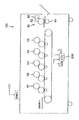
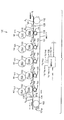
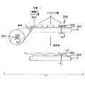
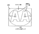
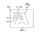
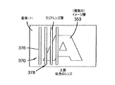
(a) 4色のイメージング後、第5ステーションが、高ガラス転移温度(Tg)の透明トナー-たとえば化学的に調製された乾式インク-を用いて、レンティキュラー材料が後続の経路で次(自己位置合わせ)に進むことのできる対抗するチャネルを形成する。たとえば高さ20-40μmの1Dリッジには約6画素分(〜258μm)の間隔が設けられて良い。そのリッジはある程度の幅(約2画素分の幅-86μm〜100μm)を有する。一の特別な実施例では、20-40μmの化学的に調製された乾式インク(CDI)が、非接触溶融(放射/閃光等)と併用されることで、リッジを形成して良い。CPDは、イーストマンコダックに譲渡された特許文献1及び特許文献2に記載されている。
(b) 逐次多重経路では、Tgが十分低いCDI材料を重ね合わせることが可能である(たとえば100-150μmで、グレイレベルイメージングでレンズ材料を形成しても良い)。低い溶融温度を用いたフュージングのときには、リッジ材料は溶融しない。そのためたとえ低Tg材料が下の有色像と位置合わせされない場合でも、溝の線が存在し、溶融した低Tg CDIが濡れることで、低Tg材料は濡れることと重力によって溝へ流れ込み、かつ下の溝に対して位置合わせされた3Dドーム形状のレンズを形成することでレンティキュラーレンズを形成する。一の特別な実施例では、5つのステーション全てがリッジ材料よりも低いTgのCDIを用いる。
ここでR1=光源に近いレンズ表面の曲率半径、及びR2=光源から遠いレンズ表面の曲率半径、である。
Claims (22)
- 受像体上に1つ以上の光学素子をエレクトログラフィックプリント方法であって:
a 所定サイズのマーキング粒子を有する第1層のトナーを堆積する工程;
b 前記第1層に対して所定サイズのマーキング粒子を有する第2層のトナーを堆積する工程;及び
c 必要に応じて前記工程aとbを繰り返して最終的な光学素子を形成する工程;
を有するエレクトログラフィックプリント方法。 - 前記(複数の)第2層に対して前記1層の多次元形状を位置合わせすることによって、位置合わせパターンに対して光学素子を形成する工程をさらに有する、請求項1に記載のエレクトログラフィックプリント方法。
- 所定の粒子特性がマーキング粒子の特別なサイズ分布を有する、請求項1に記載のエレクトログラフィックプリント方法。
- 前記マーキング粒子の特別なサイズ分布が5μmよりも大きな平均直径の体積を有する、請求項3に記載のエレクトログラフィックプリント方法。
- 前記粒子特性が、持続性、クラリティ、色、形状、表面粗さ、滑らかさ、カラークラリティ、及び屈折率のうちの1つ以上を有する、請求項1に記載のエレクトログラフィックプリント方法。
- 前記マーキング粒子の特別なサイズ分布が、前記第1層については6-12μmの体積平均直径、並びに第2層及び該第2層以降の層については12-30μmの体積平均直径を有する、請求項1に記載のエレクトログラフィックプリント方法。
- 前記マーキング粒子の特別なサイズ分布が、前記最終的な光学素子を与えるため、前記第1層についてはプリンタ上で得ることのできる最小の第1体積平均直径、及び、前記第2層の形状については前記第1体積平均直径よりも大きな体積平均直径を有する、請求項1に記載のエレクトログラフィックプリント方法。
- 前記所定サイズのマーキング粒子が12-30μmの体積平均直径を有する、請求項1に記載のエレクトログラフィックプリント方法。
- 前記最終的な光学素子が、全体として少なくとも20μmのマーキング粒子積層体の高さを有する、請求項1に記載のエレクトログラフィックプリント方法。
- 前記第1トナー層と前記第2トナー層との間に中間層をさらに有する、請求項1に記載のエレクトログラフィックプリント方法。
- 前記最終的な光学素子が周期パターンを有する、請求項1に記載のエレクトログラフィックプリント方法。
- 前記最終的な光学素子が、所定の屈折率を有する楕円形又は円形の特性のうちの1つを有する、請求項1に記載のエレクトログラフィックプリント方法。
- 前記最終的な光学素子を処理して前記最終的な光学素子に追加的な特性を与える工程をさらに有する、請求項1に記載のエレクトログラフィックプリント方法。
- 受像体上にトナー像を生成する静電グラフィックプリント装置であって:
イメージング部材;
所定サイズのマーキング粒子を用いて2層以上のトナー層を堆積することで光学素子を形成する現像ステーション;
第1層の多次元形状を第2層の多次元形状に対して位置合わせすることで最終的な光学素子を形成する位置合わせ装置;
各層の堆積を制御して前記最終的な光学素子を形成する制御装置;及び
前記最終的な光学素子を処理して前記最終的な光学素子に追加的な特性を与える処理装置;
を有する装置。 - 前記所定サイズのマーキング粒子がマーキング粒子の特別なサイズ分布を有する、請求項14に記載の装置。
- 前記最終的な光学素子が、固有の高さ、曲率半径を含む固有のプロファイル、固有の屈折率を有する、請求項14に記載の装置。
- 所定の粒子特性が、トナーの粘性、色、密度、表面張力、ガラス転移温度(Tg)、又は融点を有する、請求項14に記載の装置。
- 最終的な光学素子を表す受像体上のプリントであって:
所望のプリント像を供する前記受像体上のマーキング粒子の被覆;及び
触感があり、少なくとも20μmの積層体高さの隆起した情報が望ましい前記前記受像体上の領域でのマーキング粒子の被覆;
を有するプリント。 - 前記最終的な光学素子が当該プリントの前面に位置し、かつ前記プリント像の少なくとも一部を表す、請求項18に記載のプリント。
- 前記最終的な光学素子が当該プリントの背面に位置し、かつ前記受像体の表面特性を表す、請求項18に記載のプリント。
- 前記最終的な光学素子が当該プリントの前面及び背面に位置する、請求項18に記載のプリント。
- 受像体上でのエレクトログラフィックプリント方法であって:
a 5μmよりも大きなサイズを有する所定サイズのマーキング粒子を用いることによって、位置合わせパターンの参照印に対して第1層のトナーを堆積する工程;
b 所定の粒子特性を有する所定サイズのマーキング粒子を用いることによって、前記位置合わせパターンの参照印に対して第2層のトナーを堆積する工程;
c 前記第2層の多次元形状に対して前記第1層の多次元形状を位置合わせすることによって前記位置合わせパターンに対して最終的な多次元形状を生成する工程;及び
d 必要に応じてa、b、及びcを繰り返す工程;
を有するエレクトログラフィックプリント方法。
Applications Claiming Priority (2)
| Application Number | Priority Date | Filing Date | Title |
|---|---|---|---|
| US11/777,360 US7831178B2 (en) | 2007-07-13 | 2007-07-13 | Printing of optical elements by electrography |
| PCT/US2008/008374 WO2009011773A2 (en) | 2007-07-13 | 2008-07-08 | Printing of optical elements by electrography |
Publications (2)
| Publication Number | Publication Date |
|---|---|
| JP2010533314A true JP2010533314A (ja) | 2010-10-21 |
| JP2010533314A5 JP2010533314A5 (ja) | 2012-08-30 |
Family
ID=39893814
Family Applications (1)
| Application Number | Title | Priority Date | Filing Date |
|---|---|---|---|
| JP2010516040A Pending JP2010533314A (ja) | 2007-07-13 | 2008-07-08 | エレクトログラフィによる光学素子の印刷 |
Country Status (4)
| Country | Link |
|---|---|
| US (1) | US7831178B2 (ja) |
| EP (1) | EP2168014A2 (ja) |
| JP (1) | JP2010533314A (ja) |
| WO (1) | WO2009011773A2 (ja) |
Cited By (1)
| Publication number | Priority date | Publication date | Assignee | Title |
|---|---|---|---|---|
| JP2012083752A (ja) * | 2010-10-06 | 2012-04-26 | Xerox Corp | レンチキュラー印刷用の印刷微小凸レンズ |
Families Citing this family (25)
| Publication number | Priority date | Publication date | Assignee | Title |
|---|---|---|---|---|
| US7616917B2 (en) | 2007-11-29 | 2009-11-10 | Eastman Kodak Company | Multiple-channeled layer printing by electrography |
| DE102009008997B4 (de) * | 2009-02-14 | 2011-04-07 | Ursula Blessing | Vorrichtung zur Lenkung von Lichtstrahlen |
| US8099024B2 (en) * | 2009-03-13 | 2012-01-17 | Eastman Kodak Company | Systems and methods of producing gradient index optics by sequential printing of toners having different indices of refraction |
| JP2011002625A (ja) * | 2009-06-18 | 2011-01-06 | Konica Minolta Business Technologies Inc | 画像形成方法 |
| US20110069394A1 (en) | 2009-09-22 | 2011-03-24 | Stelter Eric C | Lens array image |
| US8778589B2 (en) * | 2009-09-30 | 2014-07-15 | Eastman Kodak Company | Digital manufacture of an optical waveguide |
| US8507037B2 (en) | 2009-10-29 | 2013-08-13 | Eastman Kodak Company | Digital manufacture of an gas or liquid separation device |
| US8145114B2 (en) | 2009-10-29 | 2012-03-27 | Eastman Kodak Company | Digital manufacture of a microfluidic device |
| JP5526822B2 (ja) * | 2010-02-01 | 2014-06-18 | 富士ゼロックス株式会社 | 静電潜像現像用トナー、静電潜像現像剤、トナーカートリッジ、プロセスカートリッジ及び画像形成装置 |
| US8383315B2 (en) * | 2010-02-18 | 2013-02-26 | Eastman Kodak Company | Raised letter printing using large yellow toner particles |
| US8652743B2 (en) * | 2010-02-18 | 2014-02-18 | Eastman Kodak Company | Raised printing using small toner particles |
| US20110200360A1 (en) * | 2010-02-18 | 2011-08-18 | Dinesh Tyagi | System to print raised printing using small toner particles |
| US8538285B2 (en) * | 2010-04-28 | 2013-09-17 | Eastman Kodak Company | Printer and fusing system |
| US8611774B2 (en) * | 2010-04-28 | 2013-12-17 | Eastman Kodak Company | Printing and fusing toner extended toner piles |
| EP2636534B1 (en) | 2010-06-07 | 2015-04-29 | LUXeXcel Holding B.V. | Method for printing optical structures |
| US8478144B2 (en) | 2010-07-29 | 2013-07-02 | Eastman Kodak Company | Method for forming a combination print with continuous imaging |
| US8180232B2 (en) | 2010-07-29 | 2012-05-15 | Eastman Kodak Company | Apparatus for making combination prints with pleasing appearance |
| US8509635B2 (en) | 2010-07-29 | 2013-08-13 | Eastman Kodak Company | Method for forming durable combination prints |
| US8548372B2 (en) * | 2010-07-29 | 2013-10-01 | Eastman Kodak Company | Method for making combination prints with pleasing appearance |
| US8467601B2 (en) * | 2010-09-15 | 2013-06-18 | Kyran Daisy | Systems, methods, and media for creating multiple layers from an image |
| US8447204B2 (en) * | 2010-10-27 | 2013-05-21 | Xerox Corporation | Simulated paper texture using clear toner on uniform substrate |
| EP2474404B1 (en) * | 2011-01-06 | 2014-12-03 | LUXeXcel Holding B.V. | Print head, upgrade kit for a conventional inkjet printer, printer and method for printing optical structures |
| JP5729293B2 (ja) * | 2011-12-26 | 2015-06-03 | カシオ計算機株式会社 | 立体画像形成方法及び立体画像形成装置 |
| US8849135B2 (en) | 2012-10-30 | 2014-09-30 | Eastman Kodak Company | Producing raised print using three toners |
| US9213255B1 (en) | 2014-08-27 | 2015-12-15 | Eastman Kodak Company | Printing tactile images with improved image quality |
Citations (2)
| Publication number | Priority date | Publication date | Assignee | Title |
|---|---|---|---|---|
| JPH0572410A (ja) * | 1991-09-18 | 1993-03-26 | Toppan Printing Co Ltd | 電子写真方式による光学部品の製造装置 |
| DE102005010506A1 (de) * | 2005-03-08 | 2006-09-21 | Schott Ag | Optisches Element und Verfahren zu dessen Herstellung |
Family Cites Families (40)
| Publication number | Priority date | Publication date | Assignee | Title |
|---|---|---|---|---|
| GB774043A (en) | 1954-05-05 | 1957-05-01 | Bendix Aviat Corp | Sonic transducer with mechanical motion transformer |
| US2955035A (en) | 1956-01-03 | 1960-10-04 | Haloid Xerox Inc | Raised xerographic images |
| US3121009A (en) | 1960-03-16 | 1964-02-11 | Rca Corp | Preparation of etched plates |
| BE607748A (ja) | 1960-09-02 | |||
| US3589290A (en) | 1966-05-20 | 1971-06-29 | Xerox Corp | Relief imaging plates made by repetitive xerographic processes |
| DE2921011C2 (de) | 1979-05-23 | 1981-04-23 | Matsumoto Yushi-Seiyaku Co., Ltd., Yao, Osaka | Verfahren zum Erzeugen eines Reliefs |
| US4694185A (en) | 1986-04-18 | 1987-09-15 | Eastman Kodak Company | Light sensing devices with lenticular pixels |
| US4833060A (en) | 1988-03-21 | 1989-05-23 | Eastman Kodak Company | Polymeric powders having a predetermined and controlled size and size distribution |
| US4965131A (en) | 1988-03-21 | 1990-10-23 | Eastman Kodak Company | Colloidally stabilized suspension process |
| EP0376322A3 (en) | 1988-12-29 | 1991-07-17 | Minolta Camera Kabushiki Kaisha | Three-dimensional image forming method |
| JPH04333858A (ja) | 1991-05-09 | 1992-11-20 | Eastman Kodak Japan Kk | 点字印刷物作成装置 |
| US5583694A (en) | 1992-07-14 | 1996-12-10 | Nippon Telegraph And Telephone Corporation | Optical element and optical axis displacement device using the same |
| US5715383A (en) | 1992-09-28 | 1998-02-03 | Eastman Kodak Company | Compound depth image display system |
| US5563694A (en) | 1993-01-15 | 1996-10-08 | Canon Kabushiki Kaisha | Printer apparatus for forming an embossed image |
| US5543964A (en) | 1993-12-28 | 1996-08-06 | Eastman Kodak Company | Depth image apparatus and method with angularly changing display information |
| US5498444A (en) | 1994-02-28 | 1996-03-12 | Microfab Technologies, Inc. | Method for producing micro-optical components |
| JPH0863039A (ja) | 1994-08-19 | 1996-03-08 | Ricoh Co Ltd | カラー画像形成装置 |
| US5745152A (en) | 1994-10-31 | 1998-04-28 | Hewlett Packard Company | Multiple beam laser scanner using lasers with different aperture sizes |
| US5583629A (en) * | 1995-06-29 | 1996-12-10 | Xerox Corporation | Color electrophotographic printing machine |
| JPH10224581A (ja) | 1997-02-03 | 1998-08-21 | Oki Data:Kk | 三次元像形成方法及び三次元像形成装置 |
| GB9800668D0 (en) | 1998-01-13 | 1998-03-11 | Nashua Corp | Enhanced microlens screens |
| JP3591334B2 (ja) | 1998-10-26 | 2004-11-17 | 富士ゼロックス株式会社 | 画像形成用トナー、その作製方法、およびそれを用いた立体画像の形成方法ならびに画像形成装置 |
| US6521905B1 (en) | 1999-09-22 | 2003-02-18 | Nexpress Solutions Llc | Method and device for detecting the position of a transparent moving conveyor belt |
| US6591747B2 (en) | 2000-05-17 | 2003-07-15 | Nexpress Solutions Llc | Method and apparatus for correcting register faults in a printing machine |
| US6421522B2 (en) | 2000-05-17 | 2002-07-16 | Nexpress Solutions Llc | Method and apparatus for setting registration in a multicolor printing machine based on a change in toner profile |
| DE10023940B4 (de) | 2000-05-17 | 2008-07-17 | Eastman Kodak Co. | Vorrichtung zum Ausrichten bogenförmigen Materials während des Transports |
| US6795250B2 (en) | 2000-12-29 | 2004-09-21 | Lenticlear Lenticular Lens, Inc. | Lenticular lens array |
| JP2002278370A (ja) | 2001-03-16 | 2002-09-27 | Fuji Xerox Co Ltd | 画像形成装置 |
| US6734449B2 (en) | 2001-11-20 | 2004-05-11 | Nexpress Solutions Llc | Device for detecting the location of an edge of a transparent material, web edge control and printing press |
| JP2004074422A (ja) | 2002-08-09 | 2004-03-11 | Mitsubishi Pencil Co Ltd | 転写箔 |
| JP4345274B2 (ja) | 2002-08-19 | 2009-10-14 | 富士ゼロックス株式会社 | 画像形成装置 |
| JP2004077931A (ja) * | 2002-08-20 | 2004-03-11 | Fuji Xerox Co Ltd | 画像形成装置 |
| JP4228621B2 (ja) | 2002-08-20 | 2009-02-25 | 富士ゼロックス株式会社 | 画像形成装置、及び画像処理装置 |
| JP4269644B2 (ja) | 2002-10-29 | 2009-05-27 | 富士ゼロックス株式会社 | 画像形成装置 |
| US7139521B2 (en) | 2003-12-23 | 2006-11-21 | Eastman Kodak Company | Gloss and differential gloss control methodology |
| GB0412961D0 (en) | 2004-06-10 | 2004-07-14 | Inovink Ltd | Improvements in and relating to printing techniques |
| US7502582B2 (en) | 2004-12-22 | 2009-03-10 | Eastman Kodak Company | Method and apparatus for printing using a tandem electrostatographic printer |
| DE102004062922A1 (de) | 2004-12-28 | 2006-07-06 | Austria Card Plastikkarten Und Ausweissysteme Gmbh | Datenträger mit taktilem Merkmal, Herstellverfahren und Anwendung |
| US7468820B2 (en) | 2005-02-22 | 2008-12-23 | Eastman Kodak Company | Profile creation for texture simulation with clear toner |
| US8358957B2 (en) | 2006-12-27 | 2013-01-22 | Eastman Kodak Company | Selective printing of raised information by electrography |
-
2007
- 2007-07-13 US US11/777,360 patent/US7831178B2/en not_active Expired - Fee Related
-
2008
- 2008-07-08 WO PCT/US2008/008374 patent/WO2009011773A2/en active Application Filing
- 2008-07-08 EP EP08780027A patent/EP2168014A2/en not_active Withdrawn
- 2008-07-08 JP JP2010516040A patent/JP2010533314A/ja active Pending
Patent Citations (2)
| Publication number | Priority date | Publication date | Assignee | Title |
|---|---|---|---|---|
| JPH0572410A (ja) * | 1991-09-18 | 1993-03-26 | Toppan Printing Co Ltd | 電子写真方式による光学部品の製造装置 |
| DE102005010506A1 (de) * | 2005-03-08 | 2006-09-21 | Schott Ag | Optisches Element und Verfahren zu dessen Herstellung |
Cited By (1)
| Publication number | Priority date | Publication date | Assignee | Title |
|---|---|---|---|---|
| JP2012083752A (ja) * | 2010-10-06 | 2012-04-26 | Xerox Corp | レンチキュラー印刷用の印刷微小凸レンズ |
Also Published As
| Publication number | Publication date |
|---|---|
| WO2009011773A3 (en) | 2009-03-12 |
| US7831178B2 (en) | 2010-11-09 |
| US20090016757A1 (en) | 2009-01-15 |
| EP2168014A2 (en) | 2010-03-31 |
| WO2009011773A2 (en) | 2009-01-22 |
Similar Documents
| Publication | Publication Date | Title |
|---|---|---|
| JP2010533314A (ja) | エレクトログラフィによる光学素子の印刷 | |
| US7965961B2 (en) | Printing of raised multidmensional toner by electography | |
| US8358957B2 (en) | Selective printing of raised information by electrography | |
| US8064788B2 (en) | Selective printing of raised information using electrography | |
| US20140004462A1 (en) | Making article with desired profile | |
| US8301062B2 (en) | Electrophotographically produced barrier images | |
| US7616917B2 (en) | Multiple-channeled layer printing by electrography | |
| US20150093553A1 (en) | Transparency document having white toner | |
| US20150093701A1 (en) | Method for creating a transparency having white toner | |
| US20140119752A1 (en) | Producing raised print using light toner | |
| US8099024B2 (en) | Systems and methods of producing gradient index optics by sequential printing of toners having different indices of refraction | |
| WO2014070533A1 (en) | Producing raised print using yellow toner | |
| WO2011102971A1 (en) | A system to print raised printing using small toner particles | |
| US20110052234A1 (en) | Enhanced fusing of raised toner using electrography | |
| US8774679B2 (en) | Electrographic tactile image printing system | |
| US8180267B2 (en) | Electrophotographically produced barrier images using an intermediate transfer member | |
| JP2010529501A (ja) | フラッドコーティングシステムのための分割ローラ | |
| US8849159B2 (en) | Electrographic printing of tactile images | |
| US8849135B2 (en) | Producing raised print using three toners | |
| US8190042B1 (en) | Electrophotographic printing apparatus | |
| JP2009109794A (ja) | 画像形成方法および画像形成装置 |
Legal Events
| Date | Code | Title | Description |
|---|---|---|---|
| A521 | Written amendment |
Free format text: JAPANESE INTERMEDIATE CODE: A523 Effective date: 20110706 |
|
| A621 | Written request for application examination |
Free format text: JAPANESE INTERMEDIATE CODE: A621 Effective date: 20110706 |
|
| A521 | Written amendment |
Free format text: JAPANESE INTERMEDIATE CODE: A523 Effective date: 20120703 |
|
| A131 | Notification of reasons for refusal |
Free format text: JAPANESE INTERMEDIATE CODE: A131 Effective date: 20120828 |
|
| A601 | Written request for extension of time |
Free format text: JAPANESE INTERMEDIATE CODE: A601 Effective date: 20121127 |
|
| A602 | Written permission of extension of time |
Free format text: JAPANESE INTERMEDIATE CODE: A602 Effective date: 20121204 |
|
| A521 | Written amendment |
Free format text: JAPANESE INTERMEDIATE CODE: A523 Effective date: 20121228 |
|
| A131 | Notification of reasons for refusal |
Free format text: JAPANESE INTERMEDIATE CODE: A131 Effective date: 20130903 |
|
| A02 | Decision of refusal |
Free format text: JAPANESE INTERMEDIATE CODE: A02 Effective date: 20140325 |