JP2010507261A - Method for patterning a material on a polymer substrate - Google Patents
Method for patterning a material on a polymer substrate Download PDFInfo
- Publication number
- JP2010507261A JP2010507261A JP2009533464A JP2009533464A JP2010507261A JP 2010507261 A JP2010507261 A JP 2010507261A JP 2009533464 A JP2009533464 A JP 2009533464A JP 2009533464 A JP2009533464 A JP 2009533464A JP 2010507261 A JP2010507261 A JP 2010507261A
- Authority
- JP
- Japan
- Prior art keywords
- polymer film
- film substrate
- functionalized
- substrate
- polymer
- Prior art date
- Legal status (The legal status is an assumption and is not a legal conclusion. Google has not performed a legal analysis and makes no representation as to the accuracy of the status listed.)
- Granted
Links
Images


Classifications
-
- H—ELECTRICITY
- H05—ELECTRIC TECHNIQUES NOT OTHERWISE PROVIDED FOR
- H05K—PRINTED CIRCUITS; CASINGS OR CONSTRUCTIONAL DETAILS OF ELECTRIC APPARATUS; MANUFACTURE OF ASSEMBLAGES OF ELECTRICAL COMPONENTS
- H05K3/00—Apparatus or processes for manufacturing printed circuits
- H05K3/02—Apparatus or processes for manufacturing printed circuits in which the conductive material is applied to the surface of the insulating support and is thereafter removed from such areas of the surface which are not intended for current conducting or shielding
- H05K3/06—Apparatus or processes for manufacturing printed circuits in which the conductive material is applied to the surface of the insulating support and is thereafter removed from such areas of the surface which are not intended for current conducting or shielding the conductive material being removed chemically or electrolytically, e.g. by photo-etch process
- H05K3/061—Etching masks
-
- C—CHEMISTRY; METALLURGY
- C23—COATING METALLIC MATERIAL; COATING MATERIAL WITH METALLIC MATERIAL; CHEMICAL SURFACE TREATMENT; DIFFUSION TREATMENT OF METALLIC MATERIAL; COATING BY VACUUM EVAPORATION, BY SPUTTERING, BY ION IMPLANTATION OR BY CHEMICAL VAPOUR DEPOSITION, IN GENERAL; INHIBITING CORROSION OF METALLIC MATERIAL OR INCRUSTATION IN GENERAL
- C23F—NON-MECHANICAL REMOVAL OF METALLIC MATERIAL FROM SURFACE; INHIBITING CORROSION OF METALLIC MATERIAL OR INCRUSTATION IN GENERAL; MULTI-STEP PROCESSES FOR SURFACE TREATMENT OF METALLIC MATERIAL INVOLVING AT LEAST ONE PROCESS PROVIDED FOR IN CLASS C23 AND AT LEAST ONE PROCESS COVERED BY SUBCLASS C21D OR C22F OR CLASS C25
- C23F1/00—Etching metallic material by chemical means
- C23F1/02—Local etching
-
- C—CHEMISTRY; METALLURGY
- C23—COATING METALLIC MATERIAL; COATING MATERIAL WITH METALLIC MATERIAL; CHEMICAL SURFACE TREATMENT; DIFFUSION TREATMENT OF METALLIC MATERIAL; COATING BY VACUUM EVAPORATION, BY SPUTTERING, BY ION IMPLANTATION OR BY CHEMICAL VAPOUR DEPOSITION, IN GENERAL; INHIBITING CORROSION OF METALLIC MATERIAL OR INCRUSTATION IN GENERAL
- C23F—NON-MECHANICAL REMOVAL OF METALLIC MATERIAL FROM SURFACE; INHIBITING CORROSION OF METALLIC MATERIAL OR INCRUSTATION IN GENERAL; MULTI-STEP PROCESSES FOR SURFACE TREATMENT OF METALLIC MATERIAL INVOLVING AT LEAST ONE PROCESS PROVIDED FOR IN CLASS C23 AND AT LEAST ONE PROCESS COVERED BY SUBCLASS C21D OR C22F OR CLASS C25
- C23F1/00—Etching metallic material by chemical means
- C23F1/10—Etching compositions
- C23F1/14—Aqueous compositions
-
- H—ELECTRICITY
- H05—ELECTRIC TECHNIQUES NOT OTHERWISE PROVIDED FOR
- H05B—ELECTRIC HEATING; ELECTRIC LIGHT SOURCES NOT OTHERWISE PROVIDED FOR; CIRCUIT ARRANGEMENTS FOR ELECTRIC LIGHT SOURCES, IN GENERAL
- H05B3/00—Ohmic-resistance heating
- H05B3/84—Heating arrangements specially adapted for transparent or reflecting areas, e.g. for demisting or de-icing windows, mirrors or vehicle windshields
-
- H—ELECTRICITY
- H05—ELECTRIC TECHNIQUES NOT OTHERWISE PROVIDED FOR
- H05K—PRINTED CIRCUITS; CASINGS OR CONSTRUCTIONAL DETAILS OF ELECTRIC APPARATUS; MANUFACTURE OF ASSEMBLAGES OF ELECTRICAL COMPONENTS
- H05K3/00—Apparatus or processes for manufacturing printed circuits
- H05K3/0073—Masks not provided for in groups H05K3/02 - H05K3/46, e.g. for photomechanical production of patterned surfaces
- H05K3/0079—Masks not provided for in groups H05K3/02 - H05K3/46, e.g. for photomechanical production of patterned surfaces characterised by the method of application or removal of the mask
-
- H—ELECTRICITY
- H05—ELECTRIC TECHNIQUES NOT OTHERWISE PROVIDED FOR
- H05K—PRINTED CIRCUITS; CASINGS OR CONSTRUCTIONAL DETAILS OF ELECTRIC APPARATUS; MANUFACTURE OF ASSEMBLAGES OF ELECTRICAL COMPONENTS
- H05K9/00—Screening of apparatus or components against electric or magnetic fields
- H05K9/0073—Shielding materials
- H05K9/0094—Shielding materials being light-transmitting, e.g. transparent, translucent
- H05K9/0096—Shielding materials being light-transmitting, e.g. transparent, translucent for television displays, e.g. plasma display panel
-
- H—ELECTRICITY
- H05—ELECTRIC TECHNIQUES NOT OTHERWISE PROVIDED FOR
- H05B—ELECTRIC HEATING; ELECTRIC LIGHT SOURCES NOT OTHERWISE PROVIDED FOR; CIRCUIT ARRANGEMENTS FOR ELECTRIC LIGHT SOURCES, IN GENERAL
- H05B2203/00—Aspects relating to Ohmic resistive heating covered by group H05B3/00
- H05B2203/017—Manufacturing methods or apparatus for heaters
-
- H—ELECTRICITY
- H05—ELECTRIC TECHNIQUES NOT OTHERWISE PROVIDED FOR
- H05K—PRINTED CIRCUITS; CASINGS OR CONSTRUCTIONAL DETAILS OF ELECTRIC APPARATUS; MANUFACTURE OF ASSEMBLAGES OF ELECTRICAL COMPONENTS
- H05K1/00—Printed circuits
- H05K1/02—Details
- H05K1/03—Use of materials for the substrate
- H05K1/0393—Flexible materials
-
- H—ELECTRICITY
- H05—ELECTRIC TECHNIQUES NOT OTHERWISE PROVIDED FOR
- H05K—PRINTED CIRCUITS; CASINGS OR CONSTRUCTIONAL DETAILS OF ELECTRIC APPARATUS; MANUFACTURE OF ASSEMBLAGES OF ELECTRICAL COMPONENTS
- H05K2201/00—Indexing scheme relating to printed circuits covered by H05K1/00
- H05K2201/09—Shape and layout
- H05K2201/09009—Substrate related
- H05K2201/09036—Recesses or grooves in insulating substrate
-
- H—ELECTRICITY
- H05—ELECTRIC TECHNIQUES NOT OTHERWISE PROVIDED FOR
- H05K—PRINTED CIRCUITS; CASINGS OR CONSTRUCTIONAL DETAILS OF ELECTRIC APPARATUS; MANUFACTURE OF ASSEMBLAGES OF ELECTRICAL COMPONENTS
- H05K2201/00—Indexing scheme relating to printed circuits covered by H05K1/00
- H05K2201/09—Shape and layout
- H05K2201/09009—Substrate related
- H05K2201/09045—Locally raised area or protrusion of insulating substrate
-
- H—ELECTRICITY
- H05—ELECTRIC TECHNIQUES NOT OTHERWISE PROVIDED FOR
- H05K—PRINTED CIRCUITS; CASINGS OR CONSTRUCTIONAL DETAILS OF ELECTRIC APPARATUS; MANUFACTURE OF ASSEMBLAGES OF ELECTRICAL COMPONENTS
- H05K2203/00—Indexing scheme relating to apparatus or processes for manufacturing printed circuits covered by H05K3/00
- H05K2203/01—Tools for processing; Objects used during processing
- H05K2203/0104—Tools for processing; Objects used during processing for patterning or coating
- H05K2203/0108—Male die used for patterning, punching or transferring
-
- H—ELECTRICITY
- H05—ELECTRIC TECHNIQUES NOT OTHERWISE PROVIDED FOR
- H05K—PRINTED CIRCUITS; CASINGS OR CONSTRUCTIONAL DETAILS OF ELECTRIC APPARATUS; MANUFACTURE OF ASSEMBLAGES OF ELECTRICAL COMPONENTS
- H05K2203/00—Indexing scheme relating to apparatus or processes for manufacturing printed circuits covered by H05K3/00
- H05K2203/05—Patterning and lithography; Masks; Details of resist
- H05K2203/0502—Patterning and lithography
- H05K2203/0528—Patterning during transfer, i.e. without preformed pattern, e.g. by using a die, a programmed tool or a laser
-
- H—ELECTRICITY
- H05—ELECTRIC TECHNIQUES NOT OTHERWISE PROVIDED FOR
- H05K—PRINTED CIRCUITS; CASINGS OR CONSTRUCTIONAL DETAILS OF ELECTRIC APPARATUS; MANUFACTURE OF ASSEMBLAGES OF ELECTRICAL COMPONENTS
- H05K2203/00—Indexing scheme relating to apparatus or processes for manufacturing printed circuits covered by H05K3/00
- H05K2203/05—Patterning and lithography; Masks; Details of resist
- H05K2203/0502—Patterning and lithography
- H05K2203/0537—Transfer of pre-fabricated insulating pattern
-
- H—ELECTRICITY
- H05—ELECTRIC TECHNIQUES NOT OTHERWISE PROVIDED FOR
- H05K—PRINTED CIRCUITS; CASINGS OR CONSTRUCTIONAL DETAILS OF ELECTRIC APPARATUS; MANUFACTURE OF ASSEMBLAGES OF ELECTRICAL COMPONENTS
- H05K2203/00—Indexing scheme relating to apparatus or processes for manufacturing printed circuits covered by H05K3/00
- H05K2203/15—Position of the PCB during processing
- H05K2203/1545—Continuous processing, i.e. involving rolls moving a band-like or solid carrier along a continuous production path
-
- H—ELECTRICITY
- H05—ELECTRIC TECHNIQUES NOT OTHERWISE PROVIDED FOR
- H05K—PRINTED CIRCUITS; CASINGS OR CONSTRUCTIONAL DETAILS OF ELECTRIC APPARATUS; MANUFACTURE OF ASSEMBLAGES OF ELECTRICAL COMPONENTS
- H05K3/00—Apparatus or processes for manufacturing printed circuits
- H05K3/0011—Working of insulating substrates or insulating layers
- H05K3/0014—Shaping of the substrate, e.g. by moulding
-
- Y—GENERAL TAGGING OF NEW TECHNOLOGICAL DEVELOPMENTS; GENERAL TAGGING OF CROSS-SECTIONAL TECHNOLOGIES SPANNING OVER SEVERAL SECTIONS OF THE IPC; TECHNICAL SUBJECTS COVERED BY FORMER USPC CROSS-REFERENCE ART COLLECTIONS [XRACs] AND DIGESTS
- Y10—TECHNICAL SUBJECTS COVERED BY FORMER USPC
- Y10T—TECHNICAL SUBJECTS COVERED BY FORMER US CLASSIFICATION
- Y10T428/00—Stock material or miscellaneous articles
- Y10T428/24—Structurally defined web or sheet [e.g., overall dimension, etc.]
- Y10T428/24479—Structurally defined web or sheet [e.g., overall dimension, etc.] including variation in thickness
-
- Y—GENERAL TAGGING OF NEW TECHNOLOGICAL DEVELOPMENTS; GENERAL TAGGING OF CROSS-SECTIONAL TECHNOLOGIES SPANNING OVER SEVERAL SECTIONS OF THE IPC; TECHNICAL SUBJECTS COVERED BY FORMER USPC CROSS-REFERENCE ART COLLECTIONS [XRACs] AND DIGESTS
- Y10—TECHNICAL SUBJECTS COVERED BY FORMER USPC
- Y10T—TECHNICAL SUBJECTS COVERED BY FORMER US CLASSIFICATION
- Y10T428/00—Stock material or miscellaneous articles
- Y10T428/26—Web or sheet containing structurally defined element or component, the element or component having a specified physical dimension
- Y10T428/268—Monolayer with structurally defined element
Abstract
ポリマー基材(105)上で第1物質(110)をパターニングする方法が記載されている。この方法は、凹部領域(108)と、隣接する隆起領域(106)と、を含むレリーフパターンの付いた主要表面(104)を有する、ポリマーフィルム基材(105)を提供する工程と、前記ポリマーフィルム基材(105)の前記主要表面(104)上に第1物質(110)を堆積させて、コーティングされたポリマーフィルム基材を形成する工程と、前記コーティングされたポリマーフィルム基材の前記隆起領域(106)の上に機能化材料の層(131)を選択的に形成して、機能化された隆起領域と機能化されていない凹部領域とを形成する工程と、前記ポリマー基材の、機能化されていない凹部領域から前記第1物質(110)を選択的にエッチングする工程と、を含む。 A method for patterning a first material (110) on a polymer substrate (105) is described. The method comprises providing a polymer film substrate (105) having a major surface (104) with a relief pattern comprising a recessed region (108) and an adjacent raised region (106); Depositing a first material (110) on the major surface (104) of the film substrate (105) to form a coated polymer film substrate; and the ridges of the coated polymer film substrate. Selectively forming a layer (131) of functionalized material over the region (106) to form a functionalized raised region and a non-functionalized recessed region; and Selectively etching the first material (110) from a non-functionalized recessed area.
Description
本開示内容は、一般に、ポリマー基材上で物質をパターニングする方法、及びかかる方法によって形成される物品に関する。 The present disclosure generally relates to a method of patterning a material on a polymer substrate and an article formed by such a method.
金属物質のパターンを有するポリマーフィルムは、多種多様な商業的用途を有している。場合によっては、導電性グリッドは、肉眼では視認できないほど十分に細かいこと、及び透明なポリマー基材上に担持されていることが望ましい。透明な導電性シートには様々な用途があり、例えば、抵抗加熱ウィンドウ、電磁波(EMI)シールド層、静電気消散構成要素、アンテナ、コンピュータディスプレイ用のタッチスクリーン、並びにエレクトロクロミックウィンドウ用、光起電デバイス用、エレクトロルミネッセント素子用、及び液晶ディスプレイ用の表面電極が挙げられる。 Polymer films having a pattern of metallic material have a wide variety of commercial uses. In some cases, it is desirable for the conductive grid to be sufficiently fine that it cannot be viewed with the naked eye and to be supported on a transparent polymer substrate. Transparent conductive sheets have a variety of uses, such as resistive heating windows, electromagnetic wave (EMI) shielding layers, electrostatic dissipation components, antennas, touch screens for computer displays, and electrochromic windows, photovoltaic devices And surface electrodes for electroluminescent devices and liquid crystal displays.
EMIシールドとしての用途に本質的に透明な導電性グリッドを使用することが知られている。グリッドは、透明シートの間に挟まれた又は積層されたか、あるいは基材に埋め込まれた金属ワイヤのネットワーク又はスクリーンから形成することができる(米国特許第3,952,152号、米国特許第4,179,797号、米国特許第4,321,296号、米国特許第4,381,421号、米国特許第4,412,255号)。ワイヤスクリーンを利用することの一つの欠点は、非常に細いワイヤが取り扱い難いこと、又は極めて細かなワイヤスクリーンの作製及び取り扱いが困難であることである。例えば、直径20マイクロメートルの銅ワイヤは、引っ張り強度が0.28N(1オンス(28グラム重))しかないため、損傷し易い。直径20マイクロメートルのワイヤを用いて製造されたワイヤスクリーンは、非常に細いワイヤが取り扱い難いため、入手可能であるが高価である。 It is known to use a conductive grid that is essentially transparent for use as an EMI shield. The grid can be formed from a network or screen of metal wires sandwiched or laminated between transparent sheets or embedded in a substrate (US Pat. No. 3,952,152, US Pat. No. 4). , 179,797, US Pat. No. 4,321,296, US Pat. No. 4,381,421, US Pat. No. 4,412,255). One disadvantage of utilizing wire screens is that very thin wires are difficult to handle or very fine wire screens are difficult to make and handle. For example, a 20 micrometer diameter copper wire is susceptible to damage because it has a tensile strength of only 0.28 N (1 ounce (28 gram weight)). Wire screens made with 20 micrometer diameter wires are available but expensive because very thin wires are difficult to handle.
既存のワイヤスクリーンを基材に埋め込むのではなく、最初に溝又はチャネルのパターンを基材に形成してから溝又はチャネルに導電性物質を充填することによって導電性パターンをその場で製造することも可能である。この方法は、導電性回路のラインやパターンを様々な手段で作製するために用いられてきたが、通常は比較的目の粗い規模のライン及びパターンに使用されている。溝は、成形法やエンボス加工によって、又はリソグラフィー法によって基材に形成することができる。溝には、その後、導電性インク又はエポキシを充填するか(米国特許第5,462,624号)、蒸着金属、スパッタ金属、若しくはメッキ金属を充填するか(米国特許第3,891,514号、米国特許第4,510,347号、及び米国特許第5,595,943号)、融解金属を充填するか(米国特許第4,748,130号)、あるいは金属粉末を充填することができる(米国特許第2,963,748号、米国特許第3,075,280号、米国特許第3,800,020号、米国特許第4,614,837号、米国特許第5,061,438号、及び米国特許第5,094,811号)。ポリマーフィルム上の導電性グリッドは、導電性ペーストを印刷することによって(米国特許第5,399,879号)、又は光リソグラフィー法及びエッチングによって(米国特許第6,433,481号)作製されてきた。これら先行技術の方法には制限がある。例えば、導電性のインク又はエポキシに関する一つの問題は、導電性が、隣接する導電性粒子間の接触形成に左右されることであって、全体の導電性は通常、固体金属に比べてかなり小さい。金属の蒸着又は電気メッキは一般にスピードが遅く、多くの場合、溝の間に堆積している余剰の金属を取り除くために後続の工程を必要とする。融解金属は、溝の中に入れることができるが、通常は、金属が濡らす溝の中に、ある物質を付着させる必要がある。そうでなければ、融解金属は、融解金属の表面張力のために、溝に入り込むことも留まることもできない。 Rather than embedding an existing wire screen in a substrate, first forming a pattern of grooves or channels in the substrate and then producing the conductive pattern in situ by filling the grooves or channels with a conductive material Is also possible. This method has been used to produce conductive circuit lines and patterns by various means, but is typically used for lines and patterns on a relatively coarse scale. The grooves can be formed in the substrate by a molding method, an embossing process, or a lithography method. The groove is then filled with conductive ink or epoxy (U.S. Pat. No. 5,462,624), or deposited metal, sputtered metal, or plated metal (U.S. Pat. No. 3,891,514). US Pat. No. 4,510,347, and US Pat. No. 5,595,943), filled with molten metal (US Pat. No. 4,748,130), or filled with metal powder (US Pat. No. 2,963,748, US Pat. No. 3,075,280, US Pat. No. 3,800,020, US Pat. No. 4,614,837, US Pat. No. 5,061,438 And US Pat. No. 5,094,811). Conductive grids on polymer films have been made by printing conductive paste (US Pat. No. 5,399,879) or by photolithography and etching (US Pat. No. 6,433,481). It was. These prior art methods have limitations. For example, one problem with conductive inks or epoxies is that the conductivity depends on the contact formation between adjacent conductive particles, and the overall conductivity is usually much less than that of a solid metal. . Metal deposition or electroplating is generally slow and often requires subsequent steps to remove excess metal deposited between the grooves. Molten metal can be put into the groove, but usually a substance needs to be deposited in the groove wetted by the metal. Otherwise, the molten metal cannot enter or stay in the groove due to the surface tension of the molten metal.
導電性グリッドに加えて、導電性物質のパターンを電気回路の形態で担持するポリマーフィルムもまた有用である。フレキシブル回路は、電子的構成要素の支持や相互接続のみならず、センサーの製造にも使用される。センサーの例としては、環境センサー、医療用センサー、化学センサー、及びバイオメトリックセンサーが挙げられる。いくつかのセンサーは、好ましくは透明である。導電性グリッドの場合のように、ポリマーフィルム基材上のフレキシブル回路は多くの場合、フォトレジストの付着、露光、現像、及び除去という、複数の工程を含む光リソグラフィー法を用いて作製される。かかる高価な設備やこれほど多くの製造プロセス工程を必要としない代替の方法が、当該産業界では望まれている。 In addition to conductive grids, polymer films that carry a pattern of conductive material in the form of an electrical circuit are also useful. Flexible circuits are used not only to support and interconnect electronic components, but also to the manufacture of sensors. Examples of sensors include environmental sensors, medical sensors, chemical sensors, and biometric sensors. Some sensors are preferably transparent. As with conductive grids, flexible circuits on polymer film substrates are often made using photolithographic methods that include multiple steps of photoresist deposition, exposure, development, and removal. There is a desire in the industry for such expensive equipment and alternative methods that do not require as many manufacturing process steps.
回路は、溝の中に金属粉末を入れた後、この粉末を圧縮して粒子間の電気接触を増強することによって、作製されている。リリー(Lillie)ら(米国特許第5,061,438号)及びケイン(Kane)ら(米国特許第5,094,811号)では、この方法を利用してプリント基板を形成している。しかしながら、これらの方法は、微細な回路や微細な金属パターンの製造には実用的ではない。微細な規模では、エンボス加工されたパターンの上部に用具を再設置又は再度位置合わせして金属を圧縮することが難しい可能性がある。例えば、20マイクロメートル幅のチャネルのパターンを有するシートでは、用具をパターンの上部に、シートの片面からもう一方の面までほぼ3マイクロメートルの精度で設置する必要がある。多くの用途では、シートは30cm×30cm程度であってよい。熱可塑性シートの熱収縮に起因する寸法変化は、典型的に、形成温度から室温までの冷却中に約1パーセント以上である。すなわち、30cm×30cmのシートの場合、1パーセントの収縮によって全体で0.3cm縮小する。この値は、要求されている3マイクロメートルの設置精度よりも1000倍大きく、用具の正確な再配置を困難にする。 The circuit is made by placing a metal powder in the groove and then compressing the powder to enhance electrical contact between the particles. Lillie et al. (US Pat. No. 5,061,438) and Kane et al. (US Pat. No. 5,094,811) use this method to form printed circuit boards. However, these methods are not practical for manufacturing fine circuits and fine metal patterns. On a fine scale, it can be difficult to compress the metal by repositioning or repositioning the tool on top of the embossed pattern. For example, in a sheet having a 20 micrometer wide channel pattern, the tool needs to be placed on the top of the pattern with an accuracy of approximately 3 micrometers from one side of the sheet to the other. For many applications, the sheet may be on the order of 30 cm × 30 cm. The dimensional change due to thermal shrinkage of the thermoplastic sheet is typically about 1 percent or more during cooling from the forming temperature to room temperature. That is, in the case of a 30 cm × 30 cm sheet, the contraction of 1 percent causes a total reduction of 0.3 cm. This value is 1000 times greater than the required 3 micrometer installation accuracy, making accurate relocation of the tool difficult.
本開示は、ポリマーフィルム基材上で物質をパターニングする方法、及び構造化されたポリマーフィルム基材とパターン化された機能化材料とを含む物品に関する。特に、本開示は、本質的に形状のない印刷プレートを用いてポリマーフィルム基材の隆起部分上に機能化材料を選択的に転写した後、物質を機能化されていない領域(凹部領域又は非隆起領域)からエッチングすることによる、ポリマー基材上で物質をパターニングする方法に関する。この新たな方法は、機能化材料(単数及び複数)の微細規模のパターンを、ロールツーロール(roll-to-roll)装置の同期にほとんど関係なく、高速で連続的にウェブ基材へ転写することができる。 The present disclosure relates to a method of patterning a material on a polymer film substrate, and an article comprising a structured polymer film substrate and a patterned functionalized material. In particular, the present disclosure provides for the non-functionalized areas (recessed areas or non-functionalized areas) after selective transfer of the functionalized material onto the raised portions of the polymer film substrate using an essentially shapeless printing plate. The invention relates to a method of patterning a material on a polymer substrate by etching from a raised region. This new method transfers fine-scale patterns of functionalized material (s) to a web substrate at high speed and continuously, with little or no synchronization of roll-to-roll equipment. be able to.
ある代表的な実施において、方法には、凹部領域と、隣接する隆起領域と、を含むレリーフパターンの付いた主要表面を有する、ポリマーフィルム基材を提供する工程と、前記ポリマーフィルム基材の前記主要表面に第1物質を堆積させて、コーティングされたポリマーフィルム基材を形成する工程と、前記コーティングされたポリマーフィルム基材の前記隆起領域に機能化材料の層を選択的に形成して、機能化された隆起領域と機能化されていない凹部領域とを形成する工程と、前記ポリマーフィルム基材の、機能化されていない凹部領域から前記第1物質を選択的にエッチングする工程と、が含まれる。 In one exemplary implementation, the method includes providing a polymer film substrate having a major surface with a relief pattern that includes a recessed region and an adjacent raised region; and Depositing a first material on a major surface to form a coated polymer film substrate; and selectively forming a layer of functionalized material in the raised areas of the coated polymer film substrate; Forming a functionalized raised region and a non-functionalized recessed region; and selectively etching the first material from the nonfunctionalized recessed region of the polymer film substrate. included.
別の代表的な実施では、物品は、隆起領域と、隣接する凹部領域と、を含むレリーフ構造の付いた主要表面を有するポリマーフィルムを含み、前記隆起領域は第1物質で選択的にコーティングされており、前記第1物質は機能化分子を担持している。 In another exemplary implementation, the article includes a polymer film having a major surface with a relief structure that includes a raised area and an adjacent recessed area, the raised area being selectively coated with a first material. And the first substance carries a functionalized molecule.
本発明による方法及び物品に関する前記及び他の態様は、図面と併せて以下の「発明を実施するための形態」から、当業者には容易に明白になるであろう。 The foregoing and other aspects of the method and article according to the present invention will be readily apparent to those skilled in the art from the following Detailed Description, taken together with the drawings.
また、添付の図面と関連して本発明の様々な実施形態を記述する、以下の「発明を実施するための形態」を検討することで、本発明をより完全に理解することができる。 In addition, the present invention can be more fully understood by considering the following detailed description that describes various embodiments of the invention in connection with the accompanying drawings.
本発明は様々な修正及び代替形態に補正することができるが、本発明の詳細は、図面に例示されており、また詳述される。しかしながら、本発明を、説明される特定の実施形態に制限する意図はないと理解すべきである。反対に、その意図は、本発明の趣旨及び範囲内にある全ての修正、等価形態、及び代替物を対象とすることである。 While the invention is amenable to various modifications and alternative forms, details of the invention are illustrated in the drawings and will be described in detail. However, it should be understood that the invention is not intended to be limited to the particular embodiments described. On the contrary, the intent is to cover all modifications, equivalents, and alternatives falling within the spirit and scope of the invention.
それ故に、本発明の開示は、ポリマーフィルム基材上で物質をパターニングする方法を目的とする。ポリマーフィルム基材は、その主要表面の一方又は両方にレリーフパターン(すなわち、構造又はミクロ構造)を有している。主要表面にレリーフパターンの付いたポリマーフィルム基材は、構造化又はミクロ構造化されていると考えられる。 The present disclosure is therefore directed to a method of patterning a material on a polymer film substrate. The polymer film substrate has a relief pattern (ie, structure or microstructure) on one or both of its major surfaces. A polymer film substrate with a relief pattern on the major surface is considered to be structured or microstructured.
レリーフパターンの付いた、とは、表面にトポグラフィーパターン、例えば、凹部領域(例えば、チャネル、窪み、溝)のパターン、又は隆起領域(例えば、隆起部、柱、半球)のパターンを含むことを意味する。ポリマーフィルム基材は、例えば、成型と硬化とによるミクロ構造転写(cast-and-cure microreplication)又はエンボス加工によって構造化することができ、その後、これら構造化されたフィルム基材は、その構造化されたフィルム基材の隆起領域上に選択的に配置された機能化分子を有することができる。 With a relief pattern is meant to include a topographic pattern on the surface, for example a pattern of recessed areas (eg channels, depressions, grooves) or a pattern of raised areas (eg ridges, pillars, hemispheres). means. Polymer film substrates can be structured, for example, by cast-and-cure microreplication or embossing by molding and curing, after which these structured film substrates are structured. Can have functionalized molecules selectively placed on the raised regions of the formed film substrate.
これら機能化分子は、例えば、選択エッチングを通して、後続のパターニング用のマスクとして役立つことができる。本発明はそのように限定されるものではないが、以下に提供される実施例の考察を通じて本発明の様々な態様への理解が得られるであろう。 These functionalized molecules can serve as a mask for subsequent patterning, for example through selective etching. While the present invention is not so limited, an appreciation of various aspects of the invention will be gained through a discussion of the examples provided below.
次に定義する用語については、別の定義が特許請求の範囲中あるいは本明細書中に与えられなければ、これらの定義が適用されるものとする。 For the terms defined below, these definitions shall apply unless a different definition is given in the claims or herein.
「領域」とは、表面全体(例えば、基材表面)の、近接する分画部分を指す。隆起領域とは、主要表面の隣接領域から突出し、ある高さを有する表面領域を指す。凹部領域とは、主要表面の隣接領域に関して内側に広がり、ある深さを有する表面領域を指す。隆起領域及び/又は凹部領域は、不連続な領域であることができ、その場合、それと隣接する凹部領域及び/又は隆起領域(それぞれ)が、全ての側でその不連続な領域を取り囲んでいる。あるいは、隆起領域又は凹部領域は、表面の長さ又は幅に沿って概ね線状に延びたほぼ近接する領域であることもでき、主要表面の隣接する領域は、全ての側でそれと近接する領域を取り囲んでいるわけではない。基材の隆起表面領域は、一般に、基材表面と他の物体の平坦な表面(すなわち、構造化されていない平面的なもの)とが接触したときに、その平坦な物体の面積が隆起領域及び任意の隣接する凹部領域よりも大きい場合に、別の物体の平坦な表面に接触する基材表面の部分である。基材の凹部表面領域(単数又は複数)は一般に、このように、隆起表面領域に対して補足的な表面領域である。補足的とは、全ての隆起表面領域(単数又は複数)と全ての凹部表面領域(単数又は複数)とが、本質的に主要表面全体を画定するように組み合わさっていることを意味する。 “Region” refers to the fractional portion of the entire surface (eg, the substrate surface) that is in close proximity. A raised area refers to a surface area that protrudes from an adjacent area of the main surface and has a certain height. A recessed area refers to a surface area that extends inward and has a certain depth with respect to an adjacent area of the main surface. The raised area and / or recessed area can be a discontinuous area, in which case the adjacent recessed area and / or raised area (respectively) surround the discontinuous area on all sides. . Alternatively, the raised or recessed area can be a generally adjacent area extending generally linearly along the length or width of the surface, and the adjacent area of the major surface is the area adjacent to it on all sides Is not surrounding. The raised surface area of a substrate is generally defined as the area of the flat object when the substrate surface contacts the flat surface of another object (ie, unstructured planar). And the portion of the substrate surface that contacts the flat surface of another object when larger than any adjacent recessed area. The concave surface area (s) of the substrate is thus generally a surface area that is complementary to the raised surface area. Complementary means that all raised surface area (s) and all recessed surface area (s) are combined to essentially define the entire major surface.
機能化材料の層を「選択的に」形成するとは、機能化材料の層を一方の表面領域には形成するが、機能化材料の層を他方の表面領域には形成しないことを指す。基材表面上に選択的に堆積される機能化材料の層は、基材表面全体には堆積されていない。すなわち、機能化材料の層は、あるパターンを基材表面上に形成する。 “Selectively” forming a layer of functionalized material refers to forming a layer of functionalized material in one surface region but not forming a layer of functionalized material in the other surface region. The layer of functionalized material that is selectively deposited on the substrate surface is not deposited over the entire substrate surface. That is, the layer of functionalized material forms a pattern on the substrate surface.
ポリマー「フィルム」基材は、ロールツーロール(roll-to-roll)様式で加工するのに十分な可撓性及び強度を有する、平坦なシート状のポリマー材料である。ロールツーロール(roll-to-roll)とは、材料を支持体上に巻き取る又は支持体から巻戻すプロセスだけでなく、何らかの方法で更に加工するプロセスを意味する。更なるプロセスの例としては、コーティング、スリット加工、打ち抜き加工、及び放射線への曝露などが挙げられる。ポリマーフィルムは、一般には約5マイクロメートル〜1000マイクロメートルまでの範囲の様々な厚さで、製造することができる。多くの実施形態において、ポリマーフィルムの厚さは、約25マイクロメートル〜約500マイクロメートル、又は約50マイクロメートル〜約250マイクロメートル、又は約75マイクロメートル〜約200マイクロメートルの範囲である。一方又は両方の主要表面にレリーフ構造を含むフィルムの場合、フィルムの厚さとは、フィルムの面積全体の平均厚さを表す。 A polymeric “film” substrate is a flat sheet of polymeric material having sufficient flexibility and strength to be processed in a roll-to-roll manner. By roll-to-roll is meant the process of further processing in some way, as well as the process of winding the material on or off the support. Examples of further processes include coating, slitting, stamping, and exposure to radiation. Polymer films can be manufactured in various thicknesses, generally ranging from about 5 micrometers to 1000 micrometers. In many embodiments, the thickness of the polymer film ranges from about 25 micrometers to about 500 micrometers, or from about 50 micrometers to about 250 micrometers, or from about 75 micrometers to about 200 micrometers. In the case of a film including a relief structure on one or both major surfaces, the film thickness represents the average thickness of the entire area of the film.
金属の「選択的な」除去又はエッチングとは、一方の表面領域上の物質は除去するが、もう一方の表面領域上の物質は除去しないことを意味する。基材表面上で選択的に除去される物質は、基材表面全体からは除去されていない。 “Selective” removal or etching of metal means removing material on one surface area, but not removing material on the other surface area. Substances that are selectively removed on the substrate surface are not removed from the entire substrate surface.
「機能化分子」とは、化学結合によって基材表面(又はコーティングされた基材表面)に付着している分子を指す。機能化分子は、それが付着される表面領域を不動態化又は活性化することができる。多くの実施形態では、機能化分子は、自己組織化単層(self-assembled monolayer)を形成する。 “Functionalized molecule” refers to a molecule attached to a substrate surface (or coated substrate surface) by chemical bonding. A functionalized molecule can passivate or activate the surface region to which it is attached. In many embodiments, the functionalized molecule forms a self-assembled monolayer.
「自己組織化単層」とは、表面に(例えば、化学結合によって)付着している分子の単層であって、表面に関して及び更には互いに関しても好ましい配向をとる分子の単層を指す。自己組織化単層は、表面の特性が変わるほど完全に表面を覆うとされている。例えば、自己組織化単層を適用することで、表面エネルギーの低下をもたらすことができる。 “Self-assembled monolayer” refers to a monolayer of molecules attached to a surface (eg, by chemical bonding) and having a preferred orientation with respect to the surface and also with respect to each other. The self-assembled monolayer is said to completely cover the surface as the surface properties change. For example, applying a self-assembled monolayer can result in a reduction in surface energy.
自己組織化単層を形成するのに好適な化学種の例としては、有機硫黄化合物、シラン、ホスホン酸、ベンゾトリアゾール、及びカルボン酸などの有機化合物が挙げられる。かかる化合物の例は、ウルマン(Ulman)が総説で論じている(A.ウルマン(A. Ulman)、「自己組織化単層の形成と構造(Formation and Structure of Self-Assembled Monolayers)」、化学概論(Chem. Rev.)、96、1533〜1554(1996年))。有機化合物に加えて、特定の有機金属化合物も、自己組織化単層を形成するのに有用である。自己組織化単層を形成するのに好適な有機硫黄化合物の例としては、アルキルチオール、ジアルキルジスルフィド、ジアルキルスルフィド、アルキルキサンテート、及びジアルキルチオカルバメートが挙げられる。自己組織化単層を形成するのに好適なシランの例としては、有機クロロシラン及び有機アルコキシシランが挙げられる。自己組織化単層を形成するのに好適なホスホン酸分子の例は、パラライト(Pellerite)らが論じている(M.J.パラライト(M. J. Pellerite)、T.D.ダンバー(T. D. Dunbar)、L.D.ボードマン(L. D. Boardman)、及びE.J.ウッド(E. J. Wood)、「アルミニウム上でのアルカンホスホン酸からの自己組織化単層の形成に関するフッ素化効果:動力学及び構造(“Effects of Fluorination on Self-Assembled Monolayer Formation from Alkanephosphonic Acids on Aluminum: Kinetics and Structure”」、物理化学会誌B(Journal of Physical Chemistry B)、107、11726〜11736(2003年))。自己組織化単層を形成するのに好適な化学種としては、例えば、炭化水素化合物、部分フッ素化炭化水素化合物、又はペルフルオロ化合物を挙げることができる。自己組織化単層は、2つ以上の異なる化学種を含むことができる。2つ以上の異なる化学種を利用する際、それら化学種は、自己組織化単層中に混合物として又は相分離した形態で存在していてよい。 Examples of chemical species suitable for forming a self-assembled monolayer include organic compounds such as organic sulfur compounds, silanes, phosphonic acids, benzotriazoles, and carboxylic acids. Examples of such compounds are discussed in a review by Ulman (A. Ulman, “Formation and Structure of Self-Assembled Monolayers”, Introduction to Chemistry). (Chem. Rev.), 96, 1533-1554 (1996)). In addition to organic compounds, certain organometallic compounds are also useful for forming self-assembled monolayers. Examples of organic sulfur compounds suitable for forming a self-assembled monolayer include alkyl thiols, dialkyl disulfides, dialkyl sulfides, alkyl xanthates, and dialkylthiocarbamates. Examples of silanes suitable for forming a self-assembled monolayer include organochlorosilanes and organoalkoxysilanes. Examples of phosphonic acid molecules suitable for forming a self-assembled monolayer are discussed by Pellerite et al. (MJ Pellerite, TD Dunbar, L LD Boardman and EJ Wood, “Fluorination effects on the formation of self-assembled monolayers from alkanephosphonic acids on aluminum: kinetics and structure (“ Effects of Fluorination on Self-Assembled Monolayer Formation from Alkanephosphonic Acids on Aluminum: Kinetics and Structure ”, Journal of Physical Chemistry B (107, 11726-11736 (2003)). Suitable chemical species to do include, for example, hydrocarbon compounds, partially fluorinated hydrocarbon compounds, or perfluoro compounds. When using more than three single .2 can include different chemical species or more different chemical species, they species may be present in a mixture or as a phase-separated form self-assembled monolayer.
自己組織化単層を形成するのに有用な例示的な分子としては、例えば、(C3〜C20)アルキルチオール、又は(C10〜C20)アルキルチオール、又は(C15〜C20)アルキルチオールが挙げられる。アルキル基は、直鎖又は分枝状であることができ、自己組織化単層の形成を妨害しない置換基で置換又は非置換することが可能である。 Exemplary molecules useful for forming a self-assembled monolayer include, for example, (C 3 -C 20 ) alkyl thiols, or (C 10 -C 20 ) alkyl thiols, or (C 15 -C 20 ). An alkyl thiol is mentioned. Alkyl groups can be straight or branched and can be substituted or unsubstituted with substituents that do not interfere with the formation of the self-assembled monolayer.
自己組織化単層は、無機物質でコーティングされたポリマー表面(例えば、金属でコーティングされたポリマー表面)に様々な方法を利用して形成することができる。多くの実施形態では、自己組織化単層は、選択された領域又は隆起領域と、自己組織化単層分子がその中又はその上に配置されたプレートとを接触させることによって、金属でコーティングされたポリマー基材の隆起領域に適用される。プレートとは、機能化分子を基材に供給するエラストマー転写要素を意味する。プレートは、平面的であっても、円筒形であっても、又は別の形であってもよい。 Self-assembled monolayers can be formed using various methods on polymer surfaces coated with inorganic materials (eg, polymer surfaces coated with metal). In many embodiments, the self-assembled monolayer is coated with a metal by contacting selected regions or raised regions with a plate in which or on which the self-assembled monolayer molecules are placed. Applied to the raised region of the polymer substrate. By plate is meant an elastomeric transfer element that supplies functionalized molecules to a substrate. The plate may be planar, cylindrical or another shape.
多くの実施形態では、自己組織化単層分子が中又は上に配置されたプレート(又は円筒)には形状がなく、ポリマー基材上の自己組織化単層のパターンは、ポリマー基材の隆起領域又は凹部領域によって画定される。形状がないとは、プレートが、基材表面上のレリーフ構造で平滑である(レリーフ構造がない)ことを意味する。先行技術の方法(例えば、マイクロコンタクト印刷、米国特許第5,512,131号)と比べて、本開示内容では、基材に関するプレートのずれを規制する必要なしに、機能化分子(例えば、自己組織化単層)をポリマーフィルム表面上にパターンで配置することができる。マイクロコンタクト印刷では、パターン忠実度を保持するために、レリーフ構造の型と平坦な基材とがずれずに接触及び分離する必要がある。このことは、極めて細かな形状寸法のロールツーロール(roll-to-roll)を可撓性ポリマーフィルム基材上に連続してマイクロコンタクト印刷しようとする場合、特に困難である。ポリマーフィルム基材と、パターンの小さな形状寸法(例えば、10マイクロメートル未満、1マイクロメートル未満)とを用いて連続的にマイクロコンタクト印刷するロールツーロールの実施は、同期化(例えば、印刷プレートの回転に関するウェブ前進の制御)に重要な課題を有している。本開示は、プレートレリーフの印刷と、基材との接触や基材からの剥離の詳細とを組み合わせるのではなく、転写した機能化分子のパターンを基材のレリーフ構造で画定させることによって、この問題を克服している。また、エラストマー材料は、機能化分子(例えば、自己組織化単層)を表面へ転写するのに特に有用であるが、微細なレリーフパターンで構造化する場合は、印刷操作によって変形し易い。本発明は、ポリマーフィルム基材上の機能化分子のパターンを潜在的に更に固い物質(エラストマー印刷プレートよりもむしろ、基材自体)で画定させて、機能化分子、そして堆積した金属に関する最終的なパターン忠実度を更に確実なものにすることができる。 In many embodiments, the plate (or cylinder) with the self-assembled monolayer molecules disposed in or on it has no shape, and the pattern of the self-assembled monolayer on the polymer substrate is a ridge of the polymer substrate. Defined by a region or a recessed region. The absence of shape means that the plate is smooth with a relief structure on the substrate surface (no relief structure). Compared to prior art methods (eg, microcontact printing, US Pat. No. 5,512,131), the present disclosure provides for functionalized molecules (eg, self-adjusting) without having to regulate plate displacement relative to the substrate. Organized monolayers) can be arranged in a pattern on the polymer film surface. In microcontact printing, in order to maintain pattern fidelity, it is necessary to contact and separate the relief structure mold and the flat substrate without shifting. This is especially difficult when trying to continuously micro-contact rolls of very fine geometries on flexible polymer film substrates. The roll-to-roll implementation of continuous microcontact printing using a polymer film substrate and a small feature size of the pattern (eg, less than 10 micrometers, less than 1 micrometer) can be synchronized (eg, printing plate Control of web advancement with respect to rotation). The present disclosure does not combine the printing of the plate relief with the details of contact with the substrate and release from the substrate, but by having the transferred functional molecule pattern defined by the relief structure of the substrate. Overcoming the problem. Elastomeric materials are also particularly useful for transferring functionalized molecules (eg, self-assembled monolayers) to the surface, but are easily deformed by printing operations when structured with a fine relief pattern. The present invention allows the pattern of functionalized molecules on a polymer film substrate to be defined by a potentially harder material (the substrate itself, rather than the elastomer printing plate), and finally the functionalized molecule and the deposited metal Pattern fidelity can be further ensured.
プレートを形成するのに有用なエラストマーとしては、シリコーン、ポリウレタン、EPDMゴム、並びに現在市販されている一連のフレキソ印刷プレート材料(例えば、デラウェア州ウィルミントン(Wilmington)のE.I.デュポン・ド・ヌムール・アンド・カンパニー(E. I. du Pont de Nemours and Company)から商標名サイレル(Cyrel)(登録商標)として市販されているもの)が挙げられる。ポリジメチルシロキサン(PDMS)が特に有用である。プレートは、複合材料から製造することができる。エラストマーは、ゲル物質(例えば、共連続的な液相及び固相)、例えば、ヒドロゲルであることができる。プレートは、別の材料、例えば、使用中のプレートの形と大きさを確定するための更に固い材料の上に担持されることができる。プレートは、機能化分子の転写中に活性化する(例えば、加熱する、又は超音波で推進する)ことができる。 Elastomers useful for forming the plates include silicone, polyurethane, EPDM rubber, and a series of flexographic plate materials currently on the market (eg, EI DuPont de Dupont, Wilmington, Del.). And the trade name Cyrel (registered trademark) from EI du Pont de Nemours and Company). Polydimethylsiloxane (PDMS) is particularly useful. The plate can be manufactured from a composite material. Elastomers can be gel materials (eg, co-continuous liquid and solid phases), eg, hydrogels. The plate can be carried on another material, such as a harder material to determine the shape and size of the plate in use. The plate can be activated (eg, heated or propelled with ultrasound) during the transfer of the functionalized molecule.
有用なエッチング化学物質は、パターニングされる物質及び機能化材料に依存する。エッチング化学物質の選択基準としては、パターニングされる物質に対する十分なエッチング速度だけでなく、機能化材料との適合性も挙げられる。適合性とは、パターニングされた機能化材料が、パターンエッチング工程に有効な遮蔽マスクとして働くことを意味する。金をパターニングする場合、有用なエッチング系としては、硝酸第二鉄系及びチオ尿素系のものが挙げられる。金に有用な他のエッチング系は、フェリシアン化カリウム系である。酸化インジウムスズをパターニングするのに有用なエッチング化学物質は、シュウ酸系のものが挙げられる。銅、金、又は銀をエッチパターニングする場合、例えば、酸素及びシアン化物イオンを溶解したアルカリ性溶液が有用である。本明細書では、エッチング選択性を改善するために、エッチング槽に添加物を含めることが検討される。(米国特許第7,041,232号)。 Useful etch chemistries depend on the material to be patterned and the functionalized material. Etching chemistry selection criteria include compatibility with functionalized materials as well as sufficient etch rates for the material being patterned. By compatible is meant that the patterned functionalized material acts as an effective shielding mask for the pattern etching process. When patterning gold, useful etching systems include ferric nitrate and thiourea. Another etching system useful for gold is the potassium ferricyanide system. Etching chemicals useful for patterning indium tin oxide include oxalic acid-based ones. When etching patterning copper, gold, or silver, for example, an alkaline solution in which oxygen and cyanide ions are dissolved is useful. In the present specification, it is considered to include an additive in the etching tank in order to improve the etching selectivity. (US Pat. No. 7,041,232).
ポリマーフィルム基材上の無機物質コーティング(例えば、金属コーティング)は、自己組織化単層を担持するために用いられ、そしてその後、エッチングによりパターニングすることができる。無機コーティングには、例えば、元素金属、金属合金、金属間化合物、金属酸化物、金属硫化物、金属炭化物、金属窒化物、及びこれらの組み合わせを挙げることができる。自己組織化単層を担持するための代表的な無機表面としては、金、銀、パラジウム、白金、ロジウム、銅、ニッケル、鉄、インジウム、スズ、タンタル、並びにこれら元素の混合物、合金、及び化合物が挙げられる。有用な化合物には、金属酸化物、例えば、酸化インジウムスズが挙げられる。ポリマー基材上の無機コーティングは、例えば1〜3000ナノメートルのように、いかなる厚さも可能である。無機材料コーティングは、任意の便利な方法、例えば、スパッタリング、蒸着、化学気相成長法、又は化学溶液堆積法(無電解メッキを含む)を利用して堆積することができる。 An inorganic material coating (eg, a metal coating) on the polymer film substrate can be used to carry the self-assembled monolayer and then patterned by etching. Inorganic coatings can include, for example, elemental metals, metal alloys, intermetallic compounds, metal oxides, metal sulfides, metal carbides, metal nitrides, and combinations thereof. Typical inorganic surfaces for carrying self-assembled monolayers include gold, silver, palladium, platinum, rhodium, copper, nickel, iron, indium, tin, tantalum, and mixtures, alloys, and compounds of these elements Is mentioned. Useful compounds include metal oxides such as indium tin oxide. The inorganic coating on the polymer substrate can be of any thickness, for example 1 to 3000 nanometers. The inorganic material coating can be deposited using any convenient method, such as sputtering, vapor deposition, chemical vapor deposition, or chemical solution deposition (including electroless plating).
特に明記しない限り、本明細書及び特許請求の範囲で用いられている特徴の大きさ、量、及び物理的特性を表す数字はいずれも、全ての場合において「約」という用語で修飾されていると理解すべきである。それ故に、特に記載のない限り、前記明細書及び添付の特許請求の範囲に記載されている数値パラメータは、本明細書に開示する教示を利用する当業者が入手しようと試みる所望の特性に応じて変えることのできる近似値である。 Unless stated otherwise, all numbers representing the size, amount, and physical properties of features used in the specification and claims are modified in all cases by the term “about”. Should be understood. Therefore, unless stated otherwise, the numerical parameters set forth in the foregoing specification and the appended claims are dependent on the desired properties sought to be obtained by those skilled in the art using the teachings disclosed herein. This is an approximate value that can be changed.
端点による数値範囲の列挙には、その範囲内に含まれるすべての数(例えば1〜5には、1、1.5、2、2.75、3、3.80、4、及び5が含まれる)と、その範囲内のあらゆる範囲とが含まれる。 The recitation of numerical ranges by endpoints includes all numbers subsumed within that range (eg, 1 to 5 includes 1, 1.5, 2, 2.75, 3, 3.80, 4, and 5). And any range within that range is included.
本明細書及び添付の特許請求の範囲で使用するとき、単数形「a」、「an」、及び「the」は、その内容について別段の明確な指示がない限り、複数の指示対象を有する実施形態を包含する。本明細書及び添付の特許請求の範囲で使用するとき、用語「又は」は、その内容について別段の明確な指示がない限り、一般に「及び/又は」を包含する意味で用いられる。 As used in this specification and the appended claims, the singular forms “a”, “an”, and “the” have plural referents unless the content clearly dictates otherwise. Includes form. As used herein and in the appended claims, the term “or” is generally employed in its sense including “and / or” unless the content clearly dictates otherwise.
用語「ポリマー」には、ポリマー、コポリマー(例えば、2種以上の異なるモノマーを用いて形成されたポリマー)、オリゴマー、及びそれらの組み合わせだけでなく、混和性ブレンド中で形成され得るポリマー、オリゴマー、又はコポリマーをも包含されると理解されたい。 The term “polymer” includes polymers, oligomers, which may be formed in miscible blends, as well as polymers, copolymers (eg, polymers formed using two or more different monomers), oligomers, and combinations thereof. It should also be understood that copolymers are also encompassed.
本開示内容は、一般に、構造化又はミクロ構造化された表面を有するポリマーフィルム基材上で無機物質(例えば、金属)をパターニングする方法に関する。多くの実施形態では、前記物質は、基材上では、ポリマーフィルム基材の隆起領域にのみ残留する。これら隆起領域は、ポリマーフィルム基材上に規則正しい又は反復する幾何学的配置、例えば、多角形の配列、又は多角形の配列を含む別個の領域を画定するトレースのパターンを示すことができる。他の実施形態では、隆起領域は、ポリマーフィルム基材上に無作為な配置、例えば、不規則な形の境界を画定する無作為な網目状のトレースを示すことができる。更に別の実施形態では、隆起領域は、規則正しくない、反復しない、又は無作為ではない配置であるが、対称的若しくは反復する形状を含むか又はそれらを有さない特定のデザインである、配置を示すことができる。パターニングされる材料は、基材表面の1つの領域上にのみ存在することもできるし、又は基材表面の1を超える領域上に存在してもよいが、パターニングされるのに、基材表面の全ての領域に存在していなくてもよい。 The present disclosure generally relates to a method of patterning an inorganic material (eg, a metal) on a polymer film substrate having a structured or microstructured surface. In many embodiments, the material remains on the substrate only in the raised areas of the polymer film substrate. These raised regions can exhibit a regular or repetitive geometric arrangement on the polymer film substrate, for example, a polygonal array, or a pattern of traces that define discrete regions that include an array of polygons. In other embodiments, the raised regions can exhibit random placement on the polymer film substrate, eg, random mesh traces that define irregularly shaped boundaries. In yet another embodiment, the raised areas are irregular, non-repeating, or non-random arrangements, but are arrangements that are specific designs that include or do not have symmetrical or repeating shapes. Can show. The material to be patterned can be present only on one region of the substrate surface, or can be present on more than one region of the substrate surface, It does not have to exist in all the areas.
レリーフパターンをポリマーフィルム表面上又はその中に調製するのに特に有利な方法としては、機械的用具を用いてミクロ構造を複製又は形成することが含まれる。機械的用具は、レリーフパターン又はミクロ構造をポリマーフィルム基材表面上にエンボス加工、スクライビング、又は成形することによって、ミクロ構造化パターン又はレリーフパターンをポリマーフィルム表面上又はその中に形成する。複製には、マスター用具(例えば、機械的用具)から別の材料への表面構造形状の転写が含まれ、エンボス加工又は成形が挙げられる。複製を伴う方法は、構造化表面を有する材料を作り出すことができる容易さと速度の点で注目すべきである。また、複製によって作り出される表面構造形状に得られる小さな寸法にも注目すべきである。10ナノメートル未満の大きさのナノスケールの形状が複製可能である。 Particularly advantageous methods for preparing the relief pattern on or in the polymer film surface include replicating or forming the microstructure using mechanical tools. The mechanical tool forms the microstructured pattern or relief pattern on or in the polymer film surface by embossing, scribing, or molding the relief pattern or microstructure on the polymer film substrate surface. Duplication includes the transfer of a surface structure shape from a master tool (eg, a mechanical tool) to another material, including embossing or molding. The method involving replication is notable for the ease and speed with which materials with structured surfaces can be created. It should also be noted the small dimensions obtained in the surface structure shape created by replication. Nanoscale shapes with a size of less than 10 nanometers can be replicated.
複製は、あらゆる方法で達成することができる。マスター機械的用具の表面構造形状を別の材料の表面に複製するための一つの例示的な方法は、加熱エンボス加工によるものである(米国特許第5,932,150号)。加熱エンボス加工は、マスター機械的用具を変形可能な材料に押圧することと、前記マスター用具の表面構造を以って、変形可能な材料の表面を変形させることとを伴い、それによってそのマスター用具表面のネガ型複製を作り出す。表面構造を用いてエンボス加工できる材料としては、例えば、柔軟な金属、及びポリマーなどの有機材料が挙げられる。エンボス加工可能な柔軟な金属の例としては、インジウム、銀、金、及び鉛が挙げられる。加熱エンボス加工に好適なポリマーとしては、熱可塑性樹脂が挙げられる。熱可塑性樹脂の例としては、ポリオレフィン、ポリアクリレート、ポリアミド、ポリイミド、ポリカーボネート、及びポリエステルが挙げられる。熱可塑性樹脂の更なる例としては、ポリエチレン、ポリプロピレン、ポリ(メチルメタクリレート)、ビスフェノールAのポリカーボネート、ポリ(塩化ビニル)、ポリ(エチレンテレフタレート)、及びポリ(フッ化ビニリデン)が挙げられる。加熱エンボス加工した材料の調製に関し、フィルム状の材料を用いて開始することが、多くの場合、都合がよく有用である。所望により、エンボス加工用のフィルムは、多層を含むことができる(米国特許第6,737,170号及び米国特許第6,788,463号)。 Replication can be accomplished in any way. One exemplary method for replicating the surface structure of a master mechanical tool onto the surface of another material is by hot embossing (US Pat. No. 5,932,150). Heat embossing involves pressing the master mechanical tool against the deformable material and deforming the surface of the deformable material with the surface structure of the master tool, thereby the master tool. Create a negative reproduction of the surface. Examples of materials that can be embossed using the surface structure include flexible metals and organic materials such as polymers. Examples of flexible metals that can be embossed include indium, silver, gold, and lead. A polymer suitable for heat embossing includes a thermoplastic resin. Examples of the thermoplastic resin include polyolefin, polyacrylate, polyamide, polyimide, polycarbonate, and polyester. Further examples of thermoplastic resins include polyethylene, polypropylene, poly (methyl methacrylate), polycarbonate of bisphenol A, poly (vinyl chloride), poly (ethylene terephthalate), and poly (vinylidene fluoride). For the preparation of hot embossed materials, it is often convenient and useful to start with a film-like material. If desired, the embossing film can include multiple layers (US Pat. No. 6,737,170 and US Pat. No. 6,788,463).
マスター機械的用具の表面構造をポリマーの表面に複製するための別の方法は、マスター機械的用具と接触させながらポリマーの流動性前駆体を硬化させることである。マスター機械的用具と接触させながらポリマーの流動性前駆体を硬化させることは、成形法の一形態である。流動性前駆体の例としては、純(neat)モノマー、モノマーの混合物、除去可能な溶媒を含み得るモノマー又はポリマーの溶液、並びに非架橋ポリマーが挙げられる。一般には、硬化したポリマーの前駆体を、マスター機械的用具の上又は型の中に成型した後、硬化することができる(米国特許第4,576,850号)。硬化とは、通常は化学反応を通じて、高い弾性率を発生させることを指す。硬化して弾性率を発生させることとしては、加熱、触媒の添加、反応開始剤の添加、又は紫外線、可視光、赤外線、X線、若しくは電子ビームへの曝露を挙げることができる。ポリマーは、硬化した時点で、マスター用具又は型との接触から外して固体として取り出すことができる。成形に好適なポリマーの例としては、ポリアクリレート、ポリイミド、エポキシ、シリコーン、ポリウレタン、及びある種のポリカーボネートが挙げられる。成形によって構造化ポリマーフィルムを形成するのに特に有用で、ロールツーロール(roll-to-roll)加工に好適なポリマーとしては、ポリアクリレート及びポリメタクリレートが挙げられる。これらポリマーのうちいくつか、特にポリアクリレートは、パターニングされた伝導体を担持する特定のディスプレイ用途及びセンサー用途(例えば、EMIシールドフィルム)にそれらを上手く適合させる光学特性も有している。 Another way to replicate the surface structure of the master mechanical tool onto the surface of the polymer is to cure the flowable precursor of the polymer while in contact with the master mechanical tool. Curing the polymer flowable precursor in contact with the master mechanical tool is a form of molding process. Examples of flowable precursors include neat monomers, monomer mixtures, monomer or polymer solutions that may include a removable solvent, and non-crosslinked polymers. In general, a cured polymer precursor can be cured after molding on a master mechanical tool or in a mold (US Pat. No. 4,576,850). Curing refers to generating a high modulus, usually through a chemical reaction. Curing to generate the modulus can include heating, adding a catalyst, adding a reaction initiator, or exposure to ultraviolet, visible, infrared, X-ray, or electron beam. Once cured, the polymer can be removed from contact with the master tool or mold and removed as a solid. Examples of polymers suitable for molding include polyacrylates, polyimides, epoxies, silicones, polyurethanes, and certain polycarbonates. Polymers that are particularly useful for forming structured polymer films by molding and are suitable for roll-to-roll processing include polyacrylates and polymethacrylates. Some of these polymers, especially polyacrylates, also have optical properties that make them well suited for specific display applications and sensor applications (eg, EMI shielding films) that carry patterned conductors.
機械的用具を用いてミクロ構造又はレリーフパターンをポリマーフィルム基材の表面上に作り出すための別の例示的な方法には、スクライビングによるものが挙げられる。「スクライビング」とは、そうしないと非構造化である表面にスタイラスを適用して、スタイラスを表面に押圧するか又は平行移動させて、表面ミクロ構造を作り出すことを指す。スタイラスチップは、例えば、金属、セラミック、又はポリマーなどの任意の材料から作製することができる。スタイラスチップには、ダイアモンド、アルミニウム酸化物、又は炭化タングステンが含まれていてもよい。スタイラスチップにはまた、コーティング、例えば、窒化チタンなどの耐磨耗性コーティングが含まれていてもよい。 Another exemplary method for creating a microstructure or relief pattern on the surface of a polymer film substrate using a mechanical tool includes scribing. “Scribbing” refers to applying a stylus to a surface that would otherwise be unstructured and pressing or translating the stylus to the surface to create a surface microstructure. The stylus tip can be made from any material such as, for example, metal, ceramic, or polymer. The stylus tip may include diamond, aluminum oxide, or tungsten carbide. The stylus tip may also include a coating, eg, an abrasion resistant coating such as titanium nitride.
構造化ポリマーフィルム基材は、ロールツーロール装置で加工するのに十分な機械的特性(例えば、強度及び可撓性)を有する好適なポリマー材料から調製することができる。かかるポリマーの例としては、熱可塑性ポリマーが挙げられる。有用な熱可塑性ポリマーの例としては、ポリオレフィン、ポリアクリレート、ポリアミド、ポリイミド、ポリカーボネート、ポリエステル、及びビフェノール系又はナフタレン系の液晶ポリマーが挙げられる。有用な熱可塑性樹脂の更なる例としては、ポリエチレン、ポリプロピレン、ポリスチレン、ポリ(メチルメタクリレート)、ビスフェノールAのポリカーボネート、ポリ(塩化ビニル)、ポリエチレンテレフタレート、ポリエチレンナフタレート、及びポリ(フッ化ビニリデン)が挙げられる。これらポリマーのうちいくつか、特にポリカーボネート及びポリエステルは、パターニングされた伝導体を担持する特定のディスプレイ用途及びセンサー用途(例えば、EMIシールドフィルム)にそれらを特に上手く適合させる光学特性(例えば、透明性)も有している。これらポリマーのうち他のもの、特にポリイミド及び液晶ポリマーは、パターニングされた伝導体を担持する特定の電気回路用途(例えば、電子的構成要素の支持や相互接続)にそれらを特に上手く適合させる熱的特性及び電気特性を有している。 Structured polymeric film substrates can be prepared from suitable polymeric materials that have sufficient mechanical properties (eg, strength and flexibility) to be processed in a roll-to-roll apparatus. Examples of such polymers include thermoplastic polymers. Examples of useful thermoplastic polymers include polyolefins, polyacrylates, polyamides, polyimides, polycarbonates, polyesters, and biphenol-based or naphthalene-based liquid crystal polymers. Further examples of useful thermoplastic resins include polyethylene, polypropylene, polystyrene, poly (methyl methacrylate), polycarbonate of bisphenol A, poly (vinyl chloride), polyethylene terephthalate, polyethylene naphthalate, and poly (vinylidene fluoride). Can be mentioned. Some of these polymers, particularly polycarbonates and polyesters, have optical properties (eg, transparency) that make them particularly well suited for specific display and sensor applications (eg, EMI shielding films) carrying patterned conductors. Also have. Others of these polymers, particularly polyimides and liquid crystal polymers, are thermally tailored to make them particularly well suited to specific electrical circuit applications that carry patterned conductors (eg, support and interconnection of electronic components). Characteristics and electrical properties.
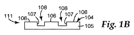
図1A〜1Gは、ポリマーフィルム基材105上で第1物質110をパターニングする例示的な方法の概略図である。ポリマー基材105は、機械的用具120で複製(100)されて、凹部領域108と、隣接する隆起領域106と、を含むレリーフパターンの付いた主要表面104を有する構造化ポリマー基材111を形成する。機械的用具120は、ポリマー基材105の主要表面104に(下向きの矢印で表されるようにして)適用することができる。機械的用具120は、ポリマー基材105の主要表面104の中に広がる凹部領域108を形成する。凹部領域108は、凹部表面107で画定される深さ及び幅を有する。いくつかの実施形態では、凹部領域108は、0.1〜10マイクロメートルの範囲の深さと、0.25〜50マイクロメートルの範囲の幅とを有する、概ね平行なチャネルであり、隣接する平行な凹部領域108間の距離は、100マイクロメートル〜1センチメートルの範囲である。
1A-1G are schematic views of an exemplary method for patterning a
ポリマーフィルム基材105は、上記のような、有用ないかなるポリマー材料からも形成することができる。多くの実施形態では、ポリマー基材105は、(図3に示す)ロールツーロール装置で利用可能な可撓性のポリマーフィルムである。いくつかの実施形態では、ポリマー基材105は、(図3に示す)ロールツーロール装置で利用可能な、可撓性で所望により透明なポリマーフィルムである。
The
第1物質110を、ポリマー基材105の隆起領域106と凹部領域108とを含む主要表面104に堆積することで、コーティングされたポリマー基材112が形成される。多くの実施形態では、第1物質110は、上記のような金属層である。
The
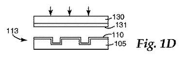
機能化材料の層131は、隆起領域106上に選択的に形成(113)されて、機能化された隆起領域106と機能化されていない凹部領域108とを形成する。機能化材料の層131は、エラストマーであり得る、形状のないプレート130を用いて、隆起領域106に適用することができる。形状のないプレート130は、機能化材料131を、形状のないプレート130が隆起領域106と接触しているその隆起領域106に転写する。形状のないプレート130は、機能化材料131を凹部領域108に転写しない。というのも、形状のないプレート130は凹部表面107と接触しないためである。このように、ポリマー基材105のレリーフパターンは、機能化材料131が選択的に転写される領域を決定する。多くの実施形態では、機能化材料は、上記のような自己組織化単層131である。
A
選択的に機能化されたポリマー基材114を、次に、物質110を機能化されていない凹部領域108から選択的にエッチングする液状エッチング溶液160に曝露(115)して、第1物質のパターニングされたポリマー基材116を形成する。一実施形態では、第1物質110は金を含む。多くの実施形態では、選択的なエッチング工程の後で機能化材料の層131のうち少なくとも一部を取り除くことができる。
The selectively functionalized
図2A〜2Fは、ポリマーフィルム基材200上で物質210をパターニングする別の例示的な方法の概略図である。例示的なポリマー基材200には2つ以上のポリマー層が含まれており、第1ポリマー層204はベース層であり、その第1層204の上には第2層205が配置されている。第1ポリマー層204及び第2ポリマー層205は、同じ又は異なるポリマー材料から形成することができる。いくつかの実施形態では、第1ポリマー層204は、ポリエチレンテレフタレート又はポリエチレンナフタレートなどのポリエステルから形成され、第2ポリマー層205は、ポリアクリレートから形成されている。多くの実施形態では、第1ポリマー層204及び第2ポリマー層205はフィルム又はウェブを形成している。多くの実施形態では、ポリマー基材200は、(図3に示す)ロールツーロール装置で利用可能な、可撓性で所望により透明なポリマーフィルムである。
2A-2F are schematic illustrations of another exemplary method for patterning
ポリマー基材200は、主要表面203から突出している1つ以上の隆起領域208を含むレリーフパターンの付いた主要表面203を有しており、1つ以上の凹部領域206は隆起領域208と隣接している。隆起領域208は、本明細書で説明する複製方法のうちいずれかで形成することができる。隆起領域208は、隆起領域表面207で画定されている。隆起領域208は、隆起領域表面207で画定される高さ及び幅を有する。いくつかの実施形態では、隆起領域208は、0.1〜10マイクロメートルの範囲の高さと、0.25マイクロメートル〜2ミリメートルの範囲の幅とを有する、概ね平行な隆起部であって、隣接する平行な隆起領域208間の距離は、0.25マイクロメートル〜1センチメートルの範囲である。
The
第1物質210を凹部領域206と隆起領域208とに堆積することで、コーティングされたポリマーフィルム基材211が形成される。多くの実施形態では、第1物質210は、上記のような金属層である。
Depositing the
機能化材料の層231は、隆起領域208上に選択的に形成(212)されて、機能化された隆起領域表面207と機能化されていない凹部領域206とを形成する。機能化材料の層231は、エラストマーであり得る、形状のないプレート230を用いて、隆起領域208に適用することができる。形状のないプレート230は、機能化材料231を、形状のないプレート230が隆起領域208と接触するその隆起領域208に転写する。形状のないプレート230は、機能化材料231を凹部領域206には転写しない。というのも、形状のないプレート230は凹部領域206と接触しないためである。このように、ポリマーフィルム基材のレリーフ構造は、機能化材料231が選択的に転写される領域を決定する。多くの実施形態では、機能化材料は、上記のような自己組織化単層231である。
A layer of
選択的に機能化されたポリマー基材213を次に、物質210を機能化されていない凹部領域106から選択的にエッチングする液状エッチング溶液260に曝露して、第1物質のパターニングされたポリマー基材215を形成する。一実施形態では、第1物質110は金を含む。多くの実施形態では、選択的なエッチング工程の後で、機能化材料の層231のうち少なくとも一部を取り除くことができる。
The selectively functionalized
図3は、例示的なロールツーロール装置300の概略図である。例示されるロールツーロール装置300には、投入ロール310と、巻取りロール320と、ポリマーフィルム311とが含まれている。図1及び図2で例示した方法は、ポリマーフィルム311上の箱330で実施することができる。パターニングされたポリマー基材又はフィルム312は、図示するように、巻取りロールに巻き取られて、要求に応じて更に加工することが可能である。
FIG. 3 is a schematic diagram of an exemplary roll-to-
ポリマー基材上でパターニングされた第1物質は、基材表面上で、ある領域の形及びある領域の大きさ、並びに厚さを有すると説明することができる。パターニングされた第1物質の領域の形状は、基材上で規則正しい又は反復する幾何学的配置、例えば、パターニングされた第1物質の多角形の配列、又は多角形の配列を含む不連続なエッチングされた領域の境界を画定する、パターニングされた第1物質のトレースのパターンを示すことができる。他の実施形態では、パターニングされた第1物質の形は、基材上で無作為な配置、例えば、エッチングされた領域のための不規則な形の境界を画定する、無作為な網目状のトレースを示してもよい。更に別の実施形態では、パターニングされた第1物質の形は、規則的でない、反復しない、又は無作為ではない配置であるが、対称的又は反復する幾何学的要素を含むか又はそれらを有さない特定のデザインである配置を示す場合もある。一実施形態では、光透過性のEMIシールド材料を作製するのに有用な、パターニングされた第1物質に関する形は、正方形グリッドであって、幅と厚さとピッチとで特徴付けられるパターニングされた第1物質のトレースを含むものである。光透過性のEMIシールド材料を作製するのに有用な他の形としては、正六角形の形状をもつ空き領域を画定し、かつぎっしり詰まった状態で配置された、連続的な金属トレースが挙げられる。正方形グリッド形状の連続的な金属トレースを作製するために、ポリマーフィルム基材に有用なレリーフパターンとしては、凹んだ正方形領域の正方形配列(グリッドと平行に配向したもの)が挙げられる。六角形の網目状の連続的な金属トレースを作製するために、ポリマーフィルム基材に有用なレリーフパターンとしては、凹んだ六角形領域の六角形配列(縁部は網目トレース方向と平行に配向されている)が挙げられる。まとめると、堆積した伝導体のEMIシールドパターンを作製する場合、幾つかの有用なレリーフパターンは、近接する隆起領域でそれぞれが囲まれた不連続な凹部領域の配列を含んでいる。 The first material patterned on the polymer substrate can be described as having a region shape and a region size and thickness on the substrate surface. The shape of the patterned first material region is a regular or repetitive geometric arrangement on the substrate, for example, a polygonal array of patterned first materials, or a discontinuous etch that includes a polygonal array. The pattern of the patterned first material trace defining the boundaries of the patterned region can be shown. In other embodiments, the patterned first material shape is a random mesh on the substrate, eg, defining a random shaped boundary for etched areas. A trace may be shown. In yet another embodiment, the patterned first material form is an irregular, non-repeating, or non-random arrangement, but includes or has symmetrical or repeating geometric elements. It may also indicate an arrangement that is not a specific design. In one embodiment, the shape for the first patterned material useful for making a light transmissive EMI shielding material is a square grid, characterized by a patterned first characterized by width, thickness and pitch. Includes one substance trace. Other shapes useful for making a light transmissive EMI shielding material include continuous metal traces that define a vacant area having a regular hexagonal shape and are arranged in a tightly packed manner. . Relief patterns useful for polymer film substrates to make square grid-shaped continuous metal traces include a square array of recessed square regions (oriented parallel to the grid). To create hexagonal mesh-like continuous metal traces, a useful relief pattern for polymer film substrates is a hexagonal array of recessed hexagonal regions (the edges are oriented parallel to the mesh trace direction. Are). In summary, when creating an EMI shield pattern of deposited conductors, some useful relief patterns include an array of discontinuous recessed areas, each surrounded by adjacent raised areas.
金属ワイヤグリッド偏光器構造物(例えば、可視光用)を作製するためには、その幅と間隔が、偏光が望まれる光の波長よりも小さいか、又は偏光が望まれる光の波長の三分の一未満であるか、又は偏光が望まれる光の波長の十分の一未満である、平行な隆起部の配列を含むレリーフパターンが有用である。多くの実施形態では、隆起部の高さは、幅の四分の一〜幅の10倍の範囲である。 To make a metal wire grid polarizer structure (eg, for visible light), the width and spacing are less than the wavelength of light that is desired to be polarized, or three times the wavelength of light that is desired to be polarized. Relief patterns comprising an array of parallel ridges that are less than one or less than one tenth of the wavelength of light for which polarization is desired are useful. In many embodiments, the height of the ridge ranges from a quarter of the width to 10 times the width.
幾つかの実施形態では、パターニングされた第1物質の形に関する最小領域寸法、例えば、パターニングされた第1物質の直線トレースの幅は、100ナノメートル〜1ミリメートル、又は500ナノメートル〜50マイクロメートル、又は1マイクロメートル〜25マイクロメートル、又は1マイクロメートル〜15マイクロメートル、又は0.5〜10マイクロメートルの範囲であることができる。光透過性EMIシールド材料を作製するための一つの例示的な実施形態では、パターニングされた第1物質の直線トレースの幅は、5マイクロメートル〜15マイクロメートル、又は0.5〜10マイクロメートルの範囲であり、厚さは、0.5〜10マイクロメートル、又は1マイクロメートル〜5マイクロメートルの範囲であり、ピッチは、25マイクロメートル〜1ミリメートル、又は100〜500マイクロメートルの範囲である。上記のパターニングされた第1物質の形に関する最大領域寸法、例えば、パターニングされた第1物質の直線トレースの長さは、1マイクロメートル〜5メートル、又は10マイクロメートル〜1メートルまでの範囲であることができる。光透過性EMIシールド材料である、EMIシールド材料のシートを作製する場合、パターニングされた第1物質の直線トレースの長さは、例えば、1センチメートル〜1メートルの範囲であることができる。 In some embodiments, the minimum area dimension for the shape of the patterned first material, for example, the width of the linear trace of the patterned first material is 100 nanometers to 1 millimeter, or 500 nanometers to 50 micrometers. Or from 1 micrometer to 25 micrometers, or from 1 micrometer to 15 micrometers, or from 0.5 to 10 micrometers. In one exemplary embodiment for making a light transmissive EMI shield material, the width of the patterned first material linear trace is between 5 micrometers and 15 micrometers, or between 0.5 and 10 micrometers. Range, thickness ranges from 0.5 to 10 micrometers, or from 1 micrometer to 5 micrometers, and pitch ranges from 25 micrometers to 1 millimeter, or from 100 to 500 micrometers. The maximum area dimension for the shape of the patterned first material, for example, the length of the linear trace of the patterned first material, ranges from 1 micrometer to 5 meters, or from 10 micrometers to 1 meter. be able to. When making a sheet of EMI shielding material, which is a light transmissive EMI shielding material, the length of the patterned linear trace of the first material can range, for example, from 1 centimeter to 1 meter.
本発明は、本明細書に記載した特定の実施例に限定されるとみなされるべきではなく、むしろ、特許請求の範囲に明記するような本発明の全ての態様を網羅するものと理解されるべきである。本明細書を検討すると、本発明が対象とする当業者には、様々な修正や等価の方法だけでなく、本発明を適用できる多数の構造も容易に明らかとなるであろう。 The present invention should not be considered limited to the particular embodiments described herein, but rather is understood to cover all aspects of the invention as set forth in the claims. Should. Upon review of this specification, it will be readily apparent to those skilled in the art to which the present invention is directed, not only the various modifications and equivalent methods, but also numerous structures to which the present invention can be applied.
別段の注記のない限り、化学試薬及び溶媒は、ウィスコンシン州ミルウォーキー(Milwaukee)のアルドリッチ・ケミカル社(Aldrich Chemical Co.)から入手したか又は入手可能なものである。 Unless otherwise noted, chemical reagents and solvents were obtained or available from Aldrich Chemical Co., Milwaukee, Wis.
実施例1
基材の調製
透明なポリカーボネートの250マイクロメートル厚のフィルム(コネチカット州フェアフィールド(Fairfield)のゼネラル・エレクトリック社(GE Plastics division)のGEプラスチックス事業部(General Electric Company)(マサチューセッツ州ピッツフィールド(Pittsfield))から商標名レキサン(Lexan)として入手可能)を、隆起した正方形で補完した凹部グリッドラインのレリーフパターンを用いて加熱エンボス加工に付した。エンボス加工用具は、直径10センチメートルの溶融石英の円形プレートから、光リソグラフィーと反応性イオンエッチング法とを用いて製造した。この用具は、幅が10マイクロメートル及び高さが約10マイクロメートルの隆起部であって、正方形グリッドのラインを200マイクロメートルピッチで画定する隆起部を含んでいた。エンボス加工は、モデル・オートM(Model AUTO M)積層プレス機(インディアナ州ウォバッシュ(Wabash)のカーバー社(Carver, Inc.)から入手可能)を用いて、エンボス加工用具をポリカーボネートフィルムに対して176℃で15分間10,000ニュートンの力で押圧することによって実施した。エンボス加工したフィルムには、幅が10マイクロメートル及び深さが約10マイクロメートルのチャネルであって、正方形グリッドのラインを200マイクロメートルピッチで画定するチャネルが含まれていた。エンボス加工した時点で、ポリカーボネートフィルムは、15オングストロームのチタン層を蒸着することによって先ず金属化して連結層を形成し、次いで加熱蒸発装置(ペンシルバニア州ピッバーグ(Pittsburgh)のカート・J・レスカー社(Kurt J. Lesker Co.)から入手可能)を用いて600オングストロームの金層を形成した。
Example 1
Substrate Preparation A 250 micrometer thick film of clear polycarbonate (GE Electrics division, General Electric Company, Fairfield, Connecticut, General Electric Company, Pittsfield, Mass.) )) Under the trade name Lexan) was subjected to hot embossing using a relief pattern of recessed grid lines complemented by raised squares. The embossing tool was manufactured from a fused quartz circular plate with a diameter of 10 centimeters using photolithography and reactive ion etching. The tool included a ridge that was 10 micrometers wide and about 10 micrometers high, defining a square grid of lines at a 200 micrometer pitch. The embossing is performed using a Model AUTO M laminating press (available from Carver, Inc., Wabash, Indiana) and the embossing tool is 176 against polycarbonate film. It was carried out by pressing with a force of 10,000 Newton at 15 ° C. for 15 minutes. The embossed film contained channels that were 10 micrometers wide and about 10 micrometers deep and defined a square grid of lines at a 200 micrometer pitch. When embossed, the polycarbonate film is first metallized by depositing a 15 Angstrom titanium layer to form a tie layer, and then a heating evaporator (Kurt J. Resker, Pittsburgh, PA). J. Lesker Co.) was used to form a 600 Å gold layer.
エラストマープレートの調製
ポリジメチルシロキサン(PDMS、ミシガン州ミッドランド(Midland)のダウ・コーニング社(Dow Corning Corporation)製のシルガード(Sylgard)(登録商標)184)の本質的に形状のないプレート2枚をシリコン単結晶に向けて投じた。プレートを飽和させるために、一方のプレートを、成型した平坦な面を大気に曝露しながら、5ミリモル濃度のオクタデカンチオールのエタノール溶液に2日間部分的に沈めた。続いて、二枚目のプレートを一枚目のプレートと手で接触させて、一枚目のプレートの上に30分間配置することで、二枚目のプレートのインク面を作製した。
Preparation of Elastomer Plates Silicone two essentially flat plates of polydimethylsiloxane (PDMS, Sylgard (R) 184 from Dow Corning Corporation, Midland, Mich.) Poured towards a single crystal. In order to saturate the plates, one plate was partially submerged in 5 mM octadecanethiol ethanol solution for 2 days with the molded flat surface exposed to the atmosphere. Subsequently, the second plate was brought into contact with the first plate by hand, and placed on the first plate for 30 minutes, thereby producing the ink surface of the second plate.
次にポリカーボネートフィルムの金属化されて構造化された表面を、二枚目のプレートのインク面と手で接触させて配置することで、オクタデカンチオールの自己組織化単層(SAM)をポリカーボネートフィルムの隆起領域に転写し、10マイクロメートル幅の溝(又はチャネル)は機能化されない(SAM無し)ままにした。 Next, the metallized and structured surface of the polycarbonate film is placed in manual contact with the ink surface of the second plate to form a self-assembled monolayer (SAM) of octadecanthiol on the polycarbonate film. Transfer to the raised area and leave the 10 micrometer wide groove (or channel) unfunctionalized (no SAM).
エッチング
SAM印刷された基材(機能化されていない10マイクロメートル幅の溝を有するもの)は、その後、液状エッチング液に15分間沈めることで、構造化された基材の凹部領域から金を取り除くことができる。金用の液状エッチング液は、例えば、0.02モル濃度の硝酸第二鉄と0.03モル濃度のチオ尿素との水溶液であり得る。
Etching SAM printed substrates (with non-functionalized 10 micrometer wide grooves) are then submerged in a liquid etchant for 15 minutes to remove gold from the recessed regions of the structured substrate. be able to. The liquid etchant for gold can be, for example, an aqueous solution of 0.02 molar ferric nitrate and 0.03 molar thiourea.
得られた基材は、その主要表面に金をパターン形態で有する可撓性の構造化された基材であり、そのパターンの形状は、構造化された基材の、金を有さない凹部領域で画定される。 The resulting substrate is a flexible structured substrate having gold in a pattern form on its main surface, and the pattern shape is a concave portion of the structured substrate that does not have gold Defined by regions.
Claims (20)
凹部領域と、隣接する隆起領域と、を含むレリーフパターンの付いた主要表面を有する、ポリマーフィルム基材を提供する工程と、
前記ポリマーフィルム基材の前記主要表面上に第1物質を堆積させて、コーティングされたポリマーフィルム基材を形成する工程と、
前記コーティングされたポリマーフィルム基材の前記隆起領域の上に機能化材料の層を選択的に形成して、機能化された隆起領域と機能化されていない凹部領域とを形成する工程と、
前記ポリマー基材の機能化されていない凹部領域から前記第1物質を選択的にエッチングして、第1物質のパターニングされたポリマー基材を形成する工程と、を含む、方法。 A method of patterning a first material on a polymer substrate, the method comprising:
Providing a polymer film substrate having a major surface with a relief pattern comprising a recessed region and an adjacent raised region;
Depositing a first material on the major surface of the polymer film substrate to form a coated polymer film substrate;
Selectively forming a layer of functionalized material on the raised areas of the coated polymer film substrate to form functionalized raised areas and non-functionalized recessed areas;
Selectively etching the first material from a non-functionalized recessed region of the polymer substrate to form a patterned polymer substrate of the first material.
前記ポリマーフィルムが、隆起領域と、隣接する凹部領域と、を含むレリーフ構造の付いた主要表面を有し、
前記隆起領域が第1物質で選択的にコーティングされており、前記第1物質が機能化分子を担持している、物品。 An article comprising a polymer film,
The polymer film has a major surface with a relief structure comprising a raised region and an adjacent recessed region;
An article wherein the raised areas are selectively coated with a first material, the first material carrying functionalized molecules.
Applications Claiming Priority (3)
| Application Number | Priority Date | Filing Date | Title |
|---|---|---|---|
| US11/550,542 US8764996B2 (en) | 2006-10-18 | 2006-10-18 | Methods of patterning a material on polymeric substrates |
| US11/550,542 | 2006-10-18 | ||
| PCT/US2007/081390 WO2008048928A2 (en) | 2006-10-18 | 2007-10-15 | Methods of patterning a material on polymeric substrates |
Publications (3)
| Publication Number | Publication Date |
|---|---|
| JP2010507261A true JP2010507261A (en) | 2010-03-04 |
| JP2010507261A5 JP2010507261A5 (en) | 2010-11-25 |
| JP5437808B2 JP5437808B2 (en) | 2014-03-12 |
Family
ID=39166986
Family Applications (1)
| Application Number | Title | Priority Date | Filing Date |
|---|---|---|---|
| JP2009533464A Expired - Fee Related JP5437808B2 (en) | 2006-10-18 | 2007-10-15 | Method for patterning a material on a polymer substrate |
Country Status (5)
| Country | Link |
|---|---|
| US (1) | US8764996B2 (en) |
| EP (1) | EP2082629A2 (en) |
| JP (1) | JP5437808B2 (en) |
| CN (1) | CN101530010A (en) |
| WO (1) | WO2008048928A2 (en) |
Cited By (3)
| Publication number | Priority date | Publication date | Assignee | Title |
|---|---|---|---|---|
| JP2011007875A (en) * | 2009-06-23 | 2011-01-13 | Asahi Kasei E-Materials Corp | Wire grid polarizing plate |
| JP2014094467A (en) * | 2012-11-08 | 2014-05-22 | Mitsubishi Plastics Inc | Polyester film for transparent conductive film substrate and transparent conductive film |
| KR20160063368A (en) * | 2013-09-30 | 2016-06-03 | 쓰리엠 이노베이티브 프로퍼티즈 캄파니 | Protective coating for printed conductive pattern on patterned nanowire transparent conductors |
Families Citing this family (36)
| Publication number | Priority date | Publication date | Assignee | Title |
|---|---|---|---|---|
| JP4109117B2 (en) * | 2001-03-01 | 2008-07-02 | シーメンス アクチエンゲゼルシヤフト | Solid comprising a surface layer and an adhesive film covered |
| US9164037B2 (en) * | 2007-01-26 | 2015-10-20 | Palo Alto Research Center Incorporated | Method and system for evaluation of signals received from spatially modulated excitation and emission to accurately determine particle positions and distances |
| US8821799B2 (en) | 2007-01-26 | 2014-09-02 | Palo Alto Research Center Incorporated | Method and system implementing spatially modulated excitation or emission for particle characterization with enhanced sensitivity |
| US8222518B2 (en) * | 2007-03-29 | 2012-07-17 | Kelly Thomas L | Photovoltaic roofing panel |
| US7879390B2 (en) * | 2007-05-30 | 2011-02-01 | Palo Alto Research Center Incorporated | Surface energy control methods for color filter printing |
| US8318552B2 (en) * | 2007-06-28 | 2012-11-27 | 3M Innovative Properties Company | Method for forming gate structures |
| US8373860B2 (en) | 2008-02-01 | 2013-02-12 | Palo Alto Research Center Incorporated | Transmitting/reflecting emanating light with time variation |
| US8629981B2 (en) | 2008-02-01 | 2014-01-14 | Palo Alto Research Center Incorporated | Analyzers with time variation based on color-coded spatial modulation |
| EP2257969B1 (en) | 2008-02-28 | 2017-12-20 | 3M Innovative Properties Company | Methods of patterning a conductor on a substrate |
| EP2260367A4 (en) | 2008-02-28 | 2014-05-14 | 3M Innovative Properties Co | Touch screen sensor with low visibility conductors |
| JP2011514597A (en) | 2008-02-28 | 2011-05-06 | スリーエム イノベイティブ プロパティズ カンパニー | Touch screen sensor with varying sheet resistance |
| KR20100137483A (en) * | 2008-02-28 | 2010-12-30 | 쓰리엠 이노베이티브 프로퍼티즈 컴파니 | Touch screen sensor |
| US8284332B2 (en) * | 2008-08-01 | 2012-10-09 | 3M Innovative Properties Company | Touch screen sensor with low visibility conductors |
| US8580344B2 (en) * | 2008-03-17 | 2013-11-12 | Intermolecular, Inc. | Stamp usage to enhance surface layer functionalization and selectivity |
| US8858813B2 (en) * | 2008-12-11 | 2014-10-14 | 3M Innovative Properties Company | Patterning process |
| JP5464574B2 (en) * | 2009-03-31 | 2014-04-09 | 日本写真印刷株式会社 | Transparent conductive sheet and manufacturing method thereof, decorative molded product |
| WO2010144762A1 (en) * | 2009-06-12 | 2010-12-16 | Lord Corporation | Method for protecting a substrate from lightning strikes |
| JP6128847B2 (en) | 2009-06-25 | 2017-05-17 | スリーエム イノベイティブ プロパティズ カンパニー | Wet etching method for self-assembled monolayer patterned substrate and metal patterned article |
| US8553400B2 (en) | 2009-06-30 | 2013-10-08 | 3M Innovative Properties Company | Electronic displays and metal micropatterned substrates having a graphic |
| EP2273324A1 (en) * | 2009-07-06 | 2011-01-12 | ETA SA Manufacture Horlogère Suisse | Method for manufacturing a decorated part with raised pattern |
| KR101197776B1 (en) * | 2010-12-27 | 2012-11-06 | 엘지이노텍 주식회사 | method for manufacturing wire grid polarizer |
| KR101757241B1 (en) | 2010-12-29 | 2017-07-26 | 엘지디스플레이 주식회사 | Nano-wire grid polarizing plate, method of fabricating the same, and liquid crystal display device including the same |
| KR101771138B1 (en) * | 2011-05-13 | 2017-08-25 | 삼성전자주식회사 | Wire grid polarizer, method of fabricating the wire grid polarizer and display panel including the wire grid polarizer |
| US9029800B2 (en) | 2011-08-09 | 2015-05-12 | Palo Alto Research Center Incorporated | Compact analyzer with spatial modulation and multiple intensity modulated excitation sources |
| US8723140B2 (en) | 2011-08-09 | 2014-05-13 | Palo Alto Research Center Incorporated | Particle analyzer with spatial modulation and long lifetime bioprobes |
| CN102627856B (en) * | 2012-04-01 | 2015-01-07 | 云南云天化股份有限公司 | Polyimide film of high-peel-strength flexible printed circuit board, preparation method thereof and printed circuit board made of polyimide film |
| JP5224203B1 (en) | 2012-07-11 | 2013-07-03 | 大日本印刷株式会社 | Touch panel sensor, touch panel device, and display device |
| KR102042822B1 (en) * | 2012-09-24 | 2019-11-08 | 한국전자통신연구원 | An electronic circuit and method for fabricating the same |
| US9167700B2 (en) * | 2013-03-05 | 2015-10-20 | Eastman Kodak Company | Micro-channel connection method |
| US20140338191A1 (en) * | 2013-05-15 | 2014-11-20 | Uni-Pixel Displays, Inc. | Method of manufacturing an integrated touch sensor with decorative color graphics |
| KR20150009846A (en) * | 2013-07-17 | 2015-01-27 | 삼성디스플레이 주식회사 | Touch Screen Panel and Fabricating Method Thereof |
| EP3084523B1 (en) | 2013-12-19 | 2019-07-03 | Illumina, Inc. | Substrates comprising nano-patterning surfaces and methods of preparing thereof |
| JP2019197423A (en) * | 2018-05-10 | 2019-11-14 | シャープ株式会社 | Substrate manufacturing method and display device manufacturing method |
| CN112300627B (en) * | 2019-07-26 | 2022-05-31 | 北京梦之墨科技有限公司 | Application of metal-phobic material |
| KR20210030145A (en) * | 2019-09-09 | 2021-03-17 | 엘지디스플레이 주식회사 | Display Device with Touch Screen |
| CN114515516B (en) * | 2022-01-27 | 2023-07-07 | 南京工业大学 | High-flux corrugated PDMS nanofiber composite membrane and preparation method thereof |
Citations (9)
| Publication number | Priority date | Publication date | Assignee | Title |
|---|---|---|---|---|
| JPS63285995A (en) * | 1987-05-19 | 1988-11-22 | Sankyo Kasei Kk | Circuit substrate |
| JPH0476985A (en) * | 1990-07-18 | 1992-03-11 | Cmk Corp | Manufacture of printed circuit board |
| JP2000174486A (en) * | 1998-12-04 | 2000-06-23 | Sumitomo Rubber Ind Ltd | Light-transmission electromagnetic wave shield film and manufacturing method of light-transmission electromagnetic shield panel |
| JP2002294469A (en) * | 2001-03-26 | 2002-10-09 | Internatl Business Mach Corp <Ibm> | Method for selectively etching sam substrate |
| JP2004146536A (en) * | 2002-10-23 | 2004-05-20 | Mitsui Chemicals Inc | Filter for display |
| JP2004241761A (en) * | 2003-01-16 | 2004-08-26 | Dainippon Printing Co Ltd | Sheet for electromagnetic wave shielding and manufacturing method therefor |
| JP2006060171A (en) * | 2004-08-24 | 2006-03-02 | Toppan Printing Co Ltd | Blackening treatment apparatus |
| WO2006061741A2 (en) * | 2004-12-06 | 2006-06-15 | Koninklijke Philips Electronics N.V. | Etchant solutions and additives therefor |
| JP2006261322A (en) * | 2005-03-16 | 2006-09-28 | Jsr Corp | Electromagnetic wave shield film and its manufacturing method |
Family Cites Families (67)
| Publication number | Priority date | Publication date | Assignee | Title |
|---|---|---|---|---|
| US2963748A (en) | 1957-05-27 | 1960-12-13 | Young Lawrence John | Printed circuits |
| US3075280A (en) | 1959-10-19 | 1963-01-29 | Bell Telephone Labor Inc | Method of making printed wiring assemblies |
| US3620933A (en) | 1969-12-31 | 1971-11-16 | Macdermid Inc | Forming plastic parts having surfaces receptive to adherent coatings |
| US3800020A (en) | 1972-03-23 | 1974-03-26 | Cramer P Co | Method of making a circuit board |
| CH591570A5 (en) | 1972-11-28 | 1977-09-30 | Buser Ag Maschf Fritz | |
| US3952152A (en) | 1974-10-29 | 1976-04-20 | Teletype Corporation | CRT shield |
| US4179797A (en) | 1978-03-23 | 1979-12-25 | Xerox Corporation | Method of making a resistor array |
| FR2430847A1 (en) | 1978-07-13 | 1980-02-08 | Saint Gobain | HEATING AND / OR ALARM GLASS |
| US4576850A (en) | 1978-07-20 | 1986-03-18 | Minnesota Mining And Manufacturing Company | Shaped plastic articles having replicated microstructure surfaces |
| US4381421A (en) | 1980-07-01 | 1983-04-26 | Tektronix, Inc. | Electromagnetic shield for electronic equipment |
| US4412255A (en) | 1981-02-23 | 1983-10-25 | Optical Coating Laboratory, Inc. | Transparent electromagnetic shield and method of manufacturing |
| US4510347A (en) | 1982-12-06 | 1985-04-09 | Fine Particles Technology Corporation | Formation of narrow conductive paths on a substrate |
| US5094811A (en) | 1983-09-21 | 1992-03-10 | Allied-Signal | Method of making a printed circuit board |
| US5061438A (en) | 1983-09-21 | 1991-10-29 | Allied-Signal Inc. | Method of making a printed circuit board |
| US4775611A (en) | 1983-11-10 | 1988-10-04 | Sullivan Donald F | Additive printed circuit boards with flat surface and indented primary wiring conductors |
| AU570309B2 (en) | 1984-03-26 | 1988-03-10 | Unisearch Limited | Buried contact solar cell |
| US4552615A (en) | 1984-05-21 | 1985-11-12 | International Business Machines Corporation | Process for forming a high density metallurgy system on a substrate and structure thereof |
| US4614837A (en) | 1985-04-03 | 1986-09-30 | Allied Corporation | Method for placing electrically conductive paths on a substrate |
| CA1293918C (en) * | 1987-01-26 | 1992-01-07 | Donald E. Beckett | Element for microwave heating |
| US4869930A (en) | 1987-07-10 | 1989-09-26 | International Business Machines Corporation | Method for preparing substrates for deposition of metal seed from an organometallic vapor for subsequent electroless metallization |
| DE3832299A1 (en) | 1988-09-20 | 1990-03-22 | Schering Ag | Method for producing a three-dimensional conductor moulding having a recessed conductor-track layout |
| US5462624A (en) | 1992-12-22 | 1995-10-31 | Vlsi Technology, Inc. | Embedded inter-connect frame |
| US5399879A (en) | 1993-02-05 | 1995-03-21 | National Research Council Of Canada | Long wavelength IR photo-induced switching of a resonant tunnelling diode using the intersubband transition |
| US5900160A (en) | 1993-10-04 | 1999-05-04 | President And Fellows Of Harvard College | Methods of etching articles via microcontact printing |
| US6180239B1 (en) | 1993-10-04 | 2001-01-30 | President And Fellows Of Harvard College | Microcontact printing on surfaces and derivative articles |
| US5512131A (en) | 1993-10-04 | 1996-04-30 | President And Fellows Of Harvard College | Formation of microstamped patterns on surfaces and derivative articles |
| US6776094B1 (en) | 1993-10-04 | 2004-08-17 | President & Fellows Of Harvard College | Kit For Microcontact Printing |
| US5595943A (en) | 1994-06-30 | 1997-01-21 | Hitachi, Ltd. | Method for formation of conductor using electroless plating |
| US6518168B1 (en) * | 1995-08-18 | 2003-02-11 | President And Fellows Of Harvard College | Self-assembled monolayer directed patterning of surfaces |
| US6060121A (en) | 1996-03-15 | 2000-05-09 | President And Fellows Of Harvard College | Microcontact printing of catalytic colloids |
| JPH1075038A (en) | 1996-06-28 | 1998-03-17 | Ngk Spark Plug Co Ltd | Wiring board and its manufacture method |
| US6048623A (en) * | 1996-12-18 | 2000-04-11 | Kimberly-Clark Worldwide, Inc. | Method of contact printing on gold coated films |
| US5932150A (en) | 1997-08-25 | 1999-08-03 | Holo-Source Corporation | Replication of diffraction images in oriented films |
| US6788463B2 (en) | 1998-01-13 | 2004-09-07 | 3M Innovative Properties Company | Post-formable multilayer optical films and methods of forming |
| JP2000223886A (en) | 1999-01-28 | 2000-08-11 | Nisshinbo Ind Inc | Perspective electromagnetic wave shield material and its manufacture |
| US6121150A (en) | 1999-04-22 | 2000-09-19 | Advanced Micro Devices, Inc. | Sputter-resistant hardmask for damascene trench/via formation |
| TW539763B (en) | 1999-06-18 | 2003-07-01 | Ibm | Method for printing a catalyst on substrates for electroless deposition |
| JP3503546B2 (en) | 1999-11-01 | 2004-03-08 | 信越化学工業株式会社 | Method of forming metal pattern |
| JP4013021B2 (en) | 1999-12-17 | 2007-11-28 | 松下電工株式会社 | Transparent electromagnetic shielding material and manufacturing method thereof |
| JP2001335952A (en) | 2000-05-31 | 2001-12-07 | Rikogaku Shinkokai | Electroless plating method, wiring device and its production method |
| US6442316B1 (en) * | 2000-12-21 | 2002-08-27 | Alcatel | Stress sensor based on periodically inserted color-changing tactile films to detect mishandling of fiber optic cables |
| US6599824B1 (en) | 2001-02-26 | 2003-07-29 | Advanced Micro Devices, Inc. | System for and method of forming local interconnect using microcontact printing |
| EP1393389B1 (en) | 2001-05-23 | 2018-12-05 | Flexenable Limited | Laser patterning of devices |
| US6737170B2 (en) | 2001-09-06 | 2004-05-18 | Toray Plastics (America), Inc. | Coated film with exceptional embossing characteristics and method for producing it |
| GB2381274A (en) | 2001-10-29 | 2003-04-30 | Qinetiq Ltd | High resolution patterning method |
| KR20040068572A (en) | 2001-12-06 | 2004-07-31 | 코닌클리즈케 필립스 일렉트로닉스 엔.브이. | Method for defining a source and a drain and a gap inbetween |
| US6828581B2 (en) | 2002-02-26 | 2004-12-07 | The United States Of America As Represented By The Secretary Of Commerce | Selective electroless attachment of contacts to electrochemically-active molecules |
| US6875475B2 (en) | 2002-04-01 | 2005-04-05 | William Marsh Rice University | Methods for producing submicron metal line and island arrays |
| US6911385B1 (en) | 2002-08-22 | 2005-06-28 | Kovio, Inc. | Interface layer for the fabrication of electronic devices |
| US6764885B2 (en) | 2002-10-17 | 2004-07-20 | Avery Dennison Corporation | Method of fabricating transistor device |
| GB0229191D0 (en) | 2002-12-14 | 2003-01-22 | Plastic Logic Ltd | Embossing of polymer devices |
| US7144608B2 (en) | 2003-01-24 | 2006-12-05 | Nitto Denko Corporation | Color correcting polarizer |
| US7001658B2 (en) | 2003-04-28 | 2006-02-21 | Eastman Kodak Company | Heat selective electrically conductive polymer sheet |
| JP2005032894A (en) | 2003-07-10 | 2005-02-03 | Hitachi Cable Ltd | Tape carrier for semiconductor device |
| GB0326904D0 (en) * | 2003-11-19 | 2003-12-24 | Koninkl Philips Electronics Nv | Formation of self-assembled monolayers |
| KR100590727B1 (en) * | 2004-02-24 | 2006-06-19 | 한국기계연구원 | Microcontact printing methods using imprinted nanostructure and Nanostructure thereof |
| KR100581221B1 (en) | 2004-06-30 | 2006-05-22 | 삼성전자주식회사 | Method of manufacturing tape substarte |
| US6932150B1 (en) * | 2004-09-10 | 2005-08-23 | Industrial Technology Research Institute | Heat-dissipation device |
| US7160583B2 (en) * | 2004-12-03 | 2007-01-09 | 3M Innovative Properties Company | Microfabrication using patterned topography and self-assembled monolayers |
| US7585424B2 (en) * | 2005-01-18 | 2009-09-08 | Hewlett-Packard Development Company, L.P. | Pattern reversal process for self aligned imprint lithography and device |
| GB2427509A (en) * | 2005-06-21 | 2006-12-27 | Seiko Epson Corp | Organic electronic device fabrication by micro-embossing |
| US7871670B2 (en) * | 2005-08-10 | 2011-01-18 | 3M Innovative Properties Company | Microfabrication using replicated patterned topography and self-assembled monolayers |
| US8109612B2 (en) | 2005-08-29 | 2012-02-07 | Fujifilm Corporation | Wiring substrate, method of manufacturing wiring substrate, and liquid droplet ejection head |
| CA2654973A1 (en) * | 2006-06-28 | 2008-07-31 | Northwestern University | Etching and hole arrays |
| US20080095988A1 (en) * | 2006-10-18 | 2008-04-24 | 3M Innovative Properties Company | Methods of patterning a deposit metal on a polymeric substrate |
| US7968804B2 (en) * | 2006-12-20 | 2011-06-28 | 3M Innovative Properties Company | Methods of patterning a deposit metal on a substrate |
| KR101468960B1 (en) * | 2008-07-16 | 2014-12-04 | 삼성전자주식회사 | Fabrication mehtod of lithography mask and formation method of fine pattern using the same |
-
2006
- 2006-10-18 US US11/550,542 patent/US8764996B2/en not_active Expired - Fee Related
-
2007
- 2007-10-15 JP JP2009533464A patent/JP5437808B2/en not_active Expired - Fee Related
- 2007-10-15 WO PCT/US2007/081390 patent/WO2008048928A2/en active Application Filing
- 2007-10-15 CN CNA2007800391003A patent/CN101530010A/en active Pending
- 2007-10-15 EP EP07854045A patent/EP2082629A2/en not_active Withdrawn
Patent Citations (9)
| Publication number | Priority date | Publication date | Assignee | Title |
|---|---|---|---|---|
| JPS63285995A (en) * | 1987-05-19 | 1988-11-22 | Sankyo Kasei Kk | Circuit substrate |
| JPH0476985A (en) * | 1990-07-18 | 1992-03-11 | Cmk Corp | Manufacture of printed circuit board |
| JP2000174486A (en) * | 1998-12-04 | 2000-06-23 | Sumitomo Rubber Ind Ltd | Light-transmission electromagnetic wave shield film and manufacturing method of light-transmission electromagnetic shield panel |
| JP2002294469A (en) * | 2001-03-26 | 2002-10-09 | Internatl Business Mach Corp <Ibm> | Method for selectively etching sam substrate |
| JP2004146536A (en) * | 2002-10-23 | 2004-05-20 | Mitsui Chemicals Inc | Filter for display |
| JP2004241761A (en) * | 2003-01-16 | 2004-08-26 | Dainippon Printing Co Ltd | Sheet for electromagnetic wave shielding and manufacturing method therefor |
| JP2006060171A (en) * | 2004-08-24 | 2006-03-02 | Toppan Printing Co Ltd | Blackening treatment apparatus |
| WO2006061741A2 (en) * | 2004-12-06 | 2006-06-15 | Koninklijke Philips Electronics N.V. | Etchant solutions and additives therefor |
| JP2006261322A (en) * | 2005-03-16 | 2006-09-28 | Jsr Corp | Electromagnetic wave shield film and its manufacturing method |
Cited By (5)
| Publication number | Priority date | Publication date | Assignee | Title |
|---|---|---|---|---|
| JP2011007875A (en) * | 2009-06-23 | 2011-01-13 | Asahi Kasei E-Materials Corp | Wire grid polarizing plate |
| JP2014094467A (en) * | 2012-11-08 | 2014-05-22 | Mitsubishi Plastics Inc | Polyester film for transparent conductive film substrate and transparent conductive film |
| KR20160063368A (en) * | 2013-09-30 | 2016-06-03 | 쓰리엠 이노베이티브 프로퍼티즈 캄파니 | Protective coating for printed conductive pattern on patterned nanowire transparent conductors |
| JP2016535433A (en) * | 2013-09-30 | 2016-11-10 | スリーエム イノベイティブ プロパティズ カンパニー | Protective coating for printed conductive patterns on patterned nanowire transparent conductors |
| KR102264357B1 (en) * | 2013-09-30 | 2021-06-15 | 쓰리엠 이노베이티브 프로퍼티즈 캄파니 | Protective coating for printed conductive pattern on patterned nanowire transparent conductors |
Also Published As
| Publication number | Publication date |
|---|---|
| WO2008048928A3 (en) | 2008-07-24 |
| CN101530010A (en) | 2009-09-09 |
| US8764996B2 (en) | 2014-07-01 |
| WO2008048928A2 (en) | 2008-04-24 |
| EP2082629A2 (en) | 2009-07-29 |
| US20080095985A1 (en) | 2008-04-24 |
| JP5437808B2 (en) | 2014-03-12 |
Similar Documents
| Publication | Publication Date | Title |
|---|---|---|
| JP5437808B2 (en) | Method for patterning a material on a polymer substrate | |
| US20100203248A1 (en) | Methods of patterning a deposit metal on a polymeric substrate | |
| JP5932872B2 (en) | Method for patterning deposited metal on a substrate | |
| JP6321716B2 (en) | Method for patterning a conductor on a substrate | |
| US7682703B2 (en) | Microfabrication using patterned topography and self-assembled monolayers | |
| EP2298046B1 (en) | Providing a plastic substrate with a metallic pattern | |
| EP2620523B1 (en) | Method of forming a microstructure | |
| TWI660858B (en) | Functional features, and microcontact printing stamps and articles with the same, and methods to produce them | |
| US9058084B2 (en) | Hybrid single-side touch screen | |
| KR20130122776A (en) | Patterned flexible transparent conductive sheet and manufacturing method thereof | |
| TW201132256A (en) | Formation of electrically conductive pattern by surface energy modification | |
| KR20060135310A (en) | Method for fabricating detail pattern by using soft mold | |
| KR100957487B1 (en) | Method for fabricating plastic electrode film | |
| Sneck et al. | Reverse-offset printing of polymer resist ink for micrometer-level patterning of metal and metal-oxide layers | |
| Cai et al. | Highly-facile template-based selective electroless metallization of micro-and nanopatterns for plastic electronics and plasmonics | |
| KR101856231B1 (en) | Transparent substrate with nano-pattern and method of manufacturing thereof | |
| CN107835974B (en) | Electronic device including through-hole and method of forming such electronic device |
Legal Events
| Date | Code | Title | Description |
|---|---|---|---|
| A521 | Request for written amendment filed |
Free format text: JAPANESE INTERMEDIATE CODE: A523 Effective date: 20101004 |
|
| A621 | Written request for application examination |
Free format text: JAPANESE INTERMEDIATE CODE: A621 Effective date: 20101004 |
|
| A977 | Report on retrieval |
Free format text: JAPANESE INTERMEDIATE CODE: A971007 Effective date: 20120426 |
|
| A131 | Notification of reasons for refusal |
Free format text: JAPANESE INTERMEDIATE CODE: A131 Effective date: 20120508 |
|
| A601 | Written request for extension of time |
Free format text: JAPANESE INTERMEDIATE CODE: A601 Effective date: 20120807 |
|
| A602 | Written permission of extension of time |
Free format text: JAPANESE INTERMEDIATE CODE: A602 Effective date: 20120814 |
|
| A521 | Request for written amendment filed |
Free format text: JAPANESE INTERMEDIATE CODE: A523 Effective date: 20121108 |
|
| A131 | Notification of reasons for refusal |
Free format text: JAPANESE INTERMEDIATE CODE: A131 Effective date: 20130326 |
|
| A521 | Request for written amendment filed |
Free format text: JAPANESE INTERMEDIATE CODE: A523 Effective date: 20130625 |
|
| TRDD | Decision of grant or rejection written | ||
| A01 | Written decision to grant a patent or to grant a registration (utility model) |
Free format text: JAPANESE INTERMEDIATE CODE: A01 Effective date: 20131112 |
|
| A61 | First payment of annual fees (during grant procedure) |
Free format text: JAPANESE INTERMEDIATE CODE: A61 Effective date: 20131212 |
|
| R150 | Certificate of patent or registration of utility model |
Ref document number: 5437808 Country of ref document: JP Free format text: JAPANESE INTERMEDIATE CODE: R150 Free format text: JAPANESE INTERMEDIATE CODE: R150 |
|
| R250 | Receipt of annual fees |
Free format text: JAPANESE INTERMEDIATE CODE: R250 |
|
| R250 | Receipt of annual fees |
Free format text: JAPANESE INTERMEDIATE CODE: R250 |
|
| R250 | Receipt of annual fees |
Free format text: JAPANESE INTERMEDIATE CODE: R250 |
|
| R250 | Receipt of annual fees |
Free format text: JAPANESE INTERMEDIATE CODE: R250 |
|
| LAPS | Cancellation because of no payment of annual fees |