JP2010251802A - Semiconductor manufacturing apparatus - Google Patents
Semiconductor manufacturing apparatus Download PDFInfo
- Publication number
- JP2010251802A JP2010251802A JP2010169180A JP2010169180A JP2010251802A JP 2010251802 A JP2010251802 A JP 2010251802A JP 2010169180 A JP2010169180 A JP 2010169180A JP 2010169180 A JP2010169180 A JP 2010169180A JP 2010251802 A JP2010251802 A JP 2010251802A
- Authority
- JP
- Japan
- Prior art keywords
- liquid
- temperature
- exposure
- resist film
- unit
- Prior art date
- Legal status (The legal status is an assumption and is not a legal conclusion. Google has not performed a legal analysis and makes no representation as to the accuracy of the status listed.)
- Granted
Links
Images


Abstract
Description
本発明は、半導体装置の製造プロセス等において用いられる半導体製造装置に関する。 The present invention relates to a semiconductor manufacturing apparatus used in a semiconductor device manufacturing process or the like.
半導体集積回路の大集積化及び半導体素子のダウンサイジングに伴って、リソグラフィ技術の開発の加速が望まれている。現在のところ、露光光としては、水銀ランプ、KrFエキシマレーザ又はArFエキシマレーザ等を用いる光リソグラフィによりパターン形成が行なわれていると共に、より短波長であるF2レーザの使用も検討されているが、露光装置及びレジスト材料における課題が未だ多く残されているため、より短波長の露光光を用いる光リソグラフィの実用化の時期は未だ先になっている。 Along with the large integration of semiconductor integrated circuits and the downsizing of semiconductor elements, it is desired to accelerate the development of lithography technology. At present, as exposure light, pattern formation is performed by optical lithography using a mercury lamp, a KrF excimer laser, an ArF excimer laser, or the like, and the use of an F 2 laser having a shorter wavelength is also being studied. However, since many problems still remain in the exposure apparatus and the resist material, the time for practical application of photolithography using exposure light having a shorter wavelength is still ahead.
このような状況から、最近従来の露光光を用いてパターンの一層の微細化を進めるべく、液浸リソグラフィ(immersion lithography)法(非特許文献1を参照。)が提案されている。 Under such circumstances, recently, an immersion lithography method (see Non-Patent Document 1) has been proposed in order to further refine a pattern using conventional exposure light.
この液浸リソグラフィ法によれば、露光装置内における投影レンズとウエハ上のレジスト膜との間の領域が屈折率がn(但し、n>1)である液体で満たされるため、露光装置のNA(開口数)の値がn・NAとなるので、レジスト膜の解像性が向上する。 According to this immersion lithography method, the area between the projection lens and the resist film on the wafer in the exposure apparatus is filled with a liquid having a refractive index of n (where n> 1), and therefore the NA of the exposure apparatus. Since the value of (numerical aperture) is n · NA, the resolution of the resist film is improved.
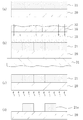
以下、従来の液浸リソグラフィを用いるパターン形成方法について図6(a)〜図6(d)を参照しながら説明する。 Hereinafter, a pattern forming method using conventional immersion lithography will be described with reference to FIGS. 6 (a) to 6 (d).
まず、以下の組成を有するポジ型の化学増幅型レジスト材料を準備する。 First, a positive chemically amplified resist material having the following composition is prepared.
ポリ((ターシャリーブチル=ノルボルネン−5−メチレンカルボキシレート)(50mol%)−(無水マレイン酸)(50mol%))(ベースポリマー)…………………………………………………2g
トリフェニルスルフォニウムノナフレート(酸発生剤)………………………0.06g
トリエタノールアミン(クエンチャー)………………………………………0.002g
プロピレングリコールモノメチルエーテルアセテート(溶媒)……………………20g
次に、図6(a)に示すように、基板1の上に前記の化学増幅型レジスト材料を塗布して、0.35μmの厚さを持つレジスト膜2を形成する。
Poly ((tertiary butyl = norbornene-5-methylenecarboxylate) (50mol%)-(maleic anhydride) (50mol%)) (base polymer) ………………………………………… ……… 2g
Triphenylsulfonium nonaflate (acid generator) …………………… 0.06g
Triethanolamine (quencher) ………………………………… 0.002g
Propylene glycol monomethyl ether acetate (solvent) ……………… 20g
Next, as shown in FIG. 6A, the chemically amplified resist material is applied onto the
次に、図6(b)に示すように、レジスト膜2と投影レンズ5との間に温度が室温の、例えば23℃程度の液体(水)3を配して、NAが0.68であるArFエキシマレーザよりなる露光光4をマスクを介してレジスト膜2に照射してパターン露光を行なう。
Next, as shown in FIG. 6B, a liquid (water) 3 having a temperature of room temperature, for example, about 23 ° C. is disposed between the
次に、図6(c)に示すように、パターン露光が行なわれたレジスト膜2に対して、ホットプレートにより105℃の温度下で60秒間加熱した後、濃度が0.26Nのテトラメチルアンモニウムハイドロキサイド現像液により現像を行なうと、図6(d)に示すように、レジスト膜2の未露光部よりなり0.09μmのライン幅を有するレジストパターン2aを得られる。
Next, as shown in FIG. 6C, the
ところが、図6(d)に示すように、従来の液浸リソグラフィを用いたパターン形成方法により得られるレジストパターン2aのパターン形状は不良であった。
However, as shown in FIG. 6 (d), the pattern shape of the
本願発明者らは、液浸リソグラフィにより得られるレジストパターンの形状が不良となる原因について種々の検討を重ねた結果、液浸用の液体3が露光中に蒸発することにより液体3と投影レンズ5との間に空隙ができ、この空隙により液体3の屈折率が変動してしまい、所定の解像度を得られなくなることから、パターン形状の不良をもたらすということを突き止めた。
The inventors of the present application have conducted various studies on the cause of the defective shape of the resist pattern obtained by immersion lithography, and as a result, the
従って、液体の一部が蒸発した液浸用の液体を介して行なった露光によってレジストパターンの形状が不良となり、不良な形状のレジストパターンを用いてエッチングを行なうと、被エッチング膜に得られるパターンの形状も不良となってしまうため、半導体装置の製造プロセスにおける生産性及び歩留まりが低下してしまうという問題を生じる。 Therefore, the resist pattern shape becomes defective due to the exposure performed through the immersion liquid in which a part of the liquid is evaporated, and when etching is performed using the resist pattern having a defective shape, the pattern obtained in the film to be etched This also causes a problem that the productivity and yield in the manufacturing process of the semiconductor device are reduced.
前記従来の問題に鑑み、本発明は、液浸リソグラフィにより得られるレジストパターンの形状を良好にできるようにすることを目的とする。 In view of the above-described conventional problems, an object of the present invention is to improve the shape of a resist pattern obtained by immersion lithography.
前記の目的を達成するため、本発明は、液浸リソグラフィを用いたパターン形成方法を、液浸用の液体に蒸発しにくい組成の液体を用いるか、または液浸用の液体を露光中に蒸発しにくい環境下で配する構成とする。また、半導体製造装置として、液浸用の液体を露光中に蒸発しにくい環境下においてパターン露光を行なう構成とする。 In order to achieve the above object, according to the present invention, a pattern forming method using immersion lithography uses a liquid having a composition that does not easily evaporate into an immersion liquid, or evaporates the immersion liquid during exposure. The configuration is arranged in an environment that is difficult to perform. In addition, the semiconductor manufacturing apparatus is configured to perform pattern exposure in an environment in which liquid for immersion is difficult to evaporate during exposure.
具体的に、本発明に係る第1のパターン形成方法は、基板の上にレジスト膜を形成する工程と、レジスト膜の上に不飽和脂肪酸を含む液体を配した状態で、レジスト膜に対して露光光を選択的に照射することによりパターン露光を行なう工程と、パターン露光が行なわれたレジスト膜に対して現像を行なってレジストパターンを形成する工程とを備えていることを特徴とする。 Specifically, the first pattern forming method according to the present invention includes a step of forming a resist film on a substrate, and a liquid containing an unsaturated fatty acid on the resist film. The method includes a step of performing pattern exposure by selectively irradiating exposure light and a step of developing the resist film on which pattern exposure has been performed to form a resist pattern.
第1のパターン形成方法によると、液浸用の液体に不飽和脂肪酸を含む液体を用いるため、添加された不飽和脂肪酸によって液浸用の液体が蒸発しにくくなる。これにより、液浸用の液体は露光中の蒸発で生じる空隙による屈折率の異常等が防止されるので、露光中の液体に所定の屈折率(露光特性)が維持される結果、液浸リソグラフィによるレジストパターンの形状を良好にすることができる。 According to the first pattern forming method, since the liquid containing the unsaturated fatty acid is used as the liquid for immersion, the liquid for immersion becomes difficult to evaporate due to the added unsaturated fatty acid. As a result, the liquid for immersion is prevented from anomalies in refractive index due to the voids generated by evaporation during exposure, so that a predetermined refractive index (exposure characteristics) is maintained in the liquid during exposure. The shape of the resist pattern can be improved.
本願発明者らは、不飽和脂肪酸は脂質が高いことにより、高い保湿作用を有するという知見を得ている。この保湿作用は、不飽和脂肪酸の炭素同士の2重結合又は3重結合による機能及びカルボン酸基に由来する機能による。炭素同士の2重結合又は3重結合は、単結合でつながる分子内において、特に炭素原子間に電子が集まり偏った状態になっている。また、カルボン酸基が有する炭素と酸素との2重結合は、電気陰性度が炭素よりも高い酸素との間での2重結合であるため、炭素同士の2重結合の場合よりも電子を多く引き付けるので、イオン性が高い状態となっている。その結果、イオン性が低い分子又は置換基との間であっても相互作用が生じやすく、特に液浸用の液体に含まれる水酸基とは相互作用を容易に起こす。その結果、不飽和脂肪酸は高い保湿作用を示し、液浸用の液体が蒸発することを抑制することができる。 The present inventors have found that unsaturated fatty acids have a high moisturizing action due to their high lipids. This moisturizing action is due to a function derived from a double bond or triple bond between carbons of an unsaturated fatty acid and a function derived from a carboxylic acid group. The double bond or triple bond between carbons is in a state in which electrons are concentrated particularly between carbon atoms in a molecule connected by a single bond. Moreover, since the double bond of carbon and oxygen which a carboxylic acid group has is a double bond between oxygen whose electronegativity is higher than carbon, an electron is more than in the case of a double bond between carbons. Since it attracts a lot, it is in a highly ionic state. As a result, an interaction is likely to occur even with a molecule or substituent having a low ionicity, and particularly an interaction with a hydroxyl group contained in the immersion liquid is easily caused. As a result, the unsaturated fatty acid exhibits a high moisturizing action and can suppress evaporation of the liquid for immersion.
なお、不飽和脂肪酸としては、炭素同士の2重結合又は3重結合とカルボン酸基に由来するカルボニル基とが、比較的に近い位置を占める構造を有することが好ましい。近い位置を示す構造を有する場合には、下記の[化1]に示すように、互いの結合間に豊富にある電子を共有し合うことが可能となるため、イオン性を帯びた状態がより安定化されるので、保湿効果が高まる。 The unsaturated fatty acid preferably has a structure in which a double bond or triple bond between carbons and a carbonyl group derived from a carboxylic acid group occupy relatively close positions. In the case of having a structure indicating a close position, as shown in [Chemical Formula 1] below, it becomes possible to share abundant electrons between the bonds of each other, so that a more ionic state is obtained. Since it is stabilized, the moisturizing effect is enhanced.

第2のパターン形成方法によると、パターン露光を行なう工程において、露光雰囲気の温度は液体の温度よりも低いため、露光雰囲気の飽和蒸気圧(最大蒸気圧)が低下するので、液浸用の液体が蒸発しにくくなる。その結果、液浸用の液体が露光中に蒸発することによる屈折率の異常等が防止されて所定の屈折率が維持されるので、液浸リソグラフィによるレジストパターンの形状を良好にすることができる。 According to the second pattern forming method, since the exposure atmosphere temperature is lower than the liquid temperature in the pattern exposure step, the saturated vapor pressure (maximum vapor pressure) of the exposure atmosphere is reduced. Becomes difficult to evaporate. As a result, a refractive index abnormality caused by evaporation of the immersion liquid during exposure is prevented and a predetermined refractive index is maintained, so that the resist pattern shape by immersion lithography can be improved. .
本発明に係る第3のパターン形成方法は、基板の上にレジスト膜を形成する工程と、レジスト膜の上に液体を配し且つ基板を冷却した状態で、レジスト膜に対して露光光を選択的に照射することによりパターン露光を行なう工程と、パターン露光が行なわれたレジスト膜に対して現像を行なってレジストパターンを形成する工程とを備えていることを特徴とする。 According to a third pattern forming method of the present invention, a resist film is formed on a substrate, and exposure light is selected for the resist film in a state where a liquid is disposed on the resist film and the substrate is cooled. And a step of performing pattern exposure by irradiating the pattern and a step of developing the resist film on which pattern exposure has been performed to form a resist pattern.
第3のパターン形成方法によると、レジスト膜の上に液体を配し且つ基板を冷却した状態でパターン露光を行なうため、冷却された液体は蒸発しにくくなる。これにより、液浸用の液体が露光中に蒸発することによる屈折率の異常等が防止されて、露光中の液浸用の液体には所定の屈折率が維持されるので、液浸リソグラフィによるレジストパターンの形状を良好にすることができる。 According to the third pattern forming method, since the liquid is disposed on the resist film and the pattern exposure is performed in a state where the substrate is cooled, the cooled liquid is difficult to evaporate. This prevents an abnormality in the refractive index due to evaporation of the immersion liquid during exposure, and maintains a predetermined refractive index in the immersion liquid during exposure. The shape of the resist pattern can be improved.
第1のパターン形成方法において、不飽和脂肪酸はオレイン酸(CH3−(CH2)7−CH=CH−(CH2)7−COOH)を用いることができる。 In the first pattern formation method, oleic acid (CH 3 — (CH 2 ) 7 —CH═CH— (CH 2 ) 7 —COOH) can be used as the unsaturated fatty acid.
また、この場合に、オレイン酸には、オリーブ油、紅花油、ひまわり油又はキャノーラ油を用いることができる。ここで、不飽和脂肪酸の液体への添加量として、0.01wt%以上且つ5wt%以下の範囲を適用可能ではあるが、必ずしもこの濃度範囲には限られない。 In this case, olive oil, safflower oil, sunflower oil or canola oil can be used as oleic acid. Here, the range of 0.01 wt% or more and 5 wt% or less can be applied as the amount of unsaturated fatty acid added to the liquid, but it is not necessarily limited to this concentration range.
第2のパターン形成方法において、露光雰囲気の温度は0℃よりも高く且つ23℃よりも低いことが好ましい。 In the second pattern forming method, the temperature of the exposure atmosphere is preferably higher than 0 ° C. and lower than 23 ° C.
第3のパターン形成方法において、冷却された基板の温度は露光雰囲気よりも低いことが好ましい。 In the third pattern forming method, the temperature of the cooled substrate is preferably lower than the exposure atmosphere.
この場合に、露光雰囲気の温度は0℃よりも高く且つ23℃よりも低いことが好ましい。 In this case, the temperature of the exposure atmosphere is preferably higher than 0 ° C. and lower than 23 ° C.
第1〜第3のパターン形成方法において、液浸用の液体には水又はパーフルオロポリエーテルを用いることができる。 In the first to third pattern forming methods, water or perfluoropolyether can be used as the immersion liquid.
また、第1〜第3のパターン形成方法において、液浸用の液体には添加物を加えることができる。例えば、液体の屈折率を高めるための添加物として、硫酸セシウム(CsSO4 )又はエチルアルコール(C2H5OH)等を用いる場合に、液体に添加された添加物が蒸発又は揮発した場合には屈折率の変動として露光特性により悪影響を与えるおそれがあるため、本発明はきわめて有効となる。 Further, in the first to third pattern forming methods, an additive can be added to the immersion liquid. For example, when cesium sulfate (CsSO 4 ) or ethyl alcohol (C 2 H 5 OH) is used as an additive for increasing the refractive index of the liquid, the additive added to the liquid evaporates or volatilizes. The present invention is extremely effective because there is a risk that the exposure characteristics will be adversely affected as a change in refractive index.
本発明に係る第1の導体製造装置は、レジスト膜と露光レンズとの間に液体を配してパターン露光を行なう露光部と、レジスト膜の上に液体を供給する液体供給部と、レジスト膜の上に配された液体をレジスト膜の上から排出する液体排出部と、液体の温度と露光部の雰囲気温度とを測定する温度測定部と、雰囲気温度を調節する空調部と、温度測定部により測定された液体の温度及び雰囲気温度に基づいて、雰囲気温度が液体の温度よりも低くなるように空調部を制御する温度制御部とを備えていることを特徴とする。 A first conductor manufacturing apparatus according to the present invention includes an exposure unit that performs liquid pattern exposure by arranging a liquid between a resist film and an exposure lens, a liquid supply unit that supplies liquid onto the resist film, and a resist film. A liquid discharging unit for discharging the liquid disposed on the resist film from above the resist film, a temperature measuring unit for measuring the temperature of the liquid and the atmospheric temperature of the exposure unit, an air conditioning unit for adjusting the atmospheric temperature, and a temperature measuring unit And a temperature control unit that controls the air conditioning unit so that the atmospheric temperature is lower than the temperature of the liquid based on the temperature of the liquid and the atmospheric temperature measured by the above.
第1の半導体製造装置によると、雰囲気温度を調節する空調部と、温度測定部により測定された液体の温度及び雰囲気温度に基づいて、雰囲気温度が液体の温度よりも低くなるように空調部を制御する温度制御部とを備えているため、露光雰囲気の飽和蒸気圧が低下するので、液浸用の液体が蒸発しにくくなる。その結果、液浸用の液体が露光中に蒸発することによる屈折率の異常等が防止されて、液体には所定の屈折率が維持されるので、液浸リソグラフィによるレジストパターンの形状を良好にすることができる。 According to the first semiconductor manufacturing apparatus, the air conditioning unit that adjusts the ambient temperature, and the air conditioning unit is configured so that the ambient temperature is lower than the liquid temperature based on the liquid temperature and the ambient temperature measured by the temperature measuring unit. Since the saturated vapor pressure in the exposure atmosphere is reduced because the temperature control unit is controlled, it is difficult for the liquid for immersion to evaporate. As a result, abnormalities in the refractive index due to evaporation of the immersion liquid during exposure are prevented, and the predetermined refractive index is maintained in the liquid, so that the resist pattern shape by immersion lithography is improved. can do.
第1の半導体製造装置において、露光部と空調部とは、1つのチャンバーの内部に設けられていることが好ましい。 In the first semiconductor manufacturing apparatus, it is preferable that the exposure unit and the air conditioning unit are provided inside one chamber.
本発明に係る第2の導体製造装置は、ウエハを保持するウエハ保持部と、ウエハ上に形成されたレジスト膜と露光レンズとの間に液体を配してパターン露光を行なう露光部と、レジスト膜の上に液体を供給する液体供給部と、レジスト膜の上に配された液体をレジスト膜の上から排出する液体排出部と、液体の温度及び前記ウエハ保持部の温度を測定する温度測定部と、ウエハ保持部を冷却する冷却部とを備えていることを特徴とする。 A second conductor manufacturing apparatus according to the present invention includes a wafer holding unit that holds a wafer, an exposure unit that performs pattern exposure by placing a liquid between a resist film formed on the wafer and an exposure lens, and a resist A liquid supply unit that supplies liquid onto the film, a liquid discharge unit that discharges the liquid disposed on the resist film from above the resist film, and a temperature measurement that measures the temperature of the liquid and the temperature of the wafer holding unit And a cooling unit for cooling the wafer holding unit.
第2の半導体製造装置によると、ウエハ保持部を冷却する冷却部を備えているため、冷却部により冷却されたウエハ保持部を介して液浸用の液体が冷却されるので、冷却された液体は蒸発しにくくなる。これにより、液浸用の液体が露光中に蒸発することによる屈折率の異常等が防止される結果、露光中の液浸用の液体が所定の屈折率を維持できるので、液浸リソグラフィによるレジストパターンの形状を良好にすることができる。 According to the second semiconductor manufacturing apparatus, since the cooling unit for cooling the wafer holding unit is provided, the immersion liquid is cooled through the wafer holding unit cooled by the cooling unit. Becomes difficult to evaporate. As a result, an abnormality in the refractive index caused by evaporation of the immersion liquid during exposure can be prevented. As a result, the immersion liquid during exposure can maintain a predetermined refractive index. The shape of the pattern can be improved.
第2の半導体製造装置は、温度測定部により測定された液体の温度及びウエハ保持部の温度に基づいて、冷却部の温度を制御する温度制御部をさらに備えていることが好ましい。 The second semiconductor manufacturing apparatus preferably further includes a temperature control unit that controls the temperature of the cooling unit based on the temperature of the liquid measured by the temperature measuring unit and the temperature of the wafer holding unit.
第1又は第2の半導体製造装置において、液浸用の液体には水又はパーフルオロポリエーテルを用いることができる。 In the first or second semiconductor manufacturing apparatus, water or perfluoropolyether can be used as the immersion liquid.
第1〜第3のパターン形成方法又は第1〜第2の半導体製造装置において、露光用の光源には、KrFエキシマレーザ光、Xe2レーザ光、ArFエキシマレーザ光、F2レーザ光、KrArレーザ光又はAr2レーザ光を用いることができる。 In the first to third pattern forming methods or the first to second semiconductor manufacturing apparatuses, the exposure light source includes KrF excimer laser light, Xe 2 laser light, ArF excimer laser light, F 2 laser light, and KrAr laser. Light or Ar 2 laser light can be used.
本発明に係る半導体製造装置及びパターン形成方法によると、レジスト膜上に配する液浸用の液体の蒸発を抑制でき、液体の蒸発による露光異常を防止することができるため、良好な形状を有するレジストパターンを得ることができる。 According to the semiconductor manufacturing apparatus and the pattern forming method according to the present invention, it is possible to suppress the evaporation of the immersion liquid disposed on the resist film and to prevent an abnormal exposure due to the evaporation of the liquid. A resist pattern can be obtained.
(第1の実施形態)
本発明の第1の実施形態に係るパターン形成方法について図1(a)〜図1(d)を参照しながら説明する。
(First embodiment)
A pattern forming method according to a first embodiment of the present invention will be described with reference to FIGS. 1 (a) to 1 (d).
まず、以下の組成を有するポジ型の化学増幅型レジスト材料を準備する。 First, a positive chemically amplified resist material having the following composition is prepared.
ポリ((ターシャリーブチル=ノルボルネン−5−メチレンカルボキシレート)(50mol%)−(無水マレイン酸)(50mol%))(ベースポリマー)…………………………………………………2g
トリフェニルスルフォニウムノナフレート(酸発生剤)………………………0.06g
トリエタノールアミン(クエンチャー)………………………………………0.002g
プロピレングリコールモノメチルエーテルアセテート(溶媒)……………………20g
次に、図1(a)に示すように、ウエハ101の上に前記の化学増幅型レジスト材料を塗布して、0.35μmの厚さを持つレジスト膜102を形成する。
Poly ((tertiary butyl = norbornene-5-methylenecarboxylate) (50mol%)-(maleic anhydride) (50mol%)) (base polymer) ………………………………………… ……… 2g
Triphenylsulfonium nonaflate (acid generator) …………………… 0.06g
Triethanolamine (quencher) ………………………………… 0.002g
Propylene glycol monomethyl ether acetate (solvent) ……………… 20g
Next, as shown in FIG. 1A, the chemically amplified resist material is applied on the
次に、図1(b)に示すように、不飽和脂肪酸であるオレイン酸を含むひまわり油を1wt%の濃度で添加した液体103をレジスト膜102と投影レンズ105との間に配する。この状態で、開口数NAが0.68であるArFエキシマレーザよりなる露光光104を図示しないマスクを介してレジスト膜102に照射してパターン露光を行なう。ここでは、液体103の温度は室温で、例えば23℃程度としている。
Next, as shown in FIG. 1B, a liquid 103 to which sunflower oil containing oleic acid, which is an unsaturated fatty acid, is added at a concentration of 1 wt% is disposed between the resist
次に、図1(c)に示すように、パターン露光が行なわれたレジスト膜102に対して、ホットプレートにより105℃の温度下で60秒間加熱した後、濃度が2.38wt%のテトラメチルアンモニウムハイドロキサイド現像液により現像を行なうと、図1(d)に示すように、レジスト膜102の未露光部よりなり0.09μmのライン幅を有し且つ良好な形状を持つレジストパターン102aを得られる。
Next, as shown in FIG. 1C, the resist
このように、第1の実施形態に係るパターン形成方法によると、液浸用の液体103に不飽和脂肪酸であるオレイン酸を含むひまわり油を添加しているため、不飽和脂肪酸の保湿作用により液体103は蒸発しにくくなるので、レジスト膜102と投影レンズ105との間に配する液体103には空隙が生じなくなる。これにより、液体103には空隙による屈折率の異常等が起きなくなるため、液体103は所定の露光特性が維持されるようになり、その結果、液浸リソグラフィによるレジストパターンの形状を良好にすることができる。
Thus, according to the pattern formation method according to the first embodiment, sunflower oil containing oleic acid, which is an unsaturated fatty acid, is added to the liquid 103 for immersion. Since 103 becomes difficult to evaporate, no gap is generated in the liquid 103 disposed between the resist
なお、不飽和脂肪酸であるオレイン酸には、ひまわり油の他に、オリーブ油、紅花油、又はキャノーラ油等を用いることができる。ここで、不飽和脂肪酸の液体103への添加量は、0.01wt%以上で且つ5wt%以下を適用できるが、必ずしもこの濃度範囲には限られない。
(第2の実施形態)
以下、本発明の第2の実施形態に係る半導体製造装置及びそれを用いたパターン形成方法について図面を参照しながら説明する。
In addition to sunflower oil, olive oil, safflower oil, canola oil, etc. can be used for oleic acid which is an unsaturated fatty acid. Here, the amount of unsaturated fatty acid added to the liquid 103 may be 0.01 wt% or more and 5 wt% or less, but is not necessarily limited to this concentration range.
(Second Embodiment)
Hereinafter, a semiconductor manufacturing apparatus and a pattern forming method using the same according to a second embodiment of the present invention will be described with reference to the drawings.
図2は本発明の第2の実施形態に係る半導体製造装置の要部の構成を模式的に示している。図2に示すように、第2の実施形態に係る半導体製造装置10Aは、チャンバー11の内部に、レジスト膜に所定の設計パターンを露光する露光部30と、チャンバー11内の温度を調節する空調部40と、露光部40の例えば液浸用の液体の温度と露光雰囲気の温度とを測定する温度モニタ50とが設けられている。
FIG. 2 schematically shows a configuration of a main part of a semiconductor manufacturing apparatus according to the second embodiment of the present invention. As shown in FIG. 2, the
チャンバー11の外部には、温度モニタ50から送られてくる露光部30の温度すなわちチャンバー11内の雰囲気温度及び液浸用の液体25の温度に基づいて、空調部40を制御する温度制御部60が設けられている。
Outside the
露光部30は、レジスト膜(図示せず)が形成されたウエハ20を上面に保持する可動ステージ31と、可動ステージ31上に保持されたウエハ20の上方に位置する投影レンズ(露光レンズ)32と、液浸用の液体25をレジスト膜と投影レンズ32との間に供給する液体供給部33と、露光後にレジスト膜上から液体25を排出する液体排出部34とを有している。なお、図2においては、通常、投影レンズ32の上方に配置される、露光光の光源を含む照明光学系及び所望の設計パターンを有するマスク(レチクル)は省略している。
The
温度モニタ50は、露光部30における露光雰囲気の温度を測定する第1の測定ポイント51と、ウエハ20と投影レンズ32との間に配された液体25の温度を測定する第2の測定ポイント52とに対して温度の測定を行ない、温度制御部60に測定した温度データを送信する。
The temperature monitor 50 includes a
温度制御部60は、受信した温度データに基づいて、第1の測定ポイント51からの露光雰囲気の温度(チャンバー11内の温度)が、第2の測定ポイント52からの液浸用の液体25の温度よりも高い場合には、チャンバー11内の温度を液体25の温度よりも低くなるように空調部40の運転状況を制御する。
Based on the received temperature data, the
このように、第2の実施形態に係る半導体製造装置10Aによると、露光時においてチャンバー11内における露光雰囲気の温度を液浸用の液体25の温度よりも低くなるように制御することができる。なお、このときの雰囲気温度は0℃よりも高く且つ23℃以下であることが好ましい。
Thus, according to the
従って、露光雰囲気の温度を液体25の温度よりも低くすると、液体25の飽和蒸気圧が低下すると共に該液体25を間接的に冷却できるため、露光時に液体25が蒸発するのを抑制することができ、ウエハ20と投影レンズ32との間に配する液体25に空隙が生じなくなる。これにより、液体25には空隙による屈折率の異常等が起きなくなり、液浸用の液体25に対して所定の露光特性を維持することができる。
Therefore, if the temperature of the exposure atmosphere is lower than the temperature of the liquid 25, the saturated vapor pressure of the liquid 25 decreases and the liquid 25 can be cooled indirectly, so that the liquid 25 is prevented from evaporating during exposure. In other words, no gap is generated in the liquid 25 disposed between the
また、空調部40と温度モニタ50とが温度制御部60を介し連動してチャンバー11内の温度を調節するため、液浸用の液体25の温度が露光過程において大きく変動することを防ぐことができる。その結果、液体25における温度変化による屈折率の変動をも抑制できるため、複数のショット間で生じる露光精度のばらつきを低減することができる。ここで、露光のショットとは、通常ウエハ20の主面は複数の露光領域に区画されており、区画された一露光領域ごとに露光光が順次照射される。このときの一露光領域に対する露光光の照射を1ショットと呼ぶ。
Moreover, since the
なお、第2の実施形態においては、第2の測定ポイント52として、レジスト膜と投影レンズ32との間に配された液浸用の液体25に設定したが、液体25の近傍の温度、すなわち液体25の周囲温度を測定してもよい。
In the second embodiment, the
また、第1の実施形態と同様に、液体25にオレイン酸等からなる不飽和脂肪酸を添加すると、液体25の蒸発をさらに抑えることができる。 Similarly to the first embodiment, when an unsaturated fatty acid made of oleic acid or the like is added to the liquid 25, the evaporation of the liquid 25 can be further suppressed.
(パターン形成方法)
以下、前記のように構成された露光装置を用いたパターン形成方法について図3(a)〜図3(d)を参照しながら説明する。
(Pattern formation method)
Hereinafter, a pattern forming method using the exposure apparatus configured as described above will be described with reference to FIGS. 3 (a) to 3 (d).
まず、以下の組成を有するポジ型の化学増幅型レジスト材料を準備する。 First, a positive chemically amplified resist material having the following composition is prepared.
ポリ((ターシャリーブチル=ノルボルネン−5−メチレンカルボキシレート)(50mol%)−(無水マレイン酸)(50mol%))(ベースポリマー)…………………………………………………2g
トリフェニルスルフォニウムノナフレート(酸発生剤)………………………0.06g
トリエタノールアミン(クエンチャー)………………………………………0.002g
プロピレングリコールモノメチルエーテルアセテート(溶媒)……………………20g
次に、図3(a)に示すように、ウエハ20の上に前記の化学増幅型レジスト材料を塗布して、0.35μmの厚さを持つレジスト膜21を形成する。
Poly ((tertiary butyl = norbornene-5-methylenecarboxylate) (50mol%)-(maleic anhydride) (50mol%)) (base polymer) ………………………………………… ……… 2g
Triphenylsulfonium nonaflate (acid generator) …………………… 0.06g
Triethanolamine (quencher) ………………………………… 0.002g
Propylene glycol monomethyl ether acetate (solvent) ……………… 20g
Next, as shown in FIG. 3A, the chemically amplified resist material is applied onto the
次に、レジスト膜21が形成されたウエハ20を図2に示す半導体製造装置10Aにおける露光部30の可動ステージ31上に保持し、続いて、図3(b)に示すように、温度が23℃の室温程度の液体25をレジスト膜21と投影レンズ32との間に配する。このとき、図2に示す温度制御部60は、第2の測定ポイント52からの液体25の温度データに基づき、露光雰囲気の温度、すなわち第1の測定ポイント51からの温度データが15℃となるように空調部40を制御する。この状態で、開口数NAが0.68であるArFエキシマレーザよりなる露光光35を図示しないマスクを介してレジスト膜21に照射してパターン露光を行なう。
Next, the
次に、図3(c)に示すように、パターン露光が行なわれたレジスト膜21に対して、ホットプレートにより105℃の温度下で60秒間加熱した後、濃度が2.38wt%のテトラメチルアンモニウムハイドロキサイド現像液により現像を行なうと、図3(d)に示すように、レジスト膜21の未露光部よりなり0.09μmのライン幅を有し且つ良好な形状を持つレジストパターン21aを得られる。
Next, as shown in FIG. 3C, the resist
このように、第2の実施形態に係るパターン形成方法によると、露光時に、チャンバー11内の温度、すなわち露光雰囲気の温度を液浸用の液体25の温度よりも低く設定するため、液体25が蒸発しにくくなるので、レジスト膜21と投影レンズ32との間に配する液体25に空隙が生じなくなる。これにより、液体25には空隙による屈折率の異常等が起きなくなるため、液体25は所定の露光特性を維持できるようになり、液浸リソグラフィによる得られるレジストパターン21aの形状を良好にすることができる。
As described above, according to the pattern forming method according to the second embodiment, the temperature in the
(第3の実施形態)
以下、本発明の第3の実施形態に係る半導体製造装置及びそれを用いたパターン形成方法について図面を参照しながら説明する。
(Third embodiment)
Hereinafter, a semiconductor manufacturing apparatus and a pattern forming method using the same according to a third embodiment of the present invention will be described with reference to the drawings.
図4は本発明の第3の実施形態に係る半導体製造装置の要部の構成を模式的に示している。図4において、図2に示す構成部材と同一の構成部材には同一の符号を付すことにより説明を省略する。図4に示すように、第3の実施形態に係る半導体製造装置10Bは、チャンバー11内の露光部30における可動ステージ31の下側に、該可動ステージ31を冷却可能な冷却部36が設けられていることを特徴とする。
FIG. 4 schematically shows a configuration of a main part of a semiconductor manufacturing apparatus according to the third embodiment of the present invention. In FIG. 4, the same components as those shown in FIG. As shown in FIG. 4, in the
温度モニタ50は、露光部30の液体供給部33における液体25の温度を測定する第1の測定ポイント53と、ウエハ20と投影レンズ32との間に配された液体25の温度を測定する第2の測定ポイント54とに対して温度の測定を行ない、温度制御部60に測定した温度データを送信する。
The temperature monitor 50 measures the temperature of the liquid 25 disposed between the
第3の実施形態に係る温度制御部60はチャンバー11内に設けられており、温度モニタ50から送られてくる液体供給部33における液体25の温度及びウエハ20上に配された状態の液体25の温度に基づいて、冷却部36の温度を制御する。なお、温度制御部60は、チャンバー11の内部に設置してもよく、また外部に設置してもよい。
The
温度制御部60は、受信した温度データに基づいて、第2の測定ポイント54からの液浸用の液体25の温度が、第1の測定ポイント53からの供給前の液体25の温度よりも高い場合には、ウエハ20上に配された液体25の温度を供給前の液体25の温度と同等か又はそれよりも低くなるように冷却部36を冷却する。従って、ウエハ20上に配された液体25は、冷却された冷却部36により可動ステージ31を介して間接的に冷却される。
Based on the received temperature data, the
なお、冷却部8の具体的な一構成例として、可動ステージ31の下側に冷媒を流通可能な少なくとも1本の冷媒管を配置する。このように、可動ステージ31の下側に冷媒を循環させることにより、可動ステージ31、ウエハ20及びレジスト膜を介して液体25を間接的に冷却することができる。
As a specific configuration example of the cooling unit 8, at least one refrigerant pipe capable of circulating the refrigerant is disposed below the
このように、第3の実施形態に係る半導体製造装置10Bによると、露光時において、ウエハ20上に配された液浸用の液体25が、露光光から受ける光エネルギー及び液体供給部33から液体排出部34に移動する際の運動エネルギーを受けることによって生じる温度上昇を抑制することができる。
Thus, according to the
従って、ウエハ20上に配された液浸用の液体25の温度を適宜制御できるため、露光時にウエハ20上に配された液体25が蒸発することを抑制することができる。また、温度モニタ50と冷却部36とが温度制御部60を介し連動して液体25の温度を調節するため、液体25の温度が露光過程において大きく変動することを防ぐことができる。その結果、液体25における温度変化による屈折率の変動をも抑制できるため、複数のショット間で生じる露光精度のばらつきを低減することができる。
Therefore, since the temperature of the
なお、第3の実施形態においては、第2の測定ポイント54をレジスト膜と投影レンズ32との間に配された液浸用の液体25に設定したが、液体25の近傍の温度、すなわち液体25の周囲温度を測定してもよい。
In the third embodiment, the
また、第1の実施形態と同様に、液体25にオレイン酸等からなる不飽和脂肪酸を添加すると、液体25の蒸発をさらに抑えることができる。 Similarly to the first embodiment, when an unsaturated fatty acid made of oleic acid or the like is added to the liquid 25, the evaporation of the liquid 25 can be further suppressed.
また、第3の実施形態に係る半導体製造装置10Bには、必ずしもチャンバー11は必要ではない。
Further, the
(パターン形成方法)
以下、前記のように構成された露光装置を用いたパターン形成方法について図5(a)〜図5(d)を参照しながら説明する。
(Pattern formation method)
Hereinafter, a pattern forming method using the exposure apparatus configured as described above will be described with reference to FIGS. 5 (a) to 5 (d).
まず、以下の組成を有するポジ型の化学増幅型レジスト材料を準備する。 First, a positive chemically amplified resist material having the following composition is prepared.
ポリ((ターシャリーブチル=ノルボルネン−5−メチレンカルボキシレート)(50mol%)−(無水マレイン酸)(50mol%))(ベースポリマー)…………………………………………………2g
トリフェニルスルフォニウムノナフレート(酸発生剤)………………………0.06g
トリエタノールアミン(クエンチャー)………………………………………0.002g
プロピレングリコールモノメチルエーテルアセテート(溶媒)……………………20g
次に、図5(a)に示すように、ウエハ20の上に前記の化学増幅型レジスト材料を塗布して、0.35μmの厚さを持つレジスト膜21を形成する。
Poly ((tertiary butyl = norbornene-5-methylenecarboxylate) (50mol%)-(maleic anhydride) (50mol%)) (base polymer) ………………………………………… ……… 2g
Triphenylsulfonium nonaflate (acid generator) …………………… 0.06g
Triethanolamine (quencher) ………………………………… 0.002g
Propylene glycol monomethyl ether acetate (solvent) ……………… 20g
Next, as shown in FIG. 5A, the chemically amplified resist material is applied onto the
次に、レジスト膜21が形成されたウエハ20を図4に示す半導体製造装置10Bにおける露光部30の可動ステージ31上に保持し、続いて、図4に示す液体供給部33から、温度が23℃の室温程度の液体25を、図5(b)に示すようにレジスト膜21と投影レンズ32との間に配する。このとき、図4に示す温度制御部60は、第2の測定ポイント54から送られるレジスト膜21上の液体25の温度データに基づき、冷却部36に対して可動ステージ31の温度が13℃となるように制御する。この状態で、開口数NAが0.68であるArFエキシマレーザよりなる露光光35を図示しないマスクを介してレジスト膜21に照射してパターン露光を行なう。
Next, the
次に、図5(c)に示すように、パターン露光が行なわれたレジスト膜21に対して、ホットプレートにより105℃の温度下で60秒間加熱した後、濃度が2.38wt%のテトラメチルアンモニウムハイドロキサイド現像液により現像を行なうと、図5(d)に示すように、レジスト膜21の未露光部よりなり0.09μmのライン幅を有し且つ良好な形状を持つレジストパターン21aを得られる。
Next, as shown in FIG. 5C, the resist
このように、第3の実施形態に係るパターン形成方法によると、露光時に、可動ステージ31の温度を液浸用の液体25の温度よりも低く設定するため、液体25が蒸発しにくくなるので、レジスト膜21と投影レンズ32との間に配する液体25に空隙が生じなくなる。これにより、液体25には空隙による屈折率の異常等が起きなくなるため、液体25には所定の露光特性が維持されるようになり、液浸リソグラフィによる得られるレジストパターン21aの形状を良好にすることができる。
As described above, according to the pattern forming method according to the third embodiment, the temperature of the
なお、第1〜第3の実施形態において、液浸用の液体には水を用いたが、水以外にもパーフルオロポリエーテルを用いることができる。 In the first to third embodiments, water is used as the liquid for immersion, but perfluoropolyether can be used in addition to water.
また、第1〜第3の実施形態において、パターン露光用の光源は、ArFエキシマレーザ光に限られず、KrFエキシマレーザ光、F2レーザ光、Xe2レーザ光、Ar2レーザ光又はArKrレーザ光を用いることができる。 In the first to third embodiments, the light source for pattern exposure is not limited to ArF excimer laser light, but KrF excimer laser light, F 2 laser light, Xe 2 laser light, Ar 2 laser light, or ArKr laser light. Can be used.
また、第1〜第3の実施形態において、パターン露光の露光対象であるレジスト膜は、ポジ型のレジストには限られず、ネガ型のレジストであってもよく、また、化学増幅型レジストに限られないことはいうまでもない。 In the first to third embodiments, the resist film to be exposed for pattern exposure is not limited to a positive type resist, but may be a negative type resist, or a chemically amplified resist. It goes without saying that it cannot be done.
本発明に係る半導体製造装置は、レジスト膜上に配された液浸用の液体が露光中に蒸発することを防止できるため、蒸発に起因するパターン不良を防止でき、良好な形状を有するレジストパターンを得られるという効果を有し、半導体装置の製造プロセス等において用いられる微細パターンの形成に有用である。 Since the semiconductor manufacturing apparatus according to the present invention can prevent the immersion liquid disposed on the resist film from evaporating during the exposure, the resist pattern having a good shape can be prevented due to evaporation. And is useful for forming fine patterns used in semiconductor device manufacturing processes and the like.
10A 半導体製造装置
10B 半導体製造装置
11 チャンバー
20 ウエハ(基板)
21 レジスト膜
21a レジストパターン
25 液体
30 露光部
31 可動ステージ
32 投影レンズ(露光レンズ)
33 液体供給部
34 液体排出部
35 露光光
36 冷却部
40 空調部
50 温度モニタ
51 第1の測定ポイント
52 第2の測定ポイント
53 第1の測定ポイント
54 第2の測定ポイント
60 温度制御部
101 ウエハ
102 レジスト膜
102a レジストパターン
103 液体(不飽和脂肪酸添加)
104 露光光
105 投影レンズ(露光レンズ)
10A
21 resist
33
104
Claims (8)
前記ウエハ上に形成されたレジスト膜と露光レンズとの間に液体を配してパターン露光を行なう露光部と、
前記レジスト膜の上に前記液体を供給する液体供給部と、
前記レジスト膜の上に配された前記液体を前記レジスト膜の上から排出する液体排出部と、
前記ウエハ保持部の温度が前記液体の温度よりも低くなるように制御する温度制御部とを備えていることを特徴とする半導体製造装置。 A wafer holder for holding the wafer;
An exposure unit that performs pattern exposure by disposing a liquid between a resist film formed on the wafer and an exposure lens;
A liquid supply unit for supplying the liquid onto the resist film;
A liquid discharger for discharging the liquid disposed on the resist film from above the resist film;
A semiconductor manufacturing apparatus comprising: a temperature control unit that controls the temperature of the wafer holding unit to be lower than the temperature of the liquid.
前記温度測定部により測定された前記液体の温度及び前記ウエハ保持部の温度に基づいて、前記温度制御部は前記ウエハ保持部の温度を制御することを特徴とする請求項1に記載の半導体製造装置。 A temperature measuring unit for measuring the temperature of the liquid and the temperature of the wafer holding unit;
The semiconductor manufacturing method according to claim 1, wherein the temperature control unit controls the temperature of the wafer holding unit based on the temperature of the liquid measured by the temperature measuring unit and the temperature of the wafer holding unit. apparatus.
前記ウエハ上に形成されたレジスト膜と露光レンズとの間に液体を配してパターン露光を行なう露光部と、
前記レジスト膜の上に前記液体を供給する液体供給部と、
前記レジスト膜の上に配された前記液体を前記レジスト膜の上から排出する液体排出部と、
前記ウエハ保持部の温度が前記液体の近傍の温度よりも低くなるように制御する温度制御部とを備えていることを特徴とする半導体製造装置。 A wafer holder for holding the wafer;
An exposure unit that performs pattern exposure by disposing a liquid between a resist film formed on the wafer and an exposure lens;
A liquid supply unit for supplying the liquid onto the resist film;
A liquid discharger for discharging the liquid disposed on the resist film from above the resist film;
A semiconductor manufacturing apparatus, comprising: a temperature control unit that controls the temperature of the wafer holding unit to be lower than a temperature in the vicinity of the liquid.
前記温度測定部により測定された前記液体の近傍の温度及び前記ウエハ保持部の温度に基づいて、前記温度制御部は前記ウエハ保持部の温度を制御することを特徴とする請求項3に記載の半導体製造装置。 A temperature measuring unit for measuring a temperature in the vicinity of the liquid and a temperature of the wafer holding unit;
The temperature control unit controls the temperature of the wafer holding unit based on the temperature in the vicinity of the liquid measured by the temperature measuring unit and the temperature of the wafer holding unit. Semiconductor manufacturing equipment.
前記温度制御部は、前記冷却部の温度を制御することにより前記ウエハ保持部の温度を制御することを特徴とする請求項1又は3に記載の半導体製造装置。 The wafer holding part has a cooling part,
The semiconductor manufacturing apparatus according to claim 1, wherein the temperature control unit controls the temperature of the wafer holding unit by controlling the temperature of the cooling unit.
Priority Applications (1)
| Application Number | Priority Date | Filing Date | Title |
|---|---|---|---|
| JP2010169180A JP5127891B2 (en) | 2010-07-28 | 2010-07-28 | Semiconductor manufacturing equipment |
Applications Claiming Priority (1)
| Application Number | Priority Date | Filing Date | Title |
|---|---|---|---|
| JP2010169180A JP5127891B2 (en) | 2010-07-28 | 2010-07-28 | Semiconductor manufacturing equipment |
Related Parent Applications (1)
| Application Number | Title | Priority Date | Filing Date |
|---|---|---|---|
| JP2009034829A Division JP5127742B2 (en) | 2009-02-18 | 2009-02-18 | Pattern formation method |
Publications (2)
| Publication Number | Publication Date |
|---|---|
| JP2010251802A true JP2010251802A (en) | 2010-11-04 |
| JP5127891B2 JP5127891B2 (en) | 2013-01-23 |
Family
ID=43313699
Family Applications (1)
| Application Number | Title | Priority Date | Filing Date |
|---|---|---|---|
| JP2010169180A Expired - Fee Related JP5127891B2 (en) | 2010-07-28 | 2010-07-28 | Semiconductor manufacturing equipment |
Country Status (1)
| Country | Link |
|---|---|
| JP (1) | JP5127891B2 (en) |
Citations (9)
| Publication number | Priority date | Publication date | Assignee | Title |
|---|---|---|---|---|
| JPH07220990A (en) * | 1994-01-28 | 1995-08-18 | Hitachi Ltd | Pattern forming method and exposure apparatus therefor |
| JPH10303114A (en) * | 1997-04-23 | 1998-11-13 | Nikon Corp | Immersion aligner |
| WO1999049504A1 (en) * | 1998-03-26 | 1999-09-30 | Nikon Corporation | Projection exposure method and system |
| JP2001125282A (en) * | 1999-10-25 | 2001-05-11 | Mitsubishi Chemicals Corp | Method for producing printing plate |
| JP2002226322A (en) * | 2001-01-31 | 2002-08-14 | Masumi Kinoshita | Cosmetic material and cosmetic for skin |
| JP2004018375A (en) * | 2002-06-12 | 2004-01-22 | Shiseido Co Ltd | Oily cosmetics |
| JP2004335821A (en) * | 2003-05-09 | 2004-11-25 | Matsushita Electric Ind Co Ltd | Patterning method and aligner |
| JP2005328051A (en) * | 2004-05-11 | 2005-11-24 | Asml Netherlands Bv | Lithography apparatus and device manufacturing method |
| JP2007519238A (en) * | 2004-01-20 | 2007-07-12 | カール・ツアイス・エスエムテイ・アーゲー | Microlithographic projection exposure apparatus and measuring apparatus for projection lens |
-
2010
- 2010-07-28 JP JP2010169180A patent/JP5127891B2/en not_active Expired - Fee Related
Patent Citations (9)
| Publication number | Priority date | Publication date | Assignee | Title |
|---|---|---|---|---|
| JPH07220990A (en) * | 1994-01-28 | 1995-08-18 | Hitachi Ltd | Pattern forming method and exposure apparatus therefor |
| JPH10303114A (en) * | 1997-04-23 | 1998-11-13 | Nikon Corp | Immersion aligner |
| WO1999049504A1 (en) * | 1998-03-26 | 1999-09-30 | Nikon Corporation | Projection exposure method and system |
| JP2001125282A (en) * | 1999-10-25 | 2001-05-11 | Mitsubishi Chemicals Corp | Method for producing printing plate |
| JP2002226322A (en) * | 2001-01-31 | 2002-08-14 | Masumi Kinoshita | Cosmetic material and cosmetic for skin |
| JP2004018375A (en) * | 2002-06-12 | 2004-01-22 | Shiseido Co Ltd | Oily cosmetics |
| JP2004335821A (en) * | 2003-05-09 | 2004-11-25 | Matsushita Electric Ind Co Ltd | Patterning method and aligner |
| JP2007519238A (en) * | 2004-01-20 | 2007-07-12 | カール・ツアイス・エスエムテイ・アーゲー | Microlithographic projection exposure apparatus and measuring apparatus for projection lens |
| JP2005328051A (en) * | 2004-05-11 | 2005-11-24 | Asml Netherlands Bv | Lithography apparatus and device manufacturing method |
Also Published As
| Publication number | Publication date |
|---|---|
| JP5127891B2 (en) | 2013-01-23 |
Similar Documents
| Publication | Publication Date | Title |
|---|---|---|
| US7459264B2 (en) | Device manufacturing method | |
| KR101213283B1 (en) | Immersion photolithography system | |
| EP1531362A2 (en) | Semiconductor manufacturing apparatus and pattern formation method | |
| US7391500B2 (en) | Light exposure apparatus and method of light exposure using immersion lithography with saturated cyclic hydrocarbon liquid | |
| KR102106346B1 (en) | Resist development method, resist pattern formation method, mold manufacturing method, and developing solution used for same | |
| US20100265477A1 (en) | Semiconductor manufacturing apparatus and pattern formation method | |
| JP2005004004A (en) | Method for forming pattern | |
| JP5898985B2 (en) | Resist pattern forming method | |
| JP2015509646A (en) | Fuel flow generator, source collector apparatus, and lithographic apparatus | |
| JP5127891B2 (en) | Semiconductor manufacturing equipment | |
| JP5127742B2 (en) | Pattern formation method | |
| JP4346672B2 (en) | Semiconductor manufacturing apparatus and pattern forming method | |
| JP2010231146A (en) | Chemically amplified resist material and pattern forming method by use of it | |
| JP2008041741A (en) | Method for forming pattern | |
| JP2006189612A (en) | Material for forming barrier film and method for forming pattern using the same | |
| JP2008089952A (en) | Chemically amplified resist material and pattern forming method using the same | |
| JP2007005714A (en) | Method and apparatus for immersion exposure | |
| JP4594174B2 (en) | Barrier film forming material and pattern forming method using the same | |
| JP2011017921A (en) | Pattern formation method | |
| JP2006032834A (en) | Exposure device, exposure method, and fabrication process of semiconductor device | |
| JP2009038301A (en) | Exposure device and method for manufacturing device | |
| JP2009098395A (en) | Material for forming barrier film, and pattern forming method | |
| JP2006251826A (en) | Pattern forming method | |
| JP2001044108A (en) | Charged particle beam exposure system and manufacture of semiconductor device utilizing the same | |
| WO2010097857A1 (en) | Resist material and pattern-forming method using same |
Legal Events
| Date | Code | Title | Description |
|---|---|---|---|
| A621 | Written request for application examination |
Free format text: JAPANESE INTERMEDIATE CODE: A621 Effective date: 20100728 |
|
| RD02 | Notification of acceptance of power of attorney |
Free format text: JAPANESE INTERMEDIATE CODE: A7422 Effective date: 20120217 |
|
| TRDD | Decision of grant or rejection written | ||
| A01 | Written decision to grant a patent or to grant a registration (utility model) |
Free format text: JAPANESE INTERMEDIATE CODE: A01 Effective date: 20121002 |
|
| A01 | Written decision to grant a patent or to grant a registration (utility model) |
Free format text: JAPANESE INTERMEDIATE CODE: A01 |
|
| A61 | First payment of annual fees (during grant procedure) |
Free format text: JAPANESE INTERMEDIATE CODE: A61 Effective date: 20121030 |
|
| R150 | Certificate of patent (=grant) or registration of utility model |
Free format text: JAPANESE INTERMEDIATE CODE: R150 |
|
| FPAY | Renewal fee payment (prs date is renewal date of database) |
Free format text: PAYMENT UNTIL: 20151109 Year of fee payment: 3 |
|
| LAPS | Cancellation because of no payment of annual fees |