JP2010250303A - Liquid crystal display device - Google Patents
Liquid crystal display device Download PDFInfo
- Publication number
- JP2010250303A JP2010250303A JP2010069043A JP2010069043A JP2010250303A JP 2010250303 A JP2010250303 A JP 2010250303A JP 2010069043 A JP2010069043 A JP 2010069043A JP 2010069043 A JP2010069043 A JP 2010069043A JP 2010250303 A JP2010250303 A JP 2010250303A
- Authority
- JP
- Japan
- Prior art keywords
- transistor
- signal
- circuit
- terminal
- clock signal
- Prior art date
- Legal status (The legal status is an assumption and is not a legal conclusion. Google has not performed a legal analysis and makes no representation as to the accuracy of the status listed.)
- Withdrawn
Links
- 239000004973 liquid crystal related substance Substances 0.000 title claims description 52
- 239000004065 semiconductor Substances 0.000 claims description 182
- 238000000034 method Methods 0.000 claims description 21
- 238000004519 manufacturing process Methods 0.000 claims description 15
- 239000010410 layer Substances 0.000 description 329
- 239000000758 substrate Substances 0.000 description 133
- 230000006870 function Effects 0.000 description 98
- 230000002829 reductive effect Effects 0.000 description 69
- 239000010408 film Substances 0.000 description 54
- 238000010586 diagram Methods 0.000 description 29
- 239000003990 capacitor Substances 0.000 description 27
- OKTJSMMVPCPJKN-UHFFFAOYSA-N Carbon Chemical compound [C] OKTJSMMVPCPJKN-UHFFFAOYSA-N 0.000 description 24
- 239000013078 crystal Substances 0.000 description 17
- 230000006866 deterioration Effects 0.000 description 12
- 230000003071 parasitic effect Effects 0.000 description 12
- 239000011521 glass Substances 0.000 description 11
- 150000001875 compounds Chemical class 0.000 description 10
- 229910052581 Si3N4 Inorganic materials 0.000 description 9
- XUIMIQQOPSSXEZ-UHFFFAOYSA-N Silicon Chemical compound [Si] XUIMIQQOPSSXEZ-UHFFFAOYSA-N 0.000 description 9
- 239000012535 impurity Substances 0.000 description 9
- 229910052710 silicon Inorganic materials 0.000 description 9
- 239000010703 silicon Substances 0.000 description 9
- VYPSYNLAJGMNEJ-UHFFFAOYSA-N silicon dioxide Inorganic materials O=[Si]=O VYPSYNLAJGMNEJ-UHFFFAOYSA-N 0.000 description 9
- HQVNEWCFYHHQES-UHFFFAOYSA-N silicon nitride Chemical compound N12[Si]34N5[Si]62N3[Si]51N64 HQVNEWCFYHHQES-UHFFFAOYSA-N 0.000 description 9
- 230000007423 decrease Effects 0.000 description 8
- 230000007257 malfunction Effects 0.000 description 8
- 230000003247 decreasing effect Effects 0.000 description 7
- 239000000463 material Substances 0.000 description 7
- 229910052814 silicon oxide Inorganic materials 0.000 description 7
- IJGRMHOSHXDMSA-UHFFFAOYSA-N Atomic nitrogen Chemical compound N#N IJGRMHOSHXDMSA-UHFFFAOYSA-N 0.000 description 6
- -1 a-InGaZnO Inorganic materials 0.000 description 6
- 238000010438 heat treatment Methods 0.000 description 6
- 229910052751 metal Inorganic materials 0.000 description 6
- 239000002184 metal Substances 0.000 description 6
- 229920003023 plastic Polymers 0.000 description 6
- 239000004033 plastic Substances 0.000 description 6
- 229920000728 polyester Polymers 0.000 description 6
- 230000009467 reduction Effects 0.000 description 6
- 230000000630 rising effect Effects 0.000 description 6
- LIVNPJMFVYWSIS-UHFFFAOYSA-N silicon monoxide Chemical compound [Si-]#[O+] LIVNPJMFVYWSIS-UHFFFAOYSA-N 0.000 description 6
- 239000002356 single layer Substances 0.000 description 6
- XLOMVQKBTHCTTD-UHFFFAOYSA-N Zinc monoxide Chemical compound [Zn]=O XLOMVQKBTHCTTD-UHFFFAOYSA-N 0.000 description 5
- 230000015556 catabolic process Effects 0.000 description 5
- 230000008878 coupling Effects 0.000 description 5
- 238000010168 coupling process Methods 0.000 description 5
- 238000005859 coupling reaction Methods 0.000 description 5
- 230000005684 electric field Effects 0.000 description 5
- 238000005516 engineering process Methods 0.000 description 5
- 238000007667 floating Methods 0.000 description 5
- 230000006872 improvement Effects 0.000 description 5
- 230000008569 process Effects 0.000 description 5
- 238000004544 sputter deposition Methods 0.000 description 5
- WFKWXMTUELFFGS-UHFFFAOYSA-N tungsten Chemical compound [W] WFKWXMTUELFFGS-UHFFFAOYSA-N 0.000 description 5
- 229910052721 tungsten Inorganic materials 0.000 description 5
- 239000010937 tungsten Substances 0.000 description 5
- 239000004983 Polymer Dispersed Liquid Crystal Substances 0.000 description 4
- QVGXLLKOCUKJST-UHFFFAOYSA-N atomic oxygen Chemical compound [O] QVGXLLKOCUKJST-UHFFFAOYSA-N 0.000 description 4
- 229910052799 carbon Inorganic materials 0.000 description 4
- 239000002041 carbon nanotube Substances 0.000 description 4
- 229910021393 carbon nanotube Inorganic materials 0.000 description 4
- 238000006243 chemical reaction Methods 0.000 description 4
- 230000003111 delayed effect Effects 0.000 description 4
- 239000011888 foil Substances 0.000 description 4
- 239000002071 nanotube Substances 0.000 description 4
- 229910052757 nitrogen Inorganic materials 0.000 description 4
- 229910052760 oxygen Inorganic materials 0.000 description 4
- 239000001301 oxygen Substances 0.000 description 4
- 238000000206 photolithography Methods 0.000 description 4
- 229920000139 polyethylene terephthalate Polymers 0.000 description 4
- 239000005020 polyethylene terephthalate Substances 0.000 description 4
- 239000000565 sealant Substances 0.000 description 4
- 239000010935 stainless steel Substances 0.000 description 4
- 229910001220 stainless steel Inorganic materials 0.000 description 4
- 239000010409 thin film Substances 0.000 description 4
- PXHVJJICTQNCMI-UHFFFAOYSA-N Nickel Chemical compound [Ni] PXHVJJICTQNCMI-UHFFFAOYSA-N 0.000 description 3
- KDLHZDBZIXYQEI-UHFFFAOYSA-N Palladium Chemical compound [Pd] KDLHZDBZIXYQEI-UHFFFAOYSA-N 0.000 description 3
- 239000004952 Polyamide Substances 0.000 description 3
- 239000004642 Polyimide Substances 0.000 description 3
- NIXOWILDQLNWCW-UHFFFAOYSA-N acrylic acid group Chemical group C(C=C)(=O)O NIXOWILDQLNWCW-UHFFFAOYSA-N 0.000 description 3
- 230000009471 action Effects 0.000 description 3
- 238000004891 communication Methods 0.000 description 3
- 238000012937 correction Methods 0.000 description 3
- 230000007547 defect Effects 0.000 description 3
- 239000005262 ferroelectric liquid crystals (FLCs) Substances 0.000 description 3
- BASFCYQUMIYNBI-UHFFFAOYSA-N platinum Chemical compound [Pt] BASFCYQUMIYNBI-UHFFFAOYSA-N 0.000 description 3
- 229920002647 polyamide Polymers 0.000 description 3
- 229920001721 polyimide Polymers 0.000 description 3
- 230000002441 reversible effect Effects 0.000 description 3
- 239000000126 substance Substances 0.000 description 3
- 239000010936 titanium Substances 0.000 description 3
- 229910001218 Gallium arsenide Inorganic materials 0.000 description 2
- OAICVXFJPJFONN-UHFFFAOYSA-N Phosphorus Chemical compound [P] OAICVXFJPJFONN-UHFFFAOYSA-N 0.000 description 2
- 229920012266 Poly(ether sulfone) PES Polymers 0.000 description 2
- 239000004743 Polypropylene Substances 0.000 description 2
- 229910000577 Silicon-germanium Inorganic materials 0.000 description 2
- RTAQQCXQSZGOHL-UHFFFAOYSA-N Titanium Chemical compound [Ti] RTAQQCXQSZGOHL-UHFFFAOYSA-N 0.000 description 2
- BZHJMEDXRYGGRV-UHFFFAOYSA-N Vinyl chloride Chemical compound ClC=C BZHJMEDXRYGGRV-UHFFFAOYSA-N 0.000 description 2
- ZGUQGPFMMTZGBQ-UHFFFAOYSA-N [Al].[Al].[Zr] Chemical compound [Al].[Al].[Zr] ZGUQGPFMMTZGBQ-UHFFFAOYSA-N 0.000 description 2
- 239000000956 alloy Substances 0.000 description 2
- 239000005407 aluminoborosilicate glass Substances 0.000 description 2
- HIPVTVNIGFETDW-UHFFFAOYSA-N aluminum cerium Chemical compound [Al].[Ce] HIPVTVNIGFETDW-UHFFFAOYSA-N 0.000 description 2
- UBSJOWMHLJZVDJ-UHFFFAOYSA-N aluminum neodymium Chemical compound [Al].[Nd] UBSJOWMHLJZVDJ-UHFFFAOYSA-N 0.000 description 2
- 229910021417 amorphous silicon Inorganic materials 0.000 description 2
- 239000012298 atmosphere Substances 0.000 description 2
- 229910052788 barium Inorganic materials 0.000 description 2
- DSAJWYNOEDNPEQ-UHFFFAOYSA-N barium atom Chemical compound [Ba] DSAJWYNOEDNPEQ-UHFFFAOYSA-N 0.000 description 2
- 230000008901 benefit Effects 0.000 description 2
- 230000005540 biological transmission Effects 0.000 description 2
- 239000005388 borosilicate glass Substances 0.000 description 2
- 230000001413 cellular effect Effects 0.000 description 2
- 239000011651 chromium Substances 0.000 description 2
- 230000000052 comparative effect Effects 0.000 description 2
- 239000010949 copper Substances 0.000 description 2
- 239000000835 fiber Substances 0.000 description 2
- 239000002657 fibrous material Substances 0.000 description 2
- 230000007274 generation of a signal involved in cell-cell signaling Effects 0.000 description 2
- 239000010931 gold Substances 0.000 description 2
- AMGQUBHHOARCQH-UHFFFAOYSA-N indium;oxotin Chemical compound [In].[Sn]=O AMGQUBHHOARCQH-UHFFFAOYSA-N 0.000 description 2
- 239000012212 insulator Substances 0.000 description 2
- 239000011229 interlayer Substances 0.000 description 2
- 239000011572 manganese Substances 0.000 description 2
- 239000011159 matrix material Substances 0.000 description 2
- DTSBBUTWIOVIBV-UHFFFAOYSA-N molybdenum niobium Chemical compound [Nb].[Mo] DTSBBUTWIOVIBV-UHFFFAOYSA-N 0.000 description 2
- JZLMRQMUNCKZTP-UHFFFAOYSA-N molybdenum tantalum Chemical compound [Mo].[Ta] JZLMRQMUNCKZTP-UHFFFAOYSA-N 0.000 description 2
- 239000010955 niobium Substances 0.000 description 2
- 239000012299 nitrogen atmosphere Substances 0.000 description 2
- 230000003287 optical effect Effects 0.000 description 2
- 229910052698 phosphorus Inorganic materials 0.000 description 2
- 239000011574 phosphorus Substances 0.000 description 2
- 229910021420 polycrystalline silicon Inorganic materials 0.000 description 2
- 239000011112 polyethylene naphthalate Substances 0.000 description 2
- 229920001155 polypropylene Polymers 0.000 description 2
- 229920002620 polyvinyl fluoride Polymers 0.000 description 2
- 238000012545 processing Methods 0.000 description 2
- 230000001681 protective effect Effects 0.000 description 2
- 239000010453 quartz Substances 0.000 description 2
- 230000009291 secondary effect Effects 0.000 description 2
- 238000004904 shortening Methods 0.000 description 2
- 229920003002 synthetic resin Polymers 0.000 description 2
- 239000000057 synthetic resin Substances 0.000 description 2
- 229910052719 titanium Inorganic materials 0.000 description 2
- 238000007740 vapor deposition Methods 0.000 description 2
- 125000000391 vinyl group Chemical group [H]C([*])=C([H])[H] 0.000 description 2
- 229920002554 vinyl polymer Polymers 0.000 description 2
- YVTHLONGBIQYBO-UHFFFAOYSA-N zinc indium(3+) oxygen(2-) Chemical compound [O--].[Zn++].[In+3] YVTHLONGBIQYBO-UHFFFAOYSA-N 0.000 description 2
- 239000011787 zinc oxide Substances 0.000 description 2
- QTBSBXVTEAMEQO-UHFFFAOYSA-M Acetate Chemical compound CC([O-])=O QTBSBXVTEAMEQO-UHFFFAOYSA-M 0.000 description 1
- 229910000838 Al alloy Inorganic materials 0.000 description 1
- ZOXJGFHDIHLPTG-UHFFFAOYSA-N Boron Chemical compound [B] ZOXJGFHDIHLPTG-UHFFFAOYSA-N 0.000 description 1
- 101100392125 Caenorhabditis elegans gck-1 gene Proteins 0.000 description 1
- 244000025254 Cannabis sativa Species 0.000 description 1
- 235000012766 Cannabis sativa ssp. sativa var. sativa Nutrition 0.000 description 1
- 235000012765 Cannabis sativa ssp. sativa var. spontanea Nutrition 0.000 description 1
- 229920000298 Cellophane Polymers 0.000 description 1
- 229910052684 Cerium Inorganic materials 0.000 description 1
- 239000004986 Cholesteric liquid crystals (ChLC) Substances 0.000 description 1
- VYZAMTAEIAYCRO-UHFFFAOYSA-N Chromium Chemical compound [Cr] VYZAMTAEIAYCRO-UHFFFAOYSA-N 0.000 description 1
- RYGMFSIKBFXOCR-UHFFFAOYSA-N Copper Chemical compound [Cu] RYGMFSIKBFXOCR-UHFFFAOYSA-N 0.000 description 1
- 229920000742 Cotton Polymers 0.000 description 1
- 239000004985 Discotic Liquid Crystal Substance Substances 0.000 description 1
- 239000004593 Epoxy Substances 0.000 description 1
- 102100022887 GTP-binding nuclear protein Ran Human genes 0.000 description 1
- GYHNNYVSQQEPJS-UHFFFAOYSA-N Gallium Chemical compound [Ga] GYHNNYVSQQEPJS-UHFFFAOYSA-N 0.000 description 1
- 101000774835 Heteractis crispa PI-stichotoxin-Hcr2o Proteins 0.000 description 1
- 239000005264 High molar mass liquid crystal Substances 0.000 description 1
- 101000620756 Homo sapiens GTP-binding nuclear protein Ran Proteins 0.000 description 1
- XEEYBQQBJWHFJM-UHFFFAOYSA-N Iron Chemical compound [Fe] XEEYBQQBJWHFJM-UHFFFAOYSA-N 0.000 description 1
- PWHULOQIROXLJO-UHFFFAOYSA-N Manganese Chemical compound [Mn] PWHULOQIROXLJO-UHFFFAOYSA-N 0.000 description 1
- 229910019015 Mg-Ag Inorganic materials 0.000 description 1
- ZOKXTWBITQBERF-UHFFFAOYSA-N Molybdenum Chemical compound [Mo] ZOKXTWBITQBERF-UHFFFAOYSA-N 0.000 description 1
- 240000008790 Musa x paradisiaca Species 0.000 description 1
- 235000018290 Musa x paradisiaca Nutrition 0.000 description 1
- 239000004988 Nematic liquid crystal Substances 0.000 description 1
- 229910052779 Neodymium Inorganic materials 0.000 description 1
- 239000004677 Nylon Substances 0.000 description 1
- 101001077374 Oryza sativa subsp. japonica UMP-CMP kinase 3 Proteins 0.000 description 1
- 101001077376 Oryza sativa subsp. japonica UMP-CMP kinase 4 Proteins 0.000 description 1
- 229920001665 Poly-4-vinylphenol Polymers 0.000 description 1
- 229920000297 Rayon Polymers 0.000 description 1
- 101100393821 Saccharomyces cerevisiae (strain ATCC 204508 / S288c) GSP2 gene Proteins 0.000 description 1
- BQCADISMDOOEFD-UHFFFAOYSA-N Silver Chemical compound [Ag] BQCADISMDOOEFD-UHFFFAOYSA-N 0.000 description 1
- 239000004990 Smectic liquid crystal Substances 0.000 description 1
- 239000004974 Thermotropic liquid crystal Substances 0.000 description 1
- ATJFFYVFTNAWJD-UHFFFAOYSA-N Tin Chemical compound [Sn] ATJFFYVFTNAWJD-UHFFFAOYSA-N 0.000 description 1
- NRTOMJZYCJJWKI-UHFFFAOYSA-N Titanium nitride Chemical compound [Ti]#N NRTOMJZYCJJWKI-UHFFFAOYSA-N 0.000 description 1
- 229910007541 Zn O Inorganic materials 0.000 description 1
- 230000001133 acceleration Effects 0.000 description 1
- 229910045601 alloy Inorganic materials 0.000 description 1
- CSDREXVUYHZDNP-UHFFFAOYSA-N alumanylidynesilicon Chemical compound [Al].[Si] CSDREXVUYHZDNP-UHFFFAOYSA-N 0.000 description 1
- 229910052782 aluminium Inorganic materials 0.000 description 1
- XAGFODPZIPBFFR-UHFFFAOYSA-N aluminium Chemical compound [Al] XAGFODPZIPBFFR-UHFFFAOYSA-N 0.000 description 1
- JYJXGCDOQVBMQY-UHFFFAOYSA-N aluminum tungsten Chemical compound [Al].[W] JYJXGCDOQVBMQY-UHFFFAOYSA-N 0.000 description 1
- 238000000137 annealing Methods 0.000 description 1
- 229910052785 arsenic Inorganic materials 0.000 description 1
- RQNWIZPPADIBDY-UHFFFAOYSA-N arsenic atom Chemical compound [As] RQNWIZPPADIBDY-UHFFFAOYSA-N 0.000 description 1
- GPBUGPUPKAGMDK-UHFFFAOYSA-N azanylidynemolybdenum Chemical compound [Mo]#N GPBUGPUPKAGMDK-UHFFFAOYSA-N 0.000 description 1
- UMIVXZPTRXBADB-UHFFFAOYSA-N benzocyclobutene Chemical compound C1=CC=C2CCC2=C1 UMIVXZPTRXBADB-UHFFFAOYSA-N 0.000 description 1
- 230000015572 biosynthetic process Effects 0.000 description 1
- 229910052796 boron Inorganic materials 0.000 description 1
- HEQWUWZWGPCGCD-UHFFFAOYSA-N cadmium(2+) oxygen(2-) tin(4+) Chemical compound [O--].[O--].[O--].[Cd++].[Sn+4] HEQWUWZWGPCGCD-UHFFFAOYSA-N 0.000 description 1
- 235000009120 camo Nutrition 0.000 description 1
- 239000000919 ceramic Substances 0.000 description 1
- GWXLDORMOJMVQZ-UHFFFAOYSA-N cerium Chemical compound [Ce] GWXLDORMOJMVQZ-UHFFFAOYSA-N 0.000 description 1
- 230000008859 change Effects 0.000 description 1
- 235000005607 chanvre indien Nutrition 0.000 description 1
- 229910052804 chromium Inorganic materials 0.000 description 1
- 229910017052 cobalt Inorganic materials 0.000 description 1
- 239000010941 cobalt Substances 0.000 description 1
- GUTLYIVDDKVIGB-UHFFFAOYSA-N cobalt atom Chemical compound [Co] GUTLYIVDDKVIGB-UHFFFAOYSA-N 0.000 description 1
- 230000008602 contraction Effects 0.000 description 1
- 238000007796 conventional method Methods 0.000 description 1
- 229910052802 copper Inorganic materials 0.000 description 1
- 230000006378 damage Effects 0.000 description 1
- 238000006731 degradation reaction Methods 0.000 description 1
- KPUWHANPEXNPJT-UHFFFAOYSA-N disiloxane Chemical class [SiH3]O[SiH3] KPUWHANPEXNPJT-UHFFFAOYSA-N 0.000 description 1
- 238000006073 displacement reaction Methods 0.000 description 1
- 229920001971 elastomer Polymers 0.000 description 1
- 230000005611 electricity Effects 0.000 description 1
- 238000005401 electroluminescence Methods 0.000 description 1
- 238000005530 etching Methods 0.000 description 1
- 239000004744 fabric Substances 0.000 description 1
- 229910052733 gallium Inorganic materials 0.000 description 1
- PCHJSUWPFVWCPO-UHFFFAOYSA-N gold Chemical compound [Au] PCHJSUWPFVWCPO-UHFFFAOYSA-N 0.000 description 1
- 229910052737 gold Inorganic materials 0.000 description 1
- 239000011487 hemp Substances 0.000 description 1
- 229910052738 indium Inorganic materials 0.000 description 1
- APFVFJFRJDLVQX-UHFFFAOYSA-N indium atom Chemical compound [In] APFVFJFRJDLVQX-UHFFFAOYSA-N 0.000 description 1
- RHZWSUVWRRXEJF-UHFFFAOYSA-N indium tin Chemical compound [In].[Sn] RHZWSUVWRRXEJF-UHFFFAOYSA-N 0.000 description 1
- 238000009434 installation Methods 0.000 description 1
- 238000002955 isolation Methods 0.000 description 1
- 239000010985 leather Substances 0.000 description 1
- 239000007788 liquid Substances 0.000 description 1
- 230000002535 lyotropic effect Effects 0.000 description 1
- SJCKRGFTWFGHGZ-UHFFFAOYSA-N magnesium silver Chemical compound [Mg].[Ag] SJCKRGFTWFGHGZ-UHFFFAOYSA-N 0.000 description 1
- 230000005389 magnetism Effects 0.000 description 1
- 229910052748 manganese Inorganic materials 0.000 description 1
- 239000013081 microcrystal Substances 0.000 description 1
- 229910021424 microcrystalline silicon Inorganic materials 0.000 description 1
- 239000000203 mixture Substances 0.000 description 1
- 229910052750 molybdenum Inorganic materials 0.000 description 1
- 239000011733 molybdenum Substances 0.000 description 1
- MGRWKWACZDFZJT-UHFFFAOYSA-N molybdenum tungsten Chemical compound [Mo].[W] MGRWKWACZDFZJT-UHFFFAOYSA-N 0.000 description 1
- GALOTNBSUVEISR-UHFFFAOYSA-N molybdenum;silicon Chemical compound [Mo]#[Si] GALOTNBSUVEISR-UHFFFAOYSA-N 0.000 description 1
- 229910021421 monocrystalline silicon Inorganic materials 0.000 description 1
- 239000002159 nanocrystal Substances 0.000 description 1
- QEFYFXOXNSNQGX-UHFFFAOYSA-N neodymium atom Chemical compound [Nd] QEFYFXOXNSNQGX-UHFFFAOYSA-N 0.000 description 1
- 229910052759 nickel Inorganic materials 0.000 description 1
- RUFLMLWJRZAWLJ-UHFFFAOYSA-N nickel silicide Chemical compound [Ni]=[Si]=[Ni] RUFLMLWJRZAWLJ-UHFFFAOYSA-N 0.000 description 1
- 229910021334 nickel silicide Inorganic materials 0.000 description 1
- 229910052758 niobium Inorganic materials 0.000 description 1
- GUCVJGMIXFAOAE-UHFFFAOYSA-N niobium atom Chemical compound [Nb] GUCVJGMIXFAOAE-UHFFFAOYSA-N 0.000 description 1
- 150000004767 nitrides Chemical class 0.000 description 1
- 229910017464 nitrogen compound Inorganic materials 0.000 description 1
- 150000002830 nitrogen compounds Chemical class 0.000 description 1
- 229920001778 nylon Polymers 0.000 description 1
- 239000011368 organic material Substances 0.000 description 1
- 229910052763 palladium Inorganic materials 0.000 description 1
- 230000036961 partial effect Effects 0.000 description 1
- 238000005192 partition Methods 0.000 description 1
- 230000002093 peripheral effect Effects 0.000 description 1
- 238000005268 plasma chemical vapour deposition Methods 0.000 description 1
- 229910052697 platinum Inorganic materials 0.000 description 1
- 229920002635 polyurethane Polymers 0.000 description 1
- 239000004814 polyurethane Substances 0.000 description 1
- 238000007639 printing Methods 0.000 description 1
- 230000000644 propagated effect Effects 0.000 description 1
- 230000005855 radiation Effects 0.000 description 1
- 239000002964 rayon Substances 0.000 description 1
- 230000008707 rearrangement Effects 0.000 description 1
- 229920005989 resin Polymers 0.000 description 1
- 239000011347 resin Substances 0.000 description 1
- 230000004044 response Effects 0.000 description 1
- 229910052706 scandium Inorganic materials 0.000 description 1
- SIXSYDAISGFNSX-UHFFFAOYSA-N scandium atom Chemical compound [Sc] SIXSYDAISGFNSX-UHFFFAOYSA-N 0.000 description 1
- 239000003566 sealing material Substances 0.000 description 1
- VSZWPYCFIRKVQL-UHFFFAOYSA-N selanylidenegallium;selenium Chemical compound [Se].[Se]=[Ga].[Se]=[Ga] VSZWPYCFIRKVQL-UHFFFAOYSA-N 0.000 description 1
- 239000005266 side chain polymer Substances 0.000 description 1
- 230000009131 signaling function Effects 0.000 description 1
- 229910021332 silicide Inorganic materials 0.000 description 1
- FVBUAEGBCNSCDD-UHFFFAOYSA-N silicide(4-) Chemical compound [Si-4] FVBUAEGBCNSCDD-UHFFFAOYSA-N 0.000 description 1
- 229910052709 silver Inorganic materials 0.000 description 1
- 239000004332 silver Substances 0.000 description 1
- 239000005361 soda-lime glass Substances 0.000 description 1
- 230000003068 static effect Effects 0.000 description 1
- 239000004575 stone Substances 0.000 description 1
- 229920002994 synthetic fiber Polymers 0.000 description 1
- 239000012209 synthetic fiber Substances 0.000 description 1
- 229910052715 tantalum Inorganic materials 0.000 description 1
- GUVRBAGPIYLISA-UHFFFAOYSA-N tantalum atom Chemical compound [Ta] GUVRBAGPIYLISA-UHFFFAOYSA-N 0.000 description 1
- MZLGASXMSKOWSE-UHFFFAOYSA-N tantalum nitride Chemical compound [Ta]#N MZLGASXMSKOWSE-UHFFFAOYSA-N 0.000 description 1
- JBQYATWDVHIOAR-UHFFFAOYSA-N tellanylidenegermanium Chemical compound [Te]=[Ge] JBQYATWDVHIOAR-UHFFFAOYSA-N 0.000 description 1
- XOLBLPGZBRYERU-UHFFFAOYSA-N tin dioxide Chemical compound O=[Sn]=O XOLBLPGZBRYERU-UHFFFAOYSA-N 0.000 description 1
- 229910001887 tin oxide Inorganic materials 0.000 description 1
- 229910021341 titanium silicide Inorganic materials 0.000 description 1
- 230000007704 transition Effects 0.000 description 1
- 238000002834 transmittance Methods 0.000 description 1
- WQJQOUPTWCFRMM-UHFFFAOYSA-N tungsten disilicide Chemical compound [Si]#[W]#[Si] WQJQOUPTWCFRMM-UHFFFAOYSA-N 0.000 description 1
- 229910021342 tungsten silicide Inorganic materials 0.000 description 1
- 239000002023 wood Substances 0.000 description 1
Images


Classifications
-
- H—ELECTRICITY
- H01—ELECTRIC ELEMENTS
- H01L—SEMICONDUCTOR DEVICES NOT COVERED BY CLASS H10
- H01L29/00—Semiconductor devices adapted for rectifying, amplifying, oscillating or switching, or capacitors or resistors with at least one potential-jump barrier or surface barrier, e.g. PN junction depletion layer or carrier concentration layer; Details of semiconductor bodies or of electrodes thereof ; Multistep manufacturing processes therefor
- H01L29/66—Types of semiconductor device ; Multistep manufacturing processes therefor
- H01L29/68—Types of semiconductor device ; Multistep manufacturing processes therefor controllable by only the electric current supplied, or only the electric potential applied, to an electrode which does not carry the current to be rectified, amplified or switched
- H01L29/76—Unipolar devices, e.g. field effect transistors
- H01L29/772—Field effect transistors
- H01L29/78—Field effect transistors with field effect produced by an insulated gate
- H01L29/786—Thin film transistors, i.e. transistors with a channel being at least partly a thin film
- H01L29/7869—Thin film transistors, i.e. transistors with a channel being at least partly a thin film having a semiconductor body comprising an oxide semiconductor material, e.g. zinc oxide, copper aluminium oxide, cadmium stannate
-
- G—PHYSICS
- G09—EDUCATION; CRYPTOGRAPHY; DISPLAY; ADVERTISING; SEALS
- G09G—ARRANGEMENTS OR CIRCUITS FOR CONTROL OF INDICATING DEVICES USING STATIC MEANS TO PRESENT VARIABLE INFORMATION
- G09G3/00—Control arrangements or circuits, of interest only in connection with visual indicators other than cathode-ray tubes
- G09G3/20—Control arrangements or circuits, of interest only in connection with visual indicators other than cathode-ray tubes for presentation of an assembly of a number of characters, e.g. a page, by composing the assembly by combination of individual elements arranged in a matrix no fixed position being assigned to or needed to be assigned to the individual characters or partial characters
- G09G3/22—Control arrangements or circuits, of interest only in connection with visual indicators other than cathode-ray tubes for presentation of an assembly of a number of characters, e.g. a page, by composing the assembly by combination of individual elements arranged in a matrix no fixed position being assigned to or needed to be assigned to the individual characters or partial characters using controlled light sources
- G09G3/30—Control arrangements or circuits, of interest only in connection with visual indicators other than cathode-ray tubes for presentation of an assembly of a number of characters, e.g. a page, by composing the assembly by combination of individual elements arranged in a matrix no fixed position being assigned to or needed to be assigned to the individual characters or partial characters using controlled light sources using electroluminescent panels
-
- G—PHYSICS
- G09—EDUCATION; CRYPTOGRAPHY; DISPLAY; ADVERTISING; SEALS
- G09G—ARRANGEMENTS OR CIRCUITS FOR CONTROL OF INDICATING DEVICES USING STATIC MEANS TO PRESENT VARIABLE INFORMATION
- G09G3/00—Control arrangements or circuits, of interest only in connection with visual indicators other than cathode-ray tubes
- G09G3/20—Control arrangements or circuits, of interest only in connection with visual indicators other than cathode-ray tubes for presentation of an assembly of a number of characters, e.g. a page, by composing the assembly by combination of individual elements arranged in a matrix no fixed position being assigned to or needed to be assigned to the individual characters or partial characters
- G09G3/34—Control arrangements or circuits, of interest only in connection with visual indicators other than cathode-ray tubes for presentation of an assembly of a number of characters, e.g. a page, by composing the assembly by combination of individual elements arranged in a matrix no fixed position being assigned to or needed to be assigned to the individual characters or partial characters by control of light from an independent source
- G09G3/3406—Control of illumination source
-
- G—PHYSICS
- G09—EDUCATION; CRYPTOGRAPHY; DISPLAY; ADVERTISING; SEALS
- G09G—ARRANGEMENTS OR CIRCUITS FOR CONTROL OF INDICATING DEVICES USING STATIC MEANS TO PRESENT VARIABLE INFORMATION
- G09G3/00—Control arrangements or circuits, of interest only in connection with visual indicators other than cathode-ray tubes
- G09G3/20—Control arrangements or circuits, of interest only in connection with visual indicators other than cathode-ray tubes for presentation of an assembly of a number of characters, e.g. a page, by composing the assembly by combination of individual elements arranged in a matrix no fixed position being assigned to or needed to be assigned to the individual characters or partial characters
- G09G3/34—Control arrangements or circuits, of interest only in connection with visual indicators other than cathode-ray tubes for presentation of an assembly of a number of characters, e.g. a page, by composing the assembly by combination of individual elements arranged in a matrix no fixed position being assigned to or needed to be assigned to the individual characters or partial characters by control of light from an independent source
- G09G3/36—Control arrangements or circuits, of interest only in connection with visual indicators other than cathode-ray tubes for presentation of an assembly of a number of characters, e.g. a page, by composing the assembly by combination of individual elements arranged in a matrix no fixed position being assigned to or needed to be assigned to the individual characters or partial characters by control of light from an independent source using liquid crystals
- G09G3/3611—Control of matrices with row and column drivers
- G09G3/3648—Control of matrices with row and column drivers using an active matrix
-
- G—PHYSICS
- G11—INFORMATION STORAGE
- G11C—STATIC STORES
- G11C19/00—Digital stores in which the information is moved stepwise, e.g. shift registers
- G11C19/28—Digital stores in which the information is moved stepwise, e.g. shift registers using semiconductor elements
-
- H—ELECTRICITY
- H01—ELECTRIC ELEMENTS
- H01L—SEMICONDUCTOR DEVICES NOT COVERED BY CLASS H10
- H01L21/00—Processes or apparatus adapted for the manufacture or treatment of semiconductor or solid state devices or of parts thereof
- H01L21/02—Manufacture or treatment of semiconductor devices or of parts thereof
- H01L21/04—Manufacture or treatment of semiconductor devices or of parts thereof the devices having at least one potential-jump barrier or surface barrier, e.g. PN junction, depletion layer or carrier concentration layer
- H01L21/34—Manufacture or treatment of semiconductor devices or of parts thereof the devices having at least one potential-jump barrier or surface barrier, e.g. PN junction, depletion layer or carrier concentration layer the devices having semiconductor bodies not provided for in groups H01L21/0405, H01L21/0445, H01L21/06, H01L21/16 and H01L21/18 with or without impurities, e.g. doping materials
- H01L21/46—Treatment of semiconductor bodies using processes or apparatus not provided for in groups H01L21/428
- H01L21/477—Thermal treatment for modifying the properties of semiconductor bodies, e.g. annealing, sintering
-
- H—ELECTRICITY
- H01—ELECTRIC ELEMENTS
- H01L—SEMICONDUCTOR DEVICES NOT COVERED BY CLASS H10
- H01L27/00—Devices consisting of a plurality of semiconductor or other solid-state components formed in or on a common substrate
- H01L27/02—Devices consisting of a plurality of semiconductor or other solid-state components formed in or on a common substrate including semiconductor components specially adapted for rectifying, oscillating, amplifying or switching and having at least one potential-jump barrier or surface barrier; including integrated passive circuit elements with at least one potential-jump barrier or surface barrier
- H01L27/12—Devices consisting of a plurality of semiconductor or other solid-state components formed in or on a common substrate including semiconductor components specially adapted for rectifying, oscillating, amplifying or switching and having at least one potential-jump barrier or surface barrier; including integrated passive circuit elements with at least one potential-jump barrier or surface barrier the substrate being other than a semiconductor body, e.g. an insulating body
- H01L27/1214—Devices consisting of a plurality of semiconductor or other solid-state components formed in or on a common substrate including semiconductor components specially adapted for rectifying, oscillating, amplifying or switching and having at least one potential-jump barrier or surface barrier; including integrated passive circuit elements with at least one potential-jump barrier or surface barrier the substrate being other than a semiconductor body, e.g. an insulating body comprising a plurality of TFTs formed on a non-semiconducting substrate, e.g. driving circuits for AMLCDs
- H01L27/1255—Devices consisting of a plurality of semiconductor or other solid-state components formed in or on a common substrate including semiconductor components specially adapted for rectifying, oscillating, amplifying or switching and having at least one potential-jump barrier or surface barrier; including integrated passive circuit elements with at least one potential-jump barrier or surface barrier the substrate being other than a semiconductor body, e.g. an insulating body comprising a plurality of TFTs formed on a non-semiconducting substrate, e.g. driving circuits for AMLCDs integrated with passive devices, e.g. auxiliary capacitors
-
- H—ELECTRICITY
- H01—ELECTRIC ELEMENTS
- H01L—SEMICONDUCTOR DEVICES NOT COVERED BY CLASS H10
- H01L27/00—Devices consisting of a plurality of semiconductor or other solid-state components formed in or on a common substrate
- H01L27/02—Devices consisting of a plurality of semiconductor or other solid-state components formed in or on a common substrate including semiconductor components specially adapted for rectifying, oscillating, amplifying or switching and having at least one potential-jump barrier or surface barrier; including integrated passive circuit elements with at least one potential-jump barrier or surface barrier
- H01L27/12—Devices consisting of a plurality of semiconductor or other solid-state components formed in or on a common substrate including semiconductor components specially adapted for rectifying, oscillating, amplifying or switching and having at least one potential-jump barrier or surface barrier; including integrated passive circuit elements with at least one potential-jump barrier or surface barrier the substrate being other than a semiconductor body, e.g. an insulating body
- H01L27/1214—Devices consisting of a plurality of semiconductor or other solid-state components formed in or on a common substrate including semiconductor components specially adapted for rectifying, oscillating, amplifying or switching and having at least one potential-jump barrier or surface barrier; including integrated passive circuit elements with at least one potential-jump barrier or surface barrier the substrate being other than a semiconductor body, e.g. an insulating body comprising a plurality of TFTs formed on a non-semiconducting substrate, e.g. driving circuits for AMLCDs
- H01L27/1259—Multistep manufacturing methods
- H01L27/127—Multistep manufacturing methods with a particular formation, treatment or patterning of the active layer specially adapted to the circuit arrangement
-
- G—PHYSICS
- G09—EDUCATION; CRYPTOGRAPHY; DISPLAY; ADVERTISING; SEALS
- G09G—ARRANGEMENTS OR CIRCUITS FOR CONTROL OF INDICATING DEVICES USING STATIC MEANS TO PRESENT VARIABLE INFORMATION
- G09G2300/00—Aspects of the constitution of display devices
- G09G2300/04—Structural and physical details of display devices
- G09G2300/0421—Structural details of the set of electrodes
- G09G2300/0426—Layout of electrodes and connections
-
- G—PHYSICS
- G09—EDUCATION; CRYPTOGRAPHY; DISPLAY; ADVERTISING; SEALS
- G09G—ARRANGEMENTS OR CIRCUITS FOR CONTROL OF INDICATING DEVICES USING STATIC MEANS TO PRESENT VARIABLE INFORMATION
- G09G2310/00—Command of the display device
- G09G2310/02—Addressing, scanning or driving the display screen or processing steps related thereto
- G09G2310/0264—Details of driving circuits
- G09G2310/0275—Details of drivers for data electrodes, other than drivers for liquid crystal, plasma or OLED displays, not related to handling digital grey scale data or to communication of data to the pixels by means of a current
Abstract
Description
半導体装置、表示装置、液晶表示装置、発光装置、それらの駆動方法、又はそれらを生産する方法に関する。特に、画素部と同じ基板に形成される駆動回路を有する半導体装置、表示装置、液晶表示装置、発光装置、又はそれらの駆動方法に関する。または、当該半導体装置、当該表示装置、当該液晶表示装置、又は当該発光装置を有する電子機器に関する。 The present invention relates to a semiconductor device, a display device, a liquid crystal display device, a light emitting device, a driving method thereof, or a method for producing them. In particular, the present invention relates to a semiconductor device, a display device, a liquid crystal display device, a light-emitting device, or a driving method thereof having a driver circuit formed over the same substrate as a pixel portion. Alternatively, the present invention relates to an electronic device including the semiconductor device, the display device, the liquid crystal display device, or the light-emitting device.
近年、表示装置は、液晶テレビなどの大型表示装置の増加から、活発に開発が進められている。特に、非単結晶半導体によって構成されるトランジスタを用いて、画素部と同じ基板にゲートドライバなどの駆動回路を構成する技術は、コストの低減、信頼性の向上に大きく貢献するため、活発に開発が進められている(特許文献1を参照)。 In recent years, display devices have been actively developed due to an increase in large display devices such as liquid crystal televisions. In particular, a technology that uses a transistor composed of a non-single-crystal semiconductor to configure a driver circuit such as a gate driver on the same substrate as the pixel portion is actively developed to greatly reduce costs and improve reliability. (See Patent Document 1).
本発明の一態様は、回路の誤動作を低減することで、表示品質の向上を図ることを課題とする。または、本発明の一態様は、信号のなまり又は遅延を低減することを課題とする。または、本発明の一態様は、トランジスタの特性劣化を抑制することを課題とする。または、本発明の一態様は、トランジスタのチャネル幅を小さくすることを課題とする。または、本発明の一態様は、レイアウト面積を小さくすることを課題とする。または、本発明の一態様は、表示装置の額縁を狭くすることを課題とする。または、本発明の一態様は、表示装置を高精細にすることを課題とする。または、本発明の一態様は、コストを低減することを課題とする。なお、これらの課題の記載は、他の課題の存在を妨げるものではない。なお、本発明の一態様は、上記の課題の全てを解決する必要はないものとする。 An object of one embodiment of the present invention is to improve display quality by reducing malfunction of a circuit. Another object of one embodiment of the present invention is to reduce signal rounding or delay. Another object of one embodiment of the present invention is to suppress deterioration in characteristics of a transistor. Another object of one embodiment of the present invention is to reduce the channel width of a transistor. Another object of one embodiment of the present invention is to reduce a layout area. Another object of one embodiment of the present invention is to narrow a frame of a display device. Another object of one embodiment of the present invention is to provide a display device with high definition. Another object of one embodiment of the present invention is to reduce cost. Note that the description of these problems does not disturb the existence of other problems. Note that one embodiment of the present invention does not have to solve all of the above problems.
本発明の一態様は、第1トランジスタ乃至第3トランジスタ、及び第1信号線乃至第4信号線に接続する第1端子乃至第4端子、を有する複数のパルス出力回路で構成される駆動回路と、液晶素子を含む画素と、を有し、駆動回路において、第1トランジスタは、第1端子が第1信号線に電気的に接続され、第2端子が第4信号線に電気的に接続され、第2トランジスタは、ゲート及び第1端子が第3信号線に電気的に接続され、第3トランジスタは、第1端子が第3信号線に電気的に接続され、ゲートが第2信号線に電気的に接続され、第1トランジスタのゲートと第2トランジスタの第2端子と第3トランジスタの第2端子とが互いに電気的に接続されている液晶表示装置の駆動方法であって、第1信号線には、第1のクロック信号が供給され、第2信号線には、第2のクロック信号が供給され、第3信号線には、前段信号が供給され、第4信号線より、出力信号を出力し、第1のクロック信号と、第2のクロック信号のデューティ比が異なる液晶表示装置である。 One embodiment of the present invention is a driver circuit including a plurality of pulse output circuits each including first to third transistors and first to fourth terminals connected to the first to fourth signal lines. And a pixel including a liquid crystal element. In the driver circuit, the first transistor has a first terminal electrically connected to the first signal line and a second terminal electrically connected to the fourth signal line. The second transistor has a gate and a first terminal electrically connected to the third signal line. The third transistor has a first terminal electrically connected to the third signal line and a gate connected to the second signal line. A method for driving a liquid crystal display device, wherein the gate of the first transistor, the second terminal of the second transistor, and the second terminal of the third transistor are electrically connected to each other, A first clock signal is provided on the line. The second clock signal is supplied to the second signal line, the previous signal is supplied to the third signal line, the output signal is output from the fourth signal line, the first clock signal, This is a liquid crystal display device in which the duty ratio of the second clock signal is different.
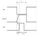
本発明の一態様において、前段信号がL信号からH信号に切り替わるまでの期間より、第1のクロック信号がH信号からL信号に切り替わってから第2のクロック信号がL信号からH信号に切り替わるまでの期間を長く取る液晶表示装置としてもよい。 In one embodiment of the present invention, the second clock signal is switched from the L signal to the H signal after the first clock signal is switched from the H signal to the L signal from the period until the previous stage signal is switched from the L signal to the H signal. It may be a liquid crystal display device that takes a long period of time.
本発明の一態様において、駆動回路は、制御回路、第1端子が第4信号線に電気的に接続され、第2端子が低電源電位を供給する配線に電気的に接続された第4トランジスタ、及び第1端子が第1トランジスタのゲートと第2トランジスタの第2端子と第3トランジスタの第2端子とが互いに電気的に接続されたノードに電気的に接続され、第2端子が低電源電位を供給する配線に電気的に接続された第5トランジスタと、を有し、制御回路は、第1トランジスタのゲートと第2トランジスタの第2端子と第3トランジスタの第2端子とが互いに電気的に接続されたノードの電位に応じて、第4トランジスタのゲート及び第5トランジスタのゲートの電位を制御する液晶表示装置としてもよい。 In one embodiment of the present invention, the driver circuit includes a control circuit, a fourth transistor in which the first terminal is electrically connected to the fourth signal line and the second terminal is electrically connected to the wiring that supplies the low power supply potential. And the first terminal is electrically connected to a node where the gate of the first transistor, the second terminal of the second transistor, and the second terminal of the third transistor are electrically connected to each other, and the second terminal is a low power supply. A fifth transistor electrically connected to a wiring for supplying a potential; and the control circuit includes a gate of the first transistor, a second terminal of the second transistor, and a second terminal of the third transistor electrically connected to each other. Alternatively, a liquid crystal display device may be used in which the potentials of the gates of the fourth transistor and the fifth transistor are controlled in accordance with the potentials of the connected nodes.
本発明の一態様において、第1トランジスタ乃至第5トランジスタは、同じ極性のトランジスタである液晶表示装置としてもよい。 In one embodiment of the present invention, the first transistor to the fifth transistor may be liquid crystal display devices that are transistors having the same polarity.
本発明の一態様において、奇数段のパルス出力回路の第1端子には第1のクロック信号、第2端子には第2のクロック信号が供給されており、偶数段のパルス出力回路の第1端子には第3のクロック信号、第2端子には第4のクロック信号が供給される液晶表示装置としてもよい。 In one embodiment of the present invention, the first clock signal is supplied to the first terminal of the odd-numbered pulse output circuit, and the second clock signal is supplied to the second terminal. A liquid crystal display device in which a third clock signal is supplied to the terminal and a fourth clock signal is supplied to the second terminal may be used.
なお、スイッチとしては、様々な形態のものを用いることができる。スイッチの一例としては、電気的スイッチ又は機械的なスイッチなどを用いることができる。つまり、スイッチは、電流を制御できるものであればよく、特定のものに限定されない。スイッチの一例としては、トランジスタ(例えば、バイポーラトランジスタ、MOSトランジスタなど)、ダイオード(例えば、PNダイオード、PINダイオード、ショットキーダイオード、MIM(Metal Insulator Metal)ダイオード、MIS(Metal Insulator Semiconductor)ダイオード、ダイオード接続のトランジスタなど)、又はこれらを組み合わせた論理回路などがある。機械的なスイッチの一例としては、デジタルマイクロミラーデバイス(DMD)のように、MEMS(マイクロ・エレクトロ・メカニカル・システム)技術を用いたスイッチがある。そのスイッチは、機械的に動かすことが可能な電極を有し、その電極が動くことによって、導通と非導通とを制御して動作する。 Note that various types of switches can be used as the switch. As an example of the switch, an electrical switch or a mechanical switch can be used. That is, the switch is not limited to a specific one as long as it can control the current. Examples of switches include transistors (eg, bipolar transistors, MOS transistors, etc.), diodes (eg, PN diodes, PIN diodes, Schottky diodes, MIM (Metal Insulator Metal) diodes, MIS (Metal Insulator Semiconductor) diodes, and diode connections. Or a logic circuit combining these transistors. An example of a mechanical switch is a switch using MEMS (micro electro mechanical system) technology, such as a digital micromirror device (DMD). The switch has an electrode that can be moved mechanically, and operates by controlling conduction and non-conduction by moving the electrode.
なお、スイッチとしてトランジスタを用いる場合、そのトランジスタは単なるスイッチとして動作するため、トランジスタの極性(導電型)は特に限定されない。 Note that in the case where a transistor is used as a switch, the transistor operates as a mere switch, and thus the polarity (conductivity type) of the transistor is not particularly limited.
なお、スイッチとして、Nチャネル型トランジスタとPチャネル型トランジスタとの両方を用いて、CMOS型のスイッチを用いてもよい。 Note that a CMOS switch may be used as the switch by using both an N-channel transistor and a P-channel transistor.
なお、表示素子、表示素子を有する装置である表示装置、発光素子、及び発光素子を有する装置である発光装置は、様々な形態を用いること、又は様々な素子を有することが出来る。表示素子、表示装置、発光素子又は発光装置の一例としては、EL(エレクトロルミネッセンス)素子(有機物及び無機物を含むEL素子、有機EL素子、無機EL素子)、LED(白色LED、赤色LED、緑色LED、青色LEDなど)、トランジスタ(電流に応じて発光するトランジスタ)、電子放出素子、液晶素子、電子インク、電気泳動素子、グレーティングライトバルブ(GLV)、プラズマディスプレイパネル(PDP)、デジタルマイクロミラーデバイス(DMD)、圧電セラミックディスプレイ、カーボンナノチューブ、など、電気磁気的作用により、コントラスト、輝度、反射率、透過率などが変化する表示媒体を有するものがある。EL素子を用いた表示装置の一例としては、ELディスプレイなどがある。電子放出素子を用いた表示装置の一例としては、フィールドエミッションディスプレイ(FED)又はSED方式平面型ディスプレイ(SED:Surface−conduction Electron−emitter Disply)などがある。液晶素子を用いた表示装置の一例としては、液晶ディスプレイ(透過型液晶ディスプレイ、半透過型液晶ディスプレイ、反射型液晶ディスプレイ、直視型液晶ディスプレイ、投射型液晶ディスプレイ)などがある。電子インク又は電気泳動素子を用いた表示装置の一例としては、電子ペーパーなどがある。 Note that a display element, a display device that is a device including a display element, a light-emitting element, and a light-emitting device that is a device including a light-emitting element can have various modes or have various elements. As an example of a display element, a display device, a light emitting element, or a light emitting device, an EL (electroluminescence) element (an EL element including an organic substance and an inorganic substance, an organic EL element, an inorganic EL element), an LED (white LED, red LED, green LED) , Blue LEDs, etc.), transistors (transistors that emit light in response to current), electron-emitting devices, liquid crystal devices, electronic ink, electrophoretic devices, grating light valves (GLV), plasma display panels (PDP), digital micromirror devices ( Some of them have display media whose contrast, brightness, reflectance, transmittance, and the like change due to an electromagnetic action, such as DMD), piezoelectric ceramic displays, and carbon nanotubes. An example of a display device using an EL element is an EL display. As an example of a display device using an electron-emitting device, there is a field emission display (FED), a SED type flat display (SED: Surface-conduction Electron-emitter Display), or the like. As an example of a display device using a liquid crystal element, there is a liquid crystal display (a transmissive liquid crystal display, a transflective liquid crystal display, a reflective liquid crystal display, a direct view liquid crystal display, a projection liquid crystal display) and the like. An example of a display device using electronic ink or an electrophoretic element is electronic paper.
液晶素子の一例としては、液晶の光学的変調作用によって光の透過又は非透過を制御する素子がある。その素子は一対の電極と液晶層により構造されることが可能である。なお、液晶の光学的変調作用は、液晶にかかる電界(横方向の電界、縦方向の電界又は斜め方向の電界を含む)によって制御される。なお、具体的には、液晶素子の一例としては、ネマチック液晶、コレステリック液晶、スメクチック液晶、ディスコチック液晶、サーモトロピック液晶、リオトロピック液晶、低分子液晶、高分子液晶、高分子分散型液晶(PDLC)、強誘電液晶、反強誘電液晶、主鎖型液晶、側鎖型高分子液晶、プラズマアドレス液晶(PALC)、バナナ型液晶などを挙げることができる。また、液晶の駆動方式としては、TN(Twisted Nematic)モード、STN(Super Twisted Nematic)モード、IPS(In−Plane−Switching)モード、FFS(Fringe Field Switching)モード、MVA(Multi−domain Vertical Alignment)モード、PVA(Patterned Vertical Alignment)モード、ASV(Advanced Super View)モード、ASM(Axially Symmetric aligned Micro−cell)モード、OCB(Optically Compensated Birefringence)モード、ECB(Electrically Controlled Birefringence)モード、FLC(Ferroelectric Liquid Crystal)モード、AFLC(AntiFerroelectric Liquid Crystal)モード、PDLC(Polymer Dispersed Liquid Crystal)モード、ゲストホストモード、ブルー相(Blue Phase)モードなどがある。ただし、これに限定されず、液晶素子及びその駆動方式として様々なものを用いることができる。 As an example of a liquid crystal element, there is an element that controls transmission or non-transmission of light by an optical modulation action of liquid crystal. The element can be structured by a pair of electrodes and a liquid crystal layer. Note that the optical modulation action of the liquid crystal is controlled by an electric field applied to the liquid crystal (including a horizontal electric field, a vertical electric field, or an oblique electric field). Specifically, examples of liquid crystal elements include nematic liquid crystals, cholesteric liquid crystals, smectic liquid crystals, discotic liquid crystals, thermotropic liquid crystals, lyotropic liquid crystals, low molecular liquid crystals, polymer liquid crystals, and polymer dispersed liquid crystals (PDLC). And ferroelectric liquid crystal, antiferroelectric liquid crystal, main chain liquid crystal, side chain polymer liquid crystal, plasma addressed liquid crystal (PALC), and banana liquid crystal. In addition, as a driving method of the liquid crystal, a TN (Twisted Nematic) mode, an STN (Super Twisted Nematic) mode, an IPS (In-Plane-Switching) mode, an FFS (Fringe Field Switching) mode, and an MVA (Multi-Antm Quantitative Alignment) are used. Mode, PVA (Patterned Vertical Alignment) mode, ASV (Advanced Super View) mode, ASM (Axial Symmetrically Coated MicroBell) mode, OCB (Optically Compensated BEC) mode Included birefringence mode, FLC (Ferroelectric Liquid Crystal) mode, AFLC (Antiferroelectric Liquid Crystal) mode, PDLC (Polymer Dispersed Liquid Crystal) mode, guest mode, B guest mode, guest mode. However, the present invention is not limited to this, and various liquid crystal elements and driving methods thereof can be used.
なお、トランジスタとして、様々な構造のトランジスタを用いることが出来る。よって、用いるトランジスタの種類に限定はない。トランジスタの一例としては、非晶質シリコン、多結晶シリコン、微結晶(マイクロクリスタル、ナノクリスタル、セミアモルファスとも言う)シリコンなどに代表される非単結晶半導体膜を有する薄膜トランジスタ(TFT)などを用いることが出来る。 Note that transistors with various structures can be used as the transistor. Thus, there is no limitation on the type of transistor used. As an example of a transistor, a thin film transistor (TFT) including a non-single-crystal semiconductor film typified by amorphous silicon, polycrystalline silicon, microcrystalline (also referred to as microcrystal, nanocrystal, or semi-amorphous) silicon is used. I can do it.
なお、トランジスタの一例としては、ZnO、a−InGaZnO、SiGe、GaAs、IZO、ITO、SnO、TiO、AlZnSnO(AZTO)などの化合物半導体又は酸化物半導体を有するトランジスタ又は、これらの化合物半導体又は酸化物半導体を薄膜化した薄膜トランジスタなどを用いることが出来る。これらにより、製造温度を低くできるので、例えば、室温でトランジスタを製造することが可能となる。その結果、耐熱性の低い基板、例えばプラスチック基板又はフィルム基板などに直接トランジスタを形成することが出来る。なお、これらの化合物半導体又は酸化物半導体を、トランジスタのチャネル部分に用いるだけでなく、それ以外の用途で用いることも出来る。例えば、これらの化合物半導体又は酸化物半導体を配線、抵抗素子、画素電極、又は透光性を有する電極などとして用いることができる。それらをトランジスタと同時に成膜又は形成することが可能なため、コストを低減できる。 Note that as an example of a transistor, a transistor including a compound semiconductor or an oxide semiconductor such as ZnO, a-InGaZnO, SiGe, GaAs, IZO, ITO, SnO, TiO, and AlZnSnO (AZTO), or a compound semiconductor or an oxide thereof. A thin film transistor obtained by thinning a semiconductor can be used. As a result, the manufacturing temperature can be lowered, so that the transistor can be manufactured at room temperature, for example. As a result, the transistor can be formed directly on a substrate having low heat resistance, such as a plastic substrate or a film substrate. Note that these compound semiconductors or oxide semiconductors can be used not only for a channel portion of a transistor but also for other purposes. For example, these compound semiconductors or oxide semiconductors can be used as a wiring, a resistance element, a pixel electrode, a light-transmitting electrode, or the like. Since these can be formed or formed simultaneously with the transistor, cost can be reduced.
なお、トランジスタの一例としては、インクジェット法又は印刷法を用いて形成したトランジスタなどを用いることが出来る。これらにより、室温で製造、低真空度で製造、又は大型基板上に製造することができる。よって、マスク(レチクル)を用いなくても製造することが可能となるため、トランジスタのレイアウトを容易に変更することが出来る。または、レジストを用いらずに製造することが可能なので、材料費が安くなり、工程数を削減できる。または、必要な部分にのみ膜を付けることが可能なので、全面に成膜した後でエッチングする、という製法よりも、材料が無駄にならず、低コストにできる。 Note that as an example of a transistor, a transistor formed using an inkjet method or a printing method can be used. By these, it can manufacture at room temperature, manufacture at a low vacuum degree, or can manufacture on a large sized board | substrate. Therefore, since the transistor can be manufactured without using a mask (reticle), the layout of the transistor can be easily changed. Alternatively, since it can be manufactured without using a resist, the material cost is reduced and the number of processes can be reduced. Alternatively, since a film can be formed only on a necessary portion, the material is not wasted and the cost can be reduced as compared with a manufacturing method in which etching is performed after film formation on the entire surface.
なお、トランジスタの一例としては、有機半導体やカーボンナノチューブを有するトランジスタ等を用いることができる。これらにより、曲げることが可能な基板上にトランジスタを形成することが出来る。このような基板を用いた半導体装置は、衝撃に強くすることができる。 Note that as an example of a transistor, a transistor including an organic semiconductor or a carbon nanotube can be used. Thus, a transistor can be formed over a substrate that can be bent. A semiconductor device using such a substrate can be resistant to impact.
なお、トランジスタとしては、他にも様々な構造のトランジスタを用いることができる。例えば、トランジスタとして、MOS型トランジスタ、接合型トランジスタ、バイポーラトランジスタなどを用いることが出来る。 Note that transistors having various structures can be used as the transistor. For example, a MOS transistor, a junction transistor, a bipolar transistor, or the like can be used as the transistor.
なお、トランジスタの一例としては、ゲート電極が2個以上のマルチゲート構造のトランジスタを用いることができる。マルチゲート構造にすると、チャネル領域が直列に接続されるため、複数のトランジスタが直列に接続された構造となる。 Note that as an example of a transistor, a multi-gate transistor having two or more gate electrodes can be used. When the multi-gate structure is used, the channel regions are connected in series, so that a plurality of transistors are connected in series.
なお、トランジスタの一例としては、チャネルの上下にゲート電極が配置されている構造のトランジスタを適用することができる。チャネルの上下にゲート電極が配置される構造にすることにより、複数のトランジスタが並列に接続されたような回路構成となる。 Note that as an example of a transistor, a transistor with a structure where gate electrodes are formed above and below a channel can be used. With a structure in which gate electrodes are arranged above and below a channel, a circuit configuration in which a plurality of transistors are connected in parallel is obtained.
なお、トランジスタの一例としては、チャネル領域の上にゲート電極が配置されている構造、チャネル領域の下にゲート電極が配置されている構造、正スタガ構造、逆スタガ構造、チャネル領域を複数の領域に分けた構造、チャネル領域を並列に接続した構造、又はチャネル領域が直列に接続する構造などのトランジスタを用いることができる。 Note that as an example of a transistor, a structure in which a gate electrode is disposed over a channel region, a structure in which a gate electrode is disposed under a channel region, a normal staggered structure, an inverted staggered structure, and a channel region in a plurality of regions Transistors having a structure divided into two, a structure in which channel regions are connected in parallel, or a structure in which channel regions are connected in series can be used.
なお、トランジスタの一例としては、チャネル領域(もしくはその一部)にソース電極やドレイン電極が重なっている構造のトランジスタを用いることができる。 Note that as an example of a transistor, a transistor with a structure in which a source electrode or a drain electrode overlaps with a channel region (or part thereof) can be used.
なお、トランジスタの一例としては、LDD領域を設けた構造のトランジスタを適用できる。 Note that as an example of a transistor, a transistor having an LDD region can be used.
なお、様々な基板を用いて、トランジスタを形成することが出来る。基板の種類は、特定のものに限定されることはない。その基板の一例としては、半導体基板(例えば単結晶基板又はシリコン基板)、SOI基板、ガラス基板、石英基板、プラスチック基板、金属基板、ステンレス・スチル基板、ステンレス・スチル・ホイルを有する基板、タングステン基板、タングステン・ホイルを有する基板、可撓性基板、貼り合わせフィルム、繊維状の材料を含む紙、又は基材フィルムなどがある。ガラス基板の一例としては、バリウムホウケイ酸ガラス、アルミノホウケイ酸ガラス、又はソーダライムガラスなどがある。可撓性基板の一例としては、ポリエチレンテレフタレート(PET)、ポリエチレンナフタレート(PEN)、ポリエーテルサルフォン(PES)に代表されるプラスチック、又はアクリル等の可撓性を有する合成樹脂などがある。貼り合わせフィルムの一例としては、ポリプロピレン、ポリエステル、ビニル、ポリフッ化ビニル、又は塩化ビニルなどがある。基材フィルムの一例としては、ポリエステル、ポリアミド、ポリイミド、無機蒸着フィルム、又は紙類などがある。 Note that a transistor can be formed using various substrates. The kind of board | substrate is not limited to a specific thing. Examples of the substrate include a semiconductor substrate (for example, a single crystal substrate or a silicon substrate), an SOI substrate, a glass substrate, a quartz substrate, a plastic substrate, a metal substrate, a stainless steel substrate, a substrate having stainless steel foil, and a tungsten substrate. , A substrate having a tungsten foil, a flexible substrate, a laminated film, a paper containing a fibrous material, or a base film. Examples of the glass substrate include barium borosilicate glass, aluminoborosilicate glass, and soda lime glass. As an example of the flexible substrate, there are plastics typified by polyethylene terephthalate (PET), polyethylene naphthalate (PEN), and polyethersulfone (PES), or a synthetic resin having flexibility such as acrylic. Examples of the laminated film include polypropylene, polyester, vinyl, polyvinyl fluoride, or vinyl chloride. Examples of the base film include polyester, polyamide, polyimide, an inorganic vapor deposition film, and papers.
なお、ある基板を用いてトランジスタを形成し、その後、別の基板にトランジスタを転置し、別の基板上にトランジスタを配置してもよい。トランジスタが転置される基板の一例としては、上述したトランジスタを形成することが可能な基板に加え、紙基板、セロファン基板、石材基板、木材基板、布基板(天然繊維(絹、綿、麻)、合成繊維(ナイロン、ポリウレタン、ポリエステル)若しくは再生繊維(アセテート、キュプラ、レーヨン、再生ポリエステル)などを含む)、皮革基板、又はゴム基板などがある。 Note that a transistor may be formed using a certain substrate, and then the transistor may be transferred to another substrate, and the transistor may be disposed on another substrate. As an example of the substrate on which the transistor is transferred, in addition to the substrate on which the transistor can be formed, a paper substrate, a cellophane substrate, a stone substrate, a wood substrate, a cloth substrate (natural fiber (silk, cotton, hemp), There are synthetic fibers (nylon, polyurethane, polyester) or recycled fibers (including acetate, cupra, rayon, recycled polyester), leather substrates, rubber substrates, and the like.
なお、所定の機能を実現させるために必要な回路の全てを、同一の基板(例えば、ガラス基板、プラスチック基板、単結晶基板、又はSOI基板など)に形成することが可能である。こうして、部品点数の削減によるコストの低減、又は回路部品との接続点数の低減による信頼性の向上を図ることができる。 Note that all circuits necessary for realizing a predetermined function can be formed over the same substrate (eg, a glass substrate, a plastic substrate, a single crystal substrate, or an SOI substrate). Thus, the cost can be reduced by reducing the number of components, or the reliability can be improved by reducing the number of connection points with circuit components.
なお、所定の機能を実現させるために必要な回路の全てを同じ基板に形成しないことが可能である。つまり、所定の機能を実現させるために必要な回路の一部は、ある基板に形成され、所定の機能を実現させるために必要な回路の別の一部は、別の基板に形成されていることが可能である。例えば、所定の機能を実現させるために必要な回路の一部は、ガラス基板に形成され、所定の機能を実現させるために必要な回路の別の一部は、単結晶基板(又はSOI基板)に形成されることが可能である。そして、所定の機能を実現させるために必要な回路の別の一部が形成される単結晶基板(ICチップともいう)を、COG(Chip On Glass)によって、ガラス基板に接続して、ガラス基板にそのICチップを配置することが可能である。または、ICチップを、TAB(Tape Automated Bonding)、COF(Chip On Film)、SMT(Surface Mount Technology)、又はプリント基板などを用いてガラス基板と接続することが可能である。 Note that it is possible not to form all the circuits necessary for realizing a predetermined function on the same substrate. In other words, a part of the circuit necessary for realizing the predetermined function is formed on a certain substrate, and another part of the circuit necessary for realizing the predetermined function is formed on another substrate. It is possible. For example, a part of a circuit necessary for realizing a predetermined function is formed on a glass substrate, and another part of a circuit required for realizing a predetermined function is a single crystal substrate (or an SOI substrate). Can be formed. Then, a single crystal substrate (also referred to as an IC chip) on which another part of a circuit necessary for realizing a predetermined function is formed is connected to the glass substrate by COG (Chip On Glass), and the glass substrate It is possible to arrange the IC chip. Alternatively, the IC chip can be connected to the glass substrate using TAB (Tape Automated Bonding), COF (Chip On Film), SMT (Surface Mount Technology), or a printed circuit board.
なお、トランジスタとは、ゲートと、ドレインと、ソースとを含む少なくとも三つの端子を有する素子であり、ドレイン領域とソース領域の間にチャネル領域を有しており、ドレイン領域とチャネル領域とソース領域とを介して電流を流すことが出来るものである。ここで、ソースとドレインとは、トランジスタの構造又は動作条件等によって変わるため、いずれがソースまたはドレインであるかを限定することが困難である。そこで、ソースとして機能する領域、及びドレインとして機能する領域を、ソース又はドレインと呼ばない場合がある。その場合、一例として、ソースとドレインとの一方を、第1端子、第1電極、又は第1領域と表記し、ソースとドレインとの他方を、第2端子、第2電極、又は第2領域と表記する場合がある。 Note that a transistor is an element having at least three terminals including a gate, a drain, and a source. The transistor has a channel region between the drain region and the source region, and the drain region, the channel region, and the source region. A current can be passed through the. Here, since the source and the drain vary depending on the structure or operating conditions of the transistor, it is difficult to limit which is the source or the drain. Thus, a region functioning as a source and a region functioning as a drain may not be referred to as a source or a drain. In that case, as an example, one of the source and the drain is referred to as a first terminal, a first electrode, or a first region, and the other of the source and the drain is referred to as a second terminal, a second electrode, or a second region. May be written.
なお、トランジスタは、ベースとエミッタとコレクタとを含む少なくとも三つの端子を有する素子であってもよい。この場合も同様に、一例として、エミッタとコレクタとの一方を、第1端子、第1電極、又は第1領域と表記し、エミッタとコレクタとの他方を、第2端子、第2電極、又は第2領域と表記する場合がある。なお、トランジスタとしてバイポーラトランジスタが用いられる場合、ゲートという表記をベースと言い換えることが可能である。 Note that the transistor may be an element having at least three terminals including a base, an emitter, and a collector. Similarly, in this case, as an example, one of the emitter and the collector is represented as a first terminal, a first electrode, or a first region, and the other of the emitter and the collector is represented as a second terminal, a second electrode, or Sometimes referred to as a second region. Note that in the case where a bipolar transistor is used as the transistor, the term gate can be referred to as the base.
なお、AとBとが接続されている、と明示的に記載する場合は、AとBとが電気的に接続されている場合と、AとBとが機能的に接続されている場合と、AとBとが直接接続されている場合とを含むものとする。ここで、A、Bは、対象物(例えば、装置、素子、回路、配線、電極、端子、導電膜、層、など)であるとする。したがって、所定の接続関係、例えば、図または文章に示された接続関係に限定されず、図または文章に示された接続関係以外のものも含むものとする。 In addition, when it is explicitly described that A and B are connected, A and B are electrically connected, and A and B are functionally connected. , A and B are directly connected. Here, A and B are objects (for example, devices, elements, circuits, wirings, electrodes, terminals, conductive films, layers, etc.). Therefore, it is not limited to a predetermined connection relationship, for example, the connection relationship shown in the figure or text, and includes things other than the connection relation shown in the figure or text.
AとBとが電気的に接続されている場合の一例としては、AとBとの電気的な接続を可能とする素子(例えば、スイッチ、トランジスタ、容量素子、インダクタ、抵抗素子、ダイオードなど)が、AとBとの間に1個以上接続されることが可能である。 An example of the case where A and B are electrically connected is an element that enables electrical connection between A and B (for example, a switch, a transistor, a capacitor, an inductor, a resistor, a diode, etc.) Can be connected one or more between A and B.
AとBとが機能的に接続されている場合の一例としては、AとBとの機能的な接続を可能とする回路(例えば、論理回路(インバータ、NAND回路、NOR回路など)、信号変換回路(DA変換回路、AD変換回路、ガンマ補正回路など)、電位レベル変換回路(電源回路(昇圧回路、降圧回路など)、信号の電位レベルを変えるレベルシフタ回路など)、電圧源、電流源、切り替え回路、増幅回路(信号振幅または電流量などを大きく出来る回路、オペアンプ、差動増幅回路、ソースフォロワ回路、バッファ回路など)、信号生成回路、記憶回路、制御回路など)が、AとBとの間に1個以上接続されることが可能である。なお、一例として、AとBとの間に別の回路を挟んでいても、Aから出力された信号がBへ伝達される場合は、AとBとは機能的に接続されているものとする。 As an example of the case where A and B are functionally connected, a circuit (for example, a logic circuit (an inverter, a NAND circuit, a NOR circuit, etc.) that enables functional connection between A and B, signal conversion, etc. Circuit (DA conversion circuit, AD conversion circuit, gamma correction circuit, etc.), potential level conversion circuit (power supply circuit (boost circuit, step-down circuit, etc.), level shifter circuit that changes signal potential level, etc.), voltage source, current source, switching Circuit, amplifier circuit (circuit that can increase signal amplitude or current amount, operational amplifier, differential amplifier circuit, source follower circuit, buffer circuit, etc.), signal generation circuit, memory circuit, control circuit, etc.) One or more can be connected between them. As an example, if a signal output from A is transmitted to B even if another circuit is interposed between A and B, A and B are functionally connected. To do.
なお、AとBとが電気的に接続されている、と明示的に記載する場合は、AとBとが電気的に接続されている場合(つまり、AとBとの間に別の素子又は別の回路を挟んで接続されている場合)と、AとBとが機能的に接続されている場合(つまり、AとBとの間に別の回路を挟んで機能的に接続されている場合)と、AとBとが直接接続されている場合(つまり、AとBとの間に別の素子又は別の回路を挟まずに接続されている場合)とを含むものとする。つまり、電気的に接続されている、と明示的に記載する場合は、単に、接続されている、とのみ明示的に記載されている場合と同じであるとする。 Note that in the case where it is explicitly described that A and B are electrically connected, another element is connected between A and B (that is, between A and B). Or when A and B are functionally connected (that is, they are functionally connected with another circuit between A and B). And a case where A and B are directly connected (that is, a case where another element or another circuit is not connected between A and B). That is, when it is explicitly described that it is electrically connected, it is the same as when it is explicitly only described that it is connected.
なお、Aの上にBが形成されている、あるいは、A上にBが形成されている、と明示的に記載する場合は、Aの上にBが直接接して形成されていることに限定されない。直接接してはいない場合、つまり、AとBと間に別の対象物が介在する場合も含むものとする。ここで、A、Bは、対象物(例えば、装置、素子、回路、配線、電極、端子、導電膜、層、など)であるとする。 In addition, when it is explicitly described that B is formed on A or B is formed on A, it is limited that B is formed in direct contact with A. Not. The case where it is not in direct contact, that is, the case where another object is interposed between A and B is also included. Here, A and B are objects (for example, devices, elements, circuits, wirings, electrodes, terminals, conductive films, layers, etc.).
従って例えば、層Aの上に(もしくは層A上に)、層Bが形成されている、と明示的に記載されている場合は、層Aの上に直接接して層Bが形成されている場合と、層Aの上に直接接して別の層(例えば層Cや層Dなど)が形成されていて、その上に直接接して層Bが形成されている場合とを含むものとする。なお、別の層(例えば層Cや層Dなど)は、単層でもよいし、複層でもよい。 Therefore, for example, when it is explicitly described that the layer B is formed on the layer A (or on the layer A), the layer B is formed in direct contact with the layer A. And the case where another layer (for example, layer C or layer D) is formed in direct contact with the layer A, and the layer B is formed in direct contact therewith. Note that another layer (for example, the layer C or the layer D) may be a single layer or a multilayer.
さらに、Aの上方にBが形成されている、と明示的に記載されている場合についても同様であり、Aの上にBが直接接していることに限定されず、AとBとの間に別の対象物が介在する場合も含むものとする。従って例えば、層Aの上方に、層Bが形成されている、という場合は、層Aの上に直接接して層Bが形成されている場合と、層Aの上に直接接して別の層(例えば層Cや層Dなど)が形成されていて、その上に直接接して層Bが形成されている場合とを含むものとする。なお、別の層(例えば層Cや層Dなど)は、単層でもよいし、複層でもよい。 Furthermore, the same applies to the case where B is explicitly described as being formed above A, and is not limited to the direct contact of B on A. This includes the case where another object is interposed in. Therefore, for example, when the layer B is formed above the layer A, the case where the layer B is formed in direct contact with the layer A and the case where another layer is formed in direct contact with the layer A. (For example, the layer C or the layer D) is formed, and the layer B is formed in direct contact therewith. Note that another layer (for example, the layer C or the layer D) may be a single layer or a multilayer.
なお、Aの上にBが形成されている、A上にBが形成されている、又はAの上方にBが形成されている、と明示的に記載する場合、斜め上にBが形成される場合も含むこととする。 Note that when B is formed on A, B is formed on A, or B is formed above A, B is formed obliquely above. This is included.
なお、Aの下にBが、あるいは、Aの下方にBが、の場合についても、同様である。 The same applies to the case where B is below A or B is below A.
なお、明示的に単数として記載されているものについては、単数であることが望ましい。ただし、これに限定されず、複数であることも可能である。同様に、明示的に複数として記載されているものについては、複数であることが望ましい。ただし、これに限定されず、単数であることも可能である。 In addition, about what is explicitly described as singular, it is preferable that it is singular. However, the present invention is not limited to this, and a plurality of them is also possible. Similarly, a plurality that is explicitly described as a plurality is preferably a plurality. However, the present invention is not limited to this, and the number can be singular.
なお、図において、大きさ、層の厚さ、又は領域は、明瞭化のために誇張されている場合がある。よって、必ずしもそのスケールに限定されない。 Note that the size, the thickness of layers, or regions in drawings is sometimes exaggerated for simplicity. Therefore, it is not necessarily limited to the scale.
なお、図は、理想的な例を模式的に示したものであり、図に示す形状又は値などに限定されない。例えば、製造技術による形状のばらつき、誤差による形状のばらつき、ノイズによる信号、電圧、若しくは電流のばらつき、又は、タイミングのずれによる信号、電圧、若しくは電流のばらつきなどを含むことが可能である。 The figure schematically shows an ideal example, and is not limited to the shape or value shown in the figure. For example, variation in shape due to manufacturing technology, variation in shape due to error, variation in signal, voltage, or current due to noise, variation in signal, voltage, or current due to timing shift, and the like can be included.
なお、専門用語は、特定の実施の形態、又は実施例などを述べる目的で用いられる場合が多い。ただし、本発明の一態様は、専門用語によって、限定して解釈されるものではない。 Technical terms are often used for the purpose of describing specific embodiments or examples. Note that one embodiment of the present invention is not construed as being limited by technical terms.
なお、定義されていない文言(専門用語又は学術用語などの科学技術文言を含む)は、通常の当業者が理解する一般的な意味と同等の意味として用いることが可能である。辞書等により定義されている文言は、関連技術の背景と矛盾がないような意味に解釈されることが好ましい。 Note that undefined words (including scientific and technical terms such as technical terms or academic terms) can be used as meanings equivalent to general meanings understood by those skilled in the art. Words defined by a dictionary or the like are preferably interpreted in a meaning that is consistent with the background of related technology.
なお、第1、第2、第3などの語句は、様々な要素、部材、領域、層、区域を他のものと区別して記述するために用いられる。よって、第1、第2、第3などの語句は、要素、部材、領域、層、区域などの数を限定するものではない。さらに、例えば、「第1の」を「第2の」又は「第3の」などと置き換えることが可能である。 Note that terms such as first, second, and third are used to distinguish various elements, members, regions, layers, and areas from others. Thus, the terms such as “first”, “second”, and “third” do not limit the number of elements, members, regions, layers, areas, and the like. Furthermore, for example, “first” can be replaced with “second” or “third”.
なお、「上に」、「上方に」、「下に」、「下方に」、「横に」、「右に」、「左に」、「斜めに」、「奥に」、「手前に」、「内に」、「外に」、又は「中に」などの空間的配置を示す語句は、ある要素又は特徴と、他の要素又は特徴との関連を、図によって簡単に示すために用いられる場合が多い。ただし、これに限定されず、これらの空間的配置を示す語句は、図に描く方向に加えて、他の方向を含むことが可能である。例えば、Aの上にB、と明示的に示される場合は、BがAの上にあることに限定されない。図中のデバイスは反転、又は180°回転することが可能なので、BがAの下にあることを含むことが可能である。このように、「上に」という語句は、「上に」の方向に加え、「下に」の方向を含むことが可能である。ただし、これに限定されず、図中のデバイスは様々な方向に回転することが可能なので、「上に」という語句は、「上に」、及び「下に」の方向に加え、「横に」、「右に」、「左に」、「斜めに」、「奥に」、「手前に」、「内に」、「外に」、又は「中に」などの他の方向を含むことが可能である。つまり、状況に応じて適切に解釈することが可能である。 “Up”, “Up”, “Down”, “Down”, “Landscape”, “Right”, “Left”, “Slanting”, “Back”, “Front” ”,“ In ”,“ out ”, or“ in ”terms that indicate spatial arrangements are used to briefly show the relationship between one element or feature and another element or feature by a diagram. Often used. However, the present invention is not limited to this, and the phrase indicating these spatial arrangements can include other directions in addition to the direction depicted in the drawing. For example, if B is explicitly indicated above A, then B is not limited to being above A. Since the device in the figure can be reversed or rotated 180 °, it can include B under A. Thus, the phrase “up” can include a “down” direction in addition to a “up” direction. However, the present invention is not limited to this, and the device in the figure can be rotated in various directions. Therefore, the phrase “up” is added to the directions of “up” and “down” and “sideways”. ”,“ Right ”,“ left ”,“ oblique ”,“ back ”,“ front ”,“ in ”,“ out ”, or“ in ” Is possible. That is, it is possible to interpret appropriately according to the situation.
本発明の一態様は、回路の誤動作を低減することで、表示品質の向上を図ることができる。または、本発明の一態様は、信号のなまり又は遅延を低減することができる。または本発明の一態様は、トランジスタの特性劣化を抑制することができる。または、本発明の一態様は、トランジスタのチャネル幅を小さくすることができる。または、本発明の一態様は、レイアウト面積を小さくすることができる。または、本発明の一態様は、表示装置の額縁を狭くすることができる。または、本発明の一態様は、表示装置を高精細にすることができる。または、本発明の一態様は、コストを低減することができる。 According to one embodiment of the present invention, display quality can be improved by reducing malfunction of a circuit. Alternatively, according to one embodiment of the present invention, signal rounding or delay can be reduced. Alternatively, according to one embodiment of the present invention, deterioration in characteristics of a transistor can be suppressed. Alternatively, according to one embodiment of the present invention, the channel width of a transistor can be reduced. Alternatively, according to one embodiment of the present invention, the layout area can be reduced. Alternatively, according to one embodiment of the present invention, a frame of a display device can be narrowed. Alternatively, according to one embodiment of the present invention, a display device can have high definition. Alternatively, according to one embodiment of the present invention, cost can be reduced.
以下、本発明の実施の形態について図面を参照しながら説明する。但し、実施の形態は多くの異なる態様で実施することが可能であり、趣旨及びその範囲から逸脱することなくその形態及び詳細を様々に変更し得ることは当業者であれば容易に理解される。従って実施の形態の記載内容に限定して解釈されるものではない。なお、以下に説明する構成において、同一部分又は同様な機能を有する部分は異なる図面間で共通の符号を用いて示し、同一部分又は同様な機能を有する部分の詳細な説明は省略する。 Hereinafter, embodiments of the present invention will be described with reference to the drawings. However, the embodiments can be implemented in many different modes, and it is easily understood by those skilled in the art that the modes and details can be variously changed without departing from the spirit and scope thereof. . Therefore, the present invention is not construed as being limited to the description of the embodiments. Note that in the structures described below, the same portions or portions having similar functions are denoted by the same reference numerals in different drawings, and detailed description of the same portions or portions having similar functions is omitted.
なお、ある一つの実施の形態の中で述べる内容(一部の内容でもよい)は、その実施の形態で述べる別の内容(一部の内容でもよい)、及び/又は、一つ若しくは複数の別の実施の形態で述べる内容(一部の内容でもよい)に対して、適用、組み合わせ、又は置き換えなどを行うことが出来る。 Note that the content (may be a part of content) described in one embodiment is different from the content (may be a part of content) described in the embodiment and / or one or more Application, combination, replacement, or the like can be performed on the content described in another embodiment (or part of the content).
なお、実施の形態の中で述べる内容とは、各々の実施の形態において、様々な図を用いて述べる内容、又は明細書に記載される文章を用いて述べる内容のことである。 Note that the contents described in the embodiments are contents described using various drawings or contents described in the specification in each embodiment.
なお、ある一つの実施の形態において述べる図(一部でもよい)は、その図の別の部分、その実施の形態において述べる別の図(一部でもよい)、及び/又は、一つ若しくは複数の別の実施の形態において述べる図(一部でもよい)に対して、組み合わせることにより、さらに多くの図を構成させることが出来る。 Note that a drawing (or a part thereof) described in one embodiment may be another part of the drawing, another drawing (may be a part) described in the embodiment, and / or one or more. More diagrams can be formed by combining the diagrams (may be a part) described in another embodiment.
(実施の形態1)
本実施の形態では、半導体装置の一例について説明する。本実施の形態の半導体装置は、一例として、シフトレジスタ、ゲートドライバ、ソースドライバ、又は表示装置などに用いることが可能である。なお、本実施の形態の半導体装置を駆動回路と示すことが可能である。
(Embodiment 1)
In this embodiment, an example of a semiconductor device is described. For example, the semiconductor device of this embodiment can be used for a shift register, a gate driver, a source driver, a display device, or the like. Note that the semiconductor device of this embodiment can be referred to as a driver circuit.
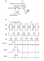
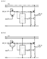
まず、駆動回路のシフトレジスタとして機能する半導体装置について、図1乃至図6を参照して説明する。半導体装置100は、第1のパルス出力回路101_1乃至第Nのパルス出力回路101_N(N≧2)を有している(図1(A)参照)。図1(A)に示す半導体装置100の第1のパルス出力回路101_1乃至第Nのパルス出力回路101_Nの各段には、第1の配線102より第1のクロック信号CK1、第2の配線103より第3のクロック信号CK3、第3の配線104より第2のクロック信号CK2、第4の配線105より第4のクロック信号CK4が入力される。また各段のパルス出力回路には、スタートパルスSPまたは一段前のパルス出力回路からの出力信号(前段信号OUT_N−1ともいう)が入力される。また各段のパルス出力回路からは、ゲート線またはデータ線等に出力するための出力信号OUT_Nが出力される。なお、パルス出力回路は、表示部の表示に寄与しない信号を出力するダミーの段を設けてもよく、例えばゲートドライバのシフトレジスタに用いられ、n本のゲート線に順次パルスを出力する構成では、n≦Nの段数とする構成とすればよい。なお、出力信号の出力数は、出力される先の負荷に応じて複数設ける構成としてもよい。負荷に応じた複数の出力信号を出力する構成とすることで、信号のなまり又は遅延等を低減することができる。
First, a semiconductor device functioning as a shift register of a driver circuit is described with reference to FIGS. The
なお第3のクロック信号CK3は、一例として、第1のクロック信号CK1から180°位相がずれた信号である。また、第1のクロック信号CK1はデューティ比50%の信号であるとし、第3のクロック信号CK3は、第1のクロック信号CK1の反転クロック信号でもよい。なお第4のクロック信号CK4は、一例として、第2のクロック信号CK2から180°位相がずれた信号である。 Note that the third clock signal CK3 is, for example, a signal that is 180 ° out of phase with the first clock signal CK1. Further, the first clock signal CK1 may be a signal having a duty ratio of 50%, and the third clock signal CK3 may be an inverted clock signal of the first clock signal CK1. Note that the fourth clock signal CK4 is, for example, a signal that is 180 degrees out of phase with the second clock signal CK2.
なお、第1のクロック信号CK1及び第3のクロック信号CK3、並びに第2のクロック信号CK2及び第4のクロック信号CK4は、奇数段のパルス出力回路と偶数段のパルス出力回路では、入力される信号が入れ替わる。具体的には、図1(B)に示すように奇数段(ここでは一例として一段目)のパルス出力回路101_1において、第1端子に第1のクロック信号CK1が入力され、第2端子に第2のクロック信号CK2が入力され、第3端子にスタートパルスSP(3段目以降の奇数段では、前段信号OUT_N−1)が入力され、第4端子から出力信号OUT_Nが出力される。また、図1(C)に示すように偶数段(ここでは一例として二段目)のパルス出力回路101_2において、第1端子に第3のクロック信号CK3が入力され、第2端子に第4のクロック信号CK4が入力され、第3端子に前段信号OUT_1(4段目以降の偶数段では、前段信号OUT_N−1)が入力され、第4端子から出力信号OUT_2が出力される。なお第1のクロック信号CK1及び第3のクロック信号CK3、並びに第2のクロック信号CK2及び第4のクロック信号CK4は、一定の間隔でH信号(高電源電位レベル、Hレベルともいう)とL信号(低電源電位レベル、Lレベルともいう)を繰り返す信号とする。
Note that the first clock signal CK1 and the third clock signal CK3, and the second clock signal CK2 and the fourth clock signal CK4 are input in the odd-numbered pulse output circuit and the even-numbered pulse output circuit. Signals are switched. Specifically, as shown in FIG. 1B, in the odd-numbered pulse output circuit 101_1 (here, the first stage as an example), the first clock signal CK1 is input to the first terminal, and the
次にパルス出力回路の回路構成の一例について、図1(D)で説明する。なお図1(D)では、一例として、奇数段のパルス出力回路について構成について説明する。なお、奇数段と偶数段のパルス出力回路の違いについては、上述のように、第1のクロック信号CK1及び第3のクロック信号CK3、または第2のクロック信号CK2及び第4のクロック信号CK4のように入力される信号が入れ替わる点にある。 Next, an example of a circuit configuration of the pulse output circuit is described with reference to FIG. Note that in FIG. 1D, the structure of an odd-numbered pulse output circuit is described as an example. Note that the difference between the odd-numbered and even-numbered pulse output circuits is that the first clock signal CK1 and the third clock signal CK3, or the second clock signal CK2 and the fourth clock signal CK4, as described above. Thus, the input signals are interchanged.
パルス出力回路は、第1トランジスタ111乃至第5トランジスタ115、及び制御回路131を有している。また図1(D)では、上述した第1端子乃至第4端子に入力される信号に加え、第1電源線141より高電源電位VDD、第2電源線142より低電源電位VSSが供給される点について示している。なお図1(D)において、第1端子に第1のクロック信号CK1を入力する配線を第1信号線151、第2端子に第2のクロック信号CK2を入力する配線を第2信号線152、第3端子に前段信号OUT_N−1を入力する配線を第3信号線153、第4端子に出力信号OUT_Nを出力する配線を第4信号線154という。なお説明の上で、図1(D)に示すように、第1トランジスタ111のゲート、第2トランジスタ112の第2端子、第3トランジスタ113の第2端子、及び第5トランジスタ115の第1端子の接続箇所をノードA(nodeA)とする。また、第4トランジスタ114のゲート、第5トランジスタ115のゲートの接続箇所をノードB(nodeB)とする。
The pulse output circuit includes a
第1トランジスタ111は、第1端子が第1信号線151に接続され、第2端子が第4トランジスタ114の第1端子、及び第4信号線154に接続され、ゲートがノードAに接続されている。第2トランジスタ112は、第1端子が第2トランジスタ112のゲート、第3トランジスタ113の第1端子、及び第3信号線153に接続され、第2端子がノードAに接続され、ゲートが第2トランジスタ112の第1端子、第3トランジスタ113の第1端子、及び第3信号線153に接続されている。第3のトランジスタ113は、第1端子が第2トランジスタ112のゲート、第2トランジスタ112の第1端子、及び第3信号線153に接続され、第2端子がノードAに接続され、ゲートが第2信号線152に接続されている。第4のトランジスタ114は、第1端子が第1トランジスタ111の第2端子、及び第4信号線154に接続され、第2端子が第2電源線142に接続され、ゲートがノードBに接続されている。第5のトランジスタ115は、第1端子がノードAに接続され、第2端子が第2電源線142に接続され、ゲートがノードBに接続されている。制御回路131は、ノードAの電位に応じて、ノードBの電位の高低を制御する機能を有する回路であり、ノードA、第1電源線141、第2電源線142、ノードBに接続されている。
The
なお第1トランジスタ111のゲートと第2端子との間には、第1トランジスタ111のゲートを浮遊状態とすることによりブートストラップ動作を行うための容量素子を別途設けても良い。第1トランジスタ111のゲートと第2端子との間にある寄生容量でブートストラップ動作を行うことができれば、削減することもできる。
Note that a capacitor for performing a bootstrap operation may be separately provided between the gate of the
なお、電圧とは、グランド電位との電位差のことを示す場合が多い。よって、電圧、電位、電位差を置き換えて表記することができる。 Note that the voltage often indicates a potential difference from a ground potential. Therefore, voltage, potential, and potential difference can be replaced and expressed.
なお、第1のトランジスタ111乃至第5のトランジスタ115は、同じ極性であることが好ましく、Nチャネル型である場合が多い。ただし、これに限定されず、第1のトランジスタ111乃至第5のトランジスタ115は、Pチャネル型であることが可能である。
Note that the
ここで、本実施の形態で述べる回路動作について詳述する前に、比較例として、上記示した特許文献1に記載の回路構成の動作について説明し、本実施の形態で述べる構成の利点について詳述することにする。なお図28乃至図32で説明する比較例は、図1(A)乃至(D)に示す構成と比較するものであって、本明細書で開示する構成の全てと比較するものではないことを付記する。
Before describing the circuit operation described in this embodiment in detail, the operation of the circuit configuration described in
図28(A)には、特許文献1の図5、図6で説明のあるシフトレジスタを構成するトランジスタM1乃至M8について示している。特許文献1に記載の回路構成は、図28(B)に示すようにタイミングチャートに基づいて、ゲートドライバの出力信号OUT_Nの立ち下がり時間を短くすることができる。次に、図28(B)について、第1の期間T1、第2の期間T2、第3の期間T3、第4の期間T4、第5の期間T5に分けて、各トランジスタのオン又はオフ、及び各配線での電位について、説明する。なお各配線の電位は、簡略的に「H」(高電源電位に基づく信号、H信号)、「L」(低電源電位に基づく信号、L信号)として説明するものとする。なお図28(C)は、クロック信号CKと出力信号OUT_Nの波形について、特許文献1の図8と同様に、具体的に示したものである。なお図28(A)乃至(C)の記載は、特許文献1の図6乃至図8の記載と同様であるため、詳しい説明について特許文献1を援用するものとする。なお図28(A)の点線280で囲った領域のトランジスタM3、M5、M8は、ノードA(nodeA)の電位に応じて、ノードB(nodeB)の電位の高低を制御する機能を有する制御回路に相当し、トランジスタM4の導通または非導通を制御するものである。なお当該制御回路は、本実施の形態1の図1で説明する制御回路131と同等の機能を有する回路である。
FIG. 28A shows the transistors M1 to M8 included in the shift register described in FIGS. The circuit configuration described in
第1の期間T1において、まず前半の動作について図29(A)に期間T1−1として示す。なお、ここでいう「前半」とは、第1の期間T1に所定の電位が供給されることによる過渡期のことをいう。まず、前段信号OUT_N−1がH信号、クロック信号CKがL信号、リセットするための信号OUT_N+2(以下、リセット信号)がL信号となる。その結果、ノードAが低電源電位VSSにしきい値電圧分の電圧を加えた値(VSS+Vth)になり、図示するようにトランジスタM1、M3が導通する(図中、無印のトランジスタ)。また図29(A)に図示するように他のトランジスタM5、M7、M8は導通し、トランジスタM2、M4、M6は非導通となる(図中、X印のトランジスタ)。そして、図29(A)中の点線矢印のように電流が流れる。次に、第1の期間T1の後半の動作として期間T1−2を図29(B)に示す。なお、ここでいう「後半」とは、第1の期間T1に所定の電位が供給されることによって過渡期の状態を経た後の定常状態となった期間のことをいう。図29(A)のように電流が流れることで、ノードAの電位が高電源電位VDDからしきい値電圧分の電圧を引いた値(VDD−Vth)まで上昇し、図29(B)に示すようにトランジスタM7が非導通となる。このときノードAは浮遊状態となる。そして第1の期間T1での各配線の電位が図28(B)のように確定する。 In the first period T1, the operation in the first half is shown as a period T1-1 in FIG. Note that the “first half” here refers to a transition period due to a predetermined potential being supplied in the first period T1. First, the previous stage signal OUT_N-1 is an H signal, the clock signal CK is an L signal, and a reset signal OUT_N + 2 (hereinafter, a reset signal) is an L signal. As a result, the node A has a value (VSS + Vth) obtained by adding a voltage corresponding to the threshold voltage to the low power supply potential VSS, and the transistors M1 and M3 are turned on as illustrated (transistors not marked in the drawing). In addition, as shown in FIG. 29A, the other transistors M5, M7, and M8 are turned on, and the transistors M2, M4, and M6 are turned off (the transistors indicated by X in the figure). Then, a current flows as indicated by a dotted arrow in FIG. Next, FIG. 29B illustrates a period T1-2 as an operation in the second half of the first period T1. Note that the “second half” here refers to a period in which a predetermined potential is supplied in the first period T1 and a steady state is obtained after a transitional state. As a current flows as shown in FIG. 29A, the potential of the node A rises to a value (VDD−Vth) obtained by subtracting the voltage corresponding to the threshold voltage from the high power supply potential VDD, and FIG. As shown, transistor M7 is non-conductive. At this time, the node A is in a floating state. Then, the potential of each wiring in the first period T1 is determined as illustrated in FIG.
なお、図28(B)では、図28(C)に示すように、前段信号OUT_N−1となる別の段の出力信号OUT_Nがクロック信号CKの立ち上がりに比べ遅延する波形を簡略的に示している。前段信号OUT_N−1の遅延は、ノードAの電位の上昇、ノードBの電位の下降にも反映されることとなる。これはトランジスタM1の後段に接続される配線等の負荷が増大することによりトランジスタサイズを大きく設計することによるものである。そのため、トランジスタM1のゲート容量が増大し、トランジスタM1が導通状態または非導通状態に切り替わる際、トランジスタM1のゲートへの電荷の充電または放電にかかる時間が長くなり、これが信号の立ち上がりまたは立ち下がりの遅延として現れることとなる(図28(B)中の二点鎖線281)。ただし、この信号の立ち上がりまたは立ち下がりの遅延による、第1の期間T1での回路の誤動作はおこりにくい。
Note that in FIG. 28B, as illustrated in FIG. 28C, a waveform in which the output signal OUT_N of another stage that is the previous stage signal OUT_N−1 is delayed as compared with the rising edge of the clock signal CK is illustrated in a simplified manner. Yes. The delay of the pre-stage signal OUT_N−1 is also reflected in the increase in the potential of the node A and the decrease in the potential of the node B. This is because the transistor size is designed to be large by increasing the load such as wiring connected to the subsequent stage of the transistor M1. Therefore, when the gate capacitance of the transistor M1 is increased and the transistor M1 is switched to a conductive state or a non-conductive state, it takes a long time to charge or discharge the charge to the gate of the transistor M1, and this increases or decreases the signal. It appears as a delay (two-
次に第2の期間T2において、クロック信号CKがH信号となり、前段信号OUT_N−1、及びリセット信号OUT_N+2がL信号となる。その結果、出力信号OUT_Nの電位は上昇し、ブートストラップ動作によって浮遊状態になるノードAの電位が上昇し、図30(A)中の点線矢印のように電流が流れ、出力信号OUT_NがH信号を出力することとなる。 Next, in the second period T2, the clock signal CK becomes an H signal, and the preceding signal OUT_N−1 and the reset signal OUT_N + 2 become an L signal. As a result, the potential of the output signal OUT_N is increased, the potential of the node A that is in a floating state by the bootstrap operation is increased, a current flows as indicated by a dotted arrow in FIG. 30A, and the output signal OUT_N is changed to the H signal. Will be output.
次に第3の期間T3において、クロック信号CK、前段信号OUT_N−1、及びリセット信号OUT_N+2がL信号となる。このとき、ノードAの電位は第2の期間T2でのブートストラップ動作により(VDD+Vth)よりも高い値になっているので、トランジスタM1は導通状態のままとなる。そしてHレベルにあった出力信号OUT_Nが出力される端子から図30(B)中の点線矢印のように電流が流れることで、出力信号OUT_NがLレベルに減少していく。すると、トランジスタM1の寄生容量による容量結合により、ノードAの電位は(VDD−Vth)付近まで減少する。こうして、出力信号OUT_NはLレベルになる。第3の期間T3では、ノードAの電位を高い値に維持することで、トランジスタM1を導通状態のままにしている。第3の期間T3にトランジスタM1を導通状態にすることによって、Lレベルのクロック信号CKを、トランジスタM1を介して出力信号OUT_Nに供給することができる。トランジスタM1のチャネル幅は、ゲート線を駆動するために用いるため他のトランジスタのチャネル幅より大きいので、多くの電流を流すことができ、出力信号OUT_Nの立ち下がり時間を短くすることができる。 Next, in the third period T3, the clock signal CK, the previous-stage signal OUT_N−1, and the reset signal OUT_N + 2 are L signals. At this time, since the potential of the node A is higher than (VDD + Vth) by the bootstrap operation in the second period T2, the transistor M1 remains in a conductive state. Then, current flows from a terminal to which the output signal OUT_N that is at the H level is output as indicated by a dotted arrow in FIG. 30B, so that the output signal OUT_N is decreased to the L level. Then, the potential of the node A decreases to near (VDD−Vth) due to capacitive coupling due to the parasitic capacitance of the transistor M1. Thus, the output signal OUT_N becomes L level. In the third period T3, the transistor M1 is kept conductive by maintaining the potential of the node A at a high value. By turning on the transistor M1 in the third period T3, the L-level clock signal CK can be supplied to the output signal OUT_N through the transistor M1. Since the channel width of the transistor M1 is larger than the channel width of other transistors because it is used to drive the gate line, a large amount of current can flow and the fall time of the output signal OUT_N can be shortened.
次に第4の期間T4において、まず第3の期間T3から第4の期間T4になった直後の各配線及びトランジスタの導通、非導通状態について図31(A)で期間T4−1として説明する。期間T4−1ではクロック信号CKがH信号、前段信号OUT_N−1がL信号となる。このとき、リセット信号OUT_N+2はH信号となるが、前述の前段信号OUT_N−1と同様に、信号の立ち上がりまたは立ち下がりの遅延が現れる(図28(B)中の二点鎖線282)。そのため、図28(C)に示すように、リセット信号OUT_N+2となる別の段の出力信号OUT_Nがクロック信号CKの立ち上がりに比べ遅延することで、リセット信号OUT_N+2は期間T4−1の短い期間L信号として、クロック信号はH信号として機能するものとなる。その結果、トランジスタM1を介して図31(A)中の点線矢印のように電流が流れ、出力信号OUT_Nの電位をLレベルに保持できず、図28(B)中の二点鎖線283に示すようなノイズとして現れてしまう。なお期間T4−1の後、図31(B)で示すように期間T4−2では、リセット信号OUT_N+2がH信号となることで、トランジスタM2、M4、及びM6が導通状態となり、図31(A)中の点線矢印のように電流が流れてノードAの電荷が放電され、出力信号OUT_Nの電位をLレベルにすることとなる。
Next, in the fourth period T4, first, the conduction and non-conduction states of the wirings and the transistors immediately after the third period T3 is changed to the fourth period T4 will be described as a period T4-1 in FIG. . In the period T4-1, the clock signal CK is an H signal and the previous stage signal OUT_N-1 is an L signal. At this time, the reset signal OUT_N + 2 becomes an H signal, but a rise or fall delay of the signal appears as in the case of the previous signal OUT_N−1 (two-
次の第5の期間T5について、図32で説明する。第5の期間T5では、クロック信号CKはH信号またはL信号となり、前段信号OUT_N−1、及びリセット信号OUT_N+2がL信号となる。このとき、ノードAの電荷が放電されているためトランジスタM3が非導通状態となり、トランジスタM2、M4が導通状態となる。そして図32中の点線矢印のように電流が流れることで、出力信号OUT_Nの電位をLレベルに保持する。 The next fifth period T5 will be described with reference to FIG. In the fifth period T5, the clock signal CK is an H signal or an L signal, and the previous signal OUT_N-1 and the reset signal OUT_N + 2 are L signals. At this time, since the electric charge of the node A is discharged, the transistor M3 is turned off, and the transistors M2 and M4 are turned on. Then, when a current flows as indicated by a dotted arrow in FIG. 32, the potential of the output signal OUT_N is held at the L level.
以上のように、従来の技術(特許文献1)では、期間T4−1において、トランジスタM1がオンである期間に、クロック信号CKがHレベルになる場合があるので、意図しない出力信号OUT_Nがゲート線等に供給されてしまう場合がある。結果として、表示不良をおこす原因ともなり得る。 As described above, in the conventional technique (Patent Document 1), in the period T4-1, the clock signal CK may be H level during the period when the transistor M1 is on. It may be supplied to a line or the like. As a result, it may cause a display defect.
次に図2に本実施の形態の半導体装置に用いることのできる基本回路について説明し、従来の構成である図28乃至図32に記載の回路と比較した有利な点等について詳述していく。本実施の形態で開示する構成は、出力信号OUT_Nの信号の立ち下がり時間を早くしつつ、且つ出力信号OUT_Nの電位の上昇を防ぐゲートドライバを提供することができる。 Next, a basic circuit that can be used in the semiconductor device of the present embodiment will be described with reference to FIG. 2, and advantages and the like as compared with the circuits shown in FIGS. . The structure disclosed in this embodiment can provide a gate driver that shortens the fall time of the output signal OUT_N and prevents the potential of the output signal OUT_N from rising.
次に、図2(A)の回路は、図1で説明した配線、トランジスタのうち、第1トランジスタ111、第2トランジスタ112、及び第3トランジスタ113、の3つのトランジスタ、並びに第1信号線151乃至第4信号線154、について着目し示している。なお、図2(A)の回路の各トランジスタにおける端子間の接続は、図1(D)と同様であり、詳しい説明は省略する。また、駆動回路のシフトレジスタとして機能する半導体装置の動作について、図2(A)に示す回路を用い、具体的に説明するため、図2(B)のタイミングチャートにおいて示す、第1の期間T1、第2の期間T2、第3の期間T3、第4の期間T4に分けて説明する。なお、以下の説明において、第1トランジスタ111乃至第3トランジスタ113は、Nチャネル型のトランジスタとし、ゲートとソース間電圧(Vgs)がしきい値電圧(Vth)を上回ったとき導通状態になるものとする。また図2(B)に示すタイミングチャートでは、第1のクロック信号CK1、第3のクロック信号CK3、第2のクロック信号CK2、第4のクロック信号CK4、前段信号OUT_N−1、ノードA、及び出力信号OUT_Nの波形について、具体的な例を示している。また、各信号の高電源電位レベル及び低電源電位レベルは、ノードAを除き、それぞれVDD及びVSSであるものとして説明する。
Next, the circuit in FIG. 2A includes the
なお第1のクロック信号CK1及び第3のクロック信号CK3、と第2のクロック信号CK2及び第4のクロック信号CK4とは、図2(B)に示すように、異なるデューティ比を有する信号とする。例えば図2(B)に示すように、第1のクロック信号CK1及び第3のクロック信号CK3はデューティ比50%のクロック信号とし、第2のクロック信号CK2及び第4のクロック信号CK4はデューティ比50%未満のクロック信号とするものである。 Note that the first clock signal CK1 and the third clock signal CK3, and the second clock signal CK2 and the fourth clock signal CK4 are signals having different duty ratios as shown in FIG. . For example, as shown in FIG. 2B, the first clock signal CK1 and the third clock signal CK3 are clock signals with a duty ratio of 50%, and the second clock signal CK2 and the fourth clock signal CK4 are duty ratios. The clock signal is less than 50%.
第1の期間T1において、まず前半の動作について図3(A)に期間T1−1として示す。なお、ここでいう「前半」とは、第1の期間T1に各信号線に供給される所定の電位のうち、第2のクロック信号CK2がH信号になる前の期間のことをいう。期間T1−1では、前段信号OUT_N−1がH信号、第1のクロック信号CK1がL信号、第2のクロック信号CK2がL信号となる。その結果、ノードAが低電源電位VSSにしきい値電圧分の電圧を加えた値(VSS+Vth)になり、図示するように第1トランジスタ111、第2トランジスタ112が導通し、第3トランジスタ113が非導通となる。そして、図3(A)中の点線矢印のように電流が流れる。そしてノードAの値が(VSS+Vth)から上昇して(VDD−Vth)となった時点で、第1トランジスタ111は非導通となる。次に、第1の期間T1の後半の動作として期間T1−2を図3(B)に示す。なお、ここでいう「後半」とは、第1の期間T1に各信号線に供給される所定の電位のうち、第2のクロック信号CK2がH信号、またはH信号の後にL信号となる期間の状態のことをいう。期間T1−2では、前段信号OUT_N−1がH信号、第1のクロック信号CK1がL信号、第2のクロック信号CK2がH信号(後にL信号)となる。そしてノードAの値は(VDD−Vth)から特に変化せず、図示するように第1トランジスタ111が導通し、第2のトランジスタ112が非導通となり、第3トランジスタ113が導通または非導通となる。そして、図3(B)中の点線矢印のように電流が流れることとなる。
In the first period T1, the operation in the first half is shown as a period T1-1 in FIG. Note that the “first half” here refers to a period before a second clock signal CK2 becomes an H signal among predetermined potentials supplied to each signal line in the first period T1. In the period T1-1, the previous stage signal OUT_N-1 is an H signal, the first clock signal CK1 is an L signal, and the second clock signal CK2 is an L signal. As a result, the node A becomes a value (VSS + Vth) obtained by adding a voltage corresponding to the threshold voltage to the low power supply potential VSS, the
なお、第1の期間T1における期間T1−1及び期間T1−2について、図4に一例を示し説明する。図4に図示するように、第1の期間T1のうち第2のクロック信号CK2がL信号からH信号に切り替わるまでの期間を期間T1−1とし、それ以降の期間を期間T1−2とする。なお期間T1−2については、図2(B)で示す例では、H信号とL信号が切り替わる構成としたが、H信号を保持するような構成であってもよい。なお、期間T1−1は、図示するように、前段信号OUT_N−1がL信号からH信号に切り替わるまでの期間t1よりも長く設定することが望ましい。 Note that the period T1-1 and the period T1-2 in the first period T1 are described with reference to an example in FIG. As shown in FIG. 4, a period until the second clock signal CK2 is switched from the L signal to the H signal in the first period T1 is a period T1-1, and the subsequent period is a period T1-2. . Note that the period T1-2 is configured such that the H signal and the L signal are switched in the example illustrated in FIG. 2B, but may be configured to hold the H signal. As shown in the figure, the period T1-1 is desirably set longer than the period t1 until the previous stage signal OUT_N-1 switches from the L signal to the H signal.
なお、図2(B)では、図28(B)と同様に、前段信号OUT_N−1となる別の段の出力信号OUT_Nが第1のクロック信号CK1の立ち上がりに比べ遅延する波形を簡略的に示している。当該波形の遅延についての説明は、図28(B)と同様である。 In FIG. 2B, similarly to FIG. 28B, a waveform in which the output signal OUT_N of another stage, which is the previous stage signal OUT_N-1, is delayed compared to the rising edge of the first clock signal CK1, is simplified. Show. The description of the delay of the waveform is the same as that in FIG.
次に第2の期間T2において、第1のクロック信号CK1がH信号となり、前段信号OUT_N−1、及び第2のクロック信号CK2がL信号となる。その結果、出力信号OUT_Nの電位は上昇し、ブートストラップ動作によって浮遊状態になるノードAの電位が上昇し、図3(C)中の点線矢印のように電流が流れ、出力信号OUT_NがH信号を出力することとなる。 Next, in the second period T2, the first clock signal CK1 becomes an H signal, and the previous stage signal OUT_N-1 and the second clock signal CK2 become an L signal. As a result, the potential of the output signal OUT_N is increased, the potential of the node A that is in a floating state by the bootstrap operation is increased, a current flows as indicated by a dotted arrow in FIG. 3C, and the output signal OUT_N is changed to the H signal. Will be output.
次に第3の期間T3について、まず前半の動作について図5(A)に期間T3−1として説明を行う。なお、ここでいう「前半」とは、第3の期間T3に各信号線に供給される所定の電位のうち、第2のクロック信号CK2がH信号になる前の期間のことをいう。期間T3−1では、第1のクロック信号CK1、前段信号OUT_N−1、及び第2のクロック信号CK2がL信号となる。このとき、ノードAの電位は第2の期間T2でのブートストラップ動作により(VDD+Vth)よりも高い値になっているので、第1トランジスタ111は導通状態のままとなる。そしてHレベルにあった出力信号OUT_Nが出力される端子から図5(A)中の点線矢印のように電流が流れることで、出力信号OUT_NがLレベルに減少していく。すると、第1のトランジスタ111の寄生容量による容量結合により、ノードAの電位は(VDD−Vth)付近まで減少する。こうして、出力信号OUT_NはLレベルになる。第3の期間T3の期間T3−1では、ノードAの電位を高い値に維持することで、第1のトランジスタ111を導通状態のままにしている。第3の期間T3の期間T3−1に第1のトランジスタ111を導通状態にすることによって、Lレベルの第1のクロック信号CK1を、第1のトランジスタ111を介して出力信号OUT_Nに供給することができる。第1のトランジスタ111のチャネル幅は、ゲート線を駆動するために用いるため他のトランジスタのチャネル幅より大きいので、多くの電流を流すことができ、出力信号OUT_Nの立ち下がり時間を短くすることができる。次に、第3の期間T3の後半の動作として期間T3−2を図5(B)に示す。なお、ここでいう「後半」とは、第3の期間T3に各信号線に供給される所定の電位のうち、第2のクロック信号CK2がH信号、またはH信号の後でL信号となる期間の状態のことをいう。期間T3−2では、前段信号OUT_N−1がL信号、第1のクロック信号CK1がL信号、第2のクロック信号CK2がH信号(後にL信号)となる。そして図5(B)中の点線矢印のように電流が流れることとなり、第2トランジスタ112が非導通、第3のトランジスタ113が導通となってノードAの電位をLレベルとする。
Next, regarding the third period T3, the operation in the first half will be described as a period T3-1 in FIG. Note that the “first half” here refers to a period before the second clock signal CK2 becomes an H signal in a predetermined potential supplied to each signal line in the third period T3. In the period T3-1, the first clock signal CK1, the previous stage signal OUT_N-1, and the second clock signal CK2 are L signals. At this time, since the potential of the node A is higher than (VDD + Vth) by the bootstrap operation in the second period T2, the
なお、第3の期間T3における期間T3−1及び期間T3−2について、図6に一例を示し説明する。図6に図示するように、第3の期間T3のうち第2のクロック信号CK2がL信号からH信号に切り替わるまでの期間を期間T3−1とし、それ以降の期間を期間T3−2とする。なお期間T3−2については、図2(B)で示す例では、H信号とL信号が切り替わる構成としたが、H信号を保持するような信号であってもよい(図6中のCK2−1)。また期間T3−2のH信号は、第3の期間T3を過ぎて、H信号を保持するような信号であってもよい(図6中のCK2−2)。なお、期間T3−1は、期間T1−1と同様に、第3の期間T3中に出力信号OUT_N+1(図示せず)がL信号からH信号に切り替わるまでの期間よりも長く設定することが望ましい。すなわち、出力信号OUT_N+1がL信号からH信号に切り替わるまでの期間より、第1のクロック信号CK1がH信号からL信号に切り替わってから第2のクロック信号CK2がL信号からH信号に切り替わるまでの期間(図6中の期間T3−1)を長く取ることが望ましいこととなる。 Note that an example of the period T3-1 and the period T3-2 in the third period T3 is described with reference to FIG. As shown in FIG. 6, a period until the second clock signal CK2 is switched from the L signal to the H signal in the third period T3 is defined as a period T3-1, and the subsequent period is defined as a period T3-2. . Note that the period T3-2 is configured such that the H signal and the L signal are switched in the example illustrated in FIG. 2B, but may be a signal that holds the H signal (CK2- in FIG. 6). 1). The H signal in the period T3-2 may be a signal that holds the H signal after the third period T3 (CK2-2 in FIG. 6). Note that the period T3-1 is desirably set longer than the period until the output signal OUT_N + 1 (not shown) is switched from the L signal to the H signal during the third period T3, similarly to the period T1-1. . That is, from the period until the output signal OUT_N + 1 switches from the L signal to the H signal, the first clock signal CK1 switches from the H signal to the L signal and the second clock signal CK2 switches from the L signal to the H signal. It is desirable to take a long period (period T3-1 in FIG. 6).
次に第4の期間T4において、まず第4の期間T4で第2のクロック信号CK2がL信号となる際の期間における、各配線及びトランジスタの導通、非導通状態について、図7(A)で期間T4−1として説明する。期間T4−1では、前段信号OUT_N−1がL信号となり、第1のクロック信号CK1がH信号またはL信号が交互に入れ替わる期間となる。このとき、ノードAの電位は第3の期間T3での動作によりL信号の電位になっているので、第1トランジスタ111は非導通状態のままとなる。こうして、出力信号OUT_NはLレベルになる。第4の期間T4の後半の動作として期間T4−2を図7(B)に示す。なお、ここでいう「後半」とは、第4の期間T4で第2のクロック信号CK2がH信号になる期間のことをいう。期間T4−2では、前段信号OUT_N−1がL信号、第1のクロック信号CK1がL信号となる。また期間4−2では、第2のクロック信号CK2がH信号となっているので、第3のトランジスタ113が導通状態となり、第1のトランジスタ111及び第2のトランジスタ112は非導通状態となる。その結果、図7(B)中の点線矢印のように電流が流れることとなる。そして、第2トランジスタ112が非導通、第3のトランジスタ113が導通となってノードAの電位をLレベルとする。
Next, in the fourth period T4, first, the conduction and non-conduction states of the wirings and the transistors in the period when the second clock signal CK2 becomes the L signal in the fourth period T4 are illustrated in FIG. This will be described as the period T4-1. In the period T4-1, the previous stage signal OUT_N-1 becomes the L signal, and the first clock signal CK1 becomes a period in which the H signal or the L signal are alternately switched. At this time, since the potential of the node A is the potential of the L signal due to the operation in the third period T3, the
以上のように、本実施の形態の構成である図1の構成とすることによって、第3の期間T3の期間T3−1において、第2のクロック信号CK2をLレベルにした後にHレベルとすることで、Lレベルの第1のクロック信号CK1を第1のトランジスタ111を介して出力することができ、出力信号OUT_Nの信号の立ち下がり時間を短くすることができる。また、第3の期間T3の期間T3−2で、第2のクロック信号CK2をLレベルにした後にHレベルとすることで、第1のクロック信号CK1が再びHレベルになる前に、第1のトランジスタ111を非導通状態にすることができるので、Hレベルの第1のクロック信号CK1が第1のトランジスタ111を介して出力されることを防止することができる。したがって、出力信号OUT_Nの立ち下がり時間を短くしつつ、出力信号OUT_Nの電位が上昇してしまうことを防止することができる。
As described above, by adopting the configuration of FIG. 1 which is the configuration of the present embodiment, the second clock signal CK2 is set to the H level after the second clock signal CK2 is set to the L level in the period T3-1 of the third period T3. Thus, the L-level first clock signal CK1 can be output through the
なお図2(A)に示す奇数段のパルス出力回路の構成とは別の構成について図8(A)に示す。図8(A)に示す構成が図2(A)に示す構成と異なる点は、第3のトランジスタ113の第1端子が、低電源電位VSSが供給される第2電源線142に接続されている点にある。また別の構成について図8(B)に示す。図8(B)に示す構成が図2(A)に示す構成と異なる点は、第3のトランジスタ113の第1端子が、第1のクロック信号CK1が供給される第1信号線151に接続されている点にある。また別の構成について図8(C)に示す。図8(C)に示す構成が図2(A)に示す構成と異なる点は、第3のトランジスタ113の第1端子が、第4のクロック信号CK4が供給される信号線155(第5信号線ともいう)に接続されている点にある。図8(A)乃至図8(C)の構成とすることにより、第3のトランジスタ113のゲートに入力する信号が、第3信号線153に入力される前段信号OUT_N−1に伝搬することを防止することができる。例えば、図2(A)では、第3のトランジスタ113のゲートと第3信号線153との間には、寄生容量が存在する。当該寄生容量によって、第2のクロック信号CK2が第3信号線153の電位に伝搬してしまう。図8(A)乃至図8(C)の構成は、当該寄生容量による信号の伝搬を防ぐことが出来る。また、図8(B)乃至図8(C)の構成だと、第3のトランジスタ113の第1端子または第2端子に、第1のクロック信号CK1、又は第4のクロック信号CK4が入力されるので、第3のトランジスタ113を導通させる際の電圧とは逆向きの逆バイアス電圧を印加することができる。よって、第3のトランジスタ113を導通状態とした際に電子がトラップされることによるトランジスタの劣化を緩和することができる。
Note that FIG. 8A illustrates a structure which is different from the structure of the odd-numbered pulse output circuit illustrated in FIG. The structure illustrated in FIG. 8A is different from the structure illustrated in FIG. 2A in that the first terminal of the
なお図2(A)、図8(A)乃至(C)に示す奇数段のパルス出力回路の構成とは別の構成、具体的には第3のトランジスタ113をダイオード素子に置き換えた構成について図9(A)に示す。図9(A)に示す構成が図2(A)に示す構成と異なる点は、第3のトランジスタ113の代わりにダイオード素子413が設けられており、ダイオード素子413の第1端子が第2のクロック信号CK2が供給される第2信号線152に接続され、ダイオード素子413の第2端子がノードAに接続されている点にある。また別の構成について図9(B)に示す。図9(B)に示す構成が図2(A)に示す構成と異なる点は、第3のトランジスタ113の代わりにダイオード接続された第3のトランジスタ513が設けられており、第3のトランジスタ513の第1端子が第2のクロック信号CK2が供給される第2信号線152に接続され、第3のトランジスタ513のゲート及び第2端子がノードAに接続されている点にある。なお図9(B)の回路構成において、図9(C)に示すように、第2のクロック信号CK2のデューティ比は50%以上である、すなわちLレベルの期間よりもHレベルの期間の方が長いことが好ましい。図9(A)及び図9(B)の構成では、トランジスタのゲートの電位を制御する配線を削減することが出来る。また、図9(B)の構成では、トランジスタ513を導通させる際の電圧とは逆向きの逆バイアスを印加することができるので、トランジスタ513を導通状態とした際に電子がトラップされることによるトランジスタの劣化を緩和することができる。
2A and 8A to 8C, a configuration different from the configuration of the odd-numbered pulse output circuit, specifically, a configuration in which the
なお奇数段のパルス出力回路の構成において、図10(A)に示すように、第2のトランジスタ112の第1端子に接続された信号線156(第5信号線ともいう)に、高電源電位VDD、第3のクロック信号CK3、又は第2のクロック信号CK2を供給する構成としてもよい。図10(A)に示す構成が図2(A)に示す構成と異なる点は、第2のトランジスタ112の第1の端子に高電源電位VDD、第3のクロック信号CK3、又は第2のクロック信号CK2を供給するための信号線156が接続されている点にある。また、奇数段のパルス出力回路の構成において、図10(B)に示すように、第2のトランジスタ112のゲートに接続された信号線157(第6信号線ともいう)に、第3のクロック信号CK3、又は第2のクロック信号CK2を供給する構成としてもよい。図10(B)に示す構成が図2(A)に示す構成と異なる点は、第2のトランジスタ112のゲートに第3のクロック信号CK3、又は第2のクロック信号CK2を供給するための信号線157が接続されている点にある。また、図10(A)及び図10(B)の構成では、トランジスタ112を導通させる際の電圧とは逆向きの逆バイアスを印加することができるので、トランジスタ112を導通状態とした際に電子がトラップされることによるトランジスタの劣化を緩和することができる。また図10(B)の構成では、トランジスタ112が第3のクロック信号CK3又は第2のクロック信号CK2に応じて導通状態と非導通状態とを繰り返すこととなる。よって、一定期間毎に、前段信号OUT_N−1をノードAに供給することができる。その結果、ノードAの電位を安定した値にすることができる。
Note that in the structure of the odd-numbered pulse output circuit, a high power supply potential is applied to a signal line 156 (also referred to as a fifth signal line) connected to the first terminal of the
以上のように、本実施の形態の半導体装置は、入力される信号による誤動作を低減することができ、その結果、表示不良を低減することが出来る。したがって、回路の誤動作を低減するための補正回路等を設ける必要がなく、表示品位の向上、表示装置の小型化、低コスト化、狭額縁化等の副次的な効果を奏することが出来る。 As described above, the semiconductor device of this embodiment can reduce malfunction caused by input signals, and as a result, display defects can be reduced. Therefore, it is not necessary to provide a correction circuit or the like for reducing malfunction of the circuit, and secondary effects such as improvement in display quality, downsizing of the display device, cost reduction, and narrowing of the frame can be achieved.
なお、本実施の形態において、各々の図で述べた内容は、別の実施の形態で述べた内容に対して、適宜、組み合わせ、又は置き換えなどを自由に行うことができる。 Note that the contents described in each drawing in this embodiment can be freely combined with or replaced with the contents described in any of the other embodiments as appropriate.
(実施の形態2)
本実施の形態では、半導体装置の一例について具体的に説明する。本実施の形態の半導体装置は、実施の形態1の半導体装置、具体的には図1(D)の構成を、より具体的に説明するものである。本実施の形態の半導体装置は、フリップフロップ、シフトレジスタ、ゲートドライバ、ソースドライバ、又は表示装置などに用いることが可能である。なお、本実施の形態の半導体装置は、フリップフロップ、又は駆動回路と示すことが可能である。
(Embodiment 2)
In this embodiment, an example of a semiconductor device is specifically described. The semiconductor device of this embodiment is a more specific description of the semiconductor device of
まず、本実施の形態の半導体装置の一例について、図11(A)を参照して説明する。図11(A)の半導体装置は、図1(D)と同様であり、また図11(B)のタイミングチャートについては、図2(B)と同様であるため、詳細な説明については、実施の形態1の記載を援用するものとする。
First, an example of the semiconductor device of this embodiment is described with reference to FIG. The semiconductor device in FIG. 11A is similar to that in FIG. 1D, and the timing chart in FIG. 11B is similar to that in FIG. The description of
第1の期間T1において、まず前半の動作について図12(A)に期間T1−1として示す。なお、ここでいう「前半」とは、第1の期間T1に各信号線に供給される所定の電位のうち、第2のクロック信号CK2がH信号になる前の期間のことをいう。期間T1−1では、前段信号OUT_N−1がH信号、第1のクロック信号CK1がL信号、第2のクロック信号CK2がL信号となる。その結果、ノードAが低電源電位VSSにしきい値電圧分の電圧を加えた値(VSS+Vth)になり、図示するように第1トランジスタ111、第2トランジスタ112が導通し、第3トランジスタ113が非導通となる。そして、図12(A)中の点線矢印のように第1のトランジスタ111を介して電流が流れる。そしてノードAの値が(VSS+Vth)から上昇して(VDD−Vth)となった時点で、第1トランジスタ111は非導通となる。また、ノードAの電位が(VDD−Vth)に上昇することにより、制御回路131はノードBの電位を下降するように制御し、第4のトランジスタ114及び第5のトランジスタ115が非導通状態となる。次に、第1の期間T1の後半の動作として期間T1−2を図12(B)に示す。なお、ここでいう「後半」とは、第1の期間T1に各信号線に供給される所定の電位のうち、第2のクロック信号CK2がH信号、またはH信号の後にL信号となる期間のことをいう。期間T1−2では、前段信号OUT_N−1がH信号、第1のクロック信号CK1がL信号、第2のクロック信号CK2がH信号(後にL信号)となる。そしてノードAの値は(VDD−Vth)から特に変化せず、図示するように第1トランジスタ111が導通し、第2のトランジスタ112、第4のトランジスタ114、及び第5のトランジスタ115が非導通となり、第3トランジスタ113が導通または非導通となる。そして、図12(B)中の点線矢印のように電流が流れることとなる。
In the first period T1, the operation in the first half is shown as a period T1-1 in FIG. Note that the “first half” here refers to a period before a second clock signal CK2 becomes an H signal among predetermined potentials supplied to each signal line in the first period T1. In the period T1-1, the previous stage signal OUT_N-1 is an H signal, the first clock signal CK1 is an L signal, and the second clock signal CK2 is an L signal. As a result, the node A becomes a value (VSS + Vth) obtained by adding a voltage corresponding to the threshold voltage to the low power supply potential VSS, the
次に第2の期間T2において、第1のクロック信号がH信号となり、前段信号OUT_N−1、及びリセット信号OUT_N+2がL信号となる。その結果、出力信号OUT_Nの電位は上昇し、ブートストラップ動作によって浮遊状態になるノードAの電位が上昇し、図13中の点線矢印のように電流が流れ、出力信号OUT_NがH信号を出力することとなる。また、ノードAの電位が(VDD−Vth)より高い電位であることにより、前の期間と同様に、制御回路131はノードBの電位を下降するように制御し、第4のトランジスタ114及び第5のトランジスタ115が非導通状態となっている。
Next, in the second period T2, the first clock signal becomes an H signal, and the previous-stage signal OUT_N-1 and the reset signal OUT_N + 2 become an L signal. As a result, the potential of the output signal OUT_N is increased, the potential of the node A that is in a floating state by the bootstrap operation is increased, a current flows as indicated by a dotted arrow in FIG. 13, and the output signal OUT_N outputs an H signal. It will be. In addition, since the potential of the node A is higher than (VDD−Vth), the
次に第3の期間T3について、まず前半の動作について図14(A)に期間T3−1として説明を行う。なお、ここでいう「前半」とは、第3の期間T3に各信号線に供給される所定の電位のうち、第2のクロック信号CK2がH信号になる前の期間の状態のことをいう。期間T3−1では、第1のクロック信号CK1、前段信号OUT_N−1、及び第2のクロック信号がL信号となる。このとき、ノードAの電位は第2の期間T2でのブートストラップ動作により(VDD+Vth)よりも高い電位になっているので、第1トランジスタ111は導通状態のままとなる。また、ノードAの電位が(VDD+Vth)よりも高い電位であることにより、前の期間と同様に、制御回路131はノードBの電位を下降するように制御し、第4のトランジスタ114及び第5のトランジスタ115が非導通状態となっている。そしてHレベルにあった出力信号OUT_Nが出力される端子から図14(B)中の点線矢印のように電流が流れることで、出力信号OUT_NがLレベルに減少していく。すると、第1のトランジスタ111の寄生容量による容量結合により、ノードAの電位は(VDD−Vth)付近まで減少する。こうして、出力信号OUT_NはLレベルになる。第3の期間T3の期間T3−1では、ノードAの電位を高い値に維持することで、第1のトランジスタ111を導通状態のままにしている。第3の期間T3の期間T3−1に第1のトランジスタ111を導通状態にすることによって、Lレベルの第1のクロック信号CK1を、第1のトランジスタ111を介して出力信号OUT_Nに供給することができる。第1のトランジスタ111のチャネル幅は、ゲート線を駆動するために用いるため他のトランジスタ(第4のトランジスタ114、第5のトランジスタ115)のチャネル幅より大きいので、多くの電流を流すことができ、出力信号OUT_Nの立ち下がり時間を短くすることができる。次に、第3の期間T3の後半の動作として期間T3−2を図14(B)に示す。なお、ここでいう「後半」とは、第3の期間T3に各信号線に供給される所定の電位のうち、第2のクロック信号CK2がH信号、またはH信号の後でL信号となる期間のことをいう。期間T3−2では、前段信号OUT_N−1がL信号、第1のクロック信号CK1がL信号、第2のクロック信号CK2がH信号(後にL信号)となる。そして図14(B)中の点線矢印のように電流が流れることとなり、第2トランジスタ112が非導通、第3のトランジスタ113が導通となってノードAの電位をLレベルとする。そして、ノードAの電位がLレベルとなることにより、制御回路131はノードBの電位を上昇するように制御し、第4のトランジスタ114及び第5のトランジスタ115を導通状態としている。
Next, regarding the third period T3, the operation in the first half will be described as a period T3-1 in FIG. Note that the “first half” here refers to a state of a predetermined potential supplied to each signal line in the third period T3 before the second clock signal CK2 becomes an H signal. . In the period T3-1, the first clock signal CK1, the previous-stage signal OUT_N-1, and the second clock signal are L signals. At this time, since the potential of the node A is higher than (VDD + Vth) by the bootstrap operation in the second period T2, the
次に第4の期間T4において、まず第4の期間T4で第2のクロック信号CK2がL信号となる際の期間における、各配線及びトランジスタの導通、非導通状態について、図15(A)で期間T4−1として説明する。期間T4−1では、前段信号OUT_N−1がL信号となり、第1のクロック信号CK1がH信号またはL信号が交互に入れ替わる期間となる。このとき、ノードAの電位は第3の期間T3での動作によりL信号の電位になっているので、第1トランジスタ111は非導通状態のままとなり、制御回路131により第4のトランジスタ114及び第5のトランジスタ115は導通状態のままとなっている。こうして、出力信号OUT_NはLレベルになる。第4の期間T4の後半の動作として期間T4−2を図15(B)に示す。なお、ここでいう「後半」とは、第4の期間T4で第2のクロック信号CK2がH信号になる期間のことをいう。期間T4−2では、前段信号OUT_N−1がL信号、第1のクロック信号CK1がL信号である。また期間4−2では、第2のクロック信号CK2がH信号となっているので、第3のトランジスタ113が導通状態となり、第1のトランジスタ111及び第2のトランジスタ112は非導通状態となる。その結果、図15(B)中の点線矢印のように電流が流れることとなる。そして、第2トランジスタ112が非導通、第3のトランジスタ113が導通となってノードAの電位をLレベルとする。そして、ノードAの電位がLレベルとなることにより、制御回路131はノードBの電位を上昇するように制御し、第4のトランジスタ114及び第5のトランジスタ115を導通状態としている。
Next, in the fourth period T4, first, the conduction and non-conduction states of the wirings and the transistors in the period when the second clock signal CK2 becomes the L signal in the fourth period T4 are illustrated in FIG. This will be described as the period T4-1. In the period T4-1, the previous stage signal OUT_N-1 becomes the L signal, and the first clock signal CK1 becomes a period in which the H signal or the L signal are alternately switched. At this time, since the potential of the node A is the potential of the L signal by the operation in the third period T3, the
以上のように、本実施の形態の構成である図1の構成とすることによって、第3の期間T3の期間T3−1において、第2のクロック信号CK2をLレベルにした後にHレベルとすることで、Lレベルの第1のクロック信号CK1を第1のトランジスタ111を介して出力することができ、出力信号OUT_Nの信号の立ち下がり時間を短くすることができる。また、第3の期間T3の期間3−2で、第2のクロック信号CK2をLレベルにした後にHレベルとすることで、第1のクロック信号CK1が再びHレベルになる前に、第1のトランジスタ111を非導通状態にすることができるので、Hレベルの第1のクロック信号CK1が第1のトランジスタ111を介して出力されることを防止することができる。したがって、出力信号OUT_Nの立ち下がり時間を短くしつつ、出力信号OUT_Nの電位が上昇してしまうことを防止することができる。
As described above, by adopting the configuration of FIG. 1 which is the configuration of the present embodiment, the second clock signal CK2 is set to the H level after the second clock signal CK2 is set to the L level in the period T3-1 of the third period T3. Thus, the L-level first clock signal CK1 can be output through the
次に、本実施の形態では、図11(A)に示す制御回路131の具体的な回路構成について、例を示し説明する。
Next, in this embodiment, a specific circuit configuration of the
図16(A)に示す制御回路131は、図11(A)に示すように、ノードA、ノードB、高電源電位が供給される第1電源線141、低電源電位が供給される第2電源線142に接続されており、nチャネル型のトランジスタ1601、及びトランジスタ1602を有している。トランジスタ1601は、第1電源線141に接続された第1端子がゲートに接続されている。トランジスタ1602は、ゲートがノードAに接続され、第2端子が第2電源線142に接続されている。トランジスタ1601の第2端子、トランジスタ1602の第1端子、及びノードBが互いに接続されている。また図16(B)に示す別の構成の制御回路131では、ノードA、ノードB、高電源電位が供給される第1電源線141、低電源電位が供給される第2電源線142に接続されており、nチャネル型のトランジスタ1601、トランジスタ1602、トランジスタ1603、及びトランジスタ1604を有している。トランジスタ1601は、第1電源線141に接続された第1端子がゲートに接続されている。トランジスタ1602は、ゲートがノードA及びトランジスタ1604のゲートに接続され、第2端子が第2電源線142に接続されている。トランジスタ1601の第2端子、トランジスタ1602の第1端子、及びトランジスタ1603のゲートが互いに接続されている。トランジスタ1603は、第1端子が第1電源線141に接続されている。トランジスタ1604は、第2端子が第2電源線142に接続されている。トランジスタ1603の第2端子、トランジスタ1604の第1端子、及びノードBが互いに接続されている。
As shown in FIG. 11A, the
また、図16(A)、(B)とは別の回路構成について説明する。図17(A)に示す制御回路131は、図11(A)とは異なり、ノードA、ノードB、高電源電位が供給される第1電源線141、低電源電位が供給される第2電源線142、第3のクロック信号CK3が供給される配線1651(信号線ともいう)に接続されており、nチャネル型のトランジスタ1601、トランジスタ1602、トランジスタ1605を有している。トランジスタ1601は、第1電源線141に接続された第1端子がゲートに接続されている。トランジスタ1602は、ゲートがノードAに接続され、第2端子が第2電源線142に接続されている。トランジスタ1601の第2端子、トランジスタ1602の第1端子、トランジスタ1605の第1端子、及びノードBが互いに接続されている。トランジスタ1605は、ゲートが配線1651に接続されており、第2端子が第2電源線142に接続されている。また図17(B)に示す別の構成の制御回路131では、ノードA、ノードB、高電源電位が供給される第1電源線141、低電源電位が供給される第2電源線142、第3のクロック信号CK3が供給される配線1651に接続されており、nチャネル型のトランジスタ1601、トランジスタ1602、トランジスタ1603、トランジスタ1604、トランジスタ1605、及びトランジスタ1606を有している。トランジスタ1601は、第1電源線141に接続された第1端子がゲートに接続されている。トランジスタ1602は、ゲートがノードA及びトランジスタ1604のゲートに接続され、第2端子が第2電源線142に接続されている。トランジスタ1601の第2端子、トランジスタ1602の第1端子、トランジスタ1605の第1端子、及びトランジスタ1603のゲートが互いに接続されている。トランジスタ1603は、第1端子が第1電源線141に接続されている。トランジスタ1604は、第2端子が第2電源線142に接続されている。トランジスタ1605は、ゲートが配線1651及びトランジスタ1606のゲートに接続され、第2端子が第2電源線142に接続されている。トランジスタ1603の第2端子、トランジスタ1604の第1端子、トランジスタ1606の第1端子、及びノードBが互いに接続されている。第3のクロック信号CK3がゲートに入力されるトランジスタ1605を配設することにより、第4の期間T4に、ノードBの電位がHレベルとLレベルとを繰り返すものとすることができる。よって、トランジスタ114、及びトランジスタ115が導通状態となる期間を減らすことができ、トランジスタの劣化を抑制することができる。
A circuit configuration different from those in FIGS. 16A and 16B will be described. A
また、図16(A)、(B)、図17(A)、(B)とは別の回路構成について説明する。図17(C)に示す制御回路131は、図11(A)とは異なり、ノードA、ノードB、第1のクロック信号が供給される配線1651、低電源電位が供給される第2電源線142に接続されており、容量素子1611、nチャネル型のトランジスタ1612を有している。容量素子1611は、第1電極(第1端子、一方の電極ともいう)が配線1651に接続されている。トランジスタ1602は、ゲートがノードAに接続され、第2端子が第2電源線142に接続されている。容量素子1611の第2電極(第2端子、他方の電極ともいう)、トランジスタ1602の第1端子、及びノードBが互いに接続されている。容量素子1611を設けることにより、トランジスタを設けたときと同様の動作を実現しつつ、定常電流を削減することができ、低消費電力化を図ることが出来る。
A circuit configuration different from those in FIGS. 16A, 16B, 17A, and 17B will be described. A
また、図16(A)、(B)、図17(A)、(B)、(C)とは別の回路構成について説明する。図17(D)に示す制御回路131は、図11(A)とは異なり、ノードA、ノードB、第1のクロック信号が供給される配線1651、低電源電位が供給される第2電源線142に接続されており、nチャネル型のトランジスタ1601、トランジスタ1602、トランジスタ1603、トランジスタ1604を有している。トランジスタ1601は、配線1651に接続された第1端子がゲートに接続されている。トランジスタ1602は、ゲートがノードA及びトランジスタ1604のゲートに接続され、第2端子が第2電源線142に接続されている。トランジスタ1601の第2端子、トランジスタ1602の第1端子、及びトランジスタ1603のゲートが互いに接続されている。トランジスタ1603は、第1端子が配線1651に接続されている。トランジスタ1604は、第2端子が第2電源線142に接続されている。トランジスタ1603の第2端子、トランジスタ1604の第1端子、及びノードBが互いに接続されている。図17(D)の制御回路の構成とすることにより、第4の期間T4に、ノードBの電位がHレベルとLレベルとを繰り返すものとすることができる。よって、トランジスタ114、及びトランジスタ115が導通状態となる期間を減らすことができ、トランジスタ114、及びトランジスタ115の劣化を抑制することができる。またノードBがH信号を出力するときに、トランジスタ114、及びトランジスタ115のゲートとソースとの間の電圧を大きくすることができる。よって、トランジスタ114、及びトランジスタ115のチャネル幅を小さく、または出力信号の遅延を小さくすることができる。
A circuit configuration different from those in FIGS. 16A, 16B, 17A, 17B, and 17C will be described. A
以上のように、本実施の形態の半導体装置は、実施の形態1と同様に、入力される信号による誤動作を低減することができ、その結果、表示不良を低減することが出来る。したがって、回路の誤動作を低減するための補正回路等を設ける必要がなく、表示装置の小型化、低コスト化、狭額縁化等の副次的な効果を奏することが出来る。
As described above, the semiconductor device of this embodiment can reduce malfunctions caused by input signals as in
なお、本実施の形態において、各々の図で述べた内容は、別の実施の形態で述べた内容に対して、適宜、組み合わせ、又は置き換えなどを自由に行うことができる。 Note that the contents described in each drawing in this embodiment can be freely combined with or replaced with the contents described in any of the other embodiments as appropriate.
(実施の形態3)
本実施の形態では、表示装置の一例について説明する。
(Embodiment 3)
In this embodiment, an example of a display device is described.
まず、図18(A)を参照して、液晶表示装置のシステムブロックの一例について説明する。液晶表示装置は、回路5361、回路5362、回路5363_1、回路5363_2、画素部5364、回路5365、及び照明装置5366を有する。画素部5364には、複数の配線5371が回路5362から延伸して配置され、複数の配線5372が回路5363_1、及び回路5363_2から延伸して配置されている。そして、複数の配線5371と複数の配線5372との交差領域には、各々、液晶素子などの表示素子を有する画素5367がマトリクス状に配置されている。
First, an example of a system block of a liquid crystal display device will be described with reference to FIG. The liquid crystal display device includes a
回路5361は、映像信号5360に応じて、回路5362、回路5363_1、回路5363_2、及び回路5365に、信号、電圧、又は電流などを供給する機能を有し、コントローラ、制御回路、タイミングジェネレータ、電源回路、又はレギュレータなどとして機能することが可能である。本実施の形態では、一例として、回路5361は、回路5362に、信号線駆動回路用スタート信号(SSP)、信号線駆動回路用クロック信号(SCK)、信号線駆動回路用反転クロック信号(SCKB)、ビデオ信号用データ(DATA)、ラッチ信号(LAT)を供給するものとする。または、回路5361は、一例として、回路5363_1、及び回路5363_2に、走査線駆動回路用スタート信号(GSP)、走査線駆動回路用クロック信号(GCK)、及び走査線駆動回路用反転クロック信号(GCKB)を供給するものとする。または、回路5361は、回路5365に、バックライト制御信号(BLC)を供給するものとする。ただし、これに限定されず、回路5361は、他にも様々な信号、様々な電圧、又は様々な電流などを、回路5362、回路5363_1、回路5363_2、及び回路5365に供給することが可能である。
The
回路5362は、回路5361から供給される信号(例えば、SSP、SCK、SCKB、DATA、LAT)に応じて、ビデオ信号を複数の配線5371に出力する機能を有し、信号線駆動回路として機能することが可能である。回路5363_1、及び回路5363_2は、回路5361から供給される信号(GSP、GCK、GCKB)に応じて、走査信号を複数の配線5372に出力する機能を有し、走査線駆動回路として機能することが可能である。回路5365は、回路5361から供給される信号(BLC)に応じて、照明装置5366に供給する電力の量、又は時間などを制御することによって、照明装置5366の輝度(又は平均輝度)を制御する機能を有し、電源回路として機能することが可能である。
The
なお、複数の配線5371にビデオ信号が入力される場合、複数の配線5371は、信号線、ビデオ信号線、又はソース線などとして機能することが可能である。複数の配線5372に走査信号が入力される場合、複数の配線5372は、信号線、走査線、又はゲート線などとして機能することが可能である。ただし、これに限定されない。
Note that in the case where video signals are input to the plurality of
なお、回路5363_1、及び回路5363_2に、同じ信号が回路5361から入力される場合、回路5363_1が複数の配線5372に出力する走査信号と、回路5363_2が複数の配線5372に出力する走査信号とは、おおむね等しいタイミングとなる場合が多い。したがって、回路5363_1、及び回路5363_2が駆動する負荷を小さくすることができる。よって、表示装置を大きくすることができる。または、表示装置を高精細にすることができる。または、回路5363_1、及び回路5363_2が有するトランジスタのチャネル幅を小さくすることができるので、狭額縁な表示装置を得ることができる。ただし、これに限定されず、回路5361は、回路5363_1と回路5363_2とに別々の信号を供給することが可能である。
Note that in the case where the same signal is input to the circuit 5363_1 and the circuit 5363_2 from the
なお、回路5363_1と回路5363_2との一方を省略することが可能である。 Note that one of the circuit 5363_1 and the circuit 5363_2 can be omitted.
なお、画素部5364には、容量線、電源線、走査線などの配線を新たに配置することが可能である。そして、回路5361は、これらの配線に信号又は電圧などを出力することが可能である。または、回路5363_1又は回路5363_2と同様の回路を新たに追加し、この新たに追加した回路は、新たに追加した配線に走査信号などの信号を出力することが可能である。
Note that a wiring such as a capacitor line, a power supply line, or a scanning line can be newly provided in the
なお、画素5367が表示素子としてEL素子などの発光素子を有することが可能である。この場合、図18(B)に示すように、表示素子が発光することが可能なので、回路5365、及び照明装置5366は省略されることが可能である。そして、表示素子に電力を供給するために、電源線として機能することが可能な複数の配線5373を画素部5364に配置することが可能である。回路5361は、電圧(ANO)という電源電圧を配線5373に供給することが可能である。この配線5373は、画素の色要素別に接続されることが可能であるし、全ての画素に共通して接続されることが可能である。
Note that the
なお、図18(B)では、一例として、回路5361は、回路5363_1と回路5363_2とに別々の信号を供給する場合の一例を示す。回路5361は、走査線駆動回路用スタート信号(GSP1)、走査線駆動回路用クロック信号(GCK1)、及び走査線駆動回路用反転クロック信号(GCKB1)などの信号を回路5363_1に供給する。そして、回路5361は、走査線駆動回路用スタート信号(GSP2)、走査線駆動回路用クロック信号(GCK2)、及び走査線駆動回路用反転クロック信号(GCKB2)などの信号を回路5363_2に供給する。この場合、回路5363_1は、複数の配線5372のうち奇数行目の配線のみを走査し、回路5363_2は、複数の配線5372のうち偶数行目の配線のみを走査することが可能になる。よって、回路5363_1、及び回路5363_2の駆動周波数を小さくできるので、消費電力の低減を図ることができる。または、1段分のフリップフロップをレイアウトすることが可能な面積を大きくすることができる。よって、表示装置を高精細にすることができる。または、表示装置を大型にすることができる。ただし、これに限定されず、図18(A)と同様に、回路5361は、回路5363_1と回路5363_2とに同じ信号を出力することが可能である。
Note that FIG. 18B illustrates an example in which the
なお、図18(B)と同様に、図18(A)においても、回路5361は、回路5363_1と回路5363_2とに別々の信号を供給することが可能である。
Note that as in FIG. 18B, the
以上、表示装置のシステムブロックの一例について説明した。 The example of the system block of the display device has been described above.
次に、表示装置の構成の一例について、図19(A)、(B)、(C)、(D)、及び(E)を参照して説明する。 Next, an example of a structure of the display device will be described with reference to FIGS. 19A, 19B, 19C, 19D, and 19E.
図19(A)では、画素部5364に信号を出力する機能を有する回路(例えば、回路5362、回路5363_1、及び回路5363_2など)は、画素部5364と同じ基板5380に形成される。そして、回路5361は、画素部5364とは別の基板に形成される。こうして、外部部品の数が減るので、コストの低減を図ることができる。または、基板5380に入力される信号又は電圧の数が減るので、基板5380と、外部部品との接続数を減らすことができる。よって、信頼性の向上、又は歩留まりの向上を図ることができる。
In FIG. 19A, a circuit having a function of outputting a signal to the pixel portion 5364 (eg, the
なお、回路が画素部5364とは別の基板に形成される場合、当該基板は、TAB(Tape Automated Bonding)方式によってFPC(Flexible Printed Circuit)に実装されることが可能である。または、当該基板は、COG(Chip on Glass)方式によって画素部5364と同じ基板5380に実装することが可能である。
Note that in the case where the circuit is formed over a different substrate from the
なお、回路が画素部5364とは別の基板に形成される場合、当該基板には、単結晶半導体を用いたトランジスタを形成することが可能である。したがって、当該基板に形成される回路は、駆動周波数の向上、駆動電圧の向上、出力信号のばらつきの低減などのメリットを得ることができる。
Note that in the case where the circuit is formed over a different substrate from the
なお、外部回路からは、入力端子5381を介して信号、電圧、又は電流などが入力される場合が多い。
Note that a signal, voltage, current, or the like is input from an external circuit through the
図19(B)では、駆動周波数が低い回路(例えば、回路5363_1、回路5363_2)は、画素部5364と同じ基板5380に形成される。そして、回路5361、及び回路5362は、画素部5364とは別の基板に形成される。こうして、移動度が小さいトランジスタによって、基板5380に形成される回路を構成することが可能になる。よって、トランジスタの半導体層として、非単結晶半導体、非晶質半導体、微結晶半導体、有機半導体、又は酸化物半導体などを用いることが可能になる。したがって、表示装置の大型化、工程数の削減、コストの低減、又は歩留まりの向上などを図ることができる。
In FIG. 19B, circuits with low driving frequencies (eg, the circuit 5363_1 and the circuit 5363_2) are formed over the
なお、図19(C)に示すように、回路5362の一部(回路5362a)が画素部5364と同じ基板5380に形成され、残りの回路5362(回路5362b)が画素部5364とは別の基板に形成されることが可能である。回路5362aは、移動度が低いトランジスタによって構成することが可能な回路(例えば、シフトレジスタ、セレクタ、スイッチなど)を有する場合が多い。そして、回路5362bは、移動度が高く、特性ばらつきが小さいトランジスタによって構成することが好ましい回路(例えば、シフトレジスタ、ラッチ回路、バッファ回路、DA変換回路、AD変換回路など)を有する場合が多い。こうすることによって、図19(B)と同様に、トランジスタの半導体層として、非単結晶半導体、非晶質半導体、微結晶半導体、有機半導体、又は酸化物半導体などを用いることが可能となり、さらに外部部品の削減を図ることができる。
Note that as illustrated in FIG. 19C, part of the circuit 5362 (the
図19(D)では、画素部5364に信号を出力する機能を有する回路(例えば、回路5362、回路5363_1、及び回路5363_2など)、及びこれらの回路を制御する機能を有する回路(例えば、回路5361)は、画素部5364とは別の基板に形成される。こうして、画素部と、その周辺回路とを別々の基板に形成することが可能になるので、歩留まりの向上を図ることができる。
19D, a circuit having a function of outputting a signal to the pixel portion 5364 (eg, a
なお、図19(D)と同様に、図19(A)〜(C)においても、回路5363_1、及び回路5363_2を画素部5364とは別の基板に形成することが可能である。
Note that as in FIG. 19D, in FIGS. 19A to 19C, the circuit 5363_1 and the circuit 5363_2 can be formed over a different substrate from the
図19(E)では、回路5361の一部(回路5361a)が画素部5364と同じ基板5380に形成され、残りの回路5361(回路5361b)が画素部5364とは別の基板に形成される。回路5361aは、移動度が小さいトランジスタによって構成することが可能な回路(例えば、スイッチ、セレクタ、レベルシフト回路など)を有する場合が多い。そして、回路5361bは、移動度が高く、ばらつきが小さいトランジスタを用いて構成することが好ましい回路(例えば、シフトレジスタ、タイミングジェネレータ、オシレータ、レギュレータ、又はアナログバッファなど)を有する場合が多い。
19E, part of the circuit 5361 (the
なお、図19(A)〜(D)においても、回路5361aを画素部5364と同じ基板に形成し、回路5361bを画素部5364とは別の基板に形成することが可能である。
19A to 19D, the
ここで、回路5363_1、及び回路5363_2として、実施の形態1または実施の形態2の半導体装置又はシフトレジスタを用いることが可能である。この場合、回路5363_1、及び回路5363_2と画素部とが同じ基板に形成されることによって、当該基板に形成される全てのトランジスタの極性をNチャネル型又はPチャネル型とすることが可能である。したがって、工程数の削減、歩留まりの向上、信頼性の向上、又はコストの削減を図ることができる。特に、全てのトランジスタの極性がNチャネル型である場合には、トランジスタの半導体層として、非単結晶半導体、非晶質半導体、微結晶半導体、有機半導体、又は酸化物半導体などを用いることが可能になる。よって、表示装置の大型化、コストの低減、又は歩留まりの向上などを図ることができる。
Here, as the circuit 5363_1 and the circuit 5363_2, the semiconductor device or the shift register in
または、実施の形態1または実施の形態2の半導体装置、又はシフトレジスタは、トランジスタのチャネル幅を小さくすることができる。よって、レイアウト面積を小さくすることができるので、額縁を小さくすることができる。または、レイアウト面積を小さくすることができるので、解像度を高くすることができる。
Alternatively, in the semiconductor device or the shift register in
または、実施の形態1または実施の形態2の半導体装置、又はシフトレジスタは、寄生容量を小さくすることができる。よって、消費電力を低減することができる。または、外部回路の電流能力を小さくすることができる。または、外部回路のサイズ、又は当該外部回路を有する表示装置のサイズを小さくすることができる。
Alternatively, the semiconductor device or the shift register in
なお、非単結晶半導体、非晶質半導体、微結晶半導体、有機半導体、又は酸化物半導体などを半導体層として用いるトランジスタは、閾値電圧の増加、又は移動度の低下などの特性劣化を生じる場合が多い。しかし、実施の形態1または実施の形態2の半導体装置又はシフトレジスタは、トランジスタの特性劣化を抑制することができるので、表示装置の寿命を長くすることができる。
Note that a transistor using a non-single-crystal semiconductor, an amorphous semiconductor, a microcrystalline semiconductor, an organic semiconductor, an oxide semiconductor, or the like as a semiconductor layer may cause deterioration in characteristics such as an increase in threshold voltage or a decrease in mobility. Many. However, since the semiconductor device or the shift register in
なお、回路5362の一部として、実施の形態1または実施の形態2の半導体装置、又はシフトレジスタを用いることが可能である。例えば、回路5362aは、実施の形態1または実施の形態2の半導体装置、又はシフトレジスタを有することが可能である。
Note that as part of the
(実施の形態4)
本実施の形態では、信号線駆動回路の一例について説明する。なお、信号線駆動回路を半導体装置、又は信号生成回路と示すことが可能である。
(Embodiment 4)
In this embodiment, an example of a signal line driver circuit is described. Note that the signal line driver circuit can be referred to as a semiconductor device or a signal generation circuit.
信号線駆動回路の一例について、図20(A)を参照して説明する。信号線駆動回路は、回路2001、及び回路2002を有する。回路2002は、回路2002_1〜2002_N(Nは自然数)という複数の回路を有する。回路2002_1〜2002_Nは、各々、トランジスタ2003_1〜2003_k(kは自然数)という複数のトランジスタを有する。トランジスタ2003_1〜2003_kは、Nチャネル型であるものとする。ただし、これに限定されず、トランジスタ2003_1〜2003_kは、Pチャネル型とすることが可能であるし、CMOS型のスイッチとすることが可能である。
An example of the signal line driver circuit is described with reference to FIG. The signal line driver circuit includes a
信号線駆動回路の接続関係について、回路2002_1を例にして説明する。トランジスタ2003_1〜2003_kの第1の端子は、各々、配線2004_1〜2004_kと接続される。トランジスタ2003_1〜2003_kの第2の端子は、各々、配線S1〜Skと接続される。トランジスタ2003_1〜2003_kのゲートは、配線2004_1と接続される。 A connection relation of the signal line driver circuit is described by using the circuit 2002_1 as an example. First terminals of the transistors 2003_1 to 2003_k are connected to wirings 2004_1 to 2004_k, respectively. Second terminals of the transistors 2003_1 to 2003_k are connected to wirings S1 to Sk, respectively. Gates of the transistors 2003_1 to 2003_k are connected to the wiring 2004_1.
回路2001は、配線2005_1〜2005_Nに順番にハイレベルの信号を出力する機能を有する。または、回路2002_1〜2002_Nを順番に選択する機能を有する。このように、回路2001は、シフトレジスタとしての機能を有する。ただし、これに限定されない。回路2001は、配線2005_1〜2005_Nに様々な順番でハイレベルの信号を出力することが可能である。または、回路2002_1〜2002_Nを様々な順番で選択することが可能である。このように、回路2001は、デコーダとしての機能を有することが可能である。
The
回路2002_1は、配線2004_1〜2004_kと配線S1〜Skとの導通状態を制御する機能を有する。または、回路2002_1は、配線2004_1〜2004_kの電位を配線S1〜Skに供給する機能を有する。このように、回路2002_1は、セレクタとしての機能を有することが可能である。ただし、これに限定されない。なお、回路2002_2〜2002_Nは、回路2002_1と同様の機能を有することが可能である。 The circuit 2002_1 has a function of controlling electrical continuity between the wirings 2004_1 to 2004_k and the wirings S1 to Sk. Alternatively, the circuit 2002_1 has a function of supplying the potentials of the wirings 2004_1 to 2004_k to the wirings S1 to Sk. In this manner, the circuit 2002_1 can function as a selector. However, it is not limited to this. Note that the circuits 2002_2 to 2002_N can have a function similar to that of the circuit 2002_1.
トランジスタ2003_1〜2003_Nは、各々、配線2004_1〜2004_kと配線S1〜Skとの導通状態を制御する機能を有する。または、トランジスタ2003_1〜2003_Nは、各々、配線2004_1〜2004_kの電位を配線S1〜Skに供給する機能を有する。例えば、トランジスタ2003_1は、配線2004_1と配線S1との導通状態を制御する機能を有する。または、トランジスタ2003_1は、配線2004_1の電位を配線S1に供給する機能を有する。このように、トランジスタ2003_1〜2003_Nは、各々、スイッチとしての機能を有することが可能である。ただし、これに限定されない。 The transistors 2003_1 to 2003_N each have a function of controlling electrical continuity between the wirings 2004_1 to 2004_k and the wirings S1 to Sk. Alternatively, the transistors 2003_1 to 2003_N each have a function of supplying the potentials of the wirings 2004_1 to 2004_k to the wirings S1 to Sk. For example, the transistor 2003_1 has a function of controlling electrical continuity between the wiring 2004_1 and the wiring S1. Alternatively, the transistor 2003_1 has a function of supplying the potential of the wiring 2004_1 to the wiring S1. As described above, the transistors 2003_1 to 2003_N can each function as a switch. However, it is not limited to this.
なお、配線2004_1〜2004_kには、各々、信号が入力される場合が多い。当該信号は、画像情報又は画像信号に応じたアナログ信号である場合が多い。このように、当該信号は、ビデオ信号としての機能を有することが可能である。よって、配線2004_1〜2004_kは、信号線としての機能を有することが可能である。ただし、これに限定されない。例えば、画素構成によっては、デジタル信号であることが可能であるし、アナログ電圧であることが可能であるし、アナログ電流であることが可能である。 Note that a signal is often input to each of the wirings 2004_1 to 2004_k. The signal is often an analog signal corresponding to image information or an image signal. In this manner, the signal can have a function as a video signal. Thus, the wirings 2004_1 to 2004_k can function as signal lines. However, it is not limited to this. For example, depending on the pixel configuration, it can be a digital signal, an analog voltage, or an analog current.
次に、図20(A)の信号線駆動回路の動作について、図20(B)のタイミングチャートを参照して説明する。図20(B)には、信号2015_1〜2015_N、及び信号2014_1〜2014_kの一例を示す。信号2015_1〜2015_Nは、各々、回路2001の出力信号の一例であり、信号2014_1〜2014_kは、各々、配線2004_1〜2004_kに入力される信号の一例である。なお、信号線駆動回路の1動作期間は、表示装置における1ゲート選択期間に対応する。1ゲート選択期間は、一例として、期間T0、及び期間T1〜期間TNに分割される。期間T0は、選択された行に属する画素にプリチャージ用の電圧を同時に印加するための期間であり、プリチャージ期間としての機能を有することが可能である。期間T1〜TNは、各々、選択された行に属する画素にビデオ信号を書き込むための期間であり、書き込み期間としての機能を有することが可能である。
Next, operation of the signal line driver circuit in FIG. 20A is described with reference to a timing chart in FIG. FIG. 20B illustrates an example of the signals 2015_1 to 2015_N and the signals 2014_1 to 2014_k. The signals 2015_1 to 2015_N are examples of output signals of the
まず、期間T0において、回路2001は、配線2005_1〜2005_Nに、ハイレベルの信号を供給する。すると、例えば、回路2002_1において、トランジスタ2003_1〜2003_kがオンになるので、配線2004_1〜2004_kと、配線S1〜Skとが導通状態になる。このとき、配線2004_1〜2004_kには、プリチャージ電圧Vpが供給される。よって、プリチャージ電圧Vpは、トランジスタ2003_1〜2003_kを介して、配線S1〜Skにそれぞれ出力される。よって、プリチャージ電圧Vpは、選択された行に属する画素に書き込まれるので、選択された行に属する画素がプリチャージされる。
First, in the period T0, the
期間T1〜期間TNにおいて、回路2001は、ハイレベルの信号を配線2005_1〜2005_Nに順番に出力する。例えば、期間T1において、回路2001は、ハイレベルの信号を配線2005_1に出力する。すると、トランジスタ2003_1〜2003_kはオンになるので、配線2004_1〜2004_kと、配線S1〜Skとが導通状態になる。このとき、配線2004_1〜2004_kには、Data(S1)〜Data(Sk)が入力される。Data(S1)〜Data(Sk)は、各々、トランジスタ2003_1〜2003_kを介して、選択される行に属する画素のうち、1列目〜k列目の画素に書き込まれる。こうして、期間T1〜TNにおいて、選択された行に属する画素に、k列ずつ順番にビデオ信号が書き込まれる。
In the periods T1 to TN, the
以上のように、ビデオ信号が複数の列ずつ画素に書き込まれることによって、ビデオ信号の数、又は配線の数を減らすことができる。よって、外部回路との接続数を減らすことができるので、歩留まりの向上、信頼性の向上、部品点数の削減、及び/又は、コストの削減を図ることができる。または、ビデオ信号が複数の列ずつ画素に書き込まれることによって、書き込み時間を長くすることができる。よって、ビデオ信号の書き込み不足を防止することができるので、表示品位の向上を図ることができる。 As described above, video signals are written into pixels by a plurality of columns, whereby the number of video signals or the number of wirings can be reduced. Therefore, since the number of connections with external circuits can be reduced, yield can be improved, reliability can be improved, the number of parts can be reduced, and / or cost can be reduced. Alternatively, writing time can be extended by writing video signals to pixels by a plurality of columns. Therefore, insufficient writing of video signals can be prevented, so that display quality can be improved.
なお、kを大きくすることによって、外部回路との接続数を減らすことができる。ただし、kが大きすぎると、画素への書き込み時間が短くなる。よって、k≦6であることが好ましい。より好ましくはk≦3であることが好ましい。さらに好ましくはk=2であることが好ましい。ただし、これに限定されない。 Note that by increasing k, the number of connections with external circuits can be reduced. However, when k is too large, the writing time to the pixel is shortened. Therefore, it is preferable that k ≦ 6. More preferably, k ≦ 3. More preferably, k = 2. However, it is not limited to this.
特に、画素の色要素がn(nは自然数)個である場合、k=n、又はk=n×d(dは自然数)であることが好ましい。例えば、画素の色要素が赤(R)と緑(G)と青(B)との三つに分割される場合、k=3、又はk=3×dであることが好ましい。ただし、これに限定されない。例えば、画素がm(mは自然数)個のサブ画素(以下サブピクセル又は副画素ともいう)に分割される場合、k=m、又はk=m×dであることが好ましい。例えば、画素が2個のサブ画素に分割される場合、k=2であることが好ましい。または、画素の色要素がn個である場合、k=m×n、又はk=m×n×dであることが好ましい。ただし、これに限定されない。 In particular, when the number of color elements of a pixel is n (n is a natural number), it is preferable that k = n or k = n × d (d is a natural number). For example, when the color element of a pixel is divided into three of red (R), green (G), and blue (B), it is preferable that k = 3 or k = 3 × d. However, it is not limited to this. For example, when a pixel is divided into m (m is a natural number) sub-pixels (hereinafter also referred to as sub-pixels or sub-pixels), it is preferable that k = m or k = m × d. For example, when the pixel is divided into two subpixels, it is preferable that k = 2. Alternatively, when the number of color elements of the pixel is n, it is preferable that k = m × n or k = m × n × d. However, it is not limited to this.
なお、図20(C)に示すように、回路2001の駆動周波数、及び回路2002の駆動周波数は、遅い場合が多いので、回路2001、及び回路2002は、画素部2007と同じ基板に形成されることが可能である。こうして、画素部が形成される基板と、外部回路との接続数を減らすことができるので、歩留まりの向上、信頼性の向上、部品数の削減、又はコストの削減などを図ることができる。特に、信号線駆動回路2006も画素部2007と同じ基板に形成されることによって、さらに外部回路との接続数を減らすことができる。ただし、これに限定されない。例えば、図20(D)に示すように、回路2001は画素部2007とは別の基板に形成され、回路2002は、画素部2007と同じ基板に形成されることが可能である。この場合でも、画素部が形成される基板と、外部回路との接続数を減らすことができるので、歩留まりの向上、信頼性の向上、部品数の削減、又はコストの削減などを図ることができる。または、画素部2007と同じ基板に形成する回路が少なくなるので、額縁を小さくすることができる。
Note that as illustrated in FIG. 20C, the drive frequency of the
なお、回路2001としては、実施の形態1または実施の形態2の半導体装置又はシフトレジスタを用いることが可能である。この場合、回路2001が有する全てのトランジスタの極性をNチャネル型、又はPチャネル型とすることが可能である。したがって、工程数の削減、歩留まりの向上、又はコストの削減を図ることができる。
Note that as the
なお、回路2001だけでなく、回路2002_1〜2002_Nが有する全てのトランジスタの極性もNチャネル型、又はPチャネル型とすることが可能である。したがって、回路2001、及び回路2002_1〜2002_Nが、画素部と同じ基板に形成される場合、工程数の削減、歩留まりの向上、又はコストの削減を図ることができる。特に、全てのトランジスタの極性をNチャネル型とすることによって、トランジスタの半導体層として、非単結晶半導体、非晶質半導体、微結晶半導体、有機半導体、又は酸化物半導体などを用いることができる。なぜなら、回路2001、及び回路2002_1〜2002_Nの駆動周波数は、低い場合が多いからである。
Note that not only the
(実施の形態5)
本実施の形態では、保護回路の一例について説明する。
(Embodiment 5)
In this embodiment, an example of a protection circuit is described.
まず、保護回路の一例について、図21(A)を参照して説明する。保護回路3000は、配線3011に接続される半導体デバイス(例えばトランジスタ、容量素子、回路など)などがESD(静電気放電)によって破壊されることを防止する目的で設けられる。保護回路3000は、トランジスタ3001、及びトランジスタ3002を有する。トランジスタ3001、及びトランジスタ3002は、Nチャネル型である場合が多い。ただし、これに限定されず、Pチャネル型であることが可能である。
First, an example of the protection circuit is described with reference to FIG. The
トランジスタ3001の第1の端子は、配線3012と接続され、トランジスタ3001の第2の端子は、配線3011と接続され、トランジスタ3001のゲートは、配線3011と接続される。トランジスタ3002の第1の端子は、配線3013と接続され、トランジスタ3002の第2の端子は、配線3011と接続され、トランジスタ3002のゲートは、配線3013と接続される。
A first terminal of the
配線3011には、一例として、信号(例えば、走査信号、ビデオ信号、クロック信号、スタート信号、リセット信号、又は選択信号など)、又は、電圧(負電源電圧、グランド電圧、正電源電圧など)が供給されることが可能である。配線3012には、一例として、正電源電圧(VDD)が供給されるものとする。配線3013には、一例として、負電源電圧(VSS)、又はグランド電圧などが供給されるものとする。ただし、これに限定されない。
For example, the
配線3011の電位がVSS〜VDDの間の値であれば、トランジスタ3001、及びトランジスタ3002はオフになる。よって、配線3011に供給される電圧又は信号などは、配線3011と接続される半導体デバイスに供給される。ただし、静電気などの影響によって、配線3011に、電源電圧よりも高い電位、又は電源電圧よりも低い電位が供給される場合がある。そして、この電源電圧よりも高い電位又は電源電圧よりも低い電位によって、配線3011と接続される半導体デバイスが破壊されることがある。このような半導体デバイスの静電破壊を防止するために、配線3011に電源電圧よりも高い電位が供給される場合、トランジスタ3001がオンになる。すると、配線3011の電荷は、トランジスタ3001を介して配線3012に移動するので、配線3011の電位が減少する。一方で、配線3011に電源電圧よりも低い電位が供給される場合、トランジスタ3002がオンになる。すると、配線3011の電荷は、トランジスタ3002を介して配線3013に移動するので、配線3011の電位が上昇する。こうして、配線3011と接続される半導体デバイスの静電破壊を防ぐことができる。
When the potential of the
なお、図21(A)で述べる構成において、図21(B)に示すように、トランジスタ3002を省略することが可能である。または、図21(A)で述べる構成において、図21(C)に示すように、トランジスタ3001を省略することが可能である。ただし、これに限定されない。
Note that in the structure described in FIG. 21A, the
なお、図21(A)〜(C)で述べる構成において、図21(D)に示すように、配線3011と配線3012との間に、トランジスタを直列に接続することが可能である。または、配線3011と配線3013との間に、トランジスタを直列に接続することが可能である。トランジスタ3003の第1の端子は、配線3012と接続され、トランジスタ3003の第2の端子は、トランジスタ3001の第1の端子と接続され、トランジスタ3003のゲートは、トランジスタ3001の第1の端子と接続される。トランジスタ3004の第1の端子は、配線3013と接続され、トランジスタ3004の第2の端子は、トランジスタ3002の第1の端子と接続され、トランジスタ3004のゲートは、トランジスタ3004の第1の端子と接続される。ただし、これに限定されない。例えば、図21(E)に示すように、トランジスタ3001のゲートとトランジスタ3003のゲートとは接続されることが可能である。または、トランジスタ3002のゲートとトランジスタ3004のゲートとは接続されることが可能である。
Note that in the structures described in FIGS. 21A to 21C, transistors can be connected in series between the
なお、図21(A)〜(E)で述べる構成において、図21(F)に示すように、配線3011と配線3012との間に、トランジスタを並列に接続されることが可能である。または、配線3011と配線3013との間に、トランジスタを並列に接続することが可能である。トランジスタ3003の第1の端子は、配線3012と接続され、トランジスタ3003の第2の端子は、配線3011と接続され、トランジスタ3003のゲートは、配線3011と接続される。トランジスタ3004の第1の端子は、配線3013と接続され、トランジスタ3004の第2の端子は、配線3011と接続され、トランジスタ3004のゲートは、配線3013と接続される。
Note that in the structures described in FIGS. 21A to 21E, transistors can be connected in parallel between the
なお、図21(A)〜(F)で述べる構成において、図21(G)に示すように、トランジスタ3001のゲートと第1の端子との間に、容量素子3005と抵抗素子3006とを並列に接続することが可能である。または、トランジスタ3002のゲートと第1の端子との間に、容量素子3007と抵抗素子3008とを並列に接続することが可能である。こうすることによって、保護回路3000自体の破壊又は劣化を防止することができる。例えば、配線3011に電源電圧よりも高い電位が供給される場合、トランジスタ3001のVgsが大きくなる。よって、トランジスタ3001がオンになるので、配線3011の電位が減少する。しかし、トランジスタ3001のゲートと第2の端子との間には、大きな電圧が印加されるので、トランジスタ3001が破壊される、又は劣化することがある。これを防止するために、トランジスタ3001のゲートの電位を上昇させて、トランジスタ3001のVgsを小さくする。これを実現するために、容量素子3005が用いられる。トランジスタ3001がオンになると、トランジスタ3001の第1の端子が瞬間的に上昇する。すると、容量素子3005の容量結合によって、トランジスタ3001のゲートの電位が上昇する。こうして、トランジスタ3001のVgsを小さくすることができ、トランジスタ3001の破壊又は劣化を抑制することができる。ただし、これに限定されない。同様に、配線3011に電源電圧よりも低い電位が供給されると、トランジスタ3002の第1の端子の電位が瞬間的に減少する。すると、容量素子3007の容量結合によって、トランジスタ3002のゲートの電位が減少する。こうして、トランジスタ3002のVgsを小さくすることができるので、トランジスタ3002の破壊又は劣化を抑制することができる。
Note that in the structure described in FIGS. 21A to 21F, a
ここで、図21(A)〜(G)で述べる保護回路は、様々なところに用いることが可能である。図22(A)には、一例として、ゲート信号線に保護回路を設ける場合の構成を示す。この場合、配線3012、及び配線3013は、ゲートドライバ3100に接続される配線のいずれかと接続することが可能である。こうすることによって、電源の数、及び配線の数を減らすことができる。図22(B)には、一例として、FPCなどの外部から信号又は電圧が供給される端子に、保護回路を設ける場合の構成を示す。この場合、配線3012、及び配線3013は、外部端子のいずれかと接続されることが可能である。例えば、配線3012は端子3101aと接続され、配線3013が端子3101bと接続されるとする。この場合、端子3101aに設けられる保護回路において、トランジスタ3001を省略することが可能である。同様に、端子3101bに設けられる保護回路において、トランジスタ3002を省略することが可能である。こうすることによって、トランジスタの数を減らすことができるので、レイアウト面積の縮小を図ることができる。
Here, the protection circuit described in FIGS. 21A to 21G can be used in various places. FIG. 22A shows a structure in the case where a protective circuit is provided for the gate signal line as an example. In this case, the
(実施の形態6)
本実施の形態では、トランジスタの構造の一例について図23(A)、(B)、及び(C)を参照して説明する。
(Embodiment 6)
In this embodiment, an example of a structure of a transistor will be described with reference to FIGS. 23A, 23B, and 23C.
図23(A)は、トップゲート型のトランジスタの構造の一例、又は表示装置の構造の一例を示す図である。図23(B)は、ボトムゲート型のトランジスタの構造の一例、又は表示装置の構造の一例を示す図である。図23(C)は、半導体基板を用いて作製されるトランジスタの構造の一例を示す図である。 FIG. 23A illustrates an example of a structure of a top-gate transistor or an example of a structure of a display device. FIG. 23B illustrates an example of a structure of a bottom-gate transistor or an example of a structure of a display device. FIG. 23C illustrates an example of a structure of a transistor manufactured using a semiconductor substrate.
図23(A)のトランジスタの一例は、基板5260と、基板5260の上に形成される絶縁層5261と、絶縁層5261の上に形成され、領域5262a、領域5262b、領域5262c、領域5262d、及び5262eを有する半導体層5262と、半導体層5262を覆うように形成される絶縁層5263と、半導体層5262及び絶縁層5263の上に形成される導電層5264と、絶縁層5263及び導電層5264の上に形成され、開口部を有する絶縁層5265と、絶縁層5265の上及び絶縁層5265の開口部に形成される導電層5266と、を有する。
An example of the transistor in FIG. 23A is a
図23(B)のトランジスタの一例は、基板5300と、基板5300の上に形成される導電層5301と、導電層5301を覆うように形成される絶縁層5302と、導電層5301及び絶縁層5302の上に形成される半導体層5303aと、半導体層5303aの上に形成される半導体層5303bと、半導体層5303bの上及び絶縁層5302の上に形成される導電層5304と、絶縁層5302の上及び導電層5304の上に形成され、開口部を有する絶縁層5305と、絶縁層5305の上及び絶縁層5305の開口部に形成される導電層5306と、を有する。
An example of the transistor in FIG. 23B includes a
図23(C)のトランジスタの一例は、領域5353及び領域5355を有する半導体基板5352と、半導体基板5352の上に形成される絶縁層5356と、半導体基板5352の上に形成される絶縁層5354と、絶縁層5356の上に形成される導電層5357と、絶縁層5354、絶縁層5356、及び導電層5357の上に形成され、開口部を有する絶縁層5358と、絶縁層5358の上及び絶縁層5358の開口部に形成される導電層5359とを有する。こうして、領域5350と領域5351とに、各々、トランジスタが作製される。
An example of the transistor in FIG. 23C includes a
なお、図23(A)〜(C)で述べるトランジスタの構造において、図23(A)に示すように、トランジスタの上に、導電層5266の上及び絶縁層5265の上に形成され、開口部を有する絶縁層5267と、絶縁層5267の上及び絶縁層5267の開口部に形成される導電層5268と、絶縁層5267の上及び導電層5268の上に形成され、開口部を有する絶縁層5269と、絶縁層5269の上及び絶縁層5269の開口部に形成される発光層5270と、絶縁層5269の上及び発光層5270の上に形成される導電層5271と、を形成することが可能である。
Note that in the structure of the transistor described in FIGS. 23A to 23C, an opening is formed over the transistor over the
なお、図23(A)〜(C)で述べるトランジスタの構造において、図23(B)に示すように、トランジスタの上に、絶縁層5305の上及び導電層5306の上に配置される液晶層5307と、液晶層5307の上に形成される導電層5308と、を形成することが可能である。
Note that in the structure of the transistor described in FIGS. 23A to 23C, as illustrated in FIG. 23B, a liquid crystal layer is provided over the transistor and over the insulating
絶縁層5261は、下地膜として機能することが可能である。絶縁層5354は、素子間分離層(例えばフィールド酸化膜)として機能する。絶縁層5263、絶縁層5302、絶縁層5356は、ゲート絶縁膜として機能することが可能である。導電層5264、導電層5301、導電層5357は、ゲート電極として機能することが可能である。絶縁層5265、絶縁層5267、絶縁層5305、及び絶縁層5358は、層間膜、又は平坦化膜として機能することが可能である。導電層5266、導電層5304、及び導電層5359は、配線、トランジスタの電極、又は容量素子の電極などとして機能することが可能である。導電層5268、及び導電層5306は、画素電極、又は反射電極などとして機能することが可能である。絶縁層5269は、隔壁として機能することが可能である。導電層5271、及び導電層5308は、対向電極、又は共通電極などとして機能することが可能である。
The insulating
基板5260、及び基板5300の一例としては、ガラス基板、石英基板、単結晶基板(例えばシリコン基板)、SOI基板、プラスチック基板、金属基板、ステンレス基板、ステンレス・スチル・ホイルを有する基板、タングステン基板、タングステン・ホイルを有する基板又は可撓性基板などがある。ガラス基板の一例としては、バリウムホウケイ酸ガラス、アルミノホウケイ酸ガラスなどがある。可撓性基板の一例としては、ポリエチレンテレフタレート(PET)、ポリエチレンナフタレート(PEN)、ポリエーテルサルフォン(PES)に代表されるプラスチック、又はアクリル等の可撓性を有する合成樹脂などがある。他にも、貼り合わせフィルム(ポリプロピレン、ポリエステル、ビニル、ポリフッ化ビニル、塩化ビニルなど)、繊維状な材料を含む紙、基材フィルム(ポリエステル、ポリアミド、ポリイミド、無機蒸着フィルム、紙類等)などがある。
Examples of the
半導体基板5352としては、一例として、n型又はp型の導電型を有する単結晶Si基板を用いることが可能である。領域5353は、一例として、半導体基板5352に不純物が添加された領域であり、ウェルとして機能する。例えば、半導体基板5352がp型の導電型を有する場合、領域5353は、n型の導電型を有し、nウェルとして機能する。一方で、半導体基板5352がn型の導電型を有する場合、領域5353は、p型の導電型を有し、pウェルとして機能する。領域5355は、一例として、不純物が半導体基板5352に添加された領域であり、ソース領域又はドレイン領域として機能する。なお、半導体基板5352に、LDD領域を形成することが可能である。
As an example of the
絶縁層5261の一例としては、酸化珪素(SiOx)膜、窒化珪素(SiNx)膜、酸化窒化珪素(SiOxNy)(x>y>0)膜、窒化酸化珪素(SiNxOy)(x>y>0)膜などの酸素若しくは窒素を有する膜、又はこれらの積層構造などがある。絶縁層5261が2層構造で設けられる場合の一例としては、1層目の絶縁層として窒化珪素膜を設け、2層目の絶縁層として酸化珪素膜を設けることが可能である。絶縁層5261が3層構造で設けられる場合の一例としては、1層目の絶縁層として酸化珪素膜を設け、2層目の絶縁層として窒化珪素膜を設け、3層目の絶縁層として酸化珪素膜を設けることが可能である。
Examples of the insulating
半導体層5262、半導体層5303a、及び半導体層5303bの一例としては、非単結晶半導体(例えば、非晶質(アモルファス)シリコン、多結晶シリコン、微結晶シリコンなど)、単結晶半導体、化合物半導体(例えば、SiGe、GaAsなど)、酸化物半導体(例えば、ZnO、InGaZnO、IZO(インジウム亜鉛酸化物)、ITO(インジウム錫酸化物)、SnO、TiO、AlZnSnO(AZTO))、有機半導体、又はカーボンナノチューブなどがある。
Examples of the
なお、例えば、領域5262aは、不純物が半導体層5262に添加されていない真性の状態であり、チャネル領域として機能する。ただし、領域5262aに不純物を添加することが可能であり、領域5262aに添加される不純物は、領域5262b、領域5262c、領域5262d、又は領域5262eに添加される不純物の濃度よりも低いことが好ましい。領域5262b、及び領域5262dは、領域5262c又は領域5262eよりも低濃度の不純物が添加された領域であり、LDD(Lightly Doped Drain:LDD)領域として機能する。ただし、領域5262b、及び領域5262dを省略することが可能である。領域5262c、及び領域5262eは、高濃度に不純物が半導体層5262に添加された領域であり、ソース領域又はドレイン領域として機能する。
Note that for example, the
なお、半導体層5303bは、不純物元素としてリンなどが添加された半導体層であり、n型の導電型を有する。
Note that the
なお、半導体層5303aとして、酸化物半導体、又は化合物半導体が用いられる場合、半導体層5303bを省略することが可能である。
Note that in the case where an oxide semiconductor or a compound semiconductor is used as the
絶縁層5263、絶縁層5302、及び絶縁層5356の一例としては、酸化珪素(SiOx)膜、窒化珪素(SiNx)膜、酸化窒化珪素(SiOxNy)(x>y>0)膜、窒化酸化珪素(SiNxOy)(x>y>0)膜などの酸素若しくは窒素を有する膜、又はこれらの積層構造などがある。
Examples of the insulating
導電層5264、導電層5266、導電層5268、導電層5271、導電層5301、導電層5304、導電層5306、及導電層5308、導電層5357、及び導電層5359の一例としては、単層構造の導電膜、又はこれらの積層構造などがある。当該導電膜の一例としては、アルミニウム(Al)、タンタル(Ta)、チタン(Ti)、モリブデン(Mo)、タングステン(W)、ネオジム(Nd)、クロム(Cr)、ニッケル(Ni)、白金(Pt)、金(Au)、銀(Ag)、銅(Cu)、マンガン(Mn)、コバルト(Co)、ニオブ(Nb)、シリコン(Si)、鉄(Fe)、パラジウム(Pd)、炭素(C)、スカンジウム(Sc)、亜鉛(Zn)、ガリウム(Ga)、インジウム(In)、錫(Sn)、ジルコニウム(Zr)、セリウム(Ce)によって構成される群から選ばれた一つの元素の単体膜、又は、群から選ばれた一つ又は複数の元素を含む化合物などがある。なお、当該単体膜又は化合物は、リン(P)、ボロン(B)、ヒ素(As)、及び/又は、酸素(O)などを含むことが可能である。当該化合物の一例としては、前述した複数の元素から選ばれた一つ若しくは複数の元素を含む合金(例えば、インジウム錫酸化物(ITO)、インジウム亜鉛酸化物(IZO)、酸化珪素を含むインジウム錫酸化物(ITSO)、酸化亜鉛(ZnO)、酸化錫(SnO)、酸化錫カドミウム(CTO)、アルミニウムネオジム(Al−Nd)、アルミニウムタングステン(Al−W)、アルミニウムジルコニウム(Al−Zr)、アルミニウムチタン(Al−Ti)、アルミニウムセリウム(Al−Ce)、マグネシウム銀(Mg−Ag)、モリブデンニオブ(Mo−Nb)、モリブデンタングステン(Mo−W)、モリブデンタンタル(Mo−Ta)などの合金材料)、前述した複数の元素から選ばれた一つ若しくは複数の元素と窒素との化合物(例えば、窒化チタン、窒化タンタル、窒化モリブデンなどの窒化膜)、又は、前述した複数の元素から選ばれた一つ若しくは複数の元素とシリコンとの化合物(例えば、タングステンシリサイド、チタンシリサイド、ニッケルシリサイド、アルミニウムシリコン、モリブデンシリコンなどのシリサイド膜)などがある。他にも、例えば、カーボンナノチューブ、有機ナノチューブ、無機ナノチューブ、又は金属ナノチューブなどのナノチューブ材料がある。
Examples of the
なお、導電層は、単層構造とすることが可能であるし、多層構造とすることが可能である。 Note that the conductive layer can have a single-layer structure or a multilayer structure.
絶縁層5265、絶縁層5267、絶縁層5269、絶縁層5305、及び絶縁層5358の一例としては、単層構造の絶縁層、又はこれらの積層構造などがある。当該絶縁層の一例としては、酸化珪素(SiOx)膜、窒化珪素(SiNx)膜、若しくは酸化窒化珪素(SiOxNy)(x>y>0)膜、窒化酸化珪素(SiNxOy)(x>y>0)膜等の酸素若しくは窒素を含む膜、DLC(ダイヤモンドライクカーボン)等の炭素を含む膜、又は、シロキサン樹脂、エポキシ、ポリイミド、ポリアミド、ポリビニルフェノール、ベンゾシクロブテン、若しくはアクリル等の有機材料などがある。
Examples of the insulating
なお、絶縁層5305の上及び導電層5306の上には、配向膜として機能する絶縁層、突起部として機能する絶縁層などを形成することが可能である。
Note that an insulating layer functioning as an alignment film, an insulating layer functioning as a protrusion portion, or the like can be formed over the insulating
なお、導電層5308の上には、カラーフィルタ、ブラックマトリクス、又は突起部として機能する絶縁層などを形成することが可能である。導電層5308の下には、配向膜として機能する絶縁層を形成することが可能である。
Note that a color filter, a black matrix, an insulating layer functioning as a protrusion portion, or the like can be formed over the
本実施の形態のトランジスタは、実施の形態1〜実施の形態2で述べるシフトレジスタに用いることが可能である。実施の形態1〜実施の形態2で述べるシフトレジスタでは、トランジスタの劣化を抑制することができるので、図23(B)において、半導体層として、非晶質半導体、若しくは微結晶半導体などの非単結晶半導体、有機半導体、又は酸化物半導体などを用いることができる。したがって、製造工程の削減、製造コストの削減、歩留まりの向上、又は表示装置を大きくすることなどができる。
The transistor of this embodiment can be used for the shift register described in
(実施の形態7)
本実施の形態では、表示装置の断面構造の一例について、図24(A)、(B)、及び(C)を参照して説明する。
(Embodiment 7)
In this embodiment, an example of a cross-sectional structure of the display device will be described with reference to FIGS. 24A, 24B, and 24C.
図24(A)は、表示装置の上面図の一例である。基板5391に、駆動回路5392と画素部5393とが形成されている。駆動回路5392の一例としては、走査線駆動回路、又は信号線駆動回路などがある。
FIG. 24A is an example of a top view of a display device. A
図24(B)には、図24(A)のA−B断面の一例を示す。そして、図24(B)には、基板5400と、基板5400の上に形成される導電層5401と、導電層5401を覆うように形成される絶縁層5402と、導電層5401及び絶縁層5402の上に形成される半導体層5403aと、半導体層5403aの上に形成される半導体層5403bと、半導体層5403bの上及び絶縁層5402の上に形成される導電層5404と、絶縁層5402の上及び導電層5404の上に形成され、開口部を有する絶縁層5405と、絶縁層5405の上及び絶縁層5405の開口部に形成される導電層5406と、絶縁層5405の上及び導電層5406の上に配置される絶縁層5408と、絶縁層5405の上に形成される液晶層5407と、液晶層5407の上及び絶縁層5405の上に形成される導電層5409と、導電層5409の上に形成される基板5410とを示す。
FIG. 24B illustrates an example of a cross section taken along a line AB in FIG. FIG. 24B illustrates a
導電層5401は、ゲート電極として機能することが可能である。絶縁層5402は、ゲート絶縁膜として機能することが可能である。導電層5404は、配線、トランジスタの電極、又は容量素子の電極などとして機能することが可能である。絶縁層5405は、層間膜、又は平坦化膜として機能することが可能である。導電層5406は、配線、画素電極、又は反射電極として機能することが可能である。絶縁層5408は、シール材として機能することが可能である。導電層5409は、対向電極、又は共通電極として機能することが可能である。
The
ここで、駆動回路5392と、導電層5409との間には、寄生容量が生じることがある。この結果、駆動回路5392の出力信号又は各ノードの電位に、なまり又は遅延などが生じてしまう。または、消費電力が大きくなってしまう。しかし、図24(B)に示すように、駆動回路5392の上に、シール材として機能することが可能な絶縁層5408を形成することによって、駆動回路5392と、導電層5409との間に生じる寄生容量を低減することができる。なぜなら、シール材の誘電率は、液晶層の誘電率よりも低い場合が多いからである。したがって、駆動回路5392の出力信号又は各ノードの電位のなまり又は遅延を低減することができる。または、駆動回路5392の消費電力を低減することができる。
Here, parasitic capacitance may occur between the
なお、図24(C)に示すように、駆動回路5392の一部の上に、シール材として機能することが可能な絶縁層5408が形成されることが可能である。このような場合でも、駆動回路5392と、導電層5409との間に生じる寄生容量を低減することができるので、駆動回路5392の出力信号又は各ノードの電位のなまり又は遅延を低減することができる。ただし、これに限定されず、駆動回路5392の上に、シール材として機能することが可能な絶縁層5408が形成されていないことが可能である。
Note that as illustrated in FIG. 24C, an insulating
なお、表示素子は、液晶素子に限定されず、EL素子、又は電気泳動素子などの様々な表示素子を用いることが可能である。 Note that the display element is not limited to a liquid crystal element, and various display elements such as an EL element or an electrophoretic element can be used.
本実施の形態の表示装置の構造と、実施の形態1〜実施の形態2で述べるシフトレジスタと組み合わせることが可能である。例えば、トランジスタの半導体層として、非晶質半導体若しくは微結晶半導体などの非単結晶半導体、有機半導体、又は酸化物半導体などを用いる場合、トランジスタのチャネル幅が大きくなる場合が多い。しかし、本実施の形態のように、駆動回路の寄生容量を小さくできると、トランジスタのチャネル幅を小さくすることができる。よって、レイアウト面積の縮小を図ることができるので、表示装置を狭額縁にすることができる。または、表示装置を高精細にすることができる。
The structure of the display device in this embodiment and the shift register described in
(実施の形態8)
本実施の形態では、トランジスタ、及び容量素子の作製工程の一例を示す。特に、半導体層として、酸化物半導体を用いる場合の作製工程について説明する。
(Embodiment 8)
In this embodiment, an example of a manufacturing process of a transistor and a capacitor is described. In particular, a manufacturing process in the case of using an oxide semiconductor as the semiconductor layer is described.
図25(A)〜(C)を参照して、トランジスタ、及び容量素子の作製工程の一例について説明する。図25(A)〜(C)には、トランジスタ5441、及び容量素子5442の作製工程の一例である。トランジスタ5441は、逆スタガ型薄膜トランジスタの一例であり、酸化物半導体層上にソース電極またはドレイン電極を介して配線が設けられているトランジスタの例である。
With reference to FIGS. 25A to 25C, an example of a manufacturing process of a transistor and a capacitor is described. 25A to 25C illustrate an example of a manufacturing process of the
まず、基板5420上に、スパッタリング法により第1導電層を全面に形成する。次に、第1フォトマスクを用いたフォトリソグラフィ工程により形成したレジストマスクを用いて、選択的に第1導電層のエッチングを行い、導電層5421、及び導電層5422を形成する。導電層5421は、ゲート電極として機能することが可能であり、導電層5422は、容量素子の一方の電極として機能することが可能である。ただし、これに限定されず、導電層5421、及び導電層5422は、配線、ゲート電極、又は容量素子の電極として機能する部分を有することが可能である。この後、レジストマスクを除去する。
First, a first conductive layer is formed over the entire surface of the
次に、絶縁層5423をプラズマCVD法またはスパッタリング法を用いて全面に形成する。絶縁層5423は、ゲート絶縁層として機能することが可能であり、導電層5421、及び導電層5422を覆うように形成される。なお、絶縁層5423の膜厚は、50nm〜250nmである場合が多い。
Next, the insulating
次に、第2フォトマスクを用いたフォトリソグラフィ工程により形成したレジストマスクを用いて、絶縁層5423を選択的にエッチングして導電層5421に達するコンタクトホール5424を形成する。この後、レジストマスクを除去する。ただし、これに限定されず、コンタクトホール5424を省略することが可能である。または、酸化物半導体層の形成後に、コンタクトホール5424を形成することが可能である。ここまでの段階での断面図が図25(A)に相当する。
Next, the insulating
次に、酸化物半導体層をスパッタリング法により全面に形成する。ただし、これに限定されず、酸化物半導体層をスパッタリング法により形成し、さらにその上にバッファ層(例えばn+層)を形成することが可能である。なお、酸化物半導体層の膜厚は、5nm〜200nmである場合が多い。 Next, an oxide semiconductor layer is formed over the entire surface by a sputtering method. However, the present invention is not limited to this, and an oxide semiconductor layer can be formed by a sputtering method, and a buffer layer (eg, an n + layer) can be formed thereover. Note that the thickness of the oxide semiconductor layer is often 5 nm to 200 nm.
次に、第3フォトマスクを用いて選択的に、酸化物半導体層のエッチングを行う。この後、レジストマスクを除去する。 Next, the oxide semiconductor layer is selectively etched using a third photomask. Thereafter, the resist mask is removed.
次に、スパッタリング法により第2導電層を全面に形成する。次に、第4フォトマスクを用いたフォトリソグラフィ工程により形成したレジストマスクを用いて選択的に第2導電層のエッチングを行い、導電層5429、導電層5430、及び導電層5431を形成する。導電層5429は、コンタクトホール5424を介して導電層5421と接続される。導電層5429、及び導電層5430は、ソース電極又はドレイン電極として機能することが可能であり、導電層5431は、容量素子の他方の電極として機能することが可能である。ただし、これに限定されず、導電層5429、導電層5430、及び導電層5431は、配線、ソース若しくはドレイン電極、又は容量素子の電極として機能する部分を含むことが可能である。ここまでの段階での断面図が図25(B)に相当する。
Next, a second conductive layer is formed on the entire surface by sputtering. Next, the second conductive layer is selectively etched using a resist mask formed by a photolithography process using a fourth photomask, so that a
次に、大気雰囲気下または窒素雰囲気下で200℃〜600℃の加熱処理を行う。この熱処理によりIn−Ga−Zn−O系非単結晶層の原子レベルの再配列が行われる。このように、熱処理(光アニールも含む)によりキャリアの移動を阻害する歪が解放される。なお、この加熱処理を行うタイミングは限定されず、酸化物半導体の形成後であれば、様々なタイミングで行うことが可能である。 Next, heat treatment is performed at 200 ° C. to 600 ° C. in an air atmosphere or a nitrogen atmosphere. By this heat treatment, rearrangement at the atomic level of the In—Ga—Zn—O-based non-single-crystal layer is performed. In this way, distortion that hinders carrier movement is released by heat treatment (including light annealing). Note that the timing of performing this heat treatment is not limited, and the heat treatment can be performed at various timings after the oxide semiconductor is formed.
次に、絶縁層5432を全面に形成する。絶縁層5432としては、単層構造であることが可能であるし、積層構造であることが可能である。例えば、絶縁層5432として有機絶縁層を用いる場合、有機絶縁層の材料である組成物を塗布し、大気雰囲気下または窒素雰囲気下で200℃〜600℃の加熱処理を行って、有機絶縁層を形成する。このように、酸化物半導体層に接する有機絶縁層を形成することにより、電気特性の信頼性の高い薄膜トランジスタを作製することができる。なお、絶縁層5432として有機絶縁層を用いる場合、有機絶縁層の下に、窒化珪素膜、又は酸化珪素膜を設けることが可能である。
Next, an insulating
次に、第3導電層を全面に形成する。次に、第5フォトマスクを用いたフォトリソグラフィ工程により形成したレジストマスクを用いて第3導電層を選択的にエッチングして、導電層5433、及び導電層5434を形成する。ここまでの段階での断面図が図25(C)に相当する。導電層5433、及び導電層5434は、配線、画素電極、反射電極、透光性電極、又は容量素子の電極として機能することが可能である。特に、導電層5434は、導電層5422と接続されるので、容量素子5442の電極として機能することが可能である。ただし、これに限定されず、第1導電層と第2導電層とを接続する機能を有することが可能である。例えば、導電層5433と導電層5434とを接続することによって、導電層5422と導電層5430とを第3導電層(導電層5433及び導電層5434)を介して接続されることが可能になる。
Next, a third conductive layer is formed on the entire surface. Next, the third conductive layer is selectively etched using a resist mask formed by a photolithography process using a fifth photomask, so that a
以上の工程により、トランジスタ5441と容量素子5442とを作製することができる。
Through the above steps, the
なお、図25(D)に示すように、酸化物半導体層5425の上に絶縁層5435を形成することが可能である。
Note that as illustrated in FIG. 25D, an insulating
なお、図25(E)に示すように、第2導電層をパターニングした後に、酸化物半導体層5425を形成することが可能である。
Note that as illustrated in FIG. 25E, the
なお、本実施の形態の基板、絶縁層、導電層、及び半導体層としては、他の実施の形態に述べる材料、又は本明細書において述べる材料と同様なものを用いることが可能である。 Note that as the substrate, the insulating layer, the conductive layer, and the semiconductor layer in this embodiment, a material described in another embodiment or a material similar to a material described in this specification can be used.
本実施の形態のトランジスタを実施の形態1〜実施の形態2で述べるシフトレジスタ、又はこれを有する表示装置に用いることによって、表示部を大きくすることができる。または、表示部を高精細にすることができる。
By using the transistor of this embodiment for the shift register described in
(実施の形態9)
本実施の形態においては、電子機器の例について説明する。
(Embodiment 9)
In this embodiment, examples of electronic devices are described.
図26(A)乃至図26(H)、図27(A)乃至図27(D)は、電子機器を示す図である。これらの電子機器は、筐体5000、表示部5001、スピーカ5003、LEDランプ5004、操作キー5005(電源スイッチ、又は表示装置の動作を制御する操作スイッチを含む)、接続端子5006、センサ5007(力、変位、位置、速度、加速度、角速度、回転数、距離、光、液、磁気、温度、化学物質、音声、時間、硬度、電場、電流、電圧、電力、放射線、流量、湿度、傾度、振動、におい又は赤外線を測定する機能を含むもの)、マイクロフォン5008、等を有することができる。
26A to 26H and FIGS. 27A to 27D each illustrate an electronic device. These electronic devices include a
図26(A)はモバイルコンピュータであり、上述したものの他に、スイッチ5009、赤外線ポート5010、等を有することができる。図26(B)は記録媒体を備えた携帯型の画像再生装置(たとえば、DVD再生装置)であり、上述したものの他に、第2表示部5002、記録媒体読込部5011、等を有することができる。図26(C)はゴーグル型ディスプレイであり、上述したものの他に、第2表示部5002、支持部5012、イヤホン5013、等を有することができる。図26(D)は携帯型遊技機であり、上述したものの他に、記録媒体読込部5011、等を有することができる。図26(E)はプロジェクタであり、上述したものの他に、光源5033、投射レンズ5034、等を有することができる。図26(F)は携帯型遊技機であり、上述したものの他に、第2表示部5002、記録媒体読込部5011、等を有することができる。図26(G)はテレビ受像器であり、上述したものの他に、チューナ、画像処理部、等を有することができる。図26(H)は持ち運び型テレビ受像器であり、上述したものの他に、信号の送受信が可能な充電器5017、等を有することができる。図27(A)はディスプレイであり、上述したものの他に、支持台5018、等を有することができる。図27(B)はカメラであり、上述したものの他に、外部接続ポート5019、シャッターボタン5015、受像部5016、等を有することができる。図27(C)はコンピュータであり、上述したものの他に、ポインティングデバイス5020、外部接続ポート5019、リーダ/ライタ5021、等を有することができる。図27(D)は携帯電話機であり、上述したものの他に、アンテナ5014、携帯電話・移動端末向けの1セグメント部分受信サービス用チューナ、等を有することができる。
FIG. 26A illustrates a mobile computer which can include a
図26(A)乃至図26(H)、図27(A)乃至図27(D)に示す電子機器は、様々な機能を有することができる。例えば、様々な情報(静止画、動画、テキスト画像など)を表示部に表示する機能、タッチパネル機能、カレンダー、日付又は時刻などを表示する機能、様々なソフトウェア(プログラム)によって処理を制御する機能、無線通信機能、無線通信機能を用いて様々なコンピュータネットワークに接続する機能、無線通信機能を用いて様々なデータの送信又は受信を行う機能、記録媒体に記録されているプログラム又はデータを読み出して表示部に表示する機能、等を有することができる。さらに、複数の表示部を有する電子機器においては、一つの表示部を主として画像情報を表示し、別の一つの表示部を主として文字情報を表示する機能、または、複数の表示部に視差を考慮した画像を表示することで立体的な画像を表示する機能、等を有することができる。さらに、受像部を有する電子機器においては、静止画を撮影する機能、動画を撮影する機能、撮影した画像を自動または手動で補正する機能、撮影した画像を記録媒体(外部又はカメラに内蔵)に保存する機能、撮影した画像を表示部に表示する機能、等を有することができる。なお、図26(A)乃至図26(H)、図27(A)乃至図27(D)に示す電子機器が有することのできる機能はこれらに限定されず、様々な機能を有することができる。 The electronic devices illustrated in FIGS. 26A to 26H and FIGS. 27A to 27D can have a variety of functions. For example, a function for displaying various information (still images, moving images, text images, etc.) on the display unit, a touch panel function, a function for displaying a calendar, date or time, a function for controlling processing by various software (programs), Wireless communication function, function for connecting to various computer networks using the wireless communication function, function for transmitting or receiving various data using the wireless communication function, and reading and displaying programs or data recorded on the recording medium It can have a function of displaying on the section. Further, in an electronic device having a plurality of display units, one display unit mainly displays image information and another one display unit mainly displays character information, or the plurality of display units consider parallax. It is possible to have a function of displaying a three-dimensional image, etc. by displaying the obtained image. Furthermore, in an electronic device having an image receiving unit, a function for capturing a still image, a function for capturing a moving image, a function for correcting a captured image automatically or manually, and a captured image on a recording medium (externally or incorporated in a camera) A function of saving, a function of displaying a photographed image on a display portion, and the like can be provided. Note that the electronic devices illustrated in FIGS. 26A to 26H and FIGS. 27A to 27D can have a variety of functions without being limited thereto. .
本実施の形態において述べた電子機器は、何らかの情報を表示するための表示部を有することを特徴とする。特に、表示装置が実施の形態1〜実施の形態2で述べるシフトレジスタを有する場合には、回路の誤動作を防止することができるので、表示品位の向上を図ることができる。
The electronic device described in this embodiment includes a display portion for displaying some information. In particular, when the display device includes the shift register described in
次に、半導体装置の応用例を説明する。 Next, application examples of the semiconductor device will be described.
図27(E)に、半導体装置を、建造物と一体にして設けた例について示す。図27(E)は、筐体5022、表示部5023、操作部であるリモコン装置5024、スピーカ5025等を含む。半導体装置は、壁かけ型として建物と一体となっており、設置するスペースを広く必要とすることなく設置可能である。
FIG. 27E illustrates an example in which the semiconductor device is provided so as to be integrated with a building. FIG. 27E includes a
図27(F)に、建造物内に半導体装置を、建造物と一体にして設けた別の例について示す。表示パネル5026は、ユニットバス5027と一体に取り付けられており、入浴者は表示パネル5026の視聴が可能になる。
FIG. 27F illustrates another example in which a semiconductor device is provided so as to be integrated with a building. The
なお、本実施の形態において、建造物として壁、ユニットバスを例としたが、本実施の形態はこれに限定されず、様々な建造物に半導体装置を設置することができる。 Note that although a wall and a unit bus are used as examples of buildings in this embodiment, this embodiment is not limited to this, and semiconductor devices can be installed in various buildings.
次に、半導体装置を、移動体と一体にして設けた例について示す。 Next, an example in which the semiconductor device is provided integrally with the moving body is described.
図27(G)は、半導体装置を、自動車に設けた例について示した図である。表示パネル5028は、自動車の車体5029に取り付けられており、車体の動作又は車体内外から入力される情報をオンデマンドに表示することができる。なお、ナビゲーション機能を有していてもよい。
FIG. 27G illustrates an example in which the semiconductor device is provided in a car. The
図27(H)は、半導体装置を、旅客用飛行機と一体にして設けた例について示した図である。図27(H)は、旅客用飛行機の座席上部の天井5030に表示パネル5031を設けたときの、使用時の形状について示した図である。表示パネル5031は、天井5030とヒンジ部5032を介して一体に取り付けられており、ヒンジ部5032の伸縮により乗客は表示パネル5031の視聴が可能になる。表示パネル5031は乗客が操作することで情報を表示する機能を有する。
FIG. 27H illustrates an example in which the semiconductor device is provided so as to be integrated with a passenger airplane. FIG. 27H is a diagram showing a shape in use when the
なお、本実施の形態において、移動体としては自動車車体、飛行機機体について例示したがこれに限定されず、自動二輪車、自動四輪車(自動車、バス等を含む)、電車(モノレール、鉄道等を含む)、船舶等、様々なものに設置することができる。 In this embodiment, examples of the moving body include an automobile body and an airplane body. However, the present invention is not limited to this, and motorcycles, automobiles (including automobiles, buses, etc.), trains (monorails, railways, etc.) can be used. It can be installed on various things such as ships).
100 半導体装置
101 パルス出力回路
102 配線
103 配線
104 配線
105 配線
111 トランジスタ
112 トランジスタ
113 トランジスタ
114 トランジスタ
115 トランジスタ
131 制御回路
141 電源線
142 電源線
151 信号線
152 信号線
153 信号線
154 信号線
155 信号線
156 信号線
157 信号線
280 点線
281 二点鎖線
282 二点鎖線
283 二点鎖線
413 ダイオード素子
513 トランジスタ
1601 トランジスタ
1602 トランジスタ
1603 トランジスタ
1604 トランジスタ
1605 トランジスタ
1606 トランジスタ
1611 容量素子
1651 配線
2000 回路
2001 回路
2002 回路
2003 トランジスタ
2004 配線
2005 配線
2006 信号線駆動回路
2007 画素部
2014 信号
2015 信号
3000 保護回路
3001 トランジスタ
3002 トランジスタ
3003 トランジスタ
3004 トランジスタ
3005 容量素子
3006 抵抗素子
3007 容量素子
3008 抵抗素子
3011 配線
3012 配線
3013 配線
3100 ゲートドライバ
5000 筐体
5001 表示部
5002 表示部
5003 スピーカ
5004 LEDランプ
5005 操作キー
5006 接続端子
5007 センサ
5008 マイクロフォン
5009 スイッチ
5010 赤外線ポート
5011 記録媒体読込部
5012 支持部
5013 イヤホン
5014 アンテナ
5015 シャッターボタン
5016 受像部
5017 充電器
5018 支持台
5019 外部接続ポート
5020 ポインティングデバイス
5021 リーダ/ライタ
5022 筐体
5023 表示部
5024 リモコン装置
5025 スピーカ
5026 表示パネル
5027 ユニットバス
5028 表示パネル
5029 車体
5030 天井
5031 表示パネル
5032 ヒンジ部
5033 光源
5034 投射レンズ
5260 基板
5261 絶縁層
5262 半導体層
5263 絶縁層
5264 導電層
5265 絶縁層
5266 導電層
5267 絶縁層
5268 導電層
5269 絶縁層
5270 発光層
5271 導電層
5300 基板
5301 導電層
5302 絶縁層
5304 導電層
5305 絶縁層
5306 導電層
5307 液晶層
5308 導電層
5350 領域
5351 領域
5352 半導体基板
5353 領域
5354 絶縁層
5355 領域
5356 絶縁層
5357 導電層
5358 絶縁層
5359 導電層
5360 映像信号
5361 回路
5362 回路
5363 回路
5364 画素部
5365 回路
5366 照明装置
5367 画素
5371 配線
5372 配線
5373 配線
5380 基板
5381 入力端子
5391 基板
5392 駆動回路
5393 画素部
5400 基板
5401 導電層
5402 絶縁層
5404 導電層
5405 絶縁層
5406 導電層
5408 絶縁層
5409 導電層
5410 基板
5420 基板
5421 導電層
5422 導電層
5423 絶縁層
5424 コンタクトホール
5425 酸化物半導体層
5429 導電層
5430 導電層
5431 導電層
5432 絶縁層
5433 導電層
5434 導電層
5435 絶縁層
5441 トランジスタ
5442 容量素子
3101a 端子
3101b 端子
5262a 領域
5262b 領域
5262c 領域
5262d 領域
5262e 領域
5303a 半導体層
5303b 半導体層
5361a 回路
5361b 回路
5362a 回路
5362b 回路
5403a 半導体層
5403b 半導体層
100 Semiconductor device 101 Pulse output circuit 102 Wiring 103 Wiring 104 Wiring 105 Wiring 111 Transistor 112 Transistor 113 Transistor 114 Transistor 115 Transistor 131 Control circuit 141 Power supply line 142 Power supply line 151 Signal line 152 Signal line 153 Signal line 154 Signal line 155 Signal line 156 Signal line 157 Signal line 280 Dotted line 281 Two-dot chain line 282 Two-dot chain line 283 Two-dot chain line 413 Diode element 513 Transistor 1601 Transistor 1602 Transistor 1603 Transistor 1604 Transistor 1605 Transistor 1606 Transistor 1611 Capacitance element 1651 Wiring 2000 Circuit 2001 Circuit 2002 Circuit 2003 Transistor 2004 Wiring 2005 Wiring 2006 Signal line driver circuit 2007 Element 2014 Signal 2015 Signal 3000 Protection circuit 3001 Transistor 3002 Transistor 3003 Transistor 3004 Transistor 3005 Capacitor 3006 Resistor 3007 Capacitor 3008 Resistor 3011 Wiring 3012 Wiring 3013 Wiring 3100 Gate driver 5000 Housing 5001 Display 5002 Display 5003 Speaker 5004 LED lamp 5005 Operation key 5006 Connection terminal 5007 Sensor 5008 Microphone 5009 Switch 5010 Infrared port 5011 Recording medium reading unit 5012 Support unit 5013 Earphone 5014 Antenna 5015 Shutter button 5016 Image receiving unit 5017 Charger 5018 Support base 5019 External connection port 5020 Pointing device 5021 Reader / Writer 5022 Housing 5023 Display unit 5024 Remote control device 5025 Speaker 5026 Display panel 5027 Unit bus 5028 Display panel 5029 Car body 5030 Ceiling 5031 Display panel 5032 Hinge unit 5033 Light source 5034 Projection lens 5260 Substrate 5261 Insulating layer 5262 Semiconductor layer 5263 Insulating layer 5264 Conductive layer 5265 Insulating Layer 5266 Conductive layer 5267 Insulating layer 5268 Conductive layer 5269 Insulating layer 5270 Light emitting layer 5271 Conductive layer 5300 Substrate 5301 Conductive layer 5302 Insulating layer 5304 Conductive layer 5305 Insulating layer 5306 Conductive layer 5307 Liquid crystal layer 5308 Conductive layer 5350 Region 5351 Region 5352 Semiconductor substrate 5353 Region 5354 Insulating layer 5355 Region 5356 Insulating layer 5357 Conductive layer 5358 Insulating layer 5359 Conductive layer 5360 Video signal 5361 Path 5362 Circuit 5363 Circuit 5364 Pixel portion 5365 Circuit 5366 Lighting device 5367 Pixel 5371 Wiring 5372 Wiring 5373 Wiring 5380 Substrate 5381 Substrate 5391 Substrate 5392 Driving circuit 5393 Pixel portion 5400 Substrate 5401 Conductive layer 5402 Insulating layer 5404 Conductive layer 5405 Insulating layer 5406 Conductive Layer 5408 insulating layer 5409 conductive layer 5410 substrate 5420 substrate 5421 conductive layer 5422 conductive layer 5423 insulating layer 5424 contact hole 5425 oxide semiconductor layer 5429 conductive layer 5430 conductive layer 5431 conductive layer 5432 insulating layer 5433 conductive layer 5434 conductive layer 5435 insulating layer 5441 Transistor 5442 Capacitor 3101a Terminal 3101b Terminal 5262a Region 5262b Region 5262c Region 5262d Region 5262e Region 5303a Semiconductor layer 5303b Semiconductor layer 5361a Circuit 5361b Circuit 5362a Circuit 5362b Circuit 5403a Semiconductor layer 5403b Semiconductor layer
Claims (6)
液晶素子を含む画素と、を有し、
前記駆動回路において、前記第1トランジスタは、第1端子が前記第1信号線に電気的に接続され、第2端子が前記第4信号線に電気的に接続され、前記第2トランジスタは、ゲート及び第1端子が前記第3信号線に電気的に接続され、前記第3トランジスタは、第1端子が前記第3信号線に電気的に接続され、ゲートが前記第2信号線に電気的に接続され、前記第1トランジスタのゲートと前記第2トランジスタの第2端子と前記第3トランジスタの第2端子とが互いに電気的に接続されている液晶表示装置の駆動方法であって、
前記第1信号線には、第1のクロック信号が供給され、
前記第2信号線には、第2のクロック信号が供給され、
前記第3信号線には、前段信号が供給され、
前記第4信号線より、出力信号を出力し、
前記第1のクロック信号と、前記第2のクロック信号のデューティ比が異なることを特徴とする液晶表示装置。 A driving circuit including a plurality of pulse output circuits having first to third transistors and first to fourth terminals electrically connected to the first to fourth signal lines;
A pixel including a liquid crystal element,
In the driving circuit, the first transistor has a first terminal electrically connected to the first signal line, a second terminal electrically connected to the fourth signal line, and the second transistor having a gate And the first terminal is electrically connected to the third signal line, the third transistor has a first terminal electrically connected to the third signal line, and a gate electrically connected to the second signal line. A liquid crystal display device driving method in which the gate of the first transistor, the second terminal of the second transistor, and the second terminal of the third transistor are electrically connected to each other;
A first clock signal is supplied to the first signal line;
A second clock signal is supplied to the second signal line;
A pre-stage signal is supplied to the third signal line,
An output signal is output from the fourth signal line,
A liquid crystal display device, wherein the duty ratio of the first clock signal is different from that of the second clock signal.
前記駆動回路は、制御回路、第1端子が前記第4信号線に電気的に接続され、第2端子が低電源電位を供給する配線に電気的に接続された第4トランジスタ、及び第1端子が前記第1トランジスタのゲートと前記第2トランジスタの第2端子と前記第3トランジスタの第2端子とが互いに電気的に接続されたノードに電気的に接続され、第2端子が低電源電位を供給する配線に電気的に接続された第5トランジスタと、を有し、
前記制御回路は、前記第1トランジスタのゲートと前記第2トランジスタの第2端子と前記第3トランジスタの第2端子とが互いに電気的に接続されたノードの電位に応じて、前記第4トランジスタのゲート及び前記第5トランジスタのゲートの電位を制御することを特徴とする液晶表示装置の駆動方法。 In claim 1 or 2,
The drive circuit includes a control circuit, a fourth transistor having a first terminal electrically connected to the fourth signal line, a second terminal electrically connected to a wiring for supplying a low power supply potential, and a first terminal Is electrically connected to a node where the gate of the first transistor, the second terminal of the second transistor, and the second terminal of the third transistor are electrically connected to each other, and the second terminal has a low power supply potential. A fifth transistor electrically connected to the wiring to be supplied;
The control circuit is configured so that the gate of the first transistor, the second terminal of the second transistor, and the second terminal of the third transistor are electrically connected to each other according to the potential of the node. A driving method of a liquid crystal display device, comprising controlling a gate and a gate potential of the fifth transistor.
奇数段の前記パルス出力回路の前記第1端子には前記第1のクロック信号、前記第2端子には前記第2のクロック信号が供給されており、
偶数段の前記パルス出力回路の前記第1端子には第3のクロック信号、前記第2端子には第4のクロック信号が供給されることを特徴とする液晶表示装置の駆動方法。 In any one of Claims 1 thru | or 4,
The first clock signal is supplied to the first terminal of the pulse output circuit in an odd-numbered stage, and the second clock signal is supplied to the second terminal,
A driving method of a liquid crystal display device, wherein a third clock signal is supplied to the first terminal and a fourth clock signal is supplied to the second terminal of the pulse output circuits of even stages.
Priority Applications (1)
| Application Number | Priority Date | Filing Date | Title |
|---|---|---|---|
| JP2010069043A JP2010250303A (en) | 2009-03-27 | 2010-03-25 | Liquid crystal display device |
Applications Claiming Priority (2)
| Application Number | Priority Date | Filing Date | Title |
|---|---|---|---|
| JP2009077955 | 2009-03-27 | ||
| JP2010069043A JP2010250303A (en) | 2009-03-27 | 2010-03-25 | Liquid crystal display device |
Related Child Applications (1)
| Application Number | Title | Priority Date | Filing Date |
|---|---|---|---|
| JP2015094605A Division JP6007285B2 (en) | 2009-03-27 | 2015-05-07 | Semiconductor device |
Publications (2)
| Publication Number | Publication Date |
|---|---|
| JP2010250303A true JP2010250303A (en) | 2010-11-04 |
| JP2010250303A5 JP2010250303A5 (en) | 2013-05-02 |
Family
ID=42771986
Family Applications (8)
| Application Number | Title | Priority Date | Filing Date |
|---|---|---|---|
| JP2010069043A Withdrawn JP2010250303A (en) | 2009-03-27 | 2010-03-25 | Liquid crystal display device |
| JP2015094605A Active JP6007285B2 (en) | 2009-03-27 | 2015-05-07 | Semiconductor device |
| JP2016177301A Active JP6263588B2 (en) | 2009-03-27 | 2016-09-12 | Semiconductor device |
| JP2017241554A Withdrawn JP2018049297A (en) | 2009-03-27 | 2017-12-18 | Semiconductor device |
| JP2019091837A Active JP6788068B2 (en) | 2009-03-27 | 2019-05-15 | Semiconductor device |
| JP2020181238A Withdrawn JP2021015293A (en) | 2009-03-27 | 2020-10-29 | Semiconductor device |
| JP2021186928A Active JP7153785B2 (en) | 2009-03-27 | 2021-11-17 | semiconductor equipment |
| JP2022159512A Active JP7462004B2 (en) | 2009-03-27 | 2022-10-03 | Semiconductor Device |
Family Applications After (7)
| Application Number | Title | Priority Date | Filing Date |
|---|---|---|---|
| JP2015094605A Active JP6007285B2 (en) | 2009-03-27 | 2015-05-07 | Semiconductor device |
| JP2016177301A Active JP6263588B2 (en) | 2009-03-27 | 2016-09-12 | Semiconductor device |
| JP2017241554A Withdrawn JP2018049297A (en) | 2009-03-27 | 2017-12-18 | Semiconductor device |
| JP2019091837A Active JP6788068B2 (en) | 2009-03-27 | 2019-05-15 | Semiconductor device |
| JP2020181238A Withdrawn JP2021015293A (en) | 2009-03-27 | 2020-10-29 | Semiconductor device |
| JP2021186928A Active JP7153785B2 (en) | 2009-03-27 | 2021-11-17 | semiconductor equipment |
| JP2022159512A Active JP7462004B2 (en) | 2009-03-27 | 2022-10-03 | Semiconductor Device |
Country Status (4)
| Country | Link |
|---|---|
| US (9) | US8519929B2 (en) |
| JP (8) | JP2010250303A (en) |
| KR (7) | KR101752640B1 (en) |
| CN (1) | CN101847387B (en) |
Cited By (4)
| Publication number | Priority date | Publication date | Assignee | Title |
|---|---|---|---|---|
| CN102654970A (en) * | 2012-05-09 | 2012-09-05 | 天马微电子股份有限公司 | Grating drive circuit and 3D (three-dimensional) display |
| WO2014054518A1 (en) * | 2012-10-05 | 2014-04-10 | シャープ株式会社 | Shift register |
| WO2014054516A1 (en) * | 2012-10-05 | 2014-04-10 | シャープ株式会社 | Shift register, display device provided therewith, and shift-register driving method |
| WO2014208123A1 (en) * | 2013-06-28 | 2014-12-31 | シャープ株式会社 | Unit shift register circuit, shift register circuit, method for controlling unit shift register circuit, and display device |
Families Citing this family (30)
| Publication number | Priority date | Publication date | Assignee | Title |
|---|---|---|---|---|
| KR102462043B1 (en) | 2009-10-16 | 2022-11-03 | 가부시키가이샤 한도오따이 에네루기 켄큐쇼 | Semiconductor device |
| WO2011070929A1 (en) | 2009-12-11 | 2011-06-16 | Semiconductor Energy Laboratory Co., Ltd. | Semiconductor device and electronic device |
| US8854220B1 (en) * | 2010-08-30 | 2014-10-07 | Exelis, Inc. | Indicating desiccant in night vision goggles |
| US9466618B2 (en) | 2011-05-13 | 2016-10-11 | Semiconductor Energy Laboratory Co., Ltd. | Semiconductor device including two thin film transistors and method of manufacturing the same |
| KR102308441B1 (en) * | 2011-05-13 | 2021-10-01 | 가부시키가이샤 한도오따이 에네루기 켄큐쇼 | Display device |
| US8902205B2 (en) * | 2011-06-01 | 2014-12-02 | Pixtronix, Inc. | Latching circuits for MEMS display devices |
| US9030837B2 (en) | 2011-06-10 | 2015-05-12 | Scott Moncrieff | Injection molded control panel with in-molded decorated plastic film that includes an internal connector |
| CN102402936B (en) * | 2011-11-23 | 2014-06-25 | 北京大学深圳研究生院 | Gate drive circuit unit, gate drive circuit and display device |
| US9742378B2 (en) | 2012-06-29 | 2017-08-22 | Semiconductor Energy Laboratory Co., Ltd. | Pulse output circuit and semiconductor device |
| CN103578433B (en) * | 2012-07-24 | 2015-10-07 | 北京京东方光电科技有限公司 | A kind of gate driver circuit, method and liquid crystal display |
| US20150279480A1 (en) * | 2012-10-05 | 2015-10-01 | Sharp Kabushiki Kaisha | Shift register, display device provided therewith, and shift-register driving method |
| CN103258500B (en) * | 2013-04-24 | 2015-02-04 | 合肥京东方光电科技有限公司 | Shifting registering unit and display device |
| JP6475424B2 (en) | 2013-06-05 | 2019-02-27 | 株式会社半導体エネルギー研究所 | Semiconductor device |
| TWI654613B (en) | 2014-02-21 | 2019-03-21 | 日商半導體能源研究所股份有限公司 | Semiconductor device and electronic device |
| US10199006B2 (en) | 2014-04-24 | 2019-02-05 | Semiconductor Energy Laboratory Co., Ltd. | Semiconductor device, display module, and electronic device |
| CN106663470B (en) * | 2014-07-04 | 2020-06-26 | 夏普株式会社 | Shift register and display device having the same |
| JP6521794B2 (en) | 2014-09-03 | 2019-05-29 | 株式会社半導体エネルギー研究所 | Semiconductor device and electronic device |
| US9626895B2 (en) * | 2015-08-25 | 2017-04-18 | Chunghwa Picture Tubes, Ltd. | Gate driving circuit |
| WO2017163948A1 (en) * | 2016-03-25 | 2017-09-28 | 日立オートモティブシステムズ株式会社 | In-vehicle processing device and in-vehicle system |
| JP6784148B2 (en) | 2016-11-10 | 2020-11-11 | 三菱電機株式会社 | Manufacturing method of semiconductor devices, insulated gate bipolar transistors, and insulated gate bipolar transistors |
| CN106652906B (en) * | 2017-01-05 | 2019-02-05 | 上海天马有机发光显示技术有限公司 | Display panel, driving method and display device |
| CN106950775A (en) * | 2017-05-16 | 2017-07-14 | 京东方科技集团股份有限公司 | A kind of array base palte and display device |
| CN108062938B (en) * | 2018-01-05 | 2020-06-19 | 京东方科技集团股份有限公司 | Shifting register unit and driving method thereof, grid driving circuit and display device |
| WO2019150224A1 (en) * | 2018-02-01 | 2019-08-08 | 株式会社半導体エネルギー研究所 | Display device and electronic apparatus |
| CN109410881B (en) * | 2018-12-20 | 2020-06-02 | 深圳市华星光电技术有限公司 | Signal transmission system and signal transmission method |
| JP7107878B2 (en) * | 2019-03-25 | 2022-07-27 | ヤンマーパワーテクノロジー株式会社 | Target route generation system for work vehicles |
| CN110060641A (en) * | 2019-04-23 | 2019-07-26 | 深圳市华星光电技术有限公司 | Display system circuit and display device |
| KR20210059834A (en) * | 2019-11-15 | 2021-05-26 | 삼성디스플레이 주식회사 | Display device |
| CN111833803A (en) * | 2020-06-24 | 2020-10-27 | 杭州视芯科技有限公司 | LED display system and control method thereof |
| CN111768713B (en) * | 2020-07-31 | 2022-01-14 | 武汉天马微电子有限公司 | Display panel and display device |
Citations (4)
| Publication number | Priority date | Publication date | Assignee | Title |
|---|---|---|---|---|
| JP2002197885A (en) * | 2000-12-28 | 2002-07-12 | Casio Comput Co Ltd | Shift register circuit, its drive control method, display driving device, and readout driving device |
| JP2006351171A (en) * | 2005-06-13 | 2006-12-28 | Samsung Electronics Co Ltd | Shift register and display device including the shift register |
| JP2008140522A (en) * | 2006-12-05 | 2008-06-19 | Mitsubishi Electric Corp | Shift register circuit and image display device furnished therewith, and voltage signal generating circuit |
| JP2008251094A (en) * | 2007-03-30 | 2008-10-16 | Mitsubishi Electric Corp | Shift register circuit and image display apparatus with the same |
Family Cites Families (170)
| Publication number | Priority date | Publication date | Assignee | Title |
|---|---|---|---|---|
| JPS60198861A (en) | 1984-03-23 | 1985-10-08 | Fujitsu Ltd | Thin film transistor |
| JPH0244256B2 (en) | 1987-01-28 | 1990-10-03 | Kagaku Gijutsucho Mukizaishitsu Kenkyushocho | INGAZN2O5DESHIMESARERUROTSUHOSHOKEINOSOJOKOZOOJUSURUKAGOBUTSUOYOBISONOSEIZOHO |
| JPH0244258B2 (en) | 1987-02-24 | 1990-10-03 | Kagaku Gijutsucho Mukizaishitsu Kenkyushocho | INGAZN3O6DESHIMESARERUROTSUHOSHOKEINOSOJOKOZOOJUSURUKAGOBUTSUOYOBISONOSEIZOHO |
| JPH0244260B2 (en) | 1987-02-24 | 1990-10-03 | Kagaku Gijutsucho Mukizaishitsu Kenkyushocho | INGAZN5O8DESHIMESARERUROTSUHOSHOKEINOSOJOKOZOOJUSURUKAGOBUTSUOYOBISONOSEIZOHO |
| JPS63210023A (en) | 1987-02-24 | 1988-08-31 | Natl Inst For Res In Inorg Mater | Compound having laminar structure of hexagonal crystal system expressed by ingazn4o7 and its production |
| JPH0244262B2 (en) | 1987-02-27 | 1990-10-03 | Kagaku Gijutsucho Mukizaishitsu Kenkyushocho | INGAZN6O9DESHIMESARERUROTSUHOSHOKEINOSOJOKOZOOJUSURUKAGOBUTSUOYOBISONOSEIZOHO |
| JPH0244263B2 (en) | 1987-04-22 | 1990-10-03 | Kagaku Gijutsucho Mukizaishitsu Kenkyushocho | INGAZN7O10DESHIMESARERUROTSUHOSHOKEINOSOJOKOZOOJUSURUKAGOBUTSUOYOBISONOSEIZOHO |
| JPH05251705A (en) | 1992-03-04 | 1993-09-28 | Fuji Xerox Co Ltd | Thin-film transistor |
| US5434899A (en) | 1994-08-12 | 1995-07-18 | Thomson Consumer Electronics, S.A. | Phase clocked shift register with cross connecting between stages |
| JP3479375B2 (en) | 1995-03-27 | 2003-12-15 | 科学技術振興事業団 | Metal oxide semiconductor device in which a pn junction is formed with a thin film transistor made of a metal oxide semiconductor such as cuprous oxide, and methods for manufacturing the same |
| US6489833B1 (en) * | 1995-03-29 | 2002-12-03 | Hitachi, Ltd. | Semiconductor integrated circuit device |
| KR100394896B1 (en) | 1995-08-03 | 2003-11-28 | 코닌클리케 필립스 일렉트로닉스 엔.브이. | A semiconductor device including a transparent switching element |
| JP3625598B2 (en) | 1995-12-30 | 2005-03-02 | 三星電子株式会社 | Manufacturing method of liquid crystal display device |
| US5859630A (en) | 1996-12-09 | 1999-01-12 | Thomson Multimedia S.A. | Bi-directional shift register |
| JP4170454B2 (en) | 1998-07-24 | 2008-10-22 | Hoya株式会社 | Article having transparent conductive oxide thin film and method for producing the same |
| JP2000150861A (en) | 1998-11-16 | 2000-05-30 | Tdk Corp | Oxide thin film |
| JP3276930B2 (en) | 1998-11-17 | 2002-04-22 | 科学技術振興事業団 | Transistor and semiconductor device |
| TW460731B (en) | 1999-09-03 | 2001-10-21 | Ind Tech Res Inst | Electrode structure and production method of wide viewing angle LCD |
| JP3809750B2 (en) | 1999-12-02 | 2006-08-16 | カシオ計算機株式会社 | Shift register and electronic device |
| JP3535067B2 (en) | 2000-03-16 | 2004-06-07 | シャープ株式会社 | Liquid crystal display |
| JP4089858B2 (en) | 2000-09-01 | 2008-05-28 | 国立大学法人東北大学 | Semiconductor device |
| KR20020038482A (en) | 2000-11-15 | 2002-05-23 | 모리시타 요이찌 | Thin film transistor array, method for producing the same, and display panel using the same |
| JP3997731B2 (en) | 2001-03-19 | 2007-10-24 | 富士ゼロックス株式会社 | Method for forming a crystalline semiconductor thin film on a substrate |
| JP2002289859A (en) | 2001-03-23 | 2002-10-04 | Minolta Co Ltd | Thin-film transistor |
| JP4310939B2 (en) | 2001-06-29 | 2009-08-12 | カシオ計算機株式会社 | Shift register and electronic device |
| KR100803163B1 (en) * | 2001-09-03 | 2008-02-14 | 삼성전자주식회사 | Liquid crystal display apparatus |
| JP4090716B2 (en) | 2001-09-10 | 2008-05-28 | 雅司 川崎 | Thin film transistor and matrix display device |
| JP3925839B2 (en) | 2001-09-10 | 2007-06-06 | シャープ株式会社 | Semiconductor memory device and test method thereof |
| EP1443130B1 (en) | 2001-11-05 | 2011-09-28 | Japan Science and Technology Agency | Natural superlattice homologous single crystal thin film, method for preparation thereof, and device using said single crystal thin film |
| JP4164562B2 (en) | 2002-09-11 | 2008-10-15 | 独立行政法人科学技術振興機構 | Transparent thin film field effect transistor using homologous thin film as active layer |
| JP4397555B2 (en) | 2001-11-30 | 2010-01-13 | 株式会社半導体エネルギー研究所 | Semiconductor devices, electronic equipment |
| KR100830524B1 (en) | 2001-12-29 | 2008-05-21 | 엘지디스플레이 주식회사 | Preventive Structure of Liquid Crystal Display Device for Light Leakage |
| EP2348502B1 (en) * | 2002-01-24 | 2013-04-03 | Semiconductor Energy Laboratory Co. Ltd. | Semiconductor device and method of driving the semiconductor device |
| JP4083486B2 (en) | 2002-02-21 | 2008-04-30 | 独立行政法人科学技術振興機構 | Method for producing LnCuO (S, Se, Te) single crystal thin film |
| CN1445821A (en) | 2002-03-15 | 2003-10-01 | 三洋电机株式会社 | Forming method of ZnO film and ZnO semiconductor layer, semiconductor element and manufacturing method thereof |
| JP3933591B2 (en) | 2002-03-26 | 2007-06-20 | 淳二 城戸 | Organic electroluminescent device |
| JP4593071B2 (en) | 2002-03-26 | 2010-12-08 | シャープ株式会社 | Shift register and display device having the same |
| US7339187B2 (en) | 2002-05-21 | 2008-03-04 | State Of Oregon Acting By And Through The Oregon State Board Of Higher Education On Behalf Of Oregon State University | Transistor structures |
| JP4473492B2 (en) | 2002-05-28 | 2010-06-02 | 東芝モバイルディスプレイ株式会社 | Shift register |
| JP2004022625A (en) | 2002-06-13 | 2004-01-22 | Murata Mfg Co Ltd | Manufacturing method of semiconductor device and its manufacturing method |
| US7105868B2 (en) | 2002-06-24 | 2006-09-12 | Cermet, Inc. | High-electron mobility transistor with zinc oxide |
| US7067843B2 (en) | 2002-10-11 | 2006-06-27 | E. I. Du Pont De Nemours And Company | Transparent oxide semiconductor thin film transistors |
| JP4984369B2 (en) * | 2002-12-10 | 2012-07-25 | 株式会社ジャパンディスプレイイースト | Image display device and manufacturing method thereof |
| JP4425547B2 (en) | 2003-01-17 | 2010-03-03 | 株式会社半導体エネルギー研究所 | Pulse output circuit, shift register, and electronic device |
| KR100918180B1 (en) | 2003-03-04 | 2009-09-22 | 삼성전자주식회사 | Shift register |
| JP4166105B2 (en) | 2003-03-06 | 2008-10-15 | シャープ株式会社 | Semiconductor device and manufacturing method thereof |
| JP2004273732A (en) | 2003-03-07 | 2004-09-30 | Sharp Corp | Active matrix substrate and its producing process |
| US7319452B2 (en) * | 2003-03-25 | 2008-01-15 | Samsung Electronics Co., Ltd. | Shift register and display device having the same |
| KR100913303B1 (en) | 2003-05-06 | 2009-08-26 | 삼성전자주식회사 | Liquid crystal display apparatus |
| US20070151144A1 (en) | 2003-05-06 | 2007-07-05 | Samsung Electronics Co., Ltd. | Detergent comprising the reaction product an amino alcohol, a high molecular weight hydroxy aromatic compound, and an aldehydye |
| JP4108633B2 (en) | 2003-06-20 | 2008-06-25 | シャープ株式会社 | THIN FILM TRANSISTOR, MANUFACTURING METHOD THEREOF, AND ELECTRONIC DEVICE |
| US7486269B2 (en) | 2003-07-09 | 2009-02-03 | Samsung Electronics Co., Ltd. | Shift register, scan driving circuit and display apparatus having the same |
| US7262463B2 (en) | 2003-07-25 | 2007-08-28 | Hewlett-Packard Development Company, L.P. | Transistor including a deposited channel region having a doped portion |
| JP2005181975A (en) * | 2003-11-20 | 2005-07-07 | Seiko Epson Corp | Pixel circuit, electro-optical device and electronic apparatus |
| US7297977B2 (en) | 2004-03-12 | 2007-11-20 | Hewlett-Packard Development Company, L.P. | Semiconductor device |
| US7282782B2 (en) | 2004-03-12 | 2007-10-16 | Hewlett-Packard Development Company, L.P. | Combined binary oxide semiconductor device |
| US7145174B2 (en) | 2004-03-12 | 2006-12-05 | Hewlett-Packard Development Company, Lp. | Semiconductor device |
| EP2413366B1 (en) | 2004-03-12 | 2017-01-11 | Japan Science And Technology Agency | A switching element of LCDs or organic EL displays |
| JP4628004B2 (en) * | 2004-03-26 | 2011-02-09 | 株式会社半導体エネルギー研究所 | Method for manufacturing thin film transistor |
| US7639226B2 (en) | 2004-05-31 | 2009-12-29 | Lg Display Co., Ltd. | Liquid crystal display panel with built-in driving circuit |
| US7211825B2 (en) | 2004-06-14 | 2007-05-01 | Yi-Chi Shih | Indium oxide-based thin film transistors and circuits |
| KR101019416B1 (en) * | 2004-06-29 | 2011-03-07 | 엘지디스플레이 주식회사 | Shift register and flat panel display including the same |
| US8605027B2 (en) | 2004-06-30 | 2013-12-10 | Samsung Display Co., Ltd. | Shift register, display device having the same and method of driving the same |
| JP2006100760A (en) | 2004-09-02 | 2006-04-13 | Casio Comput Co Ltd | Thin-film transistor and its manufacturing method |
| US7285501B2 (en) | 2004-09-17 | 2007-10-23 | Hewlett-Packard Development Company, L.P. | Method of forming a solution processed device |
| US7298084B2 (en) | 2004-11-02 | 2007-11-20 | 3M Innovative Properties Company | Methods and displays utilizing integrated zinc oxide row and column drivers in conjunction with organic light emitting diodes |
| US7791072B2 (en) | 2004-11-10 | 2010-09-07 | Canon Kabushiki Kaisha | Display |
| US7829444B2 (en) | 2004-11-10 | 2010-11-09 | Canon Kabushiki Kaisha | Field effect transistor manufacturing method |
| KR100953596B1 (en) | 2004-11-10 | 2010-04-21 | 캐논 가부시끼가이샤 | Light-emitting device |
| CN101057339B (en) | 2004-11-10 | 2012-12-26 | 佳能株式会社 | Amorphous oxide and field effect transistor |
| US7863611B2 (en) | 2004-11-10 | 2011-01-04 | Canon Kabushiki Kaisha | Integrated circuits utilizing amorphous oxides |
| US7453065B2 (en) | 2004-11-10 | 2008-11-18 | Canon Kabushiki Kaisha | Sensor and image pickup device |
| CN101057338B (en) | 2004-11-10 | 2011-03-16 | 佳能株式会社 | Field effect transistor employing an amorphous oxide |
| JP2006164477A (en) | 2004-12-10 | 2006-06-22 | Casio Comput Co Ltd | Shift register, drive control method of same, and display driving device provided with same |
| US7579224B2 (en) | 2005-01-21 | 2009-08-25 | Semiconductor Energy Laboratory Co., Ltd. | Method for manufacturing a thin film semiconductor device |
| TWI569441B (en) | 2005-01-28 | 2017-02-01 | 半導體能源研究所股份有限公司 | Semiconductor device, electronic device, and method of manufacturing semiconductor device |
| TWI472037B (en) | 2005-01-28 | 2015-02-01 | Semiconductor Energy Lab | Semiconductor device, electronic device, and method of manufacturing semiconductor device |
| US7858451B2 (en) | 2005-02-03 | 2010-12-28 | Semiconductor Energy Laboratory Co., Ltd. | Electronic device, semiconductor device and manufacturing method thereof |
| US7948171B2 (en) | 2005-02-18 | 2011-05-24 | Semiconductor Energy Laboratory Co., Ltd. | Light emitting device |
| US20060197092A1 (en) | 2005-03-03 | 2006-09-07 | Randy Hoffman | System and method for forming conductive material on a substrate |
| US8681077B2 (en) | 2005-03-18 | 2014-03-25 | Semiconductor Energy Laboratory Co., Ltd. | Semiconductor device, and display device, driving method and electronic apparatus thereof |
| WO2006105077A2 (en) | 2005-03-28 | 2006-10-05 | Massachusetts Institute Of Technology | Low voltage thin film transistor with high-k dielectric material |
| US7645478B2 (en) | 2005-03-31 | 2010-01-12 | 3M Innovative Properties Company | Methods of making displays |
| KR101157240B1 (en) | 2005-04-11 | 2012-06-15 | 엘지디스플레이 주식회사 | Method for driving shift register, gate driver and display device having the same |
| US8300031B2 (en) | 2005-04-20 | 2012-10-30 | Semiconductor Energy Laboratory Co., Ltd. | Semiconductor device comprising transistor having gate and drain connected through a current-voltage conversion element |
| JP5190722B2 (en) | 2005-05-20 | 2013-04-24 | Nltテクノロジー株式会社 | Bootstrap circuit and shift register, scanning circuit and display device using the same |
| JP2006344849A (en) | 2005-06-10 | 2006-12-21 | Casio Comput Co Ltd | Thin film transistor |
| US7691666B2 (en) | 2005-06-16 | 2010-04-06 | Eastman Kodak Company | Methods of making thin film transistors comprising zinc-oxide-based semiconductor materials and transistors made thereby |
| US7402506B2 (en) | 2005-06-16 | 2008-07-22 | Eastman Kodak Company | Methods of making thin film transistors comprising zinc-oxide-based semiconductor materials and transistors made thereby |
| US7507618B2 (en) | 2005-06-27 | 2009-03-24 | 3M Innovative Properties Company | Method for making electronic devices using metal oxide nanoparticles |
| US7203264B2 (en) * | 2005-06-28 | 2007-04-10 | Wintek Corporation | High-stability shift circuit using amorphous silicon thin film transistors |
| KR101166819B1 (en) | 2005-06-30 | 2012-07-19 | 엘지디스플레이 주식회사 | A shift register |
| KR100711890B1 (en) | 2005-07-28 | 2007-04-25 | 삼성에스디아이 주식회사 | Organic Light Emitting Display and Fabrication Method for the same |
| KR20070017600A (en) | 2005-08-08 | 2007-02-13 | 삼성전자주식회사 | Shift Register And Display Device Having The Same |
| JP2007059128A (en) | 2005-08-23 | 2007-03-08 | Canon Inc | Organic electroluminescent display device and manufacturing method thereof |
| JP2007073705A (en) | 2005-09-06 | 2007-03-22 | Canon Inc | Oxide-semiconductor channel film transistor and its method of manufacturing same |
| JP5116225B2 (en) | 2005-09-06 | 2013-01-09 | キヤノン株式会社 | Manufacturing method of oxide semiconductor device |
| JP4850457B2 (en) | 2005-09-06 | 2012-01-11 | キヤノン株式会社 | Thin film transistor and thin film diode |
| JP4280736B2 (en) | 2005-09-06 | 2009-06-17 | キヤノン株式会社 | Semiconductor element |
| EP3614442A3 (en) | 2005-09-29 | 2020-03-25 | Semiconductor Energy Laboratory Co., Ltd. | Semiconductor device having oxide semiconductor layer and manufactoring method thereof |
| JP2007108453A (en) * | 2005-10-14 | 2007-04-26 | Epson Imaging Devices Corp | Liquid crystal display device |
| US7310402B2 (en) * | 2005-10-18 | 2007-12-18 | Au Optronics Corporation | Gate line drivers for active matrix displays |
| JP5037808B2 (en) | 2005-10-20 | 2012-10-03 | キヤノン株式会社 | Field effect transistor using amorphous oxide, and display device using the transistor |
| KR20090115222A (en) | 2005-11-15 | 2009-11-04 | 가부시키가이샤 한도오따이 에네루기 켄큐쇼 | Manufacturing method of semiconductor device |
| JP5132884B2 (en) | 2005-12-28 | 2013-01-30 | 三菱電機株式会社 | Shift register circuit and image display apparatus including the same |
| EP1804229B1 (en) | 2005-12-28 | 2016-08-17 | Semiconductor Energy Laboratory Co., Ltd. | Display device and method for inspecting the same |
| TWI292281B (en) | 2005-12-29 | 2008-01-01 | Ind Tech Res Inst | Pixel structure of active organic light emitting diode and method of fabricating the same |
| US7372300B2 (en) | 2006-01-05 | 2008-05-13 | Mitsubishi Electric Corporation | Shift register and image display apparatus containing the same |
| JP2007207411A (en) * | 2006-01-05 | 2007-08-16 | Mitsubishi Electric Corp | Shift register circuit and image display device provided with the same |
| KR101424794B1 (en) * | 2006-01-07 | 2014-08-01 | 가부시키가이샤 한도오따이 에네루기 켄큐쇼 | Semiconductor device, and display device and electronic device having the same |
| US7867636B2 (en) | 2006-01-11 | 2011-01-11 | Murata Manufacturing Co., Ltd. | Transparent conductive film and method for manufacturing the same |
| JP4977478B2 (en) | 2006-01-21 | 2012-07-18 | 三星電子株式会社 | ZnO film and method of manufacturing TFT using the same |
| US7576394B2 (en) | 2006-02-02 | 2009-08-18 | Kochi Industrial Promotion Center | Thin film transistor including low resistance conductive thin films and manufacturing method thereof |
| US7977169B2 (en) | 2006-02-15 | 2011-07-12 | Kochi Industrial Promotion Center | Semiconductor device including active layer made of zinc oxide with controlled orientations and manufacturing method thereof |
| JP4912000B2 (en) | 2006-03-15 | 2012-04-04 | 三菱電機株式会社 | Shift register circuit and image display apparatus including the same |
| EP2924498A1 (en) * | 2006-04-06 | 2015-09-30 | Semiconductor Energy Laboratory Co, Ltd. | Liquid crystal desplay device, semiconductor device, and electronic appliance |
| KR20070101595A (en) | 2006-04-11 | 2007-10-17 | 삼성전자주식회사 | Zno thin film transistor |
| JP5079350B2 (en) | 2006-04-25 | 2012-11-21 | 三菱電機株式会社 | Shift register circuit |
| US20070252928A1 (en) | 2006-04-28 | 2007-11-01 | Toppan Printing Co., Ltd. | Structure, transmission type liquid crystal display, reflection type display and manufacturing method thereof |
| TWI444731B (en) * | 2006-05-16 | 2014-07-11 | Semiconductor Energy Lab | Liquid crystal display device and semiconductor device |
| JP4277874B2 (en) * | 2006-05-23 | 2009-06-10 | エプソンイメージングデバイス株式会社 | Manufacturing method of electro-optical device |
| US8330492B2 (en) | 2006-06-02 | 2012-12-11 | Semiconductor Energy Laboratory Co., Ltd. | Liquid crystal display device and electronic device |
| JP5386069B2 (en) * | 2006-06-02 | 2014-01-15 | 株式会社半導体エネルギー研究所 | Semiconductor device, display device, liquid crystal display device, display module, and electronic apparatus |
| JP5028033B2 (en) | 2006-06-13 | 2012-09-19 | キヤノン株式会社 | Oxide semiconductor film dry etching method |
| US7936332B2 (en) | 2006-06-21 | 2011-05-03 | Samsung Electronics Co., Ltd. | Gate driving circuit having reduced ripple effect and display apparatus having the same |
| KR101512338B1 (en) | 2007-05-29 | 2015-04-15 | 삼성디스플레이 주식회사 | Gate driving circuit and display device having the same |
| TWI342544B (en) | 2006-06-30 | 2011-05-21 | Wintek Corp | Shift register |
| JP4609797B2 (en) | 2006-08-09 | 2011-01-12 | Nec液晶テクノロジー株式会社 | Thin film device and manufacturing method thereof |
| JP4999400B2 (en) | 2006-08-09 | 2012-08-15 | キヤノン株式会社 | Oxide semiconductor film dry etching method |
| KR101272337B1 (en) | 2006-09-01 | 2013-06-07 | 삼성디스플레이 주식회사 | Display device capable of displaying partial picture and driving method of the same |
| US8159422B2 (en) | 2006-09-05 | 2012-04-17 | Canon Kabushiki Kaisha | Light emitting display device with first and second transistor films and capacitor with large capacitance value |
| JP4332545B2 (en) | 2006-09-15 | 2009-09-16 | キヤノン株式会社 | Field effect transistor and manufacturing method thereof |
| JP4274219B2 (en) | 2006-09-27 | 2009-06-03 | セイコーエプソン株式会社 | Electronic devices, organic electroluminescence devices, organic thin film semiconductor devices |
| JP5164357B2 (en) | 2006-09-27 | 2013-03-21 | キヤノン株式会社 | Semiconductor device and manufacturing method of semiconductor device |
| JP5116277B2 (en) | 2006-09-29 | 2013-01-09 | 株式会社半導体エネルギー研究所 | Semiconductor device, display device, liquid crystal display device, display module, and electronic apparatus |
| KR101240655B1 (en) | 2006-09-29 | 2013-03-08 | 삼성디스플레이 주식회사 | Driving apparatus for display device |
| JP5468196B2 (en) | 2006-09-29 | 2014-04-09 | 株式会社半導体エネルギー研究所 | Semiconductor device, display device, and liquid crystal display device |
| US7622371B2 (en) | 2006-10-10 | 2009-11-24 | Hewlett-Packard Development Company, L.P. | Fused nanocrystal thin film semiconductor and method |
| JP5525685B2 (en) * | 2006-10-17 | 2014-06-18 | 株式会社半導体エネルギー研究所 | Semiconductor device and electronic equipment |
| TWI511116B (en) | 2006-10-17 | 2015-12-01 | Semiconductor Energy Lab | Pulse output circuit, shift register, and display device |
| TWI442368B (en) | 2006-10-26 | 2014-06-21 | Semiconductor Energy Lab | Electronic device, display device, and semiconductor device and method for driving the same |
| JP2008134625A (en) * | 2006-10-26 | 2008-06-12 | Semiconductor Energy Lab Co Ltd | Semiconductor device, display device and electronic apparatus |
| KR101384283B1 (en) | 2006-11-20 | 2014-04-11 | 삼성디스플레이 주식회사 | Liquid crystal display and driving method thereof |
| US7772021B2 (en) | 2006-11-29 | 2010-08-10 | Samsung Electronics Co., Ltd. | Flat panel displays comprising a thin-film transistor having a semiconductive oxide in its channel and methods of fabricating the same for use in flat panel displays |
| JP2008140490A (en) | 2006-12-04 | 2008-06-19 | Seiko Epson Corp | Shift register, scanning line drive circuit, electro-optical device, and electronic device |
| JP2008140684A (en) | 2006-12-04 | 2008-06-19 | Toppan Printing Co Ltd | Color el display, and its manufacturing method |
| US20080211760A1 (en) | 2006-12-11 | 2008-09-04 | Seung-Soo Baek | Liquid Crystal Display and Gate Driving Circuit Thereof |
| KR101303578B1 (en) | 2007-01-05 | 2013-09-09 | 삼성전자주식회사 | Etching method of thin film |
| US8207063B2 (en) | 2007-01-26 | 2012-06-26 | Eastman Kodak Company | Process for atomic layer deposition |
| JP2008205767A (en) | 2007-02-20 | 2008-09-04 | Seiko Epson Corp | Level shift circuit and electro-optical device |
| JP4912186B2 (en) | 2007-03-05 | 2012-04-11 | 三菱電機株式会社 | Shift register circuit and image display apparatus including the same |
| KR100851215B1 (en) | 2007-03-14 | 2008-08-07 | 삼성에스디아이 주식회사 | Thin film transistor and organic light-emitting dislplay device having the thin film transistor |
| JP2008251084A (en) | 2007-03-30 | 2008-10-16 | Sanyo Electric Co Ltd | Objective lens supporting unit |
| JP5042077B2 (en) | 2007-04-06 | 2012-10-03 | 株式会社半導体エネルギー研究所 | Display device |
| TWI385624B (en) | 2007-04-11 | 2013-02-11 | Wintek Corp | Shift register and voltage level controller thereof |
| US7795613B2 (en) | 2007-04-17 | 2010-09-14 | Toppan Printing Co., Ltd. | Structure with transistor |
| KR101325053B1 (en) | 2007-04-18 | 2013-11-05 | 삼성디스플레이 주식회사 | Thin film transistor substrate and manufacturing method thereof |
| KR20080094300A (en) | 2007-04-19 | 2008-10-23 | 삼성전자주식회사 | Thin film transistor and method of manufacturing the same and flat panel display comprising the same |
| KR101334181B1 (en) | 2007-04-20 | 2013-11-28 | 삼성전자주식회사 | Thin Film Transistor having selectively crystallized channel layer and method of manufacturing the same |
| CN101663762B (en) | 2007-04-25 | 2011-09-21 | 佳能株式会社 | Oxynitride semiconductor |
| US8803781B2 (en) | 2007-05-18 | 2014-08-12 | Semiconductor Energy Laboratory Co., Ltd. | Semiconductor device and display device |
| KR101345376B1 (en) | 2007-05-29 | 2013-12-24 | 삼성전자주식회사 | Fabrication method of ZnO family Thin film transistor |
| JP2008297753A (en) | 2007-05-30 | 2008-12-11 | Takizawa Corporation Kk | Shaft-movable type hinge and double-sided indication device using the hinge |
| KR101329791B1 (en) * | 2007-07-16 | 2013-11-15 | 삼성디스플레이 주식회사 | Liquid crystal display |
| JP5215158B2 (en) | 2007-12-17 | 2013-06-19 | 富士フイルム株式会社 | Inorganic crystalline alignment film, method for manufacturing the same, and semiconductor device |
| JP4623179B2 (en) | 2008-09-18 | 2011-02-02 | ソニー株式会社 | Thin film transistor and manufacturing method thereof |
| JP5451280B2 (en) | 2008-10-09 | 2014-03-26 | キヤノン株式会社 | Wurtzite crystal growth substrate, manufacturing method thereof, and semiconductor device |
| TWI664619B (en) * | 2009-01-16 | 2019-07-01 | 日商半導體能源研究所股份有限公司 | Liquid crystal display device and electronic device including the same |
| JP2010192019A (en) | 2009-02-17 | 2010-09-02 | Sharp Corp | Shift register and scanning signal line driving circuit provided with the same, and display device |
| JP7021913B2 (en) * | 2017-11-16 | 2022-02-17 | 株式会社ディスコ | Liquid supply unit |
-
2010
- 2010-03-23 KR KR1020100025567A patent/KR101752640B1/en active IP Right Grant
- 2010-03-25 JP JP2010069043A patent/JP2010250303A/en not_active Withdrawn
- 2010-03-25 US US12/731,722 patent/US8519929B2/en active Active
- 2010-03-26 CN CN201010155622.3A patent/CN101847387B/en active Active
-
2013
- 2013-08-26 US US13/975,422 patent/US9362412B2/en active Active
-
2015
- 2015-05-07 JP JP2015094605A patent/JP6007285B2/en active Active
-
2016
- 2016-05-31 US US15/168,293 patent/US10026848B2/en active Active
- 2016-09-12 JP JP2016177301A patent/JP6263588B2/en active Active
-
2017
- 2017-06-12 KR KR1020170072981A patent/KR101954073B1/en active IP Right Grant
- 2017-12-18 JP JP2017241554A patent/JP2018049297A/en not_active Withdrawn
-
2018
- 2018-06-29 US US16/022,806 patent/US10181530B2/en active Active
-
2019
- 2019-01-10 US US16/244,193 patent/US10297693B1/en active Active
- 2019-02-25 KR KR1020190021640A patent/KR102081660B1/en active IP Right Grant
- 2019-05-15 JP JP2019091837A patent/JP6788068B2/en active Active
- 2019-05-20 US US16/416,394 patent/US10714630B2/en active Active
-
2020
- 2020-02-13 KR KR1020200017346A patent/KR102139581B1/en active IP Right Grant
- 2020-07-10 US US16/925,381 patent/US11127858B2/en active Active
- 2020-07-24 KR KR1020200092051A patent/KR102289225B1/en active IP Right Grant
- 2020-10-29 JP JP2020181238A patent/JP2021015293A/en not_active Withdrawn
-
2021
- 2021-08-06 KR KR1020210103698A patent/KR102374796B1/en active IP Right Grant
- 2021-08-23 US US17/408,572 patent/US11575049B2/en active Active
- 2021-11-17 JP JP2021186928A patent/JP7153785B2/en active Active
-
2022
- 2022-03-10 KR KR1020220029840A patent/KR102487442B1/en active IP Right Grant
- 2022-09-16 US US17/946,116 patent/US11916150B2/en active Active
- 2022-10-03 JP JP2022159512A patent/JP7462004B2/en active Active
Patent Citations (4)
| Publication number | Priority date | Publication date | Assignee | Title |
|---|---|---|---|---|
| JP2002197885A (en) * | 2000-12-28 | 2002-07-12 | Casio Comput Co Ltd | Shift register circuit, its drive control method, display driving device, and readout driving device |
| JP2006351171A (en) * | 2005-06-13 | 2006-12-28 | Samsung Electronics Co Ltd | Shift register and display device including the shift register |
| JP2008140522A (en) * | 2006-12-05 | 2008-06-19 | Mitsubishi Electric Corp | Shift register circuit and image display device furnished therewith, and voltage signal generating circuit |
| JP2008251094A (en) * | 2007-03-30 | 2008-10-16 | Mitsubishi Electric Corp | Shift register circuit and image display apparatus with the same |
Cited By (6)
| Publication number | Priority date | Publication date | Assignee | Title |
|---|---|---|---|---|
| CN102654970A (en) * | 2012-05-09 | 2012-09-05 | 天马微电子股份有限公司 | Grating drive circuit and 3D (three-dimensional) display |
| WO2014054518A1 (en) * | 2012-10-05 | 2014-04-10 | シャープ株式会社 | Shift register |
| WO2014054516A1 (en) * | 2012-10-05 | 2014-04-10 | シャープ株式会社 | Shift register, display device provided therewith, and shift-register driving method |
| US9881688B2 (en) | 2012-10-05 | 2018-01-30 | Sharp Kabushiki Kaisha | Shift register |
| WO2014208123A1 (en) * | 2013-06-28 | 2014-12-31 | シャープ株式会社 | Unit shift register circuit, shift register circuit, method for controlling unit shift register circuit, and display device |
| US10068543B2 (en) | 2013-06-28 | 2018-09-04 | Sharp Kabushiki Kaisha | Unit shift register circuit, shift register circuit, method for controlling unit shift register circuit, and display device |
Also Published As
Similar Documents
| Publication | Publication Date | Title |
|---|---|---|
| JP7153785B2 (en) | semiconductor equipment | |
| JP6309670B2 (en) | Shift register and semiconductor device | |
| JP2024050719A (en) | Semiconductor Device |
Legal Events
| Date | Code | Title | Description |
|---|---|---|---|
| A521 | Request for written amendment filed |
Free format text: JAPANESE INTERMEDIATE CODE: A523 Effective date: 20130318 |
|
| A621 | Written request for application examination |
Free format text: JAPANESE INTERMEDIATE CODE: A621 Effective date: 20130318 |
|
| A977 | Report on retrieval |
Free format text: JAPANESE INTERMEDIATE CODE: A971007 Effective date: 20130821 |
|
| A131 | Notification of reasons for refusal |
Free format text: JAPANESE INTERMEDIATE CODE: A131 Effective date: 20130827 |
|
| A521 | Request for written amendment filed |
Free format text: JAPANESE INTERMEDIATE CODE: A523 Effective date: 20130913 |
|
| A02 | Decision of refusal |
Free format text: JAPANESE INTERMEDIATE CODE: A02 Effective date: 20140610 |
|
| A521 | Request for written amendment filed |
Free format text: JAPANESE INTERMEDIATE CODE: A523 Effective date: 20140709 |
|
| A911 | Transfer to examiner for re-examination before appeal (zenchi) |
Free format text: JAPANESE INTERMEDIATE CODE: A911 Effective date: 20140811 |
|
| A912 | Re-examination (zenchi) completed and case transferred to appeal board |
Free format text: JAPANESE INTERMEDIATE CODE: A912 Effective date: 20140919 |
|
| A761 | Written withdrawal of application |
Free format text: JAPANESE INTERMEDIATE CODE: A761 Effective date: 20150507 |