JP2010153501A - Method of manufacturing semiconductor device - Google Patents

Method of manufacturing semiconductor device Download PDF

Info

Publication number
JP2010153501A
JP2010153501A JP2008328419A JP2008328419A JP2010153501A JP 2010153501 A JP2010153501 A JP 2010153501A JP 2008328419 A JP2008328419 A JP 2008328419A JP 2008328419 A JP2008328419 A JP 2008328419A JP 2010153501 A JP2010153501 A JP 2010153501A
Authority
JP
Japan
Prior art keywords
region
misfet
semiconductor
ion implantation
channel
Prior art date
Legal status (The legal status is an assumption and is not a legal conclusion. Google has not performed a legal analysis and makes no representation as to the accuracy of the status listed.)
Pending
Application number
JP2008328419A
Other languages
Japanese (ja)
Other versions
JP2010153501A5 (en
Inventor
Akio Nishida
彰男 西田
Shiro Kanbara
史朗 蒲原
Takaaki Tsunomura
貴昭 角村
Current Assignee (The listed assignees may be inaccurate. Google has not performed a legal analysis and makes no representation or warranty as to the accuracy of the list.)
Renesas Technology Corp
Original Assignee
Renesas Technology Corp
Priority date (The priority date is an assumption and is not a legal conclusion. Google has not performed a legal analysis and makes no representation as to the accuracy of the date listed.)
Filing date
Publication date
Application filed by Renesas Technology Corp filed Critical Renesas Technology Corp
Priority to JP2008328419A priority Critical patent/JP2010153501A/en
Publication of JP2010153501A publication Critical patent/JP2010153501A/en
Publication of JP2010153501A5 publication Critical patent/JP2010153501A5/ja
Pending legal-status Critical Current

Links

Images

Abstract

<P>PROBLEM TO BE SOLVED: To suppress variation in the thresholds of a MISFET. <P>SOLUTION: An element separation region 2 is formed on a semiconductor substrate 1. After performing channel dope ion implantation for adjusting the threshold of the MISFET, gate insulating films 5a, 5b and gate electrodes GE1, GE2 are formed. Then, extension regions 7a, 7b and halo regions 8a, 8b are formed by ion implantation, and moreover, diffusion preventing regions 10a, 10b are formed by the ion implantation of one or more kinds from among carbon (C), nitrogen (N), and fluorine (F). Then, after forming sidewalls SW on the sidewalls of the gate electrodes GE1, GE2, n<SP>+</SP>-type semiconductor region 11a and p<SP>+</SP>-type semiconductor region 11b for source-drain are formed by the ion implantation, thereby forming an n-channel type MISFET and a p-channel type MISFET. <P>COPYRIGHT: (C)2010,JPO&INPIT

Description

本発明は、半導体装置の製造方法に関し、特に、MISFETを有する半導体装置の製造に適用して有効な技術に関する。   The present invention relates to a method for manufacturing a semiconductor device, and more particularly to a technique effective when applied to the manufacture of a semiconductor device having a MISFET.

MISFETなどの半導体素子を半導体基板に形成し、更に半導体基板上に多層配線構造を形成して半導体素子間を結線することで、半導体装置が製造される。   A semiconductor device is manufactured by forming a semiconductor element such as a MISFET on a semiconductor substrate, forming a multilayer wiring structure on the semiconductor substrate, and connecting the semiconductor elements.

特開2008−42059号公報(特許文献1)には、少なくともレトログレードチャネル構造を有するMISトランジスタを備えた半導体装置において、ランダム成分によるトランジスタ特性のばらつきを抑制した、信頼性の高い半導体装置及びその製造方法を提供する技術が記載されている。   Japanese Patent Laying-Open No. 2008-42059 (Patent Document 1) discloses a highly reliable semiconductor device in which variation in transistor characteristics due to random components is suppressed in a semiconductor device including at least a MIS transistor having a retrograde channel structure and its Techniques providing manufacturing methods are described.

特開2008−47698号公報(特許文献2)には、微細化に伴いトランジスタの特性ばらつきが増加するのを抑制することが可能な半導体記憶装置に関する技術が記載されている。   Japanese Patent Laying-Open No. 2008-47698 (Patent Document 2) describes a technology related to a semiconductor memory device capable of suppressing an increase in variation in transistor characteristics due to miniaturization.

国際公開第2004/077673号パンフレット(特許文献3)には、MOSトランジスタの基板電位を制御することによって、動作速度のばらつきを小さく抑制する技術が記載されている。   International Publication No. 2004/076673 pamphlet (Patent Document 3) describes a technique for suppressing variations in operating speed by controlling the substrate potential of a MOS transistor.

非特許文献1には、MOSFETのしきい値のばらつきに関する技術が記載されている。
特開2008−42059号公報 特開2008−47698号公報 国際公開第2004/077673号パンフレット ケイ・タケウチ(K. Takeuchi),ティー・ツノムラ(T. Tsunomura),エイ・ティー・プトラ(A. T. Putra),エイ・ニシダ(A. Nishida),エス・カモハラ(S. Kamohara),ティー・ヒラモト(T. Hiramoto),“アンダースタンディング ランダム スレッシュホルド ボルテージ フラクチュエイション バイ コンペアリング マルティプル ファブス アンド テクノロジーズ(Understanding Random Threshold Voltage Fluctuation by Comparing Multiple Fabs and Technologies)”「2007 インターナショナル エレクトロン デバイシズ ミーティング(2007 INTERNATIONAL ELECTRON DEVICES MEETING(IEDM2007)」,(米国),2007年,p.467
Non-Patent Document 1 describes a technique related to variations in threshold values of MOSFETs.
JP 2008-42059 A JP 2008-47698 A International Publication No. 2004/076673 Pamphlet K. Takeuchi, T. Tsunomura, AT Putra, A. Nishida, S. Kamohara, Tea Hiramoto ( T. Hiramoto), “Understanding Random Threshold Voltage Fluctuation by Comparing Multiple Fabs and Technologies” “2007 INTERNATIONAL ELECTRON DEVICES MEETING (IEDM 2007) ) ", (USA), 2007, p. 467

本発明者の検討によれば、次のことが分かった。   According to the study of the present inventor, the following has been found.

MISFETを有する半導体装置は、次のようにして製造することができる。すなわち、半導体基板に素子分離領域を形成し、素子分離領域で規定された活性領域に、MISFETのしきい値を調整するためのチャネルドープイオン注入を行なってから、ゲート絶縁膜およびゲート電極を形成する。それから、ゲート電極をマスクにしてイオン注入によりLDD用のエクステンション領域と、ハロー領域を形成してから、ゲート電極の側壁上に側壁絶縁膜を形成し、ゲート電極および側壁絶縁膜をマスクにしてイオン注入により、エクステンション領域よりも高不純物濃度のソース・ドレイン領域を形成する。その後、ソース・ドレイン領域の上部にサリサイドプロセスにより金属シリサイド層を形成する。   A semiconductor device having a MISFET can be manufactured as follows. That is, an element isolation region is formed in a semiconductor substrate, and channel doping ion implantation for adjusting the threshold value of the MISFET is performed in an active region defined by the element isolation region, and then a gate insulating film and a gate electrode are formed. To do. Then, an extension region for LDD and a halo region are formed by ion implantation using the gate electrode as a mask, and then a sidewall insulating film is formed on the sidewall of the gate electrode, and the gate electrode and the sidewall insulating film are used as a mask. By implantation, source / drain regions having a higher impurity concentration than the extension region are formed. Thereafter, a metal silicide layer is formed on the source / drain regions by a salicide process.

一般に、n型不純物が添加された多結晶シリコンからなるゲート電極を用いたnチャネル型のMISFETでは、チャネルドープイオン注入にはホウ素(B)を用いる。しかしながら、ホウ素(B)をチャネルドープイオン注入に用いた場合、実際に形成したMISFETのしきい値のばらつきは、チャネルドープ不純物の分布の離散性で計算されるしきい値のばらつきよりも大きな値を示すことが、上記非特許文献1により分かっている。   In general, in an n-channel MISFET using a gate electrode made of polycrystalline silicon to which an n-type impurity is added, boron (B) is used for channel doping ion implantation. However, when boron (B) is used for channel-doped ion implantation, the threshold variation of the actually formed MISFET is larger than the threshold variation calculated by the discreteness of the channel-doped impurity distribution. It is known from Non-Patent Document 1 above.

本発明者は、一般的な手法で形成したMISFETのしきい値のばらつきが、チャネルドープ不純物の分布の離散性で計算されるしきい値のばらつきよりも大きな値を示す理由について検討したところ、次のことが分かった。すなわち、半導体基板にチャネルドープイオン注入した場合、注入直後の段階では、注入された不純物はランダムに配置されているが、その後の種々の加熱工程で不純物が拡散(移動)すると、不純物のランダム配置が崩れ、注入直後に比べて不純物の分布に偏りが生じてしまう。換言すれば、チャネルドープイオン注入した直後の段階では、注入した不純物の配置のランダム性が高いが、その後の種々の加熱工程で不純物が拡散(移動)すると、不純物の配置のランダム性が低下してしまうのである。   The inventor examined the reason why the threshold variation of the MISFET formed by a general technique shows a larger value than the threshold variation calculated by the discreteness of the distribution of the channel-doped impurities. I found the following. That is, when channel-doped ions are implanted into a semiconductor substrate, the implanted impurities are randomly arranged at the stage immediately after the implantation. However, when impurities are diffused (moved) in various subsequent heating processes, the impurities are randomly arranged. Collapses, and the impurity distribution is biased compared to immediately after the implantation. In other words, in the stage immediately after the channel dope ion implantation, the randomness of the implanted impurity is high, but if the impurity diffuses (moves) in the subsequent various heating processes, the randomness of the impurity is reduced. It will end up.

なお、不純物の配置のランダム性が高い状態では、微視的(原子配列のレベル)には、不純物は均一(規則的)に配置されているのではなく、ばらばら(ランダム)に存在しているが、微視的にランダムであるが故に、巨視的(チャネル領域のレベル)には、不純物は偏りなく同じように分布している。このため、不純物の配置のランダム性が高い状態では、チャネル領域同士を比べたときの不純物分布の違い(あるMISFETのチャネル領域の不純物分布と他のMISFETのチャネル領域の不純物分布との差)が小さく、MISFETのしきい値のばらつきが小さい。しかしながら、不純物配置のランダム性が低下すると、この状態が崩れ、巨視的な不純物の分布(チャネル領域のレベルでの不純物分布)に偏りが生じてしまう。このため、注入後に熱拡散によって不純物の配置のランダム性が低くなった状態では、チャネル領域同士を比べたときの不純物分布の違い(あるMISFETのチャネル領域の不純物分布と他のMISFETのチャネル領域の不純物分布との差)が大きく、MISFETのしきい値のばらつきが大きくなってしまう。   In addition, in a state where the randomness of the arrangement of impurities is high, the impurities are not arranged uniformly (regularly) microscopically (at the level of atomic arrangement) but are present in a random (random) manner. However, since they are microscopically random, the impurities are distributed equally in a macroscopic manner (channel region level). For this reason, in a state where the randomness of the impurity arrangement is high, the difference in impurity distribution (difference between the impurity distribution in the channel region of one MISFET and the impurity distribution in the channel region of another MISFET) when the channel regions are compared with each other. Small, variation in threshold of MISFET is small. However, if the randomness of the impurity arrangement decreases, this state collapses, and the macroscopic impurity distribution (impurity distribution at the channel region level) is biased. Therefore, in the state where the randomness of the impurity arrangement is lowered by thermal diffusion after the implantation, the difference in impurity distribution when comparing the channel regions (impurity distribution in the channel region of one MISFET and the channel region of another MISFET) The difference between the impurity distribution and the MISFET becomes large.

このように、一般的な手法で形成したMISFETでは、チャネルドープイオン注入した不純物の配置が、注入後の熱拡散によってランダム性を低下させることにより、MISFETのしきい値のばらつきが大きくなってしまう。MISFETのしきい値のばらつきが大きいと、半導体装置の性能が低下してしまうため、MISFETのしきい値のばらつきを抑制して半導体装置の性能を向上させることが望まれる。   As described above, in the MISFET formed by a general technique, the dispersion of the threshold value of the MISFET becomes large because the arrangement of the impurity implanted with the channel dope ion reduces the randomness by the thermal diffusion after the implantation. . If the variation in the threshold value of the MISFET is large, the performance of the semiconductor device is degraded. Therefore, it is desired to improve the performance of the semiconductor device by suppressing the variation in the threshold value of the MISFET.

上記特許文献1では、MISFETの特性のばらつきを低減するために、チャネルドープイオン注入する不純物のプロファイルに変調を加えることで対策を行っている。半導体基板の表面近傍のチャネル不純物の分布が、MISFETの特性のばらつきに最も影響するため、この手法は一部有効である。しかしながら、チャネル不純物の配置(分布)のランダム性を高める工夫をしないと、離散不純物分布で説明される特性(しきい値)のばらつきのレベルまで、実際のMISFETの特性のばらつきを低減させることは困難である。   In the above-mentioned Patent Document 1, in order to reduce the variation in the characteristics of the MISFET, a countermeasure is taken by applying modulation to the impurity profile for channel-doped ion implantation. This technique is partially effective because the distribution of channel impurities near the surface of the semiconductor substrate has the greatest influence on the variation in the characteristics of the MISFET. However, unless the device is improved to increase the randomness of the channel impurity arrangement (distribution), the actual MISFET characteristic variation can be reduced to the characteristic (threshold value) variation level explained by the discrete impurity distribution. Have difficulty.

上記特許文献2では、デバイスの特性のばらつきが問題となるメモリセルの最小トランジスタのゲート長やゲート幅を大きくすることで、トランジスタの特性のばらつきによる影響を回避している。しかしながら、この手法は、トランジスタの特性(しきい値)のばらつきを改善する根本的解決手段ではなく、トランジスタの微細化(半導体装置の小型化)を困難にする。   In Patent Document 2, the influence of variations in transistor characteristics is avoided by increasing the gate length and gate width of the minimum transistor of a memory cell in which variations in device characteristics are a problem. However, this method is not a fundamental solution for improving variations in transistor characteristics (thresholds), and makes it difficult to miniaturize transistors (miniaturize semiconductor devices).

上記特許文献3では、しきい値の変動に対して、基板電位を制御することで対応している。しかしながら、離散不純物による特性のばらつきが問題になる場合、隣接するトランジスタ間での特性の差が大きく、多数のトランジスタが形成された半導体装置においては、基板電位を制御することによる個々のトランジスタの特性(しきい値)のばらつきを制御することは困難である。   In the above-mentioned Patent Document 3, a change in threshold value is dealt with by controlling the substrate potential. However, when variation in characteristics due to discrete impurities becomes a problem, the difference in characteristics between adjacent transistors is large. In a semiconductor device in which a large number of transistors are formed, the characteristics of individual transistors by controlling the substrate potential It is difficult to control the variation of (threshold).

本発明の目的は、MISFETのしきい値のばらつきを抑制して半導体装置の性能を向上させることができる技術を提供することにある。   An object of the present invention is to provide a technique capable of improving the performance of a semiconductor device by suppressing variations in threshold values of MISFETs.

本発明の前記ならびにその他の目的と新規な特徴は、本明細書の記述および添付図面から明らかになるであろう。   The above and other objects and novel features of the present invention will be apparent from the description of this specification and the accompanying drawings.

本願において開示される発明のうち、代表的なものの概要を簡単に説明すれば、次のとおりである。   Of the inventions disclosed in the present application, the outline of typical ones will be briefly described as follows.

代表的な実施の形態による半導体装置の製造方法は、(a)半導体基板を準備する工程、(b)前記半導体基板に、前記第1MISFETのしきい値調整用のイオン注入を行なう工程、(c)前記半導体基板の主面に前記第1MISFETのゲート絶縁膜用の第1絶縁膜を形成する工程、(d)前記第1絶縁膜上に前記第1MISFETの第1ゲート電極を形成する工程、(e)前記(d)工程後、前記第1ゲート電極をマスクとして前記半導体基板にイオン注入を行ない、前記半導体基板に第1導電型の第1半導体領域を形成する工程、(f)前記(d)工程後、前記半導体基板に第1元素のイオン注入を行なう工程、(g)前記(e)工程および前記(f)工程後に、前記第1ゲート電極の側壁上に側壁絶縁膜を形成する工程、(h)前記第1ゲート電極および前記側壁絶縁膜をマスクとして前記半導体基板にイオン注入を行ない、前記半導体基板に前記第1半導体領域よりも不純物濃度が高い第1導電型の第2半導体領域を形成する工程、を有している。そして、前記第1および第2半導体領域は、前記第1MISFETのソースまたはドレイン用の半導体領域として機能し、前記(f)工程でイオン注入する前記第1元素は、炭素、窒素またはフッ素のうちの1種以上からなり、前記(f)工程で前記第1元素が導入された領域の少なくとも一部は、前記第1MISFETのチャネル領域と前記第1半導体領域との間に位置する。   A method of manufacturing a semiconductor device according to a representative embodiment includes (a) a step of preparing a semiconductor substrate, (b) a step of ion implantation for adjusting the threshold value of the first MISFET into the semiconductor substrate, (c) ) Forming a first insulating film for the gate insulating film of the first MISFET on the main surface of the semiconductor substrate; (d) forming a first gate electrode of the first MISFET on the first insulating film; e) After the step (d), ion implantation is performed on the semiconductor substrate using the first gate electrode as a mask to form a first semiconductor region of a first conductivity type in the semiconductor substrate, (f) the step (d) ) After the step, the step of ion-implanting the first element into the semiconductor substrate, (g) After the step (e) and the step (f), a step of forming a sidewall insulating film on the sidewall of the first gate electrode , (H) ago Performing ion implantation on the semiconductor substrate using the first gate electrode and the sidewall insulating film as a mask to form a second semiconductor region of a first conductivity type having an impurity concentration higher than that of the first semiconductor region in the semiconductor substrate; have. The first and second semiconductor regions function as a semiconductor region for the source or drain of the first MISFET, and the first element ion-implanted in the step (f) is carbon, nitrogen, or fluorine. At least a part of the region where the first element is introduced in the step (f) is located between the channel region of the first MISFET and the first semiconductor region.

また、他の代表的な実施の形態による半導体装置の製造方法は、炭素、窒素またはフッ素のうちの1種以上が導入された半導体層を上部に有する半導体基板を準備し、前記半導体層にMISFETを形成するものである。   According to another exemplary embodiment of the present invention, a method of manufacturing a semiconductor device includes preparing a semiconductor substrate having a semiconductor layer into which one or more of carbon, nitrogen, and fluorine are introduced at the top, and MISFET in the semiconductor layer Is formed.

また、他の代表的な実施の形態による半導体装置の製造方法は、(a)半導体基板を準備する工程、(b)前記(a)工程後に前記半導体基板の主面に第1MISFETのゲート絶縁膜用の第1絶縁膜を形成する工程、(c)前記(b)工程後に前記第1絶縁膜上に第1導電体層を形成する工程、(d)前記(c)工程後に前記半導体基板に前記第1MISFETのしきい値調整用のイオン注入を行なう工程、(e)前記(d)工程後に前記第1導電体層上に第2導電体層を形成する工程、(f)前記第2導電体層および前記第1導電体層をパターニングして前記第1MISFETの第1ゲート電極を形成する工程、(g)前記(f)工程後に前記半導体基板に前記第1MISFETのソースまたはドレイン用の半導体領域を形成する工程を有するものである。   Further, the semiconductor device manufacturing method according to another representative embodiment includes (a) a step of preparing a semiconductor substrate, (b) a gate insulating film of a first MISFET on the main surface of the semiconductor substrate after the step (a). Forming a first insulating film for the semiconductor substrate, (c) forming a first conductor layer on the first insulating film after the step (b), (d) forming the semiconductor substrate on the semiconductor substrate after the step (c) Performing ion implantation for adjusting the threshold value of the first MISFET, (e) forming a second conductor layer on the first conductor layer after the step (d), and (f) the second conductivity. Forming a first gate electrode of the first MISFET by patterning a body layer and the first conductor layer; (g) a semiconductor region for the source or drain of the first MISFET on the semiconductor substrate after the step (f); The process of forming It is intended to.

また、他の代表的な実施の形態による半導体装置の製造方法は、(a)半導体基板を準備する工程、(b)前記半導体基板にMISFETのしきい値調整用のイオン注入を行なう工程、(c)前記半導体基板の主面にゲート絶縁膜用の第1絶縁膜を形成する工程、(d)前記第1絶縁膜上にゲート電極を形成する工程、(e)前記半導体基板にソースまたはドレイン用の半導体領域を形成する工程を有する。そして、前記(b)工程でイオン注入する元素として、インジウムまたはガリウムの一方または両方か、あるいはそれにホウ素を加えたものを用いる。   Further, a method of manufacturing a semiconductor device according to another representative embodiment includes (a) a step of preparing a semiconductor substrate, (b) a step of performing ion implantation for adjusting a threshold value of a MISFET in the semiconductor substrate, c) forming a first insulating film for a gate insulating film on the main surface of the semiconductor substrate; (d) forming a gate electrode on the first insulating film; and (e) a source or drain on the semiconductor substrate. Forming a semiconductor region. In addition, as the element to be ion-implanted in the step (b), one or both of indium and gallium, or an element in which boron is added thereto is used.

本願において開示される発明のうち、代表的なものによって得られる効果を簡単に説明すれば以下のとおりである。   Among the inventions disclosed in the present application, effects obtained by typical ones will be briefly described as follows.

代表的な実施の形態によれば、MISFETのしきい値のばらつきを抑制して半導体装置の性能を向上させることができる。   According to the typical embodiment, it is possible to improve the performance of the semiconductor device by suppressing the variation in the threshold value of the MISFET.

以下の実施の形態においては便宜上その必要があるときは、複数のセクションまたは実施の形態に分割して説明するが、特に明示した場合を除き、それらはお互いに無関係なものではなく、一方は他方の一部または全部の変形例、詳細、補足説明等の関係にある。また、以下の実施の形態において、要素の数等(個数、数値、量、範囲等を含む)に言及する場合、特に明示した場合および原理的に明らかに特定の数に限定される場合等を除き、その特定の数に限定されるものではなく、特定の数以上でも以下でも良い。さらに、以下の実施の形態において、その構成要素(要素ステップ等も含む)は、特に明示した場合および原理的に明らかに必須であると考えられる場合等を除き、必ずしも必須のものではないことは言うまでもない。同様に、以下の実施の形態において、構成要素等の形状、位置関係等に言及するときは、特に明示した場合および原理的に明らかにそうでないと考えられる場合等を除き、実質的にその形状等に近似または類似するもの等を含むものとする。このことは、上記数値および範囲についても同様である。   In the following embodiments, when it is necessary for the sake of convenience, the description will be divided into a plurality of sections or embodiments. However, unless otherwise specified, they are not irrelevant to each other. There are some or all of the modifications, details, supplementary explanations, and the like. Further, in the following embodiments, when referring to the number of elements (including the number, numerical value, quantity, range, etc.), especially when clearly indicated and when clearly limited to a specific number in principle, etc. Except, it is not limited to the specific number, and may be more or less than the specific number. Further, in the following embodiments, the constituent elements (including element steps and the like) are not necessarily indispensable unless otherwise specified and apparently essential in principle. Needless to say. Similarly, in the following embodiments, when referring to the shapes, positional relationships, etc. of the components, etc., the shapes are substantially the same unless otherwise specified, or otherwise apparent in principle. And the like are included. The same applies to the above numerical values and ranges.

以下、本発明の実施の形態を図面に基づいて詳細に説明する。なお、実施の形態を説明するための全図において、同一の機能を有する部材には同一の符号を付し、その繰り返しの説明は省略する。また、以下の実施の形態では、特に必要なとき以外は同一または同様な部分の説明を原則として繰り返さない。   Hereinafter, embodiments of the present invention will be described in detail with reference to the drawings. Note that components having the same function are denoted by the same reference symbols throughout the drawings for describing the embodiments, and the repetitive description thereof will be omitted. In the following embodiments, the description of the same or similar parts will not be repeated in principle unless particularly necessary.

また、実施の形態で用いる図面においては、断面図であっても図面を見易くするためにハッチングを省略する場合もある。また、平面図であっても図面を見易くするためにハッチングを付す場合もある。   In the drawings used in the embodiments, hatching may be omitted even in a cross-sectional view so as to make the drawings easy to see. Further, even a plan view may be hatched to make the drawing easy to see.

(実施の形態1)
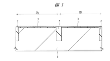
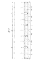
本実施の形態の半導体装置の製造工程を図面を参照して説明する。図1〜図15は、本発明の一実施の形態である半導体装置、ここではCMISFET(Complementary Metal Insulator Semiconductor Field Effect Transistor)を有する半導体装置の製造工程中の要部断面図である。
(Embodiment 1)
A manufacturing process of the semiconductor device of the present embodiment will be described with reference to the drawings. FIG. 1 to FIG. 15 are cross-sectional views of a principal part during a manufacturing process of a semiconductor device according to an embodiment of the present invention, here, a semiconductor device having a CMISFET (Complementary Metal Insulator Semiconductor Field Effect Transistor).

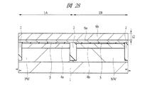
まず、図1に示されるように、例えば1〜10Ωcm程度の比抵抗を有するp型の単結晶シリコンなどからなる半導体基板(半導体ウエハ)1を準備する。それから、半導体基板1の主面に素子分離領域2を形成する。素子分離領域2は酸化シリコンなどの絶縁体からなり、例えばSTI(Shallow Trench Isolation)法またはLOCOS(Local Oxidization of Silicon)法などにより形成される。例えば、半導体基板1に形成された溝(素子分離溝)に埋め込まれた絶縁膜により、素子分離領域2を形成することができる。素子分離領域2によって、nチャネル型MISFET(Metal Insulator Semiconductor Field Effect Transistor:MIS型電界効果トランジスタ)Qnが形成される領域(活性領域)であるnMIS形成領域1Aと、pチャネル型MISFETQpが形成される領域(活性領域)であるpMIS形成領域1Bとが規定される。   First, as shown in FIG. 1, a semiconductor substrate (semiconductor wafer) 1 made of, for example, p-type single crystal silicon having a specific resistance of about 1 to 10 Ωcm is prepared. Then, the element isolation region 2 is formed on the main surface of the semiconductor substrate 1. The element isolation region 2 is made of an insulator such as silicon oxide, and is formed by, for example, an STI (Shallow Trench Isolation) method or a LOCOS (Local Oxidization of Silicon) method. For example, the element isolation region 2 can be formed by an insulating film embedded in a groove (element isolation groove) formed in the semiconductor substrate 1. The element isolation region 2 forms an nMIS formation region 1A, which is a region (active region) where an n-channel MISFET (Metal Insulator Semiconductor Field Effect Transistor) Qn is formed, and a p-channel MISFET Qp. A pMIS formation region 1B which is a region (active region) is defined.

次に、表面の汚染防止のための薄い絶縁膜(スルー膜)3を半導体基板1の表面(主面)に形成してから、図2に示されるように、pMIS形成領域1Bを覆うフォトレジスト膜(フォトレジストパターン)RP1aを、フォトリソグラフィ技術を用いて形成する。nMIS形成領域1Aは、このフォトレジスト膜RP1aでは覆われずに露出される。このフォトレジスト膜RP1aは、pMIS形成領域1Bへのイオン注入阻止マスクとして機能することができる。   Next, after forming a thin insulating film (through film) 3 for preventing surface contamination on the surface (main surface) of the semiconductor substrate 1, as shown in FIG. 2, a photoresist covering the pMIS formation region 1B. A film (photoresist pattern) RP1a is formed using a photolithography technique. The nMIS formation region 1A is exposed without being covered with the photoresist film RP1a. The photoresist film RP1a can function as an ion implantation blocking mask for the pMIS formation region 1B.

次に、nMIS形成領域1Aにおいて、半導体基板1の上層部分に、後で形成されるnチャネル型MISFETQnのしきい値調整用のイオン注入(すなわちチャネルドープイオン注入)IM1aを行なう。なお、図2では、チャネルドープイオン注入IM1aを矢印で模式的に示してある。   Next, in the nMIS formation region 1A, ion implantation for adjusting a threshold value of an n channel MISFET Qn (that is, channel dope ion implantation) IM1a is performed on the upper layer portion of the semiconductor substrate 1 later. In FIG. 2, the channel dope ion implantation IM1a is schematically indicated by an arrow.

MIFETのしきい値調整用のイオン注入は、チャネルドープイオン注入と呼ぶこともでき、このチャネルドープイオン注入(しきい値調整用のイオン注入)によって、MISFETのチャネル領域に不純物が導入(ドープ)される。すなわち、チャネルドープイオン注入では、MISFETのチャネル領域を含む領域に、不純物(不純物イオン)が導入(ドープ)される。なお、ここでいう「MISFETのチャネル領域」とは、チャネルドープイオン注入の段階ではMISFETは形成されていなくとも、その後MISFETが形成されると、MISFETのチャネル領域となる領域に対応する。このことは、本実施の形態1および以下の実施の形態2〜6で述べるチャネルドープイオン注入(しきい値調整用のイオン注入)に共通である。   The ion implantation for adjusting the threshold value of the MISFET can also be referred to as channel doping ion implantation. By this channel doping ion implantation (ion implantation for adjusting the threshold value), impurities are introduced (doped) into the channel region of the MISFET. Is done. That is, in channel dope ion implantation, impurities (impurity ions) are introduced (doped) into a region including the channel region of the MISFET. The “channel region of the MISFET” here corresponds to a region that becomes a channel region of the MISFET when the MISFET is formed afterwards even though the MISFET is not formed at the channel doping ion implantation stage. This is common to channel dope ion implantation (threshold adjustment ion implantation) described in the first embodiment and the following second to sixth embodiments.

しきい値調整用のイオン注入IM1a、すなわちチャネルドープイオン注入IM1aでは、nチャネル型MISFETQnのチャネル領域を含む領域に、不純物(不純物イオン)が導入(イオン注入)されて、チャネルドープ層4aが形成される。このチャネルドープ層4aは、後でnチャネル型MISFETQnのチャネル領域となる領域を含んでいる。チャネルドープイオン注入IM1aによってチャネルドープ層4aに導入される不純物は、例えばホウ素(B)などのp型の不純物を用いることができる。このチャネルドープイオン注入IM1aでは、pMIS形成領域1Bを覆うフォトレジスト膜RP1aは、イオン注入阻止マスクとして機能するので、pMIS形成領域1Bの半導体基板1には、イオン注入されない。   In the ion implantation IM1a for adjusting the threshold, that is, the channel dope ion implantation IM1a, impurities (impurity ions) are introduced (ion implantation) into a region including the channel region of the n-channel MISFET Qn to form the channel dope layer 4a. Is done. The channel dope layer 4a includes a region that later becomes a channel region of the n-channel type MISFET Qn. As an impurity introduced into the channel dope layer 4a by the channel dope ion implantation IM1a, for example, a p-type impurity such as boron (B) can be used. In this channel dope ion implantation IM1a, the photoresist film RP1a covering the pMIS formation region 1B functions as an ion implantation blocking mask, so that ions are not implanted into the semiconductor substrate 1 in the pMIS formation region 1B.

次に、nMIS形成領域1Aにおいて、半導体基板1の主面から所定の深さに渡ってp型ウエル(p型半導体領域)PWを形成する。p型ウエルPWは、pMIS形成領域1Bを覆うフォトレジスト膜RP1aをイオン注入阻止マスクとして、nMIS形成領域1Aの半導体基板1に例えばホウ素(B)などのp型の不純物をイオン注入することなどによって形成することができる。なお、チャネルドープ層4aは、半導体基板1の上層部分に浅く形成され、p型ウエルPWは、半導体基板1において、チャネルドープ層4aよりも深くまで形成されている。また、他の形態として、先にp型ウエルPWをイオン注入で形成してから、チャネルドープイオン注入IM1aによってチャネルドープ層4aを形成することもでき、これは以下の実施の形態2〜4でも同様である。   Next, in the nMIS formation region 1A, a p-type well (p-type semiconductor region) PW is formed from the main surface of the semiconductor substrate 1 to a predetermined depth. The p-type well PW is formed by, for example, ion-implanting a p-type impurity such as boron (B) into the semiconductor substrate 1 in the nMIS formation region 1A using the photoresist film RP1a covering the pMIS formation region 1B as an ion implantation blocking mask. Can be formed. The channel dope layer 4a is formed shallow in the upper layer portion of the semiconductor substrate 1, and the p-type well PW is formed deeper than the channel dope layer 4a in the semiconductor substrate 1. As another form, the p-type well PW can be formed by ion implantation first, and then the channel dope ion implantation IM1a can be used to form the channel dope layer 4a. This is also the case with the following second to fourth embodiments. It is the same.

次に、図3に示されるように、アッシングなどによりフォトレジスト膜RP1aを除去してから、nMIS形成領域1Aを覆うフォトレジスト膜(フォトレジストパターン)RP1bを、フォトリソグラフィ技術を用いて形成する。pMIS形成領域1Bは、このフォトレジスト膜RP1bでは覆われずに露出される。このフォトレジスト膜RP1bは、nMIS形成領域1Aへのイオン注入阻止マスクとして機能することができる。   Next, as shown in FIG. 3, after removing the photoresist film RP1a by ashing or the like, a photoresist film (photoresist pattern) RP1b covering the nMIS formation region 1A is formed by using a photolithography technique. The pMIS formation region 1B is exposed without being covered with the photoresist film RP1b. The photoresist film RP1b can function as an ion implantation blocking mask for the nMIS formation region 1A.

次に、pMIS形成領域1Bにおいて、半導体基板1の上層部分に、後で形成されるpチャネル型MISFETQpのしきい値調整用のイオン注入(すなわちチャネルドープイオン注入)IM1bを行なう。なお、図3では、チャネルドープイオン注入IM1bを矢印で模式的に示してある。   Next, in the pMIS formation region 1B, ion implantation for adjusting a threshold value of a p-channel type MISFET Qp to be formed later (that is, channel dope ion implantation) IM1b is performed on the upper layer portion of the semiconductor substrate 1. In FIG. 3, the channel dope ion implantation IM1b is schematically indicated by an arrow.

しきい値調整用のイオン注入IM1b、すなわちチャネルドープイオン注入IM1bでは、pチャネル型MISFETQpのチャネル領域を含む領域に、不純物(不純物イオン)が導入(イオン注入)されて、チャネルドープ層4bが形成される。このチャネルドープ層4bは、後でpチャネル型MISFETQpのチャネル領域となる領域を含んでいる。チャネルドープイオン注入によってチャネルドープ層4bに導入される不純物は、例えばリン(P)などのn型の不純物を用いることができる。このチャネルドープイオン注入IM1bでは、nMIS形成領域1Aを覆うフォトレジスト膜RP1bは、イオン注入阻止マスクとして機能するので、nMIS形成領域1Aの半導体基板1には、イオン注入されない。   In the ion implantation IM1b for adjusting the threshold, that is, the channel dope ion implantation IM1b, impurities (impurity ions) are introduced (ion implantation) into a region including the channel region of the p-channel MISFET Qp to form the channel dope layer 4b. Is done. This channel dope layer 4b includes a region that will later become a channel region of the p-channel type MISFET Qp. As an impurity introduced into the channel dope layer 4b by channel dope ion implantation, for example, an n-type impurity such as phosphorus (P) can be used. In this channel dope ion implantation IM1b, the photoresist film RP1b covering the nMIS formation region 1A functions as an ion implantation blocking mask, so that ions are not implanted into the semiconductor substrate 1 in the nMIS formation region 1A.

次に、pMIS形成領域1Bにおいて、半導体基板1の主面から所定の深さに渡ってn型ウエル(n型半導体領域)NWを形成する。n型ウエルNWは、nMIS形成領域1Aを覆うフォトレジスト膜RP1bをイオン注入阻止マスクとして、pMIS形成領域1Bの半導体基板1に例えばリン(P)などのn型の不純物をイオン注入することなどによって形成することができる。なお、チャネルドープ層4bは、半導体基板1の上層部分に浅く形成され、n型ウエルNWは、半導体基板1において、チャネルドープ層4bよりも深くまで形成されている。また、他の形態として、先にn型ウエルNWをイオン注入で形成してから、チャネルドープイオン注入IM1bによってチャネルドープ層4bを形成することもでき、これは以下の実施の形態2〜4でも同様である。更に他の形態として、先にpMIS形成領域1Bにチャネルドープ層4bおよびn型ウエルNWを形成した後で、nMIS形成領域1Aにチャネルドープ層4aおよびp型ウエルPWを形成することもでき、これは以下の実施の形態2〜4でも同様である。   Next, in the pMIS formation region 1B, an n-type well (n-type semiconductor region) NW is formed from the main surface of the semiconductor substrate 1 to a predetermined depth. The n-type well NW is formed by, for example, ion-implanting n-type impurities such as phosphorus (P) into the semiconductor substrate 1 in the pMIS formation region 1B using the photoresist film RP1b covering the nMIS formation region 1A as an ion implantation blocking mask. Can be formed. The channel dope layer 4b is formed shallow in the upper layer portion of the semiconductor substrate 1, and the n-type well NW is formed deeper than the channel dope layer 4b in the semiconductor substrate 1. As another form, the n-type well NW can be formed by ion implantation first, and then the channel dope ion implantation IM1b can be used to form the channel dope layer 4b. This is also the case in the following second to fourth embodiments. It is the same. As yet another form, after the channel dope layer 4b and the n-type well NW are first formed in the pMIS formation region 1B, the channel dope layer 4a and the p-type well PW can be formed in the nMIS formation region 1A. The same applies to the following second to fourth embodiments.

次に、図4に示されるように、アッシングなどによりフォトレジスト膜RP1bを除去してから、例えばフッ酸(HF)水溶液を用いたウェットエッチングなどにより上記絶縁膜3を除去して半導体基板1の表面を清浄化(洗浄)した後、nMIS形成領域1AおよびpMIS形成領域1Bの半導体基板1の表面(主面、ここではp型ウエルPWおよびn型ウエルNWの表面)上にゲート絶縁膜用の絶縁膜(第1絶縁膜)5を形成する。この絶縁膜5は、後でnチャネル型MISFETQnおよびpチャネル型MISFETQpのゲート絶縁膜となる。絶縁膜5は、例えば薄い酸化シリコン膜などからなり、例えば熱酸化法などによって形成することができる。   Next, as shown in FIG. 4, after removing the photoresist film RP <b> 1 b by ashing or the like, the insulating film 3 is removed by wet etching using a hydrofluoric acid (HF) aqueous solution, for example. After the surface is cleaned (washed), the gate insulating film is formed on the surface of the semiconductor substrate 1 (main surface, here, the surface of the p-type well PW and the n-type well NW) in the nMIS formation region 1A and the pMIS formation region 1B. An insulating film (first insulating film) 5 is formed. This insulating film 5 will later become a gate insulating film of the n-channel MISFET Qn and the p-channel MISFET Qp. The insulating film 5 is made of, for example, a thin silicon oxide film, and can be formed by, for example, a thermal oxidation method.

次に、半導体基板1の主面全面上(すなわちnMIS形成領域1AおよびpMIS形成領域1Bの絶縁膜5上を含む)に、ゲート電極形成用の導電体膜として、多結晶シリコン膜のようなシリコン膜6を形成する。シリコン膜6のうちのnMIS形成領域1A(後述するゲート電極GE1となる領域)は、フォトレジスト膜(図示せず)をマスクとして用いてリン(P)またはヒ素(As)などのn型の不純物をイオン注入することなどにより、低抵抗のn型半導体膜(ドープトポリシリコン膜)とされている。また、シリコン膜6のうちのpMIS形成領域1B(後述するゲート電極GE2となる領域)は、他のフォトレジスト膜(図示せず)をマスクとして用いてホウ素(B)などのp型の不純物をイオン注入することなどにより、低抵抗のp型半導体膜(ドープトポリシリコン膜)とされている。また、シリコン膜6は、成膜時にはアモルファスシリコン膜であったものを、成膜後(イオン注入後)の熱処理により多結晶シリコン膜に変えることもできる。   Next, on the entire main surface of the semiconductor substrate 1 (that is, on the insulating film 5 in the nMIS formation region 1A and the pMIS formation region 1B), a silicon film such as a polycrystalline silicon film is formed as a conductor film for forming a gate electrode. A film 6 is formed. The nMIS formation region 1A (region to be a gate electrode GE1 described later) in the silicon film 6 is an n-type impurity such as phosphorus (P) or arsenic (As) using a photoresist film (not shown) as a mask. Is ion-implanted to form a low-resistance n-type semiconductor film (doped polysilicon film). Further, the pMIS formation region 1B (region to be a gate electrode GE2 described later) in the silicon film 6 is made of p-type impurities such as boron (B) using another photoresist film (not shown) as a mask. By ion implantation or the like, a low-resistance p-type semiconductor film (doped polysilicon film) is obtained. Further, the silicon film 6 can be changed from an amorphous silicon film at the time of film formation to a polycrystalline silicon film by heat treatment after film formation (after ion implantation).

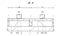
次に、図5に示されるように、シリコン膜6をフォトリソグラフィ法およびドライエッチング法を用いてパターニングすることにより、ゲート電極GE1,GE2を形成する。   Next, as shown in FIG. 5, the silicon film 6 is patterned using a photolithography method and a dry etching method, thereby forming gate electrodes GE1 and GE2.

nチャネル型MISFETQnのゲート電極となるゲート電極GE1は、n型の不純物を導入した多結晶シリコン(n型半導体膜、ドープトポリシリコン膜)からなり、nMIS形成領域1Aのp型ウエルPW(の上部のチャネルドープ層4a)上に絶縁膜5を介して形成される。ゲート電極GE1の下に残存する絶縁膜5が、nチャネル型MISFETQnのゲート絶縁膜5aとなる。すなわち、ゲート電極GE1は、nMIS形成領域1Aの絶縁膜5(すなわちゲート絶縁膜5a)上に形成される。また、pチャネル型MISFETQpのゲート電極となるゲート電極GE2は、p型の不純物を導入した多結晶シリコン(p型半導体膜、ドープトポリシリコン膜)からなり、pMIS形成領域1Bのn型ウエルNW(の上部のチャネルドープ層4b)上に絶縁膜5を介して形成される。ゲート電極GE2の下に残存する絶縁膜5が、pチャネル型MISFETQpのゲート絶縁膜5bとなる。すなわち、ゲート電極GE2は、pMIS形成領域1Bの絶縁膜5(すなわちゲート絶縁膜5b)上に形成される。   The gate electrode GE1 serving as the gate electrode of the n-channel type MISFET Qn is made of polycrystalline silicon (n-type semiconductor film, doped polysilicon film) into which an n-type impurity is introduced, and the p-type well PW (of the nMIS formation region 1A) An insulating film 5 is formed on the upper channel doped layer 4a). The insulating film 5 remaining under the gate electrode GE1 becomes the gate insulating film 5a of the n-channel type MISFET Qn. That is, the gate electrode GE1 is formed on the insulating film 5 (that is, the gate insulating film 5a) in the nMIS formation region 1A. Further, the gate electrode GE2 serving as the gate electrode of the p-channel type MISFET Qp is made of polycrystalline silicon (p-type semiconductor film, doped polysilicon film) into which p-type impurities are introduced, and the n-type well NW in the pMIS formation region 1B. (On the upper channel doped layer 4b) with an insulating film 5 interposed therebetween. The insulating film 5 remaining under the gate electrode GE2 becomes the gate insulating film 5b of the p-channel type MISFET Qp. That is, the gate electrode GE2 is formed on the insulating film 5 (that is, the gate insulating film 5b) in the pMIS formation region 1B.

次に、図6に示されるように、pMIS形成領域1Bを覆うフォトレジスト膜(フォトレジストパターン)RP2aを、フォトリソグラフィ技術を用いて形成する。nMIS形成領域1Aは、このフォトレジスト膜RP2aでは覆われずに露出される。このフォトレジスト膜RP2aは、pMIS形成領域1Bへのイオン注入阻止マスクとして機能することができる。このため、後述するイオン注入IM2a,IM3a,IM4aでは、フォトレジスト膜RP2aがイオン注入阻止マスクとして機能し、pMIS形成領域1Bの半導体基板1にはイオン注入されない。   Next, as shown in FIG. 6, a photoresist film (photoresist pattern) RP2a covering the pMIS formation region 1B is formed using a photolithography technique. The nMIS formation region 1A is exposed without being covered with the photoresist film RP2a. The photoresist film RP2a can function as an ion implantation blocking mask for the pMIS formation region 1B. For this reason, in ion implantation IM2a, IM3a, and IM4a described later, the photoresist film RP2a functions as an ion implantation blocking mask, and ions are not implanted into the semiconductor substrate 1 in the pMIS formation region 1B.

次に、nMIS形成領域1Aの半導体基板1(p型ウエルPW)のゲート電極GE1の両側の領域に、リン(P)またはヒ素(As)などのn型の不純物をイオン注入することにより、(一対の)エクステンション領域(第1半導体領域、ソース・ドレインエクステンション領域、n型半導体領域)7aを形成する。エクステンション領域7aはn型の半導体領域であり、後で形成するn型半導体領域11aよりも不純物濃度が低い。なお、図6では、エクステンション領域7aを形成するためのイオン注入IM2aを矢印で模式的に示してある。このイオン注入IM2aの際、ゲート電極GE1もマスク(イオン注入阻止マスク)として機能することができるので、エクステンション領域7aは、ゲート電極GE1(の側壁)に整合して形成され、ゲート電極GE1の直下には、不純物は導入(イオン注入)されない。エクステンション領域7aの深さ(接合深さ)は、後で形成されるn型半導体領域11aの深さ(接合深さ)よりも浅い。また、エクステンション領域7a形成のためのイオン注入IM2aは、斜めイオン注入ではなく、半導体基板1の主面に対して垂直な方向にイオン注入することが好ましい。 Next, n-type impurities such as phosphorus (P) or arsenic (As) are ion-implanted into regions on both sides of the gate electrode GE1 of the semiconductor substrate 1 (p-type well PW) in the nMIS formation region 1A. A pair of extension regions (first semiconductor region, source / drain extension region, n type semiconductor region) 7 a is formed. The extension region 7a is an n-type semiconductor region, and has an impurity concentration lower than that of the n + -type semiconductor region 11a to be formed later. In FIG. 6, ion implantation IM2a for forming the extension region 7a is schematically indicated by an arrow. In this ion implantation IM2a, since the gate electrode GE1 can also function as a mask (ion implantation blocking mask), the extension region 7a is formed in alignment with the gate electrode GE1 (side wall thereof) and directly below the gate electrode GE1. No impurities are introduced (ion implantation). The depth (junction depth) of the extension region 7a is shallower than the depth (junction depth) of the n + type semiconductor region 11a to be formed later. Further, the ion implantation IM2a for forming the extension region 7a is preferably not the oblique ion implantation but the ion implantation in the direction perpendicular to the main surface of the semiconductor substrate 1.

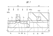
次に、図7に示されるように、nMIS形成領域1Aの半導体基板1(p型ウエルPW)にp型不純物のイオン注入(ハローイオン注入)IM3aを行ってハロー領域(p型半導体領域)8aを形成する。なお、図7では、ハロー領域8aを形成するためのイオン注入(ハローイオン注入)IM3aを矢印で模式的に示してある。ハロー領域8aは、エクステンション領域7aとは逆の導電型で、かつp型ウエルPWとは同じ導電型であり、ここではp型(p型の半導体領域)である。ハロー領域8aは、短チャネル特性抑制のために形成される。ハロー領域8aを形成するためのイオン注入IM3aの際、ゲート電極GE1もマスク(イオン注入阻止マスク)として機能することができる。ハロー領域8aは、エクステンション領域7aを包み込む(覆う)ように形成され、p型ウエルPWよりも不純物濃度(p型不純物濃度)が高い。ハロー領域8aを形成するためのイオン注入IM3aは、斜めイオン注入(傾斜イオン注入)とすることがより好ましく、これにより、エクステンション領域7aを包み込む(覆う)ようにハロー領域8aを的確に形成することができる。なお、一般のイオン注入では、半導体基板1の主面に対して垂直な方向に不純物イオンを加速して打ち込むが、斜めイオン注入では、半導体基板1の主面に対して垂直な方向から所定の角度(傾斜角)傾斜した方向に不純物イオンを加速して打ち込む。   Next, as shown in FIG. 7, p-type impurity ion implantation (halo ion implantation) IM3a is performed on the semiconductor substrate 1 (p-type well PW) in the nMIS formation region 1A to form a halo region (p-type semiconductor region) 8a. Form. In FIG. 7, ion implantation (halo ion implantation) IM3a for forming the halo region 8a is schematically indicated by an arrow. The halo region 8a has a conductivity type opposite to that of the extension region 7a and the same conductivity type as that of the p-type well PW, and is a p-type (p-type semiconductor region) here. The halo region 8a is formed to suppress short channel characteristics. In the ion implantation IM3a for forming the halo region 8a, the gate electrode GE1 can also function as a mask (ion implantation blocking mask). The halo region 8a is formed so as to enclose (cover) the extension region 7a, and has an impurity concentration (p-type impurity concentration) higher than that of the p-type well PW. The ion implantation IM3a for forming the halo region 8a is more preferably an oblique ion implantation (gradient ion implantation), whereby the halo region 8a is accurately formed so as to wrap (cover) the extension region 7a. Can do. In general ion implantation, impurity ions are accelerated and implanted in a direction perpendicular to the main surface of the semiconductor substrate 1. In oblique ion implantation, a predetermined direction from a direction perpendicular to the main surface of the semiconductor substrate 1 is used. Impurity ions are accelerated and implanted in an inclined direction.

次に、図8に示されるように、nMIS形成領域1Aの半導体基板1(p型ウエルPW)に第1元素のイオン注入IM4aを行って拡散防止領域10aを形成する。なお、図8では、拡散防止領域10aを形成するためのイオン注入IM4aを矢印で模式的に示してある。このイオン注入IM4aの際、ゲート電極GE1もマスク(イオン注入阻止マスク)として機能することができる。拡散防止領域10aは、第1元素が導入(ドープ)された領域である。拡散防止領域10aを形成するためのイオン注入IM4aで半導体基板1に注入される第1元素は、炭素(C)、窒素(N)またはフッ素(F)のうちの1種以上からなる。拡散防止領域10aにおける第1元素の濃度は、イオン注入IM4aの注入量(ドーズ量)で例えば5×10¹⁴〜5×10¹⁵/cm程度、体積濃度で例えば1×1018〜1×1020/cm程度とすることができる。 Next, as shown in FIG. 8, the diffusion prevention region 10a is formed by ion implantation IM4a of the first element in the semiconductor substrate 1 (p-type well PW) in the nMIS formation region 1A. In FIG. 8, the ion implantation IM4a for forming the diffusion prevention region 10a is schematically indicated by an arrow. In this ion implantation IM4a, the gate electrode GE1 can also function as a mask (ion implantation blocking mask). The diffusion preventing region 10a is a region where the first element is introduced (doped). The first element implanted into the semiconductor substrate 1 by the ion implantation IM4a for forming the diffusion prevention region 10a is made of one or more of carbon (C), nitrogen (N), and fluorine (F). The concentration of the first element in the diffusion preventing region 10a is, for example, about 5 × 10 14 to 5 × 10 15 / cm 2 in terms of the implantation amount (dose amount) of the ion implantation IM4a, and in the volume concentration, for example, 1 × 10 18 to 1 × 10. It can be about 20 / cm 3 .

拡散防止領域10aは、エクステンション領域7a、ハロー領域8a、および後述のn型半導体領域11aを形成する際のイオン注入で生成された点欠陥が、nチャネル型MISFETQnのチャネル領域に拡散するのを防止する機能を有している。このため、拡散防止領域10aは、その少なくとも一部が、エクステンション領域7a、ハロー領域8a、および後述のn型半導体領域11aと、nチャネル型MISFETQnのチャネル領域との間に位置する必要がある。従って、ハロー領域8aを包み込む(覆う)ように拡散防止領域10aを形成することが好ましい。 The diffusion prevention region 10a prevents point defects generated by ion implantation when forming the extension region 7a, the halo region 8a, and an n + type semiconductor region 11a described later from diffusing into the channel region of the n channel MISFET Qn. It has a function to prevent. For this reason, at least a part of the diffusion prevention region 10a needs to be located between the extension region 7a, the halo region 8a, the n + type semiconductor region 11a described later, and the channel region of the n channel MISFET Qn. . Therefore, it is preferable to form the diffusion preventing region 10a so as to wrap (cover) the halo region 8a.

このため、拡散防止領域10a形成のためのイオン注入IM4aでは、ハロー領域8aよりも深い位置に上記第1元素をイオン注入することが好ましい。また、拡散防止領域10a形成のためのイオン注入IM4aは、斜めイオン注入(傾斜イオン注入)とすることが好ましい。これにより、ハロー領域8aとnチャネル型MISFETQnのチャネル領域との間に拡散防止領域10aを的確に位置させることができるようになる。   For this reason, in the ion implantation IM4a for forming the diffusion prevention region 10a, it is preferable to ion-implant the first element at a position deeper than the halo region 8a. Further, the ion implantation IM4a for forming the diffusion prevention region 10a is preferably oblique ion implantation (tilted ion implantation). As a result, the diffusion prevention region 10a can be accurately positioned between the halo region 8a and the channel region of the n-channel type MISFET Qn.

また、拡散防止領域10aを形成するためのイオン注入IM4aの傾斜角を、ハロー領域8aを形成するためのイオン注入IM3aの傾斜角よりも大きくすれば、更に好ましい。これにより、ハロー領域8aとnチャネル型MISFETQnのチャネル領域との間に拡散防止領域10aを更に的確に位置させることができるようになる。ここで、イオン注入の傾斜角とは、イオン注入方向の半導体基板1の主面に垂直な方向からの傾斜角に対応し、半導体基板1の主面に垂直な方向に不純物イオンを打ち込む場合は、傾斜角は0°である。   Further, it is more preferable that the inclination angle of the ion implantation IM4a for forming the diffusion prevention region 10a is larger than the inclination angle of the ion implantation IM3a for forming the halo region 8a. As a result, the diffusion prevention region 10a can be positioned more accurately between the halo region 8a and the channel region of the n-channel type MISFET Qn. Here, the tilt angle of ion implantation corresponds to the tilt angle from the direction perpendicular to the main surface of the semiconductor substrate 1 in the ion implantation direction, and when impurity ions are implanted in the direction perpendicular to the main surface of the semiconductor substrate 1. The tilt angle is 0 °.

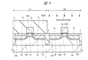
次に、図9に示されるように、アッシングなどによりフォトレジスト膜RP2aを除去してから、nMIS形成領域1Aを覆うフォトレジスト膜(フォトレジストパターン)RP2bを、フォトリソグラフィ技術を用いて形成する。pMIS形成領域1Bは、このフォトレジスト膜RP2bでは覆われずに露出される。このフォトレジスト膜RP2bは、nMIS形成領域1Aへのイオン注入阻止マスクとして機能することができる。このため、後述するイオン注入IM2b,IM3b,IM4bでは、フォトレジスト膜RP2bがイオン注入阻止マスクとして機能し、nMIS形成領域1Aの半導体基板1にはイオン注入されない。   Next, as shown in FIG. 9, after removing the photoresist film RP2a by ashing or the like, a photoresist film (photoresist pattern) RP2b covering the nMIS formation region 1A is formed by using a photolithography technique. The pMIS formation region 1B is exposed without being covered with the photoresist film RP2b. The photoresist film RP2b can function as an ion implantation blocking mask for the nMIS formation region 1A. For this reason, in ion implantation IM2b, IM3b, and IM4b described later, the photoresist film RP2b functions as an ion implantation blocking mask, and ions are not implanted into the semiconductor substrate 1 in the nMIS formation region 1A.

次に、pMIS形成領域1Bの半導体基板1(n型ウエルNW)のゲート電極GE2の両側の領域に、ホウ素(B)などのp型の不純物をイオン注入することにより、(一対の)エクステンション領域(第1半導体領域、ソース・ドレインエクステンション領域、p型半導体領域)7bを形成する。エクステンション領域7bはp型の半導体領域であり、後で形成するp型半導体領域11bよりも不純物濃度が低い。なお、エクステンション領域7bを形成するためのイオン注入IM2bと、後述するハロー領域8bを形成するためのイオン注入IM3bと、後述する拡散防止領域10bを形成するためのイオン注入IM4bとは、それぞれ別々のイオン注入工程として行なわれるが、図9では、まとめて矢印で模式的に示してある。 Next, a p-type impurity such as boron (B) is ion-implanted into regions on both sides of the gate electrode GE2 of the semiconductor substrate 1 (n-type well NW) in the pMIS formation region 1B, thereby (a pair of) extension regions. (First semiconductor region, source / drain extension region, p type semiconductor region) 7b is formed. The extension region 7b is a p-type semiconductor region, and has an impurity concentration lower than that of the p + -type semiconductor region 11b to be formed later. An ion implantation IM2b for forming the extension region 7b, an ion implantation IM3b for forming a halo region 8b described later, and an ion implantation IM4b for forming a diffusion prevention region 10b described later are respectively separate. Although it is performed as an ion implantation process, in FIG. 9, it is schematically shown by an arrow together.

エクステンション領域7bを形成するためのイオン注入IM2bでは、ゲート電極GE2もマスク(イオン注入阻止マスク)として機能することができるので、エクステンション領域7bは、ゲート電極GE2(の側壁)に整合して形成され、ゲート電極GE2の直下には、不純物は導入(イオン注入)されない。エクステンション領域7bの深さ(接合深さ)は、後で形成されるp型半導体領域11bの深さ(接合深さ)よりも浅い。また、エクステンション領域7b形成のためのイオン注入IM2bは、斜めイオン注入ではなく、半導体基板1の主面に対して垂直な方向にイオン注入することが好ましい。 In the ion implantation IM2b for forming the extension region 7b, the gate electrode GE2 can also function as a mask (ion implantation blocking mask). Therefore, the extension region 7b is formed in alignment with the gate electrode GE2 (side wall thereof). Impurities are not introduced (ion implantation) immediately below the gate electrode GE2. The depth (junction depth) of the extension region 7b is shallower than the depth (junction depth) of the p + type semiconductor region 11b to be formed later. Further, the ion implantation IM2b for forming the extension region 7b is preferably not ion implantation but oblique implantation in a direction perpendicular to the main surface of the semiconductor substrate 1.

次に、pMIS形成領域1Bの半導体基板1(n型ウエルNW)にn型不純物のイオン注入(ハローイオン注入)IM3bを行ってハロー領域(n型半導体領域)8bを形成する。ハロー領域8bは、エクステンション領域7bとは逆の導電型で、かつn型ウエルNWとは同じ導電型であり、ここではn型(n型の半導体領域)である。ハロー領域8bは、短チャネル特性抑制のために形成される。ハロー領域8bを形成するためのイオン注入IM3bの際、ゲート電極GE2もマスク(イオン注入阻止マスク)として機能することができる。ハロー領域8bは、エクステンション領域7bを包み込む(覆う)ように形成され、n型ウエルNWよりも不純物濃度(n型不純物濃度)が高い。ハロー領域8bを形成するためのイオン注入IM3bは、斜めイオン注入(傾斜イオン注入)とすることがより好ましく、これにより、エクステンション領域7bを包み込む(覆う)ようにハロー領域8bを的確に形成することができる。   Next, n-type impurity ion implantation (halo ion implantation) IM3b is performed on the semiconductor substrate 1 (n-type well NW) in the pMIS formation region 1B to form a halo region (n-type semiconductor region) 8b. The halo region 8b has a conductivity type opposite to that of the extension region 7b and the same conductivity type as that of the n-type well NW, and here is an n-type (n-type semiconductor region). The halo region 8b is formed for suppressing short channel characteristics. In the ion implantation IM3b for forming the halo region 8b, the gate electrode GE2 can also function as a mask (ion implantation blocking mask). The halo region 8b is formed so as to enclose (cover) the extension region 7b, and has an impurity concentration (n-type impurity concentration) higher than that of the n-type well NW. The ion implantation IM3b for forming the halo region 8b is more preferably an oblique ion implantation (gradient ion implantation), whereby the halo region 8b is accurately formed so as to wrap (cover) the extension region 7b. Can do.

次に、pMIS形成領域1Bの半導体基板1(n型ウエルNW)に第1元素のイオン注入IM4bを行って拡散防止領域10bを形成する。拡散防止領域10bは、第1元素が導入(ドープ)された領域である。このイオン注入IM4bの際、ゲート電極GE2もマスク(イオン注入阻止マスク)として機能することができる。拡散防止領域10bを形成するためのイオン注入IM4bで注入される第1元素は、炭素(C)、窒素(N)またはフッ素(F)のうちの1種以上からなる。拡散防止領域10bにおける第1元素の濃度は、イオン注入IM4bの注入量(ドーズ量)で例えば5×10¹⁴〜5×10¹⁵/cm程度、体積濃度で例えば1×1018〜1×1020/cm程度とすることができる。 Next, a first element ion implantation IM4b is performed on the semiconductor substrate 1 (n-type well NW) in the pMIS formation region 1B to form a diffusion prevention region 10b. The diffusion prevention region 10b is a region into which the first element is introduced (doped). During the ion implantation IM4b, the gate electrode GE2 can also function as a mask (ion implantation blocking mask). The first element implanted by the ion implantation IM4b for forming the diffusion prevention region 10b is made of one or more of carbon (C), nitrogen (N), and fluorine (F). The concentration of the first element in the diffusion prevention region 10b is, for example, about 5 × 10 14 to 5 × 10 15 / cm 2 in terms of the implantation amount (dose amount) of the ion implantation IM4b, and in the volume concentration, for example, 1 × 10 18 to 1 × 10. It can be about 20 / cm 3 .

拡散防止領域10bは、エクステンション領域7b、ハロー領域8b、および後述のp型半導体領域11bを形成する際のイオン注入で生成された点欠陥が、pチャネル型MISFETQpのチャネル領域に拡散するのを防止する機能を有している。このため、拡散防止領域10bは、その少なくとも一部が、エクステンション領域7b、ハロー領域8b、および後述のp型半導体領域11bと、pチャネル型MISFETQpのチャネル領域との間に位置する必要がある。従って、ハロー領域8bを包み込む(覆う)ように拡散防止領域10bを形成することが好ましい。 The diffusion prevention region 10b prevents the point defects generated by ion implantation when forming the extension region 7b, the halo region 8b, and the p + type semiconductor region 11b described later from diffusing into the channel region of the p channel MISFET Qp. It has a function to prevent. For this reason, at least a part of the diffusion prevention region 10b needs to be located between the extension region 7b, the halo region 8b, the p + type semiconductor region 11b described later, and the channel region of the p channel type MISFET Qp. . Therefore, it is preferable to form the diffusion prevention region 10b so as to wrap (cover) the halo region 8b.

このため、拡散防止領域10b形成のためのイオン注入IM4bでは、ハロー領域8bよりも深い位置に上記第1元素をイオン注入することが好ましい。また、拡散防止領域10b形成のためのイオン注入IM4bは、斜めイオン注入(傾斜イオン注入)とすることが好ましい。これにより、ハロー領域8bとnチャネル型MISFETQpのチャネル領域との間に拡散防止領域10bを的確に位置させることができるようになる。   For this reason, in the ion implantation IM4b for forming the diffusion prevention region 10b, it is preferable to ion-implant the first element at a position deeper than the halo region 8b. The ion implantation IM4b for forming the diffusion prevention region 10b is preferably an oblique ion implantation (gradient ion implantation). Thereby, the diffusion prevention region 10b can be accurately positioned between the halo region 8b and the channel region of the n-channel type MISFET Qp.

また、拡散防止領域10bを形成するためのイオン注入IM4bの傾斜角を、ハロー領域8bを形成するためのイオン注入の傾斜角よりも大きくすれば、更に好ましい。これにより、ハロー領域8bとpチャネル型MISFETQpのチャネル領域との間に拡散防止領域10bを更に的確に位置させることができるようになる。   It is further preferable that the inclination angle of the ion implantation IM4b for forming the diffusion prevention region 10b is larger than the inclination angle of the ion implantation for forming the halo region 8b. As a result, the diffusion prevention region 10b can be positioned more accurately between the halo region 8b and the channel region of the p-channel type MISFET Qp.

また、他の形態として、先にpMIS形成領域1Bにエクステンション領域7b、ハロー領域8bおよび拡散防止領域10bを形成してから、nMIS形成領域1Aにエクステンション領域7a、ハロー領域8aおよび拡散防止領域10aを形成することもでき、これは以下の実施の形態2〜4でも同様である。   As another form, after the extension region 7b, the halo region 8b, and the diffusion prevention region 10b are first formed in the pMIS formation region 1B, the extension region 7a, the halo region 8a, and the diffusion prevention region 10a are formed in the nMIS formation region 1A. It can also be formed, and this is the same in the following second to fourth embodiments.

また、ハロー領域8a,8bは、短チャネル特性抑制のために形成することが好ましいが、不要であればその形成を省略することもでき、これは以下の実施の形態2〜4でも同様である。   The halo regions 8a and 8b are preferably formed to suppress short channel characteristics. However, the formation of the halo regions 8a and 8b can be omitted if unnecessary, and this is the same in the following second to fourth embodiments. .

また、エクステンション領域7a、ハロー領域8aおよび拡散防止領域10aは、必ずしもこの順序で形成しなくともよいが、エクステンション領域7a、ハロー領域8aおよび拡散防止領域10aを形成する各イオン注入IM2a,IM3a,IM4aは、少なくとも、ゲート電極GE1形成後で、かつ、ゲート電極GE1の側壁上に後述のサイドウォールSWを形成する前に行う必要がある。同様に、エクステンション領域7b、ハロー領域8bおよび拡散防止領域10bは、必ずしもこの順序で形成しなくともよいが、エクステンション領域7b、ハロー領域8bおよび拡散防止領域10bを形成する各イオン注入IM2b,IM3b,IM4bは、少なくとも、ゲート電極GE2形成後で、かつ、ゲート電極GE2の側壁上に後述のサイドウォールSWを形成する前に行う必要がある。   Further, the extension region 7a, the halo region 8a, and the diffusion prevention region 10a are not necessarily formed in this order, but the respective ion implantations IM2a, IM3a, IM4a for forming the extension region 7a, the halo region 8a, and the diffusion prevention region 10a. It is necessary to perform at least after forming the gate electrode GE1 and before forming a sidewall SW described later on the sidewall of the gate electrode GE1. Similarly, the extension region 7b, the halo region 8b, and the diffusion prevention region 10b do not necessarily have to be formed in this order, but the respective ion implantations IM2b, IM3b, which form the extension region 7b, the halo region 8b, and the diffusion prevention region 10b, IM4b needs to be performed at least after forming the gate electrode GE2 and before forming a later-described sidewall SW on the sidewall of the gate electrode GE2.

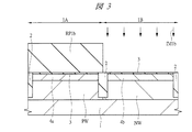
次に、図10に示されるように、アッシングなどによりフォトレジスト膜RP2bを除去してから、ゲート電極GE1,GE2の側壁上に、絶縁膜(側壁絶縁膜)として、例えば酸化シリコンまたは窒化シリコンあるいはそれら絶縁膜の積層膜などからなる側壁スペーサまたはサイドウォール(側壁絶縁膜、サイドウォールスペーサ)SWを形成する。サイドウォールSWは、例えば、半導体基板1(の主面全面)上に酸化シリコン膜または窒化シリコン膜あるいはそれらの積層膜を堆積し、この酸化シリコン膜または窒化シリコン膜あるいはそれらの積層膜をRIE(Reactive Ion Etching:反応性イオンエッチング)法などにより異方性エッチングすることによって形成することができる。   Next, as shown in FIG. 10, after removing the photoresist film RP2b by ashing or the like, as an insulating film (sidewall insulating film) on the side walls of the gate electrodes GE1 and GE2, for example, silicon oxide or silicon nitride or Sidewall spacers or sidewalls (sidewall insulating films, sidewall spacers) SW made of a laminated film of these insulating films are formed. For example, the sidewall SW is formed by depositing a silicon oxide film, a silicon nitride film, or a laminated film thereof on the semiconductor substrate 1 (entire main surface thereof), and depositing the silicon oxide film, the silicon nitride film, or the laminated film thereof by RIE ( Reactive Ion Etching (reactive ion etching) can be formed by anisotropic etching.

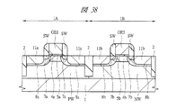
次に、図11に示されるように、pMIS形成領域1Bを覆うフォトレジスト膜(フォトレジストパターン)RP3aを、フォトリソグラフィ技術を用いて形成する。nMIS形成領域1Aは、このフォトレジスト膜RP3aでは覆われずに露出される。このフォトレジスト膜RP3aは、pMIS形成領域1Bへのイオン注入阻止マスクとして機能することができる。このため、後述するイオン注入IM5aでは、フォトレジスト膜RP3aがイオン注入阻止マスクとして機能し、pMIS形成領域1Bの半導体基板1にはイオン注入されない。   Next, as shown in FIG. 11, a photoresist film (photoresist pattern) RP3a covering the pMIS formation region 1B is formed using a photolithography technique. The nMIS formation region 1A is exposed without being covered with the photoresist film RP3a. The photoresist film RP3a can function as an ion implantation blocking mask for the pMIS formation region 1B. For this reason, in the ion implantation IM5a described later, the photoresist film RP3a functions as an ion implantation blocking mask, and ions are not implanted into the semiconductor substrate 1 in the pMIS formation region 1B.

次に、nMIS形成領域1Aの半導体基板1(p型ウエルPW)のゲート電極GE1およびサイドウォールSWの両側の領域に、リン(P)またはヒ素(As)などのn型の不純物をイオン注入することにより、(一対の)n型半導体領域11a(ソース、ドレイン)を形成する。なお、図11では、n型半導体領域11aを形成するためのイオン注入IM5aを矢印で模式的に示してある。このイオン注入IM5aの際、ゲート電極GE1およびその側壁上のサイドウォールSWもマスク(イオン注入阻止マスク)として機能することができるので、n型半導体領域11aは、ゲート電極GE1の側壁上のサイドウォールSW(の側壁)に整合して形成され、ゲート電極GE1およびサイドウォールSWの直下には、不純物は導入(イオン注入)されない。n型半導体領域11aの深さ(接合深さ)は、エクステンション領域7aの深さ(接合深さ)よりも深い。 Next, an n-type impurity such as phosphorus (P) or arsenic (As) is ion-implanted into regions on both sides of the gate electrode GE1 and the sidewall SW of the semiconductor substrate 1 (p-type well PW) in the nMIS formation region 1A. Thereby, (a pair of) n + type semiconductor regions 11a (source and drain) are formed. In FIG. 11, ion implantation IM5a for forming the n + type semiconductor region 11a is schematically indicated by an arrow. In this ion implantation IM5a, since the gate electrode GE1 and the sidewall SW on the side wall thereof can also function as a mask (ion implantation blocking mask), the n + -type semiconductor region 11a is formed on the side wall on the side wall of the gate electrode GE1. Impurities are not introduced (ion-implanted) immediately below the gate electrode GE1 and the side wall SW. The depth (junction depth) of the n + -type semiconductor region 11a is deeper than the depth (junction depth) of the extension region 7a.

型半導体領域(第2半導体領域)11aとエクステンション領域(第1半導体領域)7aとは同じ導電型であるが、n型半導体領域11aは、エクステンション領域7aよりも、不純物濃度(n型不純物濃度)が高い。これにより、nチャネル型MISFETQnのソースまたはドレインとして機能するn型の半導体領域(不純物拡散層)が、n型半導体領域(不純物拡散層)11aおよびエクステンション領域(n型半導体領域)7aにより形成される。換言すれば、エクステンション領域7aと、それよりも高不純物濃度のn型半導体領域11aとは、nチャネル型MISFETQnのソースまたはドレイン用の半導体領域として機能する。従って、nチャネル型MISFETQnのソース・ドレイン領域は、LDD(Lightly doped Drain)構造を有している。上述のように、エクステンション領域7aは、ゲート電極GE1に対して自己整合的に形成され、n型半導体領域11aは、ゲート電極GE1の側壁上に形成されたサイドウォールSWに対して自己整合的に形成される。 The n + type semiconductor region (second semiconductor region) 11a and the extension region (first semiconductor region) 7a have the same conductivity type, but the n + type semiconductor region 11a has an impurity concentration (n type) than the extension region 7a. Impurity concentration) is high. Thereby, an n-type semiconductor region (impurity diffusion layer) functioning as a source or drain of the n-channel type MISFET Qn is formed by the n + -type semiconductor region (impurity diffusion layer) 11a and the extension region (n -type semiconductor region) 7a. Is done. In other words, the extension region 7a and the n + type semiconductor region 11a having a higher impurity concentration function as a semiconductor region for the source or drain of the n-channel type MISFET Qn. Therefore, the source / drain region of the n-channel type MISFET Qn has an LDD (Lightly doped Drain) structure. As described above, the extension region 7a is formed in a self-aligned manner with respect to the gate electrode GE1, and the n + type semiconductor region 11a is in a self-aligned manner with respect to the sidewall SW formed on the sidewall of the gate electrode GE1. Formed.

また、サイドウォールSWの形成後、n型半導体領域11a形成用のイオン注入の前または後に、半導体基板1に炭素(C)、窒素(N)またはフッ素(F)のうちの1種以上からなる第1元素をイオン注入することもできる。この場合、このイオン注入で第1元素が注入された領域が、n型半導体領域11aを包み込む(覆う)ようにすることが好ましい。これにより、n型半導体領域11aに生成された点欠陥が、nチャネル型MISFETQnのチャネル領域に拡散するのを、更に的確に防止することができる。 In addition, after forming the sidewall SW, before or after ion implantation for forming the n + -type semiconductor region 11a, the semiconductor substrate 1 is made of one or more of carbon (C), nitrogen (N), and fluorine (F). The first element can be ion-implanted. In this case, it is preferable that the region implanted with the first element by this ion implantation wraps (covers) the n + type semiconductor region 11a. Thereby, it is possible to more accurately prevent the point defect generated in the n + type semiconductor region 11a from diffusing into the channel region of the n channel type MISFET Qn.

次に、図12に示されるように、アッシングなどによりフォトレジスト膜RP3aを除去してから、nMIS形成領域1Aを覆うフォトレジスト膜(フォトレジストパターン)RP3bを、フォトリソグラフィ技術を用いて形成する。pMIS形成領域1Bは、このフォトレジスト膜RP3bでは覆われずに露出される。このフォトレジスト膜RP3bは、nMIS形成領域1Aへのイオン注入阻止マスクとして機能することができる。このため、後述するイオン注入IM5bでは、フォトレジスト膜RP3bがイオン注入阻止マスクとして機能し、nMIS形成領域1Aの半導体基板1にはイオン注入されない。   Next, as shown in FIG. 12, after removing the photoresist film RP3a by ashing or the like, a photoresist film (photoresist pattern) RP3b covering the nMIS formation region 1A is formed by using a photolithography technique. The pMIS formation region 1B is exposed without being covered with the photoresist film RP3b. The photoresist film RP3b can function as an ion implantation blocking mask for the nMIS formation region 1A. For this reason, in ion implantation IM5b described later, the photoresist film RP3b functions as an ion implantation blocking mask, and ions are not implanted into the semiconductor substrate 1 in the nMIS formation region 1A.

次に、pMIS形成領域1Bの半導体基板1(n型ウエルNW)のゲート電極GE2およびサイドウォールSWの両側の領域に、ホウ素(B)などのp型の不純物をイオン注入することにより、(一対の)p型半導体領域11b(ソース、ドレイン)を形成する。なお、図12では、p型半導体領域11bを形成するためのイオン注入IM5bを矢印で模式的に示してある。このイオン注入IM5bの際、ゲート電極GE2およびその側壁上のサイドウォールSWもマスク(イオン注入阻止マスク)として機能することができるので、p型半導体領域11bは、ゲート電極GE2の側壁上のサイドウォールSW(の側壁)に整合して形成され、ゲート電極GE2およびサイドウォールSWの直下には、不純物は導入(イオン注入)されない。p型半導体領域11bの深さ(接合深さ)は、エクステンション領域7bの深さ(接合深さ)よりも深い。 Next, a p-type impurity such as boron (B) is ion-implanted into regions on both sides of the gate electrode GE2 and the side wall SW of the semiconductor substrate 1 (n-type well NW) in the pMIS formation region 1B. The p + type semiconductor region 11b (source, drain) is formed. In FIG. 12, ion implantation IM5b for forming the p + type semiconductor region 11b is schematically indicated by an arrow. In this ion implantation IM5b, the gate electrode GE2 and the sidewall SW on the side wall thereof can also function as a mask (ion implantation blocking mask), so that the p + type semiconductor region 11b is formed on the side of the gate electrode GE2 on the side wall. Impurities are not introduced (ion-implanted) immediately below the gate electrode GE2 and the side wall SW. The depth (junction depth) of the p + -type semiconductor region 11b is deeper than the depth (junction depth) of the extension region 7b.

型半導体領域(第2半導体領域)11bとエクステンション領域(第1半導体領域)7bとは同じ導電型であるが、p型半導体領域11bは、エクステンション領域7bよりも、不純物濃度(p型不純物濃度)が高い。これにより、pチャネル型MISFETQpのソースまたはドレインとして機能するp型の半導体領域(不純物拡散層)が、p型半導体領域(不純物拡散層)11bおよびエクステンション領域(p型半導体領域)7bにより形成される。換言すれば、エクステンション領域7bと、それよりも高不純物濃度のp型半導体領域11bとは、pチャネル型MISFETQpのソースまたはドレイン用の半導体領域として機能する。従って、pチャネル型MISFETQpのソース・ドレイン領域は、LDD構造を有している。上述のように、エクステンション領域7bは、ゲート電極GE2に対して自己整合的に形成され、p型半導体領域11bは、ゲート電極GE2の側壁上に形成されたサイドウォールSWに対して自己整合的に形成される。 The p + type semiconductor region (second semiconductor region) 11b and the extension region (first semiconductor region) 7b have the same conductivity type, but the impurity concentration (p type) of the p + type semiconductor region 11b is higher than that of the extension region 7b. Impurity concentration) is high. Thereby, a p-type semiconductor region (impurity diffusion layer) functioning as a source or drain of the p-channel type MISFET Qp is formed by the p + -type semiconductor region (impurity diffusion layer) 11b and the extension region (p -type semiconductor region) 7b. Is done. In other words, the extension region 7b and the p + type semiconductor region 11b having a higher impurity concentration function as a semiconductor region for the source or drain of the p-channel type MISFET Qp. Therefore, the source / drain regions of the p-channel type MISFET Qp have an LDD structure. As described above, the extension region 7b is formed in a self-aligned manner with respect to the gate electrode GE2, and the p + type semiconductor region 11b is in a self-aligned manner with respect to the sidewall SW formed on the side wall of the gate electrode GE2. Formed.

また、サイドウォールSWの形成後、p型半導体領域11b形成用のイオン注入の前または後に、半導体基板1に炭素(C)、窒素(N)またはフッ素(F)のうちの1種以上からなる第1元素をイオン注入することもできる。この場合、このイオン注入で第1元素が注入された領域が、p型半導体領域11bを包み込む(覆う)ようにすることが好ましい。これにより、p型半導体領域11bに生成された点欠陥が、pチャネル型MISFETQpのチャネル領域に拡散するのを、更に的確に防止することができる。 In addition, after forming the sidewall SW, before or after ion implantation for forming the p + -type semiconductor region 11b, the semiconductor substrate 1 is made of one or more of carbon (C), nitrogen (N), and fluorine (F). The first element can be ion-implanted. In this case, it is preferable that the region implanted with the first element by this ion implantation wraps (covers) the p + type semiconductor region 11b. Thereby, it is possible to more accurately prevent the point defects generated in the p + type semiconductor region 11b from diffusing into the channel region of the p channel type MISFET Qp.

また、他の形態として、先にpMIS形成領域1Bにp型半導体領域11bを形成してから、nMIS形成領域1Aにn型半導体領域11aを形成することもでき、これは以下の実施の形態2〜4でも同様である。 As another form, after forming the p + type semiconductor region 11b in the pMIS formation region 1B first, the n + type semiconductor region 11a can be formed in the nMIS formation region 1A. The same applies to Embodiments 2 to 4.

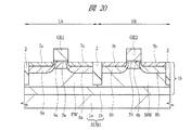
次に、アッシングなどによりフォトレジスト膜RP3bを除去する。それから、これまでのイオン注入で導入した不純物の活性化のためのアニール処理(熱処理)を行う。このアニール処理は、例えば1050℃程度のスパイクアニール処理にて行うことができる。   Next, the photoresist film RP3b is removed by ashing or the like. Then, annealing treatment (heat treatment) for activating the impurities introduced by the conventional ion implantation is performed. This annealing process can be performed, for example, by a spike annealing process at about 1050 ° C.

このようにして、nMIS形成領域1A(のp型ウエルPW)に、電界効果トランジスタとしてnチャネル型MISFET(Metal Insulator Semiconductor Field Effect Transistor)Qnが形成される。また、pMIS形成領域1B(のn型ウエルNW)に、電界効果トランジスタとしてpチャネル型MISFET(Metal Insulator Semiconductor Field Effect Transistor)Qpが形成される。これにより、図13の構造が得られる。nチャネル型MISFETQnは、nチャネル型の電界効果トランジスタとみなすことができ、pチャネル型MISFETQpは、pチャネル型の電界効果トランジスタとみなすことができる。   In this manner, an n-channel MISFET (Metal Insulator Semiconductor Field Effect Transistor) Qn is formed as a field effect transistor in the nMIS formation region 1A (the p-type well PW). A p-channel MISFET (Metal Insulator Semiconductor Field Effect Transistor) Qp is formed as a field effect transistor in the pMIS formation region 1B (n-type well NW thereof). Thereby, the structure of FIG. 13 is obtained. The n-channel type MISFET Qn can be regarded as an n-channel field effect transistor, and the p-channel type MISFET Qp can be regarded as a p-channel field effect transistor.

次に、ゲート電極GE1,GE2、n型半導体領域11aおよびp型半導体領域11bの表面を露出させ、例えばコバルト(Co)膜またはニッケル(Ni)のような金属膜を堆積して熱処理することによって、図14に示されるように、ゲート電極GE1,GE2、n型半導体領域11aおよびp型半導体領域11bの表面に、それぞれ金属シリサイド層12を形成する。これにより、n型半導体領域11aおよびp型半導体領域11bの拡散抵抗やコンタクト抵抗などを低抵抗化することができる。その後、未反応の金属膜は除去する。 Next, the surfaces of the gate electrodes GE1, GE2, the n + type semiconductor region 11a and the p + type semiconductor region 11b are exposed, and a metal film such as a cobalt (Co) film or nickel (Ni) is deposited and heat-treated. As a result, as shown in FIG. 14, metal silicide layers 12 are formed on the surfaces of the gate electrodes GE1, GE2, the n + type semiconductor region 11a and the p + type semiconductor region 11b, respectively. Thereby, the diffusion resistance, contact resistance, etc. of the n + type semiconductor region 11a and the p + type semiconductor region 11b can be reduced. Thereafter, the unreacted metal film is removed.

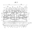
次に、半導体基板1の主面上に絶縁膜21を形成する。すなわち、ゲート電極GE1,GE2を覆うように、金属シリサイド層12上を含む半導体基板1上に絶縁膜21を形成する。絶縁膜21は例えば窒化シリコン膜からなり、プラズマCVD法などを用いて形成することができる。それから、絶縁膜21上に絶縁膜21よりも厚い絶縁膜22を形成する。絶縁膜22は例えば酸化シリコン膜などからなり、TEOS(Tetraethoxysilane:テトラエトキシシラン、またはTetra Ethyl Ortho Silicateとも言う)を用いてプラズマCVD法などにより形成することができる。これにより、絶縁膜21,22からなる層間絶縁膜が形成される。その後、絶縁膜22の表面をCMP法により研磨するなどして、絶縁膜22の上面を平坦化する。下地段差に起因して絶縁膜21の表面に凹凸形状が形成されていても、絶縁膜22の表面をCMP法により研磨することにより、その表面が平坦化された層間絶縁膜を得ることができる。   Next, an insulating film 21 is formed on the main surface of the semiconductor substrate 1. That is, the insulating film 21 is formed on the semiconductor substrate 1 including the metal silicide layer 12 so as to cover the gate electrodes GE1 and GE2. The insulating film 21 is made of, for example, a silicon nitride film, and can be formed using a plasma CVD method or the like. Then, an insulating film 22 thicker than the insulating film 21 is formed on the insulating film 21. The insulating film 22 is made of, for example, a silicon oxide film or the like, and can be formed by a plasma CVD method or the like using TEOS (Tetraethoxysilane: Tetra Ethyl Ortho Silicate). Thereby, an interlayer insulating film composed of the insulating films 21 and 22 is formed. Thereafter, the upper surface of the insulating film 22 is planarized by polishing the surface of the insulating film 22 by CMP or the like. Even if unevenness is formed on the surface of the insulating film 21 due to the base step, by polishing the surface of the insulating film 22 by the CMP method, an interlayer insulating film having a flattened surface can be obtained. .

次に、絶縁膜22上に形成したフォトレジストパターン(図示せず)をエッチングマスクとして用いて、絶縁膜22,21をドライエッチングすることにより、絶縁膜22,21にコンタクトホール(貫通孔、孔)23を形成する。この際、まず絶縁膜21に比較して絶縁膜22がエッチングされやすい条件で絶縁膜22のドライエッチングを行い、絶縁膜21をエッチングストッパ膜として機能させることで、絶縁膜22にコンタクトホール23を形成してから、絶縁膜22に比較して絶縁膜21がエッチングされやすい条件でコンタクトホール23の底部の絶縁膜21をドライエッチングして除去する。コンタクトホール23の底部では、半導体基板1の主面の一部、例えばn型半導体領域11aおよびp型半導体領域11bの表面上の金属シリサイド層12の一部や、ゲート電極GE1,GE2の表面上の金属シリサイド層12の一部などが露出される。 Next, by using the photoresist pattern (not shown) formed on the insulating film 22 as an etching mask, the insulating films 22 and 21 are dry-etched to form contact holes (through holes, holes) in the insulating films 22 and 21. ) 23. At this time, first, the insulating film 22 is dry-etched under conditions that allow the insulating film 22 to be etched more easily than the insulating film 21, and the insulating film 21 functions as an etching stopper film, whereby the contact hole 23 is formed in the insulating film 22. After the formation, the insulating film 21 at the bottom of the contact hole 23 is removed by dry etching under the condition that the insulating film 21 is more easily etched than the insulating film 22. At the bottom of the contact hole 23, a part of the main surface of the semiconductor substrate 1, for example, a part of the metal silicide layer 12 on the surface of the n + type semiconductor region 11a and the p + type semiconductor region 11b, and the gate electrodes GE1 and GE2 A part of the metal silicide layer 12 on the surface is exposed.

次に、コンタクトホール23内に、タングステン(W)などからなるプラグ(接続用導体部)24を形成する。プラグ24を形成するには、例えば、コンタクトホール23の内部(底部および側壁上)を含む絶縁膜22上に、プラズマCVD法によりバリア導体膜24a(例えばチタン膜、窒化チタン膜、あるいはそれらの積層膜)を形成する。それから、タングステン膜などからなる主導体膜24bをCVD法などによってバリア導体膜24a上にコンタクトホール23を埋めるように形成し、絶縁膜22上の不要な主導体膜24bおよびバリア導体膜24aをCMP法またはエッチバック法などによって除去することにより、プラグ24を形成することができる。ゲート電極GE1,GE2、n型半導体領域11aまたはp型半導体領域11b上に形成されたプラグ24は、その底部でゲート電極GE1,GE2、n型半導体領域11aまたはp型半導体領域11bの表面上の金属シリサイド層12と接して、電気的に接続される。 Next, a plug (connecting conductor portion) 24 made of tungsten (W) or the like is formed in the contact hole 23. In order to form the plug 24, for example, a barrier conductor film 24a (for example, a titanium film, a titanium nitride film, or a laminate thereof) is formed on the insulating film 22 including the inside (on the bottom and side walls) of the contact hole 23 by a plasma CVD method. Film). Then, a main conductor film 24b made of a tungsten film or the like is formed so as to fill the contact hole 23 on the barrier conductor film 24a by CVD or the like, and the unnecessary main conductor film 24b and barrier conductor film 24a on the insulating film 22 are CMPed. The plug 24 can be formed by removing it by the method or the etch back method. The plug 24 formed on the gate electrodes GE1, GE2, n + type semiconductor region 11a or p + type semiconductor region 11b has a gate electrode GE1, GE2, n + type semiconductor region 11a or p + type semiconductor region 11b at the bottom. The metal silicide layer 12 on the surface of the metal is in contact with and electrically connected.

次に、図15に示されるように、プラグ24が埋め込まれた絶縁膜22上に、ストッパ絶縁膜25および配線形成用の絶縁膜26を順次形成する。ストッパ絶縁膜25は絶縁膜26への溝加工の際にエッチングストッパとなる膜であり、絶縁膜26に対してエッチング選択比を有する材料を用いる。ストッパ絶縁膜25は、例えばプラズマCVD法により形成される窒化シリコン膜とし、絶縁膜26は、例えばプラズマCVD法により形成される酸化シリコン膜とすることができる。なお、ストッパ絶縁膜25と絶縁膜26には、次に説明する第1層目の配線が形成される。   Next, as shown in FIG. 15, a stopper insulating film 25 and a wiring forming insulating film 26 are sequentially formed on the insulating film 22 in which the plugs 24 are embedded. The stopper insulating film 25 is a film that becomes an etching stopper when the groove is formed in the insulating film 26, and a material having an etching selectivity with respect to the insulating film 26 is used. The stopper insulating film 25 can be a silicon nitride film formed by, for example, plasma CVD, and the insulating film 26 can be, for example, a silicon oxide film formed by plasma CVD. The stopper insulating film 25 and the insulating film 26 are formed with a first layer wiring described below.

次に、シングルダマシン法により第1層目の配線を形成する。まず、フォトレジストパターン(図示せず)をマスクとしたドライエッチングによって絶縁膜26およびストッパ絶縁膜25の所定の領域に配線溝27を形成した後、半導体基板1の主面上(すなわち配線溝27の底部および側壁上を含む絶縁膜26上)にバリア導体膜(バリアメタル膜)28を形成する。バリア導体膜28は、例えば窒化チタン膜、タンタル膜または窒化タンタル膜などを用いることができる。続いて、CVD法またはスパッタリング法などによりバリア導体膜28上に銅のシード層を形成し、さらに電解めっき法などを用いてシード層上に銅めっき膜を形成して、銅めっき膜により配線溝27の内部を埋め込む。図15では、シード膜および銅めっき膜を合わせたものを銅の主導体膜29として図示している。それから、配線溝27以外の領域の主導体膜29(銅めっき膜およびシード層)とバリアメタル膜28をCMP法により除去して、配線溝27に埋め込まれ銅を主導電材料とする第1層目の配線M1を形成する。配線M1は、プラグ24を介してnチャネル型MISFETQnおよびpチャネル型MISFETQpのソースまたはドレイン用のn型半導体領域11aおよびp型半導体領域11bやゲート電極GE1,GE2などと電気的に接続されている。その後、デュアルダマシン法により2層目の配線を形成するが、ここでは図示およびその説明は省略する。 Next, a first layer wiring is formed by a single damascene method. First, after forming a wiring groove 27 in a predetermined region of the insulating film 26 and the stopper insulating film 25 by dry etching using a photoresist pattern (not shown) as a mask, the wiring groove 27 is formed on the main surface of the semiconductor substrate 1 (that is, the wiring groove 27). A barrier conductor film (barrier metal film) 28 is formed on the insulating film 26 including the bottom and side walls. As the barrier conductor film 28, for example, a titanium nitride film, a tantalum film, a tantalum nitride film, or the like can be used. Subsequently, a copper seed layer is formed on the barrier conductor film 28 by a CVD method or a sputtering method, and further a copper plating film is formed on the seed layer by an electrolytic plating method or the like. 27 is embedded. In FIG. 15, a combination of the seed film and the copper plating film is shown as a copper main conductor film 29. Then, the main conductor film 29 (copper plating film and seed layer) and the barrier metal film 28 in the region other than the wiring groove 27 are removed by CMP, and the first layer is buried in the wiring groove 27 and uses copper as the main conductive material. An eye wiring M1 is formed. The wiring M1 is electrically connected to the n + -type semiconductor region 11a and p + -type semiconductor region 11b for the source or drain of the n-channel type MISFET Qn and p-channel type MISFET Qp, the gate electrodes GE1, GE2, etc. via the plug 24. ing. Thereafter, a second layer wiring is formed by a dual damascene method, but illustration and description thereof are omitted here.

次に、本実施の形態の効果について、より詳細に説明する。   Next, the effect of this embodiment will be described in more detail.

半導体基板に不純物をイオン注入した場合、注入直後の段階では、注入された不純物はランダムに配置されているが、その後の種々の加熱工程で不純物が拡散(移動)すると、不純物のランダム配置が崩れ、注入直後に比べて不純物の分布に偏りが生じてしまう。すなわち、イオン注入した直後の段階では、注入した不純物の配置のランダム性が高いが、その後の種々の加熱工程で不純物が拡散(移動)すると、不純物の配置のランダム性が低下してしまう。このことは、イオン注入が、MISFETのしきい値調整用のチャネルドープイオン注入である場合でも同様である。従って、チャネルドープイオン注入した直後の段階では、チャネル領域にドープされた不純物の配置のランダム性が高いが、その後の種々の加熱工程で不純物が拡散(移動)すると、チャネル領域にドープされた不純物の配置のランダム性が低下してしまう。   When an impurity is ion-implanted into a semiconductor substrate, the implanted impurity is randomly arranged at the stage immediately after the implantation. However, when the impurity diffuses (moves) in various subsequent heating processes, the random arrangement of the impurity is destroyed. As a result, the distribution of impurities is biased compared to immediately after the implantation. That is, in the stage immediately after ion implantation, the randomness of the arrangement of implanted impurities is high, but if the impurities diffuse (move) in various subsequent heating steps, the randomness of the arrangement of impurities deteriorates. This is the same even when the ion implantation is channel doping ion implantation for adjusting the threshold value of the MISFET. Accordingly, in the stage immediately after channel doping ion implantation, the arrangement of impurities doped in the channel region is highly random, but when the impurities diffuse (move) in various subsequent heating processes, the impurities doped in the channel region The randomness of the arrangement of will be reduced.

なお、不純物の配置のランダム性が高い状態では、微視的(原子配列のレベル)には、不純物は均一(規則的)に配置されているのではなく、ばらばら(ランダム)に存在しているが、微視的にランダムであるが故に、巨視的(チャネル領域のレベル)には、不純物は偏りなく同じように分布している。このため、不純物の配置のランダム性が高い状態では、チャネル領域同士を比べたときの不純物分布の違い(あるMISFETのチャネル領域の不純物分布と他のMISFETのチャネル領域の不純物分布との差)が小さく、MISFETのしきい値のばらつきが小さい。   In addition, in a state where the randomness of the arrangement of impurities is high, the impurities are not arranged uniformly (regularly) microscopically (at the level of atomic arrangement) but are present in a random (random) manner. However, since they are microscopically random, the impurities are distributed equally in a macroscopic manner (channel region level). For this reason, in a state where the randomness of the impurity arrangement is high, the difference in impurity distribution (difference between the impurity distribution in the channel region of one MISFET and the impurity distribution in the channel region of another MISFET) when the channel regions are compared with each other. Small, variation in threshold of MISFET is small.

しかしながら、不純物配置のランダム性が低下すると、この状態が崩れ、巨視的な不純物の分布(チャネル領域のレベルでの不純物分布)に偏りが生じてしまう。このため、チャネルドープイオン注入後に、熱拡散によってチャネルドープ不純物の配置のランダム性が低くなった状態では、チャネル領域同士を比べたときの不純物分布の違い(あるMISFETのチャネル領域の不純物分布と他のMISFETのチャネル領域の不純物分布との差)が大きくなり、MISFETのしきい値のばらつきが大きくなってしまう。すなわち、MISFET毎にチャネル領域の状態(チャネル領域における不純物の配置状態)が変動してしまい、MISFET毎にしきい値電圧が変動してしまうのである。半導体装置の性能を向上させるためには、MISFET毎のしきい値電圧のばらつきを抑制することが望まれる。   However, if the randomness of the impurity arrangement decreases, this state collapses, and the macroscopic impurity distribution (impurity distribution at the channel region level) is biased. For this reason, after the channel doping ion implantation, in the state where the randomness of the channel doping impurities is reduced by thermal diffusion, the difference in the impurity distribution when comparing the channel regions (impurity distribution in the channel region of a certain MISFET and others) (Difference from the impurity distribution in the channel region of the MISFET) increases, and the variation in threshold value of the MISFET increases. That is, the state of the channel region (arrangement state of impurities in the channel region) varies for each MISFET, and the threshold voltage varies for each MISFET. In order to improve the performance of the semiconductor device, it is desired to suppress variations in threshold voltage for each MISFET.

このため、チャネルドープイオン注入で導入された不純物が、その後の加熱工程の際に再配置(拡散)されるのをできるだけ抑制して、注入直後のチャネルドープ不純物の配置(ランダム性が高い配置)を注入後もできるだけ維持することが、MISFET毎のしきい値電圧のばらつきを抑制するために重要である。   For this reason, it is possible to suppress as much as possible the impurities introduced in the channel doping ion implantation from being rearranged (diffused) during the subsequent heating process, and to arrange the channel doped impurities immediately after the implantation (arrangement with high randomness). It is important to maintain as much as possible after the implantation in order to suppress variation in threshold voltage for each MISFET.

また、半導体基板1にイオン注入を行なうと、半導体基板1の不純物イオンがドープされた領域に点欠陥も生成されてしまうが、点欠陥は拡散しやすい。このため、エクステンション領域7a,7b、ハロー領域8a,8b、n型半導体領域11aおよびp型半導体領域11bを形成する際の各イオン注入で生成された点欠陥が、その後の種々の加熱工程でMISFETのチャネル領域(ゲート電極GE1,GE2の直下の領域)にまで拡散してしまう可能性がある。特に、エクステンション領域7a,7bおよびハロー領域8a,8bは、チャネル領域(ゲート電極GE1,GE2の直下の領域)に近いため、イオン注入でエクステンション領域7a,7bおよびハロー領域8a,8bに生成された点欠陥が、チャネル領域にまで拡散しやすい。点欠陥がチャネル領域に拡散すると、チャネル領域における点欠陥の密度が大きくなるが、点欠陥の密度が大きいほど、チャネルドープイオン注入でチャネル領域に導入された不純物が移動(拡散)しやすくなる。これは、点欠陥が多いと、点欠陥を介して不純物が移動(拡散)しやすくなるためである。 Further, when ion implantation is performed on the semiconductor substrate 1, point defects are also generated in the region of the semiconductor substrate 1 doped with impurity ions, but the point defects are easily diffused. For this reason, the point defects generated by the respective ion implantations when forming the extension regions 7a and 7b, the halo regions 8a and 8b, the n + type semiconductor region 11a and the p + type semiconductor region 11b are caused by various subsequent heating processes. Thus, there is a possibility of diffusing up to the channel region of MISFET (region immediately below gate electrodes GE1 and GE2). In particular, since the extension regions 7a and 7b and the halo regions 8a and 8b are close to the channel region (the region immediately below the gate electrodes GE1 and GE2), they are generated in the extension regions 7a and 7b and the halo regions 8a and 8b by ion implantation. Point defects are likely to diffuse into the channel region. When point defects diffuse into the channel region, the density of point defects in the channel region increases. However, the larger the density of point defects, the easier the impurities introduced into the channel region by channel doping ion implantation move (diffuse). This is because when there are many point defects, impurities easily move (diffuse) through the point defects.

このため、チャネルドープイオン注入で導入した不純物が、その後の種々の加熱工程の際に再配置(拡散)されるのをできるだけ抑制するためには、エクステンション領域7a,7b、ハロー領域8a,8b、n型半導体領域11aおよびp型半導体領域11bを形成する際の各イオン注入で生成された点欠陥がチャネル領域にまで拡散してしまうのをできるだけ防止し、チャネル領域における点欠陥の密度を抑制することが有効である。 For this reason, in order to suppress as much as possible the impurities introduced by channel dope ion implantation from being rearranged (diffused) during various subsequent heating steps, the extension regions 7a and 7b, the halo regions 8a and 8b, Point defects generated by each ion implantation when forming the n + type semiconductor region 11a and the p + type semiconductor region 11b are prevented from diffusing into the channel region as much as possible, and the density of point defects in the channel region is reduced. It is effective to suppress.

本発明者の検討によれば、単結晶シリコンからなる基板領域(半導体基板1)に炭素(C)、窒素(N)またはフッ素(F)のうちの1種以上が導入された領域(本実施の形態の拡散防止領域10a,10bに対応)は、点欠陥が拡散(移動)しにくく、点欠陥の拡散(移動)を防止する機能を有していることが分かった。   According to the study of the present inventor, a region in which at least one of carbon (C), nitrogen (N), and fluorine (F) is introduced into a substrate region (semiconductor substrate 1) made of single crystal silicon (this embodiment) It was found that the diffusion preventing regions 10a and 10b in the form of (1) have a function of preventing the point defects from being diffused (moved) and preventing the point defects from being diffused (moved).

そこで、本実施の形態では、上述のように、nMIS形成領域1Aの半導体基板1(p型ウエルPW)に、炭素(C)、窒素(N)またはフッ素(F)のうちの1種以上(すなわち第1元素)をイオン注入して、拡散防止領域10aを形成している。また、上述のように、pMIS形成領域1Bの半導体基板1(n型ウエルNW)に、炭素(C)、窒素(N)またはフッ素(F)のうちの1種以上(すなわち第1元素)をイオン注入して、拡散防止領域10bを形成している。   Therefore, in the present embodiment, as described above, one or more of carbon (C), nitrogen (N), and fluorine (F) is applied to the semiconductor substrate 1 (p-type well PW) in the nMIS formation region 1A ( That is, the first element) is ion-implanted to form the diffusion prevention region 10a. Further, as described above, one or more of carbon (C), nitrogen (N), and fluorine (F) (that is, the first element) is applied to the semiconductor substrate 1 (n-type well NW) in the pMIS formation region 1B. Ion implantation is performed to form the diffusion prevention region 10b.

炭素(C)、窒素(N)またはフッ素(F)のうちの1種以上が導入された領域である拡散防止領域10aは、エクステンション領域7a、ハロー領域8a、およびn型半導体領域11aを形成する際の各イオン注入で生成された点欠陥が、nチャネル型MISFETQnのチャネル領域(ゲート電極GE1の直下の領域)にまで拡散するのを防止する機能を有している。また、炭素(C)、窒素(N)またはフッ素(F)のうちの1種以上が導入された領域である拡散防止領域10bは、エクステンション領域7b、ハロー領域8b、およびp型半導体領域11bを形成する際の各イオン注入で生成された点欠陥が、pチャネル型MISFETQpのチャネル領域(ゲート電極GE2の直下の領域)にまでに拡散するのを防止する機能を有している。 The diffusion prevention region 10a, which is a region into which one or more of carbon (C), nitrogen (N), or fluorine (F) is introduced, forms an extension region 7a, a halo region 8a, and an n + type semiconductor region 11a. It has a function of preventing the point defects generated by the respective ion implantations from being diffused to the channel region of the n-channel type MISFET Qn (the region immediately below the gate electrode GE1). The diffusion prevention region 10b, which is a region into which one or more of carbon (C), nitrogen (N), and fluorine (F) are introduced, includes an extension region 7b, a halo region 8b, and a p + type semiconductor region 11b. Has a function of preventing the point defects generated by the respective ion implantations during the formation of the diffusion into the channel region of the p-channel type MISFET Qp (region immediately below the gate electrode GE2).

上述の機能を拡散防止領域10aが有するためには、拡散防止領域10aの少なくとも一部が、エクステンション領域7a、ハロー領域8aおよびn型半導体領域11aと、nチャネル型MISFETQnのチャネル領域(ゲート電極GE1の直下の領域)との間に位置する必要がある。エクステンション領域7a、ハロー領域8aおよびn型半導体領域11aのうち、ハロー領域8aが最もnチャネル型MISFETQnのチャネル領域に近いため、ハロー領域8aを形成した場合は、拡散防止領域10aの少なくとも一部が、ハロー領域8aとnチャネル型MISFETQnのチャネル領域との間に位置すればよい。このようにするためには、ハロー領域8aを包み込む(覆う)ように拡散防止領域10aを形成することが好ましい。ハロー領域8aの形成を省略した場合は、エクステンション領域7aがチャネル領域に近いので、拡散防止領域10aの少なくとも一部が、エクステンション領域7aとnチャネル型MISFETQnのチャネル領域との間に位置すればよく、このようにするためには、エクステンション領域7aを包み込む(覆う)ように拡散防止領域10aを形成することが好ましい。 In order for the diffusion prevention region 10a to have the above-described function, at least a part of the diffusion prevention region 10a includes an extension region 7a, a halo region 8a, an n + type semiconductor region 11a, and a channel region (gate electrode) of the n channel MISFET Qn. It is necessary to be located between the region immediately below GE1). Of the extension region 7a, the halo region 8a, and the n + type semiconductor region 11a, the halo region 8a is closest to the channel region of the n-channel type MISFET Qn. Therefore, when the halo region 8a is formed, at least a part of the diffusion prevention region 10a May be positioned between the halo region 8a and the channel region of the n-channel MISFET Qn. In order to do this, it is preferable to form the diffusion preventing region 10a so as to wrap (cover) the halo region 8a. When the formation of the halo region 8a is omitted, since the extension region 7a is close to the channel region, at least a part of the diffusion prevention region 10a only needs to be located between the extension region 7a and the channel region of the n-channel type MISFET Qn. In order to do this, it is preferable to form the diffusion prevention region 10a so as to wrap (cover) the extension region 7a.

なお、拡散防止領域10aの少なくとも一部が、ハロー領域8aとnチャネル型MISFETQnのチャネル領域との間に位置する場合には、必然的に、エクステンション領域7aとnチャネル型MISFETQnのチャネル領域との間に拡散防止領域10aの少なくとも一部が位置することになる。このため、ハロー領域8aを形成するか否かにかかわらず、エクステンション領域7aとnチャネル型MISFETQnのチャネル領域との間に拡散防止領域10aの少なくとも一部を位置させ、ハロー領域8aを形成した場合には、ハロー領域8aとnチャネル型MISFETQnのチャネル領域との間に拡散防止領域10aの少なくとも一部が位置するようにすればよい。   When at least a part of the diffusion prevention region 10a is located between the halo region 8a and the channel region of the n-channel type MISFET Qn, the extension region 7a and the channel region of the n-channel type MISFET Qn are necessarily formed. At least a part of the diffusion prevention region 10a is located between them. Therefore, regardless of whether the halo region 8a is formed or not, the halo region 8a is formed by positioning at least a part of the diffusion prevention region 10a between the extension region 7a and the channel region of the n-channel type MISFET Qn. In other words, at least a part of the diffusion prevention region 10a may be positioned between the halo region 8a and the channel region of the n-channel type MISFET Qn.

また、上述の機能を拡散防止領域10bが有するためには、拡散防止領域10bの少なくとも一部が、エクステンション領域7b、ハロー領域8bおよびp型半導体領域11bと、pチャネル型MISFETQpのチャネル領域(ゲート電極GE2の直下の領域)との間に位置する必要がある。エクステンション領域7b、ハロー領域8bおよびp型半導体領域11bのうち、ハロー領域8bが最もpチャネル型MISFETQpのチャネル領域に近いため、ハロー領域8bを形成した場合は、拡散防止領域10bの少なくとも一部が、ハロー領域8bとpチャネル型MISFETQpのチャネル領域との間に位置すればよい。このようにするためには、ハロー領域8bを包み込む(覆う)ように拡散防止領域10bを形成することが好ましい。ハロー領域8bの形成を省略した場合は、エクステンション領域7bがチャネル領域に近いので、拡散防止領域10bの少なくとも一部が、エクステンション領域7bとpチャネル型MISFETQpのチャネル領域との間に位置すればよく、このようにするためには、エクステンション領域7bを包み込む(覆う)ように拡散防止領域10bを形成することが好ましい。 Further, in order for the diffusion prevention region 10b to have the above-described function, at least a part of the diffusion prevention region 10b includes the extension region 7b, the halo region 8b, the p + type semiconductor region 11b, and the channel region of the p channel MISFET Qp ( It is necessary to be located between the region immediately below the gate electrode GE2. Of the extension region 7b, the halo region 8b, and the p + type semiconductor region 11b, the halo region 8b is closest to the channel region of the p-channel type MISFET Qp. Therefore, when the halo region 8b is formed, at least a part of the diffusion prevention region 10b May be positioned between the halo region 8b and the channel region of the p-channel type MISFET Qp. In order to do this, it is preferable to form the diffusion preventing region 10b so as to wrap (cover) the halo region 8b. When the formation of the halo region 8b is omitted, since the extension region 7b is close to the channel region, at least a part of the diffusion prevention region 10b may be located between the extension region 7b and the channel region of the p-channel type MISFET Qp. In order to do this, it is preferable to form the diffusion preventing region 10b so as to wrap (cover) the extension region 7b.

なお、拡散防止領域10bの少なくとも一部が、ハロー領域8bとpチャネル型MISFETQpのチャネル領域との間に位置する場合には、必然的に、エクステンション領域7bとpチャネル型MISFETQpのチャネル領域との間に拡散防止領域10bの少なくとも一部が位置することになる。このため、ハロー領域8bを形成するか否かにかかわらず、エクステンション領域7bとpチャネル型MISFETQpのチャネル領域との間に拡散防止領域10bの少なくとも一部を位置させ、ハロー領域8bを形成した場合には、ハロー領域8bとpチャネル型MISFETQpのチャネル領域との間に拡散防止領域10bの少なくとも一部が位置するようにすればよい。   When at least a part of the diffusion prevention region 10b is located between the halo region 8b and the channel region of the p-channel type MISFET Qp, the extension region 7b and the channel region of the p-channel type MISFET Qp are necessarily formed. At least a part of the diffusion preventing region 10b is located between them. Therefore, regardless of whether or not the halo region 8b is formed, when the halo region 8b is formed by positioning at least a part of the diffusion prevention region 10b between the extension region 7b and the channel region of the p-channel type MISFET Qp. In other words, at least a part of the diffusion prevention region 10b may be positioned between the halo region 8b and the channel region of the p-channel type MISFET Qp.

本実施の形態では、拡散防止領域10a,10bを形成したことで、エクステンション領域7a,7b、ハロー領域8a,8b、n型半導体領域11aおよびp型半導体領域11bを形成する際の各イオン注入で生成された点欠陥が、nチャネル型MISFETQnおよびpチャネル型MISFETQpのチャネル領域に拡散するのを防止でき、チャネル領域における点欠陥の密度を抑制することできる。これにより、チャネルドープイオン注入でチャネル領域に導入された不純物が、その後の加熱工程の際に再配置(拡散)されるのを抑制または防止することができるので、注入直後のチャネルドープ不純物の配置(ランダム性が高い配置)を維持することができる。従って、MISFET毎のチャネル領域の状態(不純物分布)のばらつきを抑制して、MISFET毎のしきい値電圧のばらつきを抑制することができ、半導体装置の性能を向上させることができる。 In the present embodiment, since the diffusion prevention regions 10a and 10b are formed, each ion when forming the extension regions 7a and 7b, the halo regions 8a and 8b, the n + type semiconductor region 11a and the p + type semiconductor region 11b is formed. Point defects generated by implantation can be prevented from diffusing into the channel regions of the n-channel MISFET Qn and the p-channel MISFET Qp, and the density of point defects in the channel region can be suppressed. As a result, it is possible to suppress or prevent the impurities introduced into the channel region by the channel doping ion implantation from being rearranged (diffused) during the subsequent heating step. (Arrangement with high randomness) can be maintained. Therefore, variations in channel region states (impurity distribution) for each MISFET can be suppressed, variations in threshold voltage for each MISFET can be suppressed, and the performance of the semiconductor device can be improved.

また、拡散防止領域10a,10bには、炭素(C)、窒素(N)またはフッ素(F)のうちの1種以上が導入されているが、炭素(C)、窒素(N)およびフッ素(F)のうち、点欠陥の拡散防止に最も有効なのは炭素(C)である。このため、拡散防止領域10a,10bには、炭素(C)、窒素(N)またはフッ素(F)のうち少なくとも炭素(C)を導入していればより好ましい。これにより、拡散防止領域10a,10bを設けたことによる上述の効果を、より的確に得ることができる。   In addition, one or more of carbon (C), nitrogen (N), and fluorine (F) are introduced into the diffusion prevention regions 10a and 10b, but carbon (C), nitrogen (N), and fluorine ( Among F), carbon (C) is most effective for preventing the diffusion of point defects. For this reason, it is more preferable that at least carbon (C) of carbon (C), nitrogen (N), or fluorine (F) is introduced into the diffusion prevention regions 10a and 10b. Thereby, the above-mentioned effect by providing the diffusion prevention regions 10a and 10b can be obtained more accurately.

また、本実施の形態では、半導体基板において、必要な領域のみに炭素(C)、窒素(N)またはフッ素(F)のうちの1種以上をイオン注入して拡散防止領域10a,10bを形成することができる。このため、不要な領域に炭素(C)、窒素(N)またはフッ素(F)が導入されることを防止でき、不要な領域に炭素(C)、窒素(N)またはフッ素(F)が導入されることによる悪影響を排除できる。   In this embodiment, diffusion prevention regions 10a and 10b are formed by ion implantation of one or more of carbon (C), nitrogen (N), and fluorine (F) only in a necessary region in a semiconductor substrate. can do. For this reason, carbon (C), nitrogen (N) or fluorine (F) can be prevented from being introduced into unnecessary areas, and carbon (C), nitrogen (N) or fluorine (F) is introduced into unnecessary areas. The negative effect by being done can be eliminated.

また、チャネルドープイオン注入で導入した不純物の再配置(拡散)に起因したMISFET毎のしきい値電圧のばらつきは、pチャネル型MISFETに比べて、nチャネル型MISFETの方が大きい。これは、一般に、nチャネル型MISFETには、チャネルドープイオン注入でp型不純物を注入し、pチャネル型MISFETには、チャネルドープイオン注入でn型不純物を注入するが、リン(P)などのn型不純物に比べて、ホウ素(B)などのp型不純物の方が、熱拡散しやすいためである。このため、本実施の形態(拡散防止領域10a,10bに相当するものを形成すること)は、CMISFETを有する半導体装置だけでなく、pチャネル型MISFETまたはnチャネル型MISFETの一方だけを有する半導体装置に対しても適用できるが、少なくともnチャネル型MISFETを有する半導体装置に適用すれば、効果が大きい。このこと、以下の実施の形態2〜6においても同様である。   In addition, the variation in threshold voltage for each MISFET due to the rearrangement (diffusion) of impurities introduced by channel doping ion implantation is larger in the n-channel MISFET than in the p-channel MISFET. In general, n-channel MISFETs are implanted with p-type impurities by channel dope ion implantation, and p-channel MISFETs are implanted with n-type impurities by channel dope ion implantation. This is because a p-type impurity such as boron (B) is more easily thermally diffused than an n-type impurity. For this reason, the present embodiment (forming those corresponding to the
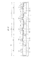
 diffusion prevention regions 10a and 10b) is not only a semiconductor device having a CMISFET, but also a semiconductor device having only one of a p-channel MISFET and an n-channel MISFET. However, if applied to a semiconductor device having at least an n-channel MISFET, the effect is great. The same applies to the following second to sixth embodiments.

(実施の形態2)
本実施の形態2の半導体装置の製造工程を図面を参照して説明する。図16〜図22は、本実施の形態の半導体装置の製造工程中の要部断面図である。
(Embodiment 2)
A manufacturing process of the semiconductor device according to the second embodiment will be described with reference to the drawings. 16 to 22 are main-portion cross-sectional views during the manufacturing process of the semiconductor device of the present embodiment.

本実施の形態では、まず、図16に示されるように、例えば1〜10Ωcm程度の比抵抗を有するp型の単結晶シリコンなどからなる半導体基板(半導体ウエハ)1aを準備し、半導体基板1a(の主面全面)上に半導体層(半導体領域)1bを形成する。   In the present embodiment, first, as shown in FIG. 16, a semiconductor substrate (semiconductor wafer) 1a made of p-type single crystal silicon having a specific resistance of about 1 to 10 Ωcm, for example, is prepared, and the semiconductor substrate 1a ( A semiconductor layer (semiconductor region) 1b is formed on the entire main surface of the substrate.

半導体層1bは、炭素(C)、窒素(N)またはフッ素(F)のうちの1種以上(すなわち第1元素)が導入された半導体層(単結晶シリコン層)であり、具体的には、炭素(C)、窒素(N)またはフッ素(F)のうちの1種以上(すなわち第1元素)が導入(ドープ)された単結晶シリコン(Si)で構成されている。   The semiconductor layer 1b is a semiconductor layer (single crystal silicon layer) into which one or more of carbon (C), nitrogen (N), or fluorine (F) (ie, the first element) is introduced. , Carbon (C), nitrogen (N), or fluorine (F) is made of single crystal silicon (Si) into which one or more (that is, the first element) are introduced (doped).

半導体層1bは、好ましくは、半導体基板1a上に半導体層1bをエピタキシャル成長させることで形成されている。半導体基板1aとその上の半導体層1bとを合わせたものを、半導体基板SUB1と称することとし、この半導体基板SUB1は、いわゆるエピタキシャルウエハとみなすこともできる。半導体基板SUB1の主面(表面)は、半導体層1bの主面(表面)に対応する。半導体層1bにおける第1元素の濃度は、例えば1×10¹⁸〜1×10²⁰/cm程度とすることができる。半導体層1bの厚さは、後で形成されるp型ウエルPWおよびn型ウエルNWが半導体層1b内に含まれ得るような厚さで形成され、例えば1〜10μm程度の厚さを有している。 The semiconductor layer 1b is preferably formed by epitaxially growing the semiconductor layer 1b on the semiconductor substrate 1a. A combination of the semiconductor substrate 1a and the semiconductor layer 1b thereon is referred to as a semiconductor substrate SUB1, and the semiconductor substrate SUB1 can also be regarded as a so-called epitaxial wafer. The main surface (front surface) of the semiconductor substrate SUB1 corresponds to the main surface (front surface) of the semiconductor layer 1b. The concentration of the first element in the semiconductor layer 1b can be, for example, about 1 × 10 18 to 1 × 10 20 / cm 3 . The thickness of the semiconductor layer 1b is formed such that a p-type well PW and an n-type well NW to be formed later can be included in the semiconductor layer 1b, and has a thickness of, for example, about 1 to 10 μm. ing.

他の形態として、炭素(C)、窒素(N)またはフッ素(F)のうちの1種以上が導入された半導体層(半導体領域)1bを、半導体基板1aの上層部分に炭素(C)、窒素(N)またはフッ素(F)のうちの1種以上をイオン注入することによって形成することもできる。   As another form, a semiconductor layer (semiconductor region) 1b into which one or more of carbon (C), nitrogen (N), or fluorine (F) are introduced is formed on the upper layer portion of the semiconductor substrate 1a with carbon (C), It can also be formed by ion implantation of one or more of nitrogen (N) or fluorine (F).

次に、図17に示されるように、半導体基板SUB1の主面に素子分離領域2を形成する。素子分離領域2の形成法などは、上記実施の形態1と同様であるので、ここではその説明は省略する。素子分離領域2によって、nMIS形成領域1AとpMIS形成領域1Bとが規定される。   Next, as shown in FIG. 17, the element isolation region 2 is formed on the main surface of the semiconductor substrate SUB1. Since the method for forming the element isolation region 2 is the same as that in the first embodiment, the description thereof is omitted here. The element isolation region 2 defines an nMIS formation region 1A and a pMIS formation region 1B.

次に、上記実施の形態1と同様の絶縁膜3を半導体基板SUB1の表面(すなわち半導体層1bの表面)に形成する。   Next, an insulating film 3 similar to that of the first embodiment is formed on the surface of the semiconductor substrate SUB1 (that is, the surface of the semiconductor layer 1b).

次に、図18に示されるように、nMIS形成領域1Aにおいて、上記実施の形態1のチャネルドープイオン注入IM1aと同様のチャネルドープイオン注入(後で形成されるnチャネル型MISFETQnのしきい値調整用のイオン注入)IM1aを行なって、半導体層1bの上層部分にチャネルドープ層4aを形成する。それから、nMIS形成領域1Aにおいて、半導体層1bにp型ウエルPWをイオン注入によって形成する。また、pMIS形成領域1Bにおいて、上記実施の形態1のチャネルドープイオン注入IM1bと同様のチャネルドープイオン注入(後で形成されるpチャネル型MISFETQpのしきい値調整用のイオン注入)IM1bを行なって、半導体層1bの上層部分にチャネルドープ層4bを形成する。それから、pMIS形成領域1Bにおいて、半導体層1bにn型ウエルNWをイオン注入によって形成する。   Next, as shown in FIG. 18, in the nMIS formation region 1A, channel doping ion implantation similar to the channel doping ion implantation IM1a of the first embodiment (threshold adjustment of the n channel MISFET Qn formed later) (Ion implantation) IM1a is performed to form a channel dope layer 4a in the upper layer portion of the semiconductor layer 1b. Then, in the nMIS formation region 1A, a p-type well PW is formed in the semiconductor layer 1b by ion implantation. Further, in the pMIS formation region 1B, channel doping ion implantation (ion implantation for adjusting the threshold value of a p-channel type MISFET Qp formed later) IM1b similar to the channel doping ion implantation IM1b of the first embodiment is performed. The channel dope layer 4b is formed in the upper layer portion of the semiconductor layer 1b. Then, in the pMIS formation region 1B, an n-type well NW is formed in the semiconductor layer 1b by ion implantation.

なお、図18では、チャネルドープイオン注入IM1a,IM1bを矢印で模式的に示してあるが、チャネルドープイオン注入IM1aとチャネルドープイオン注入IM1bとは、それぞれ別工程で行なう。すなわち、上記実施の形態1と同様に本実施の形態においても、チャネルドープ層4aを形成するためのチャネルドープイオン注入IM1aと、p型ウエルPWを形成するためのイオン注入とは、上記フォトレジスト膜RP1aと同様のフォトレジスト膜(図示せず)でpMIS形成領域1Bを覆った状態で行ない、pMIS形成領域1Bの半導体層1bにイオン注入されないようにする。一方、チャネルドープ層4bを形成するためのチャネルドープイオン注入IM1bと、n型ウエルNWを形成するためのイオン注入とは、上記フォトレジスト膜RP1bと同様のフォトレジスト膜(図示せず)でnMIS形成領域1Aを覆った状態で行ない、nMIS形成領域1Aの半導体層1bにイオン注入されないようにする。   In FIG. 18, channel dope ion implantation IM1a and IM1b are schematically indicated by arrows, but channel dope ion implantation IM1a and channel dope ion implantation IM1b are performed in separate steps. That is, in the present embodiment as in the first embodiment, the channel dope ion implantation IM1a for forming the channel dope layer 4a and the ion implantation for forming the p-type well PW are the same as those in the photoresist. The pMIS formation region 1B is covered with a photoresist film (not shown) similar to the film RP1a so that ions are not implanted into the semiconductor layer 1b in the pMIS formation region 1B. On the other hand, the channel dope ion implantation IM1b for forming the channel dope layer 4b and the ion implantation for forming the n-type well NW are performed by a photoresist film (not shown) similar to the photoresist film RP1b in the nMIS. The process is performed while covering the formation region 1A so that ions are not implanted into the semiconductor layer 1b in the nMIS formation region 1A.

上記実施の形態1では、半導体基板1にチャネルドープイオン注入IM1a,IM1bを行なってチャネルドープ層4a,4bを形成していた。それに対して、本実施の形態では、半導体層1bにチャネルドープイオン注入IM1a,IM1bを行なってチャネルドープ層4a,4bを形成しているが、それ以外は、本実施の形態でのチャネルドープイオン注入IM1a,IM1bおよびチャネルドープ層4a,4bの構成については、上記実施の形態1と同様である。また、上記実施の形態1では、半導体基板1にp型ウエルPWおよびn型ウエルNWを形成していたのに対して、本実施の形態では、半導体層1bにp型ウエルPWおよびn型ウエルNWを形成しているが、それ以外は、本実施の形態でのp型ウエルPWおよびn型ウエルNWの形成法と構成については、上記実施の形態1と同様である。   In the first embodiment, channel dope ion implantation IM1a and IM1b are performed on the semiconductor substrate 1 to form the channel dope layers 4a and 4b. In contrast, in this embodiment, channel dope ion implantation IM1a and IM1b are performed in the semiconductor layer 1b to form channel dope layers 4a and 4b. Otherwise, the channel dope ions in the present embodiment are used. The configurations of the implantations IM1a and IM1b and the channel dope layers 4a and 4b are the same as those in the first embodiment. In the first embodiment, the p-type well PW and the n-type well NW are formed in the semiconductor substrate 1, whereas in the present embodiment, the p-type well PW and the n-type well are formed in the semiconductor layer 1b. The NW is formed, but other than that, the formation method and configuration of the p-type well PW and the n-type well NW in the present embodiment are the same as those in the first embodiment.

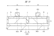
次に、上記絶縁膜3を除去して半導体層1bの表面を清浄化した後、nMIS形成領域1AおよびpMIS形成領域1Bの半導体層1bの表面(p型ウエルPWおよびn型ウエルNWの表面)上にゲート絶縁膜用の絶縁膜5を形成する。上記実施の形態1では、半導体基板1に絶縁膜の表面に絶縁膜5を形成していたのに対して、本実施の形態では、半導体層1bに絶縁膜5を形成しているが、それ以外は、本実施の形態での絶縁膜5の形成法と構成については、上記実施の形態1と同様である。   Next, after removing the insulating film 3 to clean the surface of the semiconductor layer 1b, the surface of the semiconductor layer 1b in the nMIS formation region 1A and the pMIS formation region 1B (surfaces of the p-type well PW and the n-type well NW). An insulating film 5 for a gate insulating film is formed thereon. In the first embodiment, the insulating film 5 is formed on the surface of the insulating film on the semiconductor substrate 1, whereas in the present embodiment, the insulating film 5 is formed on the semiconductor layer 1b. Except for the above, the formation method and configuration of the insulating film 5 in the present embodiment are the same as those in the first embodiment.

次に、ゲート電極GE1,GE2を形成する。上記実施の形態1では、半導体基板1上に絶縁膜5(ゲート絶縁膜5a,5b)を介してゲート電極GE1,GE2を形成していたのに対して、本実施の形態では、半導体層1b上に絶縁膜5(ゲート絶縁膜5a,5b)を介してゲート電極GE1,GE2を形成している。それ以外は、本実施の形態でのゲート電極GE1,GE2の形成法と構成については、上記実施の形態1と同様である。これにより、図19の構造が得られる。   Next, gate electrodes GE1 and GE2 are formed. In the first embodiment, the gate electrodes GE1 and GE2 are formed on the semiconductor substrate 1 via the insulating film 5 (gate insulating films 5a and 5b), whereas in the present embodiment, the semiconductor layer 1b is formed. Gate electrodes GE1 and GE2 are formed thereon via an insulating film 5 (gate insulating films 5a and 5b). Other than that, the formation method and configuration of the gate electrodes GE1 and GE2 in the present embodiment are the same as those in the first embodiment. Thereby, the structure of FIG. 19 is obtained.

次に、図20に示されるように、nMIS形成領域1Aの半導体層1b(p型ウエルPW)のゲート電極GE1の両側の領域に、リン(P)またはヒ素(As)などのn型の不純物をイオン注入することにより、エクステンション領域7aを形成する。それから、nMIS形成領域1Aの半導体層1b(p型ウエルPW)に、イオン注入(ハローイオン注入)を行ってハロー領域8aを形成する。また、pMIS形成領域1Bの半導体層1b(n型ウエルNW)のゲート電極GE2の両側の領域に、上記実施の形態1と同様に、ホウ素(B)などのp型の不純物をイオン注入することにより、エクステンション領域7bを形成する。それから、pMIS形成領域1Bの半導体層1b(n型ウエルNW)に、イオン注入(ハローイオン注入)を行ってハロー領域8bを形成する。   Next, as shown in FIG. 20, n-type impurities such as phosphorus (P) or arsenic (As) are formed in the regions on both sides of the gate electrode GE1 of the semiconductor layer 1b (p-type well PW) in the nMIS formation region 1A. Then, the extension region 7a is formed. Then, ion implantation (halo ion implantation) is performed on the semiconductor layer 1b (p-type well PW) in the nMIS formation region 1A to form the halo region 8a. Also, a p-type impurity such as boron (B) is ion-implanted into the regions on both sides of the gate electrode GE2 of the semiconductor layer 1b (n-type well NW) in the pMIS formation region 1B, as in the first embodiment. Thus, the extension region 7b is formed. Then, ion implantation (halo ion implantation) is performed on the semiconductor layer 1b (n-type well NW) in the pMIS formation region 1B to form the halo region 8b.

なお、上記実施の形態1と同様に本実施の形態2および以下の実施の形態3,4においても、エクステンション領域7aを形成するためのイオン注入と、ハロー領域8aを形成するためのイオン注入とは、上記フォトレジスト膜RP2aと同様のフォトレジスト膜(図示せず)でpMIS形成領域1Bを覆った状態で行ない、pMIS形成領域1Bの半導体層1bにイオン注入されないようにする。一方、上記実施の形態1と同様に本実施の形態2および以下の実施の形態3,4においても、エクステンション領域7bを形成するためのイオン注入と、ハロー領域8bを形成するためのイオン注入とは、上記フォトレジスト膜RP2bと同様のフォトレジスト膜(図示せず)でnMIS形成領域1Aを覆った状態で行ない、nMIS形成領域1Aの半導体層1bにイオン注入されないようにする。   As in the first embodiment, also in the second embodiment and the following third and fourth embodiments, ion implantation for forming the extension region 7a and ion implantation for forming the halo region 8a Is performed in a state where the pMIS formation region 1B is covered with a photoresist film (not shown) similar to the photoresist film RP2a so that ions are not implanted into the semiconductor layer 1b in the pMIS formation region 1B. On the other hand, in the second embodiment and the following third and fourth embodiments as in the first embodiment, the ion implantation for forming the extension region 7b and the ion implantation for forming the halo region 8b The nMIS formation region 1A is covered with a photoresist film (not shown) similar to the photoresist film RP2b so that ions are not implanted into the semiconductor layer 1b in the nMIS formation region 1A.

上記実施の形態1では、半導体基板1にエクステンション領域7a,7bおよびハロー領域8a,8bを形成していたのに対して、本実施の形態では、半導体層1bにエクステンション領域7a,7bおよびハロー領域8a,8bを形成しているが、それ以外は、本実施の形態でのエクステンション領域7a,7bおよびハロー領域8a,8bの形成法と構成については、上記実施の形態1と同様である。   In the first embodiment, the extension regions 7a and 7b and the halo regions 8a and 8b are formed in the semiconductor substrate 1, whereas in the present embodiment, the extension regions 7a and 7b and the halo region are formed in the semiconductor layer 1b. 8a and 8b are formed. Otherwise, the formation method and configuration of the extension regions 7a and 7b and the halo regions 8a and 8b in the present embodiment are the same as those in the first embodiment.

次に、図21に示されるように、上記実施の形態1と同様に、ゲート電極GE1,GE2の側壁上にサイドウォール(側壁絶縁膜)SWを形成する。   Next, as shown in FIG. 21, as in the first embodiment, sidewalls (sidewall insulating films) SW are formed on the sidewalls of the gate electrodes GE1 and GE2.

次に、nMIS形成領域1Aの半導体層1b(p型ウエルPW)のゲート電極GE1およびサイドウォールSWの両側の領域に、リン(P)またはヒ素(As)などのn型の不純物をイオン注入することにより、n型半導体領域11a(ソース、ドレイン)を形成する。また、pMIS形成領域1Bの半導体層1b(n型ウエルNW)のゲート電極GE2およびサイドウォールSWの両側の領域に、ホウ素(B)などのp型の不純物をイオン注入することにより、p型半導体領域11b(ソース、ドレイン)を形成する。 Next, n-type impurities such as phosphorus (P) or arsenic (As) are ion-implanted into the regions on both sides of the gate electrode GE1 and the sidewall SW of the semiconductor layer 1b (p-type well PW) in the nMIS formation region 1A. Thus, the n + type semiconductor region 11a (source, drain) is formed. Further, p + type impurities such as boron (B) are ion-implanted into regions on both sides of the gate electrode GE2 and the sidewall SW of the semiconductor layer 1b (n-type well NW) in the pMIS formation region 1B. A semiconductor region 11b (source, drain) is formed.

なお、上記実施の形態1と同様に本実施の形態2および以下の実施の形態3,4においても、n型半導体領域11aを形成するためのイオン注入は、上記フォトレジスト膜RP3aと同様のフォトレジスト膜(図示せず)でpMIS形成領域1Bを覆った状態で行ない、pMIS形成領域1Bの半導体層1bにイオン注入されないようにする。一方、上記実施の形態1と同様に本実施の形態2および以下の実施の形態3,4においても、p型半導体領域11bを形成するためのイオン注入は、上記フォトレジスト膜RP3bと同様のフォトレジスト膜(図示せず)でnMIS形成領域1Aを覆った状態で行ない、nMIS形成領域1Aの半導体層1bにイオン注入されないようにする。 As in the first embodiment, also in the second embodiment and the following third and fourth embodiments, the ion implantation for forming the n + type semiconductor region 11a is the same as that in the photoresist film RP3a. The pMIS formation region 1B is covered with a photoresist film (not shown) so that ions are not implanted into the semiconductor layer 1b in the pMIS formation region 1B. On the other hand, in the second embodiment and the following third and fourth embodiments as in the first embodiment, the ion implantation for forming the p + type semiconductor region 11b is the same as that in the photoresist film RP3b. The nMIS formation region 1A is covered with a photoresist film (not shown) so that ions are not implanted into the semiconductor layer 1b in the nMIS formation region 1A.

上記実施の形態1では、半導体基板1にn型半導体領域11aおよびp型半導体領域11bを形成していたのに対して、本実施の形態では、半導体層1bにn型半導体領域11aおよびp型半導体領域11bを形成しているが、それ以外は、本実施の形態でのn型半導体領域11aおよびp型半導体領域11bの形成法と構成については、上記実施の形態1と同様である。 In the first embodiment, the n + type semiconductor region 11a and the p + type semiconductor region 11b are formed in the semiconductor substrate 1, whereas in the present embodiment, the n + type semiconductor region 11a is formed in the semiconductor layer 1b. The p + -type semiconductor region 11b is formed. Otherwise, the formation method and configuration of the n + -type semiconductor region 11a and the p + -type semiconductor region 11b in the present embodiment are described in the first embodiment. It is the same.

次に、上記実施の形態1と同様に、これまでのイオン注入で導入した不純物の活性化のためのアニール処理(熱処理)を行う。   Next, similarly to the first embodiment, annealing treatment (heat treatment) for activating the impurities introduced by the conventional ion implantation is performed.

以降の工程は、上記実施の形態1と同様である。すなわち、図22に示されるように、ゲート電極GE1,GE2、n型半導体領域11aおよびp型半導体領域11bの表面にそれぞれ金属シリサイド層12を形成し、半導体基板SUB1の主面(すなわち半導体層1bの主面)上にゲート電極GE1,GE2を覆うように絶縁膜21を形成し、絶縁膜21上に絶縁膜22を形成する。それから、絶縁膜22,21にコンタクトホール23を形成し、コンタクトホール23内にプラグ24を形成する。その後、プラグ24が埋め込まれた絶縁膜22上に、ストッパ絶縁膜25および絶縁膜26を順に形成し、絶縁膜26およびストッパ絶縁膜25に配線溝27を形成し、配線溝27の底部および側壁上を含む絶縁膜26上にバリア導体膜28を形成し、配線溝27を銅の主導体膜29で埋め込んで配線M1を形成する。 The subsequent steps are the same as those in the first embodiment. That is, as shown in FIG. 22, the metal silicide layers 12 are formed on the surfaces of the gate electrodes GE1, GE2, the n + type semiconductor region 11a and the p + type semiconductor region 11b, respectively, and the main surface of the semiconductor substrate SUB1 (that is, the semiconductor) An insulating film 21 is formed on the main surface of the layer 1b so as to cover the gate electrodes GE1 and GE2, and an insulating film 22 is formed on the insulating film 21. Then, contact holes 23 are formed in the insulating films 22 and 21, and plugs 24 are formed in the contact holes 23. Thereafter, a stopper insulating film 25 and an insulating film 26 are sequentially formed on the insulating film 22 in which the plug 24 is embedded, a wiring groove 27 is formed in the insulating film 26 and the stopper insulating film 25, and the bottom and side walls of the wiring groove 27 are formed. A barrier conductor film 28 is formed on the insulating film 26 including the upper portion, and the wiring groove 27 is filled with a copper main conductor film 29 to form a wiring M1.

次に、本実施の形態の効果について、より詳細に説明する。   Next, the effect of this embodiment will be described in more detail.

上記実施の形態1では、炭素(C)、窒素(N)またはフッ素(F)のうちの1種以上が導入された拡散防止領域10a,10bを形成することで、チャネル領域への点欠陥の拡散を防止し、それによって、チャネル領域における点欠陥の密度を抑制して、チャネルドープイオン注入でチャネル領域に導入された不純物の再配置(拡散)を抑制していた。   In the first embodiment, by forming the diffusion prevention regions 10a and 10b into which at least one of carbon (C), nitrogen (N), and fluorine (F) is introduced, the point defects in the channel region are reduced. Diffusion was prevented, thereby suppressing the density of point defects in the channel region, and relocation (diffusion) of impurities introduced into the channel region by channel doping ion implantation was suppressed.

それに対して、本実施の形態では、炭素(C)、窒素(N)またはフッ素(F)のうちの1種以上が導入された半導体層1bを上部に有する半導体基板SUB1を準備し、この半導体層1bにnチャネル型MISFETQnおよびpチャネル型MISFETQpを形成している。すなわち、本実施の形態では、nチャネル型MISFETQnおよびpチャネル型MISFETQpのチャネル領域、エクステンション領域7a,7b、ハロー領域8a,8b、n型半導体領域11aおよびp型半導体領域11bは、炭素(C)、窒素(N)またはフッ素(F)のうちの1種以上が導入された半導体層1bに形成されている。 On the other hand, in the present embodiment, a semiconductor substrate SUB1 having a semiconductor layer 1b into which one or more of carbon (C), nitrogen (N), and fluorine (F) are introduced is prepared. An n-channel MISFET Qn and a p-channel MISFET Qp are formed in the layer 1b. That is, in the present embodiment, the channel region, extension regions 7a and 7b, halo regions 8a and 8b, n + type semiconductor region 11a and p + type semiconductor region 11b of the n channel MISFET Qn and p channel MISFET Qp are made of carbon ( C), formed in the semiconductor layer 1b into which one or more of nitrogen (N) and fluorine (F) are introduced.

上述のように、単結晶シリコンに炭素(C)、窒素(N)またはフッ素(F)のうちの1種以上が導入された領域(本実施の形態の半導体層1bに対応)は、点欠陥が拡散(移動)しにくく、点欠陥の拡散(移動)を防止する機能を有している。このため、本実施の形態では、炭素(C)、窒素(N)またはフッ素(F)のうちの1種以上が導入された半導体層1b全体に渡って、点欠陥が拡散(移動)しにくい。このため、エクステンション領域7a,7b、ハロー領域8a,8b、n型半導体領域11aおよびp型半導体領域11bを形成する際の各イオン注入で生成された点欠陥が、nチャネル型MISFETQnおよびpチャネル型MISFETQpのチャネル領域(ゲート電極GE1,GE2の直下の領域)にまで拡散するのを防止でき、チャネル領域における点欠陥の密度を抑制することできる。これにより、チャネルドープイオン注入でチャネル領域に導入された不純物が、その後の加熱工程の際に再配置(拡散)されるのを抑制または防止することができるので、注入直後のチャネルドープ不純物の配置(ランダム性が高い配置)を維持することができる。従って、MISFET毎のチャネル領域の状態(不純物分布)のばらつきを抑制して、MISFET毎のしきい値電圧のばらつきを抑制することができ、半導体装置の性能を向上させることができる。 As described above, a region where one or more of carbon (C), nitrogen (N), and fluorine (F) is introduced into single crystal silicon (corresponding to the semiconductor layer 1b in this embodiment) is a point defect. Is difficult to diffuse (move) and has a function of preventing the diffusion (movement) of point defects. For this reason, in this embodiment, point defects hardly diffuse (move) over the entire semiconductor layer 1b into which one or more of carbon (C), nitrogen (N), and fluorine (F) are introduced. . For this reason, the point defects generated by the respective ion implantations when forming the extension regions 7a and 7b, the halo regions 8a and 8b, the n + type semiconductor region 11a and the p + type semiconductor region 11b are converted into n channel type MISFETs Qn and p. Diffusion to the channel region of the channel type MISFET Qp (region immediately below the gate electrodes GE1 and GE2) can be prevented, and the density of point defects in the channel region can be suppressed. As a result, it is possible to suppress or prevent the impurities introduced into the channel region by the channel doping ion implantation from being rearranged (diffused) during the subsequent heating step. (Arrangement with high randomness) can be maintained. Therefore, variations in channel region states (impurity distribution) for each MISFET can be suppressed, variations in threshold voltage for each MISFET can be suppressed, and the performance of the semiconductor device can be improved.

また、半導体層1bには、炭素(C)、窒素(N)またはフッ素(F)のうちの1種以上が導入されているが、炭素(C)、窒素(N)およびフッ素(F)のうち、点欠陥の拡散防止に最も有効なのは炭素(C)である。このため、半導体層1bには、炭素(C)、窒素(N)またはフッ素(F)のうち少なくとも炭素(C)を導入していればより好ましい。   In addition, one or more of carbon (C), nitrogen (N), and fluorine (F) are introduced into the semiconductor layer 1b, but carbon (C), nitrogen (N), and fluorine (F) Of these, carbon (C) is most effective in preventing the diffusion of point defects. For this reason, it is more preferable that at least carbon (C) is introduced into the semiconductor layer 1b among carbon (C), nitrogen (N), or fluorine (F).

また、本実施の形態では、半導体基板1aの主面上に半導体層1bをエピタキシャル成長などで形成したが、他の形態として、半導体基板1の上層部分に炭素(C)、窒素(N)またはフッ素(F)のうちの1種以上をイオン注入することで、半導体基板1の上層部分に半導体層1bに相当する領域を形成することもできる。この場合、上記半導体基板SUB1全体が上記半導体基板1に相当し、上記半導体基板SUB1のうちの上記半導体層1bが、半導体基板1のうち、イオン注入で炭素(C)、窒素(N)またはフッ素(F)のうちの1種以上を導入した半導体領域(半導体層)に相当する。すなわち、半導体基板1の上層部分に炭素(C)、窒素(N)またはフッ素(F)のうちの1種以上をイオン注入することで、半導体層1bに相当する半導体領域(半導体層)を形成し、この半導体領域(半導体層)内に、p型ウエルPW、n型ウエルNW、エクステンション領域7a,7b、ハロー領域8a,8b、n型半導体領域11aおよびp型半導体領域11bを形成するのである。この場合も、エクステンション領域7a,7b、ハロー領域8a,8b、n型半導体領域11aおよびp型半導体領域11bを形成する際のイオン注入で生成された点欠陥が、nチャネル型MISFETQnおよびpチャネル型MISFETQpのチャネル領域に拡散するのを防止でき、チャネル領域における点欠陥の密度を抑制することができる。従って、チャネルドープイオン注入でチャネル領域に導入された不純物が、その後の加熱工程の際に再配置(拡散)されるのを抑制または防止することができ、MISFET毎のチャネル領域の状態(不純物分布)のばらつきを抑制して、MISFET毎のしきい値電圧のばらつきを抑制することができる。 In the present embodiment, the semiconductor layer 1b is formed on the main surface of the semiconductor substrate 1a by epitaxial growth or the like. However, as another form, carbon (C), nitrogen (N) or fluorine is formed on the upper layer portion of the semiconductor substrate 1. A region corresponding to the semiconductor layer 1b can be formed in the upper layer portion of the semiconductor substrate 1 by ion-implanting one or more of (F). In this case, the entire semiconductor substrate SUB1 corresponds to the semiconductor substrate 1, and the semiconductor layer 1b of the semiconductor substrate SUB1 is carbon (C), nitrogen (N) or fluorine by ion implantation in the semiconductor substrate 1. This corresponds to a semiconductor region (semiconductor layer) into which one or more of (F) are introduced. That is, a semiconductor region (semiconductor layer) corresponding to the semiconductor layer 1b is formed by ion-implanting one or more of carbon (C), nitrogen (N), or fluorine (F) into the upper layer portion of the semiconductor substrate 1. Then, the p-type well PW, the n-type well NW, the extension regions 7a and 7b, the halo regions 8a and 8b, the n + type semiconductor region 11a and the p + type semiconductor region 11b are formed in the semiconductor region (semiconductor layer). It is. Also in this case, the point defects generated by the ion implantation when forming the extension regions 7a and 7b, the halo regions 8a and 8b, the n + type semiconductor region 11a and the p + type semiconductor region 11b are the n channel type MISFETs Qn and p. Diffusion into the channel region of the channel type MISFET Qp can be prevented, and the density of point defects in the channel region can be suppressed. Therefore, it is possible to suppress or prevent the impurities introduced into the channel region by channel doping ion implantation from being rearranged (diffused) during the subsequent heating process, and the state of the channel region (impurity distribution) for each MISFET. ) Can be suppressed, and variations in threshold voltage for each MISFET can be suppressed.

また、本実施の形態では、半導体層1b全体に炭素(C)、窒素(N)またはフッ素(F)のうちの1種以上を導入して、そこにp型ウエルPW、n型ウエルNW、エクステンション領域7a,7b、ハロー領域8a,8b、n型半導体領域11aおよびp型半導体領域11bを形成している。このため、炭素(C)、窒素(N)またはフッ素(F)のうちの1種以上を導入したことによる、イオン注入時に生成された点欠陥の拡散を抑制する効果は、極めて大きい。 In the present embodiment, at least one of carbon (C), nitrogen (N), and fluorine (F) is introduced into the entire semiconductor layer 1b, and p-type well PW, n-type well NW, Extension regions 7a and 7b, halo regions 8a and 8b, an n + type semiconductor region 11a and a p + type semiconductor region 11b are formed. For this reason, the effect which suppresses the spreading | diffusion of the point defect produced | generated at the time of ion implantation by introduce | transducing 1 or more types of carbon (C), nitrogen (N), or fluorine (F) is very large.

(実施の形態3)
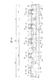
本実施の形態3の半導体装置の製造工程を図面を参照して説明する。図23〜図32は、本実施の形態の半導体装置の製造工程中の要部断面図である。
(Embodiment 3)
A manufacturing process of the semiconductor device according to the third embodiment will be described with reference to the drawings. 23 to 32 are main-portion cross-sectional views during the manufacturing process of the semiconductor device of the present embodiment.

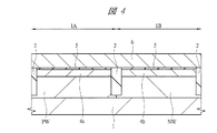
本実施の形態では、上記実施の形態1と同様に、図23に示されるように、まず、半導体基板(半導体ウエハ)1を準備し、半導体基板1の主面に素子分離領域2を形成する。   In the present embodiment, as in the first embodiment, as shown in FIG. 23, first, a semiconductor substrate (semiconductor wafer) 1 is prepared, and an element isolation region 2 is formed on the main surface of the semiconductor substrate 1. .

次に、上記実施の形態1と同様の絶縁膜3を半導体基板1の表面に形成する。   Next, an insulating film 3 similar to that of the first embodiment is formed on the surface of the semiconductor substrate 1.

次に、nMIS形成領域1Aにおいて、上記実施の形態1と同様にして、半導体基板1の主面から所定の深さに渡ってp型ウエルPWを形成し、また、pMIS形成領域1Bにおいて、上記実施の形態1と同様にして、半導体基板1の主面から所定の深さに渡ってn型ウエルNWを形成する。本実施の形態でのp型ウエルPWおよびn型ウエルNWの形成法と構成については、上記実施の形態1と同様である。   Next, in the nMIS formation region 1A, a p-type well PW is formed from the main surface of the semiconductor substrate 1 to a predetermined depth in the same manner as in the first embodiment. In the pMIS formation region 1B, In the same manner as in the first embodiment, an n-type well NW is formed from the main surface of the semiconductor substrate 1 to a predetermined depth. The formation method and configuration of the p-type well PW and the n-type well NW in the present embodiment are the same as those in the first embodiment.

なお、本実施の形態では、後述するゲート絶縁膜用の絶縁膜5を形成する前には、nチャネル型MISFETQnのしきい値調整用のチャネルドープイオン注入IM1aおよびpチャネル型MISFETQpのしきい値調整用のチャネルドープイオン注入IM1bは行なわないため、この段階では、チャネルドープ層4a,4bは形成されていない。   In this embodiment, before forming an insulating film 5 for a gate insulating film, which will be described later, the threshold value of the channel dope ion implantation IM1a for adjusting the threshold value of the n-channel type MISFET Qn and the threshold value of the p-channel type MISFET Qp. Since channel doping ion implantation IM1b for adjustment is not performed, channel doped layers 4a and 4b are not formed at this stage.

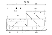
次に、図24に示されるように、上記実施の形態1と同様、上記絶縁膜3を除去して半導体基板1の表面を清浄化した後、nMIS形成領域1AおよびpMIS形成領域1Bの半導体基板1の表面(p型ウエルPWおよびn型ウエルNWの表面)上にゲート絶縁膜用の絶縁膜5を形成する。本実施の形態での絶縁膜5の形成法と構成については、上記実施の形態1と同様である。   Next, as shown in FIG. 24, after removing the insulating film 3 and cleaning the surface of the semiconductor substrate 1 as in the first embodiment, the semiconductor substrates in the nMIS formation region 1A and the pMIS formation region 1B An insulating film 5 for a gate insulating film is formed on the surface of 1 (the surfaces of the p-type well PW and the n-type well NW). The formation method and configuration of the insulating film 5 in the present embodiment are the same as those in the first embodiment.

次に、図25に示されるように、半導体基板1の主面全面上(すなわちnMIS形成領域1AおよびpMIS形成領域1Bの絶縁膜5上を含む)に、導電体膜(導電体層)として、多結晶シリコン膜のようなシリコン膜(第1導電体層)6aを形成する。また、シリコン膜6aは、成膜時にはアモルファスシリコン膜であったものを、成膜後の熱処理により多結晶シリコン膜に変えることもできる。シリコン膜6aの厚み(堆積膜厚)t1は、例えば20〜100nm程度とすることができる。   Next, as shown in FIG. 25, as a conductor film (conductor layer) on the entire main surface of the semiconductor substrate 1 (that is, on the insulating film 5 of the nMIS formation region 1A and the pMIS formation region 1B), A silicon film (first conductor layer) 6a such as a polycrystalline silicon film is formed. Further, the silicon film 6a, which was an amorphous silicon film at the time of film formation, can be changed to a polycrystalline silicon film by heat treatment after the film formation. The thickness (deposited film thickness) t1 of the silicon film 6a can be set to, for example, about 20 to 100 nm.

次に、図26に示されるように、pMIS形成領域1Bを覆うフォトレジスト膜(フォトレジストパターン)RP4aを、フォトリソグラフィ技術を用いて形成する。nMIS形成領域1Aは、このフォトレジスト膜RP4aでは覆われずに露出される。このフォトレジスト膜RP4aは、pMIS形成領域1Bへのイオン注入阻止マスクとして機能することができる。   Next, as shown in FIG. 26, a photoresist film (photoresist pattern) RP4a covering the pMIS formation region 1B is formed by using a photolithography technique. The nMIS formation region 1A is exposed without being covered with the photoresist film RP4a. The photoresist film RP4a can function as an ion implantation blocking mask for the pMIS formation region 1B.

次に、nMIS形成領域1Aにおいて、上記実施の形態1と同様のチャネルドープイオン注入(後で形成されるnチャネル型MISFETQnのしきい値調整用のイオン注入)IM1aを行なって、半導体基板1(p型ウエルPW)の上層部分にチャネルドープ層4aを形成する。なお、図26では、チャネルドープイオン注入IM1aを矢印で模式的に示してある。   Next, in the nMIS formation region 1A, channel doping ion implantation (ion implantation for adjusting the threshold value of an n-channel MISFET Qn to be formed later) IM1a similar to that in the first embodiment is performed, and the semiconductor substrate 1 ( A channel dope layer 4a is formed in the upper layer portion of the p-type well PW). In FIG. 26, the channel dope ion implantation IM1a is schematically indicated by an arrow.

上記実施の形態1では、ゲート絶縁膜用の絶縁膜5の形成前に半導体基板1にチャネルドープイオン注入IM1aを行なってチャネルドープ層4aを形成していた。これに対して、本実施の形態では、ゲート絶縁膜用の絶縁膜5とシリコン膜6aの形成後にチャネルドープイオン注入IM1aを行なってチャネルドープ層4aを形成しているが、それ以外は、本実施の形態でのチャネルドープイオン注入IM1aおよびチャネルドープ層4aの構成については、上記実施の形態1と同様である。   In the first embodiment, the channel dope ion implantation IM1a is performed on the semiconductor substrate 1 before forming the insulating film 5 for the gate insulating film to form the channel dope layer 4a. On the other hand, in this embodiment, the channel dope ion implantation IM1a is performed after the formation of the insulating film 5 for the gate insulating film and the silicon film 6a to form the channel dope layer 4a. The configurations of the channel dope ion implantation IM1a and the channel dope layer 4a in the embodiment are the same as those in the first embodiment.

次に、図27に示されるように、フォトレジスト膜RP4aを除去してから、nMIS形成領域1Aを覆うフォトレジスト膜(フォトレジストパターン)RP4bを、フォトリソグラフィ技術を用いて形成する。pMIS形成領域1Bは、このフォトレジスト膜RP4bでは覆われずに露出される。このフォトレジスト膜RP4bは、nMIS形成領域1Aへのイオン注入阻止マスクとして機能することができる。   Next, as shown in FIG. 27, after the photoresist film RP4a is removed, a photoresist film (photoresist pattern) RP4b covering the nMIS formation region 1A is formed by using a photolithography technique. The pMIS formation region 1B is exposed without being covered with the photoresist film RP4b. The photoresist film RP4b can function as an ion implantation blocking mask for the nMIS formation region 1A.

次に、pMIS形成領域1Bにおいて、上記実施の形態1と同様のチャネルドープイオン注入(後で形成されるpチャネル型MISFETQpのしきい値調整用のイオン注入)IM1bを行なって、半導体基板1(n型ウエルNW)の上層部分にチャネルドープ層4bを形成する。なお、図27では、チャネルドープイオン注入IM1bを矢印で模式的に示してある。   Next, in the pMIS formation region 1B, channel doping ion implantation (ion implantation for adjusting the threshold voltage of a p-channel type MISFET Qp to be formed later) IM1b similar to that in the first embodiment is performed, and the semiconductor substrate 1 ( A channel dope layer 4b is formed in the upper layer portion of the n-type well NW). In FIG. 27, the channel dope ion implantation IM1b is schematically indicated by an arrow.

上記実施の形態1では、ゲート絶縁膜用の絶縁膜5の形成前に半導体基板1にチャネルドープイオン注入IM1bを行なってチャネルドープ層4bを形成していた。これに対して、本実施の形態では、ゲート絶縁膜用の絶縁膜5とシリコン膜6aの形成後にチャネルドープイオン注入IM1bを行なってチャネルドープ層4bを形成しているが、それ以外は、本実施の形態でのチャネルドープイオン注入IM1bおよびチャネルドープ層4bの構成については、上記実施の形態1と同様である。他の形態として、pMIS形成領域1Bにチャネルドープイオン注入IM1bによってチャネルドープ層4bを形成した後で、nMIS形成領域1Aにチャネルドープイオン注入IM1aによってチャネルドープ層4aを形成することもできる。   In the first embodiment, the channel dope ion implantation IM1b is performed on the semiconductor substrate 1 to form the channel dope layer 4b before the formation of the insulating film 5 for the gate insulating film. On the other hand, in this embodiment, the channel dope ion implantation IM1b is performed after the formation of the insulating film 5 for the gate insulating film and the silicon film 6a to form the channel dope layer 4b. The configurations of channel dope ion implantation IM1b and channel dope layer 4b in the embodiment are the same as those in the first embodiment. As another form, after the channel dope layer 4b is formed in the pMIS formation region 1B by the channel dope ion implantation IM1b, the channel dope layer 4a can be formed in the nMIS formation region 1A by the channel dope ion implantation IM1a.

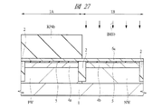
次に、図28に示されるように、フォトレジスト膜RP4aを除去してから、シリコン膜6a上に、導電体膜(導電体層)として、多結晶シリコン膜のようなシリコン膜(第2導電体層)6bを形成する。シリコン膜6bの厚み(堆積膜厚)t2は、シリコン膜6aの厚みt1よりも厚い(すなわちt2>t1)ことが好ましく、例えば80〜150nm程度とすることができる。シリコン膜6aとシリコン膜6bとの積層膜が、上記シリコン膜6に相当するものとなる。   Next, as shown in FIG. 28, after removing the photoresist film RP4a, a silicon film (second conductive film) such as a polycrystalline silicon film is formed on the silicon film 6a as a conductor film (conductor layer). Body layer) 6b is formed. The thickness (deposited film thickness) t2 of the silicon film 6b is preferably thicker than the thickness t1 of the silicon film 6a (that is, t2> t1), and can be, for example, about 80 to 150 nm. A laminated film of the silicon film 6 a and the silicon film 6 b corresponds to the silicon film 6.

次に、図29に示されるように、シリコン膜6aとシリコン膜6bとの積層膜をフォトリソグラフィ法およびドライエッチング法を用いてパターニングすることにより、ゲート電極GE1,GE2を形成する。すなわち、nMIS形成領域1Aの絶縁膜5(すなわちゲート絶縁膜5a)上にゲート電極GE1を、pMIS形成領域1Bの絶縁膜5(すなわちゲート絶縁膜5b)上にゲート電極GE2を形成する。   Next, as shown in FIG. 29, gate electrodes GE1 and GE2 are formed by patterning the laminated film of the silicon film 6a and the silicon film 6b using a photolithography method and a dry etching method. That is, the gate electrode GE1 is formed on the insulating film 5 (ie, the gate insulating film 5a) in the nMIS formation region 1A, and the gate electrode GE2 is formed on the insulating film 5 (ie, the gate insulating film 5b) in the pMIS formation region 1B.

このため、本実施の形態では、ゲート電極GE1,GE2は、シリコン膜6aとシリコン膜6a上のシリコン膜6bとの積層膜からなる。ゲート電極GE1の下に残存する絶縁膜5が、nチャネル型MISFETQnのゲート絶縁膜5aとなり、ゲート電極GE2の下に残存する絶縁膜5が、pチャネル型MISFETQpのゲート絶縁膜5bとなる。   For this reason, in the present embodiment, the gate electrodes GE1 and GE2 are formed of a laminated film of the silicon film 6a and the silicon film 6b on the silicon film 6a. The insulating film 5 remaining under the gate electrode GE1 becomes the gate insulating film 5a of the n-channel type MISFET Qn, and the insulating film 5 remaining under the gate electrode GE2 becomes the gate insulating film 5b of the p-channel type MISFET Qp.

以降の工程は、拡散防止領域10a,10b形成工程(イオン注入IM5a,IM5b)を省略すること以外は、上記実施の形態1と同様である。   Subsequent steps are the same as those in the first embodiment except that the step of forming diffusion prevention regions 10a and 10b (ion implantation IM5a and IM5b) is omitted.

すなわち、図30に示されるように、nMIS形成領域1Aの半導体基板1(p型ウエルPW)に、エクステンション領域7aおよびハロー領域8aを形成し、また、pMIS形成領域1Bの半導体基板1(n型ウエルNW)に、エクステンション領域7bおよびハロー領域8bを形成する。本実施の形態でのエクステンション領域7a,7bおよびハロー領域8a,8bの形成法と構成については、上記実施の形態1と同様である。   That is, as shown in FIG. 30, the extension region 7a and the halo region 8a are formed in the semiconductor substrate 1 (p-type well PW) in the nMIS formation region 1A, and the semiconductor substrate 1 (n-type in the pMIS formation region 1B). An extension region 7b and a halo region 8b are formed in the well NW). The formation method and configuration of the extension regions 7a and 7b and the halo regions 8a and 8b in the present embodiment are the same as those in the first embodiment.

次に、図31に示されるように、ゲート電極GE1,GE2の側壁上にサイドウォール(側壁絶縁膜)SWを形成してから、nMIS形成領域1Aの半導体基板1(p型ウエルPW)にn型半導体領域11a(ソース、ドレイン)を形成し、また、pMIS形成領域1Bの半導体基板1(n型ウエルNW)にp型半導体領域11b(ソース、ドレイン)を形成する。本実施の形態でのサイドウォールSW、n型半導体領域11aおよびp型半導体領域11bの形成法と構成については、上記実施の形態1と同様である。 Next, as shown in FIG. 31, after sidewalls (sidewall insulating films) SW are formed on the sidewalls of the gate electrodes GE1 and GE2, n are formed on the semiconductor substrate 1 (p-type well PW) in the nMIS formation region 1A. A + type semiconductor region 11a (source, drain) is formed, and a p + type semiconductor region 11b (source, drain) is formed in the semiconductor substrate 1 (n type well NW) in the pMIS formation region 1B. The formation method and configuration of the sidewall SW, the n + type semiconductor region 11a, and the p + type semiconductor region 11b in the present embodiment are the same as those in the first embodiment.

次に、上記実施の形態1と同様に、これまでのイオン注入で導入した不純物の活性化のためのアニール処理(熱処理)を行う。   Next, similarly to the first embodiment, annealing treatment (heat treatment) for activating the impurities introduced by the conventional ion implantation is performed.

その後、図32に示されるように、上記実施の形態1と同様に、ゲート電極GE1,GE2、n型半導体領域11aおよびp型半導体領域11bの表面にそれぞれ金属シリサイド層12を形成し、半導体基板1の主面上にゲート電極GE1,GE2を覆うように絶縁膜21を形成し、絶縁膜21上に絶縁膜22を形成し、絶縁膜22,21にコンタクトホール23を形成し、コンタクトホール23内にプラグ24を形成する。それから、上記実施の形態1と同様に、プラグ24が埋め込まれた絶縁膜22上に、ストッパ絶縁膜25および絶縁膜26を順に形成し、絶縁膜26およびストッパ絶縁膜25に配線溝27を形成し、配線溝27の底部および側壁上を含む絶縁膜26上にバリア導体膜28を形成し、配線溝27を銅の主導体膜29で埋め込んで配線M1を形成する。 Thereafter, as shown in FIG. 32, similarly to the first embodiment, metal silicide layers 12 are formed on the surfaces of the gate electrodes GE1, GE2, the n + type semiconductor region 11a and the p + type semiconductor region 11b, An insulating film 21 is formed on the main surface of the semiconductor substrate 1 so as to cover the gate electrodes GE1 and GE2, an insulating film 22 is formed on the insulating film 21, contact holes 23 are formed in the insulating films 22 and 21, and contacts are formed. A plug 24 is formed in the hole 23. Then, similarly to the first embodiment, a stopper insulating film 25 and an insulating film 26 are formed in order on the insulating film 22 in which the plug 24 is embedded, and a wiring groove 27 is formed in the insulating film 26 and the stopper insulating film 25. Then, a barrier conductor film 28 is formed on the insulating film 26 including the bottom and side walls of the wiring groove 27, and the wiring groove 27 is filled with a copper main conductor film 29 to form the wiring M1.

次に、本実施の形態の効果について、より詳細に説明する。   Next, the effect of this embodiment will be described in more detail.

上記実施の形態1,2では、炭素(C)、窒素(N)またはフッ素(F)のうちの1種以上が導入された拡散防止領域10a,10bまたは半導体層1bを形成することで、チャネル領域への点欠陥の拡散を防止し、それによって、チャネル領域における点欠陥の密度を抑制して、チャネルドープイオン注入でチャネル領域に導入された不純物の再配置(拡散)を抑制していた。   In the first and second embodiments, the channel is formed by forming the diffusion prevention regions 10a and 10b or the semiconductor layer 1b into which one or more of carbon (C), nitrogen (N), and fluorine (F) are introduced. The diffusion of point defects to the region is prevented, thereby suppressing the density of point defects in the channel region, and the rearrangement (diffusion) of impurities introduced into the channel region by channel doping ion implantation is suppressed.

それに対して、本実施の形態では、チャネルドープイオン注入の工程順を工夫することで、チャネルドープイオン注入でチャネル領域に導入された不純物の再配置(拡散)を抑制している。   On the other hand, in the present embodiment, the rearrangement (diffusion) of impurities introduced into the channel region by channel doping ion implantation is suppressed by devising the process order of channel doping ion implantation.

ゲート絶縁膜用の絶縁膜5を熱酸化で形成すると、熱酸化時の加熱温度が例えば700〜900℃程度と高いため、本実施の形態とは異なり、ゲート絶縁膜用の絶縁膜5形成前にチャネルドープイオン注入を行なった場合には、チャネルドープイオン注入でチャネル領域に導入された不純物が、ゲート絶縁膜用の絶縁膜5形成時の加熱(ゲート酸化時の加熱)により再配置(拡散)しやすい。   When the insulating film 5 for the gate insulating film is formed by thermal oxidation, the heating temperature at the time of the thermal oxidation is as high as about 700 to 900 ° C., for example, unlike the present embodiment, before the insulating film 5 for the gate insulating film is formed. When channel dope ion implantation is performed, impurities introduced into the channel region by channel dope ion implantation are rearranged (diffusion) by heating at the time of forming the insulating film 5 for the gate insulating film (heating at the time of gate oxidation). )It's easy to do.

そこで、本実施の形態では、ゲート絶縁膜用の絶縁膜5を形成した後で、nMIS形成領域1Aへのチャネルドープイオン注入IM1aおよびpMIS形成領域1Bへのチャネルドープイオン注入IM1bを行なってチャネルドープ層4a,4bを形成している。ゲート絶縁膜用の絶縁膜5を形成した後にチャネルドープイオン注入IM1a,IM1bを行なうことで、チャネルドープイオン注入IM1a,IM1bでチャネル領域に導入された不純物が、ゲート絶縁膜用の絶縁膜5形成時の加熱(ゲート酸化時の加熱)により再配置(拡散)することがない。すなわち、たとえゲート絶縁膜用の絶縁膜5を熱酸化で形成することで半導体基板1が高温に加熱されても、その段階ではチャネルドープイオン注入IM1a,IM1bが行なわれていないため、その後のチャネルドープイオン注入IM1a,IM1bでチャネル領域に導入された不純物が、熱酸化(ゲート酸化)時の加熱で再配置(拡散)することはない。これにより、チャネルドープイオン注入でチャネル領域に導入された不純物が、その後の加熱工程の際に再配置(拡散)されるのを抑制することができるので、MISFET毎のチャネル領域の状態(不純物分布)のばらつきを抑制して、MISFET毎のしきい値電圧のばらつきを抑制することができる。従って、半導体装置の性能を向上させることができる。   Therefore, in this embodiment, after forming the insulating film 5 for the gate insulating film, channel doping ion implantation IM1a into the nMIS formation region 1A and channel doping ion implantation IM1b into the pMIS formation region 1B are performed to perform channel doping. Layers 4a and 4b are formed. By performing channel dope ion implantation IM1a and IM1b after forming the insulating film 5 for the gate insulating film, impurities introduced into the channel region by the channel doped ion implantation IM1a and IM1b are formed in the insulating film 5 for the gate insulating film. There is no rearrangement (diffusion) due to heating during heating (heating during gate oxidation). That is, even if the semiconductor substrate 1 is heated to a high temperature by forming the insulating film 5 for the gate insulating film by thermal oxidation, the channel dope ion implantation IM1a, IM1b is not performed at that stage, so that the subsequent channel Impurities introduced into the channel region by doped ion implantation IM1a and IM1b are not rearranged (diffused) by heating during thermal oxidation (gate oxidation). As a result, it is possible to suppress the impurities introduced into the channel region by the channel doping ion implantation from being rearranged (diffused) during the subsequent heating step, so the state of the channel region (impurity distribution) for each MISFET. ) Can be suppressed, and variations in threshold voltage for each MISFET can be suppressed. Therefore, the performance of the semiconductor device can be improved.

また、本実施の形態では、ゲート絶縁膜用の絶縁膜5形成後、更にシリコン膜6aを形成した後に、nMIS形成領域1Aへのチャネルドープイオン注入IM1aおよびpMIS形成領域1Bへのチャネルドープイオン注入IM1bを行なってチャネルドープ層4a,4bを形成している。ゲート絶縁膜用の絶縁膜5がシリコン膜6aで覆われた状態(すなわち絶縁膜5が露出していない状態)でチャネルドープイオン注入IM1a,IM1bを行なうため、チャネルドープイオン注入によってゲート絶縁膜用の絶縁膜5がダメージを受けるのを防止することができる。これにより、ゲート絶縁膜5a,5bの信頼性を向上することができ、半導体装置の信頼性を向上させることができる。   In the present embodiment, after forming the insulating film 5 for the gate insulating film and further forming the silicon film 6a, channel doped ion implantation IM1a into the nMIS formation region 1A and channel doping ion implantation into the pMIS formation region 1B. IM1b is performed to form channel dope layers 4a and 4b. Channel doping ion implantation IM1a and IM1b is performed in a state where the insulating film 5 for gate insulating film is covered with the silicon film 6a (that is, the insulating film 5 is not exposed). It is possible to prevent the insulating film 5 from being damaged. Thereby, the reliability of the gate insulating films 5a and 5b can be improved, and the reliability of the semiconductor device can be improved.

また、ゲート電極の高さに相当する厚い導体膜(ゲート電極用の導体膜)を半導体基板の全面に形成した状態でチャネルドープイオン注入を行なった場合、ゲート電極用の導体膜が厚いことにより、半導体基板へのチャネルドープが的確に行えない虞がある。それに対して、本実施の形態では、シリコン膜6aが形成された状態でチャネルドープイオン注入IM1a,IM1bを行ない、その後シリコン膜6a上にシリコン膜6bを形成して、この積層膜をパターニングすることで、ゲート電極GE1,GE2を形成している。このため、ゲート電極GE1,GE2の高さよりも、シリコン膜6aの厚みt1を薄くすることができる。従って、チャネルドープイオン注入IM1a,IM1bを行なう際の、シリコン膜6aの厚みt1を薄くすることができ、半導体基板へのチャネルドープを的確に行うことができる。   In addition, when channel doping ion implantation is performed in a state where a thick conductor film (gate electrode conductor film) corresponding to the height of the gate electrode is formed on the entire surface of the semiconductor substrate, the gate electrode conductor film is thick. There is a possibility that channel doping to the semiconductor substrate cannot be performed accurately. On the other hand, in this embodiment, channel dope ion implantation IM1a and IM1b is performed in a state where the silicon film 6a is formed, and then a silicon film 6b is formed on the silicon film 6a, and this laminated film is patterned. Thus, the gate electrodes GE1 and GE2 are formed. For this reason, the thickness t1 of the silicon film 6a can be made thinner than the height of the gate electrodes GE1 and GE2. Therefore, the thickness t1 of the silicon film 6a when performing channel dope ion implantation IM1a and IM1b can be reduced, and channel doping into the semiconductor substrate can be performed accurately.

また、シリコン膜6aの厚み(堆積膜厚)t1が、シリコン膜6bの厚み(堆積膜厚)t2よりも薄いことが好ましい(すなわちt1<t2)。すなわち、ゲート電極GE1,GE2の高さは、シリコン膜6aの厚みt1とシリコン膜6bの厚みt2とを足したもの(すなわちt1+t2)に相当するが、シリコン膜6aの厚み(堆積膜厚)t1を、ゲート電極GE1,GE2の高さの半分以下にすることが好ましい。これにより、チャネルドープイオン注入IM1a,IM1bを行なう際のシリコン膜6aの厚みt1を薄くすることができるため、チャネルドープイオン注入IM1a,IM1bをより的確に行うことができる。   The thickness (deposited film thickness) t1 of the silicon film 6a is preferably smaller than the thickness (deposited film thickness) t2 of the silicon film 6b (that is, t1 <t2). That is, the height of the gate electrodes GE1 and GE2 corresponds to the sum of the thickness t1 of the silicon film 6a and the thickness t2 of the silicon film 6b (ie, t1 + t2), but the thickness (deposited film thickness) t1 of the silicon film 6a. Is preferably less than half the height of the gate electrodes GE1 and GE2. Thereby, since the thickness t1 of the silicon film 6a when performing channel dope ion implantation IM1a and IM1b can be reduced, channel dope ion implantation IM1a and IM1b can be performed more accurately.

また、本実施の形態は、ゲート絶縁膜用の絶縁膜5の形成後にチャネルドープイオン注入を行なうことで、チャネル領域の不純物に対する絶縁膜5形成時の加熱の影響を防止しているため、ゲート絶縁膜用の絶縁膜5形成時の温度が高い場合に適用すれば、効果が大きい。このため、本実施の形態は、ゲート絶縁膜用の絶縁膜5を熱酸化法で形成する場合に適用すれば、効果が極めて大きい。   Further, in the present embodiment, channel doping ion implantation is performed after the formation of the insulating film 5 for the gate insulating film, thereby preventing the influence of heating when forming the insulating film 5 on the impurities in the channel region. If applied when the temperature when forming the insulating film 5 for the insulating film is high, the effect is great. For this reason, this embodiment is very effective when applied to the case where the insulating film 5 for the gate insulating film is formed by the thermal oxidation method.

また、本実施の形態3は、上記実施の形態1,2と組み合わせることもできる。すなわち、本実施の形態3において、上記実施の形態1と同様に拡散防止領域10a,10bを形成することもでき、この場合も、拡散防止領域10a,10bの構成と形成法については、上記実施の形態1と同様である。また、本実施の形態3において、上記実施の形態2と同様の半導体基板SUB1(すなわち半導体基板1a上に半導体層1bを形成したもの)を用いることもできる。この場合、本実施の形態において、nチャネル型MISFETQnおよびpチャネル型MISFETQpのチャネル領域、p型ウエルPW、n型ウエルNW、エクステンション領域7a,7b、ハロー領域8a,8b、n型半導体領域11aおよびp型半導体領域11bは、炭素(C)、窒素(N)またはフッ素(F)のうちの1種以上が導入された半導体層1bに形成されることになる。これにより、ゲート絶縁膜用の絶縁膜5形成後にチャネルドープイオン注入を行なうことによる、チャネルドープ不純物の再配置(拡散)抑制効果と、拡散防止領域10a,10bまたは半導体層1bを設けたことでチャネル領域への点欠陥の拡散を防止したことによる、チャネルドープ不純物の再配置(拡散)抑制効果との両方を得ることができる。従って、MISFET毎のチャネル領域の状態(不純物分布)のばらつきをより的確に抑制して、MISFET毎のしきい値電圧のばらつきをより的確に抑制することができ、半導体装置の性能を更に向上させることができる。 Further, the third embodiment can be combined with the first and second embodiments. That is, in the third embodiment, the diffusion prevention regions 10a and 10b can be formed in the same manner as in the first embodiment. Also in this case, the configuration and the formation method of the diffusion prevention regions 10a and 10b are described above. This is the same as the first embodiment. In the third embodiment, the same semiconductor substrate SUB1 as in the second embodiment (that is, the semiconductor layer 1b formed on the semiconductor substrate 1a) can be used. In this case, in this embodiment, the channel region of the n-channel MISFET Qn and the p-channel MISFET Qp, the p-type well PW, the n-type well NW, the extension regions 7a and 7b, the halo regions 8a and 8b, and the n + -type semiconductor region 11a. The p + type semiconductor region 11b is formed in the semiconductor layer 1b into which one or more of carbon (C), nitrogen (N), and fluorine (F) are introduced. Thereby, the effect of suppressing the rearrangement (diffusion) of channel dope impurities by performing channel dope ion implantation after the formation of the insulating film 5 for the gate insulating film, and the provision of the diffusion prevention regions 10a and 10b or the semiconductor layer 1b. It is possible to obtain both the effect of suppressing the rearrangement (diffusion) of channel doped impurities by preventing the diffusion of point defects into the channel region. Therefore, it is possible to more accurately suppress the variation in the state (impurity distribution) of the channel region for each MISFET, to more accurately suppress the variation in the threshold voltage for each MISFET, and to further improve the performance of the semiconductor device. be able to.

(実施の形態4)
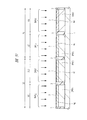
本実施の形態4の半導体装置の製造工程を図面を参照して説明する。図33〜図39は、本実施の形態の半導体装置の製造工程中の要部断面図である。
(Embodiment 4)
A manufacturing process of the semiconductor device according to the fourth embodiment will be described with reference to the drawings. 33 to 39 are main-portion cross-sectional views during the manufacturing process of the semiconductor device of the present embodiment.

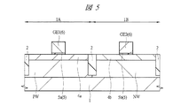
本実施の形態では、図33に示されるように、上記実施の形態1と同様に、まず、半導体基板(半導体ウエハ)1を準備し、半導体基板1の主面に素子分離領域2を形成する。   In the present embodiment, as shown in FIG. 33, as in the first embodiment, first, a semiconductor substrate (semiconductor wafer) 1 is prepared, and an element isolation region 2 is formed on the main surface of the semiconductor substrate 1. .

次に、上記実施の形態1と同様に、絶縁膜3を半導体基板1の表面に形成してから、pMIS形成領域1Bを覆うフォトレジスト膜RP1aを形成する。   Next, as in the first embodiment, after the insulating film 3 is formed on the surface of the semiconductor substrate 1, a photoresist film RP1a covering the pMIS formation region 1B is formed.

次に、nMIS形成領域1Aにおいて、半導体基板1の上層部分に、後で形成されるnチャネル型MISFETQnのしきい値調整用のイオン注入(すなわちチャネルドープイオン注入)IM1aを行なう。なお、図34では、このチャネルドープイオン注入IM1aを矢印で模式的に示してある。しきい値調整用のイオン注入IM1a、すなわちチャネルドープイオン注入IM1aでは、nチャネル型MISFETQnのチャネル領域を含む領域に、不純物(不純物イオン)が導入(イオン注入)されて、チャネルドープ層4aが形成されるため、このチャネルドープ層4aは、後でnチャネル型MISFETQnのチャネル領域となる領域を含んでいる。   Next, in the nMIS formation region 1A, ion implantation for adjusting a threshold value of an n channel MISFET Qn (that is, channel dope ion implantation) IM1a is performed on the upper layer portion of the semiconductor substrate 1 later. In FIG. 34, this channel dope ion implantation IM1a is schematically indicated by an arrow. In the ion implantation IM1a for adjusting the threshold, that is, the channel dope ion implantation IM1a, impurities (impurity ions) are introduced (ion implantation) into a region including the channel region of the n-channel MISFET Qn to form the channel dope layer 4a. Therefore, the channel dope layer 4a includes a region that later becomes the channel region of the n-channel type MISFET Qn.

本実施の形態において、このnMIS形成領域1Aへのチャネルドープイオン注入IM1aによってチャネルドープ層4aに導入される元素(不純物)は、インジウム(In)とガリウム(Ga)の一方または両方を用い、これに更にホウ素(B)を組み合わせることもできる。すなわち、本実施の形態でnMIS形成領域1Aへのチャネルドープイオン注入工程でイオン注入する元素(不純物)は、インジウム(In)か、ガリウム(Ga)か、インジウム(In)とガリウム(Ga)か、ホウ素(B)とインジウム(In)か、ホウ素(B)とガリウム(Ga)か、あるいはホウ素(B)とインジウム(In)とガリウム(Ga)である。なお、nMIS形成領域1Aへのチャネルドープイオン注入IM1aでは、pMIS形成領域1Bを覆うフォトレジスト膜RP1aは、イオン注入阻止マスクとして機能するので、pMIS形成領域1Bの半導体基板1には、イオン注入されない。   In the present embodiment, one or both of indium (In) and gallium (Ga) is used as an element (impurity) introduced into the channel dope layer 4a by the channel dope ion implantation IM1a into the nMIS formation region 1A. Further, boron (B) can be combined. That is, whether the element (impurity) to be ion-implanted in the channel doping ion implantation step into the nMIS formation region 1A in this embodiment is indium (In), gallium (Ga), indium (In), and gallium (Ga). Boron (B) and indium (In), boron (B) and gallium (Ga), or boron (B), indium (In), and gallium (Ga). Note that in the channel dope ion implantation IM1a into the nMIS formation region 1A, the photoresist film RP1a covering the pMIS formation region 1B functions as an ion implantation blocking mask, so that ions are not implanted into the semiconductor substrate 1 in the pMIS formation region 1B. .

次に、nMIS形成領域1Aにおいて、上記実施の形態1と同様にして、半導体基板1の主面から所定の深さに渡ってp型ウエルPWを形成する。本実施の形態でのp型ウエルPWの形成法と構成については、上記実施の形態1と同様である。   Next, in the nMIS formation region 1A, a p-type well PW is formed from the main surface of the semiconductor substrate 1 to a predetermined depth in the same manner as in the first embodiment. The formation method and configuration of the p-type well PW in the present embodiment are the same as those in the first embodiment.

次に、図35に示されるように、アッシングなどによりフォトレジスト膜RP1aを除去してから、上記実施の形態1と同様に、nMIS形成領域1Aを覆うフォトレジスト膜RP1bを形成する。   Next, as shown in FIG. 35, after the photoresist film RP1a is removed by ashing or the like, a photoresist film RP1b covering the nMIS formation region 1A is formed as in the first embodiment.

次に、pMIS形成領域1Bにおいて、半導体基板1の上層部分に、後で形成されるpチャネル型MISFETQpのしきい値調整用のイオン注入(すなわちチャネルドープイオン注入)IM1bを行なう。なお、図35では、このチャネルドープイオン注入IM1bを矢印で模式的に示してある。このしきい値調整用のイオン注入IM1b、すなわちチャネルドープイオン注入IM1bでは、pチャネル型MISFETQpのチャネル領域を含む領域に、不純物(不純物イオン)が導入(イオン注入)されて、チャネルドープ層4bが形成されるため、このチャネルドープ層4bは、後でpチャネル型MISFETQpのチャネル領域となる領域を含んでいる。   Next, in the pMIS formation region 1B, ion implantation for adjusting a threshold value of a p-channel type MISFET Qp to be formed later (that is, channel dope ion implantation) IM1b is performed on the upper layer portion of the semiconductor substrate 1. In FIG. 35, this channel dope ion implantation IM1b is schematically indicated by an arrow. In this threshold adjustment ion implantation IM1b, that is, channel-doped ion implantation IM1b, impurities (impurity ions) are introduced (ion-implanted) into a region including the channel region of the p-channel MISFET Qp, and the channel-doped layer 4b is formed. Since it is formed, the channel dope layer 4b includes a region that will later become a channel region of the p-channel type MISFET Qp.

本実施の形態において、このpMIS形成領域1Bへのチャネルドープイオン注入IM1bによってチャネルドープ層4bに導入される元素(不純物)は、ヒ素(As)とアンチモン(Sb)の一方または両方を用い、これに更にリン(P)を組み合わせることもできる。すなわち、本実施の形態でpMIS形成領域1Bへのチャネルドープイオン注入工程でイオン注入する元素(不純物)は、ヒ素(As)か、アンチモン(Sb)か、ヒ素(As)とアンチモン(Sb)か、リン(P)とヒ素(As)か、リン(P)とアンチモン(Sb)か、あるいはリン(P)とヒ素(As)とアンチモン(Sb)かである。なお、pMIS形成領域1Bへのチャネルドープイオン注入IM1bでは、nMIS形成領域1Aを覆うフォトレジスト膜RP1aは、イオン注入阻止マスクとして機能するので、nMIS形成領域1Aの半導体基板1には、イオン注入されない。   In the present embodiment, the element (impurity) introduced into the channel dope layer 4b by the channel dope ion implantation IM1b into the pMIS formation region 1B uses one or both of arsenic (As) and antimony (Sb). Further, phosphorus (P) can be combined. That is, whether the element (impurity) to be ion-implanted in the channel doping ion implantation step into the pMIS formation region 1B in this embodiment is arsenic (As), antimony (Sb), arsenic (As), and antimony (Sb). Phosphorus (P) and arsenic (As), phosphorus (P) and antimony (Sb), or phosphorus (P), arsenic (As) and antimony (Sb). In the channel dope ion implantation IM1b into the pMIS formation region 1B, the photoresist film RP1a covering the nMIS formation region 1A functions as an ion implantation blocking mask, so that the ion implantation is not performed on the semiconductor substrate 1 in the nMIS formation region 1A. .

次に、pMIS形成領域1Bにおいて、上記実施の形態1と同様にして、半導体基板1の主面から所定の深さに渡ってn型ウエルNWを形成する。本実施の形態でのn型ウエルNWの形成法と構成については、上記実施の形態1と同様である。   Next, in the pMIS formation region 1B, an n-type well NW is formed from the main surface of the semiconductor substrate 1 to a predetermined depth in the same manner as in the first embodiment. The formation method and configuration of the n-type well NW in the present embodiment are the same as those in the first embodiment.

以降の工程は、拡散防止領域10a,10b形成工程(イオン注入IM5a,IM5b)を省略すること以外は、上記実施の形態1と同様である。   Subsequent steps are the same as those in the first embodiment except that the step of forming diffusion prevention regions 10a and 10b (ion implantation IM5a and IM5b) is omitted.

すなわち、図36に示されるように、フォトレジスト膜RP1bを除去してから、上記絶縁膜3を除去して半導体基板1の表面を清浄化した後、nMIS形成領域1AおよびpMIS形成領域1Bの半導体基板1の表面(p型ウエルPWおよびn型ウエルNWの表面)上にゲート絶縁膜用の絶縁膜5を形成し、絶縁膜5上にゲート電極GE1,GE2を形成する。それから、図37に示されるように、nMIS形成領域1Aの半導体基板1(p型ウエルPW)に、エクステンション領域7aおよびハロー領域8aを形成し、また、pMIS形成領域1Bの半導体基板1(n型ウエルNW)に、エクステンション領域7bおよびハロー領域8bを形成する。本実施の形態での絶縁膜5、ゲート電極GE1,GE2、エクステンション領域7a,7bおよびハロー領域8a,8bの形成法と構成については、上記実施の形態1と同様である。   That is, as shown in FIG. 36, after removing the photoresist film RP1b, the insulating film 3 is removed to clean the surface of the semiconductor substrate 1, and then the semiconductors in the nMIS formation region 1A and the pMIS formation region 1B are obtained. An insulating film 5 for a gate insulating film is formed on the surface of the substrate 1 (surfaces of the p-type well PW and the n-type well NW), and gate electrodes GE1 and GE2 are formed on the insulating film 5. Then, as shown in FIG. 37, the extension region 7a and the halo region 8a are formed in the semiconductor substrate 1 (p-type well PW) in the nMIS formation region 1A, and the semiconductor substrate 1 (n-type in the pMIS formation region 1B). An extension region 7b and a halo region 8b are formed in the well NW). The formation method and configuration of the insulating film 5, the gate electrodes GE1 and GE2, the extension regions 7a and 7b, and the halo regions 8a and 8b in the present embodiment are the same as those in the first embodiment.

次に、図38に示されるように、ゲート電極GE1,GE2の側壁上にサイドウォール(側壁絶縁膜)SWを形成してから、nMIS形成領域1Aの半導体基板1(p型ウエルPW)にn型半導体領域11a(ソース、ドレイン)を形成し、また、pMIS形成領域1Bの半導体基板1(n型ウエルNW)にp型半導体領域11b(ソース、ドレイン)を形成する。本実施の形態でのサイドウォールSW、n型半導体領域11aおよびp型半導体領域11bの形成法と構成については、上記実施の形態1と同様である。 Next, as shown in FIG. 38, sidewalls (sidewall insulating films) SW are formed on the sidewalls of the gate electrodes GE1 and GE2, and then n is formed on the semiconductor substrate 1 (p-type well PW) in the nMIS formation region 1A. A + type semiconductor region 11a (source, drain) is formed, and a p + type semiconductor region 11b (source, drain) is formed in the semiconductor substrate 1 (n type well NW) in the pMIS formation region 1B. The formation method and configuration of the sidewall SW, the n + type semiconductor region 11a, and the p + type semiconductor region 11b in the present embodiment are the same as those in the first embodiment.

次に、上記実施の形態1と同様に、これまでのイオン注入で導入した不純物の活性化のためのアニール処理(熱処理)を行う。   Next, similarly to the first embodiment, annealing treatment (heat treatment) for activating the impurities introduced by the conventional ion implantation is performed.

その後、図39に示されるように、上記実施の形態1と同様に、ゲート電極GE1,GE2、n型半導体領域11aおよびp型半導体領域11bの表面にそれぞれ金属シリサイド層12を形成し、半導体基板1の主面上にゲート電極GE1,GE2を覆うように絶縁膜21を形成し、絶縁膜21上に絶縁膜22を形成し、絶縁膜22,21にコンタクトホール23を形成し、コンタクトホール23内にプラグ24を形成する。それから、上記実施の形態1と同様に、プラグ24が埋め込まれた絶縁膜22上に、ストッパ絶縁膜25および絶縁膜26を順に形成し、絶縁膜26およびストッパ絶縁膜25に配線溝27を形成し、配線溝27の底部および側壁上を含む絶縁膜26上にバリア導体膜28を形成し、配線溝27を銅の主導体膜29で埋め込んで配線M1を形成する。 Thereafter, as shown in FIG. 39, similarly to the first embodiment, metal silicide layers 12 are formed on the surfaces of the gate electrodes GE1, GE2, the n + type semiconductor region 11a and the p + type semiconductor region 11b, An insulating film 21 is formed on the main surface of the semiconductor substrate 1 so as to cover the gate electrodes GE1 and GE2, an insulating film 22 is formed on the insulating film 21, contact holes 23 are formed in the insulating films 22 and 21, and contacts are formed. A plug 24 is formed in the hole 23. Then, similarly to the first embodiment, a stopper insulating film 25 and an insulating film 26 are formed in order on the insulating film 22 in which the plug 24 is embedded, and a wiring groove 27 is formed in the insulating film 26 and the stopper insulating film 25. Then, a barrier conductor film 28 is formed on the insulating film 26 including the bottom and side walls of the wiring groove 27, and the wiring groove 27 is filled with a copper main conductor film 29 to form the wiring M1.

次に、本実施の形態の効果について、より詳細に説明する。   Next, the effect of this embodiment will be described in more detail.

上記実施の形態1〜3では、チャネルドープイオン注入IM1a,IM1bで導入された不純物が、イオン注入後に拡散されにくいように工夫していた。それに対して、本実施の形態では、チャネルドープイオン注入後に拡散されにくいような元素(不純物)を、チャネルドープイオン注入IM1a,IM1bで注入している。   In the first to third embodiments, the impurities introduced by the channel dope ion implantation IM1a and IM1b are devised so that they are not easily diffused after the ion implantation. In contrast, in the present embodiment, elements (impurities) that are difficult to diffuse after channel doping ion implantation are implanted by channel doping ion implantation IM1a and IM1b.

すなわち、イオン注入された元素(不純物)は、原子番号が大きい元素ほど(すなわち重い元素ほど)、イオン注入後の加熱によって移動(拡散)しにくく、イオン打ち込みで配置された位置に留まりやすい。このため、原子番号が小さな軽い不純物元素をイオン注入した場合、注入直後の段階では、注入された不純物元素はランダムに配置されていても、その後の種々の加熱工程で不純物元素が拡散(移動)して、不純物元素の配置のランダム性が低下しやすいのに比べて、原子番号が大きな重い不純物元素をイオン注入した場合、注入直後の不純物元素のランダムな配置は、その後の種々の加熱工程を経ても維持されやすい。   That is, an ion-implanted element (impurity) is more difficult to move (diffusion) by heating after ion implantation as the element with a larger atomic number (that is, heavier element) and stays at the position where ion implantation is performed. For this reason, when a light impurity element having a small atomic number is ion-implanted, the impurity element diffuses (moves) in various subsequent heating steps even if the implanted impurity element is randomly arranged in the stage immediately after the implantation. When the impurity element having a large atomic number is ion-implanted compared to the random arrangement of the impurity element, the random arrangement of the impurity element immediately after the implantation is performed in various subsequent heating steps. It is easy to maintain even after passing.

そこで、本実施の形態では、チャネルドープイオン注入IM1a,IM1bに、原子番号が大きい元素(すなわち重い元素)を用いる。   Therefore, in this embodiment, an element having a large atomic number (that is, a heavy element) is used for channel dope ion implantation IM1a and IM1b.

nMIS形成領域1A(nチャネル型MISFETQn)について具体的に説明すると、nMIS形成領域1Aへのチャネルドープイオン注入IM1aに用いる元素(すなわちチャネルドープイオン注入IM1aでチャネルドープ層4aに導入される不純物元素)として、インジウム(In)とガリウム(Ga)の一方または両方を用いる。インジウム(In)およびガリウム(Ga)は、ホウ素(B)と同様にp型の不純物として機能できるが、ホウ素(B)よりも原子番号が大きく重いため、ホウ素(B)に比べて、注入後の加熱によって移動(拡散)されにくい。このため、チャネルドープイオン注入IM1aでチャネルドープ層4aに導入された不純物(ここではインジウム(In)とガリウム(Ga)の一方または両方)は、注入直後の不純物元素のランダムな配置が、その後の種々の加熱工程を経ても維持されやすい。これにより、チャネルドープイオン注入IM1aでnチャネル型MISFETQnのチャネル領域(チャネルドープ層4a)に導入された不純物(ここではインジウム(In)とガリウム(Ga)の一方または両方)が、その後の加熱工程の際に再配置(拡散)されるのを抑制または防止することができるので、nチャネル型MISFET毎のチャネル領域の状態(不純物分布)のばらつきを抑制することができる。従って、nチャネル型MISFET毎のしきい値電圧のばらつきを抑制することができ、半導体装置の性能を向上させることができる。   The nMIS formation region 1A (n-channel type MISFET Qn) will be described in detail. Elements used for the channel dope ion implantation IM1a into the nMIS formation region 1A (that is, impurity elements introduced into the channel dope layer 4a by the channel dope ion implantation IM1a) One or both of indium (In) and gallium (Ga) is used. Indium (In) and gallium (Ga) can function as p-type impurities like boron (B), but have a larger atomic number than boron (B) and are therefore heavier than boron (B). It is difficult to move (diffuse) by heating. For this reason, the impurity introduced into the channel dope layer 4a by the channel dope ion implantation IM1a (here, one or both of indium (In) and gallium (Ga)) is a random arrangement of the impurity element immediately after the implantation. It is easy to maintain even through various heating processes. Thereby, impurities (here, one or both of indium (In) and gallium (Ga)) introduced into the channel region (channel dope layer 4a) of the n-channel type MISFET Qn by the channel dope ion implantation IM1a are subjected to a subsequent heating step. In this case, rearrangement (diffusion) can be suppressed or prevented, so that variation in the state (impurity distribution) of the channel region for each n-channel MISFET can be suppressed. Therefore, variations in threshold voltage for each n-channel MISFET can be suppressed, and the performance of the semiconductor device can be improved.

また、nMIS形成領域1Aへのチャネルドープイオン注入IM1aに用いる元素(すなわちチャネルドープイオン注入IM1aでチャネルドープ層4aに導入される不純物元素)としては、インジウム(In)とガリウム(Ga)の一方または両方を用いることがより好ましいが、これに更にホウ素(B)を組み合わせることもできる。この場合、注入したホウ素(B)は、注入後の加熱により拡散(移動)してランダム配置が崩れても、注入したインジウム(In)とガリウム(Ga)の一方または両方は、注入後の加熱を経てもランダム配置を維持しやすいため、チャネルドープイオン注入にホウ素(B)のみを用いた場合に比べて、nチャネル型MISFET毎のチャネル領域の状態(不純物分布)のばらつきを抑制することができる。このため、チャネルドープイオン注入にホウ素(B)のみを用いた場合に比べて、nチャネル型MISFET毎のしきい値電圧のばらつきを抑制することができる。   Further, as an element used for the channel dope ion implantation IM1a to the nMIS formation region 1A (that is, an impurity element introduced into the channel dope layer 4a by the channel dope ion implantation IM1a), one of indium (In) and gallium (Ga) or Although it is more preferable to use both, boron (B) can be further combined with this. In this case, even if the implanted boron (B) is diffused (moved) by the heating after the implantation and the random arrangement is destroyed, one or both of the implanted indium (In) and gallium (Ga) is heated after the implantation. Since it is easy to maintain a random arrangement even after passing through, it is possible to suppress variations in the state (impurity distribution) of the channel region for each n-channel type MISFET as compared with the case where only boron (B) is used for channel doping ion implantation. it can. For this reason, it is possible to suppress variations in threshold voltage for each n-channel type MISFET as compared with the case where only boron (B) is used for channel doping ion implantation.

また、pMIS形成領域1B(pチャネル型MISFETQp)について具体的に説明すると、pMIS形成領域1Bへのチャネルドープイオン注入IM1bに用いる元素(すなわちチャネルドープイオン注入IM1bでチャネルドープ層4bに導入される不純物元素)として、ヒ素(As)とアンチモン(Sb)の一方または両方を用いる。ヒ素(As)およびアンチモン(Sb)は、リン(P)と同様にn型の不純物として機能できるが、リン(P)よりも原子番号が大きく重いため、リン(P)に比べて、注入後の加熱によって移動(拡散)されにくい。このため、チャネルドープイオン注入IM1bでチャネルドープ層4bに導入された不純物(ここではヒ素(As)とアンチモン(Sb)の一方または両方)は、注入直後の不純物元素のランダムな配置が、その後の種々の加熱工程を経ても維持されやすい。これにより、チャネルドープイオン注入IM1bでpチャネル型MISFETQpのチャネル領域(チャネルドープ層4b)に導入された不純物(ここではヒ素(As)とアンチモン(Sb)の一方または両方)が、その後の加熱工程の際に再配置(拡散)されるのを抑制または防止することができるので、pチャネル型MISFET毎のチャネル領域の状態(不純物分布)のばらつきを抑制することができる。従って、pチャネル型MISFET毎のしきい値電圧のばらつきを抑制することができ、半導体装置の性能を向上させることができる。   The pMIS formation region 1B (p channel type MISFET Qp) will be described in detail. Elements used for the channel dope ion implantation IM1b into the pMIS formation region 1B (that is, impurities introduced into the channel dope layer 4b by the channel dope ion implantation IM1b). As the element, one or both of arsenic (As) and antimony (Sb) is used. Arsenic (As) and antimony (Sb) can function as n-type impurities like phosphorus (P), but have a larger atomic number than phosphorus (P) and are therefore heavier than phosphorus (P). It is difficult to move (diffuse) by heating. For this reason, the impurity introduced into the channel dope layer 4b by the channel dope ion implantation IM1b (here, one or both of arsenic (As) and antimony (Sb)) is a random arrangement of the impurity element immediately after the implantation. It is easy to maintain even through various heating processes. Thereby, impurities (here, one or both of arsenic (As) and antimony (Sb)) introduced into the channel region (channel doped layer 4b) of the p-channel type MISFET Qp by the channel-doped ion implantation IM1b are heated in the subsequent heating step. In this case, rearrangement (diffusion) can be suppressed or prevented, so that variation in the state (impurity distribution) of the channel region for each p-channel MISFET can be suppressed. Therefore, variation in threshold voltage for each p-channel MISFET can be suppressed, and the performance of the semiconductor device can be improved.

また、pMIS形成領域1Bへのチャネルドープイオン注入IM1bに用いる元素(すなわちチャネルドープイオン注入IM1bでチャネルドープ層4bに導入される不純物元素)としては、ヒ素(As)とアンチモン(Sb)の一方または両方を用いることがより好ましいが、これに更にリン(P)を組み合わせることもできる。この場合、注入したリン(P)は、注入後の加熱により拡散(移動)してランダム配置が崩れても、注入したヒ素(As)とアンチモン(Sb)の一方または両方は、注入後の加熱を経てもランダム配置を維持しやすいため、チャネルドープイオン注入にリン(P)のみを用いた場合に比べて、pチャネル型MISFET毎のチャネル領域の状態(不純物分布)のばらつきを抑制することができる。このため、チャネルドープイオン注入にリン(P)のみを用いた場合に比べて、pチャネル型MISFET毎のしきい値電圧のばらつきを抑制することができる。   In addition, as an element used for channel dope ion implantation IM1b into pMIS formation region 1B (that is, an impurity element introduced into channel dope layer 4b by channel dope ion implantation IM1b), one of arsenic (As) and antimony (Sb) or Although it is more preferable to use both, phosphorus (P) can also be combined with this. In this case, even if the injected phosphorus (P) is diffused (moved) by the heating after the injection and the random arrangement is destroyed, one or both of the injected arsenic (As) and antimony (Sb) are heated after the injection. Since it is easy to maintain a random arrangement even after passing through, it is possible to suppress variations in the state (impurity distribution) of the channel region for each p-channel type MISFET as compared with the case where only phosphorus (P) is used for channel doping ion implantation. it can. For this reason, it is possible to suppress variation in threshold voltage for each p-channel type MISFET as compared with the case where only phosphorus (P) is used for channel dope ion implantation.

上記実施の形態1,2,3のそれぞれにおいて、あるいはそれらを組み合わせたものにおいても、チャネルドープイオン注入IM1a,IM1bに用いる不純物元素の種類を、本実施の形態4と同様とすることもできる。   In each of the first, second, and third embodiments, or a combination thereof, the types of impurity elements used for channel dope ion implantation IM1a and IM1b can be the same as those in the fourth embodiment.

例えば、上記実施の形態1において、nMIS形成領域1Aへのチャネルドープイオン注入IM1aに、インジウム(In)とガリウム(Ga)の一方または両方か、あるいはこれに更にホウ素(B)を組み合わせたものを用い、pMIS形成領域1Bへのチャネルドープイオン注入IM1bに、ヒ素(As)とアンチモン(Sb)の一方または両方か、あるいはこれに更にリン(P)を組み合わせたものを用いることができる。これにより、本実施の形態4と同様の不純物元素をチャネルドープイオン注入IM1a,IM1bで注入したことにより、注入された不純物元素自身が、注入後の加熱により移動(拡散)しにくくなり、更に上記実施の形態1のように拡散防止領域10a,10bを形成したことにより、チャネル領域における点欠陥の密度を抑制してチャネル領域で不純物元素が点欠陥を介して移動(拡散)しにくくすることができる。   For example, in the first embodiment, one or both of indium (In) and gallium (Ga), or a combination of boron (B) with the channel doped ion implantation IM1a into the nMIS formation region 1A is used. In addition, one or both of arsenic (As) and antimony (Sb), or a combination of phosphorus and phosphorus (P) can be used for the channel dope ion implantation IM1b into the pMIS formation region 1B. As a result, the same impurity element as in the fourth embodiment is implanted by the channel dope ion implantation IM1a and IM1b, so that the implanted impurity element itself is less likely to move (diffusion) by the heating after the implantation. By forming the diffusion prevention regions 10a and 10b as in the first embodiment, the density of point defects in the channel region is suppressed, and the impurity element is less likely to move (diffuse) through the point defects in the channel region. it can.

また、上記実施の形態2において、nMIS形成領域1Aへのチャネルドープイオン注入IM1aに、インジウム(In)とガリウム(Ga)の一方または両方か、あるいはこれに更にホウ素(B)を組み合わせたものを用い、pMIS形成領域1Bへのチャネルドープイオン注入IM1bに、ヒ素(As)とアンチモン(Sb)の一方または両方か、あるいはこれに更にリン(P)を組み合わせたものを用いることができる。これにより、本実施の形態4と同様の不純物元素をチャネルドープイオン注入で注入したことにより、注入された不純物元素自身が、注入後の加熱により移動(拡散)しにくくなる。更に上記実施の形態2のように炭素(C)、窒素(N)またはフッ素(F)のうちの1種以上が導入された半導体層1bにnチャネル型MISFETQnおよびpチャネル型MISFETQpを形成したことにより、チャネル領域における点欠陥の密度を抑制してチャネル領域で不純物元素が点欠陥を介して移動(拡散)しにくくすることができる。   In the second embodiment, the channel dope ion implantation IM1a into the nMIS formation region 1A includes one or both of indium (In) and gallium (Ga), or a combination of boron and (B). In addition, one or both of arsenic (As) and antimony (Sb), or a combination of phosphorus and phosphorus (P) can be used for the channel dope ion implantation IM1b into the pMIS formation region 1B. As a result, the same impurity element as in the fourth embodiment is implanted by channel dope ion implantation, so that the implanted impurity element itself is less likely to move (diffusion) by heating after implantation. Further, the n-channel MISFET Qn and the p-channel MISFET Qp are formed in the semiconductor layer 1b into which one or more of carbon (C), nitrogen (N), or fluorine (F) is introduced as in the second embodiment. Accordingly, it is possible to suppress the density of point defects in the channel region and to make it difficult for the impurity element to move (diffuse) through the point defect in the channel region.

また、上記実施の形態3において、nMIS形成領域1Aへのチャネルドープイオン注入IM1aに、インジウム(In)とガリウム(Ga)の一方または両方か、あるいはこれに更にホウ素(B)を組み合わせたものを用い、pMIS形成領域1Bへのチャネルドープイオン注入IM1bに、ヒ素(As)とアンチモン(Sb)の一方または両方か、あるいはこれに更にリン(P)を組み合わせたものを用いることができる。これにより、本実施の形態4と同様の不純物元素をチャネルドープイオン注入で注入したことにより、注入された不純物元素自身が、注入後の加熱により移動(拡散)しにくくなり、更に上記実施の形態3のように、ゲート絶縁膜用の絶縁膜5を形成した後にチャネルドープイオン注入を行なうことで、チャネルドープイオン注入後の加熱工程(ゲート酸化工程)を削減できる。   Further, in the third embodiment, one or both of indium (In) and gallium (Ga), or a combination of boron (B) with the channel dope ion implantation IM1a into the nMIS formation region 1A is used. In addition, one or both of arsenic (As) and antimony (Sb), or a combination of phosphorus and phosphorus (P) can be used for the channel dope ion implantation IM1b into the pMIS formation region 1B. As a result, the same impurity element as in the fourth embodiment is implanted by channel dope ion implantation, so that the implanted impurity element itself is less likely to move (diffusion) by the heating after the implantation, and further the above-described embodiment. As shown in FIG. 3, the channel doping ion implantation is performed after the insulating film 5 for the gate insulating film is formed, so that the heating process (gate oxidation process) after the channel doping ion implantation can be reduced.

また、例えば、上記実施の形態1と上記実施の形態3とを組み合わせたものにおいて、チャネルドープイオン注入IM1a,IM1bに用いる不純物元素の種類を、本実施の形態4と同様とすることもでき、また、上記実施の形態2と上記実施の形態3とを組み合わせたものにおいて、チャネルドープイオン注入IM1a,IM1bに用いる不純物元素の種類を、本実施の形態4と同様とすることもできる。   Further, for example, in the combination of the first embodiment and the third embodiment, the types of impurity elements used for the channel dope ion implantation IM1a and IM1b can be the same as those in the fourth embodiment. Further, in the combination of the second embodiment and the third embodiment, the types of impurity elements used for the channel dope ion implantation IM1a and IM1b can be the same as those in the fourth embodiment.

このように、上記実施の形態1,2,3のそれぞれにおいて、あるいはそれらを組み合わせたものにおいて、チャネルドープイオン注入IM1a,IM1bに用いる不純物元素の種類を、本実施の形態4と同様とすることで、チャネルドープイオン注入でチャネル領域に導入された不純物の、注入直後のランダム配置を、注入後も更に的確に維持することができる。このため、MISFET毎のチャネル領域の状態(不純物分布)のばらつきをより的確に抑制して、MISFET毎のしきい値電圧のばらつきをより的確に抑制することができ、半導体装置の性能をより的確に向上させることができる。   As described above, in each of the first, second, and third embodiments, or a combination thereof, the types of impurity elements used for the channel dope ion implantation IM1a and IM1b are the same as those in the fourth embodiment. Thus, the random arrangement immediately after the implantation of the impurities introduced into the channel region by the channel dope ion implantation can be maintained more accurately after the implantation. For this reason, it is possible to more accurately suppress the variation in the state (impurity distribution) of the channel region for each MISFET, to more accurately suppress the variation in the threshold voltage for each MISFET, and to improve the performance of the semiconductor device more accurately. Can be improved.

(実施の形態5)
図40は、上記実施の形態1〜4またはそれらを組み合わせた製造工程により製造された半導体装置(半導体チップ)SM1の一例を示す平面図である。
(Embodiment 5)
FIG. 40 is a plan view showing an example of the semiconductor device (semiconductor chip) SM1 manufactured through the manufacturing steps according to the first to fourth embodiments or a combination thereof.

本実施の形態の半導体装置SM1は、SRAM(Static Random Access Memory)などのメモリセルアレイが形成されたメモリ領域(メモリ回路領域、メモリセルアレイ領域、SRAM領域)31と、メモリ以外の回路(周辺回路)が形成された周辺回路領域32とを有している。周辺回路領域32は、例えば、アナログ回路が形成されたアナログ回路領域や、制御回路が形成されたCPU領域などを含んでいる。メモリ領域31と周辺回路領域32との間や、周辺回路領域32同士の間は、半導体装置SM1の内部配線層を介して必要に応じて電気的に接続されている。また、半導体装置SM1の主面(表面)の周辺部には、半導体装置SM1の主面の四辺に沿って複数のパッド電極PDが形成されている。各パッド電極PDは、半導体装置SM1の内部配線層を介してメモリ領域31や周辺回路領域32などに電気的に接続されている。   The semiconductor device SM1 of the present embodiment includes a memory region (memory circuit region, memory cell array region, SRAM region) 31 in which a memory cell array such as SRAM (Static Random Access Memory) is formed, and a circuit (peripheral circuit) other than the memory. And a peripheral circuit region 32 in which is formed. The peripheral circuit area 32 includes, for example, an analog circuit area in which an analog circuit is formed, a CPU area in which a control circuit is formed, and the like. The memory region 31 and the peripheral circuit region 32 or between the peripheral circuit regions 32 are electrically connected as necessary via an internal wiring layer of the semiconductor device SM1. In addition, a plurality of pad electrodes PD are formed along the four sides of the main surface of the semiconductor device SM1 at the periphery of the main surface (front surface) of the semiconductor device SM1. Each pad electrode PD is electrically connected to the memory region 31 and the peripheral circuit region 32 through the internal wiring layer of the semiconductor device SM1.

本実施の形態では、半導体装置SM1を製造するにあたって、上記実施の形態1〜4の製造技術のいずれか、またはその組み合わせを用いることができる。ここで、上記実施の形態1の製造技術とは、上記拡散防止領域10a,10bを設けることに対応する。上記実施の形態2の製造技術とは、上記半導体層1bを設けてそこにMISFETを形成することに対応する。上記実施の形態3の製造技術とは、ゲート絶縁膜用の上記絶縁膜5および上記シリコン膜6aの形成後に上記チャネルドープイオン注入IM1a,IM1bを行なってからシリコン膜6a上に上記シリコン膜6bを形成し、この積層膜(シリコン膜6a,6b)をパターニングしてゲート電極を形成することに対応する。上記実施の形態4の製造技術とは、チャネルドープイオン注入IM1a,IM1bで注入する元素の種類を上記実施の形態4のように選択することに対応する。   In the present embodiment, when manufacturing the semiconductor device SM1, any one of the manufacturing techniques of the first to fourth embodiments or a combination thereof can be used. Here, the manufacturing technique of the first embodiment corresponds to providing the diffusion prevention regions 10a and 10b. The manufacturing technique of the second embodiment corresponds to providing the semiconductor layer 1b and forming a MISFET there. The manufacturing technique of the third embodiment is that the channel doped ion implantation IM1a, IM1b is performed after the formation of the insulating film 5 for the gate insulating film and the silicon film 6a, and then the silicon film 6b is formed on the silicon film 6a. This corresponds to forming a gate electrode by patterning the laminated film (silicon films 6a and 6b). The manufacturing technique of the fourth embodiment corresponds to selecting the type of element to be implanted by channel dope ion implantation IM1a and IM1b as in the fourth embodiment.

半導体装置SM1を製造するにあたって、上記実施の形態3の製造技術を適用する場合は、半導体装置SM1(半導体基板1)における全ての領域(メモリ領域31および周辺回路領域32の全て)のMISFETに対して適用することが好ましく、これにより、半導体装置の製造工程を簡略化できる。   In manufacturing the semiconductor device SM1, when the manufacturing technique of the third embodiment is applied, the MISFETs in all regions (the memory region 31 and the peripheral circuit region 32) in the semiconductor device SM1 (semiconductor substrate 1) are applied. The semiconductor device manufacturing process can be simplified.

一方、半導体装置SM1を製造するにあたって、上記実施の形態1,2,4の製造技術(単独又は組合せ)を適用する場合は、半導体装置SM1における全ての領域(メモリ領域31および周辺回路領域32の全て)に対して適用するのではなく、メモリ領域31について適用するが、周辺回路領域32については、適用する周辺回路領域32aと適用しない周辺回路領域32bとを混在させる。適用しない周辺回路領域32bは、例えば、上記アナログ回路領域やCPU領域である。なお、図40は平面図であるが、理解を簡単にするために、上記実施の形態1,2,4の製造技術(単独又は組合せ)を適用するメモリ領域31および周辺回路領域32aにハッチングを付してある。   On the other hand, in manufacturing the semiconductor device SM1, when the manufacturing techniques (single or combined) of the first, second, and fourth embodiments are applied, all the regions (the memory region 31 and the peripheral circuit region 32 of the semiconductor device SM1) are applied. However, the peripheral circuit area 32 is mixed with the peripheral circuit area 32a to be applied and the peripheral circuit area 32b not to be applied. The peripheral circuit area 32b that is not applied is, for example, the analog circuit area or the CPU area. 40 is a plan view, but in order to facilitate understanding, hatching is applied to the memory region 31 and the peripheral circuit region 32a to which the manufacturing techniques (single or combined) of the first, second, and fourth embodiments are applied. It is attached.

まず、半導体装置SM1を製造するにあたって、上記実施の形態1の製造技術を適用する場合について説明する。この場合、メモリ領域31と周辺回路領域32aにおいては、nチャネル型MISFETおよびpチャネル型MISFETを形成する際に、上記拡散防止領域10a,10bに対応するものを形成する。それに対して、周辺回路領域32bにおいては、nチャネル型MISFETおよびpチャネル型MISFETを形成する際に、上記拡散防止領域10a,10bに対応するものを形成しない。   First, the case where the manufacturing technique of the first embodiment is applied in manufacturing the semiconductor device SM1 will be described. In this case, in the memory region 31 and the peripheral circuit region 32a, those corresponding to the diffusion preventing regions 10a and 10b are formed when the n-channel MISFET and the p-channel MISFET are formed. On the other hand, in the peripheral circuit region 32b, when the n-channel MISFET and the p-channel MISFET are formed, those corresponding to the diffusion preventing regions 10a and 10b are not formed.

次に、半導体装置SM1を製造するにあたって、上記実施の形態2の製造技術を適用する場合について説明する。この場合、メモリ領域31と周辺回路領域32aにおいては、上記半導体層1bに相当する領域(炭素、窒素またはフッ素のうちの1種以上が導入された半導体層)をイオン注入で形成しておき、そこにnチャネル型MISFETおよびpチャネル型MISFETを形成する。それに対して、周辺回路領域32bにおいては、上記半導体層1bに相当する領域を形成せずに、基板領域(炭素、窒素またはフッ素が導入されていない半導体基板領域)にnチャネル型MISFETおよびpチャネル型MISFETを形成する。   Next, a case where the manufacturing technique of the second embodiment is applied when manufacturing the semiconductor device SM1 will be described. In this case, in the memory region 31 and the peripheral circuit region 32a, a region corresponding to the semiconductor layer 1b (a semiconductor layer into which one or more of carbon, nitrogen, and fluorine are introduced) is formed by ion implantation. An n-channel MISFET and a p-channel MISFET are formed there. On the other hand, in the peripheral circuit region 32b, the region corresponding to the semiconductor layer 1b is not formed, and the n-channel MISFET and the p-channel are formed in the substrate region (semiconductor substrate region into which carbon, nitrogen, or fluorine is not introduced). A type MISFET is formed.

次に、半導体装置SM1を製造するにあたって、上記実施の形態4の製造技術を適用する場合について説明する。この場合、メモリ領域31と周辺回路領域32aにおいては、nチャネル型MISFETのチャネルドープイオン注入には、上記実施の形態4においてnMIS形成領域1Aに対して行ったチャネルドープイオン注入IM1aと同種の元素を用い、pチャネル型MISFETのチャネルドープイオン注入には、上記実施の形態4においてpMIS形成領域1Bに対して行ったチャネルドープイオン注入IM1bと同種の元素を用いる。それに対して、周辺回路領域32aにおいては、nチャネル型MISFETのチャネルドープイオン注入には、ホウ素(B)のみを用い、pチャネル型MISFETのチャネルドープイオン注入には、リン(P)のみを用いる。   Next, a case where the manufacturing technique of the fourth embodiment is applied when manufacturing the semiconductor device SM1 will be described. In this case, in the memory region 31 and the peripheral circuit region 32a, the same kind of element as the channel dope ion implantation IM1a performed for the nMIS formation region 1A in the fourth embodiment is used for the channel dope ion implantation of the n channel MISFET. In the channel dope ion implantation of the p-channel type MISFET, the same element as the channel dope ion implantation IM1b performed for the pMIS formation region 1B in the fourth embodiment is used. On the other hand, in the peripheral circuit region 32a, only boron (B) is used for channel doping ion implantation of the n-channel MISFET, and only phosphorus (P) is used for channel doping ion implantation of the p-channel MISFET. .

一例として、上記実施の形態1の製造技術と上記実施の形態4の製造技術とを適用して半導体装置SM1を製造する場合について、以下で図41〜図47を参照して具体的に説明する。この場合、メモリ領域31と周辺回路領域32aについては、上記実施の形態1の製造技術と上記実施の形態4の製造技術とを適用するが、周辺回路領域32bについては、上記実施の形態1の製造技術と上記実施の形態4の製造技術とを適用しない。   As an example, a case where the semiconductor device SM1 is manufactured by applying the manufacturing technique of the first embodiment and the manufacturing technique of the fourth embodiment will be specifically described below with reference to FIGS. . In this case, the manufacturing technique of the first embodiment and the manufacturing technique of the fourth embodiment are applied to the memory area 31 and the peripheral circuit area 32a, but the peripheral circuit area 32b is the same as that of the first embodiment. The manufacturing technique and the manufacturing technique of the fourth embodiment are not applied.

図41〜図47は、本実施の形態の半導体装置SM1の製造工程中の要部断面図であり、上記実施の形態1と上記実施の形態4を適用して半導体装置SM1を製造する場合の要部断面図が示されている。   41 to 47 are principal part cross-sectional views during the manufacturing process of the semiconductor device SM1 of the present embodiment, in the case of manufacturing the semiconductor device SM1 by applying the first embodiment and the fourth embodiment. A cross-sectional view of the main part is shown.

本実施の形態では、上記実施の形態1と同様に、まず、半導体基板(半導体ウエハ)1を準備する。図41には、半導体基板1のうち、メモリ領域31の一部と周辺回路領域32aの一部と周辺回路領域32bの一部とが示されている。   In the present embodiment, as in the first embodiment, first, a semiconductor substrate (semiconductor wafer) 1 is prepared. FIG. 41 shows a part of the memory region 31, a part of the peripheral circuit region 32a, and a part of the peripheral circuit region 32b in the semiconductor substrate 1.

メモリ領域31のうち、図41には、メモリ(メモリセル)を構成するnチャネル型MISFETが形成される領域であるメモリnMIS形成領域1Cと、メモリ(メモリセル)を構成するpチャネル型MISFETが形成される領域であるメモリpMIS形成領域1Dとが示されている。   Among the memory regions 31, FIG. 41 shows a memory nMIS formation region 1C, which is a region where an n-channel MISFET constituting the memory (memory cell) is formed, and a p-channel MISFET constituting the memory (memory cell). A memory pMIS formation region 1D, which is a region to be formed, is shown.

また、周辺回路領域32には、耐圧が異なるMISFETが形成される。このため、図41には、周辺回路領域32aにおいて低耐圧のnチャネル型MISFETが形成される領域である低耐圧nMIS形成領域1L1が示されている。また、図41には、周辺回路領域32bにおいて低耐圧のnチャネル型MISFETが形成される領域である低耐圧nMIS形成領域1L2と高耐圧のnチャネル型MISFETが形成される領域である高耐圧nMIS形成領域1Hとが示されている。   In the peripheral circuit region 32, MISFETs having different breakdown voltages are formed. Therefore, FIG. 41 shows a low breakdown voltage nMIS formation region 1L1, which is a region where a low breakdown voltage n-channel MISFET is formed in the peripheral circuit region 32a. Also, FIG. 41 shows a low breakdown voltage nMIS formation region 1L2, which is a region where a low breakdown voltage n-channel MISFET is formed in the peripheral circuit region 32b, and a high breakdown voltage nMIS, which is a region where a high breakdown voltage n-channel MISFET is formed. A formation region 1H is shown.

半導体装置SM1を製造するには、図41に示されるように、まず、上記実施の形態1と同様に半導体基板(半導体ウエハ)1を準備する。それから、半導体基板1の主面に素子分離領域2を形成する。   In order to manufacture the semiconductor device SM1, as shown in FIG. 41, first, a semiconductor substrate (semiconductor wafer) 1 is prepared as in the first embodiment. Then, the element isolation region 2 is formed on the main surface of the semiconductor substrate 1.

次に、上記実施の形態1と同様の絶縁膜3を半導体基板1の表面に形成してから、図42に示されるように、メモリnMIS形成領域1Cにp型ウエルPW1を、メモリpMIS形成領域1Dにn型ウエルNW1を、低耐圧nMIS形成領域1L1にp型ウエルPW2を、低耐圧nMIS形成領域1L2にp型ウエルPW3を、高耐圧nMIS形成領域1Hにp型ウエルPW4を、それぞれ形成する。p型ウエルPW1,PW2,PW3,PW4およびn型ウエルNW1は、それぞれフォトレジスト膜(図示せず)をイオン注入阻止マスクとして用いたイオン注入によって形成することができる。p型ウエルPW1を形成するためのイオン注入とp型ウエルPW2を形成するためのイオン注入とp型ウエルPW3を形成するためのイオン注入とp型ウエルPW4を形成するためのイオン注入とは、同じイオン注入工程で行なえば工程数を低減できるが、異なるイオン注入工程として行なってもよい。   Next, after the insulating film 3 similar to that of the first embodiment is formed on the surface of the semiconductor substrate 1, as shown in FIG. 42, the p-type well PW1 is formed in the memory nMIS formation region 1C, and the memory pMIS formation region. An n-type well NW1 is formed in 1D, a p-type well PW2 is formed in the low breakdown voltage nMIS formation region 1L1, a p-type well PW3 is formed in the low breakdown voltage nMIS formation region 1L2, and a p-type well PW4 is formed in the high breakdown voltage nMIS formation region 1H. . The p-type wells PW1, PW2, PW3, PW4 and the n-type well NW1 can be formed by ion implantation using a photoresist film (not shown) as an ion implantation blocking mask, respectively. Ion implantation for forming the p-type well PW1, ion implantation for forming the p-type well PW2, ion implantation for forming the p-type well PW3, and ion implantation for forming the p-type well PW4, Although the number of steps can be reduced if the same ion implantation step is performed, the steps may be performed as different ion implantation steps.

次に、メモリnMIS形成領域1C、メモリpMIS形成領域1D、低耐圧nMIS形成領域1L1、低耐圧nMIS形成領域1L2および高耐圧nMIS形成領域1Hに、それぞれチャネルドープイオン注入(そこに形成されるMISFETのしきい値調整用のイオン注入)IM1c,IM1d,IM1e,IM1f,IM1gを行う。なお、図42では、チャネルドープイオン注入IM1c,IM1d,IM1e,IM1f,IM1gを矢印で模式的に示してある。   Next, channel dope ion implantation (for the MISFET formed therein) is performed in each of the memory nMIS formation region 1C, the memory pMIS formation region 1D, the low breakdown voltage nMIS formation region 1L1, the low breakdown voltage nMIS formation region 1L2, and the high breakdown voltage nMIS formation region 1H. (Ion implantation for threshold adjustment) IM1c, IM1d, IM1e, IM1f, IM1g are performed. In FIG. 42, channel dope ion implantation IM1c, IM1d, IM1e, IM1f, IM1g is schematically shown by arrows.

チャネルドープイオン注入IM1cによって、メモリnMIS形成領域1Cの半導体基板1(p型ウエルPW1)の上層部分にチャネルドープ層4cが形成される。また、チャネルドープイオン注入IM1dによって、メモリpMIS形成領域1Dの半導体基板1(n型ウエルNW1)の上層部分にチャネルドープ層4dが形成される。また、チャネルドープイオン注入IM1eによって、低耐圧nMIS形成領域1L1の半導体基板1(p型ウエルPW2)の上層部分にチャネルドープ層4eが形成される。また、チャネルドープイオン注入IM1fによって、低耐圧nMIS形成領域1L2の半導体基板1(p型ウエルPW3)の上層部分にチャネルドープ層4fが形成される。また、チャネルドープイオン注入IM1gによって、高耐圧nMIS形成領域1Hの半導体基板1(p型ウエルPW4)の上層部分にチャネルドープ層4gが形成される。チャネルドープ層4c,4d,4e,4f,4gは、メモリnMIS形成領域1C、メモリpMIS形成領域1D、低耐圧nMIS形成領域1L1、低耐圧nMIS形成領域1L2および高耐圧nMIS形成領域1Hに形成される各MISFETのチャネル領域となる領域を含んでいる。   The channel dope ion implantation IM1c forms a channel dope layer 4c in the upper layer portion of the semiconductor substrate 1 (p-type well PW1) in the memory nMIS formation region 1C. Further, the channel dope ion implantation IM1d forms the channel dope layer 4d in the upper layer portion of the semiconductor substrate 1 (n-type well NW1) in the memory pMIS formation region 1D. Further, the channel dope ion implantation IM1e forms the channel dope layer 4e in the upper layer portion of the semiconductor substrate 1 (p-type well PW2) in the low breakdown voltage nMIS formation region 1L1. Further, the channel dope ion implantation IM1f forms the channel dope layer 4f in the upper layer portion of the semiconductor substrate 1 (p-type well PW3) in the low breakdown voltage nMIS formation region 1L2. Further, the channel dope ion implantation IM1g forms a channel dope layer 4g in the upper layer portion of the semiconductor substrate 1 (p-type well PW4) in the high breakdown voltage nMIS formation region 1H. The channel dope layers 4c, 4d, 4e, 4f, and 4g are formed in the memory nMIS formation region 1C, the memory pMIS formation region 1D, the low breakdown voltage nMIS formation region 1L1, the low breakdown voltage nMIS formation region 1L2, and the high breakdown voltage nMIS formation region 1H. A region to be a channel region of each MISFET is included.

本実施の形態では、メモリnMIS形成領域1Cへのチャネルドープイオン注入IM1cおよび低耐圧nMIS形成領域1L1へのチャネルドープイオン注入IM1eにおいては、上記実施の形態4においてnMIS形成領域1Aに対して行ったチャネルドープイオン注入IM1aと同種の元素(不純物元素)をイオン注入する。すなわち、メモリnMIS形成領域1Cおよび低耐圧nMIS形成領域1L1へのチャネルドープイオン注入IM1c,IM1eで注入する元素(不純物元素)として、インジウム(In)とガリウム(Ga)の一方または両方か、あるいはこれに更にホウ素(B)を組み合わせたものを用いる。   In the present embodiment, the channel dope ion implantation IM1c into the memory nMIS formation region 1C and the channel dope ion implantation IM1e into the low breakdown voltage nMIS formation region 1L1 are performed on the nMIS formation region 1A in the fourth embodiment. The same kind of element (impurity element) as channel doped ion implantation IM1a is implanted. That is, one or both of indium (In) and gallium (Ga) as an element (impurity element) implanted by channel dope ion implantation IM1c and IM1e into the memory nMIS formation region 1C and the low breakdown voltage nMIS formation region 1L1, or this Further, a combination of boron (B) is used.

また、メモリpMIS形成領域1Dへのチャネルドープイオン注入IM1dにおいては、上記実施の形態4においてpMIS形成領域1Bに対して行ったチャネルドープイオン注入IM1bと同種の元素(不純物元素)をイオン注入する。すなわち、メモリpMIS形成領域1Dへのチャネルドープイオン注入IM1dで注入する元素(不純物元素)として、ヒ素(As)とアンチモン(Sb)の一方または両方か、あるいはこれに更にリン(P)を組み合わせたものを用いる。   In addition, in the channel dope ion implantation IM1d into the memory pMIS formation region 1D, the same type of element (impurity element) as the channel dope ion implantation IM1b performed in the pMIS formation region 1B in the fourth embodiment is ion-implanted. That is, one or both of arsenic (As) and antimony (Sb) as an element (impurity element) implanted by channel doping ion implantation IM1d into the memory pMIS formation region 1D, or further combined with phosphorus (P) Use things.

一方、低耐圧nMIS形成領域1L2へのチャネルドープイオン注入IM1fおよび高耐圧nMIS形成領域1Hへのチャネルドープイオン注入IM1gおいては、上記実施の形態4とは異なり、ホウ素(B)のみをイオン注入する。すなわち、低耐圧nMIS形成領域1L2および高耐圧nMIS形成領域1Hへのチャネルドープイオン注入IM1f,IM1gで注入する元素(不純物元素)として、ホウ素(B)のみを用いる。また、図42には示されていないが、周辺回路領域32bにおいて、pチャネル型MISFETを形成する領域にn型不純物をチャネルドープイオン注入する場合は、注入する元素(不純物元素)として、リン(P)のみを用いる。   On the other hand, in the channel dope ion implantation IM1f into the low breakdown voltage nMIS formation region 1L2 and the channel dope ion implantation IM1g into the high breakdown voltage nMIS formation region 1H, unlike the fourth embodiment, only boron (B) is ion-implanted. To do. That is, only boron (B) is used as an element (impurity element) implanted by channel dope ion implantation IM1f and IM1g into the low breakdown voltage nMIS formation region 1L2 and the high breakdown voltage nMIS formation region 1H. Although not shown in FIG. 42, in the peripheral circuit region 32b, when channel-doped ions are implanted into a region where a p-channel MISFET is formed, phosphorus (impurity element) is used as an implanted element (impurity element). Only P) is used.

なお、メモリnMIS形成領域1Cへのチャネルドープイオン注入IM1cを行なう際には、メモリpMIS形成領域1D、低耐圧nMIS形成領域1L1,1L2および高耐圧nMIS形成領域1Hを覆うフォトレジスト膜(図示せず)をイオン注入阻止マスクとして用いればよい。また、メモリpMIS形成領域1Dへのチャネルドープイオン注入IM1dを行なう際には、メモリnMIS形成領域1C、低耐圧nMIS形成領域1L1,1L2および高耐圧nMIS形成領域1Hを覆うフォトレジスト膜(図示せず)をイオン注入阻止マスクとして用いればよい。また、低耐圧nMIS形成領域1L1へのチャネルドープイオン注入IM1eを行う際には、メモリnMIS形成領域1C、メモリpMIS形成領域1D、低耐圧nMIS形成領域1L2および高耐圧nMIS形成領域1Hを覆うフォトレジスト膜(図示せず)をイオン注入阻止マスクとして用いればよい。また、低耐圧nMIS形成領域1L2へのチャネルドープイオン注入IM1fを行う際には、メモリnMIS形成領域1C、メモリpMIS形成領域1D、低耐圧nMIS形成領域1L1および高耐圧nMIS形成領域1Hを覆うフォトレジスト膜(図示せず)をイオン注入阻止マスクとして用いればよい。また、高耐圧nMIS形成領域1Hへのチャネルドープイオン注入IM1gを行う際には、メモリnMIS形成領域1C、メモリpMIS形成領域1Dおよび低耐圧nMIS形成領域1L1,1L2を覆うフォトレジスト膜(図示せず)をイオン注入阻止マスクとして用いればよい。   Note that when performing channel doped ion implantation IM1c into the memory nMIS formation region 1C, a photoresist film (not shown) covering the memory pMIS formation region 1D, the low breakdown voltage nMIS formation regions 1L1, 1L2, and the high breakdown voltage nMIS formation region 1H. ) May be used as an ion implantation blocking mask. Further, when performing channel dope ion implantation IM1d to the memory pMIS formation region 1D, a photoresist film (not shown) covering the memory nMIS formation region 1C, the low breakdown voltage nMIS formation regions 1L1, 1L2, and the high breakdown voltage nMIS formation region 1H. ) May be used as an ion implantation blocking mask. Further, when performing channel dope ion implantation IM1e to the low breakdown voltage nMIS formation region 1L1, a photoresist covering the memory nMIS formation region 1C, the memory pMIS formation region 1D, the low breakdown voltage nMIS formation region 1L2, and the high breakdown voltage nMIS formation region 1H. A film (not shown) may be used as an ion implantation blocking mask. Further, when performing channel dope ion implantation IM1f into the low breakdown voltage nMIS formation region 1L2, a photoresist covering the memory nMIS formation region 1C, the memory pMIS formation region 1D, the low breakdown voltage nMIS formation region 1L1, and the high breakdown voltage nMIS formation region 1H. A film (not shown) may be used as an ion implantation blocking mask. Further, when performing channel dope ion implantation IM1g into the high breakdown voltage nMIS formation region 1H, a photoresist film (not shown) covering the memory nMIS formation region 1C, the memory pMIS formation region 1D, and the low breakdown voltage nMIS formation regions 1L1, 1L2. ) May be used as an ion implantation blocking mask.

また、メモリnMIS形成領域1Cにおけるチャネルドープイオン注入IM1cのドープ量と低耐圧nMIS形成領域1L1におけるチャネルドープイオン注入IM1eのドープ量が同じでよい場合は、メモリnMIS形成領域1Cに対するチャネルドープイオン注入IM1cと低耐圧nMIS形成領域1L1に対するチャネルドープイオン注入IM1eとを、同じイオン注入工程で行なうこともできる。また、低耐圧nMIS形成領域1L2におけるチャネルドープイオン注入IM1fのドープ量と高耐圧nMIS形成領域1Hにおけるチャネルドープイオン注入IM1gのドープ量が同じでよい場合は、低耐圧nMIS形成領域1L2に対するチャネルドープイオン注入IM1fと高耐圧nMIS形成領域1Hに対するチャネルドープイオン注入IM1gとを、同じイオン注入工程で行なうこともできる。   When the doping amount of the channel dope ion implantation IM1c in the memory nMIS formation region 1C and the doping amount of the channel dope ion implantation IM1e in the low breakdown voltage nMIS formation region 1L1 may be the same, the channel doping ion implantation IM1c in the memory nMIS formation region 1C And channel doping ion implantation IM1e for the low breakdown voltage nMIS formation region 1L1 can be performed in the same ion implantation step. Further, when the doping amount of the channel dope ion implantation IM1f in the low breakdown voltage nMIS formation region 1L2 and the doping amount of the channel dope ion implantation IM1g in the high breakdown voltage nMIS formation region 1H may be the same, channel doping ions for the low breakdown voltage nMIS formation region 1L2 Implantation IM1f and channel dope ion implantation IM1g for high breakdown voltage nMIS formation region 1H can also be performed in the same ion implantation step.

次に、絶縁膜3を除去して半導体基板1の表面を清浄化した後、図43に示されるように、メモリnMIS形成領域1CおよびメモリpMIS形成領域1Dの半導体基板1上にメモリ用のゲート絶縁膜5cを、低耐圧nMIS形成領域1L1,1L2の半導体基板1上に低耐圧用のゲート絶縁膜5dを、高耐圧nMIS形成領域1Hの半導体基板1上に高耐圧用のゲート絶縁膜5eを、それぞれ形成する。高耐圧用のゲート絶縁膜5eは、メモリ用のゲート絶縁膜5cおよび低耐圧用のゲート絶縁膜5dよりも厚く、耐圧が高い。   Next, after the insulating film 3 is removed and the surface of the semiconductor substrate 1 is cleaned, a memory gate is formed on the semiconductor substrate 1 in the memory nMIS formation region 1C and the memory pMIS formation region 1D, as shown in FIG. An insulating film 5c is formed by applying a low breakdown voltage gate insulating film 5d on the semiconductor substrate 1 in the low breakdown voltage nMIS formation regions 1L1 and 1L2, and forming a high breakdown voltage gate insulating film 5e on the semiconductor substrate 1 in the high breakdown voltage nMIS formation region 1H. , Form each. The high breakdown voltage gate insulating film 5e is thicker and has a higher breakdown voltage than the memory gate insulating film 5c and the low breakdown voltage gate insulating film 5d.

膜厚の異なるゲート絶縁膜5c,5d,5eは、例えば次のようにして形成することができる。   The gate insulating films 5c, 5d, and 5e having different thicknesses can be formed as follows, for example.

すなわち、半導体基板1の主面全体にゲート絶縁膜5e用の絶縁膜を熱酸化およびCVDなどで形成してから、エッチングによりメモリnMIS形成領域1C、メモリpMIS形成領域1Dおよび低耐圧nMIS形成領域1L1,1L2で、この絶縁膜を除去し、高耐圧nMIS形成領域1Hにこの絶縁膜を残す。それから、熱酸化により半導体基板の主面に酸化シリコン膜を形成する。これにより、メモリnMIS形成領域1C、メモリpMIS形成領域1Dおよび低耐圧nMIS形成領域1L1,1L2の半導体基板1上に薄い酸化シリコン膜(熱酸化膜)からなるゲート絶縁膜5c,5dが形成されるとともに、高耐圧nMIS形成領域1Hでゲート絶縁膜5e用の絶縁膜の厚みが厚くなって、厚いゲート絶縁膜5eとなる。ゲート絶縁膜5cをゲート絶縁膜5dよりも薄くする必要がある場合は、メモリnMIS形成領域1CおよびメモリpMIS形成領域1Dの半導体基板1の表面の酸化シリコン膜をエッチングにより除去してから、再度熱酸化により半導体基板の主面に酸化シリコン膜を形成すればよい。   That is, after an insulating film for the gate insulating film 5e is formed on the entire main surface of the semiconductor substrate 1 by thermal oxidation, CVD, or the like, the memory nMIS formation region 1C, the memory pMIS formation region 1D, and the low breakdown voltage nMIS formation region 1L1 are etched. , 1L2, this insulating film is removed, and this insulating film is left in the high breakdown voltage nMIS formation region 1H. Then, a silicon oxide film is formed on the main surface of the semiconductor substrate by thermal oxidation. Thereby, gate insulating films 5c and 5d made of a thin silicon oxide film (thermal oxide film) are formed on the semiconductor substrate 1 in the memory nMIS formation region 1C, the memory pMIS formation region 1D, and the low breakdown voltage nMIS formation regions 1L1 and 1L2. At the same time, the thickness of the insulating film for the gate insulating film 5e is increased in the high breakdown voltage nMIS formation region 1H, resulting in a thick gate insulating film 5e. When it is necessary to make the gate insulating film 5c thinner than the gate insulating film 5d, the silicon oxide film on the surface of the semiconductor substrate 1 in the memory nMIS formation region 1C and the memory pMIS formation region 1D is removed by etching, and then heat is applied again. A silicon oxide film may be formed on the main surface of the semiconductor substrate by oxidation.

高耐圧用のゲート絶縁膜5eは、メモリ用のゲート絶縁膜5cおよび低耐圧用のゲート絶縁膜5dよりも厚いので、高耐圧nMIS形成領域1Hに形成されるMISFETの耐圧は、メモリnMIS形成領域1C、メモリpMIS形成領域1Dおよび低耐圧nMIS形成領域1L1,1L2に形成されるMISFETの耐圧よりも高くなる。   Since the high breakdown voltage gate insulating film 5e is thicker than the memory gate insulating film 5c and the low breakdown voltage gate insulating film 5d, the breakdown voltage of the MISFET formed in the high breakdown voltage nMIS formation region 1H is the memory nMIS formation region. 1C, higher than the breakdown voltage of the MISFET formed in the memory pMIS formation region 1D and the low breakdown voltage nMIS formation regions 1L1, 1L2.

次に、半導体基板1の主面全面上に、ゲート電極形成用の導電体膜として、多結晶シリコン膜のようなシリコン膜を形成し、このシリコン膜をフォトリソグラフィ法およびドライエッチング法を用いてパターニングすることにより、図44に示されるように、ゲート電極GE3,GE4,GE5,GE6,GE7を形成する。なお、図44および後述の図45〜図47においては、図面を見やすくするために、チャネルドープ層4c,4d,4e,4f,4gの図示を省略している。   Next, a silicon film such as a polycrystalline silicon film is formed over the entire main surface of the semiconductor substrate 1 as a conductive film for forming a gate electrode, and this silicon film is formed using a photolithography method and a dry etching method. By patterning, gate electrodes GE3, GE4, GE5, GE6, and GE7 are formed as shown in FIG. In FIG. 44 and later-described FIGS. 45 to 47, the channel dope layers 4c, 4d, 4e, 4f, and 4g are omitted for easy understanding of the drawings.

ゲート電極GE3は、メモリnMIS形成領域1Cにおいて、p型ウエルPW1上にゲート絶縁膜5cを介して形成される。また、ゲート電極GE4は、メモリpMIS形成領域1Dにおいて、n型ウエルNW1上にゲート絶縁膜5cを介して形成される。また、ゲート電極GE5は、低耐圧nMIS形成領域1L1において、p型ウエルPW2上にゲート絶縁膜5dを介して形成される。また、ゲート電極GE6は、低耐圧nMIS形成領域1L2において、p型ウエルPW3上にゲート絶縁膜5dを介して形成される。また、ゲート電極GE7は、高耐圧nMIS形成領域1Hにおいて、p型ウエルPW4上にゲート絶縁膜5eを介して形成される。   The gate electrode GE3 is formed on the p-type well PW1 via the gate insulating film 5c in the memory nMIS formation region 1C. The gate electrode GE4 is formed on the n-type well NW1 via the gate insulating film 5c in the memory pMIS formation region 1D. The gate electrode GE5 is formed on the p-type well PW2 via the gate insulating film 5d in the low breakdown voltage nMIS formation region 1L1. The gate electrode GE6 is formed on the p-type well PW3 through the gate insulating film 5d in the low breakdown voltage nMIS formation region 1L2. The gate electrode GE7 is formed on the p-type well PW4 via the gate insulating film 5e in the high breakdown voltage nMIS formation region 1H.

次に、図45に示されるように、メモリnMIS形成領域1Cおよび低耐圧nMIS形成領域1L1の半導体基板1(p型ウエルPW1,PW2)に、上記実施の形態1と同様に、イオン注入によりエクステンション領域7a、ハロー領域8aおよび拡散防止領域10aを形成する。また、メモリpMIS形成領域1Dの半導体基板1(n型ウエルNW1)に、上記実施の形態1と同様に、イオン注入によりエクステンション領域7b、ハロー領域8bおよび拡散防止領域10bを形成する。また、低耐圧nMIS形成領域1L2の半導体基板1(p型ウエルPW3)に、イオン注入によりエクステンション領域7aおよびハロー領域8aを形成するが、上記拡散防止領域10aに対応するものは低耐圧nMIS形成領域1L2には形成しない。なお、図面の簡略化のために、図45においては、ハロー領域8a,8bの図示を省略している。   Next, as shown in FIG. 45, as in the first embodiment, extension is performed on the semiconductor substrate 1 (p-type wells PW1, PW2) in the memory nMIS formation region 1C and the low breakdown voltage nMIS formation region 1L1 by ion implantation. Region 7a, halo region 8a and diffusion preventing region 10a are formed. Similarly to the first embodiment, the extension region 7b, the halo region 8b, and the diffusion prevention region 10b are formed by ion implantation in the semiconductor substrate 1 (n-type well NW1) in the memory pMIS formation region 1D. Further, an extension region 7a and a halo region 8a are formed by ion implantation in the semiconductor substrate 1 (p-type well PW3) in the low breakdown voltage nMIS formation region 1L2, and the region corresponding to the diffusion prevention region 10a corresponds to the low breakdown voltage nMIS formation region. It is not formed on 1L2. For simplification of the drawing, the halo regions 8a and 8b are not shown in FIG.

本実施の形態では、上記ゲート電極GE1がゲート電極GE3,GE5となり、上記p型ウエルPWがp型ウエルPW1,PW2となっていること以外は、メモリnMIS形成領域1Cおよび低耐圧nMIS形成領域1L1におけるエクステンション領域7a、ハロー領域8aおよび拡散防止領域10aの形成法と構成については、上記実施の形態1と同様であるので、ここではその説明は省略する。また、本実施の形態では、上記ゲート電極GE2がゲート電極GE4となり、上記n型ウエルNWがn型ウエルNW1となっていること以外は、メモリpMIS形成領域1Dにおけるエクステンション領域7b、ハロー領域8bおよび拡散防止領域10bの形成法と構成については、上記実施の形態1と同様であるので、ここではその説明は省略する。また、低耐圧nMIS形成領域1L2では上記拡散防止領域10aに対応するものを形成しないこと以外は、低耐圧nMIS形成領域1L2におけるエクステンション領域7aおよびハロー領域8aの形成法と構成については、低耐圧nMIS形成領域1L1におけるエクステンション領域7aおよびハロー領域8aと同様である。   In the present embodiment, the memory nMIS formation region 1C and the low breakdown voltage nMIS formation region 1L1 except that the gate electrode GE1 becomes the gate electrodes GE3 and GE5 and the p-type well PW becomes the p-type wells PW1 and PW2. The formation method and configuration of the extension region 7a, the halo region 8a, and the diffusion prevention region 10a are the same as those in the first embodiment, and a description thereof is omitted here. In the present embodiment, the extension region 7b, the halo region 8b, and the halo region 8b in the memory pMIS formation region 1D, except that the gate electrode GE2 is the gate electrode GE4 and the n-type well NW is the n-type well NW1. Since the formation method and configuration of the diffusion preventing region 10b are the same as those in the first embodiment, the description thereof is omitted here. In addition, the low breakdown voltage nMIS formation region 1L2 is not formed in the low breakdown voltage nMIS formation region 1L2 except for the formation corresponding to the diffusion prevention region 10a. The formation and configuration of the extension region 7a and the halo region 8a in the low breakdown voltage nMIS formation region 1L2 are as follows. This is the same as the extension region 7a and the halo region 8a in the formation region 1L1.

なお、メモリnMIS形成領域1Cおよび低耐圧nMIS形成領域1L1にエクステンション領域7a、ハロー領域8aおよび拡散防止領域10aを形成する際には、メモリpMIS形成領域1D、低耐圧nMIS形成領域1L2および高耐圧nMIS形成領域1Hを覆うフォトレジスト膜(図示せず)をイオン注入阻止マスクとして用いればよい。また、メモリpMIS形成領域1Dにエクステンション領域7b、ハロー領域8bおよび拡散防止領域10bを形成する際には、メモリnMIS形成領域1C、低耐圧nMIS形成領域1L1,1L2および高耐圧nMIS形成領域1Hを覆うフォトレジスト膜(図示せず)をイオン注入阻止マスクとして用いればよい。また、低耐圧nMIS形成領域1L2にエクステンション領域7aおよびハロー領域8aを形成する際には、メモリnMIS形成領域1C、メモリpMIS形成領域1Dおよび低耐圧nMIS形成領域1L1,1L2を覆うフォトレジスト膜(図示せず)をイオン注入阻止マスクとして用いればよい。   When the extension region 7a, the halo region 8a, and the diffusion prevention region 10a are formed in the memory nMIS formation region 1C and the low breakdown voltage nMIS formation region 1L1, the memory pMIS formation region 1D, the low breakdown voltage nMIS formation region 1L2, and the high breakdown voltage nMIS are formed. A photoresist film (not shown) that covers the formation region 1H may be used as an ion implantation blocking mask. When the extension region 7b, the halo region 8b, and the diffusion prevention region 10b are formed in the memory pMIS formation region 1D, the memory nMIS formation region 1C, the low breakdown voltage nMIS formation regions 1L1, 1L2, and the high breakdown voltage nMIS formation region 1H are covered. A photoresist film (not shown) may be used as an ion implantation blocking mask. Further, when the extension region 7a and the halo region 8a are formed in the low breakdown voltage nMIS formation region 1L2, a photoresist film covering the memory nMIS formation region 1C, the memory pMIS formation region 1D, and the low breakdown voltage nMIS formation regions 1L1, 1L2 (FIG. (Not shown) may be used as an ion implantation blocking mask.

次に、図46に示されるように、上記実施の形態1と同様に、ゲート電極GE3,GE4,GE5,GE6,GE7の側壁上にサイドウォール(側壁絶縁膜)SWを形成する。   Next, as shown in FIG. 46, sidewalls (sidewall insulating films) SW are formed on the sidewalls of the gate electrodes GE3, GE4, GE5, GE6, and GE7 as in the first embodiment.

次に、メモリnMIS形成領域1C、低耐圧nMIS形成領域1L1,1L2および高耐圧nMIS形成領域1Hの半導体基板1(p型ウエルPW1,PW2,PW3,PW4)に、上記実施の形態1と同様にイオン注入によりn型半導体領域11a(ソース、ドレイン)を形成する。また、メモリpMIS形成領域1Dの半導体基板1(n型ウエルNW1)に、上記実施の形態1と同様にイオン注入によりp型半導体領域11b(ソース、ドレイン)を形成する。本実施の形態でのn型半導体領域11aおよびp型半導体領域11bの形成法と構成については、上記実施の形態1と同様である。 Next, in the same manner as in the first embodiment, the semiconductor substrate 1 (p-type wells PW1, PW2, PW3, PW4) in the memory nMIS formation region 1C, the low breakdown voltage nMIS formation regions 1L1, 1L2, and the high breakdown voltage nMIS formation region 1H is used. An n + type semiconductor region 11a (source, drain) is formed by ion implantation. Also, ap + type semiconductor region 11b (source, drain) is formed in the semiconductor substrate 1 (n-type well NW1) in the memory pMIS formation region 1D by ion implantation in the same manner as in the first embodiment. The formation method and configuration of the n + type semiconductor region 11a and the p + type semiconductor region 11b in the present embodiment are the same as those in the first embodiment.

なお、メモリnMIS形成領域1C、低耐圧nMIS形成領域1L1,1L2および高耐圧nMIS形成領域1Hにn型半導体領域11aを形成する際には、メモリpMIS形成領域1Dを覆うフォトレジスト膜(図示せず)をイオン注入阻止マスクとして用いればよい。また、メモリpMIS形成領域1Dにp型半導体領域11bを形成する際には、メモリnMIS形成領域1C、低耐圧nMIS形成領域1L1,1L2および高耐圧nMIS形成領域1Hを覆うフォトレジスト膜(図示せず)をイオン注入阻止マスクとして用いればよい。 When the n + type semiconductor region 11a is formed in the memory nMIS formation region 1C, the low breakdown voltage nMIS formation regions 1L1 and 1L2, and the high breakdown voltage nMIS formation region 1H, a photoresist film (not shown) covering the memory pMIS formation region 1D. May be used as an ion implantation blocking mask. Further, when the p + type semiconductor region 11b is formed in the memory pMIS formation region 1D, a photoresist film (not shown) covering the memory nMIS formation region 1C, the low breakdown voltage nMIS formation regions 1L1, 1L2, and the high breakdown voltage nMIS formation region 1H. May be used as an ion implantation blocking mask.

次に、上記実施の形態1と同様に、これまでのイオン注入で導入した不純物の活性化のためのアニール処理(熱処理)を行う。   Next, similarly to the first embodiment, annealing treatment (heat treatment) for activating the impurities introduced by the conventional ion implantation is performed.

以降の工程は、上記実施の形態1とほぼ同様である。すなわち、図47に示されるように、上記実施の形態1と同様に、ゲート電極GE3〜GE7、n型半導体領域11aおよびp型半導体領域11bの表面にそれぞれ金属シリサイド層12を形成し、半導体基板1の主面上にゲート電極GE3〜GE7を覆うように絶縁膜21を形成し、絶縁膜21上に絶縁膜22を形成する。なお、図47では、図面の簡略化のために、絶縁膜21の図示を省略し、絶縁膜21を絶縁膜22に含めて図示している。それから、絶縁膜22,21にコンタクトホール23を形成し、コンタクトホール23内にプラグ24を形成する。それから、上記実施の形態1と同様に、プラグ24が埋め込まれた絶縁膜22上に、ストッパ絶縁膜25および絶縁膜26を順に形成し、絶縁膜26およびストッパ絶縁膜25に配線溝27を形成し、配線溝27内に配線M1を形成する。なお、図47では、図面の簡略化のために、ストッパ絶縁膜25の図示を省略し、ストッパ絶縁膜25を絶縁膜26に含めて図示している。 Subsequent steps are substantially the same as those in the first embodiment. That is, as shown in FIG. 47, similarly to the first embodiment, the metal silicide layers 12 are formed on the surfaces of the gate electrodes GE3 to GE7, the n + type semiconductor region 11a and the p + type semiconductor region 11b, An insulating film 21 is formed on the main surface of the semiconductor substrate 1 so as to cover the gate electrodes GE <b> 3 to GE <b> 7, and an insulating film 22 is formed on the insulating film 21. In FIG. 47, for the sake of simplification of the drawing, the illustration of the insulating film 21 is omitted, and the insulating film 21 is included in the insulating film 22 for illustration. Then, contact holes 23 are formed in the insulating films 22 and 21, and plugs 24 are formed in the contact holes 23. Then, similarly to the first embodiment, a stopper insulating film 25 and an insulating film 26 are formed in order on the insulating film 22 in which the plug 24 is embedded, and a wiring groove 27 is formed in the insulating film 26 and the stopper insulating film 25. Then, the wiring M 1 is formed in the wiring groove 27. In FIG. 47, for the sake of simplification, the illustration of the stopper insulating film 25 is omitted, and the stopper insulating film 25 is included in the insulating film 26 for illustration.

次に、メモリ領域31および周辺回路領域32aで上記実施の形態1,2,4の製造技術を適用し、周辺回路領域32bで上記実施の形態1,2,4の製造技術を適用しなかった理由について説明する。   Next, the manufacturing techniques of the first, second, and fourth embodiments are applied to the memory area 31 and the peripheral circuit area 32a, and the manufacturing techniques of the first, second, and fourth embodiments are not applied to the peripheral circuit area 32b. The reason will be explained.

メモリ領域31では、メモリセルを構成するMISFETが多数配列しているため、各MISFETの寸法を縮小することが望まれる。しかしながら、上述したしきい値調整用のチャネルドープイオン注入で注入された不純物が、その後の加熱工程で再配置(拡散)されることによる影響(しきい値電圧の変動)は、MISFETを微細化してゲート長(チャネル長)が短くなるほど大きくなる。これは、チャネルドープ不純物の拡散量(注入直後の位置からの移動量)のチャネル長に対する比率は、拡散量が同じであってもゲート長(チャネル長)が短くなるほど大きくなり、MISFET毎のチャネル領域の状態(不純物分布)の変動量(ばらつき)を大きくするように作用するためである。このため、微細化してゲート長を短くしたMISFETでは、チャネルドープイオン注入で注入された不純物が、その後の加熱工程で再配置(拡散)されることによる影響(しきい値電圧への影響)を抑制することが、極めて重要である。また、メモリ領域31以外の周辺回路領域32においても、微細化してゲート長を短くしたMISFETが形成されている周辺回路領域32aでは、チャネルドープイオン注入で注入された不純物が、その後の加熱工程で再配置(拡散)されることによる影響(しきい値電圧への影響)を抑制することが、極めて重要である。また、メモリ領域31の各MISFET(メモリセルを構成するMISFET)のしきい値電圧のばらつきを低減させることは、メモリを動作させる上で、極めて重要である。   In the memory region 31, since many MISFETs constituting the memory cell are arranged, it is desired to reduce the size of each MISFET. However, the influence (threshold voltage fluctuation) caused by the rearrangement (diffusion) of the impurities implanted by the channel adjustment ion implantation for threshold adjustment described above is caused by miniaturizing the MISFET. As the gate length (channel length) becomes shorter, it becomes larger. This is because the ratio of the channel doping impurity diffusion amount (movement amount from the position immediately after implantation) to the channel length increases as the gate length (channel length) decreases even if the diffusion amount is the same. This is because the amount of variation (variation) of the region state (impurity distribution) is increased. For this reason, in the MISFET that has been miniaturized and the gate length is shortened, the influence (impact on the threshold voltage) caused by the rearrangement (diffusion) of the impurities implanted by the channel dope ion implantation is caused in the subsequent heating process. It is very important to suppress it. Also in the peripheral circuit region 32 other than the memory region 31, in the peripheral circuit region 32a in which the MISFET having been miniaturized and the gate length shortened is formed, the impurities implanted by the channel dope ion implantation are caused in the subsequent heating process. It is extremely important to suppress the influence (the influence on the threshold voltage) due to the rearrangement (diffusion). In addition, it is extremely important to reduce the variation in the threshold voltage of each MISFET (MISFET constituting the memory cell) in the memory region 31 in order to operate the memory.

そこで、本実施の形態では、ゲート長が短いMISFETが形成されているメモリ領域31および周辺回路領域32aでは、上記実施の形態4の製造技術を適用する。すなわち、メモリ領域31および周辺回路領域32aでは、p型不純物をチャネルドープイオン注入する場合には、インジウム(In)とガリウム(Ga)の一方または両方か、これに更にホウ素(B)を組み合わせたものを用い、n型不純物をチャネルドープイオン注入する場合には、ヒ素(As)とアンチモン(Sb)の一方または両方か、これに更にリン(P)を組み合わせたものを用いる。また、本実施の形態では、ゲート長が短いMISFETが形成されているメモリ領域31および周辺回路領域32aでは、上記実施の形態1の製造技術を適用し、炭素(C)、窒素(N)またはフッ素(F)のうちの1種以上をイオン注入して拡散防止領域10a,10bを形成している。   Therefore, in the present embodiment, the manufacturing technique of the fourth embodiment is applied to the memory region 31 and the peripheral circuit region 32a where the MISFET having a short gate length is formed. That is, in the memory region 31 and the peripheral circuit region 32a, when channel-doped ions are implanted with p-type impurities, one or both of indium (In) and gallium (Ga), or boron (B) is further combined with this. When n-type impurities are channel-doped ion-implanted, one or both of arsenic (As) and antimony (Sb), or a combination of phosphorus (P) is further used. In the present embodiment, the manufacturing technique of the first embodiment is applied to the memory region 31 and the peripheral circuit region 32a where the MISFET having a short gate length is formed, and carbon (C), nitrogen (N) or One or more kinds of fluorine (F) are ion-implanted to form the diffusion prevention regions 10a and 10b.

これにより、ゲート長が短いMISFETが形成されているメモリ領域31及び周辺回路領域32aにおいて、本実施の形態4と同様の不純物元素をチャネルドープイオン注入したことにより、注入された不純物自身が移動(拡散)しにくくなり、更に上記実施の形態1のように拡散防止領域10a,10bを形成したことにより、チャネル領域の点欠陥の密度を抑制してチャネル領域で不純物が点欠陥を介して移動(拡散)しにくくなる。従って、チャネルドープされた不純物が、その後の加熱工程で再配置(拡散)されることによる影響を受けやすいメモリ領域31および周辺回路領域32aにおいて、チャネルドープされた不純物の、注入直後のランダム配置を、注入後も的確に維持できるため、MISFET毎のチャネル領域の状態(不純物分布)のばらつきを抑制して、MISFET毎のしきい値電圧のばらつきを抑制することができる。このため、半導体装置SM1の性能を向上させることができる。   As a result, in the memory region 31 and the peripheral circuit region 32a where the MISFET having a short gate length is formed, the same impurity element as in the fourth embodiment is channel-doped ion implanted, so that the implanted impurity itself moves ( In addition, since the diffusion prevention regions 10a and 10b are formed as in the first embodiment, the density of point defects in the channel region is suppressed, and impurities move through the point defects in the channel region ( Difficult to diffuse). Accordingly, in the memory region 31 and the peripheral circuit region 32a that are easily affected by the rearrangement (diffusion) of the channel-doped impurities in the subsequent heating step, the channel-doped impurities are randomly arranged immediately after the implantation. Since it can be accurately maintained even after implantation, variation in channel region state (impurity distribution) for each MISFET can be suppressed, and variation in threshold voltage for each MISFET can be suppressed. For this reason, the performance of the semiconductor device SM1 can be improved.

一方、メモリ領域31や周辺回路領域32aのMISFETよりもゲート長が長いMISFETが形成されている周辺回路領域32bでは、チャネルドープされた不純物が、その後の加熱工程で再配置(拡散)されることによる影響(しきい値電圧への影響)は、メモリ領域31や周辺回路領域32bに比べて小さい。   On the other hand, in the peripheral circuit region 32b where a MISFET having a gate length longer than that of the MISFET in the memory region 31 and the peripheral circuit region 32a is formed, the channel-doped impurities are rearranged (diffused) in the subsequent heating process. The influence of the above (the influence on the threshold voltage) is smaller than that of the memory area 31 and the peripheral circuit area 32b.

そこで、本実施の形態では、ゲート長が長いMISFETが形成されている周辺回路領域32bでは、上記実施の形態4の製造技術を適用せず、p型不純物をチャネルドープイオン注入する場合には、ホウ素(B)のみを用い、n型不純物をチャネルドープイオン注入する場合には、リン(P)のみを用いる。また、本実施の形態では、ゲート長が長いMISFETが形成されている周辺回路領域32bでは、上記実施の形態1の製造技術を適用せず、炭素(C)、窒素(N)またはフッ素(F)のうちの1種以上を導入した拡散防止領域10a,10bを形成していない。   Therefore, in the present embodiment, in the peripheral circuit region 32b where the MISFET having a long gate length is formed, when the p-type impurity is channel-doped ion-implanted without applying the manufacturing technique of the fourth embodiment, When only boron (B) is used and n-type impurities are channel-doped ion-implanted, only phosphorus (P) is used. In the present embodiment, the manufacturing technique of the first embodiment is not applied to the peripheral circuit region 32b where the MISFET having a long gate length is formed, and carbon (C), nitrogen (N), or fluorine (F ) Are not formed in the diffusion prevention regions 10a and 10b.

ホウ素(B)に比べて、インジウム(In)およびガリウム(Ga)は、拡散係数が小さく、イオン注入後の加熱により移動(拡散)しにくいが、活性化率は、インジウム(In)およびガリウム(Ga)に比べてホウ素(B)の方が大きい。また、リン(P)に比べて、ヒ素(As)およびアンチモン(Sb)は、拡散係数が小さく、イオン注入後の加熱により移動(拡散)しにくいが、活性化率は、ヒ素(As)およびアンチモン(Sb)に比べてリン(P)の方が大きい。   Compared to boron (B), indium (In) and gallium (Ga) have a small diffusion coefficient and are difficult to move (diffusion) by heating after ion implantation, but the activation rate is indium (In) and gallium ( Boron (B) is larger than Ga). In addition, arsenic (As) and antimony (Sb) have a small diffusion coefficient and are less likely to move (diffusion) by heating after ion implantation compared to phosphorus (P), but the activation rate is arsenic (As) and Phosphorus (P) is larger than antimony (Sb).

このため、本実施の形態では、周辺回路領域32bにおいて、上記実施の形態4の製造技術を適用せず、p型不純物をチャネルドープイオン注入する場合には、ホウ素(B)のみを用い、n型不純物をチャネルドープイオン注入する場合には、リン(P)のみを用いたことにより、周辺回路領域32bにチャネルドープイオン注入した不純物の活性化率を高めることができる。不純物の活性化率を高めたことにより、MISFETの抵抗成分を低減することが可能になる。   Therefore, in this embodiment, in the peripheral circuit region 32b, when the p-type impurity is channel-doped ion-implanted without applying the manufacturing technique of the fourth embodiment, only boron (B) is used, and n When channel-doped impurities are implanted with channel-doped ions, the activation rate of the impurities implanted with channel-doped ions in the peripheral circuit region 32b can be increased by using only phosphorus (P). By increasing the impurity activation rate, the resistance component of the MISFET can be reduced.

また、炭素(C)、窒素(N)またはフッ素(F)のうちの1種以上がイオン注入された基板領域に比べて、炭素(C)、窒素(N)およびフッ素(F)が導入されていない基板領域の方が、n型不純物(例えばリンなど)またはp型不純物(例えばホウ素など)の活性化率を高めることができる。このため、本実施の形態では、周辺回路領域32bにおいて、上記実施の形態1の製造技術を適用せず、拡散防止領域10a,10bを形成しないことにより、周辺回路領域32bに導入したn型不純物(例えばリンなど)またはp型不純物(例えばホウ素など)の活性化率を高めることができるため、MISFETの抵抗成分を下げやすい。   In addition, carbon (C), nitrogen (N), and fluorine (F) are introduced as compared with a substrate region into which one or more of carbon (C), nitrogen (N), and fluorine (F) are ion-implanted. The activation rate of the n-type impurity (for example, phosphorus) or the p-type impurity (for example, boron) can be increased in the non-substrate region. For this reason, in this embodiment, the n-type impurity introduced into the peripheral circuit region 32b is not applied to the peripheral circuit region 32b by not applying the manufacturing technique of the first embodiment and forming the diffusion prevention regions 10a and 10b. Since the activation rate of (for example, phosphorus) or p-type impurities (for example, boron) can be increased, the resistance component of the MISFET can be easily lowered.

また、上記図41〜図47では、半導体装置SM1を製造するにあたって、上記実施の形態1,4の製造技術を適用した場合について説明したが、図48は、半導体装置SM1を製造するにあたって、上記実施の形態2の製造技術を適用した場合の半導体装置SM1の製造工程中の要部断面図であり、上記図41に対応するものである。   In FIGS. 41 to 47, the case where the manufacturing techniques of the first and fourth embodiments are applied to manufacture the semiconductor device SM1, but FIG. 48 illustrates the above-described case of manufacturing the semiconductor device SM1. FIG. 44 is a main-portion cross-sectional view of the semiconductor device SM1 during the manufacturing process when the manufacturing technology of Embodiment 2 is applied, and corresponds to FIG. 41 described above.

半導体装置SM1を製造するにあたって、上記実施の形態2の製造技術を適用する場合には、図48に示されるように、メモリ領域31と周辺回路領域32a(図40でハッチングが付されている領域)の全体にわたって、上記半導体層1bに相当する領域、すなわち炭素(C)、窒素(N)またはフッ素(F)のうちの1種以上が導入された半導体領域1b1を、イオン注入で形成する。この半導体領域1b1を形成するためのイオン注入(炭素、窒素またはフッ素のうちの1種以上のイオン注入)は、メモリ領域31および周辺回路領域32aにのみ行い、他の領域(特に周辺回路領域32b)には炭素、窒素およびフッ素のいずれもイオン注入されないようにする。これにより、周辺回路領域32bにおいては、上記半導体層1bに相当するこの半導体領域1b1は形成されず、周辺回路領域32b全体を炭素(C)、窒素(N)およびフッ素(F)のいずれも導入されていない半導体基板領域とすることができる。それ以外の工程は、上記図41〜図47で説明したのと同様であるので、ここではその詳しい説明は省略するが、メモリ領域31および周辺回路領域32aに半導体領域1b1を設けたことにより、メモリ領域31および周辺回路領域32aにおける上記拡散防止領域10a,10bの形成は省略することができる。また、メモリ領域31および周辺回路領域32aにおける上記p型ウエルPW1,PW2、n型ウエルNW1、エクステンション領域7a,7b、ハロー領域8a,8b、n型半導体領域11aおよびp型半導体領域11bは、半導体領域1b1内に形成されることになる。また、周辺回路領域32bにおける上記p型ウエルPW3,PW4、エクステンション領域7a,7b、ハロー領域8a,8b、n型半導体領域11aおよびp型半導体領域11bは、半導体領域1b1ではなく、半導体基板1において、炭素、窒素およびフッ素のいずれも導入されていない基板領域に形成されることになる。 When manufacturing the semiconductor device SM1, when the manufacturing technique of the second embodiment is applied, as shown in FIG. 48, the memory region 31 and the peripheral circuit region 32a (the region hatched in FIG. 40). ), A region corresponding to the semiconductor layer 1b, that is, a semiconductor region 1b1 into which one or more of carbon (C), nitrogen (N), and fluorine (F) are introduced is formed by ion implantation. Ion implantation (implantation of one or more of carbon, nitrogen, or fluorine) for forming the semiconductor region 1b1 is performed only in the memory region 31 and the peripheral circuit region 32a, and other regions (particularly the peripheral circuit region 32b). ) So that carbon, nitrogen and fluorine are not ion-implanted. Thus, in the peripheral circuit region 32b, the semiconductor region 1b1 corresponding to the semiconductor layer 1b is not formed, and carbon (C), nitrogen (N) and fluorine (F) are all introduced into the entire peripheral circuit region 32b. A semiconductor substrate region that is not formed can be formed. Since the other steps are the same as those described in FIGS. 41 to 47, detailed description thereof is omitted here, but by providing the semiconductor region 1b1 in the memory region 31 and the peripheral circuit region 32a, The formation of the diffusion preventing regions 10a and 10b in the memory region 31 and the peripheral circuit region 32a can be omitted. The p-type wells PW1 and PW2, the n-type well NW1, the extension regions 7a and 7b, the halo regions 8a and 8b, the n + type semiconductor region 11a and the p + type semiconductor region 11b in the memory region 31 and the peripheral circuit region 32a are Thus, it is formed in the semiconductor region 1b1. The p-type wells PW3 and PW4, the extension regions 7a and 7b, the halo regions 8a and 8b, the n + type semiconductor region 11a and the p + type semiconductor region 11b in the peripheral circuit region 32b are not the semiconductor region 1b1, but the semiconductor substrate. 1, it is formed in a substrate region into which any of carbon, nitrogen, and fluorine is not introduced.

このように、半導体装置SM1を製造するにあたって、上記実施の形態2の製造技術を適用する場合には、メモリ領域31と周辺回路領域32aに、上記半導体層1bに相当する炭素、窒素またはフッ素のうちの1種以上が導入された半導体領域1b1をイオン注入で形成しておき、この半導体領域1b1にnチャネル型MISFETおよびpチャネル型MISFETを形成する。一方、周辺回路領域32bにおいては、上記半導体層1bに相当する半導体領域1b1を形成せずに、炭素、窒素およびフッ素のいずれも導入されていない半導体基板領域にnチャネル型MISFETおよびpチャネル型MISFETを形成する。これにより、メモリ領域31および周辺回路領域32aにおいて、MISFET毎のしきい値電圧のばらつきを抑制することができるとともに、周辺回路領域32bにおいては、イオン注入した不純物の活性化率を高めることができる。   As described above, when the manufacturing technique of the second embodiment is applied to manufacture the semiconductor device SM1, the memory region 31 and the peripheral circuit region 32a are made of carbon, nitrogen, or fluorine corresponding to the semiconductor layer 1b. A semiconductor region 1b1 into which one or more of them are introduced is formed by ion implantation, and an n-channel MISFET and a p-channel MISFET are formed in the semiconductor region 1b1. On the other hand, in the peripheral circuit region 32b, the n-channel MISFET and the p-channel MISFET are not formed in the semiconductor substrate region into which any of carbon, nitrogen, and fluorine is not introduced without forming the semiconductor region 1b1 corresponding to the semiconductor layer 1b. Form. Thereby, variations in threshold voltage for each MISFET can be suppressed in the memory region 31 and the peripheral circuit region 32a, and the activation rate of the ion-implanted impurity can be increased in the peripheral circuit region 32b. .

(実施の形態6)
図49は、上記実施の形態1〜4またはそれらを組み合わせた製造工程により製造された半導体装置(半導体チップ)SM1aの一例を示す平面図である。
(Embodiment 6)
FIG. 49 is a plan view showing an example of the semiconductor device (semiconductor chip) SM1a manufactured through the manufacturing steps according to the first to fourth embodiments or a combination thereof.

本実施の形態の半導体装置SM1aは、SRAMなどのメモリセルアレイが形成されたメモリ領域31と、メモリ以外の回路(周辺回路)が形成された周辺回路領域32とを有している。半導体装置SM1aには、メモリ領域31が主として形成されており、半導体装置SM1aは、いわゆるメモリチップであり、上記実施の形態5の半導体装置SM1のようにアナログ回路領域やCPU領域は有していない。メモリ領域31と周辺回路領域32との間は、半導体装置SM1aの内部配線層を介して必要に応じて電気的に接続されている。また、半導体装置SM1aの主面(表面)の周辺部には、半導体装置SM1aの主面の二辺に沿って複数のパッド電極PDが形成されている。各パッド電極PDは、半導体装置SM1aの内部配線層を介してメモリ領域31や周辺回路領域32などに電気的に接続されている。   The semiconductor device SM1a of the present embodiment has a memory region 31 in which a memory cell array such as an SRAM is formed, and a peripheral circuit region 32 in which a circuit (peripheral circuit) other than the memory is formed. The semiconductor device SM1a is mainly formed with a memory region 31. The semiconductor device SM1a is a so-called memory chip, and does not have an analog circuit region or a CPU region unlike the semiconductor device SM1 of the fifth embodiment. . The memory region 31 and the peripheral circuit region 32 are electrically connected as necessary via an internal wiring layer of the semiconductor device SM1a. In addition, a plurality of pad electrodes PD are formed along the two sides of the main surface of the semiconductor device SM1a at the periphery of the main surface (front surface) of the semiconductor device SM1a. Each pad electrode PD is electrically connected to the memory region 31 and the peripheral circuit region 32 through the internal wiring layer of the semiconductor device SM1a.

本実施の形態では、半導体装置SM1aを製造するにあたって、上記実施の形態1〜4の製造技術のいずれか、またはその組み合わせを用いることができる。   In the present embodiment, when manufacturing the semiconductor device SM1a, any of the manufacturing techniques of the first to fourth embodiments or a combination thereof can be used.

上記実施の形態5と同様、本実施の形態においても、半導体装置SM1aを製造するにあたって、上記実施の形態3の製造技術を適用する場合は、半導体装置SM1aにおける全ての領域(メモリ領域31および周辺回路領域32の全て)のMISFETに対して適用することが好ましく、これにより、半導体装置の製造工程を簡略化できる。   Similar to the fifth embodiment, also in the present embodiment, when the manufacturing technique of the third embodiment is applied in manufacturing the semiconductor device SM1a, all the regions (the memory region 31 and the peripheral region) in the semiconductor device SM1a are applied. The present invention is preferably applied to the MISFETs in all of the circuit regions 32, whereby the manufacturing process of the semiconductor device can be simplified.

一方、半導体装置SM1aを製造するにあたって、上記実施の形態1,2,4の製造技術(単独又は組合せ)を適用する場合は、半導体装置SM1aにおける全ての領域(メモリ領域31および周辺回路領域32の全て)に対して適用するのではなく、メモリ領域31について適用するが、周辺回路領域32については適用しない。なお、図49は平面図であるが、理解を簡単にするために、上記実施の形態1,2,4の製造技術(単独又は組合せ)を適用するメモリ領域31にハッチングを付してある。   On the other hand, in manufacturing the semiconductor device SM1a, when the manufacturing techniques (single or combined) of the first, second, and fourth embodiments are applied, all the regions (the memory region 31 and the peripheral circuit region 32) in the semiconductor device SM1a are applied. This is not applied to all), but applied to the memory area 31, but not applied to the peripheral circuit area 32. 49 is a plan view, but in order to facilitate understanding, the memory region 31 to which the manufacturing technique (single or combination) of the first, second, and fourth embodiments is applied is hatched.

上記実施の形態5では、周辺回路領域32について、上記実施の形態1,2,4の製造技術(単独又は組合せ)を適用する周辺回路領域32aと適用しない周辺回路領域32bとを混在させていたのに対して、本実施の形態では、周辺回路領域32については上記実施の形態1,2,4の製造技術(単独又は組合せ)を適用しない点が異なっている。   In the fifth embodiment, in the peripheral circuit region 32, the peripheral circuit region 32a to which the manufacturing technique (single or combination) of the first, second, and fourth embodiments is applied and the peripheral circuit region 32b to which the manufacturing technology is not applied are mixed. On the other hand, the present embodiment is different in that the manufacturing technique (single or combination) of the first, second, and fourth embodiments is not applied to the peripheral circuit region 32.

まず、半導体装置SM1aを製造するにあたって、上記実施の形態1の製造技術を適用する場合について説明する。この場合、メモリ領域31においては、nチャネル型MISFETおよびpチャネル型MISFETを形成する際に、上記拡散防止領域10a,10bに対応するものを形成する。それに対して、周辺回路領域32においては、nチャネル型MISFETおよびpチャネル型MISFETを形成する際に、上記拡散防止領域10a,10bに対応するものを形成しない。   First, a case where the manufacturing technique of the first embodiment is applied when manufacturing the semiconductor device SM1a will be described. In this case, in the memory region 31, when the n-channel MISFET and the p-channel MISFET are formed, those corresponding to the diffusion preventing regions 10a and 10b are formed. On the other hand, in the peripheral circuit region 32, when the n-channel MISFET and the p-channel MISFET are formed, those corresponding to the diffusion preventing regions 10a and 10b are not formed.

次に、半導体装置SM1aを製造するにあたって、上記実施の形態2の製造技術を適用する場合について説明する。この場合、メモリ領域31においては、上記半導体層1bに相当する領域(炭素、窒素またはフッ素のうちの1種以上が導入された半導体層)をイオン注入で形成しておき、そこにnチャネル型MISFETおよびpチャネル型MISFETを形成する。それに対して、周辺回路領域32においては、上記半導体層1bに相当する領域を形成せずに、基板領域(炭素、窒素またはフッ素が導入されていない基板領域)にnチャネル型MISFETおよびpチャネル型MISFETを形成する。   Next, a case where the manufacturing technique of the second embodiment is applied when manufacturing the semiconductor device SM1a will be described. In this case, in the memory region 31, a region corresponding to the semiconductor layer 1b (a semiconductor layer into which one or more of carbon, nitrogen, and fluorine is introduced) is formed by ion implantation, and an n-channel type is formed therein. A MISFET and a p-channel type MISFET are formed. On the other hand, in the peripheral circuit region 32, a region corresponding to the semiconductor layer 1b is not formed, and an n-channel MISFET and a p-channel type are formed in a substrate region (a substrate region into which carbon, nitrogen, or fluorine is not introduced). A MISFET is formed.

次に、半導体装置SM1aを製造するにあたって、上記実施の形態4の製造技術を適用する場合について説明する。この場合、メモリ領域31においては、nチャネル型MISFETのチャネルドープイオン注入には、上記実施の形態4においてnMIS形成領域1Aに対して行ったチャネルドープイオン注入IM1aと同種の元素を用い、pチャネル型MISFETのチャネルドープイオン注入には、上記実施の形態4においてpMIS形成領域1Bに対して行ったチャネルドープイオン注入IM1bと同種の元素を用いる。それに対して、周辺回路領域32においては、nチャネル型MISFETのチャネルドープイオン注入には、ホウ素(B)のみを用い、pチャネル型MISFETのチャネルドープイオン注入には、リン(P)のみを用いる。   Next, a description will be given of a case where the manufacturing technique of the fourth embodiment is applied in manufacturing the semiconductor device SM1a. In this case, in the memory region 31, for the channel dope ion implantation of the n channel type MISFET, the same kind of element as the channel dope ion implantation IM1a performed for the nMIS formation region 1A in the fourth embodiment is used, and the p channel is used. For the channel dope ion implantation of the type MISFET, the same element as the channel dope ion implantation IM1b performed for the pMIS formation region 1B in the fourth embodiment is used. On the other hand, in the peripheral circuit region 32, only boron (B) is used for channel doping ion implantation of the n-channel type MISFET, and only phosphorus (P) is used for channel doping ion implantation of the p-channel type MISFET. .

一例として、上記実施の形態1の製造技術と上記実施の形態4の製造技術とを適用して半導体装置SM1aを製造する場合について、以下で図50〜図55を参照して具体的に説明する。この場合、メモリ領域31については、上記実施の形態1の製造技術と上記実施の形態4の製造技術とを適用するが、周辺回路領域32については、上記実施の形態1の製造技術と上記実施の形態4の製造技術とを適用しない。   As an example, a case where the semiconductor device SM1a is manufactured by applying the manufacturing technique of the first embodiment and the manufacturing technique of the fourth embodiment will be specifically described below with reference to FIGS. . In this case, the manufacturing technique according to the first embodiment and the manufacturing technique according to the fourth embodiment are applied to the memory area 31, but the manufacturing technique according to the first embodiment and the above-described embodiment are applied to the peripheral circuit area 32. The manufacturing technique of Form 4 is not applied.

図50〜図55は、本実施の形態の半導体装置SM1aの製造工程中の要部断面図である。   50 to 55 are fragmentary cross-sectional views of the semiconductor device SM1a according to the present embodiment during the manufacturing process.

本実施の形態では、上記実施の形態1と同様に、まず、半導体基板(半導体ウエハ)1を準備する。図50には、半導体基板1のうち、メモリ領域31の一部と周辺回路領域32の一部とが示されている。   In the present embodiment, as in the first embodiment, first, a semiconductor substrate (semiconductor wafer) 1 is prepared. FIG. 50 shows a part of the memory region 31 and a part of the peripheral circuit region 32 in the semiconductor substrate 1.

メモリ領域31のうち、図50には、メモリ(メモリセル)を構成するnチャネル型MISFETが形成される領域であるメモリnMIS形成領域1Cと、メモリ(メモリセル)を構成するpチャネル型MISFETが形成される領域であるメモリpMIS形成領域1Dとが示されている。   Of the memory region 31, FIG. 50 shows a memory nMIS formation region 1C, which is a region where an n-channel MISFET constituting the memory (memory cell) is formed, and a p-channel MISFET constituting the memory (memory cell). A memory pMIS formation region 1D, which is a region to be formed, is shown.

また、周辺回路領域32には、耐圧が異なるMISFETが形成される。このため、図50には、周辺回路領域32において低耐圧のnチャネル型MISFETが形成される領域である低耐圧nMIS形成領域1L2と、周辺回路領域32において高耐圧のnチャネル型MISFETが形成される領域である高耐圧nMIS形成領域1Hとが示されている。すなわち、本実施の形態においては、上記低耐圧nMIS形成領域1L1に相当する領域が無い。   In the peripheral circuit region 32, MISFETs having different breakdown voltages are formed. Therefore, in FIG. 50, a low breakdown voltage nMIS formation region 1L2 that is a region where a low breakdown voltage n-channel MISFET is formed in the peripheral circuit region 32 and a high breakdown voltage n-channel MISFET are formed in the peripheral circuit region 32. A high breakdown voltage nMIS formation region 1H, which is a region to be connected, is shown. That is, in the present embodiment, there is no region corresponding to the low breakdown voltage nMIS formation region 1L1.

半導体装置SM1aを製造するには、まず、上記実施の形態5と同様に、半導体基板(半導体ウエハ)1を準備してから、半導体基板1の主面に素子分離領域2を形成する。   To manufacture the semiconductor device SM1a, first, as in the fifth embodiment, after preparing the semiconductor substrate (semiconductor wafer) 1, the element isolation region 2 is formed on the main surface of the semiconductor substrate 1.

次に、上記実施の形態5と同様に、絶縁膜3を半導体基板1の表面に形成してから、図51に示されるように、メモリnMIS形成領域1Cにp型ウエルPW1を、メモリpMIS形成領域1Dにn型ウエルNW1を、低耐圧nMIS形成領域1L2にp型ウエルPW3を、高耐圧nMIS形成領域1Hにp型ウエルPW4を、それぞれ形成する。   Next, as in the fifth embodiment, after the insulating film 3 is formed on the surface of the semiconductor substrate 1, as shown in FIG. 51, the p-type well PW1 is formed in the memory nMIS formation region 1C and the memory pMIS is formed. An n-type well NW1 is formed in the region 1D, a p-type well PW3 is formed in the low breakdown voltage nMIS formation region 1L2, and a p-type well PW4 is formed in the high breakdown voltage nMIS formation region 1H.

次に、メモリnMIS形成領域1C、メモリpMIS形成領域1D、低耐圧nMIS形成領域1L2および高耐圧nMIS形成領域1Hに、それぞれチャネルドープイオン注入(そこに形成されるMISFETのしきい値調整用のイオン注入)IM1c,IM1d,IM1f,IM1gを行って、チャネルドープ層4c,4d,4f,4gを形成する。なお、図51では、チャネルドープイオン注入IM1c,IM1d,IM1f,IM1gを矢印で模式的に示してある。   Next, channel dope ion implantation (ion for adjusting the threshold voltage of the MISFET formed therein) is performed in each of the memory nMIS formation region 1C, the memory pMIS formation region 1D, the low breakdown voltage nMIS formation region 1L2, and the high breakdown voltage nMIS formation region 1H. Implantation) IM1c, IM1d, IM1f, and IM1g are performed to form channel doped layers 4c, 4d, 4f, and 4g. In FIG. 51, channel dope ion implantation IM1c, IM1d, IM1f, IM1g is schematically shown by arrows.

チャネルドープイオン注入IM1c,IM1d,IM1f,IM1gおよびそれによって形成されるチャネルドープ層4c,4d,4f,4gについては、上記実施の形態5と同様である。   Channel doped ion implantation IM1c, IM1d, IM1f, IM1g and channel doped layers 4c, 4d, 4f, 4g formed thereby are the same as in the fifth embodiment.

すなわち、メモリnMIS形成領域1Cへのチャネルドープイオン注入IM1cにおいては、上記実施の形態4においてnMIS形成領域1Aに対して行ったチャネルドープイオン注入IM1aと同種の元素(不純物元素)を用い、具体的には、インジウム(In)とガリウム(Ga)の一方または両方か、あるいはこれに更にホウ素(B)を組み合わせたものを用いる。また、メモリpMIS形成領域1Dへのチャネルドープイオン注入IM1dにおいては、上記実施の形態4においてpMIS形成領域1Bに対して行ったチャネルドープイオン注入IM1bと同種の元素(不純物元素)を用い、具体的には、ヒ素(As)とアンチモン(Sb)の一方または両方か、あるいはこれに更にリン(P)を組み合わせたものを用いる。一方、低耐圧nMIS形成領域1L2および高耐圧nMIS形成領域1Hへのチャネルドープイオン注入IM1f,IM1gおいては、上記実施の形態4とは異なり、ホウ素(B)のみを用いる。また、図51には示されていないが、周辺回路領域32において、pチャネル型MISFETを形成する領域にn型不純物をチャネルドープイオン注入する場合は、注入する元素(不純物元素)として、リン(P)のみを用いる。   That is, in the channel dope ion implantation IM1c into the memory nMIS formation region 1C, the same kind of element (impurity element) as the channel dope ion implantation IM1a performed in the nMIS formation region 1A in the fourth embodiment is used. For this, one or both of indium (In) and gallium (Ga), or a combination of boron and (B) is used. In addition, in the channel dope ion implantation IM1d into the memory pMIS formation region 1D, the same kind of element (impurity element) as the channel dope ion implantation IM1b performed in the pMIS formation region 1B in the fourth embodiment is used. In this case, one or both of arsenic (As) and antimony (Sb), or a combination of phosphorus (P) and this is used. On the other hand, in the channel dope ion implantation IM1f and IM1g into the low breakdown voltage nMIS formation region 1L2 and the high breakdown voltage nMIS formation region 1H, unlike the fourth embodiment, only boron (B) is used. In addition, although not shown in FIG. 51, when channel-doped ions are implanted into a region for forming a p-channel MISFET in the peripheral circuit region 32, phosphorus (impurity element) is used as an implanted element (impurity element). Only P) is used.

なお、メモリnMIS形成領域1C、メモリpMIS形成領域1D、低耐圧nMIS形成領域1L2および高耐圧nMIS形成領域1Hの各領域へのチャネルドープイオン注入IM1c,IM1d,IM1f,IM1gの際には、他の領域を覆うフォトレジスト膜(図示せず)をイオン注入阻止マスクとして用いればよい。   In addition, in the channel doping ion implantation IM1c, IM1d, IM1f, IM1g into each of the memory nMIS formation region 1C, the memory pMIS formation region 1D, the low breakdown voltage nMIS formation region 1L2, and the high breakdown voltage nMIS formation region 1H, A photoresist film (not shown) covering the region may be used as an ion implantation blocking mask.

次に、絶縁膜3を除去して半導体基板1の表面を清浄化した後、図52に示されるように、メモリnMIS形成領域1CおよびメモリpMIS形成領域1Dの半導体基板1上にゲート絶縁膜5cを、低耐圧nMIS形成領域1L2の半導体基板1上にゲート絶縁膜5dを、高耐圧nMIS形成領域1Hの半導体基板1上にゲート絶縁膜5eを、それぞれ形成してから、ゲート電極GE3,GE4,GE6,GE7を形成する。ゲート絶縁膜5c,5d,5eの厚みと耐圧の関係は、上記実施の形態5で説明した通りである。また、膜厚の異なるゲート絶縁膜5c,5d,5eの形成法および構成とゲート電極GE3,GE4,GE6,GE7の形成法および構成は、上記実施の形態5と同様であるので、ここではその説明は省略する。なお、図52および後述の図53〜図55においては、図面を見やすくするために、チャネルドープ層4c,4d,4f,4gの図示を省略している。   Next, after removing the insulating film 3 and cleaning the surface of the semiconductor substrate 1, as shown in FIG. 52, the gate insulating film 5c is formed on the semiconductor substrate 1 in the memory nMIS formation region 1C and the memory pMIS formation region 1D. After forming the gate insulating film 5d on the semiconductor substrate 1 in the low breakdown voltage nMIS formation region 1L2 and the gate insulating film 5e on the semiconductor substrate 1 in the high breakdown voltage nMIS formation region 1H, respectively, the gate electrodes GE3, GE4 GE6 and GE7 are formed. The relationship between the thickness of the gate insulating films 5c, 5d, and 5e and the withstand voltage is as described in the fifth embodiment. Further, the formation method and configuration of the gate insulating films 5c, 5d, and 5e having different thicknesses and the formation method and configuration of the gate electrodes GE3, GE4, GE6, and GE7 are the same as those in the fifth embodiment. Description is omitted. In FIG. 52 and FIGS. 53 to 55 described later, the channel dope layers 4c, 4d, 4f, and 4g are not shown in order to make the drawings easy to see.

次に、図53に示されるように、メモリnMIS形成領域1Cの半導体基板1(p型ウエルPW1)に、上記実施の形態5と同様に、イオン注入によりエクステンション領域7a、ハロー領域8aおよび拡散防止領域10aを形成する。また、メモリpMIS形成領域1Dの半導体基板1(n型ウエルNW1)に、上記実施の形態5と同様に、イオン注入によりエクステンション領域7b、ハロー領域8bおよび拡散防止領域10bを形成する。また、低耐圧nMIS形成領域1L2の半導体基板1(p型ウエルPW3)に、上記実施の形態5と同様に、イオン注入によりエクステンション領域7aおよびハロー領域8aを形成し、上記拡散防止領域10aに対応するものは低耐圧nMIS形成領域1L2には形成しない。なお、図面の簡略化のために、図53においては、ハロー領域8a,8bの図示を省略している。   Next, as shown in FIG. 53, in the semiconductor substrate 1 (p-type well PW1) in the memory nMIS formation region 1C, the extension region 7a, the halo region 8a, and the diffusion prevention are performed by ion implantation as in the fifth embodiment. Region 10a is formed. Similarly to the fifth embodiment, the extension region 7b, the halo region 8b, and the diffusion prevention region 10b are formed by ion implantation in the semiconductor substrate 1 (n-type well NW1) in the memory pMIS formation region 1D. Similarly to the fifth embodiment, the extension region 7a and the halo region 8a are formed by ion implantation in the semiconductor substrate 1 (p-type well PW3) in the low breakdown voltage nMIS formation region 1L2 to correspond to the diffusion prevention region 10a. What is to be formed is not formed in the low breakdown voltage nMIS formation region 1L2. For simplification of the drawing, the halo regions 8a and 8b are not shown in FIG.

次に、図54に示されるように、上記実施の形態5と同様に、ゲート電極GE3,GE4,GE6,GE7の側壁上にサイドウォール(側壁絶縁膜)SWを形成する。   Next, as shown in FIG. 54, sidewalls (sidewall insulating films) SW are formed on the sidewalls of the gate electrodes GE3, GE4, GE6, and GE7 as in the fifth embodiment.

次に、メモリnMIS形成領域1C、低耐圧nMIS形成領域1L2および高耐圧nMIS形成領域1Hの半導体基板1(p型ウエルPW1,PW3,PW4)に、上記実施の形態5と同様に、イオン注入によりn型半導体領域11a(ソース、ドレイン)を形成する。また、メモリpMIS形成領域1Dの半導体基板1(n型ウエルNW1)に、上記実施の形態5と同様に、イオン注入によりp型半導体領域11b(ソース、ドレイン)を形成する。 Next, as in the fifth embodiment, ion implantation is performed on the semiconductor substrate 1 (p-type wells PW1, PW3, and PW4) in the memory nMIS formation region 1C, the low breakdown voltage nMIS formation region 1L2, and the high breakdown voltage nMIS formation region 1H. The n + type semiconductor region 11a (source, drain) is formed. Similarly to the fifth embodiment, ap + type semiconductor region 11b (source, drain) is formed by ion implantation in the semiconductor substrate 1 (n-type well NW1) in the memory pMIS formation region 1D.

次に、上記実施の形態5と同様に、これまでのイオン注入で導入した不純物の活性化のためのアニール処理(熱処理)を行う。   Next, similarly to the fifth embodiment, annealing treatment (heat treatment) for activating the impurities introduced by the conventional ion implantation is performed.

その後、図55に示されるように、上記実施の形態5と同様に、ゲート電極GE3,GE4,GE6,GE7、n型半導体領域11aおよびp型半導体領域11bの表面にそれぞれ金属シリサイド層12を形成し、絶縁膜21,22を形成し、絶縁膜22,21にコンタクトホール23を形成し、コンタクトホール23内にプラグ24を形成する。なお、上記図47と同様、図55でも、図面の簡略化のために、絶縁膜21の図示を省略し、絶縁膜21を絶縁膜22に含めて図示している。それから、上記実施の形態5と同様に、プラグ24が埋め込まれた絶縁膜22上に、ストッパ絶縁膜25および絶縁膜26を順に形成し、絶縁膜26およびストッパ絶縁膜25に配線溝27を形成し、配線溝27内に配線M1を形成する。なお、上記図47と同様、図55でも、図面の簡略化のために、ストッパ絶縁膜25の図示を省略し、ストッパ絶縁膜25を絶縁膜26に含めて図示している。 Thereafter, as shown in FIG. 55, similarly to the fifth embodiment, the metal silicide layers 12 are respectively formed on the surfaces of the gate electrodes GE3, GE4, GE6, GE7, the n + type semiconductor region 11a and the p + type semiconductor region 11b. Insulating films 21 and 22 are formed, contact holes 23 are formed in the insulating films 22 and 21, and plugs 24 are formed in the contact holes 23. As in FIG. 47, FIG. 55 also omits the illustration of the insulating film 21 and includes the insulating film 21 in the insulating film 22 for simplification of the drawing. Then, similarly to the fifth embodiment, a stopper insulating film 25 and an insulating film 26 are formed in order on the insulating film 22 in which the plug 24 is embedded, and a wiring groove 27 is formed in the insulating film 26 and the stopper insulating film 25. Then, the wiring M 1 is formed in the wiring groove 27. Similarly to FIG. 47, FIG. 55 also omits the illustration of the stopper insulating film 25 and includes the stopper insulating film 25 in the insulating film 26 in order to simplify the drawing.

また、上記図50〜図55では、半導体装置SM1aを製造するにあたって、上記実施の形態1の製造技術を適用する場合について説明したが、半導体装置SM1aを製造するにあたって、上記実施の形態2の製造技術を適用することもできる。この場合、メモリ領域31においては、上記半導体層1bに相当する上記半導体領域1b1をイオン注入で形成しておき、そこにnチャネル型MISFETおよびpチャネル型MISFETを形成する。一方、周辺回路領域32においては、上記半導体層1bに相当する上記半導体領域1b1を形成せずに、炭素、窒素およびフッ素のいずれも導入されていない半導体基板領域にnチャネル型MISFETおよびpチャネル型MISFETを形成すればよい。   50 to 55, the case where the manufacturing technique of the first embodiment is applied in manufacturing the semiconductor device SM1a has been described. However, the manufacturing of the second embodiment is described in manufacturing the semiconductor device SM1a. Technology can also be applied. In this case, in the memory region 31, the semiconductor region 1b1 corresponding to the semiconductor layer 1b is formed by ion implantation, and an n-channel MISFET and a p-channel MISFET are formed there. On the other hand, in the peripheral circuit region 32, the semiconductor region 1b1 corresponding to the semiconductor layer 1b is not formed, and an n-channel MISFET and a p-channel type are formed in a semiconductor substrate region into which any of carbon, nitrogen, and fluorine is not introduced. A MISFET may be formed.

上記実施の形態5では、半導体装置SM1を製造するにあたって、上記実施の形態1,2,4の製造技術を適用する場合に、メモリ領域31および周辺回路領域32aにおいては、上記実施の形態1,2,4の製造技術を適用し、周辺回路領域32bにおいては、上記実施の形態1,2,4の製造技術を適用していなかった。それに対して、本実施の形態では、半導体装置SM1aを製造するにあたって、上記実施の形態1,2,4の製造技術を適用する場合に、メモリ領域31においては、上記実施の形態1,2,4の製造技術を適用し、周辺回路領域32全体において、上記実施の形態1,2,4の製造技術を適用しない。その理由は、次の通りである。   In the fifth embodiment, when the manufacturing technology of the first, second, and fourth embodiments is applied in manufacturing the semiconductor device SM1, the memory region 31 and the peripheral circuit region 32a are the same as the first embodiment. The manufacturing techniques 2 and 4 are applied, and the manufacturing techniques of the first, second, and fourth embodiments are not applied to the peripheral circuit region 32b. On the other hand, in the present embodiment, when the manufacturing technology of the first, second, and fourth embodiments is applied to manufacture the semiconductor device SM1a, the memory region 31 has the first, second, and second embodiments. The manufacturing technique of the first, second, and fourth embodiments is not applied to the entire peripheral circuit region 32. The reason is as follows.

上記実施の形態5では、周辺回路領域32のうち、メモリ領域31におけるMISFETに匹敵するような微細化された(ゲート長が短い)MISFETが形成された領域(すなわち周辺回路領域32a)では、メモリ領域31と同様に上記実施の形態1,2,4の製造技術を適用することで、MISFET毎のしきい値電圧のばらつきを抑制している。   In the fifth embodiment, in the peripheral circuit region 32, in the region where the MISFET that is miniaturized (short gate length) comparable to the MISFET in the memory region 31 is formed (that is, the peripheral circuit region 32a), the memory By applying the manufacturing techniques of the first, second, and fourth embodiments as in the region 31, variations in threshold voltage for each MISFET are suppressed.

しかしながら、本実施の形態の半導体装置SM1aのように、周辺回路領域32の全領域において、メモリ領域31におけるMISFETのゲート長よりも長いゲート長を有するMISFETが形成されている場合や、あるいは、周辺回路領域32に形成されたMISFETでは、しきい値電圧のばらつきをそれ程気にしなくともよい場合などがある。このような場合には、本実施の形態のように、メモリ領域31で上記実施の形態1,2,4の製造技術を適用する一方で、周辺回路領域32の全領域において、上記実施の形態1,2,4の製造技術を適用しないようにすることもできる。これにより、メモリ領域31においては、MISFET毎のしきい値電圧のばらつきを抑制することができ、周辺回路領域32においては、イオン注入した不純物の活性化率を高めることができる。   However, as in the semiconductor device SM1a of the present embodiment, a MISFET having a gate length longer than the gate length of the MISFET in the memory region 31 is formed in the entire peripheral circuit region 32, or In the MISFET formed in the circuit region 32, there is a case where it is not necessary to pay much attention to variations in threshold voltage. In such a case, as in the present embodiment, the manufacturing technique of the first, second, and fourth embodiments is applied to the memory area 31, while the above-described embodiment is applied to the entire peripheral circuit area 32. It is also possible not to apply the manufacturing techniques of 1, 2, and 4. Thereby, in the memory region 31, variation in threshold voltage for each MISFET can be suppressed, and in the peripheral circuit region 32, the activation rate of the ion-implanted impurity can be increased.

本発明者の実験によれば、上記実施の形態5および本実施の形態6においては、メモリ領域31のSRAMのメモリセルを構成するMISFETのしきい値電圧のばらつきを抑制できたことにより、例えば、SRAMの下限電圧(メモリ領域31のSRAMの全メモリセルを書換え可能な最低電圧)を20%程度改善する(20%程度引き下げる)ことができた。   According to the experiment by the present inventor, in the fifth embodiment and the sixth embodiment, the variation in the threshold voltage of the MISFET constituting the SRAM memory cell in the memory region 31 can be suppressed. The SRAM lower limit voltage (the minimum voltage at which all memory cells of the SRAM in the memory area 31 can be rewritten) can be improved by about 20% (down by about 20%).

このように、上記実施の形態5および本実施の形態6においては、メモリが形成されたメモリ領域31と、メモリ以外が形成された周辺回路領域32とを有する半導体装置SM1,SM1aを製造するにあたって、メモリ領域31では、MISFETを形成する際に上記実施の形態1,2,4(単独又は組み合わせ)の製造技術を適用する。一方、周辺回路領域32の少なくとも一部(上記実施の形態5では周辺回路領域32のうちの周辺回路領域32bのみ、本実施の形態6では周辺回路領域32の全領域)では、MISFETを形成する際に上記実施の形態1,2,4(単独又は組み合わせ)の製造技術を適用しない。このように、上記実施の形態1,2,4(単独又は組み合わせ)を適用する領域を、半導体装置SM1,SM1aの各回路領域の特性に合わせて使い分けることができる。   As described above, in the fifth embodiment and the sixth embodiment, the semiconductor devices SM1 and SM1a having the memory region 31 where the memory is formed and the peripheral circuit region 32 where the memory other than the memory is formed are manufactured. In the memory region 31, the manufacturing techniques of the first, second, and fourth embodiments (single or combined) are applied when forming the MISFET. On the other hand, a MISFET is formed in at least a part of the peripheral circuit region 32 (only the peripheral circuit region 32b in the peripheral circuit region 32 in the fifth embodiment and the entire region of the peripheral circuit region 32 in the sixth embodiment). However, the manufacturing techniques of the first, second, and fourth embodiments (single or combined) are not applied. As described above, the areas to which the first, second, and fourth embodiments (single or combined) are applied can be selectively used according to the characteristics of the circuit areas of the semiconductor devices SM1 and SM1a.

具体的には、上記実施の形態1の製造技術を適用する場合、メモリ領域31では、MISFETを形成する際に、炭素、窒素またはフッ素のうちの1種以上をイオン注入する工程(すなわち上記イオン注入IM4a,IM4b)を行なって拡散防止領域10a,10bを形成する。それに対して、周辺回路領域32の少なくとも一部(上記実施の形態5では周辺回路領域32bのみ、本実施の形態6では周辺回路領域32全体)では、MISFETを形成する際に、上記イオン注入IM4a,IM4bに相当する工程を行わない。   Specifically, when the manufacturing technique of the first embodiment is applied, in the memory region 31, when forming the MISFET, one or more of carbon, nitrogen, and fluorine are ion-implanted (that is, the ion Implantation IM4a, IM4b) is performed to form diffusion prevention regions 10a, 10b. On the other hand, in at least a part of the peripheral circuit region 32 (only the peripheral circuit region 32b in the fifth embodiment, and the entire peripheral circuit region 32 in the sixth embodiment), when the MISFET is formed, the ion implantation IM4a , IM4b is not performed.

また、上記実施の形態2の製造技術を適用する場合、メモリ領域31では、MISFETは、炭素、窒素またはフッ素のうちの1種以上が導入された半導体層(半導体領域1b1)に形成される。それに対して、周辺回路領域32の少なくとも一部(上記実施の形態5では周辺回路領域32bのみ、本実施の形態6では周辺回路領域32全体)では、MISFETは、炭素、窒素またはフッ素のうちの1種以上が導入された半導体層(半導体領域1b1)が形成されていない領域の半導体基板(すなわち炭素、窒素およびフッ素のいずれも導入またはドープされていない半導体基板領域)に形成される。   When the manufacturing technique of the second embodiment is applied, in the memory region 31, the MISFET is formed in a semiconductor layer (semiconductor region 1b1) into which one or more of carbon, nitrogen, and fluorine are introduced. On the other hand, in at least a part of the peripheral circuit region 32 (only the peripheral circuit region 32b in the fifth embodiment and the entire peripheral circuit region 32 in the sixth embodiment), the MISFET is made of carbon, nitrogen, or fluorine. The semiconductor layer (semiconductor region 1b1) into which one or more kinds are introduced is formed in a semiconductor substrate in a region (that is, a semiconductor substrate region into which any of carbon, nitrogen, and fluorine is not introduced or doped).

また、上記実施の形態4の製造技術を適用する場合、メモリ領域31では、MISFETのしきい値調整用のイオン注入を行なう際に、p型不純物をイオン注入する領域には、インジウムまたはガリウムの一方または両方か、あるいはそれにホウ素を加えたものをイオン注入し、n型不純物をイオン注入する領域には、ヒ素またはアンチモンの一方または両方か、あるいはそれにリンを加えたものをイオン注入する。それに対して、周辺回路領域32の少なくとも一部(上記実施の形態5では周辺回路領域32bのみ、本実施の形態6では周辺回路領域32全体)では、MISFETのしきい値調整用のイオン注入を行なう際に、p型不純物をイオン注入する領域には、ホウ素のみをイオン注入し、n型不純物をイオン注入する領域には、リンのみをイオン注入する。   In addition, when the manufacturing technique of the fourth embodiment is applied, in the memory region 31, when performing ion implantation for adjusting the threshold value of the MISFET, a region of indium or gallium is implanted into the region into which the p-type impurity is ion implanted. One or both of them, or boron added thereto is ion-implanted, and n-type impurity ions are implanted into one or both of arsenic and antimony, or phosphorus added thereto. On the other hand, at least a part of the peripheral circuit region 32 (only the peripheral circuit region 32b in the fifth embodiment and the entire peripheral circuit region 32 in the sixth embodiment) is subjected to ion implantation for adjusting the threshold of the MISFET. When performing, only boron is ion-implanted into a region where p-type impurities are ion-implanted, and only phosphorus is ion-implanted into a region where n-type impurities are ion-implanted.

上記実施の形態5および本実施の形態6においては、メモリ領域31にSRAMのメモリセルアレイを形成した場合について説明したが、メモリ領域31に形成するメモリはSRAM以外でもよく、フラッシュメモリなど、他の種類のメモリセルアレイをメモリ領域31に形成した場合にも適用できる。   In the fifth embodiment and the sixth embodiment, the case where the SRAM memory cell array is formed in the memory region 31 has been described. However, the memory formed in the memory region 31 may be other than the SRAM, and other memory such as a flash memory may be used. The present invention can also be applied when a type of memory cell array is formed in the memory region 31.

以上、本発明者によってなされた発明をその実施の形態に基づき具体的に説明したが、本発明は前記実施の形態に限定されるものではなく、その要旨を逸脱しない範囲で種々変更可能であることは言うまでもない。   As mentioned above, the invention made by the present inventor has been specifically described based on the embodiment. However, the invention is not limited to the embodiment, and various modifications can be made without departing from the scope of the invention. Needless to say.

本発明は、MISFETを有する半導体装置の製造技術に適用して有効である。   The present invention is effective when applied to a manufacturing technique of a semiconductor device having a MISFET.

本発明の一実施の形態である半導体装置の製造工程中の要部断面図である。It is principal part sectional drawing in the manufacturing process of the semiconductor device which is one embodiment of this invention. 図1に続く半導体装置の製造工程中の要部断面図である。FIG. 2 is a fragmentary cross-sectional view of the semiconductor device during a manufacturing step following that of FIG. 1; 図2に続く半導体装置の製造工程中の要部断面図である。FIG. 3 is a fragmentary cross-sectional view of the semiconductor device during a manufacturing step following that of FIG. 2; 図3に続く半導体装置の製造工程中の要部断面図である。FIG. 4 is a fragmentary cross-sectional view of the semiconductor device during a manufacturing step following that of FIG. 3; 図4に続く半導体装置の製造工程中の要部断面図である。FIG. 5 is a fragmentary cross-sectional view of the semiconductor device during a manufacturing step following that of FIG. 4; 図5に続く半導体装置の製造工程中の要部断面図である。6 is a fragmentary cross-sectional view of the semiconductor device during a manufacturing step following that of FIG. 5; FIG. 図6に続く半導体装置の製造工程中の要部断面図である。FIG. 7 is an essential part cross sectional view of the semiconductor device during a manufacturing step following FIG. 6; 図7に続く半導体装置の製造工程中の要部断面図である。FIG. 8 is a fragmentary cross-sectional view of the semiconductor device during a manufacturing step following that of FIG. 7; 図8に続く半導体装置の製造工程中の要部断面図である。FIG. 9 is an essential part cross sectional view of the semiconductor device during a manufacturing step following FIG. 8; 図9に続く半導体装置の製造工程中の要部断面図である。FIG. 10 is an essential part cross sectional view of the semiconductor device during a manufacturing step following FIG. 9; 図10に続く半導体装置の製造工程中の要部断面図である。FIG. 11 is an essential part cross sectional view of the semiconductor device during a manufacturing step following FIG. 10; 図11に続く半導体装置の製造工程中の要部断面図である。FIG. 12 is a fragmentary cross-sectional view of the semiconductor device during a manufacturing step following that of FIG. 11; 図12に続く半導体装置の製造工程中の要部断面図である。FIG. 13 is a fragmentary cross-sectional view of the semiconductor device during a manufacturing step following that of FIG. 12; 図13に続く半導体装置の製造工程中の要部断面図である。FIG. 14 is an essential part cross sectional view of the semiconductor device during a manufacturing step following FIG. 13; 図14に続く半導体装置の製造工程中の要部断面図である。FIG. 15 is an essential part cross sectional view of the semiconductor device during a manufacturing step following FIG. 14; 本発明の他の実施の形態である半導体装置の製造工程中の要部断面図である。It is principal part sectional drawing in the manufacturing process of the semiconductor device which is other embodiment of this invention. 図16に続く半導体装置の製造工程中の要部断面図である。FIG. 17 is an essential part cross sectional view of the semiconductor device during a manufacturing step following FIG. 16; 図17に続く半導体装置の製造工程中の要部断面図である。FIG. 18 is a fragmentary cross-sectional view of the semiconductor device during a manufacturing step following that of FIG. 17; 図18に続く半導体装置の製造工程中の要部断面図である。FIG. 19 is an essential part cross sectional view of the semiconductor device during a manufacturing step following FIG. 18; 図19に続く半導体装置の製造工程中の要部断面図である。FIG. 20 is an essential part cross sectional view of the semiconductor device during a manufacturing step following FIG. 19; 図20に続く半導体装置の製造工程中の要部断面図である。FIG. 21 is an essential part cross sectional view of the semiconductor device during a manufacturing step following FIG. 20; 図21に続く半導体装置の製造工程中の要部断面図である。FIG. 22 is an essential part cross sectional view of the semiconductor device during a manufacturing step following FIG. 21; 本発明の他の実施の形態である半導体装置の製造工程中の要部断面図である。It is principal part sectional drawing in the manufacturing process of the semiconductor device which is other embodiment of this invention. 図23に続く半導体装置の製造工程中の要部断面図である。FIG. 24 is an essential part cross sectional view of the semiconductor device during a manufacturing step following FIG. 23; 図24に続く半導体装置の製造工程中の要部断面図である。FIG. 25 is an essential part cross sectional view of the semiconductor device during a manufacturing step following FIG. 24; 図25に続く半導体装置の製造工程中の要部断面図である。FIG. 26 is an essential part cross sectional view of the semiconductor device during a manufacturing step following FIG. 25; 図26に続く半導体装置の製造工程中の要部断面図である。FIG. 27 is an essential part cross sectional view of the semiconductor device during a manufacturing step following FIG. 26; 図27に続く半導体装置の製造工程中の要部断面図である。FIG. 28 is an essential part cross sectional view of the semiconductor device during a manufacturing step following FIG. 27; 図28に続く半導体装置の製造工程中の要部断面図である。FIG. 29 is an essential part cross sectional view of the semiconductor device during a manufacturing step following FIG. 28; 図29に続く半導体装置の製造工程中の要部断面図である。FIG. 30 is an essential part cross sectional view of the semiconductor device during a manufacturing step following FIG. 29; 図30に続く半導体装置の製造工程中の要部断面図である。FIG. 31 is an essential part cross sectional view of the semiconductor device during a manufacturing step following FIG. 30; 図31に続く半導体装置の製造工程中の要部断面図である。FIG. 32 is an essential part cross sectional view of the semiconductor device during a manufacturing step following FIG. 31; 本発明の他の実施の形態である半導体装置の製造工程中の要部断面図である。It is principal part sectional drawing in the manufacturing process of the semiconductor device which is other embodiment of this invention. 図33に続く半導体装置の製造工程中の要部断面図である。FIG. 34 is an essential part cross sectional view of the semiconductor device during a manufacturing step following FIG. 33; 図34に続く半導体装置の製造工程中の要部断面図である。FIG. 35 is an essential part cross sectional view of the semiconductor device during a manufacturing step following FIG. 34; 図35に続く半導体装置の製造工程中の要部断面図である。FIG. 36 is an essential part cross sectional view of the semiconductor device during a manufacturing step following FIG. 35; 図36に続く半導体装置の製造工程中の要部断面図である。FIG. 37 is an essential part cross sectional view of the semiconductor device during a manufacturing step following FIG. 36; 図37に続く半導体装置の製造工程中の要部断面図である。FIG. 38 is an essential part cross sectional view of the semiconductor device during a manufacturing step following FIG. 37; 図38に続く半導体装置の製造工程中の要部断面図である。FIG. 39 is an essential part cross sectional view of the semiconductor device during a manufacturing step following FIG. 38; 本発明の他の実施の形態である半導体装置の平面図である。It is a top view of the semiconductor device which is other embodiments of the present invention. 図40の半導体装置の製造工程中の要部断面図である。FIG. 41 is an essential part cross sectional view of the semiconductor device of FIG. 40 during a manufacturing step. 図41に続く半導体装置の製造工程中の要部断面図である。FIG. 42 is an essential part cross sectional view of the semiconductor device during a manufacturing step following FIG. 41; 図42に続く半導体装置の製造工程中の要部断面図である。FIG. 43 is an essential part cross sectional view of the semiconductor device during a manufacturing step following FIG. 42; 図43に続く半導体装置の製造工程中の要部断面図である。FIG. 44 is an essential part cross sectional view of the semiconductor device during a manufacturing step following FIG. 43; 図44に続く半導体装置の製造工程中の要部断面図である。FIG. 45 is an essential part cross sectional view of the semiconductor device during a manufacturing step following FIG. 44; 図45に続く半導体装置の製造工程中の要部断面図である。FIG. 46 is an essential part cross sectional view of the semiconductor device during a manufacturing step following FIG. 45; 図46に続く半導体装置の製造工程中の要部断面図である。FIG. 47 is an essential part cross sectional view of the semiconductor device during a manufacturing step following FIG. 46; 本発明の他の実施の形態である半導体装置の製造工程中の要部断面図である。It is principal part sectional drawing in the manufacturing process of the semiconductor device which is other embodiment of this invention. 本発明の他の実施の形態である半導体装置の平面図である。It is a top view of the semiconductor device which is other embodiments of the present invention. 図49の半導体装置の製造工程中の要部断面図である。FIG. 50 is an essential part cross sectional view of the semiconductor device of FIG. 49 during a manufacturing step; 図50に続く半導体装置の製造工程中の要部断面図である。FIG. 51 is an essential part cross sectional view of the semiconductor device during a manufacturing step following FIG. 50; 図51に続く半導体装置の製造工程中の要部断面図である。FIG. 52 is an essential part cross sectional view of the semiconductor device during a manufacturing step following FIG. 51; 図52に続く半導体装置の製造工程中の要部断面図である。FIG. 53 is an essential part cross sectional view of the semiconductor device during a manufacturing step following FIG. 52; 図53に続く半導体装置の製造工程中の要部断面図である。FIG. 54 is an essential part cross sectional view of the semiconductor device during a manufacturing step following FIG. 53; 図54に続く半導体装置の製造工程中の要部断面図である。FIG. 55 is an essential part cross sectional view of the semiconductor device during a manufacturing step following FIG. 54;

符号の説明Explanation of symbols

1,1a 半導体基板
1b 半導体層
1b1 半導体領域
1A nMIS形成領域
1B pMIS形成領域
1C メモリnMIS形成領域
1D メモリpMIS形成領域
1H 高耐圧nMIS形成領域
1L1,1L2 低耐圧nMIS形成領域
2 素子分離領域
3 絶縁膜
4a,4b,4c,4d,4e,4f,4g チャネルドープ層
5 絶縁膜
5a,5b,5c,5d,5e ゲート絶縁膜
6,6a,6b シリコン膜
7a,7b エクステンション領域
8a,8b ハロー領域
10a,10b 拡散防止領域
11a n型半導体領域
11b p型半導体領域
12 金属シリサイド層
21,22 絶縁膜
23 コンタクトホール
24 プラグ
24a バリア導体膜
24b 主導体膜
25 ストッパ絶縁膜
26 絶縁膜
27 配線溝
28 バリア導体膜
29 主導体膜
31 メモリ領域
32,32a,32b 周辺回路領域
GE1,GE2,GE3,GE4,GE5,GE6,GE7 ゲート電極
IM1a,IM1b,IM1c,IM1d,IM1e,IM1f,IM1g チャネルドープイオン注入(しきい値調整用のイオン注入)
IM2a,IM2b,IM3a,IM3b,IM4a,IM4b,IM5a,IM5b イオン注入
M1 配線
NW,NW1 n型ウエル
PD パッド電極
PW,PW1,PW2,PW3,PW4 p型ウエル
Qn nチャネル型MISFET
Qp pチャネル型MISFET
SM1,SM1a 半導体装置
SUB1 半導体基板
SW サイドウォール
DESCRIPTION OF SYMBOLS 1,1a Semiconductor substrate 1b Semiconductor layer 1b1 Semiconductor region 1A nMIS formation region 1B pMIS formation region 1C Memory nMIS formation region 1D Memory pMIS formation region 1H High breakdown voltage nMIS formation region 1L1, 1L2 Low breakdown voltage nMIS formation region 2 Element isolation region 3 Insulating film 4a, 4b, 4c, 4d, 4e, 4f, 4g Channel dope layer 5 Insulating film 5a, 5b, 5c, 5d, 5e Gate insulating film 6, 6a, 6b Silicon film 7a, 7b Extension region 8a, 8b Hello region 10a, 10b Diffusion prevention region 11a n + type semiconductor region 11b p + type semiconductor region 12 Metal silicide layers 21, 22 Insulating film 23 Contact hole 24 Plug 24a Barrier conductor film 24b Main conductor film 25 Stopper insulating film 26 Insulating film 27 Wiring groove 28 Barrier Conductor film 29 Main conductor film 31 Memory region 32, 32a, 32b Peripheral circuit region GE1, GE2, GE3, GE4, GE5, GE6, GE7 Gate electrodes IM1a, IM1b, IM1c, IM1d, IM1e, IM1f, IM1g Channel doping ion implantation (for threshold adjustment) Ion implantation)
IM2a, IM2b, IM3a, IM3b, IM4a, IM4b, IM5a, IM5b Ion implantation M1 wiring NW, NW1 n-type well PD pad electrodes PW, PW1, PW2, PW3, PW4 p-type well Qn n-channel type MISFET
Qp p-channel MISFET
SM1, SM1a Semiconductor device SUB1 Semiconductor substrate SW Side wall

Claims (24)

第1導電型の第1MISFETを有する半導体装置の製造方法であって、
(a)半導体基板を準備する工程、
(b)前記半導体基板に、前記第1MISFETのしきい値調整用のイオン注入を行なう工程、
(c)前記半導体基板の主面に前記第1MISFETのゲート絶縁膜用の第1絶縁膜を形成する工程、
(d)前記第1絶縁膜上に前記第1MISFETの第1ゲート電極を形成する工程、
(e)前記(d)工程後、前記第1ゲート電極をマスクとして前記半導体基板にイオン注入を行ない、前記半導体基板に第1導電型の第1半導体領域を形成する工程、
(f)前記(d)工程後、前記半導体基板に第1元素のイオン注入を行なう工程、
(g)前記(e)工程および前記(f)工程後に、前記第1ゲート電極の側壁上に側壁絶縁膜を形成する工程、
(h)前記第1ゲート電極および前記側壁絶縁膜をマスクとして前記半導体基板にイオン注入を行ない、前記半導体基板に前記第1半導体領域よりも不純物濃度が高い第1導電型の第2半導体領域を形成する工程、
を有し、
前記第1および第2半導体領域は、前記第1MISFETのソースまたはドレイン用の半導体領域として機能し、
前記(f)工程でイオン注入する前記第1元素は、炭素、窒素またはフッ素のうちの1種以上からなり、
前記(f)工程で前記第1元素が導入された領域の少なくとも一部は、前記第1MISFETのチャネル領域と前記第1半導体領域との間に位置することを特徴とする半導体装置の製造方法。
A method of manufacturing a semiconductor device having a first MISFET of a first conductivity type,
(A) a step of preparing a semiconductor substrate;
(B) performing ion implantation for adjusting the threshold value of the first MISFET in the semiconductor substrate;
(C) forming a first insulating film for the gate insulating film of the first MISFET on the main surface of the semiconductor substrate;
(D) forming a first gate electrode of the first MISFET on the first insulating film;
(E) After the step (d), ion implantation is performed on the semiconductor substrate using the first gate electrode as a mask to form a first conductive type first semiconductor region in the semiconductor substrate;
(F) After the step (d), a step of ion-implanting a first element into the semiconductor substrate;
(G) a step of forming a sidewall insulating film on the sidewall of the first gate electrode after the step (e) and the step (f);
(H) Ion implantation is performed on the semiconductor substrate using the first gate electrode and the sidewall insulating film as a mask, and a second semiconductor region of a first conductivity type having a higher impurity concentration than the first semiconductor region is formed on the semiconductor substrate. Forming step,
Have
The first and second semiconductor regions function as a semiconductor region for the source or drain of the first MISFET,
The first element ion-implanted in the step (f) is composed of one or more of carbon, nitrogen, and fluorine,
At least a part of the region into which the first element is introduced in the step (f) is located between the channel region of the first MISFET and the first semiconductor region.
請求項1記載の半導体装置の製造方法において、
前記(b)工程では、前記第1MISFETのチャネル領域に不純物が導入されることを特徴とする半導体装置の製造方法。
In the manufacturing method of the semiconductor device according to claim 1,
In the step (b), an impurity is introduced into the channel region of the first MISFET.
請求項2記載の半導体装置の製造方法において、
前記(f)工程では、
斜めイオン注入により、前記半導体基板に前記第1元素を導入することを特徴とする半導体装置の製造方法。
The method of manufacturing a semiconductor device according to claim 2.
In the step (f),
A method of manufacturing a semiconductor device, wherein the first element is introduced into the semiconductor substrate by oblique ion implantation.
請求項3記載の半導体装置の製造方法において、
前記(f)工程では、
前記第1元素が導入された領域が前記第1半導体領域を包み込むように、前記第1元素を前記半導体基板にイオン注入することを特徴とする半導体装置の製造方法。
In the manufacturing method of the semiconductor device according to claim 3,
In the step (f),
A method of manufacturing a semiconductor device, wherein the first element is ion-implanted into the semiconductor substrate so that the region into which the first element is introduced surrounds the first semiconductor region.
請求項4記載の半導体装置の製造方法において、
前記(d)工程後で、前記(g)工程前に、
(e1)前記第1ゲート電極をマスクとしてイオン注入を行ない、前記第1半導体領域を包み込むような第2導電型の第1ハロー領域を形成する工程、
を更に有し、
前記(f)工程で前記第1元素が導入された領域の少なくとも一部は、前記第1MISFETのチャネル領域と前記第1ハロー領域との間に位置することを特徴とする半導体装置の製造方法。
In the manufacturing method of the semiconductor device according to claim 4,
After the step (d) and before the step (g),
(E1) performing ion implantation using the first gate electrode as a mask to form a second conductivity type first halo region that encloses the first semiconductor region;
Further comprising
At least a part of the region into which the first element is introduced in the step (f) is located between the channel region of the first MISFET and the first halo region.
請求項5記載の半導体装置の製造方法において、
前記(f)工程では、
前記第1元素が導入された領域が前記第1ハロー領域を包み込むように、前記第1元素を前記半導体基板にイオン注入することを特徴とする半導体装置の製造方法。
In the manufacturing method of the semiconductor device according to claim 5,
In the step (f),
A method of manufacturing a semiconductor device, wherein the first element is ion-implanted into the semiconductor substrate so that the region into which the first element is introduced surrounds the first halo region.
請求項6記載の半導体装置の製造方法において、
前記(b)工程でイオン注入する元素は、インジウムまたはガリウムの一方または両方か、あるいはそれにホウ素を加えたものであることを特徴とする半導体装置の製造方法。
The method of manufacturing a semiconductor device according to claim 6.
An element to be ion-implanted in the step (b) is one or both of indium and gallium, or boron added thereto.
請求項1記載の半導体装置の製造方法において、
前記半導体装置の製造方法は、メモリが形成されたメモリ領域と、メモリ以外の回路が形成された周辺回路領域とを有する半導体装置の製造方法であって、
前記メモリ領域では、MISFETを形成する際に前記(f)工程を行い、
前記周辺回路領域の少なくとも一部では、MISFETを形成する際に前記(f)工程を行わないことを特徴とする半導体装置の製造方法。
In the manufacturing method of the semiconductor device according to claim 1,
The method for manufacturing a semiconductor device is a method for manufacturing a semiconductor device having a memory region in which a memory is formed and a peripheral circuit region in which a circuit other than the memory is formed,
In the memory region, when the MISFET is formed, the step (f) is performed.
A method of manufacturing a semiconductor device, wherein the step (f) is not performed when forming a MISFET in at least a part of the peripheral circuit region.
第1MISFETを有する半導体装置の製造方法であって、
(a)炭素、窒素またはフッ素のうちの1種以上が導入された半導体層を上部に有する半導体基板を準備する工程、
(b)前記半導体層に、前記第1MISFETのしきい値調整用のイオン注入を行なう工程、
(c)前記半導体層の主面に前記第1MISFETのゲート絶縁膜用の第1絶縁膜を形成する工程、
(d)前記第1絶縁膜上に前記第1MISFETの第1ゲート電極を形成する工程、
(e)前記半導体層に前記第1MISFETのソースまたはドレイン用の半導体領域を形成する工程、
を有することを特徴とする半導体装置の製造方法。
A method of manufacturing a semiconductor device having a first MISFET,
(A) a step of preparing a semiconductor substrate having an upper portion of a semiconductor layer into which one or more of carbon, nitrogen, and fluorine are introduced;
(B) performing ion implantation for adjusting the threshold value of the first MISFET in the semiconductor layer;
(C) forming a first insulating film for a gate insulating film of the first MISFET on the main surface of the semiconductor layer;
(D) forming a first gate electrode of the first MISFET on the first insulating film;
(E) forming a semiconductor region for the source or drain of the first MISFET in the semiconductor layer;
A method for manufacturing a semiconductor device, comprising:
請求項9記載の半導体装置の製造方法において、
前記半導体層は、エピタキシャル成長またはイオン注入により形成されることを特徴とする半導体装置の製造方法。
In the manufacturing method of the semiconductor device according to claim 9,
The method for manufacturing a semiconductor device, wherein the semiconductor layer is formed by epitaxial growth or ion implantation.
請求項10記載の半導体装置の製造方法において、
前記半導体層は、炭素、窒素またはフッ素のうちの1種以上が導入された単結晶シリコンからなることを特徴とする半導体装置の製造方法。
The method of manufacturing a semiconductor device according to claim 10.
The method for manufacturing a semiconductor device, wherein the semiconductor layer is made of single crystal silicon into which one or more of carbon, nitrogen, and fluorine are introduced.
請求項11記載の半導体装置の製造方法において、
前記(b)工程では、前記第1MISFETのチャネル領域に不純物が導入されることを特徴とする半導体装置の製造方法。
The method of manufacturing a semiconductor device according to claim 11.
In the step (b), an impurity is introduced into the channel region of the first MISFET.
請求項12記載の半導体装置の製造方法において、
前記(b)工程でイオン注入する元素は、インジウムまたはガリウムの一方または両方か、あるいはそれにホウ素を加えたものであることを特徴とする半導体装置の製造方法。
In the manufacturing method of the semiconductor device according to claim 12,
An element to be ion-implanted in the step (b) is one or both of indium and gallium, or boron added thereto.
請求項12記載の半導体装置の製造方法において、
前記半導体装置の製造方法は、メモリが形成されたメモリ領域と、メモリ以外の回路が形成された周辺回路領域とを有する半導体装置の製造方法であって、
前記メモリ領域では、MISFETは前記半導体層に形成され、
前記周辺回路領域の少なくとも一部では、MISFETは、前記半導体層が形成されていない領域の前記半導体基板に形成されることを特徴とする半導体装置の製造方法。
In the manufacturing method of the semiconductor device according to claim 12,
The method for manufacturing a semiconductor device is a method for manufacturing a semiconductor device having a memory region in which a memory is formed and a peripheral circuit region in which a circuit other than the memory is formed,
In the memory region, a MISFET is formed in the semiconductor layer,
In at least a part of the peripheral circuit region, a MISFET is formed on the semiconductor substrate in a region where the semiconductor layer is not formed.
第1MISFETを有する半導体装置の製造方法であって、
(a)半導体基板を準備する工程、
(b)前記(a)工程後に、前記半導体基板の主面に前記第1MISFETのゲート絶縁膜用の第1絶縁膜を形成する工程、
(c)前記(b)工程後に、前記第1絶縁膜上に第1導電体層を形成する工程、
(d)前記(c)工程後に、前記半導体基板に、前記第1MISFETのしきい値調整用のイオン注入を行なう工程、
(e)前記(d)工程後に、前記第1導電体層上に第2導電体層を形成する工程、
(f)前記第2導電体層および前記第1導電体層をパターニングして、前記第1MISFETの第1ゲート電極を形成する工程、
(g)前記(f)工程後、前記半導体基板に前記第1MISFETのソースまたはドレイン用の半導体領域を形成する工程、
を有することを特徴とする半導体装置の製造方法。
A method of manufacturing a semiconductor device having a first MISFET,
(A) a step of preparing a semiconductor substrate;
(B) after the step (a), forming a first insulating film for the gate insulating film of the first MISFET on the main surface of the semiconductor substrate;
(C) a step of forming a first conductor layer on the first insulating film after the step (b);
(D) a step of performing ion implantation for adjusting a threshold value of the first MISFET in the semiconductor substrate after the step (c);
(E) after the step (d), forming a second conductor layer on the first conductor layer;
(F) patterning the second conductor layer and the first conductor layer to form a first gate electrode of the first MISFET;
(G) After the step (f), forming a semiconductor region for the source or drain of the first MISFET on the semiconductor substrate;
A method for manufacturing a semiconductor device, comprising:
請求項15記載の半導体装置の製造方法において、
前記第1導電体層と前記第2導電体層とは、多結晶シリコンからなることを特徴とする半導体装置の製造方法。
In the manufacturing method of the semiconductor device according to claim 15,
The method for manufacturing a semiconductor device, wherein the first conductor layer and the second conductor layer are made of polycrystalline silicon.
請求項16記載の半導体装置の製造方法において、
前記(b)工程では、熱酸化法により前記第1絶縁膜を形成することを特徴とする半導体装置の製造方法。
In the manufacturing method of the semiconductor device according to claim 16,
In the step (b), the first insulating film is formed by a thermal oxidation method.
請求項17記載の半導体装置の製造方法において、
前記(c)工程で形成される前記第1導電体層の厚みは、前記(e)工程で形成される前記第2導電体層の厚みよりも薄いことを特徴とする半導体装置の製造方法。
The method of manufacturing a semiconductor device according to claim 17.
The method of manufacturing a semiconductor device, wherein the thickness of the first conductor layer formed in the step (c) is thinner than the thickness of the second conductor layer formed in the step (e).
請求項18記載の半導体装置の製造方法において、
前記(d)工程では、前記第1MISFETのチャネル領域に不純物が導入されることを特徴とする半導体装置の製造方法。
The method of manufacturing a semiconductor device according to claim 18.
In the step (d), an impurity is introduced into the channel region of the first MISFET.
請求項19記載の半導体装置の製造方法において、
前記(d)工程でイオン注入する元素は、インジウムまたはガリウムの一方または両方か、あるいはそれにホウ素を加えたものであることを特徴とする半導体装置の製造方法。
In the manufacturing method of the semiconductor device according to claim 19,
An element to be ion-implanted in the step (d) is one or both of indium and gallium, or boron added thereto.
第1導電型の第1MISFETを有する半導体装置の製造方法であって、
(a)半導体基板を準備する工程、
(b)前記半導体基板に、前記第1MISFETのしきい値調整用のイオン注入を行なう工程、
(c)前記半導体基板の主面に前記第1MISFETのゲート絶縁膜用の第1絶縁膜を形成する工程、
(d)前記第1絶縁膜上に前記第1MISFETの第1ゲート電極を形成する工程、
(e)前記半導体基板に前記第1MISFETのソースまたはドレイン用の半導体領域を形成する工程、
を有し、
前記(b)工程でイオン注入する元素は、インジウムまたはガリウムの一方または両方か、あるいはそれにホウ素を加えたものであることを特徴とする半導体装置の製造方法。
A method of manufacturing a semiconductor device having a first MISFET of a first conductivity type,
(A) a step of preparing a semiconductor substrate;
(B) performing ion implantation for adjusting the threshold value of the first MISFET in the semiconductor substrate;
(C) forming a first insulating film for the gate insulating film of the first MISFET on the main surface of the semiconductor substrate;
(D) forming a first gate electrode of the first MISFET on the first insulating film;
(E) forming a semiconductor region for the source or drain of the first MISFET on the semiconductor substrate;
Have
An element to be ion-implanted in the step (b) is one or both of indium and gallium, or boron added thereto.
請求項21記載の半導体装置の製造方法において、
前記(b)工程では、前記第1MISFETのチャネル領域に、インジウムまたはガリウムの一方または両方か、あるいはそれにホウ素を加えたものが導入されることを特徴とする半導体装置の製造方法。
In the manufacturing method of the semiconductor device according to claim 21,
In the step (b), one or both of indium and gallium, or a material obtained by adding boron to the channel region of the first MISFET is introduced.
請求項22記載の半導体装置の製造方法において、
前記半導体装置の製造方法は、前記第1MISFETと第2導電型の第2MISFETを有する半導体装置の製造方法であって、
前記(c)工程では、前記半導体基板の主面に前記第1MISFETおよび前記第2MISFETのゲート絶縁膜用の第1絶縁膜を形成し、
更に、
(b1)前記半導体基板に、前記第2MISFETのしきい値調整用のイオン注入を行なう工程、
(d1)前記第1絶縁膜上に前記第2MISFETの第2ゲート電極を形成する工程、
(e1)前記半導体基板に前記第2MISFETのソースまたはドレイン用の半導体領域を形成する工程、
を有し、
前記(b1)工程でイオン注入する元素は、ヒ素またはアンチモンの一方または両方か、あるいはそれにリンを加えたものであることを特徴とする半導体装置の製造方法。
The method of manufacturing a semiconductor device according to claim 22,
The method for manufacturing a semiconductor device is a method for manufacturing a semiconductor device having the first MISFET and a second MISFET of a second conductivity type,
In the step (c), a first insulating film for a gate insulating film of the first MISFET and the second MISFET is formed on a main surface of the semiconductor substrate,
Furthermore,
(B1) performing ion implantation for adjusting the threshold value of the second MISFET in the semiconductor substrate;
(D1) forming a second gate electrode of the second MISFET on the first insulating film;
(E1) forming a semiconductor region for the source or drain of the second MISFET on the semiconductor substrate;
Have
The element for ion implantation in the step (b1) is one or both of arsenic and antimony, or a material obtained by adding phosphorus thereto.
請求項23記載の半導体装置の製造方法において、
前記半導体装置の製造方法は、メモリが形成されたメモリ領域と、メモリ以外の回路が形成された周辺回路領域とを有する半導体装置の製造方法であって、
前記メモリ領域では、MISFETのしきい値調整用のイオン注入を行なう際に、p型不純物をイオン注入する領域には、インジウムまたはガリウムの一方または両方か、あるいはそれにホウ素を加えたものをイオン注入し、n型不純物をイオン注入する領域には、ヒ素またはアンチモンの一方または両方か、あるいはそれにリンを加えたものをイオン注入し、
前記周辺回路領域の少なくとも一部では、MISFETのしきい値調整用のイオン注入を行なう際に、p型不純物をイオン注入する領域には、ホウ素のみをイオン注入し、n型不純物をイオン注入する領域には、リンのみをイオン注入することを特徴とする半導体装置の製造方法。
24. The method of manufacturing a semiconductor device according to claim 23.
The method for manufacturing a semiconductor device is a method for manufacturing a semiconductor device having a memory region in which a memory is formed and a peripheral circuit region in which a circuit other than the memory is formed,
In the memory region, when performing ion implantation for adjusting the threshold value of the MISFET, one or both of indium and gallium, or boron added thereto is implanted into the region into which p-type impurities are ion-implanted. In the region where the n-type impurity is ion-implanted, one or both of arsenic and antimony, or phosphorus added thereto is ion-implanted,
In at least a part of the peripheral circuit region, when ion implantation for adjusting the threshold value of the MISFET is performed, only boron is ion-implanted and n-type impurity is ion-implanted into the region into which p-type impurities are ion-implanted. A method for manufacturing a semiconductor device, wherein only phosphorus is ion-implanted into a region.
JP2008328419A 2008-12-24 2008-12-24 Method of manufacturing semiconductor device Pending JP2010153501A (en)

Priority Applications (1)

Application Number Priority Date Filing Date Title
JP2008328419A JP2010153501A (en) 2008-12-24 2008-12-24 Method of manufacturing semiconductor device

Applications Claiming Priority (1)

Application Number Priority Date Filing Date Title
JP2008328419A JP2010153501A (en) 2008-12-24 2008-12-24 Method of manufacturing semiconductor device

Publications (2)

Publication Number Publication Date
JP2010153501A true JP2010153501A (en) 2010-07-08
JP2010153501A5 JP2010153501A5 (en) 2012-02-02

Family

ID=42572292

Family Applications (1)

Application Number Title Priority Date Filing Date
JP2008328419A Pending JP2010153501A (en) 2008-12-24 2008-12-24 Method of manufacturing semiconductor device

Country Status (1)

Country Link
JP (1) JP2010153501A (en)

Cited By (5)

* Cited by examiner, † Cited by third party
Publication number Priority date Publication date Assignee Title
JP2016171216A (en) * 2015-03-12 2016-09-23 国立研究開発法人物質・材料研究機構 Tunnel field effect transistor and method of application thereof
CN109244118A (en) * 2018-09-11 2019-01-18 长鑫存储技术有限公司 Semiconductor structure and forming method thereof, semiconductor storage unit
CN111739889A (en) * 2019-03-20 2020-10-02 东芝存储器株式会社 Semiconductor memory device with a plurality of memory cells
CN113437078A (en) * 2020-03-23 2021-09-24 铠侠股份有限公司 Semiconductor memory device and method of manufacturing the same
TWI773819B (en) * 2017-11-27 2022-08-11 日商瑞薩電子股份有限公司 Method of manufacturing semiconductor device

Citations (3)

* Cited by examiner, † Cited by third party
Publication number Priority date Publication date Assignee Title
JPH08335560A (en) * 1995-06-08 1996-12-17 Sanyo Electric Co Ltd Manufacture of semiconductor device
JPH10125916A (en) * 1996-10-24 1998-05-15 Matsushita Electric Ind Co Ltd Semiconductor device and manufacture thereof
JP2006059843A (en) * 2004-08-17 2006-03-02 Toshiba Corp Semiconductor device and its manufacturing method

Patent Citations (3)

* Cited by examiner, † Cited by third party
Publication number Priority date Publication date Assignee Title
JPH08335560A (en) * 1995-06-08 1996-12-17 Sanyo Electric Co Ltd Manufacture of semiconductor device
JPH10125916A (en) * 1996-10-24 1998-05-15 Matsushita Electric Ind Co Ltd Semiconductor device and manufacture thereof
JP2006059843A (en) * 2004-08-17 2006-03-02 Toshiba Corp Semiconductor device and its manufacturing method

Cited By (7)

* Cited by examiner, † Cited by third party
Publication number Priority date Publication date Assignee Title
JP2016171216A (en) * 2015-03-12 2016-09-23 国立研究開発法人物質・材料研究機構 Tunnel field effect transistor and method of application thereof
TWI773819B (en) * 2017-11-27 2022-08-11 日商瑞薩電子股份有限公司 Method of manufacturing semiconductor device
CN109244118A (en) * 2018-09-11 2019-01-18 长鑫存储技术有限公司 Semiconductor structure and forming method thereof, semiconductor storage unit
CN109244118B (en) * 2018-09-11 2023-11-07 长鑫存储技术有限公司 Semiconductor structure, forming method thereof and semiconductor memory device
CN111739889A (en) * 2019-03-20 2020-10-02 东芝存储器株式会社 Semiconductor memory device with a plurality of memory cells
CN111739889B (en) * 2019-03-20 2024-01-23 铠侠股份有限公司 Semiconductor memory device with a memory cell having a memory cell with a memory cell having a memory cell
CN113437078A (en) * 2020-03-23 2021-09-24 铠侠股份有限公司 Semiconductor memory device and method of manufacturing the same

Similar Documents

Publication Publication Date Title
US20220029018A1 (en) Method for manufacturing semiconductor device with recess, epitaxial growth and diffusion
KR101989273B1 (en) Structure and method for single gate non-volatile memory device
US10411036B2 (en) Semiconductor device and method of manufacturing the same
US11289482B2 (en) Field effect transistor contact with reduced contact resistance
US9613960B2 (en) Fin field effect transistors and fabrication method thereof
US7045413B2 (en) Method of manufacturing a semiconductor integrated circuit using a selective disposable spacer technique and semiconductor integrated circuit manufactured thereby
JP4578785B2 (en) Manufacturing method of semiconductor device
US7195959B1 (en) Thyristor-based semiconductor device and method of fabrication
JP5944285B2 (en) Semiconductor device and manufacturing method thereof
KR101482200B1 (en) Recessed drain and source areas in combination with advanced silicide formation in transistor
JP4946870B2 (en) Semiconductor device and manufacturing method thereof
JP2010147392A (en) Semiconductor device and method of manufacturing the same
US8421155B2 (en) Semiconductor device and method of manufacturing semiconductor device
US20060255369A1 (en) High-voltage semiconductor device and method of manufacturing the same
JP2010153501A (en) Method of manufacturing semiconductor device
JP2012004373A (en) Semiconductor device and method of manufacturing the same
CN110098146B (en) Semiconductor device and method of forming the same
KR100642649B1 (en) Semiconductor device applying well bias and method offabricating the same
US11705361B2 (en) Method of manufacturing semiconductor device
JP2009141260A (en) Semiconductor device, and manufacturing method thereof
JP2009277909A (en) Method of manufacturing semiconductor device
JP2006190822A (en) Method for manufacturing insulated gate field effect transistor and insulated gate field effect transistor
KR100900144B1 (en) Method for manufacturing a semiconductor device
JP2013118311A (en) Semiconductor device manufacturing method
KR20070108018A (en) Method of manufacturing semiconductor device with recess gate

Legal Events

Date Code Title Description
A711 Notification of change in applicant

Free format text: JAPANESE INTERMEDIATE CODE: A712

Effective date: 20100528

A521 Request for written amendment filed

Free format text: JAPANESE INTERMEDIATE CODE: A523

Effective date: 20111213

A621 Written request for application examination

Free format text: JAPANESE INTERMEDIATE CODE: A621

Effective date: 20111213

A131 Notification of reasons for refusal

Free format text: JAPANESE INTERMEDIATE CODE: A131

Effective date: 20130423

A977 Report on retrieval

Free format text: JAPANESE INTERMEDIATE CODE: A971007

Effective date: 20130425

A02 Decision of refusal

Free format text: JAPANESE INTERMEDIATE CODE: A02

Effective date: 20130813