JP2010114112A5 - - Google Patents
Download PDFInfo
- Publication number
- JP2010114112A5 JP2010114112A5 JP2008282794A JP2008282794A JP2010114112A5 JP 2010114112 A5 JP2010114112 A5 JP 2010114112A5 JP 2008282794 A JP2008282794 A JP 2008282794A JP 2008282794 A JP2008282794 A JP 2008282794A JP 2010114112 A5 JP2010114112 A5 JP 2010114112A5
- Authority
- JP
- Japan
- Prior art keywords
- substrate
- layer
- compound semiconductor
- gallium nitride
- nitride compound
- Prior art date
- Legal status (The legal status is an assumption and is not a legal conclusion. Google has not performed a legal analysis and makes no representation as to the accuracy of the status listed.)
- Granted
Links
- 239000000758 substrate Substances 0.000 claims 52
- 239000004065 semiconductor Substances 0.000 claims 21
- -1 gallium nitride compound Chemical class 0.000 claims 18
- 238000000926 separation method Methods 0.000 claims 12
- 229910052751 metal Inorganic materials 0.000 claims 4
- 239000002184 metal Substances 0.000 claims 4
- XUIMIQQOPSSXEZ-UHFFFAOYSA-N silicon Chemical compound [Si] XUIMIQQOPSSXEZ-UHFFFAOYSA-N 0.000 claims 4
- 229910052710 silicon Inorganic materials 0.000 claims 4
- 239000010703 silicon Substances 0.000 claims 4
- 210000004940 Nucleus Anatomy 0.000 claims 3
- 230000015572 biosynthetic process Effects 0.000 claims 3
- 150000001875 compounds Chemical class 0.000 claims 3
- 238000005530 etching Methods 0.000 claims 3
- 238000005755 formation reaction Methods 0.000 claims 3
- JMASRVWKEDWRBT-UHFFFAOYSA-N gallium nitride Chemical compound [Ga]#N JMASRVWKEDWRBT-UHFFFAOYSA-N 0.000 claims 3
- 238000004581 coalescence Methods 0.000 claims 2
- 238000000354 decomposition reaction Methods 0.000 claims 2
- 239000000463 material Substances 0.000 claims 2
- 229910002704 AlGaN Inorganic materials 0.000 claims 1
- 229910002601 GaN Inorganic materials 0.000 claims 1
- 238000005452 bending Methods 0.000 claims 1
- 238000001816 cooling Methods 0.000 claims 1
- 230000000875 corresponding Effects 0.000 claims 1
- 238000000151 deposition Methods 0.000 claims 1
- 238000001704 evaporation Methods 0.000 claims 1
- 238000010438 heat treatment Methods 0.000 claims 1
- 229910003465 moissanite Inorganic materials 0.000 claims 1
- 229910052594 sapphire Inorganic materials 0.000 claims 1
- 239000010980 sapphire Substances 0.000 claims 1
- VYPSYNLAJGMNEJ-UHFFFAOYSA-N silicium dioxide Chemical compound O=[Si]=O VYPSYNLAJGMNEJ-UHFFFAOYSA-N 0.000 claims 1
- 229910010271 silicon carbide Inorganic materials 0.000 claims 1
- 229910052814 silicon oxide Inorganic materials 0.000 claims 1
Images


Claims (17)
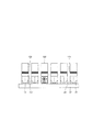
前記第1の基板上に、主として酸化ケイ素から成る第1の層を形成する工程と、
前記第1の層を部分的に除去して前記第1の基板の露出部を形成する工程と、
前記露出部を持つ第1の基板上に、非晶質窒化ガリウム系化合物半導体を堆積する工程と、
前記第1の層上の前記非晶質窒化ガリウム系化合物半導体を蒸発させ、前記第1の基板の露出部上に前記非晶質窒化ガリウム系化合物半導体の核を形成する工程と、
前記非晶質窒化ガリウム系化合物半導体の核から、前記第1の基板上に窒化ガリウム系化合物半導体のエピタキシャル層を形成する工程と、
前記第1の基板の露出部上の前記窒化ガリウム系化合物半導体のエピタキシャル層を除去して分離溝を形成する工程と、
を含むことを特徴とする窒化ガリウム系化合物半導体層の形成方法。 A method for forming a gallium nitride compound semiconductor layer comprising epitaxially growing a gallium nitride compound semiconductor on a first substrate which is a sapphire substrate or a SiC substrate, and forming a layer,
Forming a first layer mainly composed of silicon oxide on the first substrate;
Partially removing the first layer to form an exposed portion of the first substrate;
Depositing an amorphous gallium nitride compound semiconductor on the first substrate having the exposed portion;
Evaporating the amorphous gallium nitride compound semiconductor on the first layer to form a nucleus of the amorphous gallium nitride compound semiconductor on an exposed portion of the first substrate;
Forming an epitaxial layer of a gallium nitride compound semiconductor on the first substrate from the nucleus of the amorphous gallium nitride compound semiconductor;
Removing the epitaxial layer of the gallium nitride compound semiconductor on the exposed portion of the first substrate to form a separation groove;
A method for forming a gallium nitride-based compound semiconductor layer, comprising:
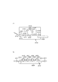
前記第1の基板上の第1の層の端部を表出させる工程と、
処理により分離可能状態となる分離層を表面に有し貫通溝が存在する第2の基板を用意する工程と、
前記分離層を介して前記第1の基板と前記第2の基板を貼り合わせる工程と、
前記貼り合わせた第1の基板と第2の基板をエッチング液に浸潤してエッチング液を前記貫通溝と前記分離溝を通して前記第1の層と接触させることにより、前記第1の層を選択的にエッチングして前記第1の基板上の前記エピタキシャル層を前記第2の基板に移設する工程と、
前記第2の基板に移設された前記エピタキシャル層の少なくとも一部を第3の基板に接合し、前記第2の基板と前記エピタキシャル層を前記分離層で分離して前記エピタキシャル層を前記第2の基板から前記第3の基板に移設する工程と、
を含むことを特徴とする移設方法。 A transfer method for transferring a gallium nitride compound semiconductor layer on a first substrate obtained by the method for forming a gallium nitride compound semiconductor layer according to claim 1 or 2 to another substrate,
Exposing the edge of the first layer on the first substrate;
Preparing a second substrate having a separation layer on its surface and having a through-groove that becomes separable by processing; and
Bonding the first substrate and the second substrate through the separation layer;
The first layer and the second substrate bonded together are infiltrated into an etching solution, and the etching solution is brought into contact with the first layer through the through groove and the separation groove, thereby selectively selecting the first layer. Etching to transfer the epitaxial layer on the first substrate to the second substrate;
At least a part of the epitaxial layer transferred to the second substrate is bonded to a third substrate, the second substrate and the epitaxial layer are separated by the separation layer, and the epitaxial layer is separated from the second substrate. Transferring from the substrate to the third substrate;
Relocation method characterized by including.
前記分離層は、光の照射により分解又は結合強度が低下する材料を含み、
前記移設されるエピタキシャル層と前記第2の基板との間の前記分離層に光の照射を行って前記移設されるエピタキシャル層と前記第2の基板を前記分離層で分離することを特徴とする請求項3から7のいずれか1項に記載の移設方法。 The second substrate has translucency;
The separation layer includes a material whose decomposition or bond strength is reduced by light irradiation,
The separation layer between the transferred epitaxial layer and the second substrate is irradiated with light to separate the transferred epitaxial layer and the second substrate with the separation layer. The relocation method according to any one of claims 3 to 7.
前記移設されるエピタキシャル層と前記第2の基板との間の前記分離層を加熱又は冷却して前記移設されるエピタキシャル層と前記第2の基板を前記分離層で分離することを特徴とする請求項3から7のいずれか1項に記載の移設方法。 The separation layer includes a material whose decomposition or bond strength is reduced by heating or cooling,
The separation layer between the transferred epitaxial layer and the second substrate is heated or cooled to separate the transferred epitaxial layer and the second substrate with the separation layer. Item 8. The relocation method according to any one of Items 3 to 7.
前記LEDプリンタヘッドを光源として、前記感光ドラムに静電潜像を書き込む作像ユニットを備えることを特徴とするLEDプリンタ。 An LED printer head including the LED array according to claim 13 or an LED printer head according to claim 14 , a photosensitive drum, and a charger.
An LED printer comprising: an image forming unit for writing an electrostatic latent image on the photosensitive drum using the LED printer head as a light source.
前記LEDプリンタヘッドを光源として、前記感光ドラムに静電潜像を書き込む作像ユニットを複数備えることを特徴とするカラーLEDプリンタ。 An LED printer head including the LED array according to claim 13 or an LED printer head according to claim 14 , a photosensitive drum, and a charger.
A color LED printer comprising a plurality of image forming units for writing an electrostatic latent image on the photosensitive drum using the LED printer head as a light source.
Priority Applications (5)
| Application Number | Priority Date | Filing Date | Title |
|---|---|---|---|
| JP2008282794A JP5132524B2 (en) | 2008-11-04 | 2008-11-04 | Method of transferring gallium nitride compound semiconductor layer and substrate bonded with gallium nitride compound semiconductor layer |
| EP09013630A EP2182547A2 (en) | 2008-11-04 | 2009-10-29 | Forming method of gallium nitride system compound semiconductor layer, transfer method of the same, and substrate structure with the same bonded thereto |
| KR1020090104802A KR101200804B1 (en) | 2008-11-04 | 2009-11-02 | Forming method of gallium nitride system compound semiconductor layer, transfer method of the same, and substrate structure with the same bonded thereto |
| US12/611,791 US8053335B2 (en) | 2008-11-04 | 2009-11-03 | Forming method of gallium nitride system compound semiconductor layer, transfer method of the same, and substrate structure with the same bonded thereto |
| CN200910211516XA CN101740697B (en) | 2008-11-04 | 2009-11-04 | Forming method of gallium nitride system compound semiconductor layer, transfer method of the same, and substrate structure |
Applications Claiming Priority (1)
| Application Number | Priority Date | Filing Date | Title |
|---|---|---|---|
| JP2008282794A JP5132524B2 (en) | 2008-11-04 | 2008-11-04 | Method of transferring gallium nitride compound semiconductor layer and substrate bonded with gallium nitride compound semiconductor layer |
Publications (3)
| Publication Number | Publication Date |
|---|---|
| JP2010114112A JP2010114112A (en) | 2010-05-20 |
| JP2010114112A5 true JP2010114112A5 (en) | 2011-12-22 |
| JP5132524B2 JP5132524B2 (en) | 2013-01-30 |
Family
ID=41479123
Family Applications (1)
| Application Number | Title | Priority Date | Filing Date |
|---|---|---|---|
| JP2008282794A Expired - Fee Related JP5132524B2 (en) | 2008-11-04 | 2008-11-04 | Method of transferring gallium nitride compound semiconductor layer and substrate bonded with gallium nitride compound semiconductor layer |
Country Status (5)
| Country | Link |
|---|---|
| US (1) | US8053335B2 (en) |
| EP (1) | EP2182547A2 (en) |
| JP (1) | JP5132524B2 (en) |
| KR (1) | KR101200804B1 (en) |
| CN (1) | CN101740697B (en) |
Families Citing this family (21)
| Publication number | Priority date | Publication date | Assignee | Title |
|---|---|---|---|---|
| US8860183B2 (en) | 2009-06-10 | 2014-10-14 | Seoul Viosys Co., Ltd. | Semiconductor substrate, semiconductor device, and manufacturing methods thereof |
| US8481411B2 (en) * | 2009-06-10 | 2013-07-09 | Seoul Opto Device Co., Ltd. | Method of manufacturing a semiconductor substrate having a cavity |
| KR101998885B1 (en) | 2010-05-31 | 2019-07-10 | 니치아 카가쿠 고교 가부시키가이샤 | Light-emitting device and manufacturing method therefor |
| KR101702943B1 (en) * | 2010-10-29 | 2017-02-22 | 엘지이노텍 주식회사 | Fabrication method of light emitting device |
| CN102468318B (en) * | 2010-11-04 | 2014-12-24 | 上海蓝光科技有限公司 | Chip structure of high-voltage direct current light emitting diode and method for manufacturing chip structure |
| US8841207B2 (en) | 2011-04-08 | 2014-09-23 | Lux Material Co., Ltd. | Reusable substrates for electronic device fabrication and methods thereof |
| US9306117B2 (en) | 2011-07-25 | 2016-04-05 | Industrial Technology Research Institute | Transfer-bonding method for light emitting devices |
| CN103378236B (en) * | 2012-04-25 | 2017-04-05 | 清华大学 | epitaxial structure with micro-structure |
| US9196606B2 (en) * | 2013-01-09 | 2015-11-24 | Nthdegree Technologies Worldwide Inc. | Bonding transistor wafer to LED wafer to form active LED modules |
| JP6315852B2 (en) * | 2013-12-23 | 2018-04-25 | インテル・コーポレーション | Semiconductor transistor structure, system-on-chip, and semiconductor transistor structure forming method |
| US10032911B2 (en) | 2013-12-23 | 2018-07-24 | Intel Corporation | Wide band gap transistor on non-native semiconductor substrate |
| KR101574267B1 (en) | 2013-12-23 | 2015-12-04 | 주식회사 글로벌식스 | Supporting substrate for light eimming device and method of manufacturing a light emitting device using the same |
| KR102139681B1 (en) | 2014-01-29 | 2020-07-30 | 휴렛-팩커드 디벨롭먼트 컴퍼니, 엘.피. | Light-emitting element array module and method for controlling Light-emitting element array chips |
| US9508545B2 (en) | 2015-02-09 | 2016-11-29 | Applied Materials, Inc. | Selectively lateral growth of silicon oxide thin film |
| JP6799007B2 (en) * | 2015-05-21 | 2020-12-09 | エーファウ・グループ・エー・タルナー・ゲーエムベーハー | How to apply a growth layer on the seed layer |
| KR101787435B1 (en) * | 2016-02-29 | 2017-10-19 | 피에스아이 주식회사 | Method for manufacturing nanorods |
| US11749790B2 (en) | 2017-12-20 | 2023-09-05 | Lumileds Llc | Segmented LED with embedded transistors |
| WO2020076452A1 (en) | 2018-10-10 | 2020-04-16 | Glo Ab | Vertical stacks of light emitting diodes and control transistors and method of making thereof |
| JP7276221B2 (en) * | 2020-03-25 | 2023-05-18 | 信越半導体株式会社 | Bonded wafer manufacturing method and bonded wafer |
| US11552710B2 (en) * | 2020-08-17 | 2023-01-10 | Acacia Communications, Inc. | Resistivity engineered substrate for RF common-mode suppression |
| JPWO2022210402A1 (en) * | 2021-03-31 | 2022-10-06 |
Family Cites Families (19)
| Publication number | Priority date | Publication date | Assignee | Title |
|---|---|---|---|---|
| JP2628404B2 (en) | 1990-10-25 | 1997-07-09 | 日亜化学工業株式会社 | Semiconductor crystal film growth method |
| US5433169A (en) * | 1990-10-25 | 1995-07-18 | Nichia Chemical Industries, Ltd. | Method of depositing a gallium nitride-based III-V group compound semiconductor crystal layer |
| US5334277A (en) * | 1990-10-25 | 1994-08-02 | Nichia Kagaky Kogyo K.K. | Method of vapor-growing semiconductor crystal and apparatus for vapor-growing the same |
| US6071795A (en) | 1998-01-23 | 2000-06-06 | The Regents Of The University Of California | Separation of thin films from transparent substrates by selective optical processing |
| JP3510479B2 (en) * | 1998-04-27 | 2004-03-29 | シャープ株式会社 | Manufacturing method of optical input / output element array device |
| JP2002270516A (en) * | 2001-03-07 | 2002-09-20 | Nec Corp | Growing method of iii group nitride semiconductor, film thereof and semiconductor element using the same |
| JP2003077940A (en) * | 2001-09-06 | 2003-03-14 | Sony Corp | Method of transferring device, method of arranging device using same, and method of manufacturing image display device unit |
| WO2003038957A1 (en) * | 2001-10-29 | 2003-05-08 | Sharp Kabushiki Kaisha | Nitride semiconductor device, its manufacturing method, and semiconductor optical apparatus |
| CN1242091C (en) * | 2002-12-20 | 2006-02-15 | 上海北大蓝光科技有限公司 | Method for growing epitaxial chip of nitride LED structure by MOCVD |
| JP4056481B2 (en) * | 2003-02-07 | 2008-03-05 | 三洋電機株式会社 | Semiconductor device and manufacturing method thereof |
| TWI328837B (en) * | 2003-02-28 | 2010-08-11 | Semiconductor Energy Lab | Semiconductor device and method of manufacturing the same |
| US6986693B2 (en) * | 2003-03-26 | 2006-01-17 | Lucent Technologies Inc. | Group III-nitride layers with patterned surfaces |
| CN100502018C (en) * | 2004-02-06 | 2009-06-17 | 株式会社半导体能源研究所 | Method for manufacturing thin-film semiconductor circuit, and element substrate |
| JP2006156802A (en) * | 2004-11-30 | 2006-06-15 | Showa Denko Kk | Group iii nitride semiconductor device |
| JP4848638B2 (en) * | 2005-01-13 | 2011-12-28 | ソニー株式会社 | Method for forming semiconductor device and method for mounting semiconductor device |
| JP2006222402A (en) | 2005-02-14 | 2006-08-24 | Toshiba Ceramics Co Ltd | Gallium nitride system compound semiconductor and method for manufacturing the same |
| JP4462249B2 (en) * | 2005-09-22 | 2010-05-12 | ソニー株式会社 | Light emitting diode manufacturing method, integrated light emitting diode manufacturing method, and nitride III-V compound semiconductor growth method |
| JP4910608B2 (en) * | 2006-10-02 | 2012-04-04 | ソニー株式会社 | Light emitting diode manufacturing method and electronic device manufacturing method |
| JP5171016B2 (en) * | 2006-10-27 | 2013-03-27 | キヤノン株式会社 | Semiconductor member, manufacturing method of semiconductor article, and LED array using the manufacturing method |
-
2008
- 2008-11-04 JP JP2008282794A patent/JP5132524B2/en not_active Expired - Fee Related
-
2009
- 2009-10-29 EP EP09013630A patent/EP2182547A2/en not_active Withdrawn
- 2009-11-02 KR KR1020090104802A patent/KR101200804B1/en not_active IP Right Cessation
- 2009-11-03 US US12/611,791 patent/US8053335B2/en not_active Expired - Fee Related
- 2009-11-04 CN CN200910211516XA patent/CN101740697B/en not_active Expired - Fee Related
Similar Documents
| Publication | Publication Date | Title |
|---|---|---|
| JP2010114112A5 (en) | ||
| TWI605546B (en) | Method of manufacturing semiconductor device array | |
| JP5132524B2 (en) | Method of transferring gallium nitride compound semiconductor layer and substrate bonded with gallium nitride compound semiconductor layer | |
| US8030666B2 (en) | Group-III nitride epitaxial layer on silicon substrate | |
| TWI463558B (en) | Solid state lighting devices and associated methods of manufacturing | |
| US8501582B2 (en) | Semiconductor structure having low thermal stress and method for manufacturing thereof | |
| JP2018535536A (en) | System and method for graphene-based layer transfer | |
| JP2009038344A5 (en) | ||
| US20170133295A1 (en) | Semiconductor device with high thermal conductivity substrate and process for making the same | |
| JP2010056458A (en) | Method of manufacturing light emitting element | |
| JP2017119624A (en) | Substrate for semiconductor device | |
| CN103985796A (en) | Electronic device | |
| US7510906B2 (en) | Diamond substrate and method for fabricating the same | |
| JP2006196693A (en) | Method for forming semiconductor device and method for mounting semiconductor device | |
| JP2010114104A5 (en) | ||
| KR101878754B1 (en) | Method of manufacturing large area gallium nitride substrate | |
| JP2012054559A5 (en) | ||
| JP2013517621A (en) | Semiconductor light emitting device comprising a layer for compensating for thermal expansion of a substrate | |
| JP2018095545A (en) | Ramo4 substrate and production method of iii group nitride crystal | |
| WO2013078950A1 (en) | Semiconductor structure and method for forming the same | |
| Lee et al. | A discrete core-shell-like micro-light-emitting diode array grown on sapphire nano-membranes | |
| JP2005129825A5 (en) | ||
| WO2014071879A1 (en) | Method for separating light emitting diode substrate | |
| US9577031B2 (en) | Semiconductor structure and method for forming the same | |
| CN105826438A (en) | Light-emitting diode with metal buffer layer and preparation method thereof |