JP2010086377A - 入力装置および表示装置 - Google Patents
入力装置および表示装置 Download PDFInfo
- Publication number
- JP2010086377A JP2010086377A JP2008256060A JP2008256060A JP2010086377A JP 2010086377 A JP2010086377 A JP 2010086377A JP 2008256060 A JP2008256060 A JP 2008256060A JP 2008256060 A JP2008256060 A JP 2008256060A JP 2010086377 A JP2010086377 A JP 2010086377A
- Authority
- JP
- Japan
- Prior art keywords
- signal
- output
- input
- display
- circuit
- Prior art date
- Legal status (The legal status is an assumption and is not a legal conclusion. Google has not performed a legal analysis and makes no representation as to the accuracy of the status listed.)
- Granted
Links
Images


Classifications
-
- G—PHYSICS
- G06—COMPUTING OR CALCULATING; COUNTING
- G06F—ELECTRIC DIGITAL DATA PROCESSING
- G06F3/00—Input arrangements for transferring data to be processed into a form capable of being handled by the computer; Output arrangements for transferring data from processing unit to output unit, e.g. interface arrangements
- G06F3/01—Input arrangements or combined input and output arrangements for interaction between user and computer
- G06F3/03—Arrangements for converting the position or the displacement of a member into a coded form
- G06F3/041—Digitisers, e.g. for touch screens or touch pads, characterised by the transducing means
- G06F3/0412—Digitisers structurally integrated in a display
-
- G—PHYSICS
- G06—COMPUTING OR CALCULATING; COUNTING
- G06F—ELECTRIC DIGITAL DATA PROCESSING
- G06F3/00—Input arrangements for transferring data to be processed into a form capable of being handled by the computer; Output arrangements for transferring data from processing unit to output unit, e.g. interface arrangements
- G06F3/01—Input arrangements or combined input and output arrangements for interaction between user and computer
- G06F3/03—Arrangements for converting the position or the displacement of a member into a coded form
- G06F3/041—Digitisers, e.g. for touch screens or touch pads, characterised by the transducing means
- G06F3/042—Digitisers, e.g. for touch screens or touch pads, characterised by the transducing means by opto-electronic means
-
- G—PHYSICS
- G06—COMPUTING OR CALCULATING; COUNTING
- G06F—ELECTRIC DIGITAL DATA PROCESSING
- G06F3/00—Input arrangements for transferring data to be processed into a form capable of being handled by the computer; Output arrangements for transferring data from processing unit to output unit, e.g. interface arrangements
- G06F3/01—Input arrangements or combined input and output arrangements for interaction between user and computer
- G06F3/03—Arrangements for converting the position or the displacement of a member into a coded form
- G06F3/041—Digitisers, e.g. for touch screens or touch pads, characterised by the transducing means
- G06F3/047—Digitisers, e.g. for touch screens or touch pads, characterised by the transducing means using sets of wires, e.g. crossed wires
Landscapes
- Engineering & Computer Science (AREA)
- General Engineering & Computer Science (AREA)
- Theoretical Computer Science (AREA)
- Human Computer Interaction (AREA)
- Physics & Mathematics (AREA)
- General Physics & Mathematics (AREA)
- Position Input By Displaying (AREA)
- Control Of Indicators Other Than Cathode Ray Tubes (AREA)
- Liquid Crystal (AREA)
Abstract
【解決手段】I/Oパネル11内に設けられたタッチ検出回路15において、全てのセンサ素子11Bからの出力信号11Cが入力される前に、既にセンサ素子11Bから入力された出力信号からオン信号の有無が判別され、その判別結果が出力信号18Aとして、I/Oパネル11とは別体で設けられた外部処理部20のアプリケーションプログラム実行部22に出力される。
【選択図】図1
Description
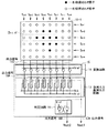
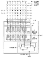
図1は、本発明の第一の実施の形態に係る表示装置1の全体構成を表すものである。本実施の形態の表示装置1は、表面に接触した物体(検出対称物)の接触情報などを読み取る入力機能を備えた表示装置である。この表示装置1は、表示部10と、表示部10とは別体に設けられた外部処理部20と、これらの間の信号を伝送する信号伝送部30とを備えている。なお、本発明の一実施の形態に係る入力装置は、上記表示装置1により具現化されるので、以下、合わせて説明する。
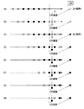
上記実施の形態では、タッチ検出回路15は、複数のセンサ素子11Bのうち一の行に配置された全てのセンサ素子11Bの出力信号11Cから得られた出力信号17Aが一つずつ直列に入力される度に、判別結果を出力信号18Aとして出力していたが、他のタイミングで、判別結果を出力信号18Aとして出力することも可能である。他のタイミングで、判別結果を出力信号18Aとして出力するためには、例えば、図5に示したように、判定回路18の出力段に、スイッチ素子18Bを設ければよい。そのようにした場合に、例えば、図6(A)〜(H)、図7(A)〜(E)に示したように、複数のセンサ素子11Bのうち一の行に配置された全てのセンサ素子11Bの出力信号から得られた出力信号17Aが全て入力されたのちに、スイッチ素子18Bを、スイッチ素子18Bに接続されたクロック線に印加する信号Vsr−ckをオンオフし、信号Vsr−ckのオンオフに同期して、判別結果を出力信号18Aとして出力してもよい。
図9は、本発明の第二の実施の形態に係る表示装置2の全体構成を表すものである。この表示装置2は、表示部10にタッチ検出回路45を有している点で、表示部10にタッチ検出回路15を有する表示装置1の構成と相違する。そこで、以下では、上記実施の形態との相違点について主に説明し、上記実施の形態との共通点についての説明を適宜省略するものとする。
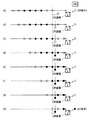
上記第二の実施の形態では、並列入力直列出力回路47は、複数のセンサ素子11Bのうち互いに隣接する2つの行に配置された全てのセンサ素子11Bの出力信号11Cから得られた出力信号47Aを2×2のマトリクスで後段の判定回路48に出力するようになっていた。しかし、並列入力直列出力回路47は、出力信号47Aを3×3のマトリクスで後段の判定回路48に出力するようになっていてもよい。ただし、その場合には、判定回路48は、例えば、並列入力直列出力回路47から3×3のマトリクスで順次入力される出力信号47Aのうち3×3のマトリクスにおいて互いに隣り合う3つの出力信号17Aの全てがオン信号に該当するか否かを判定する回路を含んで構成されていることが好ましい。
Claims (6)
- 行方向および列方向に2次元配置された複数のセンサ素子と、前記複数のセンサ素子を駆動する駆動回路と、前記複数のセンサ素子からの出力信号を処理する処理回路とが設けられたパネルを備え、
前記処理回路は、前記パネルの表面に接触または近接する物体の影響を受けた出力信号をオン信号とすると、前記全てのセンサ素子からの出力信号が入力される前に、既に入力された出力信号から前記オン信号の有無を判別し、その判別結果を出力する入力装置。 - 前記処理回路は、前記複数のセンサ素子のうち少なくとも一の行に配置された全てのセンサ素子の出力信号から得られた信号が一つずつ入力される度に、前記判別結果を出力する請求項1に記載の入力装置。
- 前記処理回路は、前記複数のセンサ素子のうち少なくとも一の行に配置された全てのセンサ素子の出力信号から得られた信号が全て入力されたのちに、前記判別結果を出力する請求項1に記載の入力装置。
- 前記パネルとは別体で設けられた外部処理部と、
前記パネルと前記外部処理部との間の信号を伝送する信号伝送部と
を備え、
前記処理回路は、前記判別結果を前記外部処理部に出力する請求項1に記載の入力装置。 - 前記処理回路は、前記複数のセンサ素子のうち少なくとも一の行に配置された全てのセンサ素子から入力された出力信号から、前記オン信号の数をカウントすると共に、前記オン信号の位置についての情報を導出し、前記オン信号の数および前記オン信号の位置についての情報を出力する請求項1ないし請求項4の少なくとも一項に記載の入力装置。
- 行方向および列方向に2次元配置された複数の表示画素および複数のセンサ素子と、前記複数の表示画素および前記複数のセンサ素子を駆動する駆動回路と、前記複数のセンサ素子からの出力信号を処理する処理回路とが設けられたパネルを備え、
前記処理回路は、前記パネルの表面に接触または近接する物体の影響を受けた出力信号をオン信号とすると、前記全てのセンサ素子からの出力信号が入力される前に、既に入力された出力信号から前記オン信号の有無を判別し、その判別結果を出力する表示装置。
Priority Applications (4)
| Application Number | Priority Date | Filing Date | Title |
|---|---|---|---|
| JP2008256060A JP5252427B2 (ja) | 2008-10-01 | 2008-10-01 | 入力装置および表示装置 |
| TW098130137A TWI404999B (zh) | 2008-10-01 | 2009-09-07 | 輸入裝置及顯示器 |
| US12/557,289 US20100079394A1 (en) | 2008-10-01 | 2009-09-10 | Input device and display |
| CN2009101794182A CN101714038B (zh) | 2008-10-01 | 2009-10-09 | 输入装置和显示器 |
Applications Claiming Priority (1)
| Application Number | Priority Date | Filing Date | Title |
|---|---|---|---|
| JP2008256060A JP5252427B2 (ja) | 2008-10-01 | 2008-10-01 | 入力装置および表示装置 |
Publications (2)
| Publication Number | Publication Date |
|---|---|
| JP2010086377A true JP2010086377A (ja) | 2010-04-15 |
| JP5252427B2 JP5252427B2 (ja) | 2013-07-31 |
Family
ID=42056874
Family Applications (1)
| Application Number | Title | Priority Date | Filing Date |
|---|---|---|---|
| JP2008256060A Expired - Fee Related JP5252427B2 (ja) | 2008-10-01 | 2008-10-01 | 入力装置および表示装置 |
Country Status (4)
| Country | Link |
|---|---|
| US (1) | US20100079394A1 (ja) |
| JP (1) | JP5252427B2 (ja) |
| CN (1) | CN101714038B (ja) |
| TW (1) | TWI404999B (ja) |
Cited By (1)
| Publication number | Priority date | Publication date | Assignee | Title |
|---|---|---|---|---|
| JP2017501462A (ja) * | 2013-10-04 | 2017-01-12 | マイクロチップ テクノロジー インコーポレイテッドMicrochip Technology Incorporated | 多重チャネル容量分圧器走査方法および装置 |
Families Citing this family (10)
| Publication number | Priority date | Publication date | Assignee | Title |
|---|---|---|---|---|
| US8963852B2 (en) * | 2010-08-20 | 2015-02-24 | Innolux Corporation | Touch panel, driving method for the touch panel, program for getting touch information, and memory media |
| KR101329461B1 (ko) * | 2010-11-25 | 2013-11-15 | 엘지디스플레이 주식회사 | 터치 스크린 패널 일체형 표시장치 |
| US9015682B1 (en) | 2012-03-28 | 2015-04-21 | Google Inc. | Computer code transformations to create synthetic global scopes |
| US20150205585A1 (en) * | 2012-06-04 | 2015-07-23 | Google Inc. | Delayed compiling of scripting language code |
| US9383840B2 (en) * | 2013-04-22 | 2016-07-05 | Samsung Display Co., Ltd. | Method and apparatus to reduce display lag using image overlay |
| TWI507957B (zh) * | 2013-07-22 | 2015-11-11 | Chunghwa Picture Tubes Ltd | 驅動觸控顯示器的方法及提升訊雜比的觸控顯示器 |
| KR102171389B1 (ko) * | 2014-04-21 | 2020-10-30 | 삼성디스플레이 주식회사 | 영상 표시 시스템 |
| KR102206047B1 (ko) | 2014-09-15 | 2021-01-21 | 삼성디스플레이 주식회사 | 단말 및 디스플레이 지연 감소 방법 및 장치 |
| KR20170085050A (ko) * | 2014-11-18 | 2017-07-21 | 텍추얼 랩스 컴퍼니 | 인터 모듈 통신을 위한 시스템 및 방법 |
| CN107238742A (zh) * | 2017-04-24 | 2017-10-10 | 天津瑞能电气有限公司 | 兆瓦级微电网并离网切换暂态监测系统 |
Citations (6)
| Publication number | Priority date | Publication date | Assignee | Title |
|---|---|---|---|---|
| JPS5920348U (ja) * | 1982-07-28 | 1984-02-07 | オムロン株式会社 | 透視型指タツチ入力装置 |
| JPS63172325A (ja) * | 1987-01-10 | 1988-07-16 | Pioneer Electronic Corp | タツチパネル制御装置 |
| JPH07271511A (ja) * | 1994-03-28 | 1995-10-20 | Hitachi Software Eng Co Ltd | 感圧式タブレットおよび情報処理装置 |
| JPH09274538A (ja) * | 1996-04-05 | 1997-10-21 | Digital:Kk | マトリックス型タッチパネル入力装置 |
| JP2007087393A (ja) * | 2005-09-21 | 2007-04-05 | Samsung Electronics Co Ltd | 表示装置とその駆動方法及び駆動装置 |
| JP2007128497A (ja) * | 2005-10-05 | 2007-05-24 | Sony Corp | 表示装置および表示方法 |
Family Cites Families (5)
| Publication number | Priority date | Publication date | Assignee | Title |
|---|---|---|---|---|
| JP2001075074A (ja) * | 1999-08-18 | 2001-03-23 | Internatl Business Mach Corp <Ibm> | タッチセンサ一体型液晶表示素子 |
| US7100141B1 (en) * | 2003-12-23 | 2006-08-29 | Altera Corporation | Technology mapping technique for fracturable logic elements |
| KR101160828B1 (ko) * | 2004-12-23 | 2012-06-29 | 삼성전자주식회사 | 표시 장치, 그 구동 방법 및 표시 장치용 구동 장치 |
| US20070182723A1 (en) * | 2006-01-31 | 2007-08-09 | Toshiba Matsushita Display Technology Co., Ltd. | Display device |
| KR101303881B1 (ko) * | 2006-08-03 | 2013-09-04 | 삼성디스플레이 주식회사 | 터치 스크린, 그 제조 방법 및 이를 구비하는 표시 장치 |
-
2008
- 2008-10-01 JP JP2008256060A patent/JP5252427B2/ja not_active Expired - Fee Related
-
2009
- 2009-09-07 TW TW098130137A patent/TWI404999B/zh not_active IP Right Cessation
- 2009-09-10 US US12/557,289 patent/US20100079394A1/en not_active Abandoned
- 2009-10-09 CN CN2009101794182A patent/CN101714038B/zh not_active Expired - Fee Related
Patent Citations (6)
| Publication number | Priority date | Publication date | Assignee | Title |
|---|---|---|---|---|
| JPS5920348U (ja) * | 1982-07-28 | 1984-02-07 | オムロン株式会社 | 透視型指タツチ入力装置 |
| JPS63172325A (ja) * | 1987-01-10 | 1988-07-16 | Pioneer Electronic Corp | タツチパネル制御装置 |
| JPH07271511A (ja) * | 1994-03-28 | 1995-10-20 | Hitachi Software Eng Co Ltd | 感圧式タブレットおよび情報処理装置 |
| JPH09274538A (ja) * | 1996-04-05 | 1997-10-21 | Digital:Kk | マトリックス型タッチパネル入力装置 |
| JP2007087393A (ja) * | 2005-09-21 | 2007-04-05 | Samsung Electronics Co Ltd | 表示装置とその駆動方法及び駆動装置 |
| JP2007128497A (ja) * | 2005-10-05 | 2007-05-24 | Sony Corp | 表示装置および表示方法 |
Cited By (2)
| Publication number | Priority date | Publication date | Assignee | Title |
|---|---|---|---|---|
| JP2017501462A (ja) * | 2013-10-04 | 2017-01-12 | マイクロチップ テクノロジー インコーポレイテッドMicrochip Technology Incorporated | 多重チャネル容量分圧器走査方法および装置 |
| US10408862B2 (en) | 2013-10-04 | 2019-09-10 | Microchip Technology Incorporated | Multiple channel capacitive voltage divider scanning method and apparatus |
Also Published As
| Publication number | Publication date |
|---|---|
| CN101714038A (zh) | 2010-05-26 |
| CN101714038B (zh) | 2012-11-07 |
| US20100079394A1 (en) | 2010-04-01 |
| TWI404999B (zh) | 2013-08-11 |
| JP5252427B2 (ja) | 2013-07-31 |
| TW201022781A (en) | 2010-06-16 |
Similar Documents
| Publication | Publication Date | Title |
|---|---|---|
| JP5252427B2 (ja) | 入力装置および表示装置 | |
| US10748476B2 (en) | Display panel, method for driving the same, and display device | |
| CN108664895B (zh) | 显示装置及其指纹识别方法 | |
| JP4257221B2 (ja) | 表示装置および情報端末装置 | |
| US8797275B2 (en) | Display apparatus and image pickup apparatus | |
| CN102687102B (zh) | 具备光传感器的显示装置 | |
| WO2017206558A1 (zh) | 显示装置及其指纹识别方法 | |
| US11249598B2 (en) | Integrated fingerprint detection touch control display apparatus and integrated method of fingerprint detection, touch control, and image display | |
| JP2009217461A (ja) | 表示装置および位置検出方法 | |
| US10754471B2 (en) | Touch sensing device and image display device using the same | |
| CN104808867A (zh) | 一种内嵌触摸显示屏及触摸显示系统 | |
| TWI614652B (zh) | 具有內建觸控螢幕之顯示面板及包含該顯示面板的觸控顯示裝置 | |
| CN112346588B (zh) | 触控检测方法、驱动器及触控显示装置 | |
| CN111797673A (zh) | 驱动装置及其操作方法 | |
| CN209281372U (zh) | 电子设备 | |
| CN111651083B (zh) | 触摸显示屏的控制方法及控制装置、显示设备 | |
| CN107958650B (zh) | 生物感测模组及其驱动电路、电子设备 | |
| KR20220150970A (ko) | 지문 감지 기능을 갖는 전자 디바이스 | |
| US10963091B2 (en) | Touch panel control apparatus, touch panel control method, and input display apparatus | |
| US20160117040A1 (en) | Touch display apparatus and method for detecting touch point thereof | |
| CN209708138U (zh) | 生物感测模组及其驱动电路、电子设备 | |
| CN113257207B (zh) | 场序液晶显示装置 | |
| JPH04337824A (ja) | 表示一体型タブレット | |
| JP2007047991A (ja) | 表示装置及び表示方法 | |
| TW201928640A (zh) | 光學觸控系統 |
Legal Events
| Date | Code | Title | Description |
|---|---|---|---|
| A621 | Written request for application examination |
Free format text: JAPANESE INTERMEDIATE CODE: A621 Effective date: 20110926 |
|
| A711 | Notification of change in applicant |
Free format text: JAPANESE INTERMEDIATE CODE: A711 Effective date: 20120330 |
|
| A977 | Report on retrieval |
Free format text: JAPANESE INTERMEDIATE CODE: A971007 Effective date: 20120718 |
|
| A131 | Notification of reasons for refusal |
Free format text: JAPANESE INTERMEDIATE CODE: A131 Effective date: 20120724 |
|
| A521 | Written amendment |
Free format text: JAPANESE INTERMEDIATE CODE: A523 Effective date: 20120919 |
|
| TRDD | Decision of grant or rejection written | ||
| A01 | Written decision to grant a patent or to grant a registration (utility model) |
Free format text: JAPANESE INTERMEDIATE CODE: A01 Effective date: 20130319 |
|
| RD03 | Notification of appointment of power of attorney |
Free format text: JAPANESE INTERMEDIATE CODE: A7423 Effective date: 20130328 |
|
| A61 | First payment of annual fees (during grant procedure) |
Free format text: JAPANESE INTERMEDIATE CODE: A61 Effective date: 20130409 |
|
| R150 | Certificate of patent or registration of utility model |
Free format text: JAPANESE INTERMEDIATE CODE: R150 |
|
| FPAY | Renewal fee payment (event date is renewal date of database) |
Free format text: PAYMENT UNTIL: 20160426 Year of fee payment: 3 |
|
| LAPS | Cancellation because of no payment of annual fees |