JP2010062548A - Semiconductor device and method of manufacturing the same - Google Patents
Semiconductor device and method of manufacturing the same Download PDFInfo
- Publication number
- JP2010062548A JP2010062548A JP2009181705A JP2009181705A JP2010062548A JP 2010062548 A JP2010062548 A JP 2010062548A JP 2009181705 A JP2009181705 A JP 2009181705A JP 2009181705 A JP2009181705 A JP 2009181705A JP 2010062548 A JP2010062548 A JP 2010062548A
- Authority
- JP
- Japan
- Prior art keywords
- layer
- semiconductor
- thin film
- electrode layer
- film transistor
- Prior art date
- Legal status (The legal status is an assumption and is not a legal conclusion. Google has not performed a legal analysis and makes no representation as to the accuracy of the status listed.)
- Granted
Links
- 239000004065 semiconductor Substances 0.000 title claims abstract description 347
- 238000004519 manufacturing process Methods 0.000 title claims abstract description 33
- 239000010409 thin film Substances 0.000 claims abstract description 252
- 229910052733 gallium Inorganic materials 0.000 claims abstract description 36
- 229910052738 indium Inorganic materials 0.000 claims abstract description 36
- 229910052725 zinc Inorganic materials 0.000 claims abstract description 35
- 239000000758 substrate Substances 0.000 claims description 116
- 238000000034 method Methods 0.000 claims description 101
- 230000015572 biosynthetic process Effects 0.000 claims description 53
- 238000004544 sputter deposition Methods 0.000 claims description 52
- 239000012298 atmosphere Substances 0.000 claims description 38
- 239000011701 zinc Substances 0.000 claims description 34
- 229910052782 aluminium Inorganic materials 0.000 claims description 29
- QVGXLLKOCUKJST-UHFFFAOYSA-N atomic oxygen Chemical compound [O] QVGXLLKOCUKJST-UHFFFAOYSA-N 0.000 claims description 29
- 239000001301 oxygen Substances 0.000 claims description 29
- 229910052760 oxygen Inorganic materials 0.000 claims description 29
- 239000010936 titanium Substances 0.000 claims description 26
- XAGFODPZIPBFFR-UHFFFAOYSA-N aluminium Chemical compound [Al] XAGFODPZIPBFFR-UHFFFAOYSA-N 0.000 claims description 25
- 229910052719 titanium Inorganic materials 0.000 claims description 25
- RTAQQCXQSZGOHL-UHFFFAOYSA-N Titanium Chemical compound [Ti] RTAQQCXQSZGOHL-UHFFFAOYSA-N 0.000 claims description 24
- 239000007789 gas Substances 0.000 claims description 19
- 239000012535 impurity Substances 0.000 claims description 10
- GYHNNYVSQQEPJS-UHFFFAOYSA-N Gallium Chemical compound [Ga] GYHNNYVSQQEPJS-UHFFFAOYSA-N 0.000 claims description 9
- APFVFJFRJDLVQX-UHFFFAOYSA-N indium atom Chemical compound [In] APFVFJFRJDLVQX-UHFFFAOYSA-N 0.000 claims description 9
- HCHKCACWOHOZIP-UHFFFAOYSA-N Zinc Chemical compound [Zn] HCHKCACWOHOZIP-UHFFFAOYSA-N 0.000 claims description 8
- 238000009751 slip forming Methods 0.000 claims description 8
- 239000011777 magnesium Substances 0.000 claims description 7
- 229910052749 magnesium Inorganic materials 0.000 claims description 7
- FYYHWMGAXLPEAU-UHFFFAOYSA-N Magnesium Chemical compound [Mg] FYYHWMGAXLPEAU-UHFFFAOYSA-N 0.000 claims description 5
- 239000010408 film Substances 0.000 abstract description 317
- 239000010410 layer Substances 0.000 description 592
- 239000004973 liquid crystal related substance Substances 0.000 description 47
- 230000008569 process Effects 0.000 description 40
- 239000000463 material Substances 0.000 description 34
- VYPSYNLAJGMNEJ-UHFFFAOYSA-N Silicium dioxide Chemical compound O=[Si]=O VYPSYNLAJGMNEJ-UHFFFAOYSA-N 0.000 description 28
- 230000006870 function Effects 0.000 description 26
- 229910052814 silicon oxide Inorganic materials 0.000 description 25
- 238000010438 heat treatment Methods 0.000 description 24
- 238000012545 processing Methods 0.000 description 24
- 229910052581 Si3N4 Inorganic materials 0.000 description 23
- HQVNEWCFYHHQES-UHFFFAOYSA-N silicon nitride Chemical compound N12[Si]34N5[Si]62N3[Si]51N64 HQVNEWCFYHHQES-UHFFFAOYSA-N 0.000 description 23
- 239000000123 paper Substances 0.000 description 19
- XKRFYHLGVUSROY-UHFFFAOYSA-N Argon Chemical compound [Ar] XKRFYHLGVUSROY-UHFFFAOYSA-N 0.000 description 16
- 238000005401 electroluminescence Methods 0.000 description 16
- 239000011159 matrix material Substances 0.000 description 16
- 230000001681 protective effect Effects 0.000 description 16
- 229910052751 metal Inorganic materials 0.000 description 15
- 239000002184 metal Substances 0.000 description 15
- 239000002245 particle Substances 0.000 description 15
- 125000004429 atom Chemical group 0.000 description 14
- 238000005530 etching Methods 0.000 description 14
- 229920005989 resin Polymers 0.000 description 12
- 239000011347 resin Substances 0.000 description 12
- 238000012546 transfer Methods 0.000 description 11
- IJGRMHOSHXDMSA-UHFFFAOYSA-N Atomic nitrogen Chemical compound N#N IJGRMHOSHXDMSA-UHFFFAOYSA-N 0.000 description 10
- 239000012071 phase Substances 0.000 description 10
- 239000003094 microcapsule Substances 0.000 description 9
- 239000002356 single layer Substances 0.000 description 9
- 229910052786 argon Inorganic materials 0.000 description 8
- 239000004020 conductor Substances 0.000 description 8
- 239000011521 glass Substances 0.000 description 8
- 239000001257 hydrogen Substances 0.000 description 8
- 229910052739 hydrogen Inorganic materials 0.000 description 8
- 239000000203 mixture Substances 0.000 description 8
- 230000003071 parasitic effect Effects 0.000 description 8
- 239000000565 sealant Substances 0.000 description 8
- 229910052710 silicon Inorganic materials 0.000 description 8
- XUIMIQQOPSSXEZ-UHFFFAOYSA-N Silicon Chemical compound [Si] XUIMIQQOPSSXEZ-UHFFFAOYSA-N 0.000 description 7
- 230000005684 electric field Effects 0.000 description 7
- 239000010703 silicon Substances 0.000 description 7
- ZOKXTWBITQBERF-UHFFFAOYSA-N Molybdenum Chemical compound [Mo] ZOKXTWBITQBERF-UHFFFAOYSA-N 0.000 description 6
- KPUWHANPEXNPJT-UHFFFAOYSA-N disiloxane Chemical class [SiH3]O[SiH3] KPUWHANPEXNPJT-UHFFFAOYSA-N 0.000 description 6
- 229910052736 halogen Inorganic materials 0.000 description 6
- 150000002367 halogens Chemical class 0.000 description 6
- AMGQUBHHOARCQH-UHFFFAOYSA-N indium;oxotin Chemical compound [In].[Sn]=O AMGQUBHHOARCQH-UHFFFAOYSA-N 0.000 description 6
- 239000007769 metal material Substances 0.000 description 6
- 229910052750 molybdenum Inorganic materials 0.000 description 6
- 239000011733 molybdenum Substances 0.000 description 6
- -1 oxynitride Chemical class 0.000 description 6
- 238000005268 plasma chemical vapour deposition Methods 0.000 description 6
- 239000000126 substance Substances 0.000 description 6
- 239000002585 base Substances 0.000 description 5
- 238000000151 deposition Methods 0.000 description 5
- 238000003780 insertion Methods 0.000 description 5
- 230000037431 insertion Effects 0.000 description 5
- 239000007788 liquid Substances 0.000 description 5
- 238000001755 magnetron sputter deposition Methods 0.000 description 5
- 230000007246 mechanism Effects 0.000 description 5
- 150000004767 nitrides Chemical class 0.000 description 5
- 229910052757 nitrogen Inorganic materials 0.000 description 5
- 229920003023 plastic Polymers 0.000 description 5
- 239000004033 plastic Substances 0.000 description 5
- PXGOKWXKJXAPGV-UHFFFAOYSA-N Fluorine Chemical compound FF PXGOKWXKJXAPGV-UHFFFAOYSA-N 0.000 description 4
- UFHFLCQGNIYNRP-UHFFFAOYSA-N Hydrogen Chemical compound [H][H] UFHFLCQGNIYNRP-UHFFFAOYSA-N 0.000 description 4
- XEEYBQQBJWHFJM-UHFFFAOYSA-N Iron Chemical compound [Fe] XEEYBQQBJWHFJM-UHFFFAOYSA-N 0.000 description 4
- 239000004642 Polyimide Substances 0.000 description 4
- BOTDANWDWHJENH-UHFFFAOYSA-N Tetraethyl orthosilicate Chemical compound CCO[Si](OCC)(OCC)OCC BOTDANWDWHJENH-UHFFFAOYSA-N 0.000 description 4
- GWEVSGVZZGPLCZ-UHFFFAOYSA-N Titan oxide Chemical compound O=[Ti]=O GWEVSGVZZGPLCZ-UHFFFAOYSA-N 0.000 description 4
- NIXOWILDQLNWCW-UHFFFAOYSA-N acrylic acid group Chemical group C(C=C)(=O)O NIXOWILDQLNWCW-UHFFFAOYSA-N 0.000 description 4
- 239000011575 calcium Substances 0.000 description 4
- 229910052791 calcium Inorganic materials 0.000 description 4
- 229920001940 conductive polymer Polymers 0.000 description 4
- 230000008021 deposition Effects 0.000 description 4
- 230000006866 deterioration Effects 0.000 description 4
- 238000010586 diagram Methods 0.000 description 4
- 239000000945 filler Substances 0.000 description 4
- 229910052731 fluorine Inorganic materials 0.000 description 4
- 239000011737 fluorine Substances 0.000 description 4
- 229910003437 indium oxide Inorganic materials 0.000 description 4
- PJXISJQVUVHSOJ-UHFFFAOYSA-N indium(iii) oxide Chemical compound [O-2].[O-2].[O-2].[In+3].[In+3] PJXISJQVUVHSOJ-UHFFFAOYSA-N 0.000 description 4
- 150000002500 ions Chemical class 0.000 description 4
- QGLKJKCYBOYXKC-UHFFFAOYSA-N nonaoxidotritungsten Chemical compound O=[W]1(=O)O[W](=O)(=O)O[W](=O)(=O)O1 QGLKJKCYBOYXKC-UHFFFAOYSA-N 0.000 description 4
- 229920001721 polyimide Polymers 0.000 description 4
- 239000012798 spherical particle Substances 0.000 description 4
- OGIDPMRJRNCKJF-UHFFFAOYSA-N titanium oxide Inorganic materials [Ti]=O OGIDPMRJRNCKJF-UHFFFAOYSA-N 0.000 description 4
- 229910001930 tungsten oxide Inorganic materials 0.000 description 4
- YVTHLONGBIQYBO-UHFFFAOYSA-N zinc indium(3+) oxygen(2-) Chemical compound [O--].[Zn++].[In+3] YVTHLONGBIQYBO-UHFFFAOYSA-N 0.000 description 4
- 229910000838 Al alloy Inorganic materials 0.000 description 3
- RYGMFSIKBFXOCR-UHFFFAOYSA-N Copper Chemical compound [Cu] RYGMFSIKBFXOCR-UHFFFAOYSA-N 0.000 description 3
- DGAQECJNVWCQMB-PUAWFVPOSA-M Ilexoside XXIX Chemical compound C[C@@H]1CC[C@@]2(CC[C@@]3(C(=CC[C@H]4[C@]3(CC[C@@H]5[C@@]4(CC[C@@H](C5(C)C)OS(=O)(=O)[O-])C)C)[C@@H]2[C@]1(C)O)C)C(=O)O[C@H]6[C@@H]([C@H]([C@@H]([C@H](O6)CO)O)O)O.[Na+] DGAQECJNVWCQMB-PUAWFVPOSA-M 0.000 description 3
- MUBZPKHOEPUJKR-UHFFFAOYSA-N Oxalic acid Chemical compound OC(=O)C(O)=O MUBZPKHOEPUJKR-UHFFFAOYSA-N 0.000 description 3
- XLOMVQKBTHCTTD-UHFFFAOYSA-N Zinc monoxide Chemical compound [Zn]=O XLOMVQKBTHCTTD-UHFFFAOYSA-N 0.000 description 3
- 239000000956 alloy Substances 0.000 description 3
- 230000008901 benefit Effects 0.000 description 3
- 230000000903 blocking effect Effects 0.000 description 3
- 239000003990 capacitor Substances 0.000 description 3
- 238000005229 chemical vapour deposition Methods 0.000 description 3
- KRKNYBCHXYNGOX-UHFFFAOYSA-N citric acid Chemical compound OC(=O)CC(O)(C(O)=O)CC(O)=O KRKNYBCHXYNGOX-UHFFFAOYSA-N 0.000 description 3
- 238000004891 communication Methods 0.000 description 3
- 150000001875 compounds Chemical class 0.000 description 3
- 238000001816 cooling Methods 0.000 description 3
- 229910052802 copper Inorganic materials 0.000 description 3
- 239000010949 copper Substances 0.000 description 3
- 239000013078 crystal Substances 0.000 description 3
- 238000007599 discharging Methods 0.000 description 3
- 230000000694 effects Effects 0.000 description 3
- 238000007667 floating Methods 0.000 description 3
- 229910052735 hafnium Inorganic materials 0.000 description 3
- VBJZVLUMGGDVMO-UHFFFAOYSA-N hafnium atom Chemical compound [Hf] VBJZVLUMGGDVMO-UHFFFAOYSA-N 0.000 description 3
- 239000011859 microparticle Substances 0.000 description 3
- 230000003287 optical effect Effects 0.000 description 3
- 150000002894 organic compounds Chemical class 0.000 description 3
- 238000005192 partition Methods 0.000 description 3
- 238000000206 photolithography Methods 0.000 description 3
- 229920006267 polyester film Polymers 0.000 description 3
- 229920002620 polyvinyl fluoride Polymers 0.000 description 3
- 239000010453 quartz Substances 0.000 description 3
- 229910052706 scandium Inorganic materials 0.000 description 3
- SIXSYDAISGFNSX-UHFFFAOYSA-N scandium atom Chemical compound [Sc] SIXSYDAISGFNSX-UHFFFAOYSA-N 0.000 description 3
- 239000011734 sodium Substances 0.000 description 3
- 229910052708 sodium Inorganic materials 0.000 description 3
- 229910052715 tantalum Inorganic materials 0.000 description 3
- GUVRBAGPIYLISA-UHFFFAOYSA-N tantalum atom Chemical compound [Ta] GUVRBAGPIYLISA-UHFFFAOYSA-N 0.000 description 3
- WFKWXMTUELFFGS-UHFFFAOYSA-N tungsten Chemical compound [W] WFKWXMTUELFFGS-UHFFFAOYSA-N 0.000 description 3
- 229910052721 tungsten Inorganic materials 0.000 description 3
- 239000010937 tungsten Substances 0.000 description 3
- 229910052727 yttrium Inorganic materials 0.000 description 3
- VWQVUPCCIRVNHF-UHFFFAOYSA-N yttrium atom Chemical compound [Y] VWQVUPCCIRVNHF-UHFFFAOYSA-N 0.000 description 3
- WZJUBBHODHNQPW-UHFFFAOYSA-N 2,4,6,8-tetramethyl-1,3,5,7,2$l^{3},4$l^{3},6$l^{3},8$l^{3}-tetraoxatetrasilocane Chemical compound C[Si]1O[Si](C)O[Si](C)O[Si](C)O1 WZJUBBHODHNQPW-UHFFFAOYSA-N 0.000 description 2
- UWCWUCKPEYNDNV-LBPRGKRZSA-N 2,6-dimethyl-n-[[(2s)-pyrrolidin-2-yl]methyl]aniline Chemical compound CC1=CC=CC(C)=C1NC[C@H]1NCCC1 UWCWUCKPEYNDNV-LBPRGKRZSA-N 0.000 description 2
- 229910017073 AlLi Inorganic materials 0.000 description 2
- ZOXJGFHDIHLPTG-UHFFFAOYSA-N Boron Chemical compound [B] ZOXJGFHDIHLPTG-UHFFFAOYSA-N 0.000 description 2
- OYPRJOBELJOOCE-UHFFFAOYSA-N Calcium Chemical compound [Ca] OYPRJOBELJOOCE-UHFFFAOYSA-N 0.000 description 2
- CURLTUGMZLYLDI-UHFFFAOYSA-N Carbon dioxide Chemical compound O=C=O CURLTUGMZLYLDI-UHFFFAOYSA-N 0.000 description 2
- ZAMOUSCENKQFHK-UHFFFAOYSA-N Chlorine atom Chemical compound [Cl] ZAMOUSCENKQFHK-UHFFFAOYSA-N 0.000 description 2
- 229910052779 Neodymium Inorganic materials 0.000 description 2
- 239000004952 Polyamide Substances 0.000 description 2
- BQCADISMDOOEFD-UHFFFAOYSA-N Silver Chemical compound [Ag] BQCADISMDOOEFD-UHFFFAOYSA-N 0.000 description 2
- ATJFFYVFTNAWJD-UHFFFAOYSA-N Tin Chemical compound [Sn] ATJFFYVFTNAWJD-UHFFFAOYSA-N 0.000 description 2
- QCWXUUIWCKQGHC-UHFFFAOYSA-N Zirconium Chemical compound [Zr] QCWXUUIWCKQGHC-UHFFFAOYSA-N 0.000 description 2
- 230000001133 acceleration Effects 0.000 description 2
- 125000000217 alkyl group Chemical group 0.000 description 2
- 229910045601 alloy Inorganic materials 0.000 description 2
- 229910052796 boron Inorganic materials 0.000 description 2
- DQXBYHZEEUGOBF-UHFFFAOYSA-N but-3-enoic acid;ethene Chemical compound C=C.OC(=O)CC=C DQXBYHZEEUGOBF-UHFFFAOYSA-N 0.000 description 2
- 230000001413 cellular effect Effects 0.000 description 2
- 239000000919 ceramic Substances 0.000 description 2
- 239000000460 chlorine Substances 0.000 description 2
- 229910052801 chlorine Inorganic materials 0.000 description 2
- 239000000356 contaminant Substances 0.000 description 2
- 239000000428 dust Substances 0.000 description 2
- 239000005038 ethylene vinyl acetate Substances 0.000 description 2
- 230000005281 excited state Effects 0.000 description 2
- 230000001747 exhibiting effect Effects 0.000 description 2
- 239000000284 extract Substances 0.000 description 2
- 230000002349 favourable effect Effects 0.000 description 2
- 239000005262 ferroelectric liquid crystals (FLCs) Substances 0.000 description 2
- 239000011152 fibreglass Substances 0.000 description 2
- 229910052732 germanium Inorganic materials 0.000 description 2
- GNPVGFCGXDBREM-UHFFFAOYSA-N germanium atom Chemical compound [Ge] GNPVGFCGXDBREM-UHFFFAOYSA-N 0.000 description 2
- PCHJSUWPFVWCPO-UHFFFAOYSA-N gold Chemical compound [Au] PCHJSUWPFVWCPO-UHFFFAOYSA-N 0.000 description 2
- 229910052737 gold Inorganic materials 0.000 description 2
- 239000010931 gold Substances 0.000 description 2
- 239000001307 helium Substances 0.000 description 2
- 229910052734 helium Inorganic materials 0.000 description 2
- SWQJXJOGLNCZEY-UHFFFAOYSA-N helium atom Chemical compound [He] SWQJXJOGLNCZEY-UHFFFAOYSA-N 0.000 description 2
- 239000011261 inert gas Substances 0.000 description 2
- 238000002347 injection Methods 0.000 description 2
- 239000007924 injection Substances 0.000 description 2
- 229910052742 iron Inorganic materials 0.000 description 2
- QEFYFXOXNSNQGX-UHFFFAOYSA-N neodymium atom Chemical compound [Nd] QEFYFXOXNSNQGX-UHFFFAOYSA-N 0.000 description 2
- HMMGMWAXVFQUOA-UHFFFAOYSA-N octamethylcyclotetrasiloxane Chemical compound C[Si]1(C)O[Si](C)(C)O[Si](C)(C)O[Si](C)(C)O1 HMMGMWAXVFQUOA-UHFFFAOYSA-N 0.000 description 2
- 239000011368 organic material Substances 0.000 description 2
- AHLBNYSZXLDEJQ-FWEHEUNISA-N orlistat Chemical compound CCCCCCCCCCC[C@H](OC(=O)[C@H](CC(C)C)NC=O)C[C@@H]1OC(=O)[C@H]1CCCCCC AHLBNYSZXLDEJQ-FWEHEUNISA-N 0.000 description 2
- 229940063666 oxygen 90 % Drugs 0.000 description 2
- 239000000049 pigment Substances 0.000 description 2
- 238000009832 plasma treatment Methods 0.000 description 2
- 229920001200 poly(ethylene-vinyl acetate) Polymers 0.000 description 2
- 229920002037 poly(vinyl butyral) polymer Polymers 0.000 description 2
- 229920002647 polyamide Polymers 0.000 description 2
- 229920000915 polyvinyl chloride Polymers 0.000 description 2
- 239000004800 polyvinyl chloride Substances 0.000 description 2
- 238000001552 radio frequency sputter deposition Methods 0.000 description 2
- 238000005546 reactive sputtering Methods 0.000 description 2
- 230000009467 reduction Effects 0.000 description 2
- 230000004044 response Effects 0.000 description 2
- 238000007650 screen-printing Methods 0.000 description 2
- 229910052709 silver Inorganic materials 0.000 description 2
- 239000004332 silver Substances 0.000 description 2
- 239000000243 solution Substances 0.000 description 2
- 239000002904 solvent Substances 0.000 description 2
- 125000006850 spacer group Chemical group 0.000 description 2
- 125000001424 substituent group Chemical group 0.000 description 2
- CZDYPVPMEAXLPK-UHFFFAOYSA-N tetramethylsilane Chemical compound C[Si](C)(C)C CZDYPVPMEAXLPK-UHFFFAOYSA-N 0.000 description 2
- 229910052716 thallium Inorganic materials 0.000 description 2
- BKVIYDNLLOSFOA-UHFFFAOYSA-N thallium Chemical compound [Tl] BKVIYDNLLOSFOA-UHFFFAOYSA-N 0.000 description 2
- 229910052718 tin Inorganic materials 0.000 description 2
- 239000011135 tin Substances 0.000 description 2
- 230000007704 transition Effects 0.000 description 2
- 238000001771 vacuum deposition Methods 0.000 description 2
- 210000003462 vein Anatomy 0.000 description 2
- XLYOFNOQVPJJNP-UHFFFAOYSA-N water Chemical compound O XLYOFNOQVPJJNP-UHFFFAOYSA-N 0.000 description 2
- 238000001039 wet etching Methods 0.000 description 2
- 229910052726 zirconium Inorganic materials 0.000 description 2
- 239000004925 Acrylic resin Substances 0.000 description 1
- 229920000178 Acrylic resin Polymers 0.000 description 1
- 229910018072 Al 2 O 3 Inorganic materials 0.000 description 1
- 239000004986 Cholesteric liquid crystals (ChLC) Substances 0.000 description 1
- VYZAMTAEIAYCRO-UHFFFAOYSA-N Chromium Chemical compound [Cr] VYZAMTAEIAYCRO-UHFFFAOYSA-N 0.000 description 1
- MYMOFIZGZYHOMD-UHFFFAOYSA-N Dioxygen Chemical compound O=O MYMOFIZGZYHOMD-UHFFFAOYSA-N 0.000 description 1
- 239000004593 Epoxy Substances 0.000 description 1
- 206010052128 Glare Diseases 0.000 description 1
- 229910017947 MgOx Inorganic materials 0.000 description 1
- OAICVXFJPJFONN-UHFFFAOYSA-N Phosphorus Chemical compound [P] OAICVXFJPJFONN-UHFFFAOYSA-N 0.000 description 1
- 238000006124 Pilkington process Methods 0.000 description 1
- BLRPTPMANUNPDV-UHFFFAOYSA-N Silane Chemical compound [SiH4] BLRPTPMANUNPDV-UHFFFAOYSA-N 0.000 description 1
- 229910002808 Si–O–Si Inorganic materials 0.000 description 1
- NRTOMJZYCJJWKI-UHFFFAOYSA-N Titanium nitride Chemical compound [Ti]#N NRTOMJZYCJJWKI-UHFFFAOYSA-N 0.000 description 1
- GDFCWFBWQUEQIJ-UHFFFAOYSA-N [B].[P] Chemical compound [B].[P] GDFCWFBWQUEQIJ-UHFFFAOYSA-N 0.000 description 1
- 230000002411 adverse Effects 0.000 description 1
- 229910052783 alkali metal Inorganic materials 0.000 description 1
- 150000001340 alkali metals Chemical class 0.000 description 1
- 239000005407 aluminoborosilicate glass Substances 0.000 description 1
- 239000005354 aluminosilicate glass Substances 0.000 description 1
- 238000004458 analytical method Methods 0.000 description 1
- 150000004945 aromatic hydrocarbons Chemical class 0.000 description 1
- 125000003118 aryl group Chemical group 0.000 description 1
- 229910052788 barium Inorganic materials 0.000 description 1
- DSAJWYNOEDNPEQ-UHFFFAOYSA-N barium atom Chemical compound [Ba] DSAJWYNOEDNPEQ-UHFFFAOYSA-N 0.000 description 1
- UMIVXZPTRXBADB-UHFFFAOYSA-N benzocyclobutene Chemical compound C1=CC=C2CCC2=C1 UMIVXZPTRXBADB-UHFFFAOYSA-N 0.000 description 1
- 230000002457 bidirectional effect Effects 0.000 description 1
- 239000011230 binding agent Substances 0.000 description 1
- 239000005380 borophosphosilicate glass Substances 0.000 description 1
- 239000005388 borosilicate glass Substances 0.000 description 1
- 239000001569 carbon dioxide Substances 0.000 description 1
- 229910002092 carbon dioxide Inorganic materials 0.000 description 1
- 239000000969 carrier Substances 0.000 description 1
- 230000015556 catabolic process Effects 0.000 description 1
- 230000008859 change Effects 0.000 description 1
- 230000003098 cholesteric effect Effects 0.000 description 1
- 229910052804 chromium Inorganic materials 0.000 description 1
- 239000011651 chromium Substances 0.000 description 1
- 238000004140 cleaning Methods 0.000 description 1
- 238000004040 coloring Methods 0.000 description 1
- 239000002131 composite material Substances 0.000 description 1
- 238000011109 contamination Methods 0.000 description 1
- 229920001577 copolymer Polymers 0.000 description 1
- PMHQVHHXPFUNSP-UHFFFAOYSA-M copper(1+);methylsulfanylmethane;bromide Chemical compound Br[Cu].CSC PMHQVHHXPFUNSP-UHFFFAOYSA-M 0.000 description 1
- 230000007547 defect Effects 0.000 description 1
- 238000006731 degradation reaction Methods 0.000 description 1
- 238000013461 design Methods 0.000 description 1
- 238000001514 detection method Methods 0.000 description 1
- 238000001784 detoxification Methods 0.000 description 1
- 238000011161 development Methods 0.000 description 1
- 238000009792 diffusion process Methods 0.000 description 1
- 229910001882 dioxygen Inorganic materials 0.000 description 1
- 238000007598 dipping method Methods 0.000 description 1
- 238000006073 displacement reaction Methods 0.000 description 1
- 238000001312 dry etching Methods 0.000 description 1
- 230000009977 dual effect Effects 0.000 description 1
- 238000000313 electron-beam-induced deposition Methods 0.000 description 1
- 238000005538 encapsulation Methods 0.000 description 1
- 239000003822 epoxy resin Substances 0.000 description 1
- 239000004744 fabric Substances 0.000 description 1
- 230000005669 field effect Effects 0.000 description 1
- 239000011888 foil Substances 0.000 description 1
- 230000005283 ground state Effects 0.000 description 1
- 239000003779 heat-resistant material Substances 0.000 description 1
- FFUAGWLWBBFQJT-UHFFFAOYSA-N hexamethyldisilazane Chemical compound C[Si](C)(C)N[Si](C)(C)C FFUAGWLWBBFQJT-UHFFFAOYSA-N 0.000 description 1
- 230000005525 hole transport Effects 0.000 description 1
- 150000002431 hydrogen Chemical class 0.000 description 1
- 150000002484 inorganic compounds Chemical class 0.000 description 1
- 229910010272 inorganic material Inorganic materials 0.000 description 1
- 239000012212 insulator Substances 0.000 description 1
- 238000010030 laminating Methods 0.000 description 1
- 238000003475 lamination Methods 0.000 description 1
- 230000031700 light absorption Effects 0.000 description 1
- 239000000395 magnesium oxide Substances 0.000 description 1
- CPLXHLVBOLITMK-UHFFFAOYSA-N magnesium oxide Inorganic materials [Mg]=O CPLXHLVBOLITMK-UHFFFAOYSA-N 0.000 description 1
- AXZKOIWUVFPNLO-UHFFFAOYSA-N magnesium;oxygen(2-) Chemical compound [O-2].[Mg+2] AXZKOIWUVFPNLO-UHFFFAOYSA-N 0.000 description 1
- 239000000696 magnetic material Substances 0.000 description 1
- 230000005389 magnetism Effects 0.000 description 1
- 238000000838 magnetophoresis Methods 0.000 description 1
- 229910021645 metal ion Inorganic materials 0.000 description 1
- 229910044991 metal oxide Inorganic materials 0.000 description 1
- 150000004706 metal oxides Chemical class 0.000 description 1
- 150000002739 metals Chemical class 0.000 description 1
- 229910021421 monocrystalline silicon Inorganic materials 0.000 description 1
- 239000012299 nitrogen atmosphere Substances 0.000 description 1
- 238000007645 offset printing Methods 0.000 description 1
- 239000012788 optical film Substances 0.000 description 1
- 150000007524 organic acids Chemical class 0.000 description 1
- 150000001282 organosilanes Chemical class 0.000 description 1
- 238000007500 overflow downdraw method Methods 0.000 description 1
- 235000006408 oxalic acid Nutrition 0.000 description 1
- 238000007254 oxidation reaction Methods 0.000 description 1
- TWNQGVIAIRXVLR-UHFFFAOYSA-N oxo(oxoalumanyloxy)alumane Chemical compound O=[Al]O[Al]=O TWNQGVIAIRXVLR-UHFFFAOYSA-N 0.000 description 1
- SIWVEOZUMHYXCS-UHFFFAOYSA-N oxo(oxoyttriooxy)yttrium Chemical compound O=[Y]O[Y]=O SIWVEOZUMHYXCS-UHFFFAOYSA-N 0.000 description 1
- 238000004806 packaging method and process Methods 0.000 description 1
- 230000035515 penetration Effects 0.000 description 1
- 229910052698 phosphorus Inorganic materials 0.000 description 1
- 239000011574 phosphorus Substances 0.000 description 1
- 230000010287 polarization Effects 0.000 description 1
- 229920000767 polyaniline Polymers 0.000 description 1
- 229920000647 polyepoxide Polymers 0.000 description 1
- 229920000128 polypyrrole Polymers 0.000 description 1
- 229920001296 polysiloxane Polymers 0.000 description 1
- 229920000123 polythiophene Polymers 0.000 description 1
- 230000002265 prevention Effects 0.000 description 1
- 239000011241 protective layer Substances 0.000 description 1
- 230000005855 radiation Effects 0.000 description 1
- 238000005215 recombination Methods 0.000 description 1
- 230000006798 recombination Effects 0.000 description 1
- 229910000077 silane Inorganic materials 0.000 description 1
- 229920002050 silicone resin Polymers 0.000 description 1
- 238000010583 slow cooling Methods 0.000 description 1
- 238000004528 spin coating Methods 0.000 description 1
- 238000005507 spraying Methods 0.000 description 1
- 238000005477 sputtering target Methods 0.000 description 1
- 239000010935 stainless steel Substances 0.000 description 1
- 229910001220 stainless steel Inorganic materials 0.000 description 1
- 239000007858 starting material Substances 0.000 description 1
- 239000013077 target material Substances 0.000 description 1
- JBQYATWDVHIOAR-UHFFFAOYSA-N tellanylidenegermanium Chemical compound [Te]=[Ge] JBQYATWDVHIOAR-UHFFFAOYSA-N 0.000 description 1
- 229920001187 thermosetting polymer Polymers 0.000 description 1
- 238000002834 transmittance Methods 0.000 description 1
- 230000007723 transport mechanism Effects 0.000 description 1
- QQQSFSZALRVCSZ-UHFFFAOYSA-N triethoxysilane Chemical compound CCO[SiH](OCC)OCC QQQSFSZALRVCSZ-UHFFFAOYSA-N 0.000 description 1
- 239000012808 vapor phase Substances 0.000 description 1
- 239000011787 zinc oxide Substances 0.000 description 1
Images


Classifications
-
- H—ELECTRICITY
- H01—ELECTRIC ELEMENTS
- H01L—SEMICONDUCTOR DEVICES NOT COVERED BY CLASS H10
- H01L29/00—Semiconductor devices adapted for rectifying, amplifying, oscillating or switching, or capacitors or resistors with at least one potential-jump barrier or surface barrier, e.g. PN junction depletion layer or carrier concentration layer; Details of semiconductor bodies or of electrodes thereof ; Multistep manufacturing processes therefor
- H01L29/66—Types of semiconductor device ; Multistep manufacturing processes therefor
- H01L29/66007—Multistep manufacturing processes
- H01L29/66075—Multistep manufacturing processes of devices having semiconductor bodies comprising group 14 or group 13/15 materials
- H01L29/66227—Multistep manufacturing processes of devices having semiconductor bodies comprising group 14 or group 13/15 materials the devices being controllable only by the electric current supplied or the electric potential applied, to an electrode which does not carry the current to be rectified, amplified or switched, e.g. three-terminal devices
- H01L29/66409—Unipolar field-effect transistors
- H01L29/66477—Unipolar field-effect transistors with an insulated gate, i.e. MISFET
- H01L29/66742—Thin film unipolar transistors
- H01L29/66772—Monocristalline silicon transistors on insulating substrates, e.g. quartz substrates
-
- H—ELECTRICITY
- H01—ELECTRIC ELEMENTS
- H01L—SEMICONDUCTOR DEVICES NOT COVERED BY CLASS H10
- H01L29/00—Semiconductor devices adapted for rectifying, amplifying, oscillating or switching, or capacitors or resistors with at least one potential-jump barrier or surface barrier, e.g. PN junction depletion layer or carrier concentration layer; Details of semiconductor bodies or of electrodes thereof ; Multistep manufacturing processes therefor
- H01L29/66—Types of semiconductor device ; Multistep manufacturing processes therefor
- H01L29/68—Types of semiconductor device ; Multistep manufacturing processes therefor controllable by only the electric current supplied, or only the electric potential applied, to an electrode which does not carry the current to be rectified, amplified or switched
- H01L29/76—Unipolar devices, e.g. field effect transistors
- H01L29/772—Field effect transistors
- H01L29/78—Field effect transistors with field effect produced by an insulated gate
- H01L29/786—Thin film transistors, i.e. transistors with a channel being at least partly a thin film
- H01L29/78606—Thin film transistors, i.e. transistors with a channel being at least partly a thin film with supplementary region or layer in the thin film or in the insulated bulk substrate supporting it for controlling or increasing the safety of the device
- H01L29/78618—Thin film transistors, i.e. transistors with a channel being at least partly a thin film with supplementary region or layer in the thin film or in the insulated bulk substrate supporting it for controlling or increasing the safety of the device characterised by the drain or the source properties, e.g. the doping structure, the composition, the sectional shape or the contact structure
-
- H—ELECTRICITY
- H01—ELECTRIC ELEMENTS
- H01L—SEMICONDUCTOR DEVICES NOT COVERED BY CLASS H10
- H01L29/00—Semiconductor devices adapted for rectifying, amplifying, oscillating or switching, or capacitors or resistors with at least one potential-jump barrier or surface barrier, e.g. PN junction depletion layer or carrier concentration layer; Details of semiconductor bodies or of electrodes thereof ; Multistep manufacturing processes therefor
- H01L29/40—Electrodes ; Multistep manufacturing processes therefor
- H01L29/43—Electrodes ; Multistep manufacturing processes therefor characterised by the materials of which they are formed
- H01L29/45—Ohmic electrodes
-
- H—ELECTRICITY
- H01—ELECTRIC ELEMENTS
- H01L—SEMICONDUCTOR DEVICES NOT COVERED BY CLASS H10
- H01L29/00—Semiconductor devices adapted for rectifying, amplifying, oscillating or switching, or capacitors or resistors with at least one potential-jump barrier or surface barrier, e.g. PN junction depletion layer or carrier concentration layer; Details of semiconductor bodies or of electrodes thereof ; Multistep manufacturing processes therefor
- H01L29/66—Types of semiconductor device ; Multistep manufacturing processes therefor
- H01L29/66007—Multistep manufacturing processes
- H01L29/66075—Multistep manufacturing processes of devices having semiconductor bodies comprising group 14 or group 13/15 materials
- H01L29/66227—Multistep manufacturing processes of devices having semiconductor bodies comprising group 14 or group 13/15 materials the devices being controllable only by the electric current supplied or the electric potential applied, to an electrode which does not carry the current to be rectified, amplified or switched, e.g. three-terminal devices
- H01L29/66409—Unipolar field-effect transistors
- H01L29/66477—Unipolar field-effect transistors with an insulated gate, i.e. MISFET
- H01L29/66742—Thin film unipolar transistors
- H01L29/6675—Amorphous silicon or polysilicon transistors
-
- H—ELECTRICITY
- H01—ELECTRIC ELEMENTS
- H01L—SEMICONDUCTOR DEVICES NOT COVERED BY CLASS H10
- H01L29/00—Semiconductor devices adapted for rectifying, amplifying, oscillating or switching, or capacitors or resistors with at least one potential-jump barrier or surface barrier, e.g. PN junction depletion layer or carrier concentration layer; Details of semiconductor bodies or of electrodes thereof ; Multistep manufacturing processes therefor
- H01L29/66—Types of semiconductor device ; Multistep manufacturing processes therefor
- H01L29/68—Types of semiconductor device ; Multistep manufacturing processes therefor controllable by only the electric current supplied, or only the electric potential applied, to an electrode which does not carry the current to be rectified, amplified or switched
- H01L29/76—Unipolar devices, e.g. field effect transistors
- H01L29/772—Field effect transistors
- H01L29/78—Field effect transistors with field effect produced by an insulated gate
- H01L29/786—Thin film transistors, i.e. transistors with a channel being at least partly a thin film
- H01L29/7869—Thin film transistors, i.e. transistors with a channel being at least partly a thin film having a semiconductor body comprising an oxide semiconductor material, e.g. zinc oxide, copper aluminium oxide, cadmium stannate
Abstract
Description
本発明はチャネル形成領域に酸化物半導体膜を用いた薄膜トランジスタ(以下、TFTという)で構成された回路を有する半導体装置およびその作製方法に関する。例えば、液晶表示パネルに代表される電気光学装置や発光素子を有する発光表示装置を部品として搭載した電子機器に関する。 The present invention relates to a semiconductor device having a circuit including a thin film transistor (hereinafter referred to as TFT) using an oxide semiconductor film in a channel formation region and a manufacturing method thereof. For example, the present invention relates to an electronic device in which an electro-optical device typified by a liquid crystal display panel or a light-emitting display device having a light-emitting element is mounted as a component.
なお、本明細書中において半導体装置とは、半導体特性を利用することで機能しうる装置全般を指し、電気光学装置、半導体回路および電子機器は全て半導体装置である。 Note that in this specification, a semiconductor device refers to all devices that can function by utilizing semiconductor characteristics, and an electro-optical device, a semiconductor circuit, and an electronic device are all semiconductor devices.
近年、マトリクス状に配置された表示画素毎にTFTからなるスイッチング素子を設けたアクティブマトリクス型の表示装置(液晶表示装置や発光表示装置や電気泳動式表示装置)が盛んに開発されている。アクティブマトリクス型の表示装置は、画素(又は1ドット)毎にスイッチング素子が設けられており、単純マトリクス方式に比べて画素密度が増えた場合に低電圧駆動できるので有利である。 In recent years, active matrix display devices (liquid crystal display devices, light emitting display devices, and electrophoretic display devices) in which switching elements made of TFTs are provided for each display pixel arranged in a matrix have been actively developed. An active matrix display device is advantageous in that a switching element is provided for each pixel (or one dot) and can be driven at a low voltage when the pixel density is increased as compared with the simple matrix method.
また、チャネル形成領域に酸化物半導体膜を用いて薄膜トランジスタ(TFT)などを作製し、電子デバイスや光デバイスに応用する技術が注目されている。例えば、酸化物半導体膜として酸化亜鉛(ZnO)を用いるTFTや、InGaO3(ZnO)mを用いるTFTが挙げられる。これらの酸化物半導体膜を用いたTFTを、透光性を有する基板上に形成し、画像表示装置のスイッチング素子などに用いる技術が特許文献1及び特許文献2で開示されている。
In addition, a technique in which a thin film transistor (TFT) or the like is manufactured using an oxide semiconductor film in a channel formation region and applied to an electronic device or an optical device has attracted attention. For example, a TFT using zinc oxide (ZnO) or a TFT using InGaO 3 (ZnO) m can be given as the oxide semiconductor film.
チャネル形成領域に酸化物半導体膜を用いる薄膜トランジスタには、動作速度が速く、製造工程が比較的簡単であり、十分な信頼性が求められている。 A thin film transistor using an oxide semiconductor film in a channel formation region is required to have high operation speed, a relatively simple manufacturing process, and sufficient reliability.
薄膜トランジスタを形成するにあたり、ソース電極及びドレイン電極は、低抵抗な金属材料を用いる。特に、大面積の表示を行う表示装置を製造する際、配線の抵抗による信号の遅延問題が顕著になってくる。従って、配線や電極の材料としては、電気抵抗値の低い金属材料を用いることが望ましい。電気抵抗値の低い金属材料からなるソース電極及びドレイン電極と、酸化物半導体膜とが直接接する薄膜トランジスタ構造とすると、コンタクト抵抗が高くなる恐れがある。コンタクト抵抗が高くなる原因は、ソース電極及びドレイン電極と、酸化物半導体膜との接触面でショットキー接合が形成されることが要因の一つと考えられる。 In forming a thin film transistor, a low resistance metal material is used for a source electrode and a drain electrode. In particular, when manufacturing a display device that displays a large area, a signal delay problem due to the resistance of the wiring becomes remarkable. Therefore, it is desirable to use a metal material having a low electrical resistance value as the material of the wiring and the electrode. When a thin film transistor structure in which a source electrode and a drain electrode made of a metal material having a low electric resistance value are in direct contact with the oxide semiconductor film, the contact resistance may be increased. One possible cause of the increase in contact resistance is that a Schottky junction is formed at the contact surface between the source and drain electrodes and the oxide semiconductor film.
加えて、ソース電極及びドレイン電極と、酸化物半導体膜とが直接接する部分には容量が形成され、周波数特性(f特性と呼ばれる)が低くなり、薄膜トランジスタの高速動作を妨げる恐れがある。 In addition, a capacitor is formed in a portion where the source electrode and the drain electrode and the oxide semiconductor film are in direct contact with each other, frequency characteristics (referred to as f characteristics) are lowered, and high-speed operation of the thin film transistor may be hindered.
本発明の一形態は、インジウム(In)、ガリウム(Ga)、及び亜鉛(Zn)を含む酸化物半導体膜を用いる薄膜トランジスタにおいて、ソース電極またはドレイン電極のコンタクト抵抗を低減した薄膜トランジスタ及びその作製方法を提供することを課題の一つとする。 One embodiment of the present invention is a thin film transistor using an oxide semiconductor film containing indium (In), gallium (Ga), and zinc (Zn) with reduced contact resistance of a source electrode or a drain electrode and a manufacturing method thereof. Providing is one of the issues.
また、In、Ga、及びZnを含む酸化物半導体膜を用いる薄膜トランジスタの動作特性や信頼性を向上させることも課題の一つとする。 Another object is to improve operating characteristics and reliability of a thin film transistor including an oxide semiconductor film containing In, Ga, and Zn.
また、In、Ga、及びZnを含む酸化物半導体膜を用いる薄膜トランジスタの電気特性のバラツキを低減することも課題の一つとする。特に、液晶表示装置においては、個々の素子間でのバラツキが大きい場合、そのTFT特性のバラツキに起因する表示むらが発生する恐れがある。 Another object is to reduce variation in electric characteristics of a thin film transistor including an oxide semiconductor film containing In, Ga, and Zn. In particular, in a liquid crystal display device, when the variation between individual elements is large, there is a risk that display unevenness due to the variation in TFT characteristics may occur.
また、発光素子を有する表示装置においても、画素電極に一定の電流が流れるように配置されたTFT(駆動回路または画素に配置される発光素子に電流を供給するTFT)のオン電流(Ion)のバラツキが大きい場合、表示画面において輝度のバラツキが生じる恐れがある。 Also in a display device having a light emitting element, an on-current (I on ) of a TFT (a TFT that supplies current to a light emitting element arranged in a driving circuit or a pixel) arranged so that a constant current flows through the pixel electrode. When there is a large variation in brightness, there is a risk of variations in luminance on the display screen.
以上、本発明は、上記課題の少なくとも一つを解決することを目的とする。 As described above, an object of the present invention is to solve at least one of the above problems.
本発明の一形態は、半導体層としてIn、Ga、及びZnを含む酸化物半導体膜を用い、半導体層とソース電極層及びドレイン電極層との間にバッファ層が設けられた順スタガ型(トップゲート構造)の薄膜トランジスタを含むことを要旨とする。 One embodiment of the present invention is a forward staggered type (top) in which an oxide semiconductor film containing In, Ga, and Zn is used as a semiconductor layer and a buffer layer is provided between the semiconductor layer and the source and drain electrode layers. The gist is to include a thin film transistor having a gate structure.
本明細書において、In、Ga、及びZnを含む酸化物半導体膜を用いて形成された半導体層を「IGZO半導体層」とも記す。 In this specification, a semiconductor layer formed using an oxide semiconductor film containing In, Ga, and Zn is also referred to as an “IGZO semiconductor layer”.
ソース電極層とIGZO半導体層とはオーミック性のコンタクトが必要であり、さらに、そのコンタクト抵抗は極力低減することが望まれる。同様に、ドレイン電極層とIGZO半導体層とはオーミック性のコンタクトが必要であり、さらに、そのコンタクト抵抗は極力低減することが望まれる。 The source electrode layer and the IGZO semiconductor layer require ohmic contact, and it is desired that the contact resistance be reduced as much as possible. Similarly, an ohmic contact is necessary between the drain electrode layer and the IGZO semiconductor layer, and it is desirable that the contact resistance be reduced as much as possible.
そこで、ソース電極層及びドレイン電極層とIGZO半導体層との間に、IGZO半導体層よりもキャリア濃度の高いバッファ層を意図的に設けることによってオーミック性のコンタクトを形成する。 Therefore, an ohmic contact is formed by intentionally providing a buffer layer having a carrier concentration higher than that of the IGZO semiconductor layer between the source and drain electrode layers and the IGZO semiconductor layer.
バッファ層としては、n型の導電型を有するIn、Ga、及びZnを含む酸化物半導体膜を用いる。バッファ層にn型を付与する不純物元素を含ませてもよい。不純物元素として、例えば、マグネシウム、アルミニウム、チタン、鉄、錫、カルシウム、ゲルマニウム、スカンジウム、イットリウム、ジルコニウム、ハフニウム、ボロン、タリウム、鉛などを用いることができる。マグネシウム、アルミニウム、チタンなどをバッファ層に含ませると、酸素のブロッキング効果などがあり、成膜後の加熱処理などによって半導体層の酸素濃度を最適な範囲内に保持できる。 As the buffer layer, an oxide semiconductor film containing In, Ga, and Zn having n-type conductivity is used. An impurity element imparting n-type conductivity may be included in the buffer layer. As the impurity element, for example, magnesium, aluminum, titanium, iron, tin, calcium, germanium, scandium, yttrium, zirconium, hafnium, boron, thallium, lead, or the like can be used. When magnesium, aluminum, titanium, or the like is included in the buffer layer, there is an oxygen blocking effect or the like, and the oxygen concentration of the semiconductor layer can be maintained within an optimum range by heat treatment after film formation.
バッファ層は、n+層として機能し、ドレイン領域またはソース領域とも呼ぶことができる。 The buffer layer functions as an n + layer and can also be referred to as a drain region or a source region.
薄膜トランジスタの電気特性のバラツキを低減するためには、IGZO半導体層はアモルファス状態であることが好ましい。 In order to reduce variation in electrical characteristics of the thin film transistor, the IGZO semiconductor layer is preferably in an amorphous state.
本発明の半導体装置の一形態は、ソース電極層及びドレイン電極層と、ソース電極層及びドレイン電極層上にn型の導電型を有するバッファ層と、n型の導電型を有するバッファ層上に半導体層と、半導体層上にゲート絶縁層と、ゲート絶縁層上にゲート電極層とを含む薄膜トランジスタを有し、半導体層及びバッファ層はインジウム、ガリウム、及び亜鉛を含む酸化物半導体層であり、バッファ層のキャリア濃度は、半導体層のキャリア濃度より高く、半導体層とソース電極層及びドレイン電極層とはバッファ層を介して電気的に接続する。 One embodiment of a semiconductor device of the present invention includes a source electrode layer and a drain electrode layer, a buffer layer having an n-type conductivity type on the source electrode layer and the drain electrode layer, and a buffer layer having an n-type conductivity type. A semiconductor layer; a thin film transistor including a gate insulating layer on the semiconductor layer; and a gate electrode layer on the gate insulating layer; the semiconductor layer and the buffer layer are oxide semiconductor layers including indium, gallium, and zinc; The carrier concentration of the buffer layer is higher than the carrier concentration of the semiconductor layer, and the semiconductor layer is electrically connected to the source electrode layer and the drain electrode layer through the buffer layer.
本発明の半導体装置の一形態は、ソース電極層及びドレイン電極層と、ソース電極層及びドレイン電極層上にn型の導電型を有するバッファ層と、n型の導電型を有するバッファ層上に半導体層と、半導体層上にゲート絶縁層と、ゲート絶縁層上にゲート電極層とを含む薄膜トランジスタを有し、半導体層及びバッファ層はインジウム、ガリウム、及び亜鉛を含む酸化物半導体層であり、ソース電極層及びドレイン電極層は、ゲート電極層と半導体層のチャネル形成領域において重ならず、バッファ層のキャリア濃度は、半導体層のキャリア濃度より高く、半導体層とソース電極層及びドレイン電極層とはバッファ層を介して電気的に接続する。 One embodiment of a semiconductor device of the present invention includes a source electrode layer and a drain electrode layer, a buffer layer having an n-type conductivity type on the source electrode layer and the drain electrode layer, and a buffer layer having an n-type conductivity type. A semiconductor layer; a thin film transistor including a gate insulating layer on the semiconductor layer; and a gate electrode layer on the gate insulating layer; the semiconductor layer and the buffer layer are oxide semiconductor layers including indium, gallium, and zinc; The source electrode layer and the drain electrode layer do not overlap in the channel formation region of the gate electrode layer and the semiconductor layer, the carrier concentration of the buffer layer is higher than the carrier concentration of the semiconductor layer, and the semiconductor layer, the source electrode layer, and the drain electrode layer Are electrically connected through the buffer layer.
酸化物半導体層は光吸収が少ないために、半導体層のチャネル形成領域をゲート電極層で覆って光から遮光する必要がない。よって、ソース電極層及びドレイン電極層と、ゲート電極層とを、半導体層のチャネル形成領域において重ならない構造にすることができ寄生容量を軽減することができる。 Since the oxide semiconductor layer absorbs little light, it is not necessary to cover the channel formation region of the semiconductor layer with the gate electrode layer and shield it from light. Therefore, the source and drain electrode layers and the gate electrode layer can be structured so as not to overlap with each other in the channel formation region of the semiconductor layer, so that parasitic capacitance can be reduced.
本発明の一形態では、半導体層においてソース領域又はドレイン領域であるバッファ層間に設けられる領域がチャネル形成領域となる。よってチャネル長はチャネル長方向においてソース領域となるバッファ層とドレイン領域となるバッファ層との間の長さである。半導体層のチャネル形成領域において、ゲート電極層と重なっていない領域であっても、ゲート電極層の電圧印加によってチャネルは形成され、チャネル領域となる。また、ゲート電極層の端部とバッファ層の端部とが一致していてもよい。 In one embodiment of the present invention, a region provided between buffer layers that are a source region or a drain region in a semiconductor layer is a channel formation region. Therefore, the channel length is the length between the buffer layer serving as the source region and the buffer layer serving as the drain region in the channel length direction. In the channel formation region of the semiconductor layer, even if it is a region that does not overlap with the gate electrode layer, a channel is formed by applying a voltage to the gate electrode layer and becomes a channel region. Further, the end of the gate electrode layer and the end of the buffer layer may coincide with each other.
バッファ層はソース電極層及びドレイン電極層と半導体層との間に設ける。よって、少なくともバッファ層はソース電極層及びドレイン電極層において半導体層と接する側(ゲート絶縁層と接する側とは反対側)の端部を覆うように設けられる。 The buffer layer is provided between the source and drain electrode layers and the semiconductor layer. Therefore, at least the buffer layer is provided so as to cover the end of the source electrode layer and the drain electrode layer on the side in contact with the semiconductor layer (the side opposite to the side in contact with the gate insulating layer).
上記構成において、半導体層とバッファ層との間にキャリア濃度が半導体層より高く、バッファ層より低い第2のバッファ層を設けてもよい。第2のバッファ層はn−層として機能する。 In the above structure, a second buffer layer having a carrier concentration higher than that of the semiconductor layer and lower than that of the buffer layer may be provided between the semiconductor layer and the buffer layer. The second buffer layer functions as an n − layer.
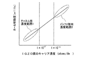
In、Ga、及びZnを含む酸化物半導体膜(IGZO膜)はキャリア濃度が高くなるにつれ、ホール移動度も高くなる特性を有している。よって、In、Ga、及びZnを含む酸化物半導体膜のキャリア濃度とホール移動度の関係は図27に示すようになる。本発明の一形態において、半導体層のチャネルとして適するIGZO膜のキャリア濃度範囲(チャネル用濃度範囲1)は1×10¹⁷atoms/cm3未満(より好ましくは1×1011atoms/cm3以上)、バッファ層として適するIGZO膜のキャリア濃度範囲(バッファ層濃度範囲2)は、1×1018atoms/cm3以上(1×1022atoms/cm3以下)が好ましい。上記IGZO膜のキャリア濃度は、半導体層として用いた場合、室温で、ソース、ドレイン、及びゲート電圧を印加しない状態での値である。 An oxide semiconductor film (IGZO film) containing In, Ga, and Zn has a characteristic that hole mobility increases as the carrier concentration increases. Therefore, the relationship between the carrier concentration and the hole mobility of the oxide semiconductor film containing In, Ga, and Zn is as shown in FIG. In one embodiment of the present invention, a carrier concentration range (channel concentration range 1) of an IGZO film suitable as a channel of a semiconductor layer is less than 1 × 10 17 atoms / cm 3 (more preferably 1 × 10 11 atoms / cm 3 or more). The carrier concentration range (buffer layer concentration range 2) of the IGZO film suitable as the buffer layer is preferably 1 × 10 18 atoms / cm 3 or more (1 × 10 22 atoms / cm 3 or less). When used as a semiconductor layer, the carrier concentration of the IGZO film is a value obtained when no source, drain, and gate voltages are applied at room temperature.
チャネル用のIGZO膜のキャリア濃度範囲が上記範囲を越えると、薄膜トランジスタとしてノーマリーオンになる恐れがある。よって本発明の一形態のキャリア濃度範囲のIGZO膜を半導体層のチャネルとして用いることで信頼性の高い薄膜トランジスタとすることができる。 When the carrier concentration range of the channel IGZO film exceeds the above range, the thin film transistor may be normally on. Therefore, a highly reliable thin film transistor can be obtained by using an IGZO film having a carrier concentration range of one embodiment of the present invention as a channel of a semiconductor layer.
また、ソース電極層及びドレイン電極層にチタン膜を用いることが好ましい。例えば、チタン膜、アルミニウム膜、チタン膜の積層を用いると低抵抗であり、かつアルミニウム膜にヒロックが発生しにくい。 In addition, a titanium film is preferably used for the source electrode layer and the drain electrode layer. For example, when a stacked film of a titanium film, an aluminum film, and a titanium film is used, the resistance is low and hillocks are hardly generated in the aluminum film.
本発明の半導体装置の作製方法の一形態は、基板上にソース電極層及びドレイン電極層を形成し、ソース電極層及びドレイン電極層上にn型の導電型を有するバッファ層を形成し、バッファ層上に半導体層を形成し、半導体層上にゲート絶縁層を形成し、ゲート絶縁層上にゲート電極層を形成し、半導体層及びバッファ層はインジウム、ガリウム、及び亜鉛を含む酸化物半導体層を用いて形成し、バッファ層のキャリア濃度は、半導体層のキャリア濃度より高く、半導体層とソース電極層及びドレイン電極層とはバッファ層を介して電気的に接続する。 In one embodiment of a method for manufacturing a semiconductor device of the present invention, a source electrode layer and a drain electrode layer are formed over a substrate, a buffer layer having n-type conductivity is formed over the source electrode layer and the drain electrode layer, and the buffer A semiconductor layer is formed over the layer, a gate insulating layer is formed over the semiconductor layer, a gate electrode layer is formed over the gate insulating layer, and the semiconductor layer and the buffer layer are oxide semiconductor layers containing indium, gallium, and zinc The carrier concentration of the buffer layer is higher than the carrier concentration of the semiconductor layer, and the semiconductor layer, the source electrode layer, and the drain electrode layer are electrically connected through the buffer layer.
半導体層、ゲート絶縁層、及びゲート電極層は大気に曝さずに連続的に形成することができる。連続して成膜すると、ごみとなる大気中の不純物が界面に混入することによる不良を軽減することができる。 The semiconductor layer, the gate insulating layer, and the gate electrode layer can be continuously formed without being exposed to the air. When the films are continuously formed, defects caused by impurities in the atmosphere that become dust can be reduced.
ソース電極層、ドレイン電極層、バッファ層、半導体層、ゲート絶縁層、及びゲート電極層はスパッタ法(スパッタリング法)で形成すればよい。ゲート絶縁層及び半導体層は酸素雰囲気下(又は酸素90%以上、希ガス(アルゴン)10%以下)で、n型の導電型を有するバッファ層は希ガス(アルゴン)雰囲気下で成膜することが好ましい。
The source electrode layer, the drain electrode layer, the buffer layer, the semiconductor layer, the gate insulating layer, and the gate electrode layer may be formed by a sputtering method (sputtering method). The gate insulating layer and the semiconductor layer are formed in an oxygen atmosphere (or
このようにスパッタ法を用いて連続的に成膜すると、生産性が高く、薄膜界面の信頼性が安定する。また、半導体層とゲート絶縁層を酸素雰囲気下で成膜し、酸素を多く含ませるようにすると、劣化による信頼性の低下や、薄膜トランジスタ特性のノーマリーオン側へのシフトなどを軽減することができる。 When the film is continuously formed by using the sputtering method as described above, the productivity is high and the reliability of the thin film interface is stabilized. In addition, when the semiconductor layer and the gate insulating layer are formed in an oxygen atmosphere and contain a large amount of oxygen, a decrease in reliability due to deterioration or a shift of the thin film transistor characteristics to the normally-on side can be reduced. it can.
本発明の一形態によって、光電流が少なく、寄生容量が小さく、オンオフ比の高い薄膜トランジスタを得ることができ、良好な動特性を有する薄膜トランジスタを作製できる。よって、電気特性が高く信頼性のよい薄膜トランジスタを有する半導体装置を提供することができる。 According to one embodiment of the present invention, a thin film transistor with low photocurrent, small parasitic capacitance, high on / off ratio, and favorable dynamic characteristics can be manufactured. Thus, a semiconductor device including a thin film transistor with high electrical characteristics and high reliability can be provided.
実施の形態について、図面を用いて詳細に説明する。但し、本発明は以下の説明に限定されず、本発明の趣旨及びその範囲から逸脱することなくその形態及び詳細を様々に変更し得ることは当業者であれば容易に理解される。従って、本発明は以下に示す実施の形態の記載内容に限定して解釈されるものではない。なお、以下に説明する本発明の構成において、同一部分又は同様な機能を有する部分には同一の符号を異なる図面間で共通して用い、その繰り返しの説明は省略する。 Embodiments will be described in detail with reference to the drawings. However, the present invention is not limited to the following description, and it is easily understood by those skilled in the art that modes and details can be variously changed without departing from the spirit and scope of the present invention. Therefore, the present invention should not be construed as being limited to the description of the embodiments below. Note that in structures of the present invention described below, the same portions or portions having similar functions are denoted by the same reference numerals in different drawings, and description thereof is not repeated.
(実施の形態1)
本実施の形態では、薄膜トランジスタ及びその作製工程について、図1乃至図4を用いて説明する。
(Embodiment 1)
In this embodiment, a thin film transistor and a manufacturing process thereof will be described with reference to FIGS.
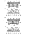
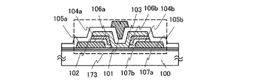
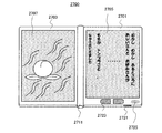
本実施の形態のトップゲート構造の順スタガ型薄膜トランジスタである薄膜トランジスタ170a、170bを図1に示す。図1(A1)は平面図であり、図1(A2)は図1(A1)における線A1−A2の断面図である。図1(B1)は平面図であり、図1(B2)は図1(B1)における線B1−B2の断面図である。
図1において、基板100上に、絶縁層107a、絶縁層107b、ソース電極層又はドレイン電極層105a、105b、n型の導電型を有するバッファ層104a、104b、半導体層103、ゲート絶縁層102、ゲート電極層101を有する薄膜トランジスタ170a、170bが設けられている。
In FIG. 1, over a
半導体層103としてIn、Ga、及びZnを含む酸化物半導体膜を用い、ソース電極層又はドレイン電極層105a、105bとIGZO半導体層である半導体層103との間に、半導体層103よりもキャリア濃度の高いバッファ層104a、104bを意図的に設けることによってオーミック性のコンタクトを形成する。
An oxide semiconductor film containing In, Ga, and Zn is used as the
バッファ層104a、104bとしては、n型の導電型を有するIn、Ga、及びZnを含む酸化物半導体膜を用いる。バッファ層104a、104bにn型を付与する不純物元素を含ませてもよい。不純物元素として、例えばマグネシウム、アルミニウム、チタン、鉄、錫、カルシウム、ゲルマニウム、スカンジウム、イットリウム、ジルコニウム、ハフニウム、ボロン、タリウム、鉛などを用いることができる。マグネシウム、アルミニウム、チタンなどをバッファ層に含ませると、酸素のブロッキング効果などがあり、成膜後の加熱処理などによって半導体層の酸素濃度を最適な範囲内に保持できる。
As the
本発明の一形態において、半導体層のキャリア濃度範囲は1×10¹⁷atoms/cm3未満(より好ましくは1×1011atoms/cm3以上)、バッファ層のキャリア濃度範囲は、1×1018atoms/cm3以上(1×1022atoms/cm3以下)が好ましい。 In one embodiment of the present invention, the carrier concentration range of the semiconductor layer is less than 1 × 10 17 atoms / cm 3 (more preferably, 1 × 10 11 atoms / cm 3 or more), and the carrier concentration range of the buffer layer is 1 × 10 18. atoms / cm 3 or more (1 × 10 22 atoms / cm 3 or less) are preferable.
チャネル用のIGZO層のキャリア濃度範囲が上記範囲を越えると、薄膜トランジスタとしてノーマリーオンになる恐れがある。よって本発明の一形態のキャリア濃度範囲のIGZO膜を半導体層のチャネルとして用いることで信頼性の高い薄膜トランジスタとすることができる。 If the carrier concentration range of the channel IGZO layer exceeds the above range, the thin film transistor may be normally on. Therefore, a highly reliable thin film transistor can be obtained by using an IGZO film having a carrier concentration range of one embodiment of the present invention as a channel of a semiconductor layer.
また半導体層とバッファ層との間に、n−層として機能するバッファ層よりキャリア濃度が低く半導体層よりキャリア濃度が高い第2のバッファ層を設ける場合は、第2のバッファ層のキャリア濃度を、半導体層とバッファ層のキャリア濃度の間の濃度範囲とすればよい。 In the case where a second buffer layer having a carrier concentration lower than that of the buffer layer functioning as an n − layer and having a carrier concentration higher than that of the semiconductor layer is provided between the semiconductor layer and the buffer layer, the carrier concentration of the second buffer layer is set to The concentration range may be between the carrier concentration of the semiconductor layer and the buffer layer.
バッファ層104a、104bは、n+層として機能し、ドレイン領域またはソース領域とも呼ぶことができる。 The buffer layers 104a and 104b function as n + layers and can also be referred to as drain regions or source regions.
図1(A1)(A2)の薄膜トランジスタ170aは、半導体層103のエッチング加工の工程で、バッファ層104a、104bも同マスクでエッチング加工した例であり、半導体層103及びゲート絶縁層102と接するバッファ層104a、104bの端部とは一致しており連続的になっている。
A
図1(B1)(B2)の薄膜トランジスタ170bは、半導体層103のエッチング加工の工程で、バッファ層104a、104bにはエッチング加工を行わない例であり、バッファ層104a、104bはソース電極層又はドレイン電極層105a、105b上に、半導体層103端部より延在して露出している。
A
薄膜トランジスタ170a、170bでは、ソース電極層又はドレイン電極層105a、105b、バッファ層104a、104b、及び半導体層103をゲート絶縁層102が覆うように設けられる例を示すが、ゲート絶縁層102を半導体層103と同じ形状にエッチング加工してもよい。
In the
本発明の一形態において半導体層103として用いる酸化物半導体層は光吸収が少ないために、半導体層のチャネル形成領域をゲート電極層で覆って光から遮光する必要がない。よって、ソース電極層及びドレイン電極層と、ゲート電極層とを、半導体層のチャネル形成領域において重ならない構造にすることができ寄生容量を軽減することができる。
In one embodiment of the present invention, an oxide semiconductor layer used as the
本発明の一形態では、半導体層103においてソース領域又はドレイン領域であるバッファ層104a、104b間に設けられる領域がチャネル形成領域となる。よってチャネル長はチャネル長方向においてソース領域となるバッファ層とドレイン領域となるバッファ層との間の長さである。半導体層103のチャネル形成領域において、ゲート電極層101と重なっていない領域であっても、ゲート電極層101の電圧印加によってチャネルは形成され、チャネル領域となる。また、ゲート電極層101の端部とバッファ層104a、104bの端部とが一致していてもよい。
In one embodiment of the present invention, a region provided between the
バッファ層104a、104bはソース電極層又はドレイン電極層105a、105bと半導体層103との間に設ける。よって、少なくともバッファ層104a、104bはソース電極層及びドレイン電極層105a、105bにおいて半導体層103と接する側(ゲート絶縁層と接する側とは反対側)の端部を覆うように設けられる。
The buffer layers 104 a and 104 b are provided between the source or drain electrode layers 105 a and 105 b and the
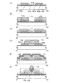
図1(A1)(A2)の薄膜トランジスタ170aの作製方法を図3(A)乃至(F)を用いて説明する。
A method for manufacturing the
本発明の一形態の順スタガ型薄膜トランジスタでは、半導体層が基板と接して設けられるので、基板からの不純物による半導体層の汚染を防止するために下地膜として絶縁膜を形成することが好ましい。下地膜としては、CVD法やスパッタ法等を用いて、酸化珪素膜、窒化珪素膜、酸化窒化珪素膜、または窒化酸化珪素膜の単層、又は積層で形成すればよい。本実施の形態では、基板100上に下地膜として機能する絶縁層107a、107bを形成する。
In the forward staggered thin film transistor of one embodiment of the present invention, since the semiconductor layer is provided in contact with the substrate, an insulating film is preferably formed as a base film in order to prevent contamination of the semiconductor layer due to impurities from the substrate. As the base film, a single layer or a stacked layer of a silicon oxide film, a silicon nitride film, a silicon oxynitride film, or a silicon nitride oxide film may be formed by a CVD method, a sputtering method, or the like. In this embodiment, insulating
基板100は、バリウムホウケイ酸ガラス、アルミノホウケイ酸ガラス、若しくはアルミノシリケートガラスなど、フュージョン法やフロート法で作製される無アルカリガラス基板、セラミック基板の他、本作製工程の処理温度に耐えうる耐熱性を有するプラスチック基板等を用いることができる。また、ステンレス合金などの金属基板の表面に絶縁膜を設けた基板を適用しても良い。基板100の大きさは、320mm×400mm、370mm×470mm、550mm×650mm、600mm×720mm、680mm×880mm、730mm×920mm、1000mm×1200mm、1100mm×1250mm、1150mm×1300mm、1500mm×1800mm、1900mm×2200mm、2160mm×2460mm、2400mm×2800mm、又は2850mm×3050mm等を用いることができる。
The
絶縁層107b上にソース電極層又はドレイン電極層105a、105bを形成し、ソース電極層又はドレイン電極層105a、105b上にn型の導電型を有する半導体膜114を形成する。半導体膜114は、n型の導電型を有するIn、Ga、及びZnを含む酸化物半導体膜であるn型の導電型を有する半導体膜である。
Source or
ソース電極層又はドレイン電極層105a、105bは、スパッタ法や真空蒸着法で絶縁層107b上に導電膜を形成し、当該導電膜上にフォトリソグラフィ技術またはインクジェット法によりマスクを形成し、当該マスクを用いて導電膜をエッチングすることで、形成することができる。
For the source or drain
ソース電極層又はドレイン電極層105a、105bは、アルミニウム、銅、又はシリコン、チタン、ネオジム、スカンジウム、モリブデンなどの耐熱性向上元素若しくはヒロック防止元素が添加されたアルミニウム合金の単層または積層で形成することが好ましい。また、n型の導電型を有する半導体膜114と接する側の膜を、チタン、タンタル、モリブデン、タングステン、またはこれらの元素の窒化物で形成し、その下にアルミニウムまたはアルミニウム合金を形成した積層構造としても良い。更には、アルミニウムまたはアルミニウム合金の上面及び下面を、チタン、タンタル、モリブデン、タングステン、またはこれらの元素の窒化物で挟んだ積層構造としてもよい。ここでは、ソース電極層又はドレイン電極層105a、105bとして、チタン膜、アルミニウム膜、及びチタン膜の積層導電膜を用いる。
The source or drain
チタン膜、アルミニウム膜、チタン膜の積層を用いると低抵抗であり、かつアルミニウム膜にヒロックが発生しにくい。 When a laminate of a titanium film, an aluminum film, and a titanium film is used, the resistance is low and hillocks are hardly generated in the aluminum film.
ソース電極層又はドレイン電極層105a、105bは、スパッタ法や真空蒸着法で形成する。また、ソース電極層又はドレイン電極層105a、105bは、銀、金、銅などの導電性ナノペーストを用いてスクリーン印刷法、インクジェット法等を用いて吐出し焼成して形成しても良い。
The source or drain
なお、ソース電極層又はドレイン電極層105a、105b上には半導体膜や配線を形成するので、段切れ防止のため端部がテーパー状になるように加工することが望ましい。
Note that since a semiconductor film or a wiring is formed over the source or drain
n型の導電型を有する半導体膜114は膜厚2〜100nm(好ましくは20〜50nm)とすればよい。n型の導電型を有する半導体膜114は希ガス(好ましくはアルゴン)雰囲気下で成膜することが好ましい。
The
例えば、n型の導電型を有する半導体膜114としては、DCマグネトロンスパッタ法を用いて形成することができる。希ガスのみの雰囲気下でパルスDCスパッタ法のスパッタリングを行い、バッファ層となるIGZO膜を形成する。このIGZO膜は、後に形成される半導体層103となる酸素過剰のIGZO膜(半導体膜111)よりも膜中の酸素濃度が低い。また、IGZO膜としては、酸素過剰のIGZO膜(半導体膜111)よりも高いキャリア濃度とすることが好ましく、ターゲットとしてIn、Ga、及びZnを含む酸化物半導体にさらにMgやAlやTiを含むターゲットを用いてもよい。MgやAlやTiは、酸化反応しやすい材料であり、これらの材料をIGZO膜に含ませると酸素のブロッキング効果などがあり、成膜後の加熱処理などを行ったとしても半導体層の酸素濃度を最適な範囲内に保持できる。このIGZO膜はソース領域またはドレイン領域として機能する。
For example, the
n型の導電型を有する半導体膜114上にマスク116を形成する。マスク116は、フォトリソグラフィ技術またはインクジェット法により形成する。n型の導電型を有する半導体膜114を、マスク116を用いてエッチングにより加工し、n型の導電型を有する半導体層115a、115bを形成する(図3(B)参照。)。
A
次に、半導体層115a、115b上に半導体膜111を形成する(図3(C)参照。)。
Next, the
半導体膜111としては、In、Ga、及びZnを含む酸化物半導体膜を形成する。例えば、半導体膜111として、スパッタ法を用いて、In、Ga、及びZnを含む酸化物半導体膜を膜厚50nmで形成すればよい。具体的な条件例としては、直径8インチのIn、Ga、及びZnを含む酸化物半導体ターゲットを用いて、基板とターゲットの間との距離を170mm、圧力0.4Pa、直流(DC)電源0.5kW、アルゴン又は酸素雰囲気下で成膜することができる。また、パルス直流(DC)電源を用いると、ごみが軽減でき、膜厚分布も均一となるために好ましい。
As the
半導体膜111やn型の導電型を有する半導体膜114などの酸化物半導体膜のスパッタ法以外の他の成膜方法としては、パルスレーザー蒸着法(PLD法)及び電子ビーム蒸着法などの気相法を用いることができる。気相法の中でも、材料系の組成を制御しやすい点では、PLD法が、量産性の点からは、上述したようにスパッタ法が適している。
As a film formation method other than the sputtering method of the oxide semiconductor film such as the
また、半導体膜111やn型の導電型を有する半導体膜114などのIGZO半導体膜のエッチングには、クエン酸やシュウ酸などの有機酸をエッチャントに用いることができる。例えば、50nmの半導体膜111はITO07N(関東化学社製)を使い150秒でエッチング加工できる。
In addition, an organic acid such as citric acid or oxalic acid can be used as an etchant for etching the IGZO semiconductor film such as the
In、Ga、及びZnを含む酸化物半導体膜である半導体膜111は酸素雰囲気下(又は酸素90%以上、希ガス(アルゴン、又はヘリウムなど)10%以下)で成膜することが好ましい。
The
次に半導体膜111及びn型の導電型を有する半導体層115a、115bを、マスク113を用いてエッチングにより加工し、半導体層103、及びバッファ層104a、104bを形成する(図3(D)参照。)。半導体層103及びバッファ層104a、104bは、フォトリソグラフィ技術または液滴吐出法によりマスク113を形成し、当該マスク113を用いて半導体膜111及びn型の導電型を有する半導体層115a、115bをエッチングすることで、形成することができる。
Next, the
図3(D)に示すように、薄膜トランジスタ170aは、半導体層103のエッチング加工の工程で、バッファ層104a、104bも同マスクでエッチング加工する。よって、半導体層103及びゲート絶縁層102と接するバッファ層104a、104bの端部とは一致しており連続的になっている。
As shown in FIG. 3D, in the
半導体層103及びバッファ層104a、104bの端部をテーパーを有する形状にエッチングすることで、半導体層103及びバッファ層104a、104bの段差形状による、上に積層される配線の段切れを防ぐことができる。
By etching the end portions of the
マスク113を除去した後、ソース電極層又はドレイン電極層105a、105b、バッファ層104a、104b、半導体層103上にゲート絶縁層102を形成し、ゲート絶縁層102上に導電膜117を形成する(図3(E)参照。)。
After the
ゲート絶縁層102は、窒化珪素膜または窒化酸化珪素膜と、酸化珪素膜または酸化窒化珪素膜との順に積層して形成することができる。なお、ゲート絶縁層を2層とせず、基板側から窒化珪素膜または窒化酸化珪素膜と、酸化珪素膜または酸化窒化珪素膜と、窒化珪素膜または窒化酸化珪素膜との順に3層積層して形成することができる。また、ゲート絶縁層を、酸化珪素膜、窒化珪素膜、酸化窒化珪素膜、または窒化酸化珪素膜の単層で形成することができる。
The
また、ゲート絶縁層102として、スパッタ法により半導体層103上に酸化珪素膜を形成し、酸化珪素膜上にプラズマCVD法により窒化珪素膜を積層してもよい。スパッタ法により酸化珪素膜を形成し、酸化珪素膜上にプラズマCVD法により窒化珪素膜と酸化珪素膜を順に積層してもよい。
Alternatively, as the
ここでは、酸化窒化珪素膜とは、その組成として、窒素よりも酸素の含有量が多いものであって、濃度範囲として酸素が55〜65原子%、窒素が1〜20原子%、Siが25〜35原子%、水素が0.1〜10原子%の範囲で含まれるものをいう。また、窒化酸化珪素膜とは、その組成として、酸素よりも窒素の含有量が多いものであって、濃度範囲として酸素が15〜30原子%、窒素が20〜35原子%、Siが25〜35原子%、水素が15〜25原子%の範囲で含まれるものをいう。 Here, the silicon oxynitride film has a composition that contains more oxygen than nitrogen and has a concentration range of 55 to 65 atomic%, 1 to 20 atomic%, and 25 Si. -35 atomic%, and hydrogen is contained in the range of 0.1-10 atomic%. The silicon nitride oxide film has a composition containing more nitrogen than oxygen, and the concentration ranges of oxygen are 15 to 30 atomic%, nitrogen is 20 to 35 atomic%, and Si is 25 to 25%. 35 atomic% and hydrogen are included in the range of 15 to 25 atomic%.
また、ゲート絶縁層102として、アルミニウム、イットリウム、又はハフニウムの酸化物、窒化物、酸化窒化物、又は窒化酸化物の一種又はそれらの化合物を少なくとも2種以上含む化合物を用いることもできる。
Alternatively, the
また、ゲート絶縁層102に、塩素、フッ素などのハロゲン元素を含ませてもよい。ゲート絶縁層102中のハロゲン元素の濃度は、濃度ピークにおいて1×10¹⁵atoms/cm3以上1×1020atoms/cm3以下とすればよい。
Further, the
また、ゲート絶縁層102は酸素雰囲気下(又は酸素90%以上、希ガス(アルゴン、又はヘリウムなど)10%以下)で成膜することが好ましい。
The
次に、導電膜117上にマスク118を形成する。マスク118を用いて導電膜117をエッチング加工して、ゲート電極層101を形成する(図3(F)参照。)。
Next, a
ゲート電極層101は、チタン、モリブデン、クロム、タンタル、タングステン、アルミニウムなどの金属材料またはその合金材料を用いて形成する。また、銀、金、銅などの導電性ナノペーストを用いてインクジェット法により吐出し焼成して、ゲート電極層101を形成することができる。なお、ゲート電極層上に、上記金属材料の窒化物膜を設けてもよい。また、ゲート電極層101は単層構造としても積層構造としてもよく、例えばゲート絶縁層102側からアルミニウム膜とモリブデン膜との積層、アルミニウムとネオジムとの合金膜とモリブデン膜との積層、アルミニウム膜とチタン膜との積層、チタン膜、アルミニウム膜及びチタン膜との積層などを用いることができる。
The
この後、マスク118を除去する。以上の工程により、薄膜トランジスタ170aを形成することができる。
Thereafter, the
次に図1(B1)(B2)に示す薄膜トランジスタ170bの作製工程を図4に示す。
Next, a manufacturing process of the
図4(A)は図3(A)の工程と対応しており、絶縁層107a、107bが設けられた基板100上に、ソース電極層又はドレイン電極層105a、105b、n型の導電型を有する半導体膜114が形成されている。
4A corresponds to the step of FIG. 3A, and the source or drain
n型の導電型を有する半導体膜114上にマスク121を形成し、マスク121を用いて、n型の導電型を有する半導体膜114をエッチング加工して、バッファ層104a、104bを形成する(図4(B)参照。)。
A
絶縁層107b、バッファ層104a、104b上に半導体膜を形成し、マスク113を用いて該半導体膜をエッチング加工して半導体層103を形成する(図4(C)参照。)。図4(C)では、半導体層103を形成するエッチング工程を、バッファ層104a、104bがエッチングされない条件で行う。よって、バッファ層104a、104bはソース電極層又はドレイン電極層105a、105b上に、半導体層103端部より延在して露出する。
A semiconductor film is formed over the insulating
マスク113を除去した後、ソース電極層又はドレイン電極層105a、105b、バッファ層104a、104b、半導体層103上にゲート絶縁層102を形成し、ゲート絶縁層102上にゲート電極層101を導電膜をマスク118によってエッチング加工して形成する。
After the
この後、マスク118を除去する。以上の工程により、薄膜トランジスタ170bを形成することができる。
Thereafter, the
また、本発明の一形態において、半導体層、ゲート絶縁層、及びゲート電極層は大気に曝さずに連続的に形成することができる。連続して成膜すると、大気成分や大気中に浮遊する汚染不純物元素に汚染されることなく各積層界面を形成することができる。半導体層、ゲート絶縁層、及びゲート電極層を連続して成膜する例を図2(A)(B)に示す。 In one embodiment of the present invention, the semiconductor layer, the gate insulating layer, and the gate electrode layer can be continuously formed without being exposed to the air. When the films are continuously formed, each stacked interface can be formed without being contaminated by atmospheric components or contaminating impurity elements floating in the atmosphere. An example in which a semiconductor layer, a gate insulating layer, and a gate electrode layer are successively formed is shown in FIGS.
図2(A)は、図3(B)において、マスク116を除去した後の工程である。その後のエッチング加工において半導体層103となる半導体膜131、ゲート絶縁層132、ゲート電極層101となる導電膜133を大気に曝さずに連続成膜する(図2(B)参照。)。半導体膜131、ゲート絶縁層132、及び導電膜133はスパッタ法によって形成することが好ましい。
FIG. 2A shows a process after the
アクティブマトリクス型の表示装置においては、回路を構成する薄膜トランジスタの電気特性が重要であり、この電気特性が表示装置の性能を左右する。特に、薄膜トランジスタの電気特性のうち、しきい値電圧(Vth)が重要である。nチャネル型の薄膜トランジスタの場合、電界効果移動度が高くともしきい値電圧値が高い、或いはしきい値電圧値がマイナスであると、回路として制御することが困難である。しきい値電圧値が高く、しきい値電圧の絶対値が大きい薄膜トランジスタの場合には、駆動電圧が低い状態では薄膜トランジスタとしてのスイッチング機能を果たすことができず、負荷となる恐れがある。また、nチャネル型の薄膜トランジスタの場合、しきい値電圧値がマイナスであると、ゲート電圧が0Vでもソース電極とドレイン電極の間に電流が流れる、所謂ノーマリーオンとなりやすい。 In an active matrix display device, the electrical characteristics of the thin film transistors constituting the circuit are important, and the electrical characteristics affect the performance of the display device. In particular, the threshold voltage (Vth) is important among the electrical characteristics of thin film transistors. In the case of an n-channel thin film transistor, if the threshold voltage value is high or the threshold voltage value is negative even if the field effect mobility is high, it is difficult to control the circuit. In the case of a thin film transistor having a high threshold voltage value and a large absolute value of the threshold voltage, the switching function as the thin film transistor cannot be achieved in a state where the drive voltage is low, which may cause a load. In the case of an n-channel thin film transistor, if the threshold voltage value is negative, a so-called normally-on state in which a current flows between the source electrode and the drain electrode even when the gate voltage is 0 V is likely to occur.
nチャネル型の薄膜トランジスタの場合、ゲート電圧に正の電圧を印加してはじめてチャネルが形成されて、ドレイン電流が流れ出すトランジスタが望ましい。駆動電圧を高くしないとチャネルが形成されないトランジスタや、負の電圧状態でもチャネルが形成されてドレイン電流が流れるトランジスタは、回路に用いる薄膜トランジスタとしては不向きである。 In the case of an n-channel thin film transistor, a transistor in which a channel is formed and drain current flows only after a positive voltage is applied to the gate voltage is desirable. A transistor in which a channel is not formed unless the driving voltage is increased or a transistor in which a channel is formed and a drain current flows even in a negative voltage state is not suitable as a thin film transistor used in a circuit.
よって、In、Ga、及びZnを含む酸化物半導体膜を用いる薄膜トランジスタのゲート電圧が0Vにできるだけ近い正のしきい値電圧でチャネルが形成されることが望ましい。 Therefore, it is desirable that a channel be formed with a positive threshold voltage where the gate voltage of a thin film transistor using an oxide semiconductor film containing In, Ga, and Zn is as close to 0 V as possible.
薄膜トランジスタのしきい値電圧値は、酸化物半導体層の界面、即ち、酸化物半導体層とゲート絶縁層の界面に大きく影響すると考えられる。 The threshold voltage value of the thin film transistor is considered to greatly influence the interface between the oxide semiconductor layer, that is, the interface between the oxide semiconductor layer and the gate insulating layer.
そこで、これらの界面を清浄な状態で形成することによって、薄膜トランジスタの電気特性を向上させるとともに、製造工程の複雑化を防ぐことができ、量産性と高性能の両方を備えた薄膜トランジスタを実現する。 Therefore, by forming these interfaces in a clean state, the electrical characteristics of the thin film transistor can be improved and the manufacturing process can be prevented from becoming complicated, and a thin film transistor having both mass productivity and high performance is realized.
特に酸化物半導体層とゲート絶縁層との界面に大気中の水分が存在すると、薄膜トランジスタの電気的特性の劣化、しきい値電圧のばらつき、ノーマリーオンになりやすいといった問題を招く。酸化物半導体層とゲート絶縁層とを連続成膜することで、このような水素化合物を排除することができる。 In particular, when moisture in the air exists at the interface between the oxide semiconductor layer and the gate insulating layer, problems such as deterioration of electrical characteristics of the thin film transistor, variation in threshold voltage, and normally on are likely to occur. Such a hydrogen compound can be eliminated by continuously forming the oxide semiconductor layer and the gate insulating layer.
よって、大気に曝すことなく半導体膜131と、ゲート絶縁層132をスパッタ法により、減圧下で連続成膜することで良好な界面を有し、リーク電流が低く、且つ、電流駆動能力の高い薄膜トランジスタを実現することができる。
Therefore, a thin film transistor having a good interface, a low leakage current, and a high current driving capability by continuously forming the
このようにスパッタ法を用いて連続的に成膜すると、生産性が高く、薄膜界面の信頼性が安定する。また半導体層とゲート絶縁層を酸素雰囲気下で成膜し、酸素を多く含ませるようにすると、劣化による信頼性の低下や、薄膜トランジスタがノーマリーオンとなることを軽減することができる。 When the film is continuously formed by using the sputtering method as described above, the productivity is high and the reliability of the thin film interface is stabilized. In addition, when the semiconductor layer and the gate insulating layer are formed in an oxygen atmosphere so as to contain a large amount of oxygen, reduction in reliability due to deterioration and reduction in the thickness of the thin film transistor can be reduced.
また、半導体層とゲート電極層とを形成するエッチングに用いるマスクを、多階調マスク(代表例としては、グレートーンマスク、ハーフトーンマスク)による露光を行って形成してもよい。 Alternatively, a mask used for etching for forming the semiconductor layer and the gate electrode layer may be formed by exposure with a multi-tone mask (typically, a gray-tone mask or a half-tone mask).
多階調マスクとは、露光部分、中間露光部分、及び未露光部分に3つの露光レベルを行うことが可能なマスクであり、一度の露光及び現像工程により、複数(代表的には二種類)の厚さの領域を有するレジストマスクを形成することが可能である。このため、多階調マスクを用いることで、フォトマスクの枚数を削減することが可能である。マスク数を減らすことができるため、工程簡略化、低コスト化が計れる。 A multi-tone mask is a mask capable of performing three exposure levels on an exposed portion, an intermediate exposed portion, and an unexposed portion, and a plurality of (typically two types) can be obtained by one exposure and development process. It is possible to form a resist mask having a region with a thickness of. Therefore, the number of photomasks can be reduced by using a multi-tone mask. Since the number of masks can be reduced, the process can be simplified and the cost can be reduced.
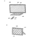
薄膜トランジスタ170a、170b上に保護膜として絶縁膜を形成してもよい。保護膜としてはゲート絶縁層と同様に形成することができる。なお、保護膜は、大気中に浮遊する有機物や金属、水蒸気などの汚染不純物の侵入を防ぐためのものであり、緻密な膜が好ましい。例えば、薄膜トランジスタ170a、170b上に保護膜として酸化珪素膜と窒化珪素膜との積層を形成すればよい。
An insulating film may be formed as a protective film over the
また、半導体層103、及びバッファ層104a、104bなどの酸化物半導体膜は成膜後に加熱処理を行うことが好ましい。加熱処理は成膜後であればどの工程で行ってもよいが、成膜直後、導電膜117の形成後、保護膜の形成後などで行うことができる。また、他の加熱処理と兼ねて行ってもよい。また加熱温度は300℃以上400℃以下、好ましくは350℃とすればよい。加熱処理は半導体層103とバッファ層104a、104bと別工程で複数回行ってもよい。
The oxide semiconductor films such as the
バッファ層(In、Ga、及びZnを含みn型の導電型を有する酸化物半導体層)を設けない、ソース電極層及びドレイン電極層、半導体層(In、Ga、及びZnを含む酸化物半導体層)、ゲート絶縁層、ゲート電極層という積層構造であると、ゲート電極層とソース電極層又はドレイン電極層との距離が近くなり、間に生じる寄生容量が増加してしまう。さらに、この寄生容量の増加は、半導体層の薄膜化によってより顕著になる。本実施の形態では、In、Ga、及びZnを含むn型の導電型を有する酸化物半導体層というようなキャリア濃度が高いバッファ層を設ける、ソース電極層及びドレイン電極層、バッファ層、半導体層、ゲート絶縁層、ゲート電極層という積層構造を有する薄膜トランジスタとしているため、半導体層の膜厚が薄膜であっても寄生容量を抑制することができる。 A source electrode layer, a drain electrode layer, and a semiconductor layer (an oxide semiconductor layer including In, Ga, and Zn) without providing a buffer layer (an oxide semiconductor layer including In, Ga, and Zn and having an n-type conductivity type) ) In the case of a stacked structure of a gate insulating layer and a gate electrode layer, the distance between the gate electrode layer and the source electrode layer or the drain electrode layer becomes short, and the parasitic capacitance generated therebetween increases. Furthermore, this increase in parasitic capacitance becomes more conspicuous as the semiconductor layer becomes thinner. In this embodiment, a source electrode layer, a drain electrode layer, a buffer layer, and a semiconductor layer in which a buffer layer having a high carrier concentration such as an oxide semiconductor layer having n-type conductivity including In, Ga, and Zn is provided. Since the thin film transistor has a stacked structure of a gate insulating layer and a gate electrode layer, parasitic capacitance can be suppressed even when the semiconductor layer is thin.
本実施の形態によって、光電流が少なく、寄生容量が小さく、オンオフ比の高い薄膜トランジスタを得ることができ、良好な動特性を有する薄膜トランジスタを作製できる。よって、電気特性が高く信頼性のよい薄膜トランジスタを有する半導体装置を提供することができる。 According to this embodiment, a thin film transistor with low photocurrent, small parasitic capacitance, and high on / off ratio can be obtained, and a thin film transistor having favorable dynamic characteristics can be manufactured. Thus, a semiconductor device including a thin film transistor with high electrical characteristics and high reliability can be provided.
(実施の形態2)
本実施の形態は、マルチゲート構造の薄膜トランジスタの例である。従って、他は実施の形態1と同様に行うことができ、実施の形態1と同一部分又は同様な機能を有する部分、及び工程の繰り返しの説明は省略する。
(Embodiment 2)
This embodiment is an example of a thin film transistor having a multi-gate structure. Accordingly, the other steps can be performed in the same manner as in
本実施の形態では、半導体装置に用いられる薄膜トランジスタについて、図5(A1)(A2)(B1)(B2)を用いて説明する。図5(A1)は平面図であり、図5(A2)は図5(A1)における線E1−E2の断面図である。図5(B1)は平面図であり、図5(B2)は図5(B1)における線F1−F2の断面図である。 In this embodiment, a thin film transistor used for a semiconductor device will be described with reference to FIGS. 5A1 to 5A2 and 5B1 and 5B2. 5A1 is a plan view, and FIG. 5A2 is a cross-sectional view taken along line E1-E2 in FIG. 5A1. 5B1 is a plan view, and FIG. 5B2 is a cross-sectional view taken along line F1-F2 in FIG. 5B1.
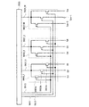
図5(A1)(A2)に示すように、基板150上に、絶縁層157a、157b、ソース電極層又はドレイン電極層155a、155b、配線層156、半導体層153、バッファ層154a、154b、154c、ゲート電極層151a、151bを含むマルチゲート構造の薄膜トランジスタ171aが設けられている。薄膜トランジスタ171aにおいては、半導体層153はゲート絶縁層152を介して、ゲート電極層151a、151bの下に跨って連続して設けられる。
As shown in FIGS. 5A1 and 5A2, insulating
図5(B1)(B2)は他の構成のマルチゲート構造の薄膜トランジスタ171bを示す。図5(B1)(B2)に示すように、基板150上に、絶縁層157a、157b、ソース電極層又はドレイン電極層155a、155b、配線層156、半導体層153a、153b、バッファ層154a、154b、154c、154d、ゲート電極層151a、151bを含むマルチゲート構造の薄膜トランジスタ171bが設けられている。
5B1 and 5B2 illustrate a multi-gate
薄膜トランジスタ171bでは、配線層156上において、半導体層が半導体層153a、153bに、バッファ層が154c、154dに分断されている。半導体層153aと半導体層153bとは、一方をバッファ層154c、バッファ層154d及び配線層156を介して電気的に接続しており、他方でそれぞれ半導体層153aはバッファ層154aを介してソース電極層又はドレイン電極層155aと、半導体層153bはバッファ層154bを介してソース電極層又はドレイン電極層155bと電気的に接続している。
In the
半導体層153(153a、153b)は、In、Ga、及びZnを含む酸化物半導体層であり、バッファ層154a、154b、154c、154dはn型の導電型を有するIn、Ga、及びZnを含む酸化物半導体層である。バッファ層154a、154b、154c、154dは、半導体層153(153a、153b)よりキャリア濃度が高い。
The semiconductor layer 153 (153a, 153b) is an oxide semiconductor layer containing In, Ga, and Zn, and the
このように、本発明の一形態のマルチゲート構造の薄膜トランジスタにおいては、各ゲート電極層下に形成される半導体層は連続して設けられてもよいし、バッファ層及び配線層などを介して複数の半導体層が電気的に接続して設けられてもよい。 As described above, in the multi-gate thin film transistor of one embodiment of the present invention, a semiconductor layer formed under each gate electrode layer may be provided continuously, or a plurality of layers may be provided via a buffer layer, a wiring layer, or the like. These semiconductor layers may be provided in an electrically connected state.
本発明の一形態のマルチゲート構造の薄膜トランジスタは、オフ電流が少なく、そのような薄膜トランジスタを含む半導体装置は高い電気特性及び高信頼性を付与することができる。 A multi-gate thin film transistor of one embodiment of the present invention has low off-state current, and a semiconductor device including such a thin film transistor can have high electrical characteristics and high reliability.
本実施の形態では、マルチゲート構造としてゲート電極層が2つのダブルゲート構造の例を示すが、より多くのゲート電極層を有するトリプルゲート構造などにも適用することができる。 In this embodiment mode, an example of a double gate structure having two gate electrode layers as a multi-gate structure is shown; however, the present invention can also be applied to a triple gate structure having more gate electrode layers.
本実施の形態は他の実施の形態と適宜組み合わせて実施することができる。 This embodiment can be implemented in appropriate combination with any of the other embodiments.
(実施の形態3)
本実施の形態は、薄膜トランジスタにおいてバッファ層を積層する例である。従って、他は実施の形態1又は実施の形態2と同様に行うことができ、実施の形態1又は実施の形態2と同一部分又は同様な機能を有する部分、及び工程の繰り返しの説明は省略する。
(Embodiment 3)
This embodiment is an example in which a buffer layer is stacked in a thin film transistor. Therefore, the other steps can be performed in the same manner as in
本実施の形態では、半導体装置に用いられる薄膜トランジスタ173について、図6を用いて説明する。
In this embodiment, a
図6に示すように、基板100上に、絶縁層107a、107b、ソース電極層又はドレイン電極層105a、105b、バッファ層104a、104b、バッファ層106a、106b、半導体層103、ゲート絶縁層102、ゲート電極層101を含む薄膜トランジスタ173が設けられている。
As shown in FIG. 6, insulating
本実施の形態の薄膜トランジスタ173は、半導体層103とバッファ層104a、104bとの間にそれぞれ第2のバッファ層としてバッファ層106a、106bが設けられている。
In the
半導体層103は、In、Ga、及びZnを含む酸化物半導体層であり、バッファ層104a、104b、バッファ層106a、106bはn型の導電型を有するIn、Ga、及びZnを含む酸化物半導体層である。
The
半導体層103とバッファ層104a、104bとの間に設けられる第2のバッファ層(バッファ層106a、106b)は、キャリア濃度が半導体層103より高く、バッファ層104a、104bより低い。バッファ層104a、104bがn+層として機能するのに対して、第2のバッファ層(バッファ層106a、106b)はn−層として機能する。
The second buffer layer (
本発明の一形態において、半導体層103として適するキャリア濃度範囲は1×10¹⁷atoms/cm3未満(より好ましくは1×1011atoms/cm3以上)、バッファ層として適するキャリア濃度範囲は、1×1018atoms/cm3以上(1×1022atoms/cm3以下)が好ましい。
In one embodiment of the present invention, a carrier concentration range suitable for the
チャネル用の半導体層103キャリア濃度範囲が上記範囲を越えると、薄膜トランジスタとしてノーマリーオンになる恐れがある。よって本発明の一形態のキャリア濃度範囲のIGZO膜を半導体層103のチャネルとして用いることで信頼性の高い薄膜トランジスタとすることができる。
If the carrier concentration range of the
n−層として機能するバッファ層106a、106bとして適する濃度範囲は、n+層として機能するバッファ層104a、104bよりキャリア濃度が低く半導体層103よりキャリア濃度が高い濃度範囲とすればよい。
A concentration range suitable for the
このように、半導体層とソース電極層又はドレイン電極層との間に設けられるバッファ層は積層構造としてもよく、そのキャリア濃度は半導体層からソース電極層又はドレイン電極層へ向かって高くなるように制御する。 As described above, the buffer layer provided between the semiconductor layer and the source or drain electrode layer may have a stacked structure, and the carrier concentration thereof increases from the semiconductor layer toward the source or drain electrode layer. Control.
本発明の一形態の積層バッファ層を有する薄膜トランジスタは、オフ電流が少なく、そのような薄膜トランジスタを含む半導体装置は高い電気特性及び高信頼性を付与することができる。また、半導体層103からソース電極層又はドレイン電極層に向かってキャリア濃度が上昇するように勾配をつけることにより、半導体層103とソース電極層又はドレイン電極層との間の接触抵抗を低減することができる。また、第2のバッファ層を設けることにより半導体層103との接合界面に集中する電界をより緩和することができる。
A thin film transistor including the stacked buffer layer of one embodiment of the present invention has low off-state current, and a semiconductor device including such a thin film transistor can have high electrical characteristics and high reliability. In addition, the contact resistance between the
本実施の形態は他の実施の形態と適宜組み合わせて実施することができる。 This embodiment can be implemented in appropriate combination with any of the other embodiments.
(実施の形態4)
本実施の形態では、半導体装置の一例である表示装置において、同一基板上に少なくとも駆動回路の一部と、画素部に配置する薄膜トランジスタを作製する例について以下に説明する。
(Embodiment 4)
In this embodiment, an example in which at least part of a driver circuit and a thin film transistor placed in a pixel portion are formed over the same substrate in a display device which is an example of a semiconductor device will be described below.
画素部に配置する薄膜トランジスタは、実施の形態1乃至実施の形態3のいずれか一に従って形成する。また、実施の形態1乃至実施の形態3のいずれか一に示す薄膜トランジスタはnチャネル型TFTであるため、駆動回路のうち、nチャネル型TFTで構成することができる駆動回路の一部を画素部の薄膜トランジスタと同一基板上に形成する。
The thin film transistor disposed in the pixel portion is formed according to any one of
半導体装置の一例であるアクティブマトリクス型液晶表示装置のブロック図の一例を図12(A)に示す。図12(A)に示す表示装置は、基板5300上に表示素子を備えた画素を複数有する画素部5301と、各画素を選択する走査線駆動回路5302と、選択された画素へのビデオ信号の入力を制御する信号線駆動回路5303とを有する。
FIG. 12A illustrates an example of a block diagram of an active matrix liquid crystal display device which is an example of a semiconductor device. A display device illustrated in FIG. 12A includes a pixel portion 5301 having a plurality of pixels each provided with a display element over a
画素部5301は、信号線駆動回路5303から列方向に伸張して配置された複数の信号線S1〜Sm(図示せず。)により信号線駆動回路5303と接続され、走査線駆動回路5302から行方向に伸張して配置された複数の走査線G1〜Gn(図示せず。)により走査線駆動回路5302と接続され、信号線S1〜Sm並びに走査線G1〜Gnに対応してマトリクス状に配置された複数の画素(図示せず。)を有する。そして、各画素は、信号線Sj(信号線S1〜Smのうちいずれか一)、走査線Gi(走査線G1〜Gnのうちいずれか一)と接続される。
The pixel portion 5301 is connected to the signal line driver circuit 5303 by a plurality of signal lines S1 to Sm (not shown) arranged extending from the signal line driver circuit 5303 in the column direction. A plurality of scanning lines G1 to Gn (not shown) arranged in the direction are connected to the scanning
また、実施の形態1乃至実施の形態3のいずれか一に示す薄膜トランジスタは、nチャネル型TFTであり、nチャネル型TFTで構成する信号線駆動回路について図13を用いて説明する。
The thin film transistor described in any one of
図13に示す信号線駆動回路は、ドライバIC5601、スイッチ群5602_1〜5602_M、第1の配線5611、第2の配線5612、第3の配線5613及び配線5621_1〜5621_Mを有する。スイッチ群5602_1〜5602_Mそれぞれは、第1の薄膜トランジスタ5603a、第2の薄膜トランジスタ5603b及び第3の薄膜トランジスタ5603cを有する。
A signal line driver circuit illustrated in FIG. 13 includes a
ドライバIC5601は第1の配線5611、第2の配線5612、第3の配線5613及び配線5621_1〜5621_Mに接続される。そして、スイッチ群5602_1〜5602_Mそれぞれは、第1の配線5611、第2の配線5612、第3の配線5613及びスイッチ群5602_1〜5602_Mそれぞれに対応した配線5621_1〜5621_Mに接続される。そして、配線5621_1〜5621_Mそれぞれは、第1の薄膜トランジスタ5603a、第2の薄膜トランジスタ5603b及び第3の薄膜トランジスタ5603cを介して、3つの信号線に接続される。例えば、J列目の配線5621_J(配線5621_1〜配線5621_Mのうちいずれか一)は、スイッチ群5602_Jが有する第1の薄膜トランジスタ5603a、第2の薄膜トランジスタ5603b及び第3の薄膜トランジスタ5603cを介して、信号線Sj−1、信号線Sj、信号線Sj+1に接続される。
The
なお、第1の配線5611、第2の配線5612、第3の配線5613には、それぞれ信号が入力される。
Note that a signal is input to each of the
なお、ドライバIC5601は、単結晶基板上に形成されていることが望ましい。さらに、スイッチ群5602_1〜5602_Mは、画素部と同一基板上に形成されていることが望ましい。したがって、ドライバIC5601とスイッチ群5602_1〜5602_MとはFPCなどを介して接続するとよい。
Note that the
次に、図13に示した信号線駆動回路の動作について、図14のタイミングチャートを参照して説明する。なお、図14のタイミングチャートは、i行目の走査線Giが選択されている場合のタイミングチャートを示している。さらに、i行目の走査線Giの選択期間は、第1のサブ選択期間T1、第2のサブ選択期間T2及び第3のサブ選択期間T3に分割されている。さらに、図13の信号線駆動回路は、他の行の走査線が選択されている場合でも図14と同様の動作をする。 Next, operation of the signal line driver circuit illustrated in FIG. 13 is described with reference to a timing chart in FIG. Note that the timing chart of FIG. 14 is a timing chart when the i-th scanning line Gi is selected. Further, the selection period of the i-th scanning line Gi is divided into a first sub-selection period T1, a second sub-selection period T2, and a third sub-selection period T3. Further, the signal line driver circuit in FIG. 13 operates in the same manner as in FIG. 14 even when a scan line in another row is selected.
なお、図14のタイミングチャートは、J列目の配線5621_Jが第1の薄膜トランジスタ5603a、第2の薄膜トランジスタ5603b及び第3の薄膜トランジスタ5603cを介して、信号線Sj−1、信号線Sj、信号線Sj+1に接続される場合について示している。
Note that in the timing chart in FIG. 14, the wiring 5621_J in the J-th column is connected to the signal line Sj-1, the signal line Sj, and the signal line Sj + 1 through the first
なお、図14のタイミングチャートは、i行目の走査線Giが選択されるタイミング、第1の薄膜トランジスタ5603aのオン・オフのタイミング5703a、第2の薄膜トランジスタ5603bのオン・オフのタイミング5703b、第3の薄膜トランジスタ5603cのオン・オフのタイミング5703c及びJ列目の配線5621_Jに入力される信号5721_Jを示している。
Note that the timing chart in FIG. 14 shows the timing at which the i-th scanning line Gi is selected, the on / off timing 5703a of the first
なお、配線5621_1〜配線5621_Mには第1のサブ選択期間T1、第2のサブ選択期間T2及び第3のサブ選択期間T3において、それぞれ別のビデオ信号が入力される。例えば、第1のサブ選択期間T1において配線5621_Jに入力されるビデオ信号は信号線Sj−1に入力され、第2のサブ選択期間T2において配線5621_Jに入力されるビデオ信号は信号線Sjに入力され、第3のサブ選択期間T3において配線5621_Jに入力されるビデオ信号は信号線Sj+1に入力される。さらに、第1のサブ選択期間T1、第2のサブ選択期間T2及び第3のサブ選択期間T3において、配線5621_Jに入力されるビデオ信号をそれぞれData_j−1、Data_j、Data_j+1とする。
Note that different video signals are input to the wirings 5621_1 to 5621_M in the first sub-selection period T1, the second sub-selection period T2, and the third sub-selection period T3. For example, a video signal input to the wiring 5621_J in the first sub-selection period T1 is input to the signal line Sj-1, and a video signal input to the wiring 5621_J in the second sub-selection period T2 is input to the signal line Sj. Then, the video signal input to the wiring 5621_J in the third sub-selection period T3 is input to the signal
図14に示すように、第1のサブ選択期間T1において第1の薄膜トランジスタ5603aがオンし、第2の薄膜トランジスタ5603b及び第3の薄膜トランジスタ5603cがオフする。このとき、配線5621_Jに入力されるData_j−1が、第1の薄膜トランジスタ5603aを介して信号線Sj−1に入力される。第2のサブ選択期間T2では、第2の薄膜トランジスタ5603bがオンし、第1の薄膜トランジスタ5603a及び第3の薄膜トランジスタ5603cがオフする。このとき、配線5621_Jに入力されるData_jが、第2の薄膜トランジスタ5603bを介して信号線Sjに入力される。第3のサブ選択期間T3では、第3の薄膜トランジスタ5603cがオンし、第1の薄膜トランジスタ5603a及び第2の薄膜トランジスタ5603bがオフする。このとき、配線5621_Jに入力されるData_j+1が、第3の薄膜トランジスタ5603cを介して信号線Sj+1に入力される。
As shown in FIG. 14, in the first sub-selection period T1, the first
以上のことから、図13の信号線駆動回路は、1ゲート選択期間を3つに分割することで、1ゲート選択期間中に1つの配線5621から3つの信号線にビデオ信号を入力することができる。したがって、図13の信号線駆動回路は、ドライバIC5601が形成される基板と、画素部が形成されている基板との接続数を信号線の数に比べて約1/3にすることができる。接続数が約1/3になることによって、図13の信号線駆動回路は、信頼性、歩留まりなどを向上できる。
From the above, the signal line driver circuit in FIG. 13 can input a video signal from one
なお、図13のように、1ゲート選択期間を複数のサブ選択期間に分割し、複数のサブ選択期間それぞれにおいて、ある1つの配線から複数の信号線それぞれにビデオ信号を入力することができれば、薄膜トランジスタの配置や数、駆動方法などは限定されない。 As shown in FIG. 13, if one gate selection period is divided into a plurality of sub-selection periods and a video signal can be input from a certain wiring to each of a plurality of signal lines in each of the plurality of sub-selection periods, The arrangement and number of thin film transistors and the driving method are not limited.
例えば、3つ以上のサブ選択期間それぞれにおいて1つの配線から3つ以上の信号線それぞれにビデオ信号を入力する場合は、薄膜トランジスタ及び薄膜トランジスタを制御するための配線を追加すればよい。ただし、1ゲート選択期間を4つ以上のサブ選択期間に分割すると、1つのサブ選択期間が短くなる。したがって、1ゲート選択期間は、2つ又は3つのサブ選択期間に分割されることが望ましい。 For example, when video signals are input from one wiring to each of three or more signal lines in each of three or more sub-selection periods, a thin film transistor and a wiring for controlling the thin film transistor may be added. However, if one gate selection period is divided into four or more sub selection periods, one sub selection period is shortened. Therefore, it is desirable that one gate selection period is divided into two or three sub selection periods.
別の例として、図15のタイミングチャートに示すように、1つの選択期間をプリチャージ期間Tp、第1のサブ選択期間T1、第2のサブ選択期間T2、第3の選択期間T3に分割してもよい。さらに、図15のタイミングチャートは、i行目の走査線Giが選択されるタイミング、第1の薄膜トランジスタ5603aのオン・オフのタイミング5803a、第2の薄膜トランジスタ5603bのオン・オフのタイミング5803b、第3の薄膜トランジスタ5603cのオン・オフのタイミング5803c及びJ列目の配線5621_Jに入力される信号5821_Jを示している。図15に示すように、プリチャージ期間Tpにおいて第1の薄膜トランジスタ5603a、第2の薄膜トランジスタ5603b及び第3の薄膜トランジスタ5603cがオンする。このとき、配線5621_Jに入力されるプリチャージ電圧Vpが第1の薄膜トランジスタ5603a、第2の薄膜トランジスタ5603b及び第3の薄膜トランジスタ5603cを介してそれぞれ信号線Sj−1、信号線Sj、信号線Sj+1に入力される。第1のサブ選択期間T1において第1の薄膜トランジスタ5603aがオンし、第2の薄膜トランジスタ5603b及び第3の薄膜トランジスタ5603cがオフする。このとき、配線5621_Jに入力されるData_j−1が、第1の薄膜トランジスタ5603aを介して信号線Sj−1に入力される。第2のサブ選択期間T2では、第2の薄膜トランジスタ5603bがオンし、第1の薄膜トランジスタ5603a及び第3の薄膜トランジスタ5603cがオフする。このとき、配線5621_Jに入力されるData_jが、第2の薄膜トランジスタ5603bを介して信号線Sjに入力される。第3のサブ選択期間T3では、第3の薄膜トランジスタ5603cがオンし、第1の薄膜トランジスタ5603a及び第2の薄膜トランジスタ5603bがオフする。このとき、配線5621_Jに入力されるData_j+1が、第3の薄膜トランジスタ5603cを介して信号線Sj+1に入力される。
As another example, as shown in the timing chart of FIG. 15, one selection period is divided into a precharge period Tp, a first sub-selection period T1, a second sub-selection period T2, and a third selection period T3. May be. Further, in the timing chart of FIG. 15, the timing at which the i-th scanning line Gi is selected, the on / off timing 5803a of the first
以上のことから、図15のタイミングチャートを適用した図13の信号線駆動回路は、サブ選択期間の前にプリチャージ選択期間を設けることによって、信号線をプリチャージできるため、画素へのビデオ信号の書き込みを高速に行うことができる。なお、図15において、図14と同様なものに関しては共通の符号を用いて示し、同一部分又は同様な機能を有する部分の詳細な説明は省略する。 From the above, the signal line driver circuit in FIG. 13 to which the timing chart in FIG. 15 is applied can precharge the signal line by providing the precharge selection period before the sub selection period. Can be written at high speed. 15, components similar to those in FIG. 14 are denoted by common reference numerals, and detailed description of the same portions or portions having similar functions is omitted.
また、走査線駆動回路の構成について説明する。走査線駆動回路は、シフトレジスタ、バッファを有している。また場合によってはレベルシフタを有していても良い。走査線駆動回路において、シフトレジスタにクロック信号(CLK)及びスタートパルス信号(SP)が入力されることによって、選択信号が生成される。生成された選択信号はバッファにおいて緩衝増幅され、対応する走査線に供給される。走査線には、1ライン分の画素のトランジスタのゲート電極が接続されている。そして、1ライン分の画素のトランジスタを一斉にONにしなくてはならないので、バッファは大きな電流を流すことが可能なものが用いられる。 A structure of the scan line driver circuit will be described. The scan line driver circuit includes a shift register and a buffer. In some cases, a level shifter may be provided. In the scan line driver circuit, when a clock signal (CLK) and a start pulse signal (SP) are input to the shift register, a selection signal is generated. The generated selection signal is buffered and amplified in the buffer and supplied to the corresponding scanning line. A gate electrode of a transistor of a pixel for one line is connected to the scanning line. Since the transistors of pixels for one line must be turned on all at once, a buffer that can flow a large current is used.
走査線駆動回路の一部に用いるシフトレジスタの一形態について図16及び図17を用いて説明する。 One mode of a shift register used for part of the scan line driver circuit is described with reference to FIGS.
図16にシフトレジスタの回路構成を示す。図16に示すシフトレジスタは、複数のフリップフロップ5701_i(フリップフロップ5701_1〜5701_nのうちいずれか一)で構成される。また、第1のクロック信号、第2のクロック信号、スタートパルス信号、リセット信号が入力されて動作する。 FIG. 16 shows a circuit configuration of the shift register. The shift register illustrated in FIG. 16 includes a plurality of flip-flops 5701_i (any one of the flip-flops 5701_1 to 5701_n). In addition, the first clock signal, the second clock signal, the start pulse signal, and the reset signal are input to operate.
図16のシフトレジスタの接続関係について説明する。図16のシフトレジスタは、i段目のフリップフロップ5701_i(フリップフロップ5701_1〜5701_n)は、図17に示した第1の配線5501が第7の配線5717_i−1に接続され、図17に示した第2の配線5502が第7の配線5717_i+1に接続され、図17に示した第3の配線5503が第7の配線5717_iに接続され、図17に示した第6の配線5506が第5の配線5715に接続される。
Connection relations of the shift register in FIG. 16 are described. In the shift register in FIG. 16, the i-th flip-flop 5701_i (flip-flops 5701_1 to 5701_n) has the
また、図17に示した第4の配線5504が奇数段目のフリップフロップでは第2の配線5712に接続され、偶数段目のフリップフロップでは第3の配線5713に接続され、図17に示した第5の配線5505が第4の配線5714に接続される。
In addition, the
ただし、1段目のフリップフロップ5701_1の図17に示す第1の配線5501は第1の配線5711に接続され、n段目のフリップフロップ5701_nの図17に示す第2の配線5502は第6の配線5716に接続される。
Note that the
なお、第1の配線5711、第2の配線5712、第3の配線5713、第6の配線5716を、それぞれ第1の信号線、第2の信号線、第3の信号線、第4の信号線と呼んでもよい。さらに、第4の配線5714、第5の配線5715を、それぞれ第1の電源線、第2の電源線と呼んでもよい。
Note that the
次に、図16に示すフリップフロップの詳細について、図17に示す。図17に示すフリップフロップは、第1の薄膜トランジスタ5571、第2の薄膜トランジスタ5572、第3の薄膜トランジスタ5573、第4の薄膜トランジスタ5574、第5の薄膜トランジスタ5575、第6の薄膜トランジスタ5576、第7の薄膜トランジスタ5577及び第8の薄膜トランジスタ5578を有する。なお、第1の薄膜トランジスタ5571、第2の薄膜トランジスタ5572、第3の薄膜トランジスタ5573、第4の薄膜トランジスタ5574、第5の薄膜トランジスタ5575、第6の薄膜トランジスタ5576、第7の薄膜トランジスタ5577及び第8の薄膜トランジスタ5578は、nチャネル型トランジスタであり、ゲート・ソース間電圧(Vgs)がしきい値電圧(Vth)を上回ったとき導通状態になるものとする。
Next, FIG. 17 shows details of the flip-flop shown in FIG. 17 includes a first
次に、図16に示すフリップフロップの接続構成について、以下に示す。 Next, a connection structure of the flip-flop illustrated in FIG. 16 is described below.
第1の薄膜トランジスタ5571の第1の電極(ソース電極またはドレイン電極の一方)が第4の配線5504に接続され、第1の薄膜トランジスタ5571の第2の電極(ソース電極またはドレイン電極の他方)が第3の配線5503に接続される。
A first electrode (one of a source electrode and a drain electrode) of the first
第2の薄膜トランジスタ5572の第1の電極が第6の配線5506に接続され、第2の薄膜トランジスタ5572第2の電極が第3の配線5503に接続される。
A first electrode of the second
第3の薄膜トランジスタ5573の第1の電極が第5の配線5505に接続され、第3の薄膜トランジスタ5573の第2の電極が第2の薄膜トランジスタ5572のゲート電極に接続され、第3の薄膜トランジスタ5573のゲート電極が第5の配線5505に接続される。
The first electrode of the third
第4の薄膜トランジスタ5574の第1の電極が第6の配線5506に接続され、第4の薄膜トランジスタ5574の第2の電極が第2の薄膜トランジスタ5572のゲート電極に接続され、第4の薄膜トランジスタ5574のゲート電極が第1の薄膜トランジスタ5571のゲート電極に接続される。
The first electrode of the fourth
第5の薄膜トランジスタ5575の第1の電極が第5の配線5505に接続され、第5の薄膜トランジスタ5575の第2の電極が第1の薄膜トランジスタ5571のゲート電極に接続され、第5の薄膜トランジスタ5575のゲート電極が第1の配線5501に接続される。
The first electrode of the fifth
第6の薄膜トランジスタ5576の第1の電極が第6の配線5506に接続され、第6の薄膜トランジスタ5576の第2の電極が第1の薄膜トランジスタ5571のゲート電極に接続され、第6の薄膜トランジスタ5576のゲート電極が第2の薄膜トランジスタ5572のゲート電極に接続される。
The first electrode of the sixth
第7の薄膜トランジスタ5577の第1の電極が第6の配線5506に接続され、第7の薄膜トランジスタ5577の第2の電極が第1の薄膜トランジスタ5571のゲート電極に接続され、第7の薄膜トランジスタ5577のゲート電極が第2の配線5502に接続される。第8の薄膜トランジスタ5578の第1の電極が第6の配線5506に接続され、第8の薄膜トランジスタ5578の第2の電極が第2の薄膜トランジスタ5572のゲート電極に接続され、第8の薄膜トランジスタ5578のゲート電極が第1の配線5501に接続される。
The first electrode of the seventh
なお、第1の薄膜トランジスタ5571のゲート電極、第4の薄膜トランジスタ5574のゲート電極、第5の薄膜トランジスタ5575の第2の電極、第6の薄膜トランジスタ5576の第2の電極及び第7の薄膜トランジスタ5577の第2の電極の接続箇所をノード5543とする。さらに、第2の薄膜トランジスタ5572のゲート電極、第3の薄膜トランジスタ5573の第2の電極、第4の薄膜トランジスタ5574の第2の電極、第6の薄膜トランジスタ5576のゲート電極及び第8の薄膜トランジスタ5578の第2の電極の接続箇所をノード5544とする。
Note that the gate electrode of the first
なお、第1の配線5501、第2の配線5502、第3の配線5503及び第4の配線5504を、それぞれ第1の信号線、第2の信号線、第3の信号線、第4の信号線と呼んでもよい。さらに、第5の配線5505を第1の電源線、第6の配線5506を第2の電源線と呼んでもよい。
Note that the
また、信号線駆動回路及び走査線駆動回路を実施の形態1乃至実施の形態3のいずれか一に示すnチャネル型TFTのみで作製することも可能である。実施の形態1乃至実施の形態3のいずれか一に示すnチャネル型TFTはトランジスタの移動度が大きいため、駆動回路の駆動周波数を高くすることが可能となる。また、実施の形態1乃至実施の形態3のいずれか一に示すnチャネル型TFTはn型の導電型を有するインジウム、ガリウム、及び亜鉛を含む酸化物半導体層であるバッファ層により寄生容量が低減されるため、周波数特性(f特性と呼ばれる)が高い。例えば、実施の形態1乃至実施の形態3のいずれか一に示すnチャネル型TFTを用いた走査線駆動回路は、高速に動作させることが出来るため、フレーム周波数を高くすること、または、黒画面挿入を実現することなども実現することが出来る。
In addition, the signal line driver circuit and the scan line driver circuit can be manufactured using only the n-channel TFT described in any one of
さらに、走査線駆動回路のトランジスタのチャネル幅を大きくすることや、複数の走査線駆動回路を配置することなどによって、さらに高いフレーム周波数を実現することが出来る。複数の走査線駆動回路を配置する場合は、偶数行の走査線を駆動する為の走査線駆動回路を片側に配置し、奇数行の走査線を駆動するための走査線駆動回路をその反対側に配置することにより、フレーム周波数を高くすることを実現することが出来る。 Further, a higher frame frequency can be realized by increasing the channel width of the transistor of the scan line driver circuit or disposing a plurality of scan line driver circuits. When a plurality of scanning line driving circuits are arranged, a scanning line driving circuit for driving even-numbered scanning lines is arranged on one side, and a scanning line driving circuit for driving odd-numbered scanning lines is arranged on the opposite side. By arranging them in this manner, it is possible to increase the frame frequency.
また、半導体装置の一例であるアクティブマトリクス型発光表示装置を作製する場合、少なくとも一つの画素に複数の薄膜トランジスタを配置するため、走査線駆動回路を複数配置することが好ましい。アクティブマトリクス型発光表示装置のブロック図の一例を図12(B)に示す。 In the case of manufacturing an active matrix light-emitting display device which is an example of a semiconductor device, it is preferable to provide a plurality of scan line driver circuits in order to arrange a plurality of thin film transistors in at least one pixel. An example of a block diagram of an active matrix light-emitting display device is illustrated in FIG.
図12(B)に示す発光表示装置は、基板5400上に表示素子を備えた画素を複数有する画素部5401と、各画素を選択する第1の走査線駆動回路5402及び第2の走査線駆動回路5404と、選択された画素へのビデオ信号の入力を制御する信号線駆動回路5403とを有する。
A light-emitting display device illustrated in FIG. 12B includes a pixel portion 5401 having a plurality of pixels each provided with a display element over a
図12(B)に示す発光表示装置の画素に入力されるビデオ信号をデジタル形式とする場合、画素はトランジスタのオンとオフの切り替えによって、発光もしくは非発光の状態となる。よって、面積階調法または時間階調法を用いて階調の表示を行うことができる。面積階調法は、1画素を複数の副画素に分割し、各副画素を独立にビデオ信号に基づいて駆動させることによって、階調表示を行う駆動法である。また時間階調法は、画素が発光する期間を制御することによって、階調表示を行う駆動法である。 When the video signal input to the pixel of the light-emitting display device illustrated in FIG. 12B is in a digital format, the pixel emits light or does not emit light by switching on and off of the transistor. Therefore, gradation display can be performed using the area gradation method or the time gradation method. The area gradation method is a driving method in which gradation display is performed by dividing one pixel into a plurality of subpixels and independently driving each subpixel based on a video signal. The time gray scale method is a driving method for performing gray scale display by controlling a period during which a pixel emits light.
発光素子は、液晶素子などに比べて応答速度が速いので、液晶素子よりも時間階調法に適している。具体的に時間階調法で表示を行なう場合、1フレーム期間を複数のサブフレーム期間に分割する。そしてビデオ信号に従い、各サブフレーム期間において画素の発光素子を発光または非発光の状態にする。複数のサブフレーム期間に分割することによって、1フレーム期間中に画素が実際に発光する期間のトータルの長さを、ビデオ信号により制御することができ、階調を表示することができる。 A light-emitting element has a faster response speed than a liquid crystal element or the like, and thus is suitable for a time gray scale method than a liquid crystal element. Specifically, when displaying by the time gray scale method, one frame period is divided into a plurality of subframe periods. Then, in accordance with the video signal, the light emitting element of the pixel is turned on or off in each subframe period. By dividing into a plurality of subframe periods, the total length of a period during which a pixel actually emits light during one frame period can be controlled by a video signal, and gradation can be displayed.
なお、図12(B)に示す発光表示装置では、一つの画素にスイッチング用TFTと、電流制御用TFTとの2つを配置する場合、スイッチング用TFTのゲート配線である第1の走査線に入力される信号を第1走査線駆動回路5402で生成し、電流制御用TFTのゲート配線である第2の走査線に入力される信号を第2の走査線駆動回路5404で生成している例を示しているが、第1の走査線に入力される信号と、第2の走査線に入力される信号とを、共に1つの走査線駆動回路で生成するようにしても良い。また、例えば、スイッチング素子が有する各トランジスタの数によって、スイッチング素子の動作を制御するのに用いられる第1の走査線が、各画素に複数設けられることもあり得る。この場合、複数の第1の走査線に入力される信号を、全て1つの走査線駆動回路で生成しても良いし、複数の各走査線駆動回路で生成しても良い。
Note that in the light-emitting display device illustrated in FIG. 12B, when two switching TFTs and a current control TFT are provided in one pixel, the first scanning line which is a gate wiring of the switching TFT is used. An example in which an input signal is generated by the first scan
また、発光表示装置においても、駆動回路のうち、nチャネル型TFTで構成することができる駆動回路の一部を画素部の薄膜トランジスタと同一基板上に形成することができる。また、信号線駆動回路及び走査線駆動回路を実施の形態1乃至実施の形態3のいずれか一に示すnチャネル型TFTのみで作製することも可能である。
In the light-emitting display device, part of a driver circuit that can include n-channel TFTs among driver circuits can be formed over the same substrate as the thin film transistor in the pixel portion. In addition, the signal line driver circuit and the scan line driver circuit can be manufactured using only the n-channel TFT described in any one of
また、上述した駆動回路は、液晶表示装置や発光表示装置に限らず、スイッチング素子と電気的に接続する素子を利用して電子インクを駆動させる電子ペーパーに用いてもよい。電子ペーパーは、電気泳動表示装置(電気泳動ディスプレイ)も呼ばれており、紙と同じ読みやすさ、他の表示装置に比べ低消費電力、薄くて軽い形状とすることが可能という利点を有している。 The driving circuit described above is not limited to a liquid crystal display device or a light-emitting display device, and may be used for electronic paper that drives electronic ink using an element that is electrically connected to a switching element. Electronic paper is also called an electrophoretic display device (electrophoretic display), and has the same readability as paper, low power consumption compared to other display devices, and the advantage that it can be made thin and light. ing.
電気泳動ディスプレイは、様々な形態が考えられ得るが、プラスの電荷を有する第1の粒子と、マイナスの電荷を有する第2の粒子とを含むマイクロカプセルが溶媒または溶質に複数分散されたものであり、マイクロカプセルに電界を印加することによって、マイクロカプセル中の粒子を互いに反対方向に移動させて一方側に集合した粒子の色のみを表示するものである。なお、第1の粒子または第2の粒子は染料を含み、電界がない場合において移動しないものである。また、第1の粒子の色と第2の粒子の色は異なるもの(無色を含む)とする。 The electrophoretic display can be considered in various forms, and a plurality of microcapsules including first particles having a positive charge and second particles having a negative charge are dispersed in a solvent or a solute. In other words, by applying an electric field to the microcapsules, the particles in the microcapsules are moved in opposite directions to display only the color of the particles assembled on one side. Note that the first particle or the second particle contains a dye and does not move in the absence of an electric field. In addition, the color of the first particles and the color of the second particles are different (including colorless).
このように、電気泳動ディスプレイは、誘電定数の高い物質が高い電界領域に移動する、いわゆる誘電泳動的効果を利用したディスプレイである。電気泳動ディスプレイは、液晶表示装置には必要な偏光板、対向基板も電気泳動表示装置には必要なく、厚さや重さが半減する。 As described above, the electrophoretic display is a display using a so-called dielectrophoretic effect in which a substance having a high dielectric constant moves to a high electric field region. In the electrophoretic display, the polarizing plate and the counter substrate necessary for the liquid crystal display device are not necessary for the electrophoretic display device, and the thickness and weight are reduced by half.
上記マイクロカプセルを溶媒中に分散させたものが電子インクと呼ばれるものであり、この電子インクはガラス、プラスチック、布、紙などの表面に印刷することができる。また、カラーフィルタや色素を有する粒子を用いることによってカラー表示も可能である。 A solution in which the above microcapsules are dispersed in a solvent is referred to as electronic ink. This electronic ink can be printed on a surface of glass, plastic, cloth, paper, or the like. Color display is also possible by using particles having color filters or pigments.
また、アクティブマトリクス基板上に適宜、二つの電極の間に挟まれるように上記マイクロカプセルを複数配置すればアクティブマトリクス型の表示装置が完成し、マイクロカプセルに電界を印加すれば表示を行うことができる。例えば、実施の形態1乃至実施の形態3のいずれか一の薄膜トランジスタによって得られるアクティブマトリクス基板を用いることができる。
In addition, an active matrix display device can be completed by arranging a plurality of the above microcapsules so as to be appropriately sandwiched between two electrodes on an active matrix substrate, and display can be performed by applying an electric field to the microcapsules. it can. For example, an active matrix substrate obtained by the thin film transistor according to any one of
なお、マイクロカプセル中の第1の粒子および第2の粒子は、導電体材料、絶縁体材料、半導体材料、磁性材料、液晶材料、強誘電性材料、エレクトロルミネセント材料、エレクトロクロミック材料、磁気泳動材料から選ばれた一種の材料、またはこれらの複合材料を用いればよい。 Note that the first particle and the second particle in the microcapsule are a conductor material, an insulator material, a semiconductor material, a magnetic material, a liquid crystal material, a ferroelectric material, an electroluminescent material, an electrochromic material, or a magnetophoresis. A kind of material selected from the materials or a composite material thereof may be used.
以上の工程により、半導体装置として信頼性の高い表示装置を作製することができる。 Through the above process, a highly reliable display device as a semiconductor device can be manufactured.
本実施の形態は、他の実施の形態に記載した構成と適宜組み合わせて実施することが可能である。 This embodiment can be implemented in appropriate combination with the structures described in the other embodiments.
(実施の形態5)
ここでは、少なくともゲート絶縁層と酸化物半導体層の積層を大気に触れることなく、連続成膜を行う順スタガ型の薄膜トランジスタの作製例を以下に示す。ここでは、連続成膜を行う工程までの工程を示し、その後の工程は、実施の形態1乃至実施の形態3のいずれか一に従って薄膜トランジスタを作製すればよい。
(Embodiment 5)
Here, an example of manufacturing a staggered thin film transistor in which continuous deposition is performed without exposing at least the stack of the gate insulating layer and the oxide semiconductor layer to the air is described below. Here, steps up to the step of performing continuous film formation are shown, and the subsequent steps may be performed by manufacturing a thin film transistor according to any one of
本明細書中で連続成膜とは、スパッタ法で行う第1の成膜工程からスパッタ法で行う第2の成膜工程までの一連のプロセス中、被処理基板の置かれている雰囲気が大気等の汚染雰囲気に触れることなく、常に真空中または不活性ガス雰囲気(窒素雰囲気または希ガス雰囲気)で制御されていることを言う。連続成膜を行うことにより、清浄化された被処理基板の水分等の再付着を回避して成膜を行うことができる。 In this specification, continuous film formation refers to an atmosphere in which a substrate to be processed is placed in a series of processes from a first film formation process performed by a sputtering method to a second film formation process performed by a sputtering method. It means that it is always controlled in a vacuum or in an inert gas atmosphere (nitrogen atmosphere or rare gas atmosphere) without touching the contaminated atmosphere. By performing continuous film formation, film formation can be performed while avoiding redeposition of moisture or the like of the cleaned substrate to be processed.
同一チャンバー内で第1の成膜工程から第2の成膜工程までの一連のプロセスを行うことは本明細書における連続成膜の範囲にあるとする。 It is assumed that performing a series of processes from the first film formation process to the second film formation process in the same chamber is within the range of continuous film formation in this specification.
また、異なるチャンバーで第1の成膜工程から第2の成膜工程までの一連のプロセスを行う場合、第1の成膜工程を終えた後、大気にふれることなくチャンバー間を基板搬送して第2の成膜を施すことも本明細書における連続成膜の範囲にあるとする。 In the case where a series of processes from the first film formation process to the second film formation process is performed in different chambers, the substrate is transported between the chambers without touching the atmosphere after the first film formation process is completed. It is assumed that the second film formation is also within the range of continuous film formation in this specification.
なお、第1の成膜工程と第2の成膜工程の間に、基板搬送工程、アライメント工程、徐冷工程、または第2の工程に必要な温度とするため基板を加熱または冷却する工程等を有しても、本明細書における連続成膜の範囲にあるとする。 In addition, the process of heating or cooling the substrate to obtain a temperature necessary for the substrate transport process, the alignment process, the slow cooling process, or the second process between the first film forming process and the second film forming process, etc. It is assumed that it is within the range of continuous film formation in this specification.
ただし、洗浄工程、ウエットエッチング、レジスト形成といった液体を用いる工程が第1の成膜工程と第2の成膜工程の間にある場合、本明細書でいう連続成膜の範囲には当てはまらないとする。 However, in the case where a process using a liquid such as a cleaning process, wet etching, or resist formation is between the first film forming process and the second film forming process, it does not apply to the range of continuous film forming in this specification. To do.
大気に触れることなく連続成膜を行う場合、図18に示すようなマルチチャンバー型の製造装置を用いることが好ましい。 In the case where continuous film formation is performed without exposure to the atmosphere, it is preferable to use a multi-chamber manufacturing apparatus as shown in FIG.
製造装置の中央部には、基板を搬送する搬送機構(代表的には搬送ロボット81)を備えた搬送室80が設けられ、搬送室80には、搬送室内へ搬入および搬出する基板を複数枚収納するカセットケースをセットするカセット室82がゲートバルブ83を介して連結されている。
A
また、搬送室80には、それぞれゲートバルブ84〜88を介して複数の処理室が連結される。ここでは、上面形状が六角形の搬送室80に5つの処理室を連結する例を示す。なお、搬送室の上面形状を変更することで、連結できる処理室の数を変えることができ、例えば、四角形とすれば3つの処理室が連結でき、八角形とすれば7つの処理室が連結できる。
A plurality of processing chambers are connected to the
5つの処理室のうち、少なくとも1つの処理室はスパッタリングを行うスパッタチャンバーとする。スパッタチャンバーは、少なくともチャンバー内部に、スパッタターゲット、ターゲットをスパッタするための電力印加機構やガス導入手段、所定位置に基板を保持する基板ホルダー等が設けられている。また、スパッタチャンバー内を減圧状態とするため、チャンバー内の圧力を制御する圧力制御手段がスパッタチャンバーに設けられている。 Of the five processing chambers, at least one processing chamber is a sputtering chamber for performing sputtering. The sputtering chamber is provided with at least a sputtering target, a power application mechanism for sputtering the target, a gas introduction unit, a substrate holder for holding the substrate at a predetermined position, and the like. Moreover, in order to make the inside of a sputter chamber into a pressure-reduced state, the pressure control means which controls the pressure in a chamber is provided in the sputter chamber.
スパッタ法にはスパッタ用電源に高周波電源を用いるRFスパッタ法と、DCスパッタ法があり、さらにパルス的にバイアスを与えるパルスDCスパッタ法もある。RFスパッタ法は主に絶縁膜を成膜する場合に用いられ、DCスパッタ法は主に金属膜を成膜する場合に用いられる。 Sputtering methods include an RF sputtering method using a high frequency power source as a sputtering power source and a DC sputtering method, and also a pulsed DC sputtering method that applies a bias in a pulsed manner. The RF sputtering method is mainly used when an insulating film is formed, and the DC sputtering method is mainly used when a metal film is formed.
また、材料の異なるターゲットを複数設置できる多元スパッタ装置もある。多元スパッタ装置は、同一チャンバーで異なる材料膜を積層成膜することも、同一チャンバーで複数種類の材料を同時に放電させて成膜することもできる。 There is also a multi-source sputtering apparatus in which a plurality of targets of different materials can be installed. The multi-source sputtering apparatus can be formed by stacking different material films in the same chamber, or by simultaneously discharging a plurality of types of materials in the same chamber.
また、チャンバー内部に磁石機構を備えたマグネトロンスパッタ法を用いるスパッタ装置や、グロー放電を使わずマイクロ波を用いて発生させたプラズマを用いるECRスパッタ法を用いるスパッタ装置がある。 Further, there is a sputtering apparatus using a magnetron sputtering method having a magnet mechanism inside a chamber, and a sputtering apparatus using an ECR sputtering method using plasma generated using microwaves without using glow discharge.
スパッタチャンバーとしては、上述した様々なスパッタ法を適宜用いる。 As the sputtering chamber, the various sputtering methods described above are used as appropriate.
また、成膜方法として、成膜中にターゲット物質とスパッタガス成分とを化学反応させてそれらの化合物薄膜を形成するリアクティブスパッタ法や、成膜中に基板にも電圧をかけるバイアススパッタ法もある。 In addition, as a film formation method, there are a reactive sputtering method in which a target material and a sputtering gas component are chemically reacted during film formation to form a compound thin film thereof, and a bias sputtering method in which a voltage is applied to the substrate during film formation. is there.
また、5つの処理室のうち、他の処理室の一つはスパッタリングの前に基板の予備加熱などを行う加熱チャンバー、スパッタリング後に基板を冷却する冷却チャンバー、或いはプラズマ処理を行うチャンバーとする。 Of the five processing chambers, one of the other processing chambers is a heating chamber for preheating the substrate before sputtering, a cooling chamber for cooling the substrate after sputtering, or a chamber for performing plasma processing.
次に製造装置の動作の一例について説明する。 Next, an example of the operation of the manufacturing apparatus will be described.
被成膜面を下向きとした基板94を収納した基板カセットをカセット室82にセットして、カセット室82に設けられた真空排気手段によりカセット室を減圧状態とする。なお、予め、各処理室および搬送室80内部をそれぞれに設けられた真空排気手段により減圧しておく。こうしておくことで、各処理室間を基板が搬送されている間、大気に触れることなく清浄な状態を維持することができる。
A substrate cassette containing a
なお、被成膜面を下向きとした基板94は、少なくともソース電極層、ドレイン電極層及びバッファ層が予め設けられている。例えば、基板とソース電極層及びドレイン電極層の間にプラズマCVD法で得られる窒化シリコン膜、窒化酸化シリコン膜などの下地絶縁膜を設けてもよい。基板94としてアルカリ金属を含むガラス基板を用いる場合、下地絶縁膜は、基板からナトリウム等の可動イオンがその上の半導体領域中に侵入して、TFTの電気特性が変化することを抑制する作用を有する。
Note that the
次いで、ゲートバルブ83を開いて搬送ロボット81により1枚目の基板94をカセットから抜き取り、ゲートバルブ84を開いて第1の処理室89内に搬送し、ゲートバルブ84を閉める。第1の処理室89では、加熱ヒータやランプ加熱で基板を加熱して基板94に付着している水分などを除去する。特に、ゲート絶縁膜に水分が含まれるとTFTの電気特性が変化する恐れがあるため、スパッタ成膜前の加熱は有効である。なお、カセット室82に基板をセットした段階で十分に水分が除去されている場合には、この加熱処理は不要である。
Next, the
また、第1の処理室89にプラズマ処理手段を設け、膜の表面にプラズマ処理を行ってもよい。また、カセット室82に加熱手段を設けてカセット室82で水分を除去する加熱を行ってもよい。
Alternatively, plasma treatment means may be provided in the
次いで、ゲートバルブ84を開いて搬送ロボット81により基板を搬送室80に搬送し、ゲートバルブ85を開いて第2の処理室90内に搬送し、ゲートバルブ85を閉める。
Next, the
ここでは、第2の処理室90は、DCマグネトロンスパッタ法を用いたスパッタチャンバーとする。第2の処理室90では、半導体層として酸化金属層(IGZO膜)の成膜を行う。In、Ga、及びZnを含む酸化物半導体ターゲットを用いて、希ガス雰囲気下、または酸素雰囲気下で成膜することができる。ここでは酸素を限りなく多くIGZO膜中に含ませるために、ターゲットとしてIn、Ga、及びZnを含む酸化物半導体を用い、酸素のみの雰囲気下、または酸素が90%以上、且つ、Arが10%以下の雰囲気下でパルスDCスパッタ法のスパッタリングを行い、酸素過剰のIGZO膜を形成する。
Here, the
酸素過剰のIGZO膜の成膜後、大気に触れることなく、ゲートバルブ85を開いて搬送ロボット81により基板を搬送室80に搬送し、ゲートバルブ86を開いて第3の処理室91内に搬送し、ゲートバルブ86を閉める。
After the formation of the oxygen-excess IGZO film, the
ここでは、第3の処理室91は、RFマグネトロンスパッタ法を用いたスパッタチャンバーとする。第3の処理室91では、ゲート絶縁層として酸化シリコン膜(SiOx膜)の成膜を行う。ゲート絶縁層として、酸化シリコン膜の他に、酸化アルミニウム膜(Al2O3膜)、酸化マグネシウム膜(MgOx膜)、窒化アルミニウム膜(AlNx膜)、酸化イットリウム膜(YOx膜)などを用いることができる。
Here, the
また、ゲート絶縁層にハロゲン元素、例えばフッ素、塩素などを膜中に少量添加し、ナトリウム等の可動イオンの固定化をさせてもよい。その方法としては、チャンバー内にハロゲン元素を含むガスを導入してスパッタリングを行う。ただし、ハロゲン元素を含むガスを導入する場合にはチャンバーの排気手段に除害設備を設ける必要がある。ゲート絶縁膜に含ませるハロゲン元素の濃度は、SIMS(二次イオン質量分析計)を用いた分析により得られる濃度ピークが1×1015cm−3以上1×1020cm−3以下の範囲内とすることが好ましい。
Alternatively, a small amount of a halogen element such as fluorine or chlorine may be added to the gate insulating layer in the film to fix mobile ions such as sodium. As the method, sputtering is performed by introducing a gas containing a halogen element into the chamber. However, when introducing a gas containing a halogen element, it is necessary to provide a detoxification facility in the exhaust means of the chamber. The concentration of the halogen element contained in the gate insulating film is such that the concentration peak obtained by analysis using SIMS (secondary ion mass spectrometer) is in the range of 1 × 10 15
SiOx膜を得る場合、ターゲットとして人工石英を用い、希ガス、代表的にはアルゴンを用いるスパッタ方法や、ターゲットとして単結晶シリコンを用い、酸素ガスと化学反応させてSiOx膜を得るリアクティブスパッタ法を用いることができる。ここでは酸素を限りなく多くSiOx膜中に含ませるために、ターゲットとして人工石英を用い、酸素のみの雰囲気下、または酸素が90%以上、且つ、Arが10%以下の雰囲気下でスパッタリングを行い、酸素過剰のSiOx膜を形成する。 When obtaining a SiOx film, a sputtering method using artificial quartz as a target and a rare gas, typically argon, or a reactive sputtering method using a single crystal silicon as a target and chemically reacting with oxygen gas to obtain a SiOx film Can be used. Here, in order to contain as much oxygen as possible in the SiOx film, artificial quartz is used as a target, and sputtering is performed in an oxygen-only atmosphere or an atmosphere in which oxygen is 90% or more and Ar is 10% or less. Then, an oxygen-excess SiOx film is formed.
このように、大気に触れることなく、酸素過剰のIGZO膜と酸素過剰のSiOx膜とを連続成膜することにより、酸素過剰の膜同士のため界面状態を安定させ、TFTの信頼性を向上させることができる。SiOx膜の成膜前に基板が大気に触れた場合、水分などが付着し、界面状態に悪影響を与え、しきい値のバラツキや、電気特性の劣化、ノーマリーオンのTFTになってしまう症状などを引き起こす恐れがある。水分は水素化合物であり、大気に触れることなく、連続成膜することによって、水素化合物が界面に存在することを排除することができる。従って、連続成膜することにより、しきい値のバラツキの低減や、電気特性の劣化の防止や、TFTがノーマリーオン側にシフトすることを低減、望ましくはシフトをなくすことができる。 In this way, by continuously forming an oxygen-excess IGZO film and an oxygen-excess SiOx film without exposure to the atmosphere, the interface state is stabilized because of the oxygen-excess films, and the reliability of the TFT is improved. be able to. If the substrate is exposed to the air before the SiOx film is formed, moisture will adhere to it, adversely affecting the interface state, threshold variations, electrical characteristics degradation, and normally-on TFTs. There is a risk of causing. Moisture is a hydrogen compound, and the presence of a hydrogen compound at the interface can be excluded by continuously forming a film without exposure to the atmosphere. Therefore, continuous film formation can reduce threshold variation, prevent deterioration of electrical characteristics, reduce the shift of the TFT to the normally-on side, and desirably eliminate the shift.
また、第2の処理室90のスパッタチャンバーにIn、Ga、及びZnを含む酸化物半導体ターゲットと、人工石英のターゲットとの両方を設置し、シャッターを用いて順次積層して連続成膜することによって同一チャンバー内で積層を行うこともできる。シャッターは、ターゲットと基板の間に設け、成膜を行うターゲットはシャッターを開け、成膜を行わないターゲットはシャッターにより閉じる。同一チャンバー内で積層する利点としては、使用するチャンバーの数を減らせる点と、異なるチャンバー間を基板搬送する間にパーティクル等が基板に付着することを防止できる点である。
In addition, an oxide semiconductor target containing In, Ga, and Zn and an artificial quartz target are both placed in the sputtering chamber of the
次いで、大気に触れることなく、ゲートバルブ86を開いて搬送ロボット81により基板を搬送室80に搬送する。
Next, the
次いで、大気に触れることなく、ゲートバルブ87を開いて第4の処理室92内に搬送し、ゲートバルブ87を閉める。
Next, the
ここでは、第4の処理室92は、DCマグネトロンスパッタ法を用いたスパッタチャンバーとする。第4の処理室92では、ゲート電極層となる金属多層膜(導電膜)の成膜を行う。第4の処理室92のスパッタチャンバーにチタンのターゲットと、アルミニウムのターゲットとの両方を設置し、シャッターを用いて順次積層して連続成膜することによって同一チャンバー内で積層を行う。ここでは、チタン膜上にアルミニウム膜を積層し、さらにアルミニウム膜上にチタン膜を積層する。
Here, the
本実施の形態では、ソース電極層、ドレイン電極層及びバッファ層が予め設けられている基板94を用いたが、ソース電極層、ドレイン電極層、又はバッファ層もマルチチャンバー型の製造装置で大気開放をせずに連続成膜してもよい。成膜する膜の数や種類の増減によって使用する処理室を適宜選択すればよく、例えば、成膜工程が増加する場合第5の処理室93も用いればよい。
In this embodiment mode, the
また、大気に触れることなく、ゲート絶縁層とゲート電極層となる金属多層膜の成膜とを連続成膜することにより、ゲート絶縁層と金属多層膜との間で良好な界面状態を実現でき、接触抵抗を低減できる。 In addition, it is possible to realize a good interface state between the gate insulating layer and the metal multilayer film by continuously forming the gate insulating layer and the metal multilayer film as the gate electrode layer without being exposed to the atmosphere. The contact resistance can be reduced.
以上の工程を繰り返してカセットケース内の基板に成膜処理を行って複数の基板の処理を終えた後、カセット室の真空を大気に開放して、基板およびカセットを取り出す。 After the above steps are repeated to form a film on the substrate in the cassette case and the plurality of substrates are processed, the vacuum in the cassette chamber is opened to the atmosphere, and the substrate and the cassette are taken out.
また、第1の処理室89で、酸素過剰のIGZO膜の成膜後の加熱処理、具体的には300℃〜400℃の加熱処理、好ましくは350℃以上の加熱処理を行うことができる。この加熱処理を行うことにより順スタガ型の薄膜トランジスタの電気特性を向上させることができる。この加熱処理は、酸素過剰のIGZO膜の成膜後であれば特に限定されず、例えば、酸素過剰のIGZO膜の成膜直後や、金属多層膜成膜直後に行うことができる。金属多層膜成膜後に加熱処理を行う場合、金属多層膜にヒロックが生じないような金属材料や加熱条件(温度、時間)を選択する必要がある。金属多層膜にヒロックが生じやすい材料を用いる場合は、金属多層膜上に保護層を形成した後に加熱処理を行ってもよい。
In the
次いで、マスクを用いて各積層膜をエッチング加工する。ドライエッチングやウェットエッチングを用いて形成してもよいし、複数回のエッチングに分けてそれぞれ選択的にエッチングしてもよい。 Next, each laminated film is etched using a mask. It may be formed by dry etching or wet etching, or may be selectively etched by dividing into a plurality of etchings.
以降の工程は、上述した実施の形態1乃至実施の形態3のいずれか一に従えば、順スタガ型の薄膜トランジスタが作製できる。
If the subsequent steps are in accordance with any one of
ここではマルチチャンバー方式の製造装置を例に説明を行ったが、スパッタチャンバーを直列に連結するインライン方式の製造装置を用いて大気に触れることなく連続成膜を行ってもよい。 Although a multi-chamber manufacturing apparatus is described here as an example, continuous film formation may be performed without exposure to the atmosphere using an in-line manufacturing apparatus in which sputtering chambers are connected in series.
また、図18に示す装置は被成膜面を下向きに基板をセットする、所謂フェイスダウン方式の処理室としたが、基板を垂直に立て、縦置き方式の処理室としてもよい。縦置き方式の処理室は、フェイスダウン方式の処理室よりもフットプリントが小さいメリットがあり、さらに基板の自重により撓む恐れのある大面積の基板を用いる場合に有効である。 The apparatus shown in FIG. 18 is a so-called face-down type processing chamber in which the substrate is set with the deposition surface facing downward. However, the substrate may be set up vertically to be a vertical processing chamber. The vertical processing chamber has an advantage of a smaller footprint than the face-down processing chamber, and is effective when a large-area substrate that may be bent by its own weight is used.
(実施の形態6)
本明細書に開示する発明の薄膜トランジスタを作製し、該薄膜トランジスタを画素部、さらには駆動回路に用いて表示機能を有する半導体装置(表示装置ともいう)を作製することができる。また、本発明の薄膜トランジスタを駆動回路の一部または全体を、画素部と同じ基板上に一体形成し、システムオンパネルを形成することができる。
(Embodiment 6)
A thin film transistor of the invention disclosed in this specification can be manufactured, and a semiconductor device having a display function (also referred to as a display device) can be manufactured using the thin film transistor in a pixel portion and further in a driver circuit. In addition, a part or the whole of the driver circuit of the thin film transistor of the present invention can be formed over the same substrate as the pixel portion to form a system-on-panel.
表示装置は表示素子を含む。表示素子としては液晶素子(液晶表示素子ともいう)、発光素子(発光表示素子ともいう)を用いることができる。発光素子は、電流または電圧によって輝度が制御される素子をその範疇に含んでおり、具体的には無機EL(Electro Luminescence)、有機EL等が含まれる。また、電子インクなど、電気的作用によりコントラストが変化する表示媒体も適用することができる。 The display device includes a display element. As the display element, a liquid crystal element (also referred to as a liquid crystal display element) or a light-emitting element (also referred to as a light-emitting display element) can be used. The light-emitting element includes, in its category, an element whose luminance is controlled by current or voltage, and specifically includes inorganic EL (Electro Luminescence), organic EL, and the like. In addition, a display medium whose contrast is changed by an electric effect, such as electronic ink, can be used.
また、表示装置は、表示素子が封止された状態にあるパネルと、該パネルにコントローラを含むIC等を実装した状態にあるモジュールとを含む。さらに本明細書に開示する発明は、該表示装置を作製する過程における、表示素子が完成する前の一形態に相当する素子基板に関し、該素子基板は、電流を表示素子に供給するための手段を複数の各画素に備える。素子基板は、具体的には、表示素子の画素電極のみが形成された状態であっても良いし、画素電極となる導電膜を成膜した後であって、エッチングして画素電極を形成する前の状態であっても良いし、あらゆる形態があてはまる。 The display device includes a panel in which the display element is sealed, and a module in which an IC including a controller is mounted on the panel. Further, the invention disclosed in this specification relates to an element substrate corresponding to one mode before the display element is completed in the process of manufacturing the display device, and the element substrate supplies a current to the display element. Are provided for each of a plurality of pixels. Specifically, the element substrate may be in a state where only the pixel electrode of the display element is formed, or after the conductive film to be the pixel electrode is formed, the pixel electrode is formed by etching. The previous state may be used, and all forms are applicable.
なお、本明細書中における表示装置とは、画像表示デバイス、表示デバイス、もしくは光源(照明装置含む)を指す。また、コネクター、例えばFPC(Flexible printed circuit)もしくはTAB(Tape Automated Bonding)テープもしくはTCP(Tape Carrier Package)が取り付けられたモジュール、TABテープやTCPの先にプリント配線板が設けられたモジュール、または表示素子にCOG(Chip On Glass)方式によりIC(集積回路)が直接実装されたモジュールも全て表示装置に含むものとする。 Note that a display device in this specification means an image display device, a display device, or a light source (including a lighting device). Also, a connector, for example, a module with a FPC (Flexible printed circuit) or TAB (Tape Automated Bonding) tape or TCP (Tape Carrier Package), a module with a printed wiring board at the end of a TAB tape or TCP, or a display It is assumed that the display device includes all modules in which an IC (integrated circuit) is directly mounted on the element by a COG (Chip On Glass) method.
本実施の形態では、本発明の半導体装置の一形態として液晶表示装置の例を示す。 In this embodiment, an example of a liquid crystal display device is described as an embodiment of a semiconductor device of the present invention.
図19(A)(B)に、本発明の一形態を適用したアクティブマトリクス型の液晶表示装置を示す。図19(A)は液晶表示装置の平面図であり、図19(B)は図19(A)における線V−Xの断面図である。半導体装置に用いられる薄膜トランジスタ201としては、実施の形態2で示す薄膜トランジスタと同様に作製でき、IGZO半導体層及びn型の導電型を有するIGZO半導体層を含む信頼性の高い薄膜トランジスタである。また、実施の形態1又は実施の形態3で示す薄膜トランジスタも本実施の薄膜トランジスタ201として適用することもできる。
19A and 19B illustrate an active matrix liquid crystal display device to which one embodiment of the present invention is applied. 19A is a plan view of the liquid crystal display device, and FIG. 19B is a cross-sectional view taken along line V-X in FIG. 19A. The
図19(A)の本実施の形態の液晶表示装置は、ソース配線層202、マルチゲート構造の順スタガ型の薄膜トランジスタ201、ゲート配線層203、容量配線層204を含む。
The liquid crystal display device in this embodiment mode in FIG. 19A includes a
また、図19(B)において、本実施の形態の液晶表示装置は、絶縁層215a、215b、マルチゲート構造の薄膜トランジスタ201、絶縁層211、絶縁層212、絶縁層213、及び表示素子に用いる電極層255、配向膜として機能する絶縁層261、偏光板268が設けられた基板200と、配向膜として機能する絶縁層263、表示素子に用いる電極層265、カラーフィルタとして機能する着色層264、偏光板267が設けられた基板266とが液晶層262を挟持して対向しており、液晶表示素子260を有している。
In FIG. 19B, the liquid crystal display device in this embodiment includes insulating
また、配向膜を用いないブルー相を示す液晶を用いてもよい。ブルー相は液晶相の一つであり、コレステリック液晶を昇温していくと、コレステリック相から等方相へ転移する直前に発現する相である。ブルー相は狭い温度範囲でしか発現しないため、温度範囲を改善するために5重量%以上のカイラル剤を混合させた液晶組成物を用いて液晶層262に用いる。ブルー相を示す液晶とカイラル剤とを含む液晶組成物は、応答速度が10μs〜100μsと短く、光学的等方性であるため配向処理が不要であり、視野角依存性が小さい。
Alternatively, a liquid crystal exhibiting a blue phase for which an alignment film is unnecessary may be used. The blue phase is one of the liquid crystal phases. When the temperature of the cholesteric liquid crystal is increased, the blue phase appears immediately before the transition from the cholesteric phase to the isotropic phase. Since the blue phase appears only in a narrow temperature range, a liquid crystal composition mixed with 5% by weight or more of a chiral agent is used for the
なお図19は透過型液晶表示装置の例であるが、本発明の一形態は反射型液晶表示装置でも半透過型液晶表示装置でも適用できる。 Note that FIG. 19 illustrates an example of a transmissive liquid crystal display device; however, one embodiment of the present invention can be applied to a reflective liquid crystal display device or a transflective liquid crystal display device.
また、図19の液晶表示装置では、基板266の外側(視認側)に偏光板267を設け、内側に着色層264、表示素子に用いる電極層265という順に設ける例を示すが、偏光板267は基板266の内側に設けてもよい。また、偏光板と着色層の積層構造も図19に限定されず、偏光板及び着色層の材料や作製工程条件によって適宜設定すればよい。また、ブラックマトリクスとして機能する遮光膜を設けてもよい。
19 illustrates an example in which a
また、本実施の形態では、薄膜トランジスタの表面凹凸を低減するため、及び薄膜トランジスタの信頼性を向上させるため、実施の形態2で得られた薄膜トランジスタを保護膜や平坦化絶縁膜として機能する絶縁層(絶縁層211、絶縁層212、絶縁層213)で覆う構成となっている。なお、保護膜は、大気中に浮遊する有機物や金属物、水蒸気などの汚染不純物の侵入を防ぐためのものであり、緻密な膜が好ましい。保護膜は、CVD法等を用いて、酸化珪素膜、窒化珪素膜、酸化窒化珪素膜、または窒化酸化珪素膜の単層、又は積層で形成すればよい。また、保護膜として、プロセスガスに有機シランガスと酸素を用いて、プラズマCVD法で酸化珪素膜を形成してもよい。
In this embodiment, in order to reduce surface unevenness of the thin film transistor and improve reliability of the thin film transistor, the thin film transistor obtained in
有機シランとは、珪酸エチル(TEOS:化学式Si(OC2H5)4)、テトラメチルシラン(TMS:化学式Si(CH3)4)、テトラメチルシクロテトラシロキサン(TMCTS)、オクタメチルシクロテトラシロキサン(OMCTS)、ヘキサメチルジシラザン(HMDS)、トリエトキシシラン(SiH(OC2H5)3)、またはトリスジメチルアミノシラン(SiH(N(CH3)2)3)などの化合物である。 The organic silane, tetraethoxysilane (TEOS: Si (OC 2 H 5) 4 ), tetramethylsilane (TMS: chemical formula Si (CH 3) 4), tetramethylcyclotetrasiloxane (TMCTS), octamethylcyclotetrasiloxane (OMCTS), hexamethyldisilazane (HMDS), triethoxysilane (SiH (OC 2 H 5 ) 3 ), or trisdimethylaminosilane (SiH (N (CH 3 ) 2 ) 3 ).
保護膜の一層目として絶縁層211を形成する。絶縁層211は、アルミニウム膜のヒロック防止に効果がある。ここでは、絶縁層211として、プラズマCVD法を用いて酸化珪素膜を形成する。酸化珪素膜の成膜用プロセスガスには、TEOS、およびO2を用い、その流量比は、TEOS\O2=15\750である。成膜工程の基板温度は300℃である。
An insulating
また、保護膜の二層目として絶縁層212を形成する。ここでは、絶縁層212として、プラズマCVD法を用いて窒化珪素膜を形成する。窒化珪素膜の成膜用プロセスガスには、SiH4、N2、NH3およびH2を用いる。保護膜の一層として窒化珪素膜を用いると、ナトリウム等の可動イオンが半導体領域中に侵入して、TFTの電気特性を変化させることを抑制することができる。
In addition, an insulating
また、保護膜を形成した後に、IGZO半導体層の加熱処理(300℃〜400℃)を行ってもよい。 Further, after the protective film is formed, heat treatment (300 ° C. to 400 ° C.) of the IGZO semiconductor layer may be performed.
また、平坦化絶縁膜として絶縁層213を形成する。絶縁層213としては、ポリイミド、アクリル、ポリイミド、ベンゾシクロブテン、ポリアミド、エポキシ等の、耐熱性を有する有機材料を用いることができる。また上記有機材料の他に、低誘電率材料(low−k材料)、シロキサン系樹脂、PSG(リンガラス)、BPSG(リンボロンガラス)等を用いることができる。シロキサン系樹脂は、置換基に水素の他、フッ素、アルキル基、またはアリール基のうち少なくとも1種を有していてもよい。なお、これらの材料で形成される絶縁膜を複数積層させることで、絶縁層213を形成してもよい。
In addition, an insulating
なおシロキサン系樹脂とは、シロキサン系材料を出発材料として形成されたSi−O−Si結合を含む樹脂に相当する。シロキサン系樹脂は、置換基に水素の他、フッ素、アルキル基、または芳香族炭化水素のうち、少なくとも1種を有していてもよい。 Note that the siloxane-based resin corresponds to a resin including a Si—O—Si bond formed using a siloxane-based material as a starting material. The siloxane-based resin may have at least one of fluorine, alkyl groups, and aromatic hydrocarbons in addition to hydrogen as a substituent.
絶縁層213の形成には、その材料に応じて、CVD法、スパッタ法、SOG法、スピンコート、ディップ、スプレー塗布、液滴吐出法(インクジェット法、スクリーン印刷、オフセット印刷等)、ドクターナイフ、ロールコーター、カーテンコーター、ナイフコーター等を用いることができる。絶縁層213を材料液を用いて形成する場合、ベークする工程で同時に、IGZO半導体層の加熱処理(300℃〜400℃)を行ってもよい。絶縁層213の焼成工程とIGZO半導体層の加熱処理を兼ねることで効率よく半導体装置を作製することが可能となる。
For the formation of the insulating
画素電極層として機能する電極層255、265は、酸化タングステンを含むインジウム酸化物、酸化タングステンを含むインジウム亜鉛酸化物、酸化チタンを含むインジウム酸化物、酸化チタンを含むインジウム錫酸化物、インジウム錫酸化物(以下、ITOと示す。)、インジウム亜鉛酸化物、酸化ケイ素を添加したインジウム錫酸化物などの透光性を有する導電性材料を用いることができる。 The electrode layers 255 and 265 functioning as pixel electrode layers include indium oxide containing tungsten oxide, indium zinc oxide containing tungsten oxide, indium oxide containing titanium oxide, indium tin oxide containing titanium oxide, and indium tin oxide. A light-transmitting conductive material such as a material (hereinafter referred to as ITO), indium zinc oxide, or indium tin oxide to which silicon oxide is added can be used.
また、電極層255、265として、導電性高分子(導電性ポリマーともいう)を含む導電性組成物を用いて形成することができる。導電性組成物を用いて形成した画素電極は、シート抵抗が10000Ω/□以下、波長550nmにおける透光率が70%以上であることが好ましい。また、導電性組成物に含まれる導電性高分子の抵抗率が0.1Ω・cm以下であることが好ましい。 Alternatively, the electrode layers 255 and 265 can be formed using a conductive composition containing a conductive high molecule (also referred to as a conductive polymer). The pixel electrode formed using the conductive composition preferably has a sheet resistance of 10,000 Ω / □ or less and a light transmittance of 70% or more at a wavelength of 550 nm. Moreover, it is preferable that the resistivity of the conductive polymer contained in the conductive composition is 0.1 Ω · cm or less.
導電性高分子としては、いわゆるπ電子共役系導電性高分子が用いることができる。例えば、ポリアニリンまたはその誘導体、ポリピロールまたはその誘導体、ポリチオフェンまたはその誘導体、若しくはこれらの2種以上の共重合体などがあげられる。 As the conductive polymer, a so-called π-electron conjugated conductive polymer can be used. For example, polyaniline or a derivative thereof, polypyrrole or a derivative thereof, polythiophene or a derivative thereof, or a copolymer of two or more kinds thereof can be given.
以上の工程により、半導体装置として信頼性の高い液晶表示装置を作製することができる。 Through the above process, a highly reliable liquid crystal display device as a semiconductor device can be manufactured.
本実施の形態は、他の実施の形態に記載した構成と適宜組み合わせて実施することが可能である。 This embodiment can be implemented in appropriate combination with the structures described in the other embodiments.
(実施の形態7)
本実施の形態では、半導体装置として電子ペーパーの例を示す。
(Embodiment 7)
In this embodiment, an example of electronic paper is described as a semiconductor device.
図26は、本発明の一形態を適用した半導体装置の例としてアクティブマトリクス型の電子ペーパーを示す。半導体装置に用いられる薄膜トランジスタ581としては、実施の形態2で示す薄膜トランジスタと同様に作製でき、IGZO半導体層及びn型の導電型を有するIGZO半導体層を含む信頼性の高い薄膜トランジスタである。また、実施の形態1又は実施の形態3で示す薄膜トランジスタも本実施の薄膜トランジスタ581として適用することもできる。
FIG. 26 illustrates active matrix electronic paper as an example of a semiconductor device to which one embodiment of the present invention is applied. The
図26の電子ペーパーは、ツイストボール表示方式を用いた表示装置の例である。ツイストボール表示方式とは、白と黒に塗り分けられた球形粒子を表示素子に用いる電極層である第1の電極層及び第2の電極層の間に配置し、第1の電極層及び第2の電極層に電位差を生じさせての球形粒子の向きを制御することにより、表示を行う方法である。 The electronic paper in FIG. 26 is an example of a display device using a twisting ball display system. The twist ball display method is a method in which spherical particles separately painted in white and black are arranged between a first electrode layer and a second electrode layer which are electrode layers used for a display element, and the first electrode layer and the second electrode layer are arranged. In this method, display is performed by controlling the orientation of spherical particles by generating a potential difference between the two electrode layers.
絶縁層586a、586bが設けられた基板580と、基板596との間に封止される薄膜トランジスタ581は、マルチゲート構造の順スタガ型の薄膜トランジスタであり、ソース電極層又はドレイン電極層によって第1の電極層587と、絶縁層583,584、585に形成する開口で接しており電気的に接続している。第1の電極層587と第2の電極層588との間には黒色領域590a及び白色領域590bを有し、周りに液体で満たされているキャビティ594を含む球形粒子589が設けられており、球形粒子589の周囲は樹脂等の充填材595で充填されている(図26参照。)。
A
また、ツイストボールの代わりに、電気泳動素子を用いることも可能である。透明な液体と、正または負に帯電した白い微粒子と、白い微粒子と逆の極性に帯電した黒い微粒子とを封入した直径10μm〜200μm程度のマイクロカプセルを用いる。第1の電極層と第2の電極層との間に設けられるマイクロカプセルは、第1の電極層と第2の電極層によって、電場が与えられると、白い微粒子と、黒い微粒子が逆の方向に移動し、白または黒を表示することができる。この原理を応用した表示素子が電気泳動表示素子であり、一般的に電子ペーパーとよばれている。電気泳動表示素子は、液晶表示素子に比べて反射率が高いため、補助ライトは不要であり、また消費電力が小さく、薄暗い場所でも表示部を認識することが可能である。また、表示部に電源が供給されない場合であっても、一度表示した像を保持することが可能であるため、電波発信源から表示機能付き半導体装置(単に表示装置、又は表示装置を具備する半導体装置ともいう)を遠ざけた場合であっても、表示された像を保存しておくことが可能となる。 Further, instead of the twisting ball, an electrophoretic element can be used. A microcapsule having a diameter of about 10 μm to 200 μm in which transparent liquid, positively or negatively charged white microparticles, and black microparticles charged in the opposite polarity to the white microparticles are encapsulated is used. In the microcapsule provided between the first electrode layer and the second electrode layer, when an electric field is applied by the first electrode layer and the second electrode layer, the white particles and the black particles are in opposite directions. And can display white or black. A display element to which this principle is applied is an electrophoretic display element, and is generally called electronic paper. Since the electrophoretic display element has higher reflectance than the liquid crystal display element, an auxiliary light is unnecessary, power consumption is small, and the display portion can be recognized even in a dim place. Further, even when power is not supplied to the display portion, an image once displayed can be held; therefore, a semiconductor device with a display function from a radio wave source (simply a display device or a semiconductor having a display device) Even when the device is also moved away, the displayed image can be stored.
以上の工程により、半導体装置として信頼性の高い電子ペーパーを作製することができる。 Through the above steps, highly reliable electronic paper as a semiconductor device can be manufactured.
本実施の形態は、他の実施の形態に記載した構成と適宜組み合わせて実施することが可能である。 This embodiment can be implemented in appropriate combination with the structures described in the other embodiments.
(実施の形態8)
本実施の形態では、本発明の半導体装置の一形態として発光表示装置の例を示す。表示装置の有する表示素子としては、ここではエレクトロルミネッセンスを利用する発光素子を用いて示す。エレクトロルミネッセンスを利用する発光素子は、発光材料が有機化合物であるか、無機化合物であるかによって区別され、一般的に、前者は有機EL素子、後者は無機EL素子と呼ばれている。
(Embodiment 8)
In this embodiment, an example of a light-emitting display device is described as an embodiment of a semiconductor device of the present invention. As a display element included in the display device, a light-emitting element utilizing electroluminescence is used here. A light-emitting element using electroluminescence is distinguished depending on whether the light-emitting material is an organic compound or an inorganic compound. Generally, the former is called an organic EL element and the latter is called an inorganic EL element.
有機EL素子は、発光素子に電圧を印加することにより、一対の電極から電子および正孔がそれぞれ発光性の有機化合物を含む層に注入され、電流が流れる。そして、それらキャリア(電子および正孔)が再結合することにより、発光性の有機化合物が励起状態を形成し、その励起状態が基底状態に戻る際に発光する。このようなメカニズムから、このような発光素子は、電流励起型の発光素子と呼ばれる。 In the organic EL element, by applying a voltage to the light emitting element, electrons and holes are respectively injected from the pair of electrodes into the layer containing the light emitting organic compound, and a current flows. Then, these carriers (electrons and holes) recombine, whereby the light-emitting organic compound forms an excited state, and emits light when the excited state returns to the ground state. Due to such a mechanism, such a light-emitting element is called a current-excitation light-emitting element.
無機EL素子は、その素子構成により、分散型無機EL素子と薄膜型無機EL素子とに分類される。分散型無機EL素子は、発光材料の粒子をバインダ中に分散させた発光層を有するものであり、発光メカニズムはドナー準位とアクセプター準位を利用するドナー−アクセプター再結合型発光である。薄膜型無機EL素子は、発光層を誘電体層で挟み込み、さらにそれを電極で挟んだ構造であり、発光メカニズムは金属イオンの内殻電子遷移を利用する局在型発光である。なお、ここでは、発光素子として有機EL素子を用いて説明する。 Inorganic EL elements are classified into a dispersion-type inorganic EL element and a thin-film inorganic EL element depending on the element structure. The dispersion-type inorganic EL element has a light-emitting layer in which particles of a light-emitting material are dispersed in a binder, and the light emission mechanism is donor-acceptor recombination light emission using a donor level and an acceptor level. The thin-film inorganic EL element has a structure in which a light emitting layer is sandwiched between dielectric layers and further sandwiched between electrodes, and the light emission mechanism is localized light emission utilizing inner-shell electron transition of metal ions. Note that description is made here using an organic EL element as a light-emitting element.
図22(A)(B)は、本発明の一形態を適用した半導体装置の例としてアクティブマトリクス型の発光表示装置を示す。図22(A)は発光表示装置の平面図であり、図22(B)は図22(A)における線Y−Zの断面図である。なお、図23に、図22に示す発光表示装置の等価回路を示す。 22A and 22B illustrate an active matrix light-emitting display device as an example of a semiconductor device to which one embodiment of the present invention is applied. 22A is a plan view of the light-emitting display device, and FIG. 22B is a cross-sectional view taken along line YZ in FIG. FIG. 23 shows an equivalent circuit of the light-emitting display device shown in FIG.
半導体装置に用いられる薄膜トランジスタ301、302としては、実施の形態1及び実施の形態2で示す薄膜トランジスタと同様に作製でき、IGZO半導体層及びn型の導電型を有するIGZO半導体層を含む信頼性の高い薄膜トランジスタである。また、実施の形態3で示す薄膜トランジスタも本実施の薄膜トランジスタ301、302として適用することもできる。
The
図22(A)及び図23に示す本実施の形態の発光表示装置は、マルチゲート構造の薄膜トランジスタ301、薄膜トランジスタ302、発光素子303、容量素子304、ソース配線層305、ゲート配線層306、電源線307を含む。薄膜トランジスタ301、302はnチャネル型薄膜トランジスタである。
22A and 23, the light-emitting display device of this embodiment mode includes a multi-gate
また、図22(B)において、本実施の形態の発光表示装置は、基板300、絶縁層315a、315b、薄膜トランジスタ302、絶縁層311、絶縁層312、絶縁層313、隔壁321、及び発光素子303に用いる第1の電極層320、電界発光層322、第2の電極層323を有している。
22B, the light-emitting display device in this embodiment includes a
絶縁層313は、アクリル、ポリイミド、ポリアミドなどの有機樹脂、またはシロキサンを用いて形成することが好ましい。
The insulating
本実施の形態では画素の薄膜トランジスタ302がn型であるので、画素電極層である第1の電極層320として、陰極を用いるのが望ましい。具体的には、陰極としては、仕事関数が小さい材料、例えば、Ca、Al、CaF、MgAg、AlLi等を用いることができる。
In this embodiment mode, since the
隔壁321は、有機樹脂膜、無機絶縁膜または有機ポリシロキサンを用いて形成する。特に感光性の材料を用い、第1の電極層320上に開口部を形成し、その開口部の側壁が連続した曲率を持って形成される傾斜面となるように形成することが好ましい。
The
電界発光層322は、単数の層で構成されていても、複数の層が積層されるように構成されていてもどちらでも良い。
The
電界発光層322を覆うように、陽極を用いた第2の電極層323を形成する。第2の電極層323は、実施の形態6に画素電極層として列挙した透光性を有する導電性材料を用いた透光性導電膜で形成することができる。上記透光性導電膜の他に、窒化チタン膜またはチタン膜を用いても良い。第1の電極層320と電界発光層322と第2の電極層323とが重なり合うことで、発光素子303が形成されている。この後、発光素子303に酸素、水素、水分、二酸化炭素等が侵入しないように、第2の電極層323及び隔壁321上に保護膜を形成してもよい。保護膜としては、窒化珪素膜、窒化酸化珪素膜、DLC膜等を形成することができる。
A
さらに、実際には、図22(B)まで完成したら、さらに外気に曝されないように気密性が高く、脱ガスの少ない保護フィルム(貼り合わせフィルム、紫外線硬化樹脂フィルム等)やカバー材でパッケージング(封入)することが好ましい。 Furthermore, in practice, when completed up to FIG. 22B, packaging is performed with a protective film (bonding film, UV curable resin film, etc.) or a cover material that is highly airtight and less degassed so as not to be exposed to the outside air. (Encapsulation) is preferable.
次に、発光素子の構成について、図24を用いて説明する。ここでは、駆動用TFTがn型の場合を例に挙げて、画素の断面構造について説明する。図24(A)(B)(C)の半導体装置に用いられる駆動用TFTであるTFT7001、7011、7021は、実施の形態1で示す薄膜トランジスタと同様に作製でき、IGZO半導体層及びn型の導電型を有するIGZO半導体層を含む信頼性の高い薄膜トランジスタである。また、実施の形態2、又は実施の形態3で示す薄膜トランジスタをTFT7001、7011、7021として適用することもできる。
Next, the structure of the light-emitting element is described with reference to FIG. Here, the cross-sectional structure of the pixel will be described with an example in which the driving TFT is an n-type.
発光素子は発光を取り出すために少なくとも陽極又は陰極の一方が透明であればよい。そして、基板上に薄膜トランジスタ及び発光素子を形成し、基板とは逆側の面から発光を取り出す上面射出や、基板側の面から発光を取り出す下面射出や、基板側及び基板とは反対側の面から発光を取り出す両面射出構造の発光素子があり、本明細書に開示する発明の画素構成はどの射出構造の発光素子にも適用することができる。 In order to extract light emitted from the light-emitting element, at least one of the anode and the cathode may be transparent. Then, a thin film transistor and a light emitting element are formed on the substrate, and a top emission that extracts light from a surface opposite to the substrate, a bottom emission that extracts light from a surface on the substrate, and a surface opposite to the substrate and the substrate are provided. The pixel structure of the invention disclosed in this specification can be applied to a light-emitting element having any emission structure.
上面射出構造の発光素子について図24(A)を用いて説明する。 A light-emitting element having a top emission structure will be described with reference to FIG.
図24(A)に、駆動用TFTであるTFT7001がn型で、発光素子7002から発せられる光が陽極7005側に抜ける場合の、画素の断面図を示す。図24(A)では、発光素子7002の陰極7003と駆動用TFTであるTFT7001が電気的に接続されており、陰極7003上に発光層7004、陽極7005が順に積層されている。陰極7003は仕事関数が小さく、なおかつ光を反射する導電膜であれば様々の材料を用いることができる。例えば、Ca、Al、CaF、MgAg、AlLi等が望ましい。そして発光層7004は、単数の層で構成されていても、複数の層が積層されるように構成されていてもどちらでも良い。複数の層で構成されている場合、陰極7003上に電子注入層、電子輸送層、発光層、ホール輸送層、ホール注入層の順に積層する。なおこれらの層を全て設ける必要はない。陽極7005は光を透過する透光性を有する導電性材料を用いて形成し、例えば酸化タングステンを含むインジウム酸化物、酸化タングステンを含むインジウム亜鉛酸化物、酸化チタンを含むインジウム酸化物、酸化チタンを含むインジウム錫酸化物、インジウム錫酸化物(以下、ITOと示す。)、インジウム亜鉛酸化物、酸化ケイ素を添加したインジウム錫酸化物などの透光性を有する導電膜を用いても良い。
FIG. 24A is a cross-sectional view of a pixel in the case where the
陰極7003及び陽極7005で発光層7004を挟んでいる領域が発光素子7002に相当する。図24(A)に示した画素の場合、発光素子7002から発せられる光は、矢印で示すように陽極7005側に射出する。
A region where the light-emitting
次に、下面射出構造の発光素子について図24(B)を用いて説明する。駆動用TFT7011がn型で、発光素子7012から発せられる光が陰極7013側に射出する場合の、画素の断面図を示す。図24(B)では、駆動用TFT7011と電気的に接続された透光性を有する導電膜7017上に、発光素子7012の陰極7013が成膜されており、陰極7013上に発光層7014、陽極7015が順に積層されている。なお、陽極7015が透光性を有する場合、陽極上を覆うように、光を反射または遮蔽するための遮蔽膜7016が成膜されていてもよい。陰極7013は、図24(A)の場合と同様に、仕事関数が小さい導電性材料であれば様々な材料を用いることができる。ただしその膜厚は、光を透過する程度(好ましくは、5nm〜30nm程度)とする。例えば20nmの膜厚を有するアルミニウム膜を、陰極7013として用いることができる。そして発光層7014は、図24(A)と同様に、単数の層で構成されていても、複数の層が積層されるように構成されていてもどちらでも良い。陽極7015は光を透過する必要はないが、図24(A)と同様に、透光性を有する導電性材料を用いて形成することができる。そして遮蔽膜7016は、例えば光を反射する金属等を用いることができるが、金属膜に限定されない。例えば黒の顔料添加した樹脂等を用いることもできる。
Next, a light-emitting element having a bottom emission structure will be described with reference to FIG. A cross-sectional view of a pixel in the case where the driving
陰極7013及び陽極7015で、発光層7014を挟んでいる領域が発光素子7012に相当する。図24(B)に示した画素の場合、発光素子7012から発せられる光は、矢印で示すように陰極7013側に射出する。
A region where the
次に、両面射出構造の発光素子について、図24(C)を用いて説明する。図24(C)では、駆動用TFT7021と電気的に接続された透光性を有する導電膜7027上に、発光素子7022の陰極7023が成膜されており、陰極7023上に発光層7024、陽極7025が順に積層されている。陰極7023は、図24(A)の場合と同様に、仕事関数が小さい導電性材料であれば様々な材料を用いることができる。ただしその膜厚は、光を透過する程度とする。例えば20nmの膜厚を有するAlを、陰極7023として用いることができる。そして発光層7024は、図24(A)と同様に、単数の層で構成されていても、複数の層が積層されるように構成されていてもどちらでも良い。陽極7025は、図24(A)と同様に、光を透過する透光性を有する導電性材料を用いて形成することができる。
Next, a light-emitting element having a dual emission structure will be described with reference to FIG. In FIG. 24C, a
陰極7023と、発光層7024と、陽極7025とが重なっている部分が発光素子7022に相当する。図24(C)に示した画素の場合、発光素子7022から発せられる光は、矢印で示すように陽極7025側と陰極7023側の両方に射出する。
A portion where the
なお、ここでは、発光素子として有機EL素子について述べたが、発光素子として無機EL素子を設けることも可能である。 Note that although an organic EL element is described here as a light-emitting element, an inorganic EL element can also be provided as a light-emitting element.
なお本実施の形態では、発光素子の駆動を制御する薄膜トランジスタ(駆動用TFT)と発光素子が電気的に接続されている例を示したが、駆動用TFTと発光素子との間に電流制御用TFTが接続されている構成であってもよい。 Note that in this embodiment mode, an example in which a thin film transistor (driving TFT) that controls driving of a light emitting element is electrically connected to the light emitting element is shown, but current control is performed between the driving TFT and the light emitting element. A configuration in which TFTs are connected may be used.
なお本実施の形態で示す半導体装置は、図24に示した構成に限定されるものではなく、本明細書に開示する発明の技術的思想に基づく各種の変形が可能である。 Note that the semiconductor device described in this embodiment is not limited to the structure illustrated in FIG. 24 and can be modified in various ways based on the technical idea of the invention disclosed in this specification.
以上の工程により、半導体装置として信頼性の高い発光表示装置を作製することができる。 Through the above process, a highly reliable light-emitting display device as a semiconductor device can be manufactured.
本実施の形態は、他の実施の形態に記載した構成と適宜組み合わせて実施することが可能である。 This embodiment can be implemented in appropriate combination with the structures described in the other embodiments.
(実施の形態9)
次に、本発明の半導体装置の一形態である表示パネルの構成について、以下に示す。本実施の形態では、表示素子として液晶素子を有する液晶表示装置の一形態である液晶表示パネル(液晶パネルともいう)、表示素子として発光素子を有する半導体装置の一形態である発光表示パネル(発光パネルともいう)について説明する。
(Embodiment 9)
Next, a structure of a display panel which is one embodiment of the semiconductor device of the present invention is described below. In this embodiment, a liquid crystal display panel (also referred to as a liquid crystal panel) which is one mode of a liquid crystal display device including a liquid crystal element as a display element, and a light-emitting display panel (light emission) which is a mode of a semiconductor device including a light-emitting element as a display element (Also referred to as a panel).
次に、本発明の半導体装置の一形態に相当する発光表示パネルの外観及び断面について、図25を用いて説明する。図25(A)は、第1の基板上に形成されたIGZO半導体層及びn型の導電型を有するIGZO半導体層を含む信頼性の高い薄膜トランジスタ及び発光素子を、第2の基板との間にシール材によって封止した、パネルの上面図であり、図25(B)は、図25(A)のH−Iにおける断面図に相当する。 Next, the appearance and cross section of a light-emitting display panel, which is one embodiment of the semiconductor device of the present invention, will be described with reference to FIGS. FIG. 25A illustrates a highly reliable thin film transistor and a light-emitting element each including an IGZO semiconductor layer formed over a first substrate and an IGZO semiconductor layer having n-type conductivity, between the second substrate and the first substrate. FIG. 25B is a top view of the panel sealed with a sealant, and FIG. 25B corresponds to a cross-sectional view taken along line HI in FIG.
第1の基板4501上に設けられた画素部4502、信号線駆動回路4503a、4503b、及び走査線駆動回路4504a、4504bを囲むようにして、シール材4505が設けられている。また画素部4502、信号線駆動回路4503a、4503b、及び走査線駆動回路4504a、4504bの上に第2の基板4506が設けられている。よって画素部4502、信号線駆動回路4503a、4503b、及び走査線駆動回路4504a、4504bは、第1の基板4501とシール材4505と第2の基板4506とによって、充填材4507と共に密封されている。
A
また第1の基板4501上に設けられた画素部4502、信号線駆動回路4503a、4503b、及び走査線駆動回路4504a、4504bは、薄膜トランジスタを複数有しており、図25(B)では、画素部4502に含まれる薄膜トランジスタ4510と、信号線駆動回路4503aに含まれる薄膜トランジスタ4509とを例示している。
The
薄膜トランジスタ4509、4510は、IGZO半導体層及びn型の導電型を有するIGZO半導体層を含む薄膜トランジスタに相当し、実施の形態1、実施の形態2、又は実施の形態3に示す薄膜トランジスタを適用することができる。本実施の形態において、薄膜トランジスタ4509、4510はnチャネル型薄膜トランジスタである。
The
また4511は発光素子に相当し、発光素子4511が有する画素電極である第1の電極層4517は、薄膜トランジスタ4510のソース電極層またはドレイン電極層と電気的に接続されている。なお発光素子4511の構成は、本実施の形態に示した構成に限定されない。発光素子4511から取り出す光の方向などに合わせて、発光素子4511の構成は適宜変えることができる。
4511 corresponds to a light-emitting element, and a
また、信号線駆動回路4503a、4503b、走査線駆動回路4504a、4504b、または画素部4502に与えられる各種信号及び電位は、FPC4518a、4518bから供給されている。
In addition, a variety of signals and potentials are supplied to the signal
本実施の形態では、接続端子4515が、第2の電極層4512と同じ導電膜から形成され、配線4516は、発光素子4511が有する第1の電極層4517と同じ導電膜から形成されている。
In this embodiment, the
接続端子4515は、FPC4518aが有する端子と、異方性導電膜4519を介して電気的に接続されている。
The
発光素子4511からの光の取り出し方向に位置する第2の基板4506は透光性でなければならない。その場合には、ガラス板、プラスチック板、ポリエステルフィルムまたはアクリルフィルムのような透光性を有する材料を用いる。
The
また、充填材4507としては窒素やアルゴンなどの不活性な気体の他に、紫外線硬化樹脂または熱硬化樹脂を用いることができ、PVC(ポリビニルクロライド)、アクリル、ポリイミド、エポキシ樹脂、シリコーン樹脂、PVB(ポリビニルブチラル)またはEVA(エチレンビニルアセテート)を用いることができる。本実施の形態は充填材4507として窒素を用いた。
In addition to inert gas such as nitrogen and argon, an ultraviolet curable resin or a thermosetting resin can be used as the
また、必要であれば、発光素子の射出面に偏光板、又は円偏光板(楕円偏光板を含む)、位相差板(λ/4板、λ/2板)、カラーフィルタなどの光学フィルムを適宜設けてもよい。また、偏光板又は円偏光板に反射防止膜を設けてもよい。例えば、表面の凹凸により反射光を拡散し、映り込みを低減できるアンチグレア処理を施すことができる。 If necessary, an optical film such as a polarizing plate, a circular polarizing plate (including an elliptical polarizing plate), a retardation plate (λ / 4 plate, λ / 2 plate), a color filter, or the like is provided on the light emitting element exit surface. You may provide suitably. Further, an antireflection film may be provided on the polarizing plate or the circularly polarizing plate. For example, anti-glare treatment can be performed that diffuses reflected light due to surface irregularities and reduces reflection.
信号線駆動回路4503a、4503b、及び走査線駆動回路4504a、4504bは、別途用意された基板上に単結晶半導体膜又は多結晶半導体膜によって形成された駆動回路で実装されていてもよい。また、信号線駆動回路のみ、或いは一部、又は走査線駆動回路のみ、或いは一部のみを別途形成して実装しても良く、本実施の形態は図25の構成に限定されない。
The signal
次に、本発明の半導体装置の一形態に相当する液晶表示パネルの外観及び断面について、図20を用いて説明する。図20(A)(B)は、第1の基板4001上に形成されたIGZO半導体層及びn型の導電型を有するIGZO半導体層を含む信頼性の高い薄膜トランジスタ4010、4011、及び液晶素子4013を、第2の基板4006との間にシール材4005によって封止した、パネルの上面図であり、図20(B)は、図20(A1)(A2)のM−Nにおける断面図に相当する。
Next, the appearance and cross section of a liquid crystal display panel, which is one embodiment of the semiconductor device of the present invention, will be described with reference to FIGS. 20A and 20B illustrate highly reliable
第1の基板4001上に設けられた画素部4002と、走査線駆動回路4004とを囲むようにして、シール材4005が設けられている。また画素部4002と、走査線駆動回路4004の上に第2の基板4006が設けられている。よって画素部4002と、走査線駆動回路4004とは、第1の基板4001とシール材4005と第2の基板4006とによって、液晶層4008と共に封止されている。また第1の基板4001上のシール材4005によって囲まれている領域とは異なる領域に、別途用意された基板上に単結晶半導体膜又は多結晶半導体膜で形成された信号線駆動回路4003が実装されている。
A
なお、別途形成した駆動回路の接続方法は、特に限定されるものではなく、COG方法、ワイヤボンディング方法、或いはTAB方法などを用いることができる。図20(A1)は、COG方法により信号線駆動回路4003を実装する例であり、図20(A2)は、TAB方法により信号線駆動回路4003を実装する例である。
Note that a connection method of a driver circuit which is separately formed is not particularly limited, and a COG method, a wire bonding method, a TAB method, or the like can be used. 20A1 illustrates an example in which the signal
また第1の基板4001上に設けられた画素部4002と、走査線駆動回路4004は、薄膜トランジスタを複数有しており、図20(B)では、画素部4002に含まれる薄膜トランジスタ4010と、走査線駆動回路4004に含まれる薄膜トランジスタ4011とを例示している。
The
薄膜トランジスタ4010、4011は、IGZO半導体層及びn型の導電型を有するIGZO半導体層を含む薄膜トランジスタに相当し、実施の形態1、実施の形態2、又は実施の形態3に示す薄膜トランジスタを適用することができる。本実施の形態において、薄膜トランジスタ4010、4011はnチャネル型薄膜トランジスタである。
The
また、液晶素子4013が有する画素電極層4030は、薄膜トランジスタ4010と電気的に接続されている。そして液晶素子4013の対向電極層4031は第2の基板4006上に形成されている。画素電極層4030と対向電極層4031と液晶層4008とが重なっている部分が、液晶素子4013に相当する。なお、画素電極層4030、対向電極層4031はそれぞれ配向膜として機能する絶縁層4032、4033が設けられ、絶縁層4032、4033を介して液晶層4008を挟持している。
In addition, the
なお、第1の基板4001、第2の基板4006としては、ガラス、金属(代表的にはステンレス)、セラミックス、プラスチックを用いることができる。プラスチックとしては、FRP(Fiberglass−Reinforced Plastics)板、PVF(ポリビニルフルオライド)フィルム、ポリエステルフィルムまたはアクリル樹脂フィルムを用いることができる。また、アルミニウムホイルをPVFフィルムやポリエステルフィルムで挟んだ構造のシートを用いることもできる。
Note that as the
また4035は絶縁膜を選択的にエッチングすることで得られる柱状のスペーサであり、画素電極層4030と対向電極層4031との間の距離(セルギャップ)を制御するために設けられている。なお球状のスペーサを用いていても良い。
また別途形成された信号線駆動回路4003と、走査線駆動回路4004または画素部4002に与えられる各種信号及び電位は、FPC4018から供給されている。
In addition, a variety of signals and potentials are supplied to the signal
本実施の形態では、接続端子4015が、液晶素子4013が有する画素電極層4030と同じ導電膜から形成され、配線4016は、薄膜トランジスタ4010、4011のゲート電極層と同じ導電膜で形成されている。
In this embodiment, the
接続端子4015は、FPC4018が有する端子と、異方性導電膜4019を介して電気的に接続されている。
The
また図20においては、信号線駆動回路4003を別途形成し、第1の基板4001に実装している例を示しているが、本実施の形態はこの構成に限定されない。走査線駆動回路を別途形成して実装しても良いし、信号線駆動回路の一部または走査線駆動回路の一部のみを別途形成して実装しても良い。
20 illustrates an example in which the signal
図21は、本発明の一形態を適用して作製されるTFT基板2600を用いて半導体装置として液晶表示モジュールを構成する一例を示している。
FIG. 21 illustrates an example in which a liquid crystal display module is formed as a semiconductor device using a
図21は液晶表示モジュールの一例であり、TFT基板2600と対向基板2601がシール材2602により固着され、その間にTFT等を含む画素部2603、液晶層を含む表示素子2604、着色層2605が設けられ表示領域を形成している。着色層2605はカラー表示を行う場合に必要であり、RGB方式の場合は、赤、緑、青の各色に対応した着色層が各画素に対応して設けられている。TFT基板2600と対向基板2601の外側には偏光板2606、偏光板2607、拡散板2613が配設されている。光源は冷陰極管2610と反射板2611により構成され、回路基板2612は、フレキシブル配線基板2609によりTFT基板2600の配線回路部2608と接続され、コントロール回路や電源回路などの外部回路が組みこまれている。また偏光板と、液晶層との間に位相差板を有した状態で積層してもよい。
FIG. 21 illustrates an example of a liquid crystal display module. A
液晶表示モジュールには、TN(Twisted Nematic)モード、IPS(In−Plane−Switching)モード、FFS(Fringe Field Switching)モード、MVA(Multi−domain Vertical Alignment)モード、PVA(Patterned Vertical Alignment)、ASM(Axially Symmetric aligned Micro−cell)モード、OCB(Optical Compensated Birefringence)モード、FLC(Ferroelectric Liquid Crystal)モード、AFLC(AntiFerroelectric Liquid Crystal)などを用いることができる。 The liquid crystal display module includes TN (Twisted Nematic) mode, IPS (In-Plane-Switching) mode, FFS (Fringe Field Switching) mode, MVA (Multi-domain Vertical Alignment) mode, PVA (SMB) Axial Symmetrical Aligned Micro-cell (OCB) mode, OCB (Optical Compensated Birefringence) mode, FLC (Ferroelectric Liquid Crystal) mode, AFLC (Anti-Ferroelectric Liquid) Kill.
以上の工程により、半導体装置として信頼性の高い表示パネルを作製することができる。 Through the above process, a highly reliable display panel as a semiconductor device can be manufactured.
本実施の形態は、他の実施の形態に記載した構成と適宜組み合わせて実施することが可能である。 This embodiment can be implemented in appropriate combination with the structures described in the other embodiments.
(実施の形態10)
本発明の半導体装置の一形態は、電子ペーパーとして適用することができる。電子ペーパーは、情報を表示するものであればあらゆる分野の電子機器に用いることが可能である。例えば、電子ペーパーを用いて、電子書籍(電子ブック)、ポスター、電車などの乗り物の車内広告、クレジットカード等の各種カードにおける表示等に適用することができる。電子機器の一例を図7、図8に示す。
(Embodiment 10)
One embodiment of a semiconductor device of the present invention can be applied as electronic paper. Electronic paper can be used for electronic devices in various fields as long as they display information. For example, the electronic paper can be applied to an electronic book (electronic book), a poster, an advertisement in a vehicle such as a train, and a display on various cards such as a credit card. Examples of electronic devices are illustrated in FIGS.
図7(A)は、電子ペーパーで作られたポスター2631を示している。広告媒体が紙の印刷物である場合には、広告の交換は人手によって行われるが、本発明の一形態を適用した電子ペーパーを用いれば短時間で広告の表示を変えることができる。また、表示も崩れることなく安定した画像が得られる。なお、ポスターは無線で情報を送受信できる構成としてもよい。
FIG. 7A illustrates a
また、図7(B)は、電車などの乗り物の車内広告2632を示している。広告媒体が紙の印刷物である場合には、広告の交換は人手によって行われるが、本発明の一形態を適用した電子ペーパーを用いれば人手を多くかけることなく短時間で広告の表示を変えることができる。また表示も崩れることなく安定した画像が得られる。なお、車内広告は無線で情報を送受信できる構成としてもよい。
FIG. 7B illustrates an
また、図8は、電子書籍2700の一例を示している。例えば、電子書籍2700は、筐体2701および筐体2703の2つの筐体で構成されている。筐体2701および筐体2703は、軸部2711により一体とされており、該軸部2711を軸として開閉動作を行うことができる。このような構成により、紙の書籍のような動作を行うことが可能となる。
FIG. 8 illustrates an example of an
筐体2701には表示部2705が組み込まれ、筐体2703には表示部2707が組み込まれている。表示部2705および表示部2707は、続き画面を表示する構成としてもよいし、異なる画面を表示する構成としてもよい。異なる画面を表示する構成とすることで、例えば右側の表示部(図8では表示部2705)に文章を表示し、左側の表示部(図8では表示部2707)に画像を表示することができる。
A
また、図8では、筐体2701に操作部などを備えた例を示している。例えば、筐体2701において、電源2721、操作キー2723、スピーカ2725などを備えている。操作キー2723により、頁を送ることができる。なお、筐体の表示部と同一面にキーボードやポインティングディバイスなどを備える構成としてもよい。また、筐体の裏面や側面に、外部接続用端子(イヤホン端子、USB端子、またはACアダプタおよびUSBケーブルなどの各種ケーブルと接続可能な端子など)、記録媒体挿入部などを備える構成としてもよい。さらに、電子書籍2700は、電子辞書としての機能を持たせた構成としてもよい。
In addition, FIG. 8 illustrates an example in which the
また、電子書籍2700は、無線で情報を送受信できる構成としてもよい。無線により、電子書籍サーバから、所望の書籍データなどを購入し、ダウンロードする構成とすることも可能である。
Further, the
(実施の形態11)
本発明の一形態に係る半導体装置は、さまざまな電子機器(遊技機も含む)に適用することができる。電子機器としては、例えば、テレビジョン装置(テレビ、またはテレビジョン受信機ともいう)、コンピュータ用などのモニタ、デジタルカメラ、デジタルビデオカメラ、デジタルフォトフレーム、携帯電話機(携帯電話、携帯電話装置ともいう)、携帯型ゲーム機、携帯情報端末、音響再生装置、パチンコ機などの大型ゲーム機などが挙げられる。
(Embodiment 11)
The semiconductor device according to one embodiment of the present invention can be applied to a variety of electronic devices (including game machines). Examples of the electronic device include a television device (also referred to as a television or a television receiver), a monitor for a computer, a digital camera, a digital video camera, a digital photo frame, a mobile phone (also referred to as a mobile phone or a mobile phone device). ), Large game machines such as portable game machines, portable information terminals, sound reproducing devices, and pachinko machines.
図9(A)は、テレビジョン装置9600の一例を示している。テレビジョン装置9600は、筐体9601に表示部9603が組み込まれている。表示部9603により、映像を表示することが可能である。また、ここでは、スタンド9605により筐体9601を支持した構成を示している。
FIG. 9A illustrates an example of a
テレビジョン装置9600の操作は、筐体9601が備える操作スイッチや、別体のリモコン操作機9610により行うことができる。リモコン操作機9610が備える操作キー9609により、チャンネルや音量の操作を行うことができ、表示部9603に表示される映像を操作することができる。また、リモコン操作機9610に、当該リモコン操作機9610から出力する情報を表示する表示部9607を設ける構成としてもよい。
The
なお、テレビジョン装置9600は、受信機やモデムなどを備えた構成とする。受信機により一般のテレビ放送の受信を行うことができ、さらにモデムを介して有線または無線による通信ネットワークに接続することにより、一方向(送信者から受信者)または双方向(送信者と受信者間、あるいは受信者間同士など)の情報通信を行うことも可能である。
Note that the
図9(B)は、デジタルフォトフレーム9700の一例を示している。例えば、デジタルフォトフレーム9700は、筐体9701に表示部9703が組み込まれている。表示部9703は、各種画像を表示することが可能であり、例えばデジタルカメラなどで撮影した画像データを表示させることで、通常の写真立てと同様に機能させることができる。
FIG. 9B illustrates an example of a
なお、デジタルフォトフレーム9700は、操作部、外部接続用端子(USB端子、USBケーブルなどの各種ケーブルと接続可能な端子など)、記録媒体挿入部などを備える構成とする。これらの構成は、表示部と同一面に組み込まれていてもよいが、側面や裏面に備えるとデザイン性が向上するため好ましい。例えば、デジタルフォトフレームの記録媒体挿入部に、デジタルカメラで撮影した画像データを記憶したメモリを挿入して画像データを取り込み、取り込んだ画像データを表示部9703に表示させることができる。
Note that the
また、デジタルフォトフレーム9700は、無線で情報を送受信出来る構成としてもよい。無線により、所望の画像データを取り込み、表示させる構成とすることもできる。
Further, the
図10(A)は携帯型遊技機であり、筐体9881と筐体9891の2つの筐体で構成されており、連結部9893により、開閉可能に連結されている。筐体9881には表示部9882が組み込まれ、筐体9891には表示部9883が組み込まれている。また、図10(A)に示す携帯型遊技機は、その他、スピーカ部9884、記録媒体挿入部9886、LEDランプ9890、入力手段(操作キー9885、接続端子9887、センサ9888(力、変位、位置、速度、加速度、角速度、回転数、距離、光、液、磁気、温度、化学物質、音声、時間、硬度、電場、電流、電圧、電力、放射線、流量、湿度、傾度、振動、におい又は赤外線を測定する機能を含むもの)、マイクロフォン9889)等を備えている。もちろん、携帯型遊技機の構成は上述のものに限定されず、少なくとも本発明の一形態に係る半導体装置を備えた構成であればよく、その他付属設備が適宜設けられた構成とすることができる。図10(A)に示す携帯型遊技機は、記録媒体に記録されているプログラム又はデータを読み出して表示部に表示する機能や、他の携帯型遊技機と無線通信を行って情報を共有する機能を有する。なお、図10(A)に示す携帯型遊技機が有する機能はこれに限定されず、様々な機能を有することができる。
FIG. 10A illustrates a portable game machine including two housings, a
図10(B)は大型遊技機であるスロットマシン9900の一例を示している。スロットマシン9900は、筐体9901に表示部9903が組み込まれている。また、スロットマシン9900は、その他、スタートレバーやストップスイッチなどの操作手段、コイン投入口、スピーカなどを備えている。もちろん、スロットマシン9900の構成は上述のものに限定されず、少なくとも本発明の一形態に係る半導体装置を備えた構成であればよく、その他付属設備が適宜設けられた構成とすることができる。
FIG. 10B illustrates an example of a
図11は、携帯電話機1000の一例を示している。携帯電話機1000は、筐体1001に組み込まれた表示部1002の他、操作ボタン1003、外部接続ポート1004、スピーカ1005、マイク1006などを備えている。
FIG. 11 shows an example of the
図11に示す携帯電話機1000は、表示部1002を指などで触れることで、情報を入力ことができる。また、電話を掛ける、或いはメールを打つなどの操作は、表示部1002を指などで触れることにより行うことができる。
A
表示部1002の画面は主として3つのモードがある。第1は、画像の表示を主とする表示モードであり、第2は、文字等の情報の入力を主とする入力モードである。第3は表示モードと入力モードの2つのモードが混合した表示+入力モードである。
There are mainly three screen modes of the
例えば、電話を掛ける、或いはメールを作成する場合は、表示部1002を文字の入力を主とする文字入力モードとし、画面に表示させた文字の入力操作を行えばよい。この場合、表示部1002の画面のほとんどにキーボードまたは番号ボタンを表示させることが好ましい。
For example, when making a phone call or creating an e-mail, the
また、携帯電話機1000内部に、ジャイロ、加速度センサ等の傾きを検出するセンサを有する検出装置を設けることで、携帯電話機1000の向き(縦か横か)を判断して、表示部1002の画面表示を自動的に切り替えるようにすることができる。
Further, by providing a detection device having a sensor for detecting the inclination, such as a gyroscope or an acceleration sensor, in the
また、画面モードの切り替えは、表示部1002を触れること、又は筐体1001の操作ボタン1003の操作により行われる。また、表示部1002に表示される画像の種類によって切り替えるようにすることもできる。例えば、表示部に表示する画像信号が動画のデータであれば表示モード、テキストデータであれば入力モードに切り替える。
The screen mode is switched by touching the
また、入力モードにおいて、表示部1002の光センサで検出される信号を検知し、表示部1002のタッチ操作による入力が一定期間ない場合には、画面のモードを入力モードから表示モードに切り替えるように制御してもよい。
Further, in the input mode, when a signal detected by the optical sensor of the
表示部1002は、イメージセンサとして機能させることもできる。例えば、表示部1002に掌や指を触れることで、掌紋、指紋等を撮像することで、本人認証を行うことができる。また、表示部に近赤外光を発光するバックライトまたは近赤外光を発光するセンシング用光源を用いれば、指静脈、掌静脈などを撮像することもできる。
The
Claims (14)
前記半導体層及び前記バッファ層はインジウム、ガリウム、及び亜鉛を含む酸化物半導体層であり、
前記バッファ層のキャリア濃度は、前記半導体層のキャリア濃度より高く、
前記半導体層と前記ソース電極層及び前記ドレイン電極層とは前記バッファ層を介して電気的に接続することを特徴とする半導体装置。 A source electrode layer and a drain electrode layer; a buffer layer having an n-type conductivity type on the source electrode layer and the drain electrode layer; a semiconductor layer on the buffer layer having an n-type conductivity type; and the semiconductor layer A thin film transistor including a gate insulating layer and a gate electrode layer on the gate insulating layer,
The semiconductor layer and the buffer layer are oxide semiconductor layers containing indium, gallium, and zinc,
The carrier concentration of the buffer layer is higher than the carrier concentration of the semiconductor layer,
The semiconductor device, wherein the semiconductor layer, the source electrode layer, and the drain electrode layer are electrically connected through the buffer layer.
前記半導体層及び前記バッファ層はインジウム、ガリウム、及び亜鉛を含む酸化物半導体層であり、
前記ソース電極層及び前記ドレイン電極層は、前記ゲート電極層と前記半導体層のチャネル形成領域において重ならず、
前記バッファ層のキャリア濃度は、前記半導体層のキャリア濃度より高く、
前記半導体層と前記ソース電極層及び前記ドレイン電極層とは前記バッファ層を介して電気的に接続することを特徴とする半導体装置。 A source electrode layer and a drain electrode layer; a buffer layer having an n-type conductivity type on the source electrode layer and the drain electrode layer; a semiconductor layer on the buffer layer having an n-type conductivity type; and the semiconductor layer A thin film transistor including a gate insulating layer and a gate electrode layer on the gate insulating layer,
The semiconductor layer and the buffer layer are oxide semiconductor layers containing indium, gallium, and zinc,
The source electrode layer and the drain electrode layer do not overlap in the channel formation region of the gate electrode layer and the semiconductor layer,
The carrier concentration of the buffer layer is higher than the carrier concentration of the semiconductor layer,
The semiconductor device, wherein the semiconductor layer, the source electrode layer, and the drain electrode layer are electrically connected through the buffer layer.
前記ソース電極層及びドレイン電極層上にn型の導電型を有するバッファ層を形成し、
前記バッファ層上に半導体層を形成し、
前記半導体層上にゲート絶縁層を形成し、
前記ゲート絶縁層上にゲート電極層を形成し、
前記半導体層及び前記バッファ層はインジウム、ガリウム、及び亜鉛を含む酸化物半導体層を用いて形成し、
前記バッファ層のキャリア濃度は、前記半導体層のキャリア濃度より高く、
前記半導体層と前記ソース電極層及び前記ドレイン電極層とは前記バッファ層を介して電気的に接続することを特徴とする半導体装置の作製方法。 Forming a source electrode layer and a drain electrode layer on the substrate;
Forming a buffer layer having n-type conductivity on the source electrode layer and the drain electrode layer;
Forming a semiconductor layer on the buffer layer;
Forming a gate insulating layer on the semiconductor layer;
Forming a gate electrode layer on the gate insulating layer;
The semiconductor layer and the buffer layer are formed using an oxide semiconductor layer containing indium, gallium, and zinc,
The carrier concentration of the buffer layer is higher than the carrier concentration of the semiconductor layer,
The method for manufacturing a semiconductor device, wherein the semiconductor layer, the source electrode layer, and the drain electrode layer are electrically connected to each other through the buffer layer.
前記ソース電極層及びドレイン電極層上にn型の導電型を有するバッファ層を形成し、
前記バッファ層上に半導体層を形成し、
前記半導体層上にゲート絶縁層を形成し、
前記ゲート絶縁層上にゲート電極層を形成し、
前記半導体層及び前記バッファ層はインジウム、ガリウム、及び亜鉛を含む酸化物半導体層を用いて形成し、
前記バッファ層のキャリア濃度は、前記半導体層のキャリア濃度より高く、
前記半導体層と前記ソース電極層及び前記ドレイン電極層とは前記バッファ層を介して電気的に接続し、
前記半導体層、前記ゲート絶縁層、及び前記ゲート電極層は大気に曝さずに連続的に形成することを特徴とする半導体装置の作製方法。 Forming a source electrode layer and a drain electrode layer on the substrate;
Forming a buffer layer having n-type conductivity on the source electrode layer and the drain electrode layer;
Forming a semiconductor layer on the buffer layer;
Forming a gate insulating layer on the semiconductor layer;
Forming a gate electrode layer on the gate insulating layer;
The semiconductor layer and the buffer layer are formed using an oxide semiconductor layer containing indium, gallium, and zinc,
The carrier concentration of the buffer layer is higher than the carrier concentration of the semiconductor layer,
The semiconductor layer and the source electrode layer and the drain electrode layer are electrically connected through the buffer layer,
The method for manufacturing a semiconductor device is characterized in that the semiconductor layer, the gate insulating layer, and the gate electrode layer are continuously formed without being exposed to the air.
Priority Applications (1)
| Application Number | Priority Date | Filing Date | Title |
|---|---|---|---|
| JP2009181705A JP5608347B2 (en) | 2008-08-08 | 2009-08-04 | Semiconductor device and manufacturing method of semiconductor device |
Applications Claiming Priority (3)
| Application Number | Priority Date | Filing Date | Title |
|---|---|---|---|
| JP2008205753 | 2008-08-08 | ||
| JP2008205753 | 2008-08-08 | ||
| JP2009181705A JP5608347B2 (en) | 2008-08-08 | 2009-08-04 | Semiconductor device and manufacturing method of semiconductor device |
Related Child Applications (1)
| Application Number | Title | Priority Date | Filing Date |
|---|---|---|---|
| JP2014177125A Division JP5933656B2 (en) | 2008-08-08 | 2014-09-01 | Semiconductor device |
Publications (2)
| Publication Number | Publication Date |
|---|---|
| JP2010062548A true JP2010062548A (en) | 2010-03-18 |
| JP5608347B2 JP5608347B2 (en) | 2014-10-15 |
Family
ID=41652041
Family Applications (2)
| Application Number | Title | Priority Date | Filing Date |
|---|---|---|---|
| JP2009181705A Active JP5608347B2 (en) | 2008-08-08 | 2009-08-04 | Semiconductor device and manufacturing method of semiconductor device |
| JP2014177125A Active JP5933656B2 (en) | 2008-08-08 | 2014-09-01 | Semiconductor device |
Family Applications After (1)
| Application Number | Title | Priority Date | Filing Date |
|---|---|---|---|
| JP2014177125A Active JP5933656B2 (en) | 2008-08-08 | 2014-09-01 | Semiconductor device |
Country Status (5)
| Country | Link |
|---|---|
| US (3) | US8049225B2 (en) |
| JP (2) | JP5608347B2 (en) |
| KR (1) | KR101641922B1 (en) |
| CN (1) | CN101645462B (en) |
| TW (1) | TWI500160B (en) |
Cited By (28)
| Publication number | Priority date | Publication date | Assignee | Title |
|---|---|---|---|---|
| JP2011243976A (en) * | 2010-04-23 | 2011-12-01 | Semiconductor Energy Lab Co Ltd | Method of manufacturing semiconductor device |
| JP2011243631A (en) * | 2010-05-14 | 2011-12-01 | Fujifilm Corp | Electronic device manufacturing method, thin film transistor, and electro-optic device and sensor |
| JP2012023359A (en) * | 2010-06-18 | 2012-02-02 | Semiconductor Energy Lab Co Ltd | Semiconductor device |
| JP2012064929A (en) * | 2010-08-16 | 2012-03-29 | Semiconductor Energy Lab Co Ltd | Manufacturing method for semiconductor device |
| JP2012160714A (en) * | 2011-01-12 | 2012-08-23 | Semiconductor Energy Lab Co Ltd | Semiconductor device and manufacturing method therefor |
| JP2012199530A (en) * | 2011-03-04 | 2012-10-18 | Semiconductor Energy Lab Co Ltd | Semiconductor device manufacturing method |
| JP2013009000A (en) * | 2010-04-23 | 2013-01-10 | Semiconductor Energy Lab Co Ltd | Manufacturing method for semiconductor device |
| JP2013016834A (en) * | 2010-05-14 | 2013-01-24 | Semiconductor Energy Lab Co Ltd | Semiconductor device |
| JP2013084925A (en) * | 2011-09-16 | 2013-05-09 | Semiconductor Energy Lab Co Ltd | Semiconductor device |
| JP2013110176A (en) * | 2011-11-18 | 2013-06-06 | Semiconductor Energy Lab Co Ltd | Semiconductor device and method of manufacturing semiconductor device |
| JP2013131740A (en) * | 2011-11-25 | 2013-07-04 | Semiconductor Energy Lab Co Ltd | Semiconductor device and method for manufacturing the same |
| US8835236B2 (en) | 2013-02-08 | 2014-09-16 | Chunghwa Picture Tubes, Ltd. | Oxide semiconductor thin film transistor and method for manufacturing the same |
| JP2016103659A (en) * | 2011-01-12 | 2016-06-02 | 株式会社半導体エネルギー研究所 | Semiconductor device |
| JP2016157953A (en) * | 2010-06-11 | 2016-09-01 | 株式会社半導体エネルギー研究所 | Semiconductor device |
| JP2017055123A (en) * | 2010-04-23 | 2017-03-16 | 株式会社半導体エネルギー研究所 | Semiconductor device manufacturing method |
| JP2017063031A (en) * | 2015-09-25 | 2017-03-30 | 株式会社半導体エネルギー研究所 | Display device and manufacturing method thereof |
| JP2017208570A (en) * | 2011-02-23 | 2017-11-24 | 株式会社半導体エネルギー研究所 | Semiconductor device |
| CN107527590A (en) * | 2016-06-15 | 2017-12-29 | 三星显示有限公司 | Display device |
| KR101815324B1 (en) * | 2010-11-05 | 2018-01-04 | 가부시키가이샤 제이올레드 | Thin film transistor and a method of manufacturing the same |
| JP2018088538A (en) * | 2010-12-28 | 2018-06-07 | 株式会社半導体エネルギー研究所 | Semiconductor device |
| JP2018125569A (en) * | 2010-07-02 | 2018-08-09 | 株式会社半導体エネルギー研究所 | Semiconductor device |
| JP2018164106A (en) * | 2010-04-02 | 2018-10-18 | 株式会社半導体エネルギー研究所 | Semiconductor device |
| JP2018186300A (en) * | 2012-12-28 | 2018-11-22 | 株式会社半導体エネルギー研究所 | Semiconductor device |
| JP2020161836A (en) * | 2010-05-21 | 2020-10-01 | 株式会社半導体エネルギー研究所 | Semiconductor device |
| JP2020198441A (en) * | 2012-12-25 | 2020-12-10 | 株式会社半導体エネルギー研究所 | Semiconductor device |
| KR20210102500A (en) * | 2010-04-02 | 2021-08-19 | 가부시키가이샤 한도오따이 에네루기 켄큐쇼 | Semiconductor device |
| JP2022027814A (en) * | 2011-05-17 | 2022-02-14 | 株式会社半導体エネルギー研究所 | Semiconductor device |
| WO2024057380A1 (en) * | 2022-09-13 | 2024-03-21 | シャープディスプレイテクノロジー株式会社 | Display device and method for producing display device |
Families Citing this family (91)
| Publication number | Priority date | Publication date | Assignee | Title |
|---|---|---|---|---|
| JP5480554B2 (en) * | 2008-08-08 | 2014-04-23 | 株式会社半導体エネルギー研究所 | Semiconductor device |
| JP5608347B2 (en) * | 2008-08-08 | 2014-10-15 | 株式会社半導体エネルギー研究所 | Semiconductor device and manufacturing method of semiconductor device |
| TWI487104B (en) * | 2008-11-07 | 2015-06-01 | Semiconductor Energy Lab | Semiconductor device and method for manufacturing the same |
| US8441007B2 (en) | 2008-12-25 | 2013-05-14 | Semiconductor Energy Laboratory Co., Ltd. | Display device and manufacturing method thereof |
| US8247276B2 (en) | 2009-02-20 | 2012-08-21 | Semiconductor Energy Laboratory Co., Ltd. | Thin film transistor, method for manufacturing the same, and semiconductor device |
| WO2010103935A1 (en) | 2009-03-12 | 2010-09-16 | Semiconductor Energy Laboratory Co., Ltd. | Method for manufacturing semiconductor device |
| EP2256814B1 (en) | 2009-05-29 | 2019-01-16 | Semiconductor Energy Laboratory Co, Ltd. | Oxide semiconductor device and method for manufacturing the same |
| KR20180120804A (en) | 2009-06-30 | 2018-11-06 | 가부시키가이샤 한도오따이 에네루기 켄큐쇼 | Method for manufacturing semiconductor device |
| KR101457837B1 (en) | 2009-06-30 | 2014-11-05 | 가부시키가이샤 한도오따이 에네루기 켄큐쇼 | Method for manufacturing semiconductor device |
| KR101291395B1 (en) | 2009-06-30 | 2013-07-30 | 가부시키가이샤 한도오따이 에네루기 켄큐쇼 | Method for manufacturing semiconductor device |
| KR102501183B1 (en) * | 2009-06-30 | 2023-02-21 | 가부시키가이샤 한도오따이 에네루기 켄큐쇼 | Display device |
| JP5663214B2 (en) * | 2009-07-03 | 2015-02-04 | 株式会社半導体エネルギー研究所 | Method for manufacturing semiconductor device |
| WO2011004755A1 (en) | 2009-07-10 | 2011-01-13 | Semiconductor Energy Laboratory Co., Ltd. | Semiconductor device and method for manufacturing the same |
| WO2011004723A1 (en) | 2009-07-10 | 2011-01-13 | Semiconductor Energy Laboratory Co., Ltd. | Semiconductor device and manufacturing method the same |
| KR102174908B1 (en) * | 2009-07-10 | 2020-11-05 | 가부시키가이샤 한도오따이 에네루기 켄큐쇼 | Method for manufacturing liquid crystal display device |
| KR101967480B1 (en) | 2009-07-31 | 2019-04-09 | 가부시키가이샤 한도오따이 에네루기 켄큐쇼 | Semiconductor device and manufacturing method thereof |
| WO2011013523A1 (en) | 2009-07-31 | 2011-02-03 | Semiconductor Energy Laboratory Co., Ltd. | Semiconductor device and method for manufacturing the same |
| KR102058329B1 (en) * | 2009-07-31 | 2019-12-20 | 가부시키가이샤 한도오따이 에네루기 켄큐쇼 | Semiconductor device and method for manufacturing the same |
| KR102097932B1 (en) | 2009-07-31 | 2020-04-06 | 가부시키가이샤 한도오따이 에네루기 켄큐쇼 | Semiconductor device and manufacturing method thereof |
| WO2011013502A1 (en) | 2009-07-31 | 2011-02-03 | Semiconductor Energy Laboratory Co., Ltd. | Semiconductor device and manufacturing method thereof |
| KR101342179B1 (en) * | 2009-09-24 | 2013-12-16 | 가부시키가이샤 한도오따이 에네루기 켄큐쇼 | Semiconductor element and method for manufacturing the same |
| CN102598285B (en) | 2009-11-20 | 2016-08-03 | 株式会社半导体能源研究所 | The method being used for producing the semiconductor devices |
| WO2011068028A1 (en) | 2009-12-04 | 2011-06-09 | Semiconductor Energy Laboratory Co., Ltd. | Semiconductor element, semiconductor device, and method for manufacturing the same |
| WO2011074407A1 (en) | 2009-12-18 | 2011-06-23 | Semiconductor Energy Laboratory Co., Ltd. | Semiconductor device and method for manufacturing the same |
| CN104022115B (en) * | 2009-12-25 | 2017-04-12 | 株式会社半导体能源研究所 | Semiconductor device |
| US8617920B2 (en) * | 2010-02-12 | 2013-12-31 | Semiconductor Energy Laboratory Co., Ltd. | Semiconductor device and manufacturing method thereof |
| WO2011105198A1 (en) * | 2010-02-26 | 2011-09-01 | Semiconductor Energy Laboratory Co., Ltd. | Semiconductor device |
| WO2011105183A1 (en) * | 2010-02-26 | 2011-09-01 | Semiconductor Energy Laboratory Co., Ltd. | Method for manufacturing semiconductor element and deposition apparatus |
| WO2011105200A1 (en) * | 2010-02-26 | 2011-09-01 | Semiconductor Energy Laboratory Co., Ltd. | Display device and driving method thereof |
| CN102782822B (en) * | 2010-03-08 | 2016-06-01 | 株式会社半导体能源研究所 | The manufacture method of semiconductor device and semiconductor device |
| KR101706081B1 (en) * | 2010-04-06 | 2017-02-15 | 삼성디스플레이 주식회사 | Thin film transistor, method for manufacturing the same, and liquid crystal display including this |
| CN105390402B (en) * | 2010-04-23 | 2018-09-07 | 株式会社半导体能源研究所 | The manufacturing method of semiconductor device and semiconductor device |
| CN102870151B (en) | 2010-04-23 | 2016-03-30 | 株式会社半导体能源研究所 | Display device and its driving method |
| WO2011141946A1 (en) * | 2010-05-10 | 2011-11-17 | パナソニック株式会社 | Thin film transistor device and method for manufacturing same |
| CN101872787A (en) * | 2010-05-19 | 2010-10-27 | 华南理工大学 | Metal oxide thin film transistor and preparation method thereof |
| US9490368B2 (en) * | 2010-05-20 | 2016-11-08 | Semiconductor Energy Laboratory Co., Ltd. | Semiconductor device and manufacturing method of the same |
| WO2011145633A1 (en) | 2010-05-21 | 2011-11-24 | Semiconductor Energy Laboratory Co., Ltd. | Semiconductor device |
| WO2011145467A1 (en) * | 2010-05-21 | 2011-11-24 | Semiconductor Energy Laboratory Co., Ltd. | Semiconductor device |
| US8906756B2 (en) | 2010-05-21 | 2014-12-09 | Semiconductor Energy Laboratory Co., Ltd. | Method for manufacturing semiconductor device |
| KR20120000499A (en) * | 2010-06-25 | 2012-01-02 | 가부시키가이샤 한도오따이 에네루기 켄큐쇼 | Transistor and semiconductor device |
| KR101932576B1 (en) * | 2010-09-13 | 2018-12-26 | 가부시키가이샤 한도오따이 에네루기 켄큐쇼 | Semiconductor device and method for manufacturing the same |
| TWI487034B (en) * | 2010-09-24 | 2015-06-01 | Au Optronics Corp | Thin film transistor and method for fabricating the same |
| CN102466937B (en) | 2010-10-29 | 2014-10-22 | 北京京东方光电科技有限公司 | Thin film transistor-liquid crystal display (TFT-LCD), and driving device and manufacture method thereof |
| US8569754B2 (en) | 2010-11-05 | 2013-10-29 | Semiconductor Energy Laboratory Co., Ltd. | Semiconductor device and manufacturing method thereof |
| US8816425B2 (en) * | 2010-11-30 | 2014-08-26 | Semiconductor Energy Laboratory Co., Ltd. | Semiconductor device and method for manufacturing the same |
| KR101743268B1 (en) | 2010-12-06 | 2017-06-05 | 삼성디스플레이 주식회사 | Light sensor and display apparatus having the same |
| JP5912467B2 (en) * | 2010-12-10 | 2016-04-27 | 株式会社半導体エネルギー研究所 | Photoelectric conversion circuit and display device |
| TWI657580B (en) * | 2011-01-26 | 2019-04-21 | 日商半導體能源研究所股份有限公司 | Semiconductor device and manufacturing method thereof |
| KR101984218B1 (en) * | 2011-01-28 | 2019-05-30 | 가부시키가이샤 한도오따이 에네루기 켄큐쇼 | Method for manufacturing semiconductor device and semiconductor device |
| TWI541904B (en) * | 2011-03-11 | 2016-07-11 | 半導體能源研究所股份有限公司 | Method of manufacturing semiconductor device |
| CN102184865B (en) * | 2011-04-15 | 2013-06-05 | 福州华映视讯有限公司 | Thin film transistor and manufacturing method thereof |
| US20140130591A1 (en) * | 2011-06-13 | 2014-05-15 | Schlumberger Technology Corporation | Methods and Apparatus for Determining Downhole Parameters |
| US8673426B2 (en) | 2011-06-29 | 2014-03-18 | Semiconductor Energy Laboratory Co., Ltd. | Driver circuit, method of manufacturing the driver circuit, and display device including the driver circuit |
| US9012993B2 (en) * | 2011-07-22 | 2015-04-21 | Semiconductor Energy Laboratory Co., Ltd. | Semiconductor device |
| JP6122275B2 (en) | 2011-11-11 | 2017-04-26 | 株式会社半導体エネルギー研究所 | Display device |
| JP6076038B2 (en) | 2011-11-11 | 2017-02-08 | 株式会社半導体エネルギー研究所 | Method for manufacturing display device |
| CN202332973U (en) | 2011-11-23 | 2012-07-11 | 京东方科技集团股份有限公司 | Organic thin film transistor, organic thin film transistor array substrate and display device |
| US8951899B2 (en) | 2011-11-25 | 2015-02-10 | Semiconductor Energy Laboratory | Method for manufacturing semiconductor device |
| US20130221345A1 (en) | 2012-02-28 | 2013-08-29 | Semiconductor Energy Laboratory Co., Ltd. | Semiconductor device and method for manufacturing the same |
| CN202443973U (en) * | 2012-02-28 | 2012-09-19 | 北京京东方光电科技有限公司 | Oxide semiconductor thin film transistor and display device |
| CN102709237B (en) | 2012-03-05 | 2014-06-25 | 京东方科技集团股份有限公司 | Thin-film transistor array substrate and manufacturing method and electronic devices thereof |
| KR102479944B1 (en) | 2012-04-13 | 2022-12-20 | 가부시키가이샤 한도오따이 에네루기 켄큐쇼 | Semiconductor device |
| US8860022B2 (en) | 2012-04-27 | 2014-10-14 | Semiconductor Energy Laboratory Co., Ltd. | Oxide semiconductor film and semiconductor device |
| KR102046996B1 (en) | 2012-10-16 | 2019-11-21 | 삼성디스플레이 주식회사 | Thin film transistor array |
| CN102931091A (en) * | 2012-10-25 | 2013-02-13 | 深圳市华星光电技术有限公司 | Driving matrix type flat panel display device, thin film transistor and manufacturing method of driving matrix type flat panel display device and thin film transistor |
| TWI624949B (en) | 2012-11-30 | 2018-05-21 | 半導體能源研究所股份有限公司 | Semiconductor device |
| KR102101863B1 (en) | 2013-01-07 | 2020-04-21 | 삼성디스플레이 주식회사 | Thin film transistor, method for fabricting the same and display apparatus having the same |
| JP6376788B2 (en) | 2013-03-26 | 2018-08-22 | 株式会社半導体エネルギー研究所 | Semiconductor device and manufacturing method thereof |
| TWI631711B (en) | 2013-05-01 | 2018-08-01 | 半導體能源研究所股份有限公司 | Semiconductor device |
| JP6347704B2 (en) * | 2013-09-18 | 2018-06-27 | 株式会社半導体エネルギー研究所 | Semiconductor device |
| TWI677989B (en) | 2013-09-19 | 2019-11-21 | 日商半導體能源研究所股份有限公司 | Semiconductor device and manufacturing method thereof |
| KR102306600B1 (en) * | 2013-11-08 | 2021-09-30 | 삼성디스플레이 주식회사 | Thin film transistor substrate and organic light emitting display apparatus having the same |
| TWI534089B (en) * | 2013-12-31 | 2016-05-21 | 財團法人工業技術研究院 | P-type metal oxide semiconductor material and method for fabricating the same |
| CN104733542A (en) * | 2015-03-24 | 2015-06-24 | 京东方科技集团股份有限公司 | Thin film transistor, preparation method of thin film transistor and array substrate |
| CN104716198B (en) * | 2015-03-25 | 2018-03-27 | 京东方科技集团股份有限公司 | Thin film transistor (TFT) and its manufacture method, display device |
| WO2016166628A1 (en) * | 2015-04-13 | 2016-10-20 | Semiconductor Energy Laboratory Co., Ltd. | Semiconductor device and manufacturing method of the same |
| KR102374537B1 (en) | 2015-08-21 | 2022-03-15 | 삼성디스플레이 주식회사 | Display device |
| JP6851166B2 (en) | 2015-10-12 | 2021-03-31 | 株式会社半導体エネルギー研究所 | Manufacturing method of semiconductor device |
| WO2017073097A1 (en) * | 2015-10-29 | 2017-05-04 | 三菱電機株式会社 | Thin film transistor substrate and method for manufacturing same |
| US10868045B2 (en) * | 2015-12-11 | 2020-12-15 | Semiconductor Energy Laboratory Co., Ltd. | Transistor, semiconductor device, and electronic device |
| JP2017112374A (en) * | 2015-12-16 | 2017-06-22 | 株式会社半導体エネルギー研究所 | Transistor, semiconductor device, and electronic apparatus |
| CN105870202A (en) | 2016-06-21 | 2016-08-17 | 深圳市华星光电技术有限公司 | Thin film transistor as well as manufacturing method thereof and liquid crystal display panel |
| WO2018043643A1 (en) * | 2016-09-02 | 2018-03-08 | シャープ株式会社 | Active matrix substrate and display device provided with active matrix substrate |
| GB2554362B (en) * | 2016-09-21 | 2020-11-11 | Pragmatic Printing Ltd | Transistor and its method of manufacture |
| KR102343573B1 (en) * | 2017-05-26 | 2021-12-28 | 삼성디스플레이 주식회사 | Flexible display device |
| JP6782211B2 (en) * | 2017-09-08 | 2020-11-11 | 株式会社東芝 | Transparent electrodes, devices using them, and methods for manufacturing devices |
| US11049887B2 (en) | 2017-11-10 | 2021-06-29 | Applied Materials, Inc. | Layer stack for display applications |
| WO2020027243A1 (en) * | 2018-08-01 | 2020-02-06 | 出光興産株式会社 | Crystal structure compound, oxide sintered body, sputtering target, crystalline oxide thin film, amorphous oxide thin film, thin film transistor and electronic equipment |
| US11894466B2 (en) | 2018-10-10 | 2024-02-06 | Semiconductor Energy Laboratory Co., Ltd. | Semiconductor device |
| CN112530978B (en) * | 2020-12-01 | 2024-02-13 | 京东方科技集团股份有限公司 | Switching device structure, preparation method thereof, thin film transistor film layer and display panel |
| CN112542517B (en) * | 2020-12-17 | 2023-01-17 | 广东省科学院半导体研究所 | Thin film transistor and preparation method thereof |
Citations (10)
| Publication number | Priority date | Publication date | Assignee | Title |
|---|---|---|---|---|
| JPH03233938A (en) * | 1990-02-09 | 1991-10-17 | Casio Comput Co Ltd | Manufacture of thin-film transistor |
| JPH04165679A (en) * | 1990-10-29 | 1992-06-11 | Semiconductor Energy Lab Co Ltd | Insulating gate type semiconductor device |
| JP2006148131A (en) * | 2004-11-23 | 2006-06-08 | Samsung Sdi Co Ltd | Organic thin film transistor, method of manufacturing the same, and flat panel display device with organic thin film transistor |
| JP2006165528A (en) * | 2004-11-10 | 2006-06-22 | Canon Inc | Image display |
| JP2006332604A (en) * | 2005-04-28 | 2006-12-07 | Semiconductor Energy Lab Co Ltd | Semiconductor device and method for manufacturing semiconductor device |
| JP2007073976A (en) * | 2005-01-28 | 2007-03-22 | Semiconductor Energy Lab Co Ltd | Semiconductor device |
| JP2007073614A (en) * | 2005-09-05 | 2007-03-22 | Canon Inc | Manufacturing method of thin-film transistor using oxide semiconductor |
| WO2007089048A2 (en) * | 2006-02-02 | 2007-08-09 | Kochi Industrial Promotion Center | Thin film transistor and manufacturing method thereof |
| JP2007298627A (en) * | 2006-04-28 | 2007-11-15 | Toppan Printing Co Ltd | Display device and its manufacturing method |
| JP2008041853A (en) * | 2006-08-04 | 2008-02-21 | Casio Comput Co Ltd | Method of processing semiconductor thin film, method of manufacturing semiconductor device, and semiconductor device |
Family Cites Families (134)
| Publication number | Priority date | Publication date | Assignee | Title |
|---|---|---|---|---|
| US38882A (en) * | 1863-06-16 | Improvement in harvesters | ||
| US8639A (en) * | 1852-01-06 | Krocess oe bleachihgr ivoey | ||
| JPS60198861A (en) | 1984-03-23 | 1985-10-08 | Fujitsu Ltd | Thin film transistor |
| JPH0244256B2 (en) | 1987-01-28 | 1990-10-03 | Kagaku Gijutsucho Mukizaishitsu Kenkyushocho | INGAZN2O5DESHIMESARERUROTSUHOSHOKEINOSOJOKOZOOJUSURUKAGOBUTSUOYOBISONOSEIZOHO |
| JPS63210023A (en) | 1987-02-24 | 1988-08-31 | Natl Inst For Res In Inorg Mater | Compound having laminar structure of hexagonal crystal system expressed by ingazn4o7 and its production |
| JPH0244258B2 (en) | 1987-02-24 | 1990-10-03 | Kagaku Gijutsucho Mukizaishitsu Kenkyushocho | INGAZN3O6DESHIMESARERUROTSUHOSHOKEINOSOJOKOZOOJUSURUKAGOBUTSUOYOBISONOSEIZOHO |
| JPH0244260B2 (en) | 1987-02-24 | 1990-10-03 | Kagaku Gijutsucho Mukizaishitsu Kenkyushocho | INGAZN5O8DESHIMESARERUROTSUHOSHOKEINOSOJOKOZOOJUSURUKAGOBUTSUOYOBISONOSEIZOHO |
| JPH0244262B2 (en) | 1987-02-27 | 1990-10-03 | Kagaku Gijutsucho Mukizaishitsu Kenkyushocho | INGAZN6O9DESHIMESARERUROTSUHOSHOKEINOSOJOKOZOOJUSURUKAGOBUTSUOYOBISONOSEIZOHO |
| JPH0244263B2 (en) | 1987-04-22 | 1990-10-03 | Kagaku Gijutsucho Mukizaishitsu Kenkyushocho | INGAZN7O10DESHIMESARERUROTSUHOSHOKEINOSOJOKOZOOJUSURUKAGOBUTSUOYOBISONOSEIZOHO |
| EP0445535B1 (en) | 1990-02-06 | 1995-02-01 | Sel Semiconductor Energy Laboratory Co., Ltd. | Method of forming an oxide film |
| JP2585118B2 (en) | 1990-02-06 | 1997-02-26 | 株式会社半導体エネルギー研究所 | Method for manufacturing thin film transistor |
| EP0459763B1 (en) | 1990-05-29 | 1997-05-02 | Semiconductor Energy Laboratory Co., Ltd. | Thin-film transistors |
| JPH05251705A (en) | 1992-03-04 | 1993-09-28 | Fuji Xerox Co Ltd | Thin-film transistor |
| JP3136193B2 (en) * | 1992-06-05 | 2001-02-19 | 富士通株式会社 | Thin film transistor and method of manufacturing the same |
| JP3344072B2 (en) | 1994-03-31 | 2002-11-11 | ソニー株式会社 | Method for manufacturing thin film transistor |
| JP3479375B2 (en) | 1995-03-27 | 2003-12-15 | 科学技術振興事業団 | Metal oxide semiconductor device in which a pn junction is formed with a thin film transistor made of a metal oxide semiconductor such as cuprous oxide, and methods for manufacturing the same |
| WO1997006554A2 (en) | 1995-08-03 | 1997-02-20 | Philips Electronics N.V. | Semiconductor device provided with transparent switching element |
| US5847410A (en) | 1995-11-24 | 1998-12-08 | Semiconductor Energy Laboratory Co. | Semiconductor electro-optical device |
| JP3625598B2 (en) | 1995-12-30 | 2005-03-02 | 三星電子株式会社 | Manufacturing method of liquid crystal display device |
| JPH1140814A (en) | 1997-07-18 | 1999-02-12 | Furontetsuku:Kk | Thin-film transistor substrate and manufacture thereof, of and liquid crystal display device |
| JP4170454B2 (en) | 1998-07-24 | 2008-10-22 | Hoya株式会社 | Article having transparent conductive oxide thin film and method for producing the same |
| JP2000150861A (en) | 1998-11-16 | 2000-05-30 | Tdk Corp | Oxide thin film |
| JP3276930B2 (en) | 1998-11-17 | 2002-04-22 | 科学技術振興事業団 | Transistor and semiconductor device |
| TW460731B (en) | 1999-09-03 | 2001-10-21 | Ind Tech Res Inst | Electrode structure and production method of wide viewing angle LCD |
| JP4089858B2 (en) | 2000-09-01 | 2008-05-28 | 国立大学法人東北大学 | Semiconductor device |
| KR20020038482A (en) | 2000-11-15 | 2002-05-23 | 모리시타 요이찌 | Thin film transistor array, method for producing the same, and display panel using the same |
| JP3997731B2 (en) | 2001-03-19 | 2007-10-24 | 富士ゼロックス株式会社 | Method for forming a crystalline semiconductor thin film on a substrate |
| JP2002289859A (en) | 2001-03-23 | 2002-10-04 | Minolta Co Ltd | Thin-film transistor |
| JP3925839B2 (en) | 2001-09-10 | 2007-06-06 | シャープ株式会社 | Semiconductor memory device and test method thereof |
| JP4090716B2 (en) | 2001-09-10 | 2008-05-28 | 雅司 川崎 | Thin film transistor and matrix display device |
| JP4164562B2 (en) | 2002-09-11 | 2008-10-15 | 独立行政法人科学技術振興機構 | Transparent thin film field effect transistor using homologous thin film as active layer |
| EP1443130B1 (en) | 2001-11-05 | 2011-09-28 | Japan Science and Technology Agency | Natural superlattice homologous single crystal thin film, method for preparation thereof, and device using said single crystal thin film |
| JP4083486B2 (en) | 2002-02-21 | 2008-04-30 | 独立行政法人科学技術振興機構 | Method for producing LnCuO (S, Se, Te) single crystal thin film |
| US7049190B2 (en) | 2002-03-15 | 2006-05-23 | Sanyo Electric Co., Ltd. | Method for forming ZnO film, method for forming ZnO semiconductor layer, method for fabricating semiconductor device, and semiconductor device |
| JP3933591B2 (en) | 2002-03-26 | 2007-06-20 | 淳二 城戸 | Organic electroluminescent device |
| US7339187B2 (en) | 2002-05-21 | 2008-03-04 | State Of Oregon Acting By And Through The Oregon State Board Of Higher Education On Behalf Of Oregon State University | Transistor structures |
| JP2004022625A (en) | 2002-06-13 | 2004-01-22 | Murata Mfg Co Ltd | Manufacturing method of semiconductor device and its manufacturing method |
| US7105868B2 (en) | 2002-06-24 | 2006-09-12 | Cermet, Inc. | High-electron mobility transistor with zinc oxide |
| US7067843B2 (en) | 2002-10-11 | 2006-06-27 | E. I. Du Pont De Nemours And Company | Transparent oxide semiconductor thin film transistors |
| JP4166105B2 (en) | 2003-03-06 | 2008-10-15 | シャープ株式会社 | Semiconductor device and manufacturing method thereof |
| JP2004273732A (en) | 2003-03-07 | 2004-09-30 | Sharp Corp | Active matrix substrate and its producing process |
| JP4108633B2 (en) | 2003-06-20 | 2008-06-25 | シャープ株式会社 | THIN FILM TRANSISTOR, MANUFACTURING METHOD THEREOF, AND ELECTRONIC DEVICE |
| US7262463B2 (en) | 2003-07-25 | 2007-08-28 | Hewlett-Packard Development Company, L.P. | Transistor including a deposited channel region having a doped portion |
| US20050017244A1 (en) | 2003-07-25 | 2005-01-27 | Randy Hoffman | Semiconductor device |
| JP2005057056A (en) * | 2003-08-04 | 2005-03-03 | Sharp Corp | Thin film transistor and its manufacturing method |
| US7145174B2 (en) | 2004-03-12 | 2006-12-05 | Hewlett-Packard Development Company, Lp. | Semiconductor device |
| US7282782B2 (en) | 2004-03-12 | 2007-10-16 | Hewlett-Packard Development Company, L.P. | Combined binary oxide semiconductor device |
| CN102856390B (en) | 2004-03-12 | 2015-11-25 | 独立行政法人科学技术振兴机构 | Comprise the LCD of thin-film transistor or the transition components of OLED display |
| US7242039B2 (en) | 2004-03-12 | 2007-07-10 | Hewlett-Packard Development Company, L.P. | Semiconductor device |
| US7297977B2 (en) | 2004-03-12 | 2007-11-20 | Hewlett-Packard Development Company, L.P. | Semiconductor device |
| US7211825B2 (en) | 2004-06-14 | 2007-05-01 | Yi-Chi Shih | Indium oxide-based thin film transistors and circuits |
| JP2006100760A (en) | 2004-09-02 | 2006-04-13 | Casio Comput Co Ltd | Thin-film transistor and its manufacturing method |
| US7285501B2 (en) | 2004-09-17 | 2007-10-23 | Hewlett-Packard Development Company, L.P. | Method of forming a solution processed device |
| US7298084B2 (en) | 2004-11-02 | 2007-11-20 | 3M Innovative Properties Company | Methods and displays utilizing integrated zinc oxide row and column drivers in conjunction with organic light emitting diodes |
| KR100911698B1 (en) | 2004-11-10 | 2009-08-10 | 캐논 가부시끼가이샤 | Field effect transistor employing an amorphous oxide |
| CA2708337A1 (en) | 2004-11-10 | 2006-05-18 | Canon Kabushiki Kaisha | Amorphous oxide and field effect transistor |
| AU2005302963B2 (en) | 2004-11-10 | 2009-07-02 | Cannon Kabushiki Kaisha | Light-emitting device |
| US7453065B2 (en) | 2004-11-10 | 2008-11-18 | Canon Kabushiki Kaisha | Sensor and image pickup device |
| US7791072B2 (en) | 2004-11-10 | 2010-09-07 | Canon Kabushiki Kaisha | Display |
| US7863611B2 (en) | 2004-11-10 | 2011-01-04 | Canon Kabushiki Kaisha | Integrated circuits utilizing amorphous oxides |
| US7829444B2 (en) | 2004-11-10 | 2010-11-09 | Canon Kabushiki Kaisha | Field effect transistor manufacturing method |
| KR100659103B1 (en) | 2005-10-24 | 2006-12-19 | 삼성에스디아이 주식회사 | Organic thin film transistor, flat panel display apparatus comprising the same, and method of manufacturing the organic thin film transistor |
| US7579224B2 (en) | 2005-01-21 | 2009-08-25 | Semiconductor Energy Laboratory Co., Ltd. | Method for manufacturing a thin film semiconductor device |
| TWI562380B (en) | 2005-01-28 | 2016-12-11 | Semiconductor Energy Lab Co Ltd | Semiconductor device, electronic device, and method of manufacturing semiconductor device |
| TWI390735B (en) | 2005-01-28 | 2013-03-21 | Semiconductor Energy Lab | Semiconductor device, electronic device, and method of manufacturing semiconductor device |
| US7858451B2 (en) | 2005-02-03 | 2010-12-28 | Semiconductor Energy Laboratory Co., Ltd. | Electronic device, semiconductor device and manufacturing method thereof |
| US7948171B2 (en) | 2005-02-18 | 2011-05-24 | Semiconductor Energy Laboratory Co., Ltd. | Light emitting device |
| US20060197092A1 (en) | 2005-03-03 | 2006-09-07 | Randy Hoffman | System and method for forming conductive material on a substrate |
| US8681077B2 (en) | 2005-03-18 | 2014-03-25 | Semiconductor Energy Laboratory Co., Ltd. | Semiconductor device, and display device, driving method and electronic apparatus thereof |
| US7544967B2 (en) | 2005-03-28 | 2009-06-09 | Massachusetts Institute Of Technology | Low voltage flexible organic/transparent transistor for selective gas sensing, photodetecting and CMOS device applications |
| US7645478B2 (en) | 2005-03-31 | 2010-01-12 | 3M Innovative Properties Company | Methods of making displays |
| US8300031B2 (en) | 2005-04-20 | 2012-10-30 | Semiconductor Energy Laboratory Co., Ltd. | Semiconductor device comprising transistor having gate and drain connected through a current-voltage conversion element |
| US7785947B2 (en) | 2005-04-28 | 2010-08-31 | Semiconductor Energy Laboratory Co., Ltd. | Method for manufacturing semiconductor device comprising the step of forming nitride/oxide by high-density plasma |
| JP2006344849A (en) | 2005-06-10 | 2006-12-21 | Casio Comput Co Ltd | Thin film transistor |
| US7691666B2 (en) | 2005-06-16 | 2010-04-06 | Eastman Kodak Company | Methods of making thin film transistors comprising zinc-oxide-based semiconductor materials and transistors made thereby |
| US7402506B2 (en) | 2005-06-16 | 2008-07-22 | Eastman Kodak Company | Methods of making thin film transistors comprising zinc-oxide-based semiconductor materials and transistors made thereby |
| US7507618B2 (en) | 2005-06-27 | 2009-03-24 | 3M Innovative Properties Company | Method for making electronic devices using metal oxide nanoparticles |
| KR100711890B1 (en) | 2005-07-28 | 2007-04-25 | 삼성에스디아이 주식회사 | Organic Light Emitting Display and Fabrication Method for the same |
| JP2007059128A (en) | 2005-08-23 | 2007-03-08 | Canon Inc | Organic electroluminescent display device and manufacturing method thereof |
| JP5116225B2 (en) | 2005-09-06 | 2013-01-09 | キヤノン株式会社 | Manufacturing method of oxide semiconductor device |
| JP2007073705A (en) | 2005-09-06 | 2007-03-22 | Canon Inc | Oxide-semiconductor channel film transistor and its method of manufacturing same |
| JP4280736B2 (en) | 2005-09-06 | 2009-06-17 | キヤノン株式会社 | Semiconductor element |
| JP4850457B2 (en) | 2005-09-06 | 2012-01-11 | キヤノン株式会社 | Thin film transistor and thin film diode |
| KR100786498B1 (en) | 2005-09-27 | 2007-12-17 | 삼성에스디아이 주식회사 | Transparent thin film transistor and manufacturing method thereof |
| EP1995787A3 (en) | 2005-09-29 | 2012-01-18 | Semiconductor Energy Laboratory Co, Ltd. | Semiconductor device having oxide semiconductor layer and manufacturing method therof |
| JP5064747B2 (en) | 2005-09-29 | 2012-10-31 | 株式会社半導体エネルギー研究所 | Semiconductor device, electrophoretic display device, display module, electronic device, and method for manufacturing semiconductor device |
| JP5078246B2 (en) | 2005-09-29 | 2012-11-21 | 株式会社半導体エネルギー研究所 | Semiconductor device and manufacturing method of semiconductor device |
| JP5037808B2 (en) | 2005-10-20 | 2012-10-03 | キヤノン株式会社 | Field effect transistor using amorphous oxide, and display device using the transistor |
| KR101358954B1 (en) * | 2005-11-15 | 2014-02-06 | 가부시키가이샤 한도오따이 에네루기 켄큐쇼 | Diode and Active Matrix Display Device |
| JP5250929B2 (en) * | 2005-11-30 | 2013-07-31 | 凸版印刷株式会社 | Transistor and manufacturing method thereof |
| TWI292281B (en) | 2005-12-29 | 2008-01-01 | Ind Tech Res Inst | Pixel structure of active organic light emitting diode and method of fabricating the same |
| US7867636B2 (en) | 2006-01-11 | 2011-01-11 | Murata Manufacturing Co., Ltd. | Transparent conductive film and method for manufacturing the same |
| JP4977478B2 (en) | 2006-01-21 | 2012-07-18 | 三星電子株式会社 | ZnO film and method of manufacturing TFT using the same |
| US7977169B2 (en) | 2006-02-15 | 2011-07-12 | Kochi Industrial Promotion Center | Semiconductor device including active layer made of zinc oxide with controlled orientations and manufacturing method thereof |
| JP4458048B2 (en) * | 2006-02-23 | 2010-04-28 | カシオ計算機株式会社 | Thin film transistor manufacturing method |
| JP5110803B2 (en) | 2006-03-17 | 2012-12-26 | キヤノン株式会社 | FIELD EFFECT TRANSISTOR USING OXIDE FILM FOR CHANNEL AND METHOD FOR MANUFACTURING THE SAME |
| KR20070101595A (en) | 2006-04-11 | 2007-10-17 | 삼성전자주식회사 | Zno thin film transistor |
| US20070252928A1 (en) | 2006-04-28 | 2007-11-01 | Toppan Printing Co., Ltd. | Structure, transmission type liquid crystal display, reflection type display and manufacturing method thereof |
| JP5028033B2 (en) | 2006-06-13 | 2012-09-19 | キヤノン株式会社 | Oxide semiconductor film dry etching method |
| JP5228295B2 (en) * | 2006-07-21 | 2013-07-03 | カシオ計算機株式会社 | Manufacturing method of semiconductor device |
| JP4999400B2 (en) | 2006-08-09 | 2012-08-15 | キヤノン株式会社 | Oxide semiconductor film dry etching method |
| JP4609797B2 (en) | 2006-08-09 | 2011-01-12 | Nec液晶テクノロジー株式会社 | Thin film device and manufacturing method thereof |
| JP5127183B2 (en) | 2006-08-23 | 2013-01-23 | キヤノン株式会社 | Thin film transistor manufacturing method using amorphous oxide semiconductor film |
| JP4332545B2 (en) | 2006-09-15 | 2009-09-16 | キヤノン株式会社 | Field effect transistor and manufacturing method thereof |
| JP4274219B2 (en) | 2006-09-27 | 2009-06-03 | セイコーエプソン株式会社 | Electronic devices, organic electroluminescence devices, organic thin film semiconductor devices |
| JP5164357B2 (en) | 2006-09-27 | 2013-03-21 | キヤノン株式会社 | Semiconductor device and manufacturing method of semiconductor device |
| US7622371B2 (en) | 2006-10-10 | 2009-11-24 | Hewlett-Packard Development Company, L.P. | Fused nanocrystal thin film semiconductor and method |
| JP5116290B2 (en) * | 2006-11-21 | 2013-01-09 | キヤノン株式会社 | Thin film transistor manufacturing method |
| WO2008065927A1 (en) * | 2006-11-27 | 2008-06-05 | Zeon Corporation | Organic thin film transistor, organic composite electronic element, method for manufacturing such transistor and element, and display device and memory |
| US7772021B2 (en) | 2006-11-29 | 2010-08-10 | Samsung Electronics Co., Ltd. | Flat panel displays comprising a thin-film transistor having a semiconductive oxide in its channel and methods of fabricating the same for use in flat panel displays |
| JP2008140684A (en) | 2006-12-04 | 2008-06-19 | Toppan Printing Co Ltd | Color el display, and its manufacturing method |
| KR101303578B1 (en) | 2007-01-05 | 2013-09-09 | 삼성전자주식회사 | Etching method of thin film |
| US8207063B2 (en) | 2007-01-26 | 2012-06-26 | Eastman Kodak Company | Process for atomic layer deposition |
| KR100858088B1 (en) | 2007-02-28 | 2008-09-10 | 삼성전자주식회사 | Thin Film Transistor and method of manufacturing the same |
| KR100851215B1 (en) | 2007-03-14 | 2008-08-07 | 삼성에스디아이 주식회사 | Thin film transistor and organic light-emitting dislplay device having the thin film transistor |
| US7795613B2 (en) | 2007-04-17 | 2010-09-14 | Toppan Printing Co., Ltd. | Structure with transistor |
| KR101325053B1 (en) | 2007-04-18 | 2013-11-05 | 삼성디스플레이 주식회사 | Thin film transistor substrate and manufacturing method thereof |
| KR20080094300A (en) | 2007-04-19 | 2008-10-23 | 삼성전자주식회사 | Thin film transistor and method of manufacturing the same and flat panel display comprising the same |
| KR101334181B1 (en) | 2007-04-20 | 2013-11-28 | 삼성전자주식회사 | Thin Film Transistor having selectively crystallized channel layer and method of manufacturing the same |
| US8274078B2 (en) | 2007-04-25 | 2012-09-25 | Canon Kabushiki Kaisha | Metal oxynitride semiconductor containing zinc |
| KR101345376B1 (en) | 2007-05-29 | 2013-12-24 | 삼성전자주식회사 | Fabrication method of ZnO family Thin film transistor |
| JP5215158B2 (en) | 2007-12-17 | 2013-06-19 | 富士フイルム株式会社 | Inorganic crystalline alignment film, method for manufacturing the same, and semiconductor device |
| KR101490112B1 (en) * | 2008-03-28 | 2015-02-05 | 삼성전자주식회사 | Inverter and logic circuit comprising the same |
| TWI491048B (en) * | 2008-07-31 | 2015-07-01 | Semiconductor Energy Lab | Semiconductor device |
| TWI711182B (en) * | 2008-07-31 | 2020-11-21 | 日商半導體能源研究所股份有限公司 | Semiconductor device and method of manufacturing semiconductor device |
| JP2010056541A (en) * | 2008-07-31 | 2010-03-11 | Semiconductor Energy Lab Co Ltd | Semiconductor device and manufacturing method thereof |
| JP5616038B2 (en) * | 2008-07-31 | 2014-10-29 | 株式会社半導体エネルギー研究所 | Method for manufacturing semiconductor device |
| JP5525778B2 (en) * | 2008-08-08 | 2014-06-18 | 株式会社半導体エネルギー研究所 | Semiconductor device |
| TWI424506B (en) * | 2008-08-08 | 2014-01-21 | Semiconductor Energy Lab | Method for manufacturing semiconductor device |
| JP5480554B2 (en) * | 2008-08-08 | 2014-04-23 | 株式会社半導体エネルギー研究所 | Semiconductor device |
| JP5608347B2 (en) * | 2008-08-08 | 2014-10-15 | 株式会社半導体エネルギー研究所 | Semiconductor device and manufacturing method of semiconductor device |
| JP4623179B2 (en) | 2008-09-18 | 2011-02-02 | ソニー株式会社 | Thin film transistor and manufacturing method thereof |
| JP5451280B2 (en) | 2008-10-09 | 2014-03-26 | キヤノン株式会社 | Wurtzite crystal growth substrate, manufacturing method thereof, and semiconductor device |
| TWI506795B (en) * | 2008-11-28 | 2015-11-01 | Semiconductor Energy Lab | Semiconductor device and method for manufacturing the same |
-
2009
- 2009-08-04 JP JP2009181705A patent/JP5608347B2/en active Active
- 2009-08-04 TW TW098126276A patent/TWI500160B/en active
- 2009-08-05 US US12/535,711 patent/US8049225B2/en active Active
- 2009-08-06 CN CN200910161498.9A patent/CN101645462B/en active Active
- 2009-08-07 KR KR1020090072638A patent/KR101641922B1/en active IP Right Grant
-
2011
- 2011-09-13 US US13/230,905 patent/US8785242B2/en active Active
-
2014
- 2014-07-17 US US14/334,016 patent/US9105659B2/en active Active
- 2014-09-01 JP JP2014177125A patent/JP5933656B2/en active Active
Patent Citations (10)
| Publication number | Priority date | Publication date | Assignee | Title |
|---|---|---|---|---|
| JPH03233938A (en) * | 1990-02-09 | 1991-10-17 | Casio Comput Co Ltd | Manufacture of thin-film transistor |
| JPH04165679A (en) * | 1990-10-29 | 1992-06-11 | Semiconductor Energy Lab Co Ltd | Insulating gate type semiconductor device |
| JP2006165528A (en) * | 2004-11-10 | 2006-06-22 | Canon Inc | Image display |
| JP2006148131A (en) * | 2004-11-23 | 2006-06-08 | Samsung Sdi Co Ltd | Organic thin film transistor, method of manufacturing the same, and flat panel display device with organic thin film transistor |
| JP2007073976A (en) * | 2005-01-28 | 2007-03-22 | Semiconductor Energy Lab Co Ltd | Semiconductor device |
| JP2006332604A (en) * | 2005-04-28 | 2006-12-07 | Semiconductor Energy Lab Co Ltd | Semiconductor device and method for manufacturing semiconductor device |
| JP2007073614A (en) * | 2005-09-05 | 2007-03-22 | Canon Inc | Manufacturing method of thin-film transistor using oxide semiconductor |
| WO2007089048A2 (en) * | 2006-02-02 | 2007-08-09 | Kochi Industrial Promotion Center | Thin film transistor and manufacturing method thereof |
| JP2007298627A (en) * | 2006-04-28 | 2007-11-15 | Toppan Printing Co Ltd | Display device and its manufacturing method |
| JP2008041853A (en) * | 2006-08-04 | 2008-02-21 | Casio Comput Co Ltd | Method of processing semiconductor thin film, method of manufacturing semiconductor device, and semiconductor device |
Cited By (72)
| Publication number | Priority date | Publication date | Assignee | Title |
|---|---|---|---|---|
| KR20210102500A (en) * | 2010-04-02 | 2021-08-19 | 가부시키가이샤 한도오따이 에네루기 켄큐쇼 | Semiconductor device |
| JP2018164106A (en) * | 2010-04-02 | 2018-10-18 | 株式会社半導体エネルギー研究所 | Semiconductor device |
| US10608116B2 (en) | 2010-04-02 | 2020-03-31 | Semiconductor Energy Laboratory Co., Ltd. | Semiconductor device |
| KR102436902B1 (en) | 2010-04-02 | 2022-08-25 | 가부시키가이샤 한도오따이 에네루기 켄큐쇼 | Semiconductor device |
| US11411121B2 (en) | 2010-04-02 | 2022-08-09 | Semiconductor Energy Laboratory Co., Ltd. | Semiconductor device |
| US11380800B2 (en) | 2010-04-02 | 2022-07-05 | Semiconductor Energy Laboratory Co., Ltd. | Semiconductor device |
| JP2014199931A (en) * | 2010-04-23 | 2014-10-23 | 株式会社半導体エネルギー研究所 | Manufacturing method of semiconductor device |
| JP2019192921A (en) * | 2010-04-23 | 2019-10-31 | 株式会社半導体エネルギー研究所 | Semiconductor device manufacturing method |
| JP2013009000A (en) * | 2010-04-23 | 2013-01-10 | Semiconductor Energy Lab Co Ltd | Manufacturing method for semiconductor device |
| KR101754380B1 (en) | 2010-04-23 | 2017-07-05 | 가부시키가이샤 한도오따이 에네루기 켄큐쇼 | Method for manufacturing semiconductor device |
| US9812533B2 (en) | 2010-04-23 | 2017-11-07 | Semiconductor Energy Laboratory Co., Ltd. | Method for manufacturing semiconductor device |
| KR20130094195A (en) * | 2010-04-23 | 2013-08-23 | 가부시키가이샤 한도오따이 에네루기 켄큐쇼 | Method for manufacturing semiconductor device |
| US8530289B2 (en) | 2010-04-23 | 2013-09-10 | Semiconductor Energy Laboratory Co., Ltd. | Method for manufacturing semiconductor device |
| US8669148B2 (en) | 2010-04-23 | 2014-03-11 | Semiconductor Energy Laboratory Co., Ltd. | Method for manufacturing semiconductor device |
| JP2018022901A (en) * | 2010-04-23 | 2018-02-08 | 株式会社半導体エネルギー研究所 | Semiconductor device manufacturing method |
| KR101854421B1 (en) | 2010-04-23 | 2018-05-03 | 가부시키가이샤 한도오따이 에네루기 켄큐쇼 | Method for manufacturing semiconductor device |
| JP2011243976A (en) * | 2010-04-23 | 2011-12-01 | Semiconductor Energy Lab Co Ltd | Method of manufacturing semiconductor device |
| US8895377B2 (en) | 2010-04-23 | 2014-11-25 | Semiconductor Energy Laboratory Co., Ltd. | Method for manufacturing semiconductor device |
| JP5634634B2 (en) * | 2010-04-23 | 2014-12-03 | 株式会社半導体エネルギー研究所 | Method for manufacturing semiconductor device |
| US9099499B2 (en) | 2010-04-23 | 2015-08-04 | Semiconductor Energy Laboratory Co., Ltd. | Method for manufacturing semiconductor device |
| JP2017055123A (en) * | 2010-04-23 | 2017-03-16 | 株式会社半導体エネルギー研究所 | Semiconductor device manufacturing method |
| KR101689378B1 (en) * | 2010-04-23 | 2016-12-26 | 가부시키가이샤 한도오따이 에네루기 켄큐쇼 | Method for manufacturing semiconductor device |
| US9245983B2 (en) | 2010-04-23 | 2016-01-26 | Semiconductor Energy Laboratory Co., Ltd. | Method for manufacturing semiconductor device |
| JP2016015500A (en) * | 2010-04-23 | 2016-01-28 | 株式会社半導体エネルギー研究所 | Manufacturing method of semiconductor device |
| JP2018157218A (en) * | 2010-04-23 | 2018-10-04 | 株式会社半導体エネルギー研究所 | Semiconductor device manufacturing method |
| JP2011243631A (en) * | 2010-05-14 | 2011-12-01 | Fujifilm Corp | Electronic device manufacturing method, thin film transistor, and electro-optic device and sensor |
| JP2013016834A (en) * | 2010-05-14 | 2013-01-24 | Semiconductor Energy Lab Co Ltd | Semiconductor device |
| US8809851B2 (en) | 2010-05-14 | 2014-08-19 | Semiconductor Energy Laboratory Co., Ltd. | Semiconductor device |
| JP2020161836A (en) * | 2010-05-21 | 2020-10-01 | 株式会社半導体エネルギー研究所 | Semiconductor device |
| JP2016157953A (en) * | 2010-06-11 | 2016-09-01 | 株式会社半導体エネルギー研究所 | Semiconductor device |
| US9947799B2 (en) | 2010-06-18 | 2018-04-17 | Semiconductor Energy Laboratory Co., Ltd. | Semiconductor device |
| US9590112B2 (en) | 2010-06-18 | 2017-03-07 | Semiconductor Energy Laboratory Co., Ltd. | Semiconductor device |
| JP2015213184A (en) * | 2010-06-18 | 2015-11-26 | 株式会社半導体エネルギー研究所 | Semiconductor device |
| JP2012023359A (en) * | 2010-06-18 | 2012-02-02 | Semiconductor Energy Lab Co Ltd | Semiconductor device |
| JP2018125569A (en) * | 2010-07-02 | 2018-08-09 | 株式会社半導体エネルギー研究所 | Semiconductor device |
| US9793383B2 (en) | 2010-08-16 | 2017-10-17 | Semiconductor Energy Laboratory Co., Ltd. | Manufacturing method of semiconductor device |
| US9287390B2 (en) | 2010-08-16 | 2016-03-15 | Semiconductor Energy Laboratory Co., Ltd. | Manufacturing method of semiconductor device |
| JP2012064929A (en) * | 2010-08-16 | 2012-03-29 | Semiconductor Energy Lab Co Ltd | Manufacturing method for semiconductor device |
| JP2020039005A (en) * | 2010-08-16 | 2020-03-12 | 株式会社半導体エネルギー研究所 | Manufacturing method for semiconductor device |
| JP2018164100A (en) * | 2010-08-16 | 2018-10-18 | 株式会社半導体エネルギー研究所 | Manufacturing method for semiconductor device |
| JP2016012743A (en) * | 2010-08-16 | 2016-01-21 | 株式会社半導体エネルギー研究所 | Manufacturing method for semiconductor device |
| KR101815324B1 (en) * | 2010-11-05 | 2018-01-04 | 가부시키가이샤 제이올레드 | Thin film transistor and a method of manufacturing the same |
| JP2018088538A (en) * | 2010-12-28 | 2018-06-07 | 株式会社半導体エネルギー研究所 | Semiconductor device |
| US11430896B2 (en) | 2010-12-28 | 2022-08-30 | Semiconductor Energy Laboratory Co., Ltd. | Semiconductor device and manufacturing method thereof |
| US10714625B2 (en) | 2010-12-28 | 2020-07-14 | Semiconductor Energy Laboratory Co., Ltd. | Semiconductor device and manufacturing method thereof |
| JP2016103659A (en) * | 2011-01-12 | 2016-06-02 | 株式会社半導体エネルギー研究所 | Semiconductor device |
| US9299814B2 (en) | 2011-01-12 | 2016-03-29 | Semiconductor Energy Laboratory Co., Ltd. | Manufacturing method of the semiconductor device |
| JP2016195279A (en) * | 2011-01-12 | 2016-11-17 | 株式会社半導体エネルギー研究所 | Semiconductor device manufacturing method |
| US9818850B2 (en) | 2011-01-12 | 2017-11-14 | Semiconductor Energy Laboratory Co., Ltd. | Manufacturing method of the semiconductor device |
| JP2012160714A (en) * | 2011-01-12 | 2012-08-23 | Semiconductor Energy Lab Co Ltd | Semiconductor device and manufacturing method therefor |
| JP2018067724A (en) * | 2011-01-12 | 2018-04-26 | 株式会社半導体エネルギー研究所 | Semiconductor device |
| JP2019096909A (en) * | 2011-01-12 | 2019-06-20 | 株式会社半導体エネルギー研究所 | Semiconductor device and manufacturing method for the same |
| US10593786B2 (en) | 2011-01-12 | 2020-03-17 | Semiconductor Energy Laboratory Co., Ltd. | Manufacturing method of the semiconductor device |
| JP2017208570A (en) * | 2011-02-23 | 2017-11-24 | 株式会社半導体エネルギー研究所 | Semiconductor device |
| JP2012199530A (en) * | 2011-03-04 | 2012-10-18 | Semiconductor Energy Lab Co Ltd | Semiconductor device manufacturing method |
| US9646829B2 (en) | 2011-03-04 | 2017-05-09 | Semiconductor Energy Laboratory Co., Ltd. | Manufacturing method of semiconductor device |
| JP2022027814A (en) * | 2011-05-17 | 2022-02-14 | 株式会社半導体エネルギー研究所 | Semiconductor device |
| JP7340584B2 (en) | 2011-05-17 | 2023-09-07 | 株式会社半導体エネルギー研究所 | semiconductor equipment |
| JP2013084925A (en) * | 2011-09-16 | 2013-05-09 | Semiconductor Energy Lab Co Ltd | Semiconductor device |
| JP2013110176A (en) * | 2011-11-18 | 2013-06-06 | Semiconductor Energy Lab Co Ltd | Semiconductor device and method of manufacturing semiconductor device |
| JP2013131740A (en) * | 2011-11-25 | 2013-07-04 | Semiconductor Energy Lab Co Ltd | Semiconductor device and method for manufacturing the same |
| JP2020198441A (en) * | 2012-12-25 | 2020-12-10 | 株式会社半導体エネルギー研究所 | Semiconductor device |
| US11705522B2 (en) | 2012-12-25 | 2023-07-18 | Semiconductor Energy Laboratory Co., Ltd. | Semiconductor device and method for manufacturing the same |
| JP2018186300A (en) * | 2012-12-28 | 2018-11-22 | 株式会社半導体エネルギー研究所 | Semiconductor device |
| JP2020021949A (en) * | 2012-12-28 | 2020-02-06 | 株式会社半導体エネルギー研究所 | Semiconductor device |
| US8835236B2 (en) | 2013-02-08 | 2014-09-16 | Chunghwa Picture Tubes, Ltd. | Oxide semiconductor thin film transistor and method for manufacturing the same |
| JP2017063031A (en) * | 2015-09-25 | 2017-03-30 | 株式会社半導体エネルギー研究所 | Display device and manufacturing method thereof |
| US11264432B2 (en) | 2016-06-15 | 2022-03-01 | Samsung Display Co. Ltd. | Display device |
| CN107527590B (en) * | 2016-06-15 | 2022-07-01 | 三星显示有限公司 | Display device |
| CN107527590A (en) * | 2016-06-15 | 2017-12-29 | 三星显示有限公司 | Display device |
| US11864417B2 (en) | 2016-06-15 | 2024-01-02 | Samsung Display Co., Ltd. | Display device including a node connection line, a shielding portion and driving voltage line |
| WO2024057380A1 (en) * | 2022-09-13 | 2024-03-21 | シャープディスプレイテクノロジー株式会社 | Display device and method for producing display device |
Also Published As
| Publication number | Publication date |
|---|---|
| JP2014241440A (en) | 2014-12-25 |
| US8785242B2 (en) | 2014-07-22 |
| US20100032665A1 (en) | 2010-02-11 |
| CN101645462B (en) | 2014-09-03 |
| KR20100019379A (en) | 2010-02-18 |
| KR101641922B1 (en) | 2016-07-22 |
| US9105659B2 (en) | 2015-08-11 |
| JP5608347B2 (en) | 2014-10-15 |
| CN101645462A (en) | 2010-02-10 |
| TW201013934A (en) | 2010-04-01 |
| US20110318875A1 (en) | 2011-12-29 |
| JP5933656B2 (en) | 2016-06-15 |
| TWI500160B (en) | 2015-09-11 |
| US8049225B2 (en) | 2011-11-01 |
| US20140329365A1 (en) | 2014-11-06 |
Similar Documents
| Publication | Publication Date | Title |
|---|---|---|
| JP6433520B2 (en) | Semiconductor device | |
| JP6564516B2 (en) | Semiconductor device | |
| JP5608347B2 (en) | Semiconductor device and manufacturing method of semiconductor device | |
| JP6417378B2 (en) | Semiconductor device | |
| JP6324453B2 (en) | Display device | |
| JP2010056540A (en) | Semiconductor device and manufacturing method thereof |
Legal Events
| Date | Code | Title | Description |
|---|---|---|---|
| A521 | Request for written amendment filed |
Free format text: JAPANESE INTERMEDIATE CODE: A821 Effective date: 20120524 |
|
| RD02 | Notification of acceptance of power of attorney |
Free format text: JAPANESE INTERMEDIATE CODE: A7422 Effective date: 20120524 |
|
| A621 | Written request for application examination |
Free format text: JAPANESE INTERMEDIATE CODE: A621 Effective date: 20120723 |
|
| A977 | Report on retrieval |
Free format text: JAPANESE INTERMEDIATE CODE: A971007 Effective date: 20131107 |
|
| A131 | Notification of reasons for refusal |
Free format text: JAPANESE INTERMEDIATE CODE: A131 Effective date: 20131119 |
|
| A521 | Request for written amendment filed |
Free format text: JAPANESE INTERMEDIATE CODE: A523 Effective date: 20131220 |
|
| A131 | Notification of reasons for refusal |
Free format text: JAPANESE INTERMEDIATE CODE: A131 Effective date: 20140225 |
|
| A521 | Request for written amendment filed |
Free format text: JAPANESE INTERMEDIATE CODE: A523 Effective date: 20140415 |
|
| TRDD | Decision of grant or rejection written | ||
| A01 | Written decision to grant a patent or to grant a registration (utility model) |
Free format text: JAPANESE INTERMEDIATE CODE: A01 Effective date: 20140805 |
|
| A61 | First payment of annual fees (during grant procedure) |
Free format text: JAPANESE INTERMEDIATE CODE: A61 Effective date: 20140901 |
|
| R150 | Certificate of patent or registration of utility model |
Ref document number: 5608347 Country of ref document: JP Free format text: JAPANESE INTERMEDIATE CODE: R150 |
|
| R250 | Receipt of annual fees |
Free format text: JAPANESE INTERMEDIATE CODE: R250 |
|
| R250 | Receipt of annual fees |
Free format text: JAPANESE INTERMEDIATE CODE: R250 |
|
| R250 | Receipt of annual fees |
Free format text: JAPANESE INTERMEDIATE CODE: R250 |
|
| R250 | Receipt of annual fees |
Free format text: JAPANESE INTERMEDIATE CODE: R250 |
|
| R250 | Receipt of annual fees |
Free format text: JAPANESE INTERMEDIATE CODE: R250 |
|
| R250 | Receipt of annual fees |
Free format text: JAPANESE INTERMEDIATE CODE: R250 |
|
| R250 | Receipt of annual fees |
Free format text: JAPANESE INTERMEDIATE CODE: R250 |