JP2010056516A - Solid-state imaging device, method of producing the same, and imaging apparatus - Google Patents
Solid-state imaging device, method of producing the same, and imaging apparatus Download PDFInfo
- Publication number
- JP2010056516A JP2010056516A JP2009037557A JP2009037557A JP2010056516A JP 2010056516 A JP2010056516 A JP 2010056516A JP 2009037557 A JP2009037557 A JP 2009037557A JP 2009037557 A JP2009037557 A JP 2009037557A JP 2010056516 A JP2010056516 A JP 2010056516A
- Authority
- JP
- Japan
- Prior art keywords
- film
- imaging device
- solid
- state imaging
- silicide block
- Prior art date
- Legal status (The legal status is an assumption and is not a legal conclusion. Google has not performed a legal analysis and makes no representation as to the accuracy of the status listed.)
- Granted
Links
Images


Abstract
Description
本発明は、固体撮像装置、その製造方法および撮像装置に関するものである。 The present invention relates to a solid-state imaging device, a manufacturing method thereof, and an imaging device.
固体撮像装置のMOSトランジスタのゲート電極に3層構造のサイドウォールを形成し、その3層構造のサイドウォールと同一層の膜(以下、サイドウォール形成膜という)を固体撮像装置のセンサー部上に形成し、それをセンサー部にシリサイドが形成されないようにするシリサイドブロックに用いる製造方法が開示されている(例えば、特許文献1(特にFig64およびその関連記載)参照。)。 A sidewall having a three-layer structure is formed on the gate electrode of the MOS transistor of the solid-state imaging device, and a film having the same layer as the sidewall of the three-layer structure (hereinafter referred to as a sidewall forming film) is formed on the sensor portion of the solid-state imaging device. A manufacturing method is disclosed which is formed and used for a silicide block which prevents the formation of silicide in a sensor portion (see, for example, Patent Document 1 (particularly FIG. 64 and related description)).
しかしながら、特許文献1に記載された製造方法では、MOSトランジスタのソース・ドレイン領域を形成するには、上記3層構造のサイドウォール形成膜越しに、ソース・ドレイン領域を形成するためのイオン注入を行う。そのため、寄生抵抗を抑制したまま短チャネル効果を改善するのが困難であった。
また、3層構造のサイドウォール形成膜で完全に被覆された状態でソース・ドレイン領域のアニールを実施するため、このサイドウォール形成膜によるストレス(Stress)が大きくなる(SMT:Stress Memorization Technique(例えば、非特許文献1参照))。
さらに、ロジック部のMOSトランジスタのソース・ドレイン領域を形成するイオン注入と、画素部のMOSトランジスタのソース・ドレイン領域を形成するイオン注入の条件を変える必要が生じると考えられる。その理由は、画素部のMOSトランジスタはサイドウォール膜越しにイオン注入となり、ロジック部のMOSトランジスタはスルー膜なしのイオン注入になるためである。そのため、ロジック部のMOSトランジスタの拡散層深さと画素部のMOSトランジスタの拡散層深さが異なる。したがって、ロジック部のMOSトランジスタは、画素部のMOSトランジスタと比較してゲート長が短いため、接合リークを抑制しながら短チャネル効果を改善し、また寄生抵抗の増加の抑制を同時に実現することが難しくなる。上記特許文献1には記載されていないものの、ロジック部のMOSトランジスタのソース・ドレイン領域を形成するイオン注入と、画素部のMOSトランジスタのソース・ドレイン領域を形成するイオン注入は、別々に行うのが自然である。
However, in the manufacturing method described in
In addition, since the source / drain regions are annealed in a state of being completely covered with the sidewall formation film having a three-layer structure, stress due to the sidewall formation film is increased (SMT: Stress Memorization Technique (for example, Non-patent document 1)).
Further, it may be necessary to change the ion implantation conditions for forming the source / drain regions of the MOS transistor in the logic portion and the ion implantation conditions for forming the source / drain regions of the MOS transistor in the pixel portion. This is because the MOS transistor in the pixel portion is ion-implanted through the sidewall film, and the MOS transistor in the logic portion is ion-implanted without a through film. Therefore, the diffusion layer depth of the MOS transistor in the logic portion is different from the diffusion layer depth of the MOS transistor in the pixel portion. Therefore, since the MOS transistor in the logic part has a shorter gate length than the MOS transistor in the pixel part, it is possible to improve the short channel effect while suppressing the junction leakage and simultaneously suppress the increase in parasitic resistance. It becomes difficult. Although not described in
また、ゲート電極上を完全に被覆する1層のカバー膜(被覆膜)が形成された状態で、ソース・ドレイン領域のアニールを行うと、カバー膜に引張応力(Tensile応力)がかかる(SMT)。この膜応力(Stress)によりセンサー部のシリコン層に結晶欠陥が入り、ランダムノイズ増加、白傷・暗電流の増加を引き起こすことが懸念される。 In addition, when the source / drain region is annealed in a state where a single-layer cover film (cover film) that completely covers the gate electrode is formed, tensile stress (Tensile stress) is applied to the cover film (SMT). ). This film stress (Stress) may cause crystal defects in the silicon layer of the sensor part, causing an increase in random noise, white scratches and dark current.
上記説明したように、ソース・ドレイン領域を形成するイオン注入は、サイドウォール形成膜越しのイオン注入になるため、シリコン(Si)表面の濃度を濃くしたまま、所望の拡散層深さに設定するのが困難である。そのため、ソース・ドレイン領域の寄生抵抗が増加し、画素トランジスタの駆動力が落ちる。 As described above, since the ion implantation for forming the source / drain regions is performed through the sidewall formation film, the depth of the silicon (Si) surface is kept high and the desired diffusion layer depth is set. Is difficult. For this reason, the parasitic resistance of the source / drain regions increases, and the driving force of the pixel transistor decreases.
また、上記サイドウォール形成膜を、シリサイドブロック膜として使わず、別途、シリサイドブロック用の膜を新たに設ける製造方法が開示されている(例えば、特許文献2参照。)。
この製造方法では、ゲート電極の側壁にサイドウォールを形成する際に行うサイドウォール膜のエッチバックで、シリコン基板にダメージが入りやすい。この結果、暗電流が増加するという問題が生じる。
また、この製造方法では、ソース・ドレイン領域を形成するイオン注入の前に、フォトダイオード上の酸化膜を除去するため、フォトダイオード上では、レジストマスクが直付け状態になる。このため、フォトダイオードがレジストにより汚染され、暗電流が増加する。
さらに、フォトダイオード上のウエットエッチングによる表面領域のP型不純物の不純物損失の結果、暗電流が悪化する。
上記フォトダイオード上の酸化膜を除去するウエットエッチングの際に、ロジック部の素子分離領域(STI)上部のエッチングによる削れ量が大きくなることから、ロジック部の素子分離領域のエッジにおいて、ソース・ドレイン領域上にシリサイドを形成した際に、シリサイド起因の接合リークが悪化する。
上記フォトダイオード上の酸化膜を除去した歳に、サイドウォール膜の一部がリフトオフされる問題が増加する。この結果、歩留まりの低下を引き起こす。
In addition, a manufacturing method is disclosed in which the sidewall forming film is not used as a silicide block film but a silicide block film is newly provided (see, for example, Patent Document 2).
In this manufacturing method, the silicon substrate is easily damaged by the etch back of the sidewall film that is performed when the sidewall is formed on the sidewall of the gate electrode. As a result, there arises a problem that dark current increases.
In this manufacturing method, the oxide film on the photodiode is removed before the ion implantation for forming the source / drain regions, so that the resist mask is directly attached on the photodiode. For this reason, the photodiode is contaminated with the resist, and the dark current increases.
Furthermore, the dark current deteriorates as a result of impurity loss of P-type impurities in the surface region due to wet etching on the photodiode.
During wet etching for removing the oxide film on the photodiode, the amount of etching due to etching on the element isolation region (STI) in the logic portion increases, so that the source / drain is formed at the edge of the element isolation region in the logic portion. When silicide is formed on the region, junction leakage due to silicide deteriorates.
The problem that a part of the sidewall film is lifted off increases when the oxide film on the photodiode is removed. As a result, the yield is reduced.
固体撮像装置のMOSトランジスタにおいて、ゲート電極の側壁に2層構造のサイドウォールを形成する場合、シリコン基板上にゲート絶縁膜を介してゲート電極を形成する。
次いで、シリコン基板上にゲート電極を被覆する酸化シリコン膜を形成する。さらに上記酸化シリコン膜上に窒化シリコン膜を形成する。
その後、上記窒化シリコン膜を全面エッチバックして、ゲート電極の側壁に酸化シリコン膜を介して窒化シリコン膜を残す。このエッチバックでは、上記酸化シリコン膜がエッチングストッパとなる。
次に、酸化シリコン膜をエッチングする。この結果、ゲート電極上が露出され、またシリコン基板が露出される。このとき、固体撮像装置のフォトダイオード上の酸化シリコン膜も除去される。
In a MOS transistor of a solid-state imaging device, when a two-layered sidewall is formed on a sidewall of a gate electrode, the gate electrode is formed on a silicon substrate via a gate insulating film.
Next, a silicon oxide film that covers the gate electrode is formed on the silicon substrate. Further, a silicon nitride film is formed on the silicon oxide film.
Thereafter, the entire surface of the silicon nitride film is etched back to leave a silicon nitride film on the side wall of the gate electrode through the silicon oxide film. In this etch back, the silicon oxide film serves as an etching stopper.
Next, the silicon oxide film is etched. As a result, the gate electrode is exposed and the silicon substrate is exposed. At this time, the silicon oxide film on the photodiode of the solid-state imaging device is also removed.
上記製造方法では、画素サイズおよびトランジスタサイズを微細化していくと、上記酸化シリコン膜の膜厚が薄くなっていく。そのため、窒化シリコン膜のエッチバック時において、下地のシリコン基板にダメージを与えないない状態でエッチングを停止させることが困難になる。一般的に窒化シリコン膜のエッチング時の酸化シリコン膜止めは、選択比をとるのが難しい。 In the manufacturing method, as the pixel size and transistor size are reduced, the thickness of the silicon oxide film is reduced. Therefore, it becomes difficult to stop the etching without damaging the underlying silicon substrate during the etch back of the silicon nitride film. In general, it is difficult to obtain a selection ratio for stopping a silicon oxide film when etching a silicon nitride film.
また、酸化シリコン膜の除去時において、窒化シリコン膜で形成されたサイドウォール下まで、酸化シリコン膜の一部がウエットエッチングされる。このため、その後の熱処理等の応力(Stress)により、サイドウォールがいわゆるリフトオフされた状態になり、ごみの原因となる危険性がある。これは歩留まりを落とす原因の一つにもなる。 Further, at the time of removing the silicon oxide film, part of the silicon oxide film is wet-etched up to the bottom of the sidewall formed of the silicon nitride film. For this reason, there is a risk that the sidewall will be in a so-called lift-off state due to subsequent stress (Stress) such as heat treatment, which may cause dust. This can be one of the causes of yield loss.
上記酸化シリコン膜をエッチングするとき、固体撮像装置のフォトダイオード上の酸化シリコン膜も除去される。その後、nFET、pFETのソース・ドレインを形成するためのイオン注入を行うが、そのイオン注入時に用いるレジストマスクが、フォトダイオード上で直付けになる。このため、フォトダイオード中へのレジスト中に含まれているナトリウム(Na)等の汚染が懸念され、白傷悪化の問題が生じる。 When the silicon oxide film is etched, the silicon oxide film on the photodiode of the solid-state imaging device is also removed. Thereafter, ion implantation for forming the source / drain of nFET and pFET is performed, and a resist mask used for the ion implantation is directly attached on the photodiode. For this reason, there is a concern about contamination such as sodium (Na) contained in the resist in the photodiode, resulting in a problem of worsening white scratches.
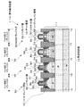
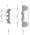
図95にCMOSセンサーのレイアウト図を示す。
図95に示すように、シリコン基板11に、フォトダイオードPDとこのフォトダイオードに接合するアクティブ領域15が形成されている。このアクティブ領域15に、転送ゲートTRG、リセットトランジスタRST、増幅トランジスタAmp、選択トランジスタSELが順に配置されている。また、転送ゲートTRGとリセットトランジスタRSTとの間にフローティングディフュージョン部FDが形成されている。
また、上記平面レイアウトの等価回路を図96に示す。図96に示すレイアウトでは、画素は、1つのフォトダイオードPDと、転送ゲートTRG、フローティングディフュージョン部FD、リセットトランジスタRST、増幅トランジスタAmp、選択トランジスタSELの4つのトランジスタから構成されている。これは、フォトダイオードPDを共有しないタイプであるが、もちろん共有するタイプや、4トランジスタ構成の部分が3トランジスタ構成のものもある。
FIG. 95 shows a layout diagram of the CMOS sensor.
As shown in FIG. 95, a photodiode PD and an
FIG. 96 shows an equivalent circuit of the planar layout. In the layout shown in FIG. 96, the pixel includes one photodiode PD and four transistors: a transfer gate TRG, a floating diffusion portion FD, a reset transistor RST, an amplification transistor Amp, and a selection transistor SEL. This is a type that does not share the photodiode PD, but of course there is a type that shares the photodiode PD and a part that has a 4-transistor configuration and a 3-transistor configuration.
解決しようとする問題点は、ランダムノイズ、白傷・暗電流を低減することが困難な点である。 The problem to be solved is that it is difficult to reduce random noise, white scratches and dark current.
本発明は、画素部のMOSトランジスタ上にて、異なる2層のシリサイドブロック膜の一部が重なるように形成して、ランダムノイズ、白傷・暗電流が低減することを可能にする。 The present invention makes it possible to reduce random noise, white scratches, and dark current by forming a part of two different layers of silicide block films on a MOS transistor in a pixel portion.
本発明の固体撮像装置は、半導体基板に、入射光を光電変換して電気信号を得る光電変換部を備えた画素部と前記画素部の周辺に形成された周辺回路部を有し、
前記画素部のMOSトランジスタのゲート電極の側壁にサイドウォール形成膜で形成された第1サイドウォールと、
前記周辺回路部のMOSトランジスタのゲート電極の側壁に前記サイドウォール形成膜と同一層の膜で形成された第2サイドウォールと、
前記光電変換部上および前記画素部のMOSトランジスタの一部上に前記サイドウォール形成膜と同一層の膜で形成された前記第1シリサイドブロック膜と、
前記画素部のMOSトランジスタ上に、前記第1シリサイドブロック膜の一部上に重なる第2シリサイドブロック膜を有し、
前記第1シリサイドブロック膜と前記第2シリサイドブロック膜とで前記画素部のMOSトランジスタ上が被覆されている。
The solid-state imaging device of the present invention has, on a semiconductor substrate, a pixel unit including a photoelectric conversion unit that photoelectrically converts incident light to obtain an electrical signal, and a peripheral circuit unit formed around the pixel unit,
A first sidewall formed of a sidewall formation film on a sidewall of the gate electrode of the MOS transistor of the pixel portion;
A second sidewall formed on the sidewall of the gate electrode of the MOS transistor of the peripheral circuit portion by a film of the same layer as the sidewall formation film;
The first silicide block film formed of the same layer film as the sidewall formation film on the photoelectric conversion unit and a part of the MOS transistor of the pixel unit;
A second silicide block film overlying a portion of the first silicide block film on the MOS transistor of the pixel portion;
The MOS transistor of the pixel portion is covered with the first silicide block film and the second silicide block film.
本発明の固体撮像装置では、サイドウォール形成膜と同一層の膜で形成された第1シリサイドブロック膜と、第1シリサイドブロック膜とは別の膜で形成された第2シリサイドブロック膜の2層で被覆されている。このため、画素部のMOSトランジスタ上が1層のシリサイドブロック膜で完全に被覆されるのではないので、ランダムノイズが低減され、白傷・暗電流が低減される。 In the solid-state imaging device of the present invention, the first silicide block film formed of the same layer as the sidewall formation film and the second silicide block film formed of a film different from the first silicide block film It is covered with. For this reason, the MOS transistor in the pixel portion is not completely covered with a single silicide block film, so that random noise is reduced, and white scratches and dark current are reduced.
本発明の固体撮像装置の製造方法は、半導体基板に、入射光を光電変換して電気信号を得る光電変換部を備えた画素部と前記画素部の周辺に形成された周辺回路部を形成する際に、
前記画素部と前記周辺回路部上を被覆するサイドウォール形成膜を形成する工程と、
前記画素部のMOSトランジスタのゲート電極の側壁に前記サイドウォール形成膜で第1サイドウォールを形成し、前記周辺回路部のMOSトランジスタのゲート電極の側壁に前記サイドウォール形成膜で第2サイドウォールを形成し、前記光電変換部上および前記画素部のMOSトランジスタの一部上に前記サイドウォール形成膜で第1シリサイドブロック膜を形成する工程と、
前記画素部のMOSトランジスタ上に、前記第1シリサイドブロック膜の一部上に重なる第2シリサイドブロック膜を形成する工程を有し、
前記第1シリサイドブロック膜と前記第2シリサイドブロック膜とで前記画素部のMOSトランジスタ上を被覆する。
According to the method for manufacturing a solid-state imaging device of the present invention, a pixel unit including a photoelectric conversion unit that photoelectrically converts incident light to obtain an electric signal and a peripheral circuit unit formed around the pixel unit are formed on a semiconductor substrate. When
Forming a sidewall forming film covering the pixel portion and the peripheral circuit portion;
A first sidewall is formed on the sidewall of the gate electrode of the MOS transistor in the pixel portion by the sidewall formation film, and a second sidewall is formed on the sidewall of the gate electrode of the MOS transistor in the peripheral circuit portion by the sidewall formation film. Forming a first silicide block film with the sidewall formation film on the photoelectric conversion portion and a part of the MOS transistor of the pixel portion;
Forming a second silicide block film overlying a part of the first silicide block film on the MOS transistor of the pixel portion;
The first silicide block film and the second silicide block film cover the MOS transistor of the pixel portion.
本発明の固体撮像装置の製造方法では、サイドウォール形成膜と同一層の膜で形成された第1シリサイドブロック膜と、第1シリサイドブロック膜とは別の膜で形成された第2シリサイドブロック膜の2層で被覆される。このため、画素部のMOSトランジスタ上が1層のシリサイドブロック膜で完全に被覆されるのではないので、ランダムノイズが低減され、白傷・暗電流が低減される。 In the method for manufacturing a solid-state imaging device of the present invention, the first silicide block film formed of the same layer as the sidewall formation film and the second silicide block film formed of a film different from the first silicide block film Are coated with two layers. For this reason, the MOS transistor in the pixel portion is not completely covered with a single silicide block film, so that random noise is reduced, and white scratches and dark current are reduced.
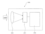
本発明の撮像装置では、入射光を集光する集光光学部と、
前記集光光学部で集光した光を受光して光電変換する固体撮像装置と、
光電変換された信号を処理する信号処理部を有し、
前記固体撮像装置は、
半導体基板に、入射光を光電変換して電気信号を得る光電変換部を備えた画素部と前記画素部の周辺に形成された周辺回路部を有し、
前記画素部のMOSトランジスタのゲート電極の側壁にサイドウォール形成膜で形成された第1サイドウォールと、
前記周辺回路部のMOSトランジスタのゲート電極の側壁に前記サイドウォール形成膜と同一層の膜で形成された第2サイドウォールと、
前記光電変換部上および前記画素部のMOSトランジスタの一部上に前記サイドウォール形成膜と同一層の膜で形成された第1シリサイドブロック膜と、
前記画素部のMOSトランジスタ上に、前記第1シリサイドブロック膜の一部上に重なる第2シリサイドブロック膜を有し、
前記第1シリサイドブロック膜と前記第2シリサイドブロック膜とで前記画素部のMOSトランジスタ上が被覆されている。
In the imaging device of the present invention, a condensing optical unit that condenses incident light;
A solid-state imaging device that receives and photoelectrically converts light collected by the condensing optical unit; and
A signal processing unit for processing the photoelectrically converted signal;
The solid-state imaging device
A semiconductor substrate has a pixel portion including a photoelectric conversion portion that photoelectrically converts incident light to obtain an electrical signal, and a peripheral circuit portion formed around the pixel portion,
A first sidewall formed of a sidewall formation film on a sidewall of the gate electrode of the MOS transistor of the pixel portion;
A second sidewall formed on the sidewall of the gate electrode of the MOS transistor of the peripheral circuit portion by a film of the same layer as the sidewall formation film;
A first silicide block film formed of a film of the same layer as the sidewall formation film on the photoelectric conversion unit and a part of the MOS transistor of the pixel unit;
A second silicide block film overlying a portion of the first silicide block film on the MOS transistor of the pixel portion;
The MOS transistor of the pixel portion is covered with the first silicide block film and the second silicide block film.
本発明の撮像装置では、本願発明の固体撮像装置を用いることから、ランダムノイズが低減され、白傷・暗電流が低減される。 In the imaging device of the present invention, since the solid-state imaging device of the present invention is used, random noise is reduced, and white scratches and dark current are reduced.
本発明の固体撮像装置は、ランダムノイズが低減でき、白傷・暗電流が低減できるという利点がある。 The solid-state imaging device of the present invention has advantages that random noise can be reduced and white scratches and dark current can be reduced.
本発明の固体撮像装置の製造方法は、ランダムノイズが低減でき、白傷・暗電流が低減できるという利点がある。 The manufacturing method of the solid-state imaging device of the present invention has the advantages that random noise can be reduced and white scratches and dark current can be reduced.
本発明の撮像装置は、本願発明の固体撮像装置を用いることから、各画素のランダムノイズが低減でき、白傷・暗電流が低減できる。よって、画質の向上が図れる。 Since the imaging device of the present invention uses the solid-state imaging device of the present invention, random noise of each pixel can be reduced, and white scratches and dark current can be reduced. Therefore, the image quality can be improved.
以下、発明を実施するための形態(以下、実施の形態とする)について説明する。 Hereinafter, modes for carrying out the invention (hereinafter referred to as embodiments) will be described.
<1.第1の実施の形態>
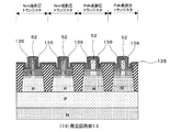
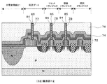
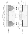
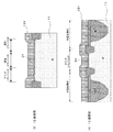
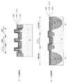
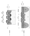
本発明の第1の実施の形態に係る固体撮像装置の構成の第1例を、図1の画素部の概略構成断面図、図2の周辺回路部の概略構成断面図および図5(1)の画素部の平面レイアウト図によって説明する。この図5(1)は、転送ゲートTRG、リセットトランジスタRST、増幅トランジスタAmp、選択トランジスタSELの活性領域でつながっている場合である。なお、図1に示した画素部および図2に示した周辺回路部は同一の半導体基板に形成されているものである。また、図1は図5(1)中のA−A線断面を示す。
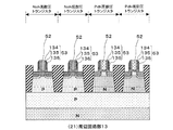
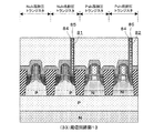
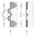
さらに、第1の実施の形態に係る固体撮像装置の構成の第2例を、図3の画素部の概略構成断面図、図4の周辺回路部の概略構成断面図および図5(2)の画素部の平面レイアウト図によって説明する。この図5(2)は、転送ゲートTRG、リセットトランジスタRST、増幅トランジスタAmp、選択トランジスタSELの活性領域がSTIによって分離されている場合である。なお、図3に示した画素部および図4に示した周辺回路部は同一の半導体基板に形成されているものである。また、図3は図5(2)中のB−B線断面を示す。
同飽和電荷量Qsで画素サイズを小さくするためには、図5(1)のレイアウトが望ましい。
<1. First Embodiment>
FIG. 5 is a schematic configuration cross-sectional view of a pixel unit in FIG. 1, a schematic configuration cross-sectional view of a peripheral circuit unit in FIG. 2, and FIG. 5 (1), illustrating a first example of a configuration of a solid-state imaging device according to a first embodiment of the present invention. This will be described with reference to a plan layout diagram of the pixel portion. FIG. 5A shows a case where the active regions of the transfer gate TRG, the reset transistor RST, the amplification transistor Amp, and the selection transistor SEL are connected. The pixel portion shown in FIG. 1 and the peripheral circuit portion shown in FIG. 2 are formed on the same semiconductor substrate. Moreover, FIG. 1 shows the AA line cross section in FIG. 5 (1).
Further, a second example of the configuration of the solid-state imaging device according to the first embodiment is illustrated in a schematic configuration cross-sectional view of the pixel portion in FIG. 3, a schematic configuration cross-sectional view of the peripheral circuit portion in FIG. 4, and FIG. This will be described with reference to a plan layout diagram of the pixel portion. FIG. 5B shows the case where the active regions of the transfer gate TRG, the reset transistor RST, the amplification transistor Amp, and the selection transistor SEL are separated by STI. The pixel portion shown in FIG. 3 and the peripheral circuit portion shown in FIG. 4 are formed on the same semiconductor substrate. Moreover, FIG. 3 shows the BB line cross section in FIG. 5 (2).
In order to reduce the pixel size with the same saturation charge amount Qs, the layout of FIG. 5A is desirable.
[固体撮像装置の構成の第1例]
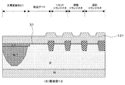
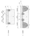
図1、図2および図5(1)に示すように、半導体基板11に、入射光を光電変換して電気信号を得る光電変換部21を備えた画素部12と、この画素部12の周辺に形成された周辺回路部13を有する。
上記画素部12の半導体基板11には、光電変換部21が形成され、この光電変換部21に接続して転送ゲートTRG、リセットトランジスタRST、増幅トランジスタAmp、選択トランジスタSELが順に直列に形成されている。上記光電変換部21は例えばフォトダイオードで構成されている。
[First Example of Configuration of Solid-State Imaging Device]
As shown in FIGS. 1, 2, and 5 (1), a pixel unit 12 including a
A
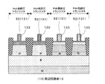
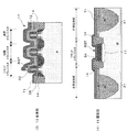
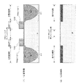
上記画素部12のMOSトランジスタ30(転送ゲートTRG、リセットトランジスタRST、増幅トランジスタAmp、選択トランジスタSEL)の各ゲート電極32の側壁には、サイドウォール形成膜で第1サイドウォール33が形成されている。
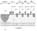
また上記周辺回路部13の各MOSトランジスタ50のゲート電極52の側壁に配線上記サイドウォール形成膜と同一層の膜で第2サイドウォール53が形成されている。
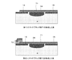
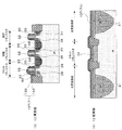
さらに上記光電変換部21上には、上記サイドウォール形成膜と同一層の膜で第1シリサイドブロック膜71が形成されている。
また、上記画素部12の各MOSトランジスタ30上には、上記第1シリサイドブロック膜71の一部上に重なる第2シリサイドブロック膜72を有する。
上記第1シリサイドブロック膜71は、例えば酸化シリコン膜と窒化シリコン膜との積層構造を有している。
また、第2シリサイドブロック膜72は、例えば酸化シリコン膜と窒化シリコン膜との積層構造を有している。
そして、上記第1シリサイドブロック膜71を上記第2シリサイドブロック膜72とで上記画素部12上が被覆されている。この上記第1シリサイドブロック膜71と上記第2シリサイドブロック膜72の重なり部分は上記画素部12内に形成されている。
On the side walls of the
A
Further, a first
Further, a second
The first
The second
The pixel portion 12 is covered with the first
上記周辺回路部13の各MOSトランジスタ50は、例えばゲート電極52上、ソース・ドレイン領域54、55上にシリサイド層56、57が形成されている。このように、上記周辺回路13の各MOSトランジスタ50は、寄生抵抗を減らし高速動作させるため、シリサイド化されている。
In each
また、上記半導体基板11には、上記画素部12を分離する第1素子分離領域14が形成され、上記周辺回路部13内の各MOSトランジスタの形成領域を分離する第2素子分離領域15が形成されている。
上記第1素子分離領域14および上記第2素子分離領域15はともにSTI構造を有し、上記第1素子分離領域14は、上記第2素子分離領域15よりも浅く、かつ上記半導体基板11上への突き出し高さが低く形成されている。
In addition, a first
Both the first
このように、上記固体撮像装置1(1A)では、サイドウォール形成膜を使って第1シリサイドブロック膜71が形成された領域と、別途にシリサイドブロック用の絶縁膜を設けて形成した第2シリサイドブロック膜72が形成された領域と、周辺回路部13のMOSトランジスタ50のように、シリサイド層56、57が存在する領域が混在する。また光電変換部21上は、サイドウォール形成膜を利用して第1シリサイドブロック膜71が形成されている。
As described above, in the solid-state imaging device 1 (1A), the region where the first
[固体撮像装置の構成の第2例]
また、図3、図4および図5(2)に示すように、半導体基板11に、入射光を光電変換して電気信号を得る光電変換部21を備えた画素部12と、この画素部12の周辺に形成された周辺回路部13を有する。
上記画素部12の半導体基板11には、光電変換部21が形成され、この光電変換部21に接続して転送ゲートTRG、リセットトランジスタRST、増幅トランジスタAmp、選択トランジスタSELが順に直列に形成されている。上記光電変換部21は例えばフォトダイオードで構成されている。
[Second Example of Configuration of Solid-State Imaging Device]
3, 4, and 5 (2), the pixel unit 12 includes a
A
上記画素部12のMOSトランジスタ30(転送ゲートTRG、リセットトランジスタRST、増幅トランジスタAmp、選択トランジスタSEL)の各ゲート電極32の側壁には、サイドウォール形成膜で第1サイドウォール33が形成されている。
また上記周辺回路部13の各MOSトランジスタ50のゲート電極52の側壁に配線上記サイドウォール形成膜と同一層の膜で第2サイドウォール53が形成されている。
さらに上記光電変換部21上には、上記サイドウォール形成膜と同一層の膜で第1シリサイドブロック膜71が形成されている。
また、上記画素部12の各MOSトランジスタ30上には、上記第1シリサイドブロック膜71の一部上に重なる第2シリサイドブロック膜72を有する。
上記第1シリサイドブロック膜71は、例えば酸化シリコン膜と窒化シリコン膜との積層構造を有している。
また、第2シリサイドブロック膜72は、例えば酸化シリコン膜と窒化シリコン膜との積層構造を有している。
そして、上記第1シリサイドブロック膜71を上記第2シリサイドブロック膜72とで上記画素部12上が被覆されている。この上記第1シリサイドブロック膜71と上記第2シリサイドブロック膜72の重なり部分は上記画素部12内に形成されている。
On the side walls of the
A
Further, a first
Further, a second
The first
The second
The pixel portion 12 is covered with the first
上記周辺回路部13の各MOSトランジスタ50は、例えばゲート電極52上、ソース・ドレイン領域54、55上にシリサイド層56、57が形成されている。このように、上記周辺回路13の各MOSトランジスタ50は、寄生抵抗を減らし高速動作させるため、シリサイド化されている。
In each
また、上記半導体基板11には、上記画素部12内の各MOSトランジスタの形成領域を分離する第1素子分離領域14が形成され、上記周辺回路部13内の各MOSトランジスタの形成領域を分離する第2素子分離領域15が形成されている。
上記第1素子分離領域14および上記第2素子分離領域15はともにSTI構造を有し、上記第1素子分離領域14は、上記第2素子分離領域15よりも浅く、かつ上記半導体基板11上への突き出し高さが低く形成されている。
The
Both the first
このように、上記固体撮像装置1(1B)では、サイドウォール形成膜を使って第1シリサイドブロック膜71が形成された領域と、別途にシリサイドブロック用の絶縁膜を設けて形成した第2シリサイドブロック膜72が形成された領域と、周辺回路部13のMOSトランジスタ50のように、シリサイド層56、57が存在する領域が混在する。また光電変換部21上は、サイドウォール形成膜を利用して第1シリサイドブロック膜71が形成されている。
As described above, in the solid-state imaging device 1 (1B), the region where the first
上記固体撮像装置1(1A、1B)では、画素部12内は、シリサイド起因の不純物汚染、欠陥の発生を抑制するために、望ましくは、完全に第1シリサイドブロック膜71と第2シリサイドブロック膜72とで被覆されていることが望ましい。また、素子分離領域14、15上は、上記第1、第2シリサイドブロック膜71、72が形成されていなくてもよい。しかしながら、同画素サイズで光電変換部21の受光面積をできるだけ大きくして、飽和電荷量(Qs)を多くし、ノイズの影響を小さくする必要がある。したがって、素子分離領域上での合わせ余裕を考慮する必要がないように、素子分離領域上も第1シリサイドブロック膜71と第2シリサイドブロック膜72とで被覆されていることが望ましい。このようにすることで、素子分離領域の面積が削減でき、光電変換部21の受光面積を大きくとることが可能になる。
In the solid-state imaging device 1 (1A, 1B), it is desirable that the first
そこで、上記固体撮像装置1のレイアウトでは、素子分離領域の分離幅を狭くしてフォトダイオードの占める割合を大きくするために、第1、第2シリサイドブロック膜71、72が重なった部分を設けている。そのため、画素部12の各ゲート電極32上の段差が大きくなり、層間絶縁膜の平坦性が厳しくなる。
例えば、特開2005-347325号公報に記載されている分離技術では、画素内の酸化膜分離のシリコン(Si)表面からの突き出し量が高くなり、平坦性の難易度が高くなる。
本発明では、STI(Shallow Trench Isolation)構造の第1素子分離領域14を用い、半導体基板11上に突き出す高さを低くしている。ただし、第1素子分離領域14は、STI深さが周辺回路部13の第2素子分離領域15のSTIと同等の深さであると、光電変換部21を構成するフォトダイオードに対するストレスやエッチングダメージが多くなり、白傷の増加を招く。そのため、第1素子分離領域14は、周辺回路部13の第2素子分離領域15よりも浅く形成している。高速動作を実現するために周辺回路部13の第2素子分離領域15はSTI深さを深くして、配線・基板間の寄生容量を低減させている。
Therefore, in the layout of the solid-
For example, in the separation technique described in Japanese Patent Application Laid-Open No. 2005-347325, the amount of protrusion from the silicon (Si) surface of the oxide film separation in the pixel increases, and the difficulty of flatness increases.
In the present invention, a first
本発明の固体撮像装置1(1A)では、サイドウォール形成膜と同一層の膜で形成された第1シリサイドブロック膜71と、第1シリサイドブロック膜71とは別の膜で形成された第2シリサイドブロック膜72の2層で画素部12が被覆されている。このため、画素部12のMOSトランジスタ30上が1層のシリサイドブロック膜で完全に被覆されるのではないので、ランダムノイズが低減され、白傷・暗電流が低減できるという利点がある。
In the solid-state imaging device 1 (1A) of the present invention, the first
<2.第2の実施の形態>
[固体撮像装置の製造方法の第1例]
次に、本発明の固体撮像装置の製造方法に係る一実施の形態の第1例を、図6〜図39の製造工程断面図によって説明する。
<2. Second Embodiment>
[First Example of Manufacturing Method of Solid-State Imaging Device]
Next, a first example of an embodiment according to a method for manufacturing a solid-state imaging device of the present invention will be described with reference to manufacturing process cross-sectional views of FIGS.
図6(1)に示すように、半導体基板11には例えばシリコン基板を用いる。
上記半導体基板11上にパッド酸化膜111、窒化シリコン膜112を形成する。
上記パッド酸化膜111は、例えば熱酸化法により、半導体基板11表面を酸化して形成する。このパッド酸化膜111は、例えば15nmの厚さに形成する。
次に、例えばLP−CVD(Low Pressure CVD)法により、上記パッド酸化膜111条に窒化シリコン膜112を形成する。この窒化シリコン膜112は、例えば160nmの厚さに形成される。
上記説明した構成では、窒化シリコン膜/パッド酸化膜の構造であるが、窒化シリコン膜/ポリシリコン膜またはアモルファスシリコン膜/パッド酸化膜の構造であっても良い。
As shown in FIG. 6A, for example, a silicon substrate is used as the
A
The
Next, a
In the configuration described above, the structure is a silicon nitride film / pad oxide film, but may be a structure of silicon nitride film / polysilicon film or amorphous silicon film / pad oxide film.
次に、図7(2)に示すように、上記窒化シリコン膜112上に素子分離領域を形成する領域上に開口部を設けたレジストマスク(図示せず)を形成した後、エッチングによって上記窒化シリコン膜112および上記パッド酸化膜111に開口部113を形成する。
上記エッチングでは、例えば反応性イオンエッチング(RIE:Reactive Ion Etching)装置または電子サイクロトロン共鳴(ECR:Electron Cyclotron Resonance)エッチング装置などを用いることができる。加工後、アッシング装置などにより上記レジストマスクの除去を行う。
Next, as shown in FIG. 7B, a resist mask (not shown) having an opening is formed on the
In the etching, for example, a reactive ion etching (RIE) apparatus or an electron cyclotron resonance (ECR) etching apparatus can be used. After the processing, the resist mask is removed by an ashing device or the like.
次に、図8(3)に示すように、上記窒化シリコン膜112をエッチングマスクに用いて、上記半導体基板11に素子分離溝114を形成する。このエッチングには、例えばRIE装置またはECRエッチング装置などを用いる。
まず、周辺回路部13(および画素部12)の第2素子分離溝115(および第1素子分離溝114)の第1エッチングを行う。このとき、周辺回路部13(および画素部12)の各第1、第2素子分離溝114、115の深さは50nm〜160nmである。
図示はしないが画素部12上にレジストマスクを形成し、さらに周辺回路部13のみ素子分離溝115を延長形成する第2エッチングを行い、周辺回路部13のみ第2素子分離溝115の深さを、例えば0.3μmに形成する。その後、レジストマスクを除去する。
Next, as shown in FIG. 8C,
First, the first etching of the second element isolation trench 115 (and the first element isolation trench 114) of the peripheral circuit portion 13 (and the pixel portion 12) is performed. At this time, the depths of the first and second
Although not shown in the drawing, a resist mask is formed on the pixel portion 12, and second etching is performed to extend the
このように、画素部12の素子分離溝114を浅くすることにより、エッチングダメージによる白傷を抑制する効果がある。素子分離溝114を浅くすることで、実効的な光電変換部の面積が増えるため、飽和電荷量(Qs)が大きくなる効果がある。
Thus, by making the
次に、図示はしないが、ライナー膜を形成する。このライナー膜は、例えば約800℃〜900℃の熱酸化で形成される。上記ライナー膜は、酸化シリコン膜、窒素を含んだ酸化シリコン膜またはCVD窒化シリコン膜でもよい。その膜厚は、約4nm〜10nmとする。
また図示はしないが、レジストマスクを用いて画素部12に暗電流抑制するためのホウ素(B)をイオン注入する。そのイオン注入条件は、一例として、打ち込みエネルギーを10keV程度に設定し、ドーズ量を1×10¹²/cm2〜1×1014/cm2に設定して行う。画素部12内の素子分離領域が形成される第1素子分離溝114の周りは、ホウ素濃度が高いほど、暗電流が抑制され、寄生トランジスタ動作が抑制される。しかし、ホウ素の濃度を高くしすぎると、光電変換部を形成するフォトダイオードの面積が小さくなり、飽和電荷量(Qs)が小さくなるので、上記ドーズ量としている。
Next, although not shown, a liner film is formed. This liner film is formed by thermal oxidation at about 800 ° C. to 900 ° C., for example. The liner film may be a silicon oxide film, a silicon oxide film containing nitrogen, or a CVD silicon nitride film. The film thickness is about 4 nm to 10 nm.
Although not shown, boron (B) for suppressing dark current is ion-implanted into the pixel portion 12 using a resist mask. As an example of the ion implantation conditions, the implantation energy is set to about 10 keV, and the dose is set to 1 × 10 12 / cm 2 to 1 × 10 14 / cm 2 . Around the first
次に、図9(4)に示すように、上記第2素子分離溝115(および第1素子分離溝114)の内部を埋め込むように、上記窒化シリコン膜112上に絶縁膜を形成する。この絶縁膜は、例えば高密度プラズマCVD法によって酸化シリコンを堆積して形成する。
次いで、上記窒化シリコン膜112上の余剰な上記絶縁膜を、例えば化学的機械研磨(CMP:Chemical Mechanical Polishing)によって除去し、第2素子分離溝115(第1素子分離溝114)の内部に残して上記絶縁膜で第2素子分離領域15(第1素子分離領域14)を形成する。上記CMPでは、窒化シリコン膜112がストッパとなって、CMPを停止させる。
第1素子分離領域14は、周辺回路部13の第2素子分離領域15よりも浅く形成しているが、窒化シリコン膜112のストッパが同じであるため、素子分離の突き出し量は、同じに設定される。ここで、第1素子分離領域14と第2素子分離領域15の突出高さが同じ突出高さとは、製造加工精度に基づく加工ばらつきの範囲内であれば、同じ突出高さであると定義する。すなわち、溝(トレンチ)加工でのマスクとして用いる窒化シリコン膜112の膜厚は、一般的に160nm程度の窒化シリコン膜でウエハの面内ばらつきが±10%程度ある。CMP(化学機械研磨)による研磨ばらつきについても、±20〜30nm程度ある。したがって、画素部12と周辺回路部13が同じになるように工夫しても、20nm〜30nm程度変動する可能性がある。厳密に観察してチップ面内のどこかで画素部12と周辺回路部13を比較した場合、完全に同じ突出高さでないとしても、画素部と周辺回路部において両突出高さとの差が30nm以内に入っていれば、本発明でいう「同じ高さ」の範疇に入ることは言うまでもない。
最終的には、第1素子分離領域14と第2素子分離領域15の突き出し量の高さは、一例としてシリコン表面から0〜20nm程度にセンター条件が低く設定される。
Next, as shown in FIG. 9 (4), an insulating film is formed on the
Next, the excessive insulating film on the
The first
Finally, the height of the protruding amount of the first
次に、図10(5)に示すように、半導体基板11表面からの第1素子分離領域14の高さを調整するために、酸化膜のウエットエッチを行う。酸化膜のエッチング量は例えば40nm〜100nmとする。
本発明では、STI(Shallow Trench Isolation)構造の第1素子分離領域14を用い、半導体基板11上に突き出す高さを低くしている。ただし、第1素子分離領域14は、STI深さが周辺回路部13の第2素子分離領域15のSTIと同等の同じ深さであると、光電変換部21を構成するフォトダイオードに対するストレスやエッチダメージが多くなり、白傷の増加を招く。そのため、第1素子分離領域14は、周辺回路部13の第2素子分離領域15よりも浅く形成している。高速動作を実現するために周辺回路部13の第2素子分離領域15はSTI深さを深くして、配線・基板間の寄生容量を低減させている。
次いで上記窒化シリコン膜112(前記図7(4)参照)を除去し、パッド酸化膜111を露出させる。上記窒化シリコン膜112は、例えば熱リン酸によるウエットエッチングにより除去される。
Next, as shown in FIG. 10 (5), in order to adjust the height of the first
In the present invention, a first
Next, the silicon nitride film 112 (see FIG. 7 (4)) is removed, and the
次に、図11(6)に示すように、pウエルを形成する領域上に開口部を設けたレジストマスク(図示せず)を用いて、パッド酸化膜111を形成した状態で、イオン注入により、半導体基板11にpウエル121を形成する。さらに、チャネルイオン注入を行う。その後、上記レジストマスクを除去する。
また、nウエルを形成する領域上に開口部を設けたレジストマスク(図示せず)を用いて、パッド酸化膜111を形成した状態で、イオン注入により、半導体基板11にnウエル123を形成する。さらに、チャネルイオン注入を行う。その後、上記レジストマスクを除去する。
上記pウエル121は、イオン注入種にホウ素(B)を用い、打ち込みエネルギーを例えば200keV、ドーズ量を例えば1×1013cm-2に設定して行う。上記pウエル121のチャネルイオン注入は、イオン注入種にホウ素(B)を用い、打ち込みエネルギーを例えば10keV〜20keV、ドーズ量を例えば1×1011cm-2〜1×1013cm-2に設定して行う。
上記nウエル123は、イオン注入種に例えばリン(P)を用い、打ち込みエネルギーを例えば200keV、ドーズ量を例えば1×1013cm-2に設定して行う。上記nウエル123のチャネルイオン注入は、イオン注入種に例えばヒ素(As)を用い、打ち込みエネルギーを例えば100keV、ドーズ量を例えば1×1011cm-2〜1×1013cm-2に設定して行う。
また、図示はしないが、次に、光電変換部にフォトダイオードを形成するイオン注入を行い、p型領域を形成する。例えば、光電変換部が形成される半導体基板の表面には、ホウ素(B)のイオン注入を行い、深い領域にヒ素(As)もしくはリン(P)を用いてイオン注入を行い、上記p型領域の下部に接合するn型領域を形成する。このようにして、pn接合の光電変換部を形成する。
Next, as shown in FIG. 11 (6), ion implantation is performed in a state where a
Further, an
The p-well 121 is formed by using boron (B) as an ion implantation species, setting the implantation energy to, for example, 200 keV, and setting the dose to, for example, 1 × 10 13 cm −2 . In the channel ion implantation of the p-well 121, boron (B) is used as an ion implantation species, the implantation energy is set to, for example, 10 keV to 20 keV, and the dose is set to, for example, 1 × 10 11 cm −2 to 1 × 10 13 cm −2 . And do it.
The n-well 123 is formed by using, for example, phosphorus (P) as an ion implantation species, setting the implantation energy to 200 keV, and setting the dose to 1 × 10 13 cm −2 , for example. The channel ion implantation of the n-well 123 uses, for example, arsenic (As) as an ion implantation species, an implantation energy of, for example, 100 keV, and a dose of, for example, 1 × 10 11 cm −2 to 1 × 10 13 cm −2. Do it.
Although not shown, ion implantation for forming a photodiode in the photoelectric conversion portion is performed next to form a p-type region. For example, boron (B) ions are implanted into the surface of the semiconductor substrate on which the photoelectric conversion portion is formed, arsenic (As) or phosphorus (P) is implanted into a deep region, and the p-type region is formed. An n-type region is formed to be bonded to the lower part of the substrate. In this way, a pn junction photoelectric conversion part is formed.
次に、図12(7)に示すように、パッド酸化膜111(前記図11(6)参照)を、例えばウエットエッチングにより除去する。
次に、半導体基板11上に、高電圧用の厚膜のゲート絶縁膜51Hを形成する。膜厚は、電源電圧3.3V用トランジスタで約7.5nm、2.5V用トランジスタで約5.5nmとする。次いで、高電圧用の厚膜のゲート絶縁膜51H上にレジストマスク(図示せず)を形成し、低電圧用トランジスタ領域に形成された厚膜のゲート絶縁膜51Hを除去する。
上記レジストマスクを除去した後、半導体基板11上に、低電圧用トランジスタ領域に薄膜のゲート絶縁膜51Lを形成する。膜厚は、電源電圧1.0V用トランジスタで約1.2nm〜1.8nmとする。同時に画素部のトランジスタ形成領域にも、薄膜のゲート絶縁膜31(図示せず)が形成される。
上記ゲート絶縁膜51H、51L、31は、例えば熱酸化シリコン膜で形成されている。もしくは、RTO(Rapid Thermal Oxidation)を用いた酸窒化シリコン膜でも良い。また、ゲートリークをさらに低減するために、ハフニウム(Hf)やジルコニウム(Zr)などの酸化膜、酸窒化膜等の高誘電体膜を用いてもよい。
以後、図示では、便宜上、厚膜のゲート絶縁膜51Hと薄膜のゲート絶縁膜51Lとを同等の膜厚に描いている。
Next, as shown in FIG. 12 (7), the pad oxide film 111 (see FIG. 11 (6)) is removed by, for example, wet etching.
Next, a thick
After removing the resist mask, a thin
The
Thereafter, in the drawing, for the sake of convenience, the thick
次に、図13(8)の画素部の断面図および図14(9)の周辺回路部の断面図に示すように、ゲート絶縁膜51(51H、51L)、ゲート絶縁膜31上にゲート電極形成膜131を形成する。上記ゲート電極形成膜131は、例えばLP−CVD法により、ポリシリコンを堆積して形成する。堆積膜厚は、技術ノードにもよるが、90nmノードでは、150nm〜200nmとする。
また、膜厚は、加工の制御性から一般にゲートアスペクト比を大きくしないため、ノード毎に薄くなる傾向にある。
そして、ゲート空乏化対策として、ポリシリコンの代わりにシリコンゲルマニウム(SiGe)を用いてよい。このゲート空乏化とは、ゲート酸化膜の膜厚が薄膜化するに伴い、物理的なゲート酸化膜の膜厚だけでなくゲートポリシリコン内の空乏層の膜厚の影響が無視できなくなって、実効的なゲート酸化膜の膜厚が薄くならず、トランジスタ性能が落ちてしまうという問題である。
Next, as shown in the cross-sectional view of the pixel portion in FIG. 13 (8) and the cross-sectional view of the peripheral circuit portion in FIG. 14 (9), a gate electrode is formed on the gate insulating film 51 (51H, 51L) and the
In addition, the film thickness tends to become thinner at each node because the gate aspect ratio is generally not increased from the controllability of processing.
As a gate depletion countermeasure, silicon germanium (SiGe) may be used instead of polysilicon. This gate depletion means that as the thickness of the gate oxide film becomes thinner, not only the physical gate oxide film thickness but also the influence of the thickness of the depletion layer in the gate polysilicon cannot be ignored. This is a problem that the effective gate oxide film thickness is not reduced and the transistor performance is degraded.
次に、図15(10)の画素部の断面図および図16(11)の周辺回路部の断面図に示すように、ゲート空乏化対策を行う。まず、pMOSトランジスタの形成領域上にレジストマスク132を形成し、nMOSトランジスタの形成領域の上記ゲート電極形成膜131にn型不純物をドーピングする。このドーピングは、例えばリン(P)またはヒ素(As)をイオン注入して行う。イオン注入量は、約1×10¹⁵/cm2〜1×1016/cm2である。その後、上記レジストマスク132を除去する。
次いで、図示はしていないが、nMOSトランジスタの形成領域上にレジストマスク(図示せず)を形成し、pMOSトランジスタの形成領域の上記ゲート電極形成膜131にp型不純物をドーピングする。このドーピングは、例えばホウ素(B)または二フッ化ホウ素(BF2)またはインジウム(In)をイオン注入して行う。イオン注入量は、約1×10¹⁵/cm2〜1×1016/cm2である。その後、上記レジストマスクを除去する。
上記イオン注入は、どちらを先に行ってもよい。
また、上記各イオン注入において、イオン注入した不純物がゲート絶縁膜の直下に突き抜けるのを防ぐために、窒素(N2)のイオン注入を組み合わせても良い。
Next, as shown in the cross-sectional view of the pixel portion in FIG. 15 (10) and the cross-sectional view of the peripheral circuit portion in FIG. 16 (11), gate depletion measures are taken. First, a resist
Next, although not shown, a resist mask (not shown) is formed on the nMOS transistor formation region, and the gate
Either of the ion implantations may be performed first.
Further, in each of the above ion implantations, nitrogen (N 2 ) ion implantation may be combined in order to prevent the implanted ions from penetrating directly under the gate insulating film.
次に、図17(12)の画素部の断面図および図18(13)の周辺回路部の断面図に示すように、上記ゲート電極形成膜131上に各ゲート電極を形成するためのレジストマスク(図示せず)を形成する。このレジストマスクをエッチングマスクに用いた反応性イオンエッチングによって、上記ゲート電極形成膜131上をエッチング加工して画素部12の各MOSトランジスタのゲート電極32、周辺回路部13の各MOSトランジスタのゲート電極52を形成する。
次いで、上記各ゲート電極32、52の表面を酸化して酸化膜133を形成する。
上記酸化膜133の膜厚は、例えば1nm〜10nmとする。また、上記酸化膜133は、上記ゲート電極32、52の側壁とともに上面にも形成されている。
さらに、上記酸化工程によって、上記ゲート電極32、52のエッジ部分を丸めることによって、酸化膜耐圧を改善することができる効果がある。
また、上記熱処理が行われることによって、エッチダメージを低減することができる。
また、上記ゲート電極加工において、光電変換部21上に形成されていた上記ゲート絶縁膜が除去されたとしても、光電変換部21上にも上記酸化膜133が形成される。このため、次工程のリソグラフィー技術においてレジスト膜を形成した際に、シリコン表面に直付けではなくなるために、このレジストによる汚染を防止できる。よって、画素部12の光電変換部21にとっては、白傷防止対策になる。
Next, as shown in the cross-sectional view of the pixel portion in FIG. 17 (12) and the cross-sectional view of the peripheral circuit portion in FIG. 18 (13), a resist mask for forming each gate electrode on the gate
Next, the surface of each of the
The film thickness of the
Furthermore, the oxide film withstand voltage can be improved by rounding the edge portions of the
Further, etch damage can be reduced by performing the heat treatment.
In the gate electrode processing, even if the gate insulating film formed on the
次に、図19(14)の画素部の断面図および図20(15)の周辺回路部の断面図に示すように、画素部12の各MOSトランジスタのLDD領域38、39等を形成するとともに、周辺回路部13の各MOSトランジスタのLDD領域61、62、63、64等を形成する。
Next, as shown in the cross-sectional view of the pixel portion in FIG. 19 (14) and the cross-sectional view of the peripheral circuit portion in FIG. 20 (15), the
まず、周辺回路部13に形成されるNMOSトランジスタに関しては、各ゲート電極52(52N)の両側における半導体基板11にポケット拡散層65、66を形成する。このポケット拡散層65、66は、イオン注入により形成され、イオン注入種に例えば二フッ化ホウ素(BF2)またはホウ素(B)またはインジウム(In)を用い、ドーズ量を例えば1×10¹²/cm2〜1×1014/cm2に設定する。
さらに各ゲート電極52(52N)の両側における半導体基板11にLDD領域61、62を形成する。LDD領域61、62は、イオン注入により形成され、イオン注入種に例えばヒ素(As)もしくはリン(P)を用い、ドーズ量を例えば1×10¹³/cm2〜1×1015/cm2に設定する。
First, for the NMOS transistor formed in the peripheral circuit section 13, pocket diffusion layers 65 and 66 are formed in the
Further,
上記画素部12に形成されるMOSトランジスタに関しては、各ゲート電極32の両側における半導体基板11にLDD領域38、39を形成する。LDD領域38、39は、イオン注入により形成され、イオン注入種に例えばヒ素(As)もしくはリン(P)を用い、ドーズ量を例えば1×10¹³/cm2〜1×1015/cm2に設定する。また、ポケット拡散層を形成してもよい。
上記画素部12に形成されるMOSトランジスタに関しては、工程削減の観点から、LDD領域を形成しなくてもよい。もしくは、周辺回路部13に形成されるMOSトランジスタのLDDイオン注入と兼ねてもよい。
With respect to the MOS transistor formed in the pixel portion 12,
With respect to the MOS transistor formed in the pixel portion 12, the LDD region may not be formed from the viewpoint of process reduction. Alternatively, it may also serve as LDD ion implantation of a MOS transistor formed in the peripheral circuit section 13.
周辺回路部13のPMOSトランジスタの形成領域に関しては、各ゲート電極52の両側における半導体基板11にポケット拡散層67、68を形成する。このポケット拡散層67、68は、イオン注入により形成され、イオン注入種に例えばヒ素(As)またはリン(P)を用い、ドーズ量を例えば1×10¹²/cm2〜1×1014/cm2に設定する。
さらに各ゲート電極52(52P)の両側における半導体基板11にLDD領域63、64を形成する。LDD領域63、64は、イオン注入により形成され、イオン注入種に例えば二フッ化ホウ素(BF2)またはホウ素(B)またはインジウム(In)を用い、ドーズ量を例えば1×10¹³/cm2〜1×1015/cm2に設定する。
Regarding the formation region of the PMOS transistor in the peripheral circuit portion 13, pocket diffusion layers 67 and 68 are formed in the
Further,
また、周辺回路部のNMOSトランジスタ、PMOSトランジスタのポケットイオン注入前に、注入のチャネリング抑制技術として、ゲルマニウム(Ge)をイオン注入することなどでプリアモルファス化を行ってもよい。また、LDD領域形成後、TED(Transient Enhanced Diffusion)などを引き起こす注入欠陥を小さくするために、800℃〜900℃程度のRTA(Rapid Thermal Annealing)処理を追加してもよい。 Further, pre-amorphization may be performed by implanting germanium (Ge) as a channeling suppression technique for implantation before pocket ion implantation of the NMOS transistor and PMOS transistor in the peripheral circuit portion. Further, after the formation of the LDD region, an RTA (Rapid Thermal Annealing) process of about 800 ° C. to 900 ° C. may be added in order to reduce implantation defects that cause TED (Transient Enhanced Diffusion) or the like.
次に、図21(16)の画素部の断面図および図22(17)の周辺回路部の断面図に示すように、画素部12および周辺回路部13の全面に酸化シリコン(SiO2)膜134を形成する。この酸化シリコン膜134は、ノンドープトシリケートガラス(NSG)またはLP−TEOS(Tetra Ethyl Ortho Silicate)または高温酸化(HTO)膜等の堆積膜で形成される。上記酸化シリコン膜134は、例えば5nm〜20nmの膜厚に形成される。
次に、上記酸化シリコン膜134上に窒化シリコン膜135を形成する。この窒化シリコン膜135は、例えばLPCVDにて形成された窒化シリコン膜を用いる。その膜厚は、例えば10nm〜100nmとする。
上記窒化シリコン膜135は、低温で成膜できる原子層蒸着法により成膜されたALD窒化シリコン膜でもよい。
上記窒化シリコン膜135の直下の上記酸化シリコン膜134は、画素部12の光電変換部21上では、その膜厚が薄いほど、光反射を防ぐので、光電変換部21の感度が良くなる。
次に、必要に応じて、上記窒化シリコン膜135上に3層目の酸化シリコン(SiO2)膜136を堆積する。この酸化シリコン膜136は、NSGまたはLP−TEOSまたはHTO等の堆積膜で形成される。この酸化シリコン膜136は、例えば10nm〜100nmの膜厚に形成される。
Next, as shown in the cross-sectional view of the pixel portion in FIG. 21 (16) and the cross-sectional view of the peripheral circuit portion in FIG. 22 (17), a silicon oxide (SiO 2 ) film is formed on the entire surface of the pixel portion 12 and the peripheral circuit portion 13. 134 is formed. The
Next, a
The
Since the
Next, a third silicon oxide (SiO 2 )
したがって、サイドウォール形成膜137は、酸化シリコン膜136/窒化シリコン膜135/酸化シリコン膜134の3層構造膜となる。なお、このサイドウォール形成膜137は、窒化シリコン膜/酸化シリコン膜の2層構造膜であってもよい。以下、3層構造膜のサイドウォール形成膜137で説明する。
Therefore, the
次に、図23(18)の画素部の断面図および図24(19)の周辺回路部の断面図に示すように、最上層に形成されている上記酸化シリコン膜136をエッチバックして、各ゲート電極32、52等の側部側にのみ残す。上記エッチバックは、例えば反応性イオンエッチング(RIE)によって行う。このエッチバックでは、上記窒化シリコン膜135でエッチングを停止する。このように、窒化シリコン膜135でエッチングを停止するため、画素部12の光電変換部21へのエッチダメージを低減することができるので、白傷を低減することができる。
Next, as shown in the cross-sectional view of the pixel portion in FIG. 23 (18) and the cross-sectional view of the peripheral circuit portion in FIG. 24 (19), the
次に、図25(20)の画素部の断面図および図26(21)の周辺回路部の断面図に示すように、画素部12の光電変換部21上の全面および転送ゲートTRG上の一部にかかるように、レジストマスク138を形成する。
その後、上記窒化シリコン膜135、上記酸化シリコン膜134をエッチバックして、各ゲート電極32、52の側壁部に酸化シリコン膜134、窒化シリコン膜135、酸化シリコン膜136からなる第1サイドウォール33、第2サイドウォール53を形成する。このとき、光電変換部21上の窒化シリコン膜135、酸化シリコン膜134は、レジストマスク138で被覆されているので、エッチングされない。
Next, as shown in the cross-sectional view of the pixel portion in FIG. 25 (20) and the cross-sectional view of the peripheral circuit portion in FIG. 26 (21), the entire surface on the
Thereafter, the
次に、図27(22)の画素部の断面図および図28(23)の周辺回路部の断面図に示すように、周辺回路部13のNMOSトランジスタの形成領域上を開口したレジストマスク(図示せず)を形成し、これを用いてイオン注入により、周辺回路部13のNMOSトランジスタの形成領域に深いソース・ドレイン(Deep Source-Drain)領域54(54N)、55(55N)を形成する。すなわち、各ゲート電極52の両側に、上記LDD領域58、59等を介して、半導体基板11に上記ソース・ドレイン領域54N、55Nが形成される。上記ソース・ドレイン領域54N、55Nは、イオン注入により形成され、イオン注入種に例えばヒ素(As)またはリン(P)を用い、ドーズ量を例えば1×10¹⁵/cm2〜1×1016/cm2に設定する。その後、上記レジストマスクを除去する。
Next, as shown in the cross-sectional view of the pixel portion of FIG. 27 (22) and the cross-sectional view of the peripheral circuit portion of FIG. 28 (23), a resist mask (FIG. The deep source-drain regions 54 (54N) and 55 (55N) are formed in the NMOS transistor forming region of the peripheral circuit section 13 by ion implantation. That is, the source /
次に、画素部12のNMOSトランジスタの形成領域上を開口したレジストマスク(図示せず)を形成し、これを用いてイオン注入により、画素部12のNMOSトランジスタの形成領域に深いソース・ドレイン(Deep Source-Drain)領域34、35を形成する。すなわち、各ゲート電極32の両側に、上記LDD領域38.39等を介して、半導体基板11に上記ソース・ドレイン領域34、35が形成される。ここで、転送ゲートTRGに隣接するソース・ドレイン領域35はフローティングディフュージョンとして機能する。上記ソース・ドレイン領域34、35は、イオン注入により形成され、イオン注入種に例えばヒ素(As)またはリン(P)を用い、ドーズ量を例えば1×10¹⁵/cm2〜1×1016/cm2に設定する。その後、上記レジストマスクを除去する。
このイオン注入は、上記周辺回路部のNMOSトランジスタの上記ソース・ドレイン領域54N、55Nを形成するイオン注入と兼ねることができる。
従来技術で説明した国際公開WO2003/096421号公報に記載されたソース・ドレイン領域の形成では、3層の膜越しのイオン注入と膜が形成されていない状態でのイオン注入となるため、兼ねることは困難である。
Next, a resist mask (not shown) having an opening on the formation region of the NMOS transistor in the pixel portion 12 is formed, and using this, a deep source / drain (in the region of formation of the NMOS transistor in the pixel portion 12) is formed by ion implantation. Deep Source-Drain)
This ion implantation can also serve as ion implantation for forming the source /
In the formation of the source / drain regions described in International Publication WO2003 / 096421 described in the prior art, both the ion implantation through the three layers and the ion implantation in the state where the film is not formed are combined. It is difficult.
次に、周辺回路部13のPMOSトランジスタの形成領域上を開口したレジストマスク(図示せず)を形成し、これを用いてイオン注入により、周辺回路部13のPMOSトランジスタの形成領域に深いソース・ドレイン(Deep Source-Drain)領域54(54P)、55(55P)を形成する。すなわち、各ゲート電極52の両側に、上記LDD領域60、61等を介して、半導体基板11に上記ソース・ドレイン領域54P、55Pが形成される。上記ソース・ドレイン領域54P、55Pは、イオン注入により形成され、イオン注入種に例えばホウ素(B)または二フッ化ホウ素(BF2)を用い、ドーズ量を例えば1×10¹⁵/cm2〜1×1016/cm2に設定する。その後、上記レジストマスクを除去する。
次に、各ソース・ドレイン領域の活性化アニールを行う。この活性化アニールは、例えば約800℃〜1100℃で行う。この活性化アニールを行う装置は、例えばRTA(Rapid Thermal Annealing )装置、スパイク−RTA装置などを用いることができる。
Next, a resist mask (not shown) having an opening over the PMOS transistor formation region of the peripheral circuit portion 13 is formed, and using this, a deep source region is formed in the PMOS transistor formation region of the peripheral circuit portion 13 by ion implantation. Drain (Deep Source-Drain) regions 54 (54P) and 55 (55P) are formed. That is, the source /
Next, activation annealing of each source / drain region is performed. This activation annealing is performed at about 800 ° C. to 1100 ° C., for example. As an apparatus for performing this activation annealing, for example, an RTA (Rapid Thermal Annealing) apparatus, a spike-RTA apparatus, or the like can be used.
上記ソース・ドレイン領域の活性化アニール前においては、光電変換部21上を被覆するサイドウォール形成膜137が画素部12のMOSトランジスタのゲート電極32上で、サイドウォール形成膜137にて形成されるサイドウォール33と分断されている。このため、上記従来技術で説明したSMT(Stress Memorization Technique)に起因した応力(Stress)による悪化がない。
よって、白傷、ランダムノイズ等を改善できる。
また、光電変換部21上は、サイドウォール形成膜137で覆われており、ソース・ドレイン領域を形成するイオン注入時のレジストマスクは、サイドウォール形成膜137を介して光電変換部21上に形成されるため、光電変換部21表面に直付けにならない。このため、光電変換部21は、レジスト中の汚染物質により汚染されることがないので、白傷、暗電流等の増加を抑えることができる。
また、ソース・ドレイン領域を形成するイオン注入では、膜越しのイオン注入ではないため、表面の濃度を高くした状態で深さを設定できる。このため、ソース・ドレイン領域の直列抵抗の増加を抑制できる。
また、上記光電変換部21上を被覆している上記サイドウォール形成膜137は、その後の工程で、第1シリサイドブロック膜71として用いられる。
Prior to the activation annealing of the source / drain regions, a
Therefore, white scratches, random noise, etc. can be improved.
Further, the
Further, since ion implantation for forming the source / drain regions is not ion implantation through a film, the depth can be set with the surface concentration being increased. For this reason, an increase in the series resistance of the source / drain regions can be suppressed.
Further, the
次に、図29(24)の画素部の断面図および図30(25)の周辺回路部の断面図に示すように、画素部12および周辺回路部13上の全面に第2シリサイドブロック膜72を形成する。第2シリサイドブロック膜72は、酸化シリコン(SiO2)膜138と窒化シリコン(Si3N4)膜139の積層膜からなる。例えば、上記酸化シリコン膜138は、例えば5nm〜40nmの膜厚に形成されていて、上記窒化シリコン膜139は、例えば5nm〜60nmの膜厚に形成されている。
上記酸化シリコン膜138は、NSG、LP−TEOS、HTO膜等を用いる。上記窒化シリコン膜139は、ALD−SiN、プラズマ窒化膜、LP−SiN等を用いる。この2層の膜の成膜温度が高いと、PMOSFETのゲート電極において、ボロンの不活性化が起こり、ゲート空乏化により、PMOSFETの電流駆動能力が低下する。したがって、相対的にサイドウォール形成膜137より成膜温度が低いことが望ましい。成膜温度は例えば700℃以下が望ましい。
Next, as shown in the cross-sectional view of the pixel portion in FIG. 29 (24) and the cross-sectional view of the peripheral circuit portion in FIG. Form. The second
As the
次に、図31(26)の画素部の断面図および図32(27)の周辺回路部の断面図に示すように、画素部12のMOSトランジスタの形成領域上をほぼ被覆するように、レジストマスク141を形成する。このレジストマスク141をエッチングマスクに用いて、上記画素部12の光電変換部21上(転送ゲートTRG上の一部も含む)および周辺回路部13上の上記第2シリサイドブロック膜72をエッチングにより除去する。
この結果、光電変換部21上は、上層より窒化シリコン膜135、酸化シリコン膜134となり、分光のリップルを防ぐことができる。一方、上記エッチングを行わない場合には、光電変換部21上が、上層より窒化シリコン膜139、酸化シリコン膜138、窒化シリコン膜135、酸化シリコン膜134の構造になり、入射光は多重反射し、分光のリップル特性が悪化する。リップル特性が悪くなるので、Chip to Chipの分光のばらつきが大きくなる。そのため、本実施例では、光電変換部21上の第2シリサイドブロック膜72を故意に剥離している。
Next, as shown in the cross-sectional view of the pixel portion in FIG. 31 (26) and the cross-sectional view of the peripheral circuit portion in FIG. 32 (27), a resist is formed so as to substantially cover the MOS transistor formation region of the pixel portion 12. A
As a result, the
次に、図33(28)の画素部の断面図および図34(29)の周辺回路部の断面図に示すように、周辺回路部13の各MOSトランジスタ50のソース・ドレイン領域54、55上およびゲート電極52上にシリサイド層56、57、58を形成する。
上記シリサイド層56、57、58には、コバルトシリサイド(CoSi2)、ニッケルシリサイド(NiSi)、チタンシリサイド(TiSi2)、白金シリサイド(PtSi)、タングステンシリサイド(WSi2)などを用いる。
シリサイド層56、57、58の形成例として、ニッケルシリサイドを形成する一例を以下に説明する。
まず全面にニッケル(Ni)膜を形成する。このニッケル膜は、例えばスパッタ装置を用いて、例えば10nmの厚さに形成される。次いで、300℃〜400℃程度でアニール処理を行って、ニッケル膜と下地にシリコンとを反応させて、ニッケルシリサイド層を形成する。その後、未反応なニッケルをウエットエッチングにより除去する。このウエットエッチングによって、絶縁膜以外のシリコンまたはポリシリコン表面のみ、自己整合的にシリサイド層56、57、58が形成される。
その後、500℃〜600℃程度で再度、アニール処理を行い、ニッケルシリサイド層を安定化させる。
上記シリサイド化工程では、画素部12のMOSトランジスタのソース・ドレイン領域34、35、ゲート電極32上にはシリサイド層が形成されない。これは、シリサイドの金属が光電変換部21上まで拡散することによる白傷や暗電流の増加をなくすためである。
したがって、画素部12のMOSトランジスタのソース・ドレイン領域34、35表面の不純物濃度を濃くしないと、コンタクト抵抗が激増することになる。本実施例では、上記ソース・ドレイン領域34、35表面の不純物濃度を高くすることができるので、コンタクト抵抗増加を比較的抑制できるという利点がある。
Next, as shown in the cross-sectional view of the pixel portion in FIG. 33 (28) and the cross-sectional view of the peripheral circuit portion in FIG. 34 (29), on the source /
For the silicide layers 56, 57, 58, cobalt silicide (CoSi 2 ), nickel silicide (NiSi), titanium silicide (TiSi 2 ), platinum silicide (PtSi), tungsten silicide (WSi 2 ), or the like is used.
As an example of forming the silicide layers 56, 57, and 58, an example of forming nickel silicide will be described below.
First, a nickel (Ni) film is formed on the entire surface. This nickel film is formed to a thickness of, for example, 10 nm using, for example, a sputtering apparatus. Next, annealing is performed at about 300 ° C. to 400 ° C., the nickel film and the base are reacted with silicon to form a nickel silicide layer. Thereafter, unreacted nickel is removed by wet etching. By this wet etching, silicide layers 56, 57, and 58 are formed in a self-aligned manner only on the silicon or polysilicon surface other than the insulating film.
Thereafter, annealing is performed again at about 500 ° C. to 600 ° C. to stabilize the nickel silicide layer.
In the silicidation step, no silicide layer is formed on the source /
Therefore, unless the impurity concentration on the surface of the source /
次に、図35(30)の画素部の断面図および図36(31)の周辺回路部の断面図に示すように、画素部12および周辺回路部13上の全面にエッチングストッパ膜74を形成する。上記エッチバックストッパ膜74は、例えば窒化シリコン膜で形成される。この窒化シリコン膜としては、例えば、減圧CVD法により成膜される窒化シリコン膜もしくはプラズマCVD法により成膜される窒化シリコン膜を用いる。窒化シリコン膜の膜厚は、例えば10nm〜100nmとする。
上記窒化シリコン膜は、コンタクトホールを形成するエッチング時のオーバーエッチングを最小限にするという効果がある。またエッチングダメージによる接合リーク増加を抑制する効果を有する。
Next, as shown in the cross-sectional view of the pixel portion in FIG. 35 (30) and the cross-sectional view of the peripheral circuit portion in FIG. 36 (31), an
The silicon nitride film has the effect of minimizing over-etching during etching for forming contact holes. It also has the effect of suppressing an increase in junction leakage due to etching damage.
次に、図37(32)の画素部の断面図および図38(33)の周辺回路部の断面図に示すように、上記エッチバックストッパ膜74上に層間絶縁膜76を形成する。上記層間絶縁膜76は、例えば酸化シリコン膜で形成され、例えば100nm〜1000nmの厚さに形成される。上記酸化シリコン膜は、例えばCVD法により形成される。この酸化シリコン膜としては、TEOS、PSG、BPSG等を用いる。また、窒化シリコン膜などを用いることもできる。
次に、上記層間絶縁膜76の表面を平坦化する。この平坦化は、例えば化学的機械研磨(CMP)により行う。
次いで、コンタクトホールを形成するためのレジストマスク(図示せず)を形成した後、例えば画素部12の上記層間絶縁膜76、エッチングストッパ膜74、第2シリサイドブロック膜72等をエッチングして、コンタクトホール77、78、79を形成する。また同様にして、周辺回路部13にもコンタクトホール81、82を形成する。
図面では一例として、画素部12では、転送ゲートTRG、選択トランジスタSELのゲート電極32、増幅トランジスタAmpのゲート電極32に達するコンタクトホール77、78、79を示した。また周辺回路部13では、Nチャネル(Nch)低耐圧トランジスタソース・ドレイン領域55、Pチャネル(Pch)低耐圧トランジスタのソース・ドレイン領域55に達するコンタクトホール81、82を示した。しかしながら、その他のトランジスタのゲート電極、ソース・ドレイン領域に達するコンタクトホールも図示はしていないが、同時に形成される。
上記コンタクトホール77〜79、81,82を形成するときには、第1ステップとして層間絶縁膜76をエッチングする。そして、エッチングストッパ膜74上でエッチングを一旦停止する。これによって、層間絶縁膜76の膜厚ばらつき、エッチングばらつき等が吸収される。第2ステップとして、窒化シリコンからなるエッチングストッパ膜74をエッチングし、さらにエッチングを進めて、コンタクトホール77〜79、81,82を完成させる。
上記コンタクトホールのエッチングには、例えば反応性イオンエッチング装置を用いる。
Next, as shown in the cross-sectional view of the pixel portion in FIG. 37 (32) and the cross-sectional view of the peripheral circuit portion in FIG. 38 (33), an
Next, the surface of the
Next, after forming a resist mask (not shown) for forming a contact hole, for example, the
In the drawing, as an example, in the pixel portion 12, contact holes 77, 78, and 79 reaching the transfer gate TRG, the
When forming the contact holes 77 to 79, 81, 82, the
For example, a reactive ion etching apparatus is used for etching the contact hole.
次に、各コンタクトホール77〜79、81、82の内部に密着層(図示せず)とバリアメタル層84を介してプラグ85を形成する。
上記密着層には、例えばチタン(Ti)膜、タンタル(Ta)膜等を用い、上記バリアメタル層84には例えば窒化チタン膜、窒化タンタル膜等を用いる。これらの膜は、例えばスパッタリング法もしくCVD法によって成膜される。
また、上記プラグ85は、タングステン(W)を用いる。例えば、タングステン膜を上記コンタクトホール77〜79、81、82内に埋め込むように、上記層間絶縁膜76上に形成する。その後、層間絶縁膜76上のタングステン膜を除去して、各コンタクトホール77〜79、81、82内にタングステン膜からなるプラグ85を形成する。このプラグ85は、タングステンのほかに、より低抵抗であるアルミニウム(Al)、銅(Cu)等で形成することもできる。例えば銅(Cu)を用いた場合には、例えば、密着層にタンタル膜を用い、バリアメタル層84に窒化タンタル膜を用いる。
その後、図示はしないが、多層配線を形成する。多層配線は必要に応じて、2層、3層、4層・・・と多層化してもよい。
Next, a
For example, a titanium (Ti) film or a tantalum (Ta) film is used for the adhesion layer, and for example, a titanium nitride film or a tantalum nitride film is used for the
The
Thereafter, although not shown, a multilayer wiring is formed. The multilayer wiring may be multi-layered as necessary, such as two layers, three layers, four layers,.
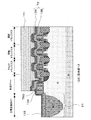
次に、図39(34)の画素部の断面図に示すように、光電変換部21上に導波路23形成してもよい。また、光電変換部21に入射光を集光するために、集光レンズ25を形成しても良い。
また、上記導波路23と集光レンズとの間に、光を分光するためのカラーフィルタ27を形成しても良い。
Next, as shown in the cross-sectional view of the pixel portion in FIG. 39 (34), a
Further, a
上記固体撮像装置の製造方法(第1例)では、サイドウォール形成膜と同一層の膜で形成された第1シリサイドブロック膜と、第1シリサイドブロック膜とは別の膜で形成された第2シリサイドブロック膜の2層で画素部12が被覆される。このため、画素部12のMOSトランジスタ上が1層のシリサイドブロック膜で完全に被覆されるのではないので、ランダムノイズが低減され、白傷・暗電流が低減される。 In the solid-state imaging device manufacturing method (first example), the first silicide block film formed of the same layer as the sidewall formation film and the second silicide block film formed of a film different from the first silicide block film are used. The pixel portion 12 is covered with two layers of silicide block films. For this reason, the MOS transistor of the pixel portion 12 is not completely covered with a single silicide block film, so that random noise is reduced and white scratches / dark currents are reduced.
上記製造方法では、前記図3、図4および図5(2)によって説明した固体撮像装置1(1B)が形成される。上記製造方法で、画素部12の転送ゲートTRG、リセットトランジスタRST、増幅トランジスタAmp、選択トランジスタSEL間の素子分離領域14を形成しない場合には、前記説明した固体撮像装置1(1A)が形成されることになる。この場合、フローティングディフュージョン部FDはリセットトランジスタRSTの一方の拡散層であるソース・ドレイン領域34と共通となる。
In the manufacturing method, the solid-state imaging device 1 (1B) described with reference to FIGS. 3, 4, and 5 (2) is formed. When the above-described manufacturing method does not form the
また、上記固体撮像装置およびその製造方法の説明では、1画素当たり一つの画素トランジスタ(例えば、リセットトランジスタ、増幅トランジスタ、選択トランジスタ)が形成されている構成で説明した。本発明は、1画素・1画素トランジスタの構成のみならず、2画素を一つの画素トランジスタで共有している構成の固体撮像装置、4画素を一つの画素トランジスタで共有している構成の固体撮像装置およびその製造方法にも同様に適用することができる。 In the description of the solid-state imaging device and the manufacturing method thereof, the description has been given of the configuration in which one pixel transistor (for example, a reset transistor, an amplification transistor, and a selection transistor) is formed per pixel. The present invention is not limited to the configuration of one pixel and one pixel transistor, but a solid-state imaging device having a configuration in which two pixels are shared by one pixel transistor, and a solid-state imaging having a configuration in which four pixels are shared by one pixel transistor. The present invention can be similarly applied to the apparatus and the manufacturing method thereof.
[固体撮像装置の製造方法の第2例]
例えば、一つの画素トランジスタが4画素を共有する構成の場合の製造方法の要部を説明する。
まず、一つの画素トランジスタが4画素を共有する構成の一例を、図40の平面レイアウト図によって説明する。
[Second Example of Manufacturing Method of Solid-State Imaging Device]
For example, the main part of the manufacturing method when one pixel transistor is configured to share four pixels will be described.
First, an example of a configuration in which one pixel transistor shares four pixels will be described with reference to a plan layout diagram of FIG.
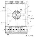
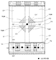
図40に示すように、4画素の各光電変換部21(21A、21B、21C、21D)が2行2列に配列されている。各光電変換部21の配列の中央には、各光電変換部21に連続するアクティブ領域にフローティングディフュージョン部FDが形成されている。また、各光電変換部21とフローティングディフュージョン部FDとの境界上にはゲート絶縁膜(図示せず)を介して転送ゲートTGG(TRG−A、TRG−B、TRG−C、TRG−D)がそれぞれに形成されている。上記各光電変換部21の周囲は、上記転送ゲートTRG下部の領域を除いて、拡散層からなる素子分離領域16によって電気的に分離されている。また、上記各光電変換部21に隣接した領域には、素子分離領域14を介して画素トランジスタ部17が形成されている。この画素トランジスタ部17は、例えば、リセットトランジスタRST、増幅トランジスタAmp、選択トランジスタSELが直列に配置されて構成されている。
As shown in FIG. 40, the four-pixel photoelectric conversion units 21 (21A, 21B, 21C, and 21D) are arranged in two rows and two columns. A floating diffusion portion FD is formed in the active region continuous to each
上記固体撮像装置の製造方法の第1例を、一つの画素トランジスタ部17を4画素で共有する固体撮像装置の製造方法に適用した場合の要部を以下に説明する。
画素トランジスタが4画素で共有される場合、前記第1例と異なるのは、光電変換部21の配列の中央にフローティングディフュージョン部FDが形成される点と、その各光電変換部21とフローティングディフュージョン部FDとの間上に転送ゲートTGGが形成される点である。
しかしながら、製造工程としては、光電変換部21、フローティングディフュージョン部FD、転送ゲートTGGの配置が異なるのみで、工程の作業内容は前記第1例と同一である。したがって、周辺回路部の製造方法は第1例と同じになる。以下、その一部を説明する。
The main part when the first example of the method for manufacturing a solid-state imaging device is applied to a method for manufacturing a solid-state imaging device in which one
When the pixel transistor is shared by four pixels, the difference from the first example is that the floating diffusion portion FD is formed at the center of the array of the
However, the manufacturing process is the same as that of the first example except that the
まず、サイドウォール形成工程について、図41の画素部の平面レイアウト図および図42(1)のB1−B1’線断面図、図42(2)のB2−B2’線断面図、図43(3)のB3−B3’線断面図、図43(4)のB4−B4’線断面図等を参照して説明する。サイドウォール形成膜137(第1シリサイドブロック膜71)を形成した後、サイドウォール形成膜137をエッチバックして、画素トランジスタ部17の各ゲート電極32、周辺回路部のゲート電極(図示せず)の各側壁にサイドウォール(図示せず)を形成する。その際、光電変換部21上はサイドウォール形成膜137が残される。これは、サイドウォールを形成する際のエッチングダメージが光電変換部21に入らないように、光電変換部21上をレジストマスク(図示せず)により被覆しておくためである。また、フローティングディフュージョン部FDが形成される領域上のサイドウォール形成膜137には開口部137Hが形成されていて、フローティングディフュージョン部FDの形成領域が露出されている。この開口部137Hの一部は転送ゲートTGR上にある。
First, regarding the sidewall formation step, a plan layout view of the pixel portion of FIG. 41, a cross-sectional view taken along line B1-B1 ′ of FIG. 42 (1), a cross-sectional view taken along line B2-B2 ′ of FIG. ) Along the B3-B3 ′ line, FIG. 43 (4) along the B4-B4 ′ line, and the like. After the sidewall formation film 137 (first silicide block film 71) is formed, the
その後、画素部や周辺回路部の各トランジスタのソース・ドレイン領域34、35が形成される。
Thereafter, source /
次に、次工程を、図44の画素部の平面レイアウト図および図45(1)のB1−B1’線断面図、図45(2)のB2−B2’線断面図、図46(3)のB3−B3’線断面図、図46(4)のB4−B4’線断面等を参照して説明する。画素部および周辺回路部の各トランジスタのソース・ドレイン領域が形成された後、周辺回路部のソース・ドレイン領域上等にシリサイド層を形成する。その際、画素トランジスタ、光電変換部21等にはシリサイド層を形成させないようにする必要がある。そこでシリサイド層を形成する前に、画素トランジスタ部17を被覆する第2シリサイドブロック膜72を形成する。その際、第2シリサイドブロック膜72は、素子分離領域14上で上記第1シリサイドブロック膜71にオーバーラップするように形成される。
このとき、フローティングディフュージョン部FD上も上記第1シリサイドブロック膜71の開口部137H周辺部にオーバーラップする状態に第2シリサイドブロック膜72が被覆される。
その後、前記第1例と同様に、周辺回路部のMOSトランジスタのソース・ドレイン領域上、ゲート電極上のシリサイド化工程以降の工程を行う。
Next, the next step is a plan layout view of the pixel portion of FIG. 44, a sectional view taken along line B1-B1 ′ of FIG. 45 (1), a sectional view taken along line B2-B2 ′ of FIG. 45 (2), and FIG. This will be described with reference to a cross-sectional view taken along line B3-B3 'of FIG. 46, a cross-section taken along line B4-B4' of FIG. After the source / drain regions of the transistors in the pixel portion and the peripheral circuit portion are formed, a silicide layer is formed on the source / drain regions of the peripheral circuit portion. At that time, it is necessary not to form a silicide layer in the pixel transistor, the
At this time, the second
Thereafter, similar to the first example, the steps after the silicidation step on the source / drain regions of the MOS transistor in the peripheral circuit portion and on the gate electrode are performed.
上記製造方法の第1例、第2例では、画素部12および周辺回路部13の各ゲート電極32、52の側壁にサイドウォール33、53を形成するとき、フローティングディフュージョン部FD上のサイドウォール形成膜137上はレジストマスクによって被覆されていない。この状態で、エッチングにより、各ゲート電極32、52の側壁にサイドウォール33、53を形成した場合、フローティングディフュージョン部FDにエッチングダメージを生じる懸念がある。
In the first and second examples of the manufacturing method, when the
上記エッチングダメージの懸念について、以下に説明する。
例えば、図47に示すように、エッチングにより、各ゲート電極(図示せず)の側壁にサイドウォール(図示せず)を形成した時、フローティングディフュージョン部FDにエッチングダメージを生じる可能性がる。
フローティングディフュージョン部FDにエッチングダメージが生じた場合、フローティングディフュージョン部FDの持つP/N接合にリークパスを発生させ、FD白傷を悪化させることになる。
The concern about the etching damage will be described below.
For example, as shown in FIG. 47, when sidewalls (not shown) are formed on the sidewalls of the gate electrodes (not shown) by etching, etching damage may occur in the floating diffusion portion FD.
When etching damage occurs in the floating diffusion portion FD, a leak path is generated in the P / N junction of the floating diffusion portion FD, and the FD white scratch is worsened.
ここで、FD白傷について説明する。光電変換部で光電変換した電子は、フローティングディフュージョン部FDに転送され電圧に変換される。この時、フローティングディフュージョン部FDにリークパスがあると、フローティングディフュージョン部FDに光電変換した電子がなくても、リークしてきた電子が出力されて白く見える。これをFD白傷と呼ぶ。 Here, FD white scratches will be described. The electrons photoelectrically converted by the photoelectric conversion unit are transferred to the floating diffusion unit FD and converted into a voltage. At this time, if there is a leak path in the floating diffusion part FD, even if there is no photoelectrically converted electron in the floating diffusion part FD, the leaked electrons are output and appear white. This is called FD white scratch.
また、光電変換部(図示せず)およびフローティングディフュージョン部FDの分離にP型拡散層からなる素子分離領域16を用いている場合がある。このように、画素間分離にP型拡散層を用いた場合に、特にFD白傷を大きく悪化させることになる。これは、例えば、ソース・ドレイン領域の活性化のため1000℃以上の熱処理時に、不純物の外方拡散の影響が考えられる。例えば、上記熱処理の際に外方拡散で飛散した不純物が、フローティングディフュージョン部FDとP型の拡散層からなる素子分離領域16の間に付着し、大きなリークパスを形成しFD白傷の発生の不具合を起す。
つまり、フローティングディフュージョン部FDへリーク電流が流れると、暗時(ダーク状態)であっても信号があるように見えるので、白傷が発生してしまう。
また、信号があるように見えるのは、フローティングディフュージョン部FDの電位をリセットした状態から信号電位を検出するまでの間に上記リークが発生すると、リセット電位にリーク電流による電圧変動分が重畳されるためである。
In some cases, the
That is, when a leak current flows to the floating diffusion portion FD, a signal appears to be present even in the dark (dark state), and white scratches occur.
In addition, when there is a leak between the reset of the potential of the floating diffusion portion FD and the detection of the signal potential, the signal appears to be present, and the voltage fluctuation due to the leak current is superimposed on the reset potential. Because.
上記一例では、一つの画素トランジスタが4画素を共有する構成の場合を示したが、2画素を共有する場合、1画素のみの場合も同様に、フローティングディフュージョン部FDにエッチングダメージを生じる可能性がある。 In the above example, a case in which one pixel transistor shares four pixels is shown. However, when two pixels are shared, there is a possibility that etching damage may occur in the floating diffusion portion FD in the case of only one pixel. is there.
<3.第3の実施の形態>
[固体撮像装置の構成の一例]
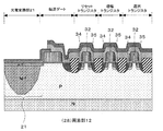
そこで、上記フローティングディフュージョン部FDにエッチングダメージを生じさせないようにする構成について、前記図1および図2、もしくは前記図3および図4によって説明した固体撮像装置1について説明する。
例えば、第1シリサイドブロック膜71は、光電変換部21上から、転送ゲートTGR上、フローティングディフュージョン部FD上、さらにリセットトランジスタRSTのゲート電極32の一部上を被覆するように形成される。この場合、第2シリサイドブロック膜72は、リセットトランジスタRSTのゲート電極32上で、第1シリサイドブロック膜71と重なるように形成される。
<3. Third Embodiment>
[Example of configuration of solid-state imaging device]
Therefore, a configuration for preventing etching damage from occurring in the floating diffusion portion FD will be described with reference to FIG. 1 and FIG. 2 or the solid-
For example, the first
上記第1、第2シリサイドブロック膜71、72を上記構成とすることで、サイドウォール33、周辺回路部のサイドウォール(図示せず)を形成するとき、フローティングディフュージョン部FD上もサイドウォール形成膜である第1シリサイドブロック膜71で被覆される。したがって、フローティングディフュージョン部FDにサイドウォール形成時のエッチングダメージが生じないようにすることができる。
By forming the first and second
[固体撮像装置の構成の第3例]
次に、前記図40で説明した一つの画素トランジスタで4画素を共有する構成の固体撮像装置についての第3例を説明する。以下、図48の画素部の平面レイアウト図および図49(1)のB1−B1’線断面図、図49(2)のC2−C2’線断面図、図50(3)のC3−C3’線断面図、図50(4)のC4−C4’線断面等を参照して説明する。
[Third example of configuration of solid-state imaging device]
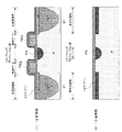
Next, a third example of a solid-state imaging device having a configuration in which four pixels are shared by one pixel transistor described with reference to FIG. 40 will be described. 48 is a plan layout view of the pixel portion in FIG. 48, a cross-sectional view taken along line B1-B1 ′ in FIG. 49 (1), a cross-sectional view taken along line C2-C2 ′ in FIG. Description will be made with reference to a cross-sectional view taken along a line, a cross section taken along line C4-C4 'of FIG.
第1シリサイドブロック膜71は、光電変換部21上から、転送ゲートTGR上、フローティングディフュージョン部FD上を被覆して形成されている。この場合、第2シリサイドブロック膜72は、第1シリサイドブロック膜71と例えば素子分離領域14上で重なるように、第1シリサイドブロック膜71が形成されていない画素トランジスタ部17を被覆して形成されている。
The first
したがって、画素トランジスタ部17のサイドウォール33、周辺回路部のサイドウォール(図示せず)を形成するとき、フローティングディフュージョン部FD上もサイドウォール形成膜である第1シリサイドブロック膜71で被覆される。このため、フローティングディフュージョン部FDにサイドウォール形成時のエッチングダメージが生じないようにすることができる。また、フローティングディフュージョン部FDが外方拡散の影響を受けないようにすることができる。これによりリークパスの発生を抑制し、FD白傷の発生を抑えることができるので、高画質は撮像が可能になる。
Therefore, when the
[固体撮像装置の構成の第4例]
次に、前記図40で説明した一つの画素トランジスタで4画素を共有する構成の固体撮像装置についての第4例を説明する。以下、図51の画素部の平面レイアウト図および図52(1)のD1−D1’線断面図、図52(2)のD2−D2’線断面図、図53(3)のD3−D3’線断面図、図53(4)のD4−D4’線断面等を参照して説明する。
[Fourth Example of Configuration of Solid-State Imaging Device]
Next, a fourth example of the solid-state imaging device having a configuration in which four pixels are shared by one pixel transistor described in FIG. 40 will be described. 51 is a plan layout view of the pixel portion in FIG. 51, a cross-sectional view taken along line D1-D1 ′ in FIG. 52 (1), a cross-sectional view taken along line D2-D2 ′ in FIG. 52 (2), and D3-D3 ′ in FIG. Description will be made with reference to a cross-sectional view taken along a line D4-D4 ′ of FIG. 53 (4), and the like.
第1シリサイドブロック膜71は、光電変換部21上から、転送ゲートTGR上、フローティングディフュージョン部FD上、さらにリセットトランジスタRSTのソース・ドレイン領域34上を被覆して形成されている。この場合、第2シリサイドブロック膜72は、第1シリサイドブロック膜71と例えば素子分離領域14とリセットトランジスタRSTのゲート電極32上で重なるように、第1シリサイドブロック膜71が形成されていない領域を被覆して形成されている。
The first
したがって、フローティングディフュージョン部FD上およびこのフローティングディフュージョン部FDに接続されるリセットトランジスタRSTのソース・ドレイン領域34上もサイドウォール形成膜である第1シリサイドブロック膜71で被覆される。したがって、画素トランジスタ部、周辺回路部(図示せず)にサイドウォールを形成する時、フローティングディフュージョン部FDおよびリセットトランジスタRSTのソース・ドレイン領域34にエッチングダメージが生じないようにすることができる。また、フローティングディフュージョン部FDおよびリセットトランジスタRSTのソース・ドレイン領域34が外方拡散の影響を受けないようにすることができる。これによりリークパスの発生を抑制し、FD白傷の発生を抑えることができるので、高画質は撮像が可能になる。
Therefore, the floating diffusion portion FD and the source /
なお、上記固体撮像装置の第3例、第4例ともに、周辺回路部の構成は前記図2、図4によって説明したのと同様になる。 In both the third and fourth examples of the solid-state imaging device, the configuration of the peripheral circuit unit is the same as that described with reference to FIGS.
<4.第4の実施の形態>
[固体撮像装置の製造方法の第3例]
次に、フローティングディフュージョン部FDのエッチングダメージを回避する製造方法(第3例)について、一つの画素トランジスタが4画素を共有する構成の場合の製造方法を一例にして、その要部を説明する。
<4. Fourth Embodiment>
[Third Example of Manufacturing Method of Solid-State Imaging Device]
Next, with respect to a manufacturing method (third example) for avoiding etching damage of the floating diffusion portion FD, an essential part thereof will be described by taking a manufacturing method in a case where one pixel transistor shares four pixels as an example.
画素トランジスタが4画素で共有される場合、前記第1例と異なるのは、光電変換部の配列の中央にフローティングディフュージョン部が形成される点と、その各光電変換部とフローティングディフュージョン部との間上に転送ゲートが形成される点である。
しかしながら、製造工程としては、光電変換部、フローティングディフュージョン部、転送ゲートの配置と、サイドウォール形成膜と第2シリサイドブロック膜のパターン形状が異なるのみで、工程の作業内容は前記第1例と同一である。以下、その一部を説明する。
When the pixel transistor is shared by four pixels, the difference from the first example is that a floating diffusion portion is formed at the center of the array of photoelectric conversion portions, and between each photoelectric conversion portion and the floating diffusion portion. The transfer gate is formed on the top.
However, the manufacturing process is the same as that of the first example except that the arrangement of the photoelectric conversion part, the floating diffusion part, the transfer gate, and the pattern shape of the sidewall formation film and the second silicide block film are different. It is. Some of these will be described below.
まず、サイドウォール形成工程について、図54の画素部の平面レイアウト図および図55(1)のC1−C1’線断面図、図55(2)のC2−C2’線断面図、図56(3)のC3−C3’線断面図、図56(4)のC4−C4’線断面図等を参照して説明する。サイドウォール形成膜137(第1シリサイドブロック膜71)を形成した後、サイドウォール形成膜137をエッチバックして、画素トランジスタ部17の各ゲート電極32、周辺回路部のゲート電極(図示せず)の各側壁にサイドウォール(図示せず)を形成する。その際、光電変換部21上およびフローティングディフュージョン部FD上(転送ゲートTRG上も含む)はサイドウォール形成膜137が残される。これは、サイドウォールを形成する際のエッチングダメージが光電変換部21およびフローティングディフュージョン部FDに入らないように、光電変換部21上およびフローティングディフュージョン部FD上をレジストマスク(図示せず)により被覆しておくためである。
すなわち、前記説明した製造方法の第1例において、レジストマスク138(前記図25参照)をフローティングディフュージョン部FDまで延長して形成する点が異なるのみで、ここまでのその他の工程は第1例と同様な工程となる。
なお、上記フローティングディフュージョン部FD、ソース・ドレイン領域34等は、この段階では、まだ形成されていない。図面上、位置関係をわかりやすくするために、フローティングディフュージョン部FD、ソース・ドレイン領域34を記載したものである。
First, regarding the sidewall formation step, a plan layout view of the pixel portion in FIG. 54, a cross-sectional view taken along line C1-C1 ′ in FIG. 55 (1), a cross-sectional view taken along line C2-C2 ′ in FIG. ), A cross-sectional view taken along line C3-C3 ′, a cross-sectional view taken along line C4-C4 ′ of FIG. 56 (4), and the like. After the sidewall formation film 137 (first silicide block film 71) is formed, the
That is, the first example of the manufacturing method described above is different from the first example only in that the resist mask 138 (see FIG. 25) is formed to extend to the floating diffusion portion FD. The same process is performed.
Note that the floating diffusion portion FD, the source /
その後、画素部や周辺回路部の各トランジスタのソース・ドレイン領域34、35が形成される。その際、フローティングディフュージョンFD上はサイドウォール形成膜137に被覆されているため、画素部や周辺回路部の各トランジスタのソース・ドレイン領域を形成するイオン注入とは別途にイオン注入を行うことが望ましい。
Thereafter, source /
次に、次工程を、図57の画素部の平面レイアウト図および図58(1)のC1−C1’線断面図、図58(2)のC2−C2’線断面図、図59(3)のC3−C3’線断面図、図59(4)のC4−C4’線断面等を参照して説明する。
画素部12および周辺回路部(図示せず)の各トランジスタのソース・ドレイン領域が形成された後、周辺回路部のソース・ドレイン領域上等にシリサイド層を形成する。その際、画素トランジスタ部17、光電変換部21等にはシリサイド層を形成させないようにする必要がある。そこでシリサイド層を形成する前に、画素トランジスタ部17を被覆する第2シリサイドブロック膜72を形成する。その際、第2シリサイドブロック膜72は、上記第1シリサイドブロック膜71にオーバーラップするように形成される。また、その他の部分では、素子分離領域14上で第1シリサイドブロック膜71とオーバーラップさせればよい。
その後、前記第1例と同様に、周辺回路部のMOSトランジスタのソース・ドレイン領域上、ゲート電極上のシリサイド化工程以降の工程を行う。
Next, the next step is a plan layout view of the pixel portion of FIG. 57, a sectional view taken along line C1-C1 ′ of FIG. 58 (1), a sectional view taken along line C2-C2 ′ of FIG. 58 (2), and FIG. This will be described with reference to a cross-sectional view taken along line C3-C3 ′ of FIG.
After the source / drain regions of the transistors in the pixel portion 12 and the peripheral circuit portion (not shown) are formed, a silicide layer is formed on the source / drain regions of the peripheral circuit portion. At this time, it is necessary not to form a silicide layer in the
Thereafter, similar to the first example, the steps after the silicidation step on the source / drain regions of the MOS transistor in the peripheral circuit portion and on the gate electrode are performed.
したがって、画素トランジスタ部17のサイドウォール33、周辺回路部のサイドウォール(図示せず)を形成するとき、フローティングディフュージョン部FD上もサイドウォール形成膜である第1シリサイドブロック膜71で被覆される。このため、フローティングディフュージョン部FDにサイドウォール形成時のエッチングダメージが生じないようにすることができる。また、フローティングディフュージョン部FDが外方拡散の影響を受けないようにすることができる。これによりリークパスの発生を抑制し、FD白傷の発生を抑えることができるので、高画質は撮像が可能な固体撮像装置を製造することが可能になる。さらにシリサイド層を形成する前に画素トランジスタ部17を第2シリサイドブロック膜72で被覆することができる。
Therefore, when the
[固体撮像装置の製造方法の第4例]
次に、フローティングディフュージョン部FDのエッチングダメージを回避する製造方法(第4例)について、一つの画素トランジスタが4画素を共有する構成の場合の製造方法を一例にして、その要部を説明する。
[Fourth Example of Manufacturing Method of Solid-State Imaging Device]
Next, with respect to a manufacturing method (fourth example) for avoiding etching damage of the floating diffusion portion FD, the main part will be described by taking as an example a manufacturing method in a case where one pixel transistor shares four pixels.
画素トランジスタが4画素で共有される場合、前記第1例と異なるのは、光電変換部の配列の中央にフローティングディフュージョン部が形成される点と、その各光電変換部とフローティングディフュージョン部との間上に転送ゲートが形成される点である。
しかしながら、製造工程としては、光電変換部、フローティングディフュージョン部、転送ゲートの配置と、サイドウォール形成膜と第2シリサイドブロック膜のパターン形状が異なるのみで、工程の作業内容は前記第1例と同一である。以下、その一部を説明する。
When the pixel transistor is shared by four pixels, the difference from the first example is that a floating diffusion portion is formed at the center of the array of photoelectric conversion portions, and between each photoelectric conversion portion and the floating diffusion portion. The transfer gate is formed on the top.
However, the manufacturing process is the same as that of the first example except that the arrangement of the photoelectric conversion part, the floating diffusion part, the transfer gate, and the pattern shape of the sidewall formation film and the second silicide block film are different. It is. Some of these will be described below.
まず、サイドウォール形成工程について、図60の画素部の平面レイアウト図および図61(1)のD1−D1’線断面図、図61(2)のD2−D2’線断面図、図62(3)のD3−D3’線断面図、図62(4)のD4−D4’線断面図等を参照して説明する。
サイドウォール形成膜137(第1シリサイドブロック膜71)を形成した後、サイドウォール形成膜137をエッチバックして、画素トランジスタ部17の各ゲート電極32、周辺回路部のゲート電極(図示せず)の各側壁にサイドウォール(図示せず)を形成する。その際、光電変換部21上、フローティングディフュージョン部FD上(転送ゲートTRG上も含む)およびリセットトランジスタRSTのソース・ドレイン領域34上はサイドウォール形成膜137が残される。これは、サイドウォールを形成する際のエッチングダメージが、光電変換部21、フローティングディフュージョン部FD(転送ゲートTRG上も含む)およびリセットトランジスタRSTのソース・ドレイン領域34に入らないように、光電変換部21上、フローティングディフュージョン部FD上、およびリセットトランジスタRSTのソース・ドレイン領域34上をレジストマスク(図示せず)により被覆しておくためである。
すなわち、前記説明した製造方法の第1例において、レジストマスク138(前記図25参照)をフローティングディフュージョン部FDおよびリセットトランジスタRSTのソース・ドレイン領域34、さらにリセットトランジスタRSTのゲート電極32の一部上まで延長して形成する点が異なるのみで、ここまでのその他の工程は第1例と同様な工程となる。
なお、上記フローティングディフュージョン部FD、ソース・ドレイン領域34等は、この段階では、まだ形成されていない。図面上、位置関係をわかりやすくするために、フローティングディフュージョン部FD、ソース・ドレイン領域34を記載したものである。
First, regarding the sidewall formation step, a plan layout view of the pixel portion of FIG. 60, a cross-sectional view taken along line D1-D1 ′ of FIG. 61 (1), a cross-sectional view taken along line D2-D2 ′ of FIG. ), A cross-sectional view taken along line D3-D3 ′, a cross-sectional view taken along line D4-D4 ′ of FIG.
After the sidewall formation film 137 (first silicide block film 71) is formed, the
That is, in the first example of the manufacturing method described above, the resist mask 138 (see FIG. 25) is placed on the floating diffusion portion FD, the source /
Note that the floating diffusion portion FD, the source /
その後、画素部や周辺回路部の各トランジスタのソース・ドレイン領域34、35が形成される。その際、フローティングディフュージョンFDおよびリセットトランジスタRSTのソース・ドレイン領域34上はサイドウォール形成膜137に被覆されているため、画素部や周辺回路部の各トランジスタのソース・ドレイン領域を形成するイオン注入とは別途にイオン注入を行うことが望ましい。
Thereafter, source /
次に、次工程を、図63の画素部の平面レイアウト図および図64(1)のD1−D1’線断面図、図64(2)のD2−D2’線断面図、図65(3)のD3−D3’線断面図、図65(4)のD4−D4’線断面等を参照して説明する。
画素部および周辺回路部の各トランジスタのソース・ドレイン領域が形成された後、周辺回路部のソース・ドレイン領域上等にシリサイド層を形成する。その際、画素トランジスタ部17、光電変換部21等にはシリサイド層を形成させないようにする必要がある。そこでシリサイド層を形成する前に、画素トランジスタ部17を被覆する第2シリサイドブロック膜72を形成する。その際、第2シリサイドブロック膜72は、上記第1シリサイドブロック膜71にオーバーラップするように形成される。このとき、リセットトランジスタRSTのゲート電極32の一部上まで第1シリサイドブロック膜71が形成されているので、第2シリサイドブロック膜72はリセットトランジスタRSTのゲート電極32上で第1シリサイドブロック膜71とオーバーラップさせればよい。また、その他の部分では、素子分離領域14上で第1シリサイドブロック膜71とオーバーラップさせればよい。
その後、前記第1例と同様に、周辺回路部のMOSトランジスタのソース・ドレイン領域上、ゲート電極上のシリサイド化工程以降の工程を行う。
Next, the next step is a plan layout view of the pixel portion of FIG. 63, a sectional view taken along line D1-D1 ′ of FIG. 64 (1), a sectional view taken along line D2-D2 ′ of FIG. 64 (2), and FIG. This will be described with reference to a cross-sectional view taken along line D3-D3 'of FIG. 65, a cross-section taken along line D4-D4' of FIG.
After the source / drain regions of the transistors in the pixel portion and the peripheral circuit portion are formed, a silicide layer is formed on the source / drain regions of the peripheral circuit portion. At this time, it is necessary not to form a silicide layer in the
Thereafter, similar to the first example, the steps after the silicidation step on the source / drain regions of the MOS transistor in the peripheral circuit portion and on the gate electrode are performed.
したがって、画素トランジスタ部17のサイドウォール33、周辺回路部のサイドウォール(図示せず)を形成するとき、フローティングディフュージョン部FD上もサイドウォール形成膜である第1シリサイドブロック膜71で被覆される。このため、フローティングディフュージョン部FDにサイドウォール形成時のエッチングダメージが生じないようにすることができる。また、フローティングディフュージョン部FDが外方拡散の影響を受けないようにすることができる。これによりリークパスの発生を抑制し、FD白傷の発生を抑えることができるので、高画質は撮像が可能な固体撮像装置を製造することが可能になる。さらにシリサイド層を形成する前に画素トランジスタ部17を第2シリサイドブロック膜72で被覆することができる。
Therefore, when the
[固体撮像装置およびその製造方法の第3、第4例の変形例]
上記第3例、第4例の4画素を一つの画素トランジスタ部17で共有する構成では、光電変換部21周囲の素子分離は拡散層(P+型拡散層)分離であり、画素トランジスタ部17周囲の素子分離はSTI(Shallow Trench Isolation)構造の素子分離を用いた。例えば、図66に示すように、光電変換部21周囲の素子分離および画素トランジスタ部17周囲の素子分離を拡散層(P+型拡散層)からなる素子分離領域16で形成することもできる。
この場合、前記第1シリサイドブロック膜71は、前記第3例、第4例等で説明したのと同様に形成することができる。また前記第2シリサイドブロック膜72は、前記第3例、第4例等で説明したのと同様に形成することができる。
[Modifications of Third and Fourth Examples of Solid-State Imaging Device and Manufacturing Method Thereof]
In the configuration in which the four pixels in the third and fourth examples are shared by one
In this case, the first
[固体撮像装置およびその製造方法の第1例の変形例]
また、前記図5(1)に示した構成では、光電変換部21、画素トランジスタ部周囲の素子分離はSTI(Shallow Trench Isolation)構造の素子分離を用いた。例えば、図67〜図69に示すように、光電変換部21周囲の素子分離および画素トランジスタ部17周囲の素子分離を拡散層(P+型拡散層)からなる素子分離領域16で形成することもできる。
この場合、前記第1シリサイドブロック膜71は、光電変換部21上、転送ゲートTRG上、フローティングディフュージョン部FD上、リセットトランジスタRSTのソース・ドレイン領域34上を被覆し、さらにリセットトランジスタRSTのゲート電極32の一部上を被覆するように形成される。また前記第2シリサイドブロック膜72は、上記第1シリサイドブロック膜71にオーバーラップするように形成される。このとき、リセットトランジスタRSTのゲート電極32の一部上まで第1シリサイドブロック膜71が形成されているので、第2シリサイドブロック膜72はリセットトランジスタRSTのゲート電極32上で第1シリサイドブロック膜71とオーバーラップさせればよい。また、その他の部分では、素子分離領域16上で第1シリサイドブロック膜71とオーバーラップさせればよい。
なお、図68は図67中のA−A’線断面図であり、図69は図67中のE−E’線断面図である。
[Modification of First Example of Solid-State Imaging Device and Manufacturing Method Thereof]
In the configuration shown in FIG. 5A, the element isolation around the
In this case, the first
68 is a cross-sectional view taken along line AA ′ in FIG. 67, and FIG. 69 is a cross-sectional view taken along line EE ′ in FIG.
なお、上記固体撮像装置の製造方法の第3例、第4例ともに、周辺回路部の構成は前記製造方法の第1例と同様になる。 In both the third and fourth examples of the method for manufacturing the solid-state imaging device, the configuration of the peripheral circuit unit is the same as that of the first example of the manufacturing method.
[固体撮像装置の製造方法の詳細例]
次に、一つの画素トランジスタが4画素を共有する構成の場合の製造方法の一詳細例を図70〜図93の製造工程断面図によって説明する。この製造方法は、前記図51の画素部の平面レイアウト図によって説明した構成を形成する製造方法である。
また、それぞれの図面の(1)にD1−D1’線位置に相当する断面図、(2)のD2−D2’線位置に相当する断面図、(3)のD3−D3’線位置に相当する断面図、(4)のD4−D4’線位置に相当する断面図を示す。
[Detailed example of manufacturing method of solid-state imaging device]
Next, a detailed example of a manufacturing method in a case where one pixel transistor shares four pixels will be described with reference to manufacturing process cross-sectional views of FIGS. This manufacturing method is a manufacturing method for forming the configuration described with reference to the plan layout diagram of the pixel portion of FIG.
Also, (1) in each drawing is a cross-sectional view corresponding to the D1-D1 ′ line position, (2) is a cross-sectional view corresponding to the D2-D2 ′ line position, and (3) is equivalent to a D3-D3 ′ line position. Sectional drawing to perform and sectional drawing equivalent to the D4-D4 'line position of (4) are shown.
まず、前記図6〜図12によって説明した工程を行う。
半導体基板11には例えばシリコン基板を用いる。そして、画素トランジスタの周辺に素子分離領域14を形成し、周辺回路部13の第2素子分離領域15を形成する。
次に、前記図6〜図12には図示していないが、半導体基板11にpウエル、nウエルを形成する。さらに、チャネルイオン注入を行う。さらに、光電変換部にフォトダイオードを形成するイオン注入を行い、p型領域を形成する。例えば、光電変換部が形成される半導体基板の表面には、ホウ素(B)のイオン注入を行い、深い領域にヒ素(As)もしくはリン(P)を用いてイオン注入を行い、上記p型領域の下部に接合するn型領域を形成する。このようにして、pn接合の光電変換部を形成する。
First, the steps described with reference to FIGS.
For example, a silicon substrate is used as the
Next, although not shown in FIGS. 6 to 12, ap well and n well are formed in the
次に、図70(1)のD1−D1’線位置に相当する断面図、図70(2)のD2−D2’線位置に相当する断面図、図71(3)のD3−D3’線位置に相当する断面図、図71(4)のD4−D4’線位置に相当する断面等を参照して説明する。
半導体基板11上に犠牲酸化膜151を形成する。次いで、上記犠牲酸化膜151上に、レジストマスク152を形成する。このレジストマスク152は、上記光電変換部21の周囲に形成される素子分離領域上に開口部153が設けられている。つまり、レジストマスク152によって、光電変換部21上、および転送ゲート、フローティングディフュージョン部、画素トランジスタの各形成領域上が被覆される。
次いで、上記レジストマスク152をイオン注入マスクに用いて、上記半導体基板11にイオン注入を行い、P+型の素子分離領域16を形成する。このイオン注入は、例えばイオン種にホウ素(B)を用い、ドーズ量を1×10¹²/cm2〜1×1013/cm2に設定する。また、注入エネルギーを10keV〜30keVに設定する。また、深さに応じてイオン注入を多段階に行ってもよい。
これによって、各光電変換部21は、素子分離領域16で分離され、リセットトランジスタ、増幅トランジスタ、選択トランジスタ等が形成される画素トランジスタの形成領域とは素子分離領域14によって分離される。また、図示はしていないが、周辺回路部は、前記説明したように、素子分離領域(15)によって分離されている。
Next, a cross-sectional view corresponding to the D1-D1 ′ line position in FIG. 70 (1), a cross-sectional view corresponding to the D2-D2 ′ line position in FIG. 70 (2), and the D3-D3 ′ line in FIG. Description will be made with reference to a cross-sectional view corresponding to the position, a cross-section corresponding to the position of the line D4-D4 'in FIG.
A
Next, using the resist
Thus, each
その後、上記レジストマスク152を除去し、さらに上記犠牲酸化膜151を除去する。図面は、レジストマスク152を除去する直前の状態を示した。
Thereafter, the resist
次に、図72(1)のD1−D1’線位置に相当する断面図、図72(2)のD2−D2’線位置に相当する断面図、図73(3)のD3−D3’線位置に相当する断面図、図73(4)のD4−D4’線位置に相当する断面等を参照して説明する。
図72および図73に示すように、半導体基板11上にゲート絶縁膜31を形成し、さらにゲート絶縁膜31上にゲート電極形成膜131を形成する。このとき、図示はしていないが、前記図14に示すように、周辺回路部13の半導体基板11上にもゲート絶縁膜51を形成し、ゲート絶縁膜51上に上記ゲート電極形成膜131を形成する。
上記ゲート電極形成膜131は、例えばLP−CVD法により、ポリシリコンを堆積して形成する。堆積膜厚は、技術ノードにもよるが、90nmノードでは、150nm〜200nmとする。
また、膜厚は、加工の制御性から一般にゲートアスペクト比を大きくしないため、ノード毎に薄くなる傾向にある。
そして、ゲート空乏化対策として、ポリシリコンの代わりにシリコンゲルマニウム(SiGe)を用いてよい。このゲート空乏化とは、ゲート酸化膜の膜厚が薄膜化するに伴い、物理的なゲート酸化膜の膜厚だけでなくゲートポリシリコン内の空乏層の膜厚の影響が無視できなくなって、実効的なゲート酸化膜の膜厚が薄くならず、トランジスタ性能が落ちてしまうという問題である。
Next, a cross-sectional view corresponding to the D1-D1 ′ line position in FIG. 72 (1), a cross-sectional view corresponding to the D2-D2 ′ line position in FIG. 72 (2), and the D3-D3 ′ line in FIG. 73 (3). Description will be made with reference to a cross-sectional view corresponding to a position, a cross-section corresponding to a position along line D4-D4 ′ in FIG.
As shown in FIGS. 72 and 73, a
The gate
In addition, the film thickness tends to become thinner at each node because the gate aspect ratio is generally not increased from the controllability of processing.
As a gate depletion countermeasure, silicon germanium (SiGe) may be used instead of polysilicon. This gate depletion means that as the thickness of the gate oxide film becomes thinner, not only the physical gate oxide film thickness but also the influence of the thickness of the depletion layer in the gate polysilicon cannot be ignored. This is a problem that the effective gate oxide film thickness is not reduced and the transistor performance is degraded.
次に、図74(1)のD1−D1’線位置に相当する断面図、図74(2)のD2−D2’線位置に相当する断面図、図75(3)のD3−D3’線位置に相当する断面図、図75(4)のD4−D4’線位置に相当する断面等を参照して説明する。
図74および図75に示すように、ゲート空乏化対策を行う。まず、周辺回路部13のpMOSトランジスタの形成領域上にレジストマスク132を形成(前記図16参照)し、nMOSトランジスタの形成領域の上記ゲート電極形成膜131にn型不純物をドーピングする。このドーピングは、例えばリン(P)またはヒ素(As)をイオン注入して行う。イオン注入量は、約1×10¹⁵/cm2〜1×1016/cm2である。その後、上記レジストマスク132を除去する。
次いで、図示はしていないが、nMOSトランジスタの形成領域上にレジストマスク(図示せず)を形成し、周辺回路部13(前記図16参照)のpMOSトランジスタの形成領域の上記ゲート電極形成膜131にp型不純物をドーピングする。このドーピングは、例えばホウ素(B)または二フッ化ホウ素(BF2)またはインジウム(In)をイオン注入して行う。イオン注入量は、約1×10¹⁵/cm2〜1×1016/cm2である。その後、上記レジストマスクを除去する。
上記イオン注入は、どちらを先に行ってもよい。
また、上記各イオン注入において、イオン注入した不純物がゲート絶縁膜の直下に突き抜けるのを防ぐために、窒素(N2)のイオン注入を組み合わせても良い。
Next, a cross-sectional view corresponding to the D1-D1 ′ line position in FIG. 74 (1), a cross-sectional view corresponding to the D2-D2 ′ line position in FIG. 74 (2), and the D3-D3 ′ line in FIG. Description will be made with reference to a cross-sectional view corresponding to the position, a cross-section corresponding to the position of the line D4-D4 'in FIG.
As shown in FIGS. 74 and 75, gate depletion countermeasures are taken. First, a resist
Next, although not shown, a resist mask (not shown) is formed on the nMOS transistor formation region, and the gate
Either of the ion implantations may be performed first.
Further, in each of the above ion implantations, nitrogen (N 2 ) ion implantation may be combined in order to prevent the implanted ions from penetrating directly under the gate insulating film.
次に、図76(1)のD1−D1’線位置に相当する断面図、図76(2)のD2−D2’線位置に相当する断面図、図77(3)のD3−D3’線位置に相当する断面図、図77(4)のD4−D4’線位置に相当する断面等を参照して説明する。
図76および図77に示すように、上記ゲート電極形成膜131上に各ゲート電極を形成するためのレジストマスク(図示せず)を形成する。このレジストマスクをエッチングマスクに用いた反応性イオンエッチングによって、上記ゲート電極形成膜131上をエッチング加工して画素部12の各MOSトランジスタのゲート電極32、転送ゲートTRG、周辺回路部13の各MOSトランジスタのゲート電極52を形成(前記図18参照)する。
次いで、上記各ゲート電極32、ゲート電極52(前記図18参照)の表面を酸化して酸化膜133を形成する。
上記酸化膜133の膜厚は、例えば1nm〜10nmとする。また、上記酸化膜133は、上記ゲート電極32、52の側壁とともに上面にも形成されている。
さらに、上記酸化工程によって、上記ゲート電極32、52のエッジ部分を丸めることによって、酸化膜耐圧を改善することができる効果がある。
また、上記熱処理が行われることによって、エッチダメージを低減することができる。
また、上記ゲート電極加工において、光電変換部21上に形成されていた上記ゲート絶縁膜が除去されたとしても、光電変換部21上にも上記酸化膜133が形成される。このため、次工程のリソグラフィー技術においてレジスト膜を形成した際に、シリコン表面に直付けではなくなるために、このレジストによる汚染を防止できる。よって、画素部12の光電変換部21にとっては、白傷防止対策になる。
Next, a sectional view corresponding to the D1-D1 ′ line position in FIG. 76 (1), a sectional view corresponding to the D2-D2 ′ line position in FIG. 76 (2), and a D3-D3 ′ line in FIG. 77 (3). Description will be made with reference to a cross-sectional view corresponding to a position, a cross-section corresponding to a position along line D4-D4 'in FIG. 77 (4), and the like.
As shown in FIGS. 76 and 77, a resist mask (not shown) for forming each gate electrode is formed on the gate
Next, the surfaces of the
The film thickness of the
Furthermore, the oxide film withstand voltage can be improved by rounding the edge portions of the
Further, etch damage can be reduced by performing the heat treatment.
In the gate electrode processing, even if the gate insulating film formed on the
次に、図78(1)のD1−D1’線位置に相当する断面図、図78(2)のD2−D2’線位置に相当する断面図、図79(3)のD3−D3’線位置に相当する断面図、図79(4)のD4−D4’線位置に相当する断面等を参照して説明する。
図78および図79に示すように、画素部12の各MOSトランジスタのLDD領域38、39等を形成するとともに、周辺回路部13の各MOSトランジスタのLDD領域61、62、63、64等を形成(前記図20参照)する。
Next, a cross-sectional view corresponding to the D1-D1 ′ line position in FIG. 78 (1), a cross-sectional view corresponding to the D2-D2 ′ line position in FIG. 78 (2), and the D3-D3 ′ line in FIG. 79 (3). Description will be made with reference to a cross-sectional view corresponding to the position, a cross section corresponding to the position of the line D4-D4 'in FIG.
As shown in FIGS. 78 and 79, the
まず、周辺回路部13に形成されるNMOSトランジスタに関しては、各ゲート電極52(52N)の両側における半導体基板11にポケット拡散層65、66を形成(前記図20参照)する。このポケット拡散層65、66は、イオン注入により形成され、イオン注入種に例えば二フッ化ホウ素(BF2)またはホウ素(B)またはインジウム(In)を用い、ドーズ量を例えば1×10¹²/cm2〜1×1014/cm2に設定する。
さらに各ゲート電極52(52N)の両側における半導体基板11にLDD領域61、62を形成する。LDD領域61、62は、イオン注入により形成され、イオン注入種に例えばヒ素(As)もしくはリン(P)を用い、ドーズ量を例えば1×10¹³/cm2〜1×1015/cm2に設定する。
First, for the NMOS transistor formed in the peripheral circuit section 13, pocket diffusion layers 65 and 66 are formed in the
Further,
上記画素部12に形成されるMOSトランジスタに関しては、各ゲート電極32の両側における半導体基板11にLDD領域38、39を形成する。LDD領域38、39は、イオン注入により形成され、イオン注入種に例えばヒ素(As)もしくはリン(P)を用い、ドーズ量を例えば1×10¹³/cm2〜1×1015/cm2に設定する。また、ポケット拡散層を形成してもよい。
上記画素部12に形成されるMOSトランジスタに関しては、工程削減の観点から、LDD領域を形成しなくてもよい。もしくは、周辺回路部13に形成されるMOSトランジスタのLDDイオン注入と兼ねてもよい。
With respect to the MOS transistor formed in the pixel portion 12,
With respect to the MOS transistor formed in the pixel portion 12, the LDD region may not be formed from the viewpoint of process reduction. Alternatively, it may also serve as LDD ion implantation of a MOS transistor formed in the peripheral circuit section 13.
周辺回路部13のPMOSトランジスタの形成領域に関しては、各ゲート電極52の両側における半導体基板11にポケット拡散層67、68を形成(前記図20参照)する。このポケット拡散層67、68は、イオン注入により形成され、イオン注入種に例えばヒ素(As)またはリン(P)を用い、ドーズ量を例えば1×10¹²/cm2〜1×1014/cm2に設定する。
さらに各ゲート電極52(52P)の両側における半導体基板11にLDD領域63、64を形成する。LDD領域63、64は、イオン注入により形成され、イオン注入種に例えば二フッ化ホウ素(BF2)またはホウ素(B)またはインジウム(In)を用い、ドーズ量を例えば1×10¹³/cm2〜1×1015/cm2に設定する。
Regarding the formation region of the PMOS transistor in the peripheral circuit portion 13, pocket diffusion layers 67 and 68 are formed in the
Further,
また、周辺回路部のNMOSトランジスタ、PMOSトランジスタのポケットイオン注入前に、注入のチャネリング抑制技術として、ゲルマニウム(Ge)をイオン注入することなどでプリアモルファス化を行ってもよい。また、LDD領域形成後、TED(Transient Enhanced Diffusion)などを引き起こす注入欠陥を小さくするために、800℃〜900℃程度のRTA(Rapid Thermal Annealing)処理を追加してもよい。 Further, pre-amorphization may be performed by implanting germanium (Ge) as a channeling suppression technique for implantation before pocket ion implantation of the NMOS transistor and PMOS transistor in the peripheral circuit portion. Further, after the formation of the LDD region, an RTA (Rapid Thermal Annealing) process of about 800 ° C. to 900 ° C. may be added in order to reduce implantation defects that cause TED (Transient Enhanced Diffusion) or the like.
次に、図80(1)のD1−D1’線位置に相当する断面図、図80(2)のD2−D2’線位置に相当する断面図、図81(3)のD3−D3’線位置に相当する断面図、図81(4)のD4−D4’線位置に相当する断面等を参照して説明する。
図80および図81に示すように、画素部12および周辺回路部13(前記図22参照)の全面に酸化シリコン(SiO2)膜134を形成する。この酸化シリコン膜134は、ノンドープトシリケートガラス(NSG)またはLP−TEOS(Tetra Ethyl Ortho Silicate)または高温酸化(HTO)膜等の堆積膜で形成される。上記酸化シリコン膜134は、例えば5nm〜20nmの膜厚に形成される。
次に、上記酸化シリコン膜134上に窒化シリコン膜135を形成する。この窒化シリコン膜135は、例えばLPCVDにて形成された窒化シリコン膜を用いる。その膜厚は、例えば10nm〜100nmとする。
上記窒化シリコン膜135は、低温で成膜できる原子層蒸着法により成膜されたALD窒化シリコン膜でもよい。
上記窒化シリコン膜135の直下の上記酸化シリコン膜134は、画素部12の光電変換部21上では、その膜厚が薄いほど、光反射を防ぐので、光電変換部21の感度が良くなる。
次に、必要に応じて、上記窒化シリコン膜135上に3層目の酸化シリコン(SiO2)膜136を堆積する。この酸化シリコン膜136は、NSGまたはLP−TEOSまたはHTO等の堆積膜で形成される。この酸化シリコン膜136は、例えば10nm〜100nmの膜厚に形成される。
Next, a cross-sectional view corresponding to the D1-D1 ′ line position in FIG. 80 (1), a cross-sectional view corresponding to the D2-D2 ′ line position in FIG. 80 (2), and the D3-D3 ′ line in FIG. Description will be made with reference to a cross-sectional view corresponding to a position, a cross-section corresponding to a position along line D4-D4 ′ in FIG.
As shown in FIGS. 80 and 81, a silicon oxide (SiO 2 )
Next, a
The
Since the
Next, a third silicon oxide (SiO 2 )
したがって、サイドウォール形成膜137は、酸化シリコン膜136/窒化シリコン膜135/酸化シリコン膜134の3層構造膜となる。なお、このサイドウォール形成膜137は、窒化シリコン膜/酸化シリコン膜の2層構造膜であってもよい。以下、3層構造膜のサイドウォール形成膜137で説明する。
Therefore, the
次に、図82(1)のD1−D1’線位置に相当する断面図、図82(2)のD2−D2’線位置に相当する断面図、図83(3)のD3−D3’線位置に相当する断面図、図83(4)のD4−D4’線位置に相当する断面等を参照して説明する。
図82および図83に示すように、最上層に形成されている上記酸化シリコン膜136をエッチバックして、各ゲート電極32、52(前記図24参照)、転送ゲートTRG等の側部側にのみ残す。上記エッチバックは、例えば反応性イオンエッチング(RIE)によって行う。このエッチバックでは、上記窒化シリコン膜135でエッチングを停止する。このように、窒化シリコン膜135でエッチングを停止するため、画素部12の光電変換部21へのエッチダメージを低減することができるので、白傷を低減することができる。
Next, a cross-sectional view corresponding to the D1-D1 ′ line position in FIG. 82 (1), a cross-sectional view corresponding to the D2-D2 ′ line position in FIG. 82 (2), and the D3-D3 ′ line in FIG. 83 (3). Description will be made with reference to a cross-sectional view corresponding to the position, a cross-section corresponding to the position of the line D4-D4 'in FIG.
As shown in FIGS. 82 and 83, the
次に、図84(1)のD1−D1’線位置に相当する断面図、図84(2)のD2−D2’線位置に相当する断面図、図85(3)のD3−D3’線位置に相当する断面図、図85(4)のD4−D4’線位置に相当する断面等を参照して説明する。
図84および図85に示すように、画素部12の光電変換部21上の全面、転送ゲートTRG上、フローティングディフュージョン部が形成される領域上、リセットトランジスタのLDD領域38上およびリセットトランジスタのゲート電極32上の一部にかかるように、レジストマスク138を形成する。
その後、上記窒化シリコン膜135、上記酸化シリコン膜134をエッチバックして、各ゲート電極32、52(前記図26参照)の側壁部に酸化シリコン膜134、窒化シリコン膜135、酸化シリコン膜136からなる第1サイドウォール33、第2サイドウォール53(前記図26参照)を形成する。このとき、光電変換部21上、フローティングディフュージョン部を形成する領域上、リセットトランジスタのソース・ドレイン領域を形成する領域上の窒化シリコン膜135、酸化シリコン膜134は、レジストマスク138で被覆されているので、エッチングされない。したがって、光電変換部21、フローティングディフュージョン部を形成する領域、リセットトランジスタのソース・ドレイン領域を形成する領域にエッチングダメージが生じることはない。
Next, a cross-sectional view corresponding to the D1-D1 ′ line position in FIG. 84 (1), a cross-sectional view corresponding to the D2-D2 ′ line position in FIG. 84 (2), and the D3-D3 ′ line in FIG. Description will be made with reference to a cross-sectional view corresponding to the position, a cross-section corresponding to the position of the line D4-D4 'in FIG.
As shown in FIGS. 84 and 85, the entire surface of the pixel portion 12 on the
Thereafter, the
次に、図86(1)のD1−D1’線位置に相当する断面図、図86(2)のD2−D2’線位置に相当する断面図、図87(3)のD3−D3’線位置に相当する断面図、図87(4)のD4−D4’線位置に相当する断面等を参照して説明する。
まず、前記図28に示すように、周辺回路部13のNMOSトランジスタの形成領域上を開口したレジストマスク(図示せず)を形成し、これを用いてイオン注入により、周辺回路部13のNMOSトランジスタの形成領域に深いソース・ドレイン(Deep Source-Drain)領域54(54N)、55(55N)を形成する。すなわち、各ゲート電極52の両側に、上記LDD領域58、59等を介して、半導体基板11に上記ソース・ドレイン領域54N、55Nが形成される。上記ソース・ドレイン領域54N、55Nは、イオン注入により形成され、イオン注入種に例えばヒ素(As)またはリン(P)を用い、ドーズ量を例えば1×10¹⁵/cm2〜1×1016/cm2に設定する。その後、上記レジストマスクを除去する。
Next, a cross-sectional view corresponding to the D1-D1 ′ line position in FIG. 86 (1), a cross-sectional view corresponding to the D2-D2 ′ line position in FIG. 86 (2), and the D3-D3 ′ line in FIG. 87 (3). Description will be made with reference to a cross-sectional view corresponding to the position, a cross-section corresponding to the position of the line D4-D4 'in FIG.
First, as shown in FIG. 28, a resist mask (not shown) having an opening over the formation region of the NMOS transistor in the peripheral circuit portion 13 is formed, and using this, an NMOS transistor in the peripheral circuit portion 13 is formed by ion implantation. Deep source-drain regions 54 (54N) and 55 (55N) are formed in the formation region. That is, the source /
次に、図86および図87に示すように、画素部12のNMOSトランジスタの形成領域上を開口したレジストマスク(図示せず)を形成し、これを用いてイオン注入により、画素部12のNMOSトランジスタの形成領域に深いソース・ドレイン(Deep Source-Drain)領域34、35およびフローティングディフュージョン部FDを形成する。すなわち、各ゲート電極32の両側に、上記LDD領域38、39等を介して、半導体基板11に上記ソース・ドレイン領域34、35が形成される。上記ソース・ドレイン領域34、35は、イオン注入により形成され、イオン注入種に例えばヒ素(As)またはリン(P)を用い、ドーズ量を例えば1×10¹⁵/cm2〜1×1016/cm2に設定する。その後、上記レジストマスクを除去する。
このイオン注入は、上記周辺回路部のNMOSトランジスタの上記ソース・ドレイン領域54N、55Nを形成するイオン注入と兼ねることができる。
また、リセットトランジスタのソース・ドレイン領域34は、酸化シリコン膜134と窒化シリコン膜135を通過させるイオン注入となるので、この部分のイオン注入を別途行うこともできる。
Next, as shown in FIGS. 86 and 87, a resist mask (not shown) having an opening over the formation region of the NMOS transistor in the pixel portion 12 is formed, and using this, an NMOS is formed in the pixel portion 12 by ion implantation. Deep source-
This ion implantation can also serve as ion implantation for forming the source /
Further, since the source /
次に、前記図28に示すように、周辺回路部13のPMOSトランジスタの形成領域上を開口したレジストマスク(図示せず)を形成し、これを用いてイオン注入により、周辺回路部13のPMOSトランジスタの形成領域に深いソース・ドレイン(Deep Source-Drain)領域54(54P)、55(55P)を形成する。すなわち、各ゲート電極52の両側に、上記LDD領域60、61等を介して、半導体基板11に上記ソース・ドレイン領域54P、55Pが形成される。上記ソース・ドレイン領域54P、55Pは、イオン注入により形成され、イオン注入種に例えばホウ素(B)または二フッ化ホウ素(BF2)を用い、ドーズ量を例えば1×10¹⁵/cm2〜1×1016/cm2に設定する。その後、上記レジストマスクを除去する。
Next, as shown in FIG. 28, a resist mask (not shown) having an opening on the formation region of the PMOS transistor in the peripheral circuit portion 13 is formed, and by using this, a PMOS of the peripheral circuit portion 13 is formed by ion implantation. Deep source-drain regions 54 (54P) and 55 (55P) are formed in the transistor formation region. That is, the source /
次に、各ソース・ドレイン領域の活性化アニールを行う。この活性化アニールは、例えば約800℃〜1100℃で行う。この活性化アニールを行う装置は、例えばRTA(Rapid Thermal Annealing )装置、スパイク−RTA装置などを用いることができる。 Next, activation annealing of each source / drain region is performed. This activation annealing is performed at about 800 ° C. to 1100 ° C., for example. As an apparatus for performing this activation annealing, for example, an RTA (Rapid Thermal Annealing) apparatus, a spike-RTA apparatus, or the like can be used.
上記ソース・ドレイン領域の活性化アニール前においては、光電変換部21上を被覆するサイドウォール形成膜137が画素部12のMOSトランジスタのゲート電極32上で、サイドウォール形成膜137にて形成されるサイドウォール33と分断されている。このため、上記従来技術で説明したSMT(Stress Memorization Technique)に起因した応力(Stress)による悪化がない。
よって、白傷、ランダムノイズ等を改善できる。
また、光電変換部21上は、サイドウォール形成膜137で覆われており、ソース・ドレイン領域を形成するイオン注入時のレジストマスクは、サイドウォール形成膜137を介して光電変換部21上に形成されるため、光電変換部21表面に直付けにならない。このため、光電変換部21は、レジスト中の汚染物質により汚染されることがないので、白傷、暗電流等の増加を抑えることができる。
また、ソース・ドレイン領域を形成するイオン注入では、膜越しのイオン注入ではないため、表面の濃度を高くした状態で深さを設定できる。このため、ソース・ドレイン領域の直列抵抗の増加を抑制できる。
また、上記光電変換部21上、フローティングディフュージョン部FD上、このフローティングディフュージョン部FDに配線(図示せず)等で接続されるリセットトランジスタのソース・ドレイン領域34上を被覆している上記サイドウォール形成膜137は、その後の工程で、第1シリサイドブロック膜71として用いられる。
Prior to the activation annealing of the source / drain regions, a
Therefore, white scratches, random noise, etc. can be improved.
Further, the
Further, since ion implantation for forming the source / drain regions is not ion implantation through a film, the depth can be set with the surface concentration being increased. For this reason, an increase in the series resistance of the source / drain regions can be suppressed.
Further, the sidewalls are formed so as to cover the
次に、図88(1)のD1−D1’線位置に相当する断面図、図88(2)のD2−D2’線位置に相当する断面図、図89(3)のD3−D3’線位置に相当する断面図、図89(4)のD4−D4’線位置に相当する断面等を参照して説明する。
まず、図88および図89に示すように、画素部12および周辺回路部13(前記図30参照)上の全面に第2シリサイドブロック膜72を形成する。第2シリサイドブロック膜72は、酸化シリコン(SiO2)膜138と窒化シリコン(Si3N4)膜139の積層膜からなる。例えば、上記酸化シリコン膜138は、例えば5nm〜40nmの膜厚に形成されていて、上記窒化シリコン膜139は、例えば5nm〜60nmの膜厚に形成されている。
上記酸化シリコン膜138は、NSG、LP−TEOS、HTO膜等を用いる。上記窒化シリコン膜139は、ALD−SiN、プラズマ窒化膜、LP−SiN等を用いる。この2層の膜の成膜温度が高いと、PMOSFETのゲート電極において、ボロンの不活性化が起こり、ゲート空乏化により、PMOSFETの電流駆動能力が低下する。したがって、相対的にサイドウォール形成膜137より成膜温度が低いことが望ましい。成膜温度は例えば700℃以下が望ましい。
Next, a cross-sectional view corresponding to the D1-D1 ′ line position in FIG. 88 (1), a cross-sectional view corresponding to the D2-D2 ′ line position in FIG. 88 (2), and the D3-D3 ′ line in FIG. 89 (3). Description will be made with reference to a cross-sectional view corresponding to a position, a cross-section corresponding to a position along line D4-D4 'in FIG. 89 (4), and the like.
First, as shown in FIGS. 88 and 89, a second
As the
次に、図90(1)のD1−D1’線位置に相当する断面図、図90(2)のD2−D2’線位置に相当する断面図、図91(3)のD3−D3’線位置に相当する断面図、図91(4)のD4−D4’線位置に相当する断面等を参照して説明する。
まず、図90および図91に示すように、画素部12のMOSトランジスタの形成領域上をほぼ被覆するように、レジストマスク141を形成する。このレジストマスク141をエッチングマスクに用いて、上記画素部12の光電変換部21上、フローティングディフュージョン部FD上(転送ゲートTRG上も含む)、リセットトランジスタのソース・ドレイン領域34上、リセットトランジスタのゲート電極32上の一部、および周辺回路部13(前記図32参照)上の上記第2シリサイドブロック膜72をエッチングにより除去する。したがって、第2シリサイドブロック膜72は、上記第1シリサイドブロック膜71に対してリセットトランジスタのゲート電極32上および図示した素子分離領域14の図面奥側上でオーバーラップする状態に形成される。
この結果、光電変換部21上は、上層より窒化シリコン膜135、酸化シリコン膜134となり、分光のリップルを防ぐことができる。一方、上記エッチングを行わない場合には、光電変換部21上が、上層より窒化シリコン膜139、酸化シリコン膜138、窒化シリコン膜135、酸化シリコン膜134の構造になり、入射光は多重反射し、分光のリップル特性が悪化する。リップル特性が悪くなるので、Chip to Chipの分光のばらつきが大きくなる。そのため、本実施例では、光電変換部21上の第2シリサイドブロック膜72を故意に剥離している。
Next, a cross-sectional view corresponding to the D1-D1 ′ line position in FIG. 90 (1), a cross-sectional view corresponding to the D2-D2 ′ line position in FIG. 90 (2), and the D3-D3 ′ line in FIG. 91 (3). Description will be made with reference to a cross-sectional view corresponding to a position, a cross-section corresponding to a position along line D4-D4 'in FIG. 91 (4), and the like.
First, as shown in FIGS. 90 and 91, a resist
As a result, the
次に、図92(1)のD1−D1’線位置に相当する断面図、図92(2)のD2−D2’線位置に相当する断面図、図93(3)のD3−D3’線位置に相当する断面図、図93(4)のD4−D4’線位置に相当する断面等を参照して説明する。
まず、前記図34に示すように、周辺回路部13の各MOSトランジスタ50のソース・ドレイン領域54、55上およびゲート電極52上にシリサイド層56、57、58を形成する。
上記シリサイド層56、57、58には、コバルトシリサイド(CoSi2)、ニッケルシリサイド(NiSi)、チタンシリサイド(TiSi2)、白金シリサイド(PtSi)、タングステンシリサイド(WSi2)などを用いる。
シリサイド層56、57、58の形成例として、ニッケルシリサイドを形成する一例を以下に説明する。
まず全面にニッケル(Ni)膜を形成する。このニッケル膜は、例えばスパッタ装置を用いて、例えば10nmの厚さに形成される。次いで、300℃〜400℃程度でアニール処理を行って、ニッケル膜と下地にシリコンとを反応させて、ニッケルシリサイド層を形成する。その後、未反応なニッケルをウエットエッチングにより除去する。このウエットエッチングによって、絶縁膜以外のシリコンまたはポリシリコン表面のみ、自己整合的にシリサイド層56、57、58が形成される。
その後、500℃〜600℃程度で再度、アニール処理を行い、ニッケルシリサイド層を安定化させる。
上記シリサイド化工程では、図92および図93に示すように、画素部12は、第1シリサイドブロック膜71および第1シリサイドブロック膜72に被覆されているので、シリサイドは形成されない。これは、シリサイドの金属が光電変換部21上まで拡散することによる白傷や暗電流の増加をなくすためである。
したがって、画素部12のMOSトランジスタのソース・ドレイン領域34、35表面の不純物濃度を濃くしないと、コンタクト抵抗が激増することになる。本実施例では、上記ソース・ドレイン領域34、35表面の不純物濃度を高くすることができるので、コンタクト抵抗増加を比較的抑制できるという利点がある。
Next, a cross-sectional view corresponding to the D1-D1 ′ line position in FIG. 92 (1), a cross-sectional view corresponding to the D2-D2 ′ line position in FIG. 92 (2), and the D3-D3 ′ line in FIG. 93 (3). Description will be made with reference to a cross-sectional view corresponding to the position, a cross-section corresponding to the position of the line D4-D4 'in FIG.
First, as shown in FIG. 34, silicide layers 56, 57, 58 are formed on the source /
For the silicide layers 56, 57, 58, cobalt silicide (CoSi 2 ), nickel silicide (NiSi), titanium silicide (TiSi 2 ), platinum silicide (PtSi), tungsten silicide (WSi 2 ), or the like is used.
As an example of forming the silicide layers 56, 57, and 58, an example of forming nickel silicide will be described below.
First, a nickel (Ni) film is formed on the entire surface. This nickel film is formed to a thickness of, for example, 10 nm using, for example, a sputtering apparatus. Next, annealing is performed at about 300 ° C. to 400 ° C., the nickel film and the base are reacted with silicon to form a nickel silicide layer. Thereafter, unreacted nickel is removed by wet etching. By this wet etching, silicide layers 56, 57, and 58 are formed in a self-aligned manner only on the silicon or polysilicon surface other than the insulating film.
Thereafter, annealing is performed again at about 500 ° C. to 600 ° C. to stabilize the nickel silicide layer.
In the silicidation step, as shown in FIGS. 92 and 93, the pixel portion 12 is covered with the first
Therefore, unless the impurity concentration on the surface of the source /
その後、前記図35および図36によって説明したのと同様に、画素部12および周辺回路部13上の全面にエッチングストッパ膜74を形成する。上記エッチバックストッパ膜74は、例えば窒化シリコン膜で形成される。上記窒化シリコン膜は、コンタクトホールを形成するエッチング時のオーバーエッチングを最小限にするという効果がある。またエッチングダメージによる接合リーク増加を抑制する効果を有する。
Thereafter, as described with reference to FIGS. 35 and 36, an
次に、前記図37および図38によって説明したのと同様に、上記エッチバックストッパ膜74上に層間絶縁膜76を形成する。上記層間絶縁膜76は、例えば酸化シリコン膜で形成され、例えば100nm〜1000nmの厚さに形成される。
次に、上記層間絶縁膜76の表面を平坦化する。この平坦化は、例えば化学的機械研磨(CMP)により行う。
次いで、コンタクトホールを形成するためのレジストマスク(図示せず)を形成した後、例えば画素部12の上記層間絶縁膜76、エッチングストッパ膜74、第2シリサイドブロック膜72等をエッチングして、コンタクトホール77、78、79を形成する。また同様にして、周辺回路部13にもコンタクトホール81、82を形成する。
図面では一例として、画素部12では、転送ゲートTRG、選択トランジスタSELのゲート電極32、増幅トランジスタAmpのゲート電極32に達するコンタクトホール77、78、79を示した。また周辺回路部13では、Nチャネル(Nch)低耐圧トランジスタソース・ドレイン領域55、Pチャネル(Pch)低耐圧トランジスタのソース・ドレイン領域55に達するコンタクトホール81、82を示した。しかしながら、その他のトランジスタのゲート電極、ソース・ドレイン領域に達するコンタクトホールも図示はしていないが、同時に形成される。
Next, in the same manner as described with reference to FIGS. 37 and 38, an
Next, the surface of the
Next, after forming a resist mask (not shown) for forming a contact hole, for example, the
In the drawing, as an example, in the pixel portion 12, contact holes 77, 78, and 79 reaching the transfer gate TRG, the
次に、各コンタクトホール77〜79、81、82の内部に密着層(図示せず)とバリアメタル層84を介してプラグ85を形成する。
上記密着層には、例えばチタン(Ti)膜、タンタル(Ta)膜等を用い、上記バリアメタル層84には例えば窒化チタン膜、窒化タンタル膜等を用いる。
また、上記プラグ85は、タングステン(W)、アルミニウム(Al)、銅(Cu)等で形成することができる。例えば銅(Cu)を用いた場合には、例えば、密着層にタンタル膜を用い、バリアメタル層84に窒化タンタル膜を用いる。
その後、図示はしないが、多層配線を形成する。多層配線は必要に応じて、2層、3層、4層・・・と多層化してもよい。
Next, a
For example, a titanium (Ti) film or a tantalum (Ta) film is used for the adhesion layer, and for example, a titanium nitride film or a tantalum nitride film is used for the
The
Thereafter, although not shown, a multilayer wiring is formed. The multilayer wiring may be multi-layered as necessary, such as two layers, three layers, four layers,.
次に、前記図39の画素部の断面図に示すように、光電変換部21上に導波路23形成してもよい。また、光電変換部21に入射光を集光するために、集光レンズ25を形成しても良い。
また、上記導波路23と集光レンズとの間に、光を分光するためのカラーフィルタ27を形成しても良い。
Next, as shown in the cross-sectional view of the pixel portion in FIG. 39, a
Further, a
上記固体撮像装置の製造方法(第4例)では、画素トランジスタ部17のサイドウォール33、周辺回路部のサイドウォール53を形成するとき、フローティングディフュージョン部FD上もサイドウォール形成膜137(第1シリサイドブロック膜71)で被覆される。このため、フローティングディフュージョン部FDにサイドウォール形成時のエッチングダメージが生じないようにすることができる。また、フローティングディフュージョン部FDが外方拡散の影響を受けないようにすることができる。これにより、素子分離領域16とフローティングディフュージョン部FD間のリークパスの発生が抑制され、FD白傷の発生を抑えることができるので、高画質は撮像が可能な固体撮像装置を製造することが可能になる。
また、サイドウォール形成膜137と同一層の膜で形成された第1シリサイドブロック膜71と、第1シリサイドブロック膜71とは別の膜で形成された第2シリサイドブロック膜72の2層で画素部12が被覆される。このため、画素部12のMOSトランジスタ上が1層のシリサイドブロック膜で完全に被覆されるのではないので、ランダムノイズが低減され、白傷・暗電流が低減される。
In the method of manufacturing the solid-state imaging device (fourth example), when the
Further, the pixel is formed by two layers of a first
上記各実施例の説明ではN型基板にPウエルを形成し、光電変換部21のフォトダイオードを上層よりP+層とN+層とで形成したが、P型基板にNウエルを形成し、光電変換部21のフォトダイオードを上層よりN+層とP+層とで形成することもできる。
In the description of each of the above embodiments, a P-well is formed on the N-type substrate, and the photodiode of the
ここで、上記固体撮像装置の画素トランジスタ部17のリセットトランジスタRST、増幅トランジスタAmp、選択トランジスタSELについて説明する。
Here, the reset transistor RST, the amplification transistor Amp, and the selection transistor SEL of the
リセットトランジスタRSTは、リセット線(図示せず)にドレイン電極(ソース・ドレイン領域35)が、フローティングディフュージョン部FDにソース電極(ソース・ドレイン領域34)がそれぞれ接続され、光電変換部21からフローティングディフュージョン部FDへの信号電荷の転送に先立って、ゲート電極にリセットパルスが与えられることによってフローティングディフュージョン部FDの電位をリセット電圧にリセットする。 In the reset transistor RST, a drain electrode (source / drain region 35) is connected to a reset line (not shown), and a source electrode (source / drain region 34) is connected to the floating diffusion portion FD. Prior to transfer of the signal charge to the part FD, a reset pulse is applied to the gate electrode to reset the potential of the floating diffusion part FD to a reset voltage.
増幅トランジスタAmpは、フローティングディフュージョン部FDにゲート電極32が、画素電源Vddにドレイン電極(ソース・ドレイン領域34)がそれぞれ接続され、リセットトランジスタRSTによってリセットされた後のフローティングディフュージョン部FDの電位をリセットレベルとして出力し、さらに転送トランジスタTRGによって信号電荷が転送された後のフローティングディフュージョン部FDの電位を信号レベルとして出力する。
The amplification transistor Amp has a
選択トランジスタSELは、例えば、ドレイン電極(ソース・ドレイン領域34)が増幅トランジスタAmpのソース電極(ソース・ドレイン領域35)に接続され、ソース電極(ソース・ドレイン領域35)が出力信号線(図示せず)に接続されている。そしてゲート電極32に選択パルスが与えられることによってオン状態となり、画素を選択状態として増幅トランジスタAmpから出力される信号を出力信号線(図示せず)に出力する。なお、選択トランジスタSELについては、画素電源Vddと増幅トランジスタ234のドレイン電極との間に接続した構成を採ることも可能である。
In the selection transistor SEL, for example, the drain electrode (source / drain region 34) is connected to the source electrode (source / drain region 35) of the amplification transistor Amp, and the source electrode (source / drain region 35) is an output signal line (not shown). Connected). When a selection pulse is applied to the
<5.第5の実施の形態>
[撮像装置の構成の一例]
次に、本発明の撮像装置に係る一実施の形態を、図94のブロック図によって説明する。この撮像装置は、本発明の固体撮像装置を用いたものである。
<5. Fifth embodiment>
[Example of configuration of imaging apparatus]
Next, an embodiment of the imaging apparatus of the present invention will be described with reference to the block diagram of FIG. This imaging device uses the solid-state imaging device of the present invention.
図94に示すように、撮像装置200は、撮像部201に固体撮像装置(図示せず)を備えている。この撮像部201の集光側には像を結像させる結像光学系202が備えられ、また、撮像部201には、それを駆動する駆動回路、固体撮像装置で光電変換された信号を画像に処理する信号処理回路等を有する信号処理部203が接続されている。また上記信号処理部203によって処理された画像信号は画像記憶部(図示せず)によって記憶させることができる。このような撮像装置200において、上記固体撮像素子には、前記実施の形態で説明した固体撮像装置1を用いることができる。
As shown in FIG. 94, the
本発明の撮像装置200では、本願発明の固体撮像装置1を用いることから、上記説明したのと同様に、各画素の光電変換部の感度が十分に確保される。よって、画素特性、例えばランダムノイズ、白傷、暗電流等の低減が可能になるという利点がある。
In the
なお、本発明の撮像装置200は、上記構成に限定されることはなく、固体撮像装置を用いる撮像装置であれば如何なる構成のものにも適用することができる。
The
上記固体撮像装置200は、ワンチップとして形成された形態であってもよいし、撮像部と、信号処理部または光学系とがまとめてパッケージングされた撮像機能を有するモジュール状の形態であってもよい。また、本発明の固体撮像装置は、このような撮像装置にも適用可能である。この場合、撮像装置として、高画質化の効果が得られる。ここで、撮像装置は、例えば、カメラや撮像機能を有する携帯機器のことをいう。また「撮像」は、通常のカメラ撮影時における像の撮りこみだけではなく、広義の意味として、指紋検出なども含むものである。
The solid-
1…固体撮像装置、11…半導体基板、12…画素部、13…周辺回路部、21…光電変換部、30…MOSトランジスタ、32…ゲート電極、33…第1サイドウォール、50…MOSトランジスタ、52…ゲート電極、53…第2サイドウォール、71…第1シリサイドブロック膜、72…第2シリサイドブロック膜
DESCRIPTION OF
Claims (13)
前記画素部のMOSトランジスタのゲート電極の側壁にサイドウォール形成膜で形成された第1サイドウォールと、
前記周辺回路部のMOSトランジスタのゲート電極の側壁に前記サイドウォール形成膜と同一層の膜で形成された第2サイドウォールと、
前記光電変換部上および前記画素部のMOSトランジスタの一部上に前記サイドウォール形成膜と同一層の膜で形成された第1シリサイドブロック膜と、
前記画素部のMOSトランジスタ上に、前記第1シリサイドブロック膜の一部上に重なる第2シリサイドブロック膜を有し、
前記第1シリサイドブロック膜と前記第2シリサイドブロック膜とで前記画素部のMOSトランジスタ上が被覆されている
固体撮像装置。 A semiconductor substrate has a pixel portion including a photoelectric conversion portion that photoelectrically converts incident light to obtain an electrical signal, and a peripheral circuit portion formed around the pixel portion,
A first sidewall formed of a sidewall formation film on a sidewall of the gate electrode of the MOS transistor of the pixel portion;
A second sidewall formed on the sidewall of the gate electrode of the MOS transistor of the peripheral circuit portion by a film of the same layer as the sidewall formation film;
A first silicide block film formed of a film of the same layer as the sidewall formation film on the photoelectric conversion unit and a part of the MOS transistor of the pixel unit;
A second silicide block film overlying a portion of the first silicide block film on the MOS transistor of the pixel portion;
A solid-state imaging device, wherein the first silicide block film and the second silicide block film cover a MOS transistor of the pixel portion.
前記フローティングディフュージョン部は前記第1シリサイドブロック膜で被覆されている
請求項1記載の固体撮像装置。 The semiconductor substrate has a floating diffusion part adjacent to the photoelectric conversion part,
The solid-state imaging device according to claim 1, wherein the floating diffusion portion is covered with the first silicide block film.
前記画素部のMOSトランジスタの一つがリセットトランジスタであり、
前記フローティングディフュージョン部と、前記フローティングディフュージョン部が接続される前記リセットトランジスタの拡散層は前記第1シリサイドブロック膜で被覆されている
請求項1記載の固体撮像装置。 The semiconductor substrate has a floating diffusion part adjacent to the photoelectric conversion part,
One of the MOS transistors in the pixel portion is a reset transistor,
The solid-state imaging device according to claim 1, wherein the floating diffusion portion and a diffusion layer of the reset transistor to which the floating diffusion portion is connected are covered with the first silicide block film.
請求項1または請求項2記載の固体撮像装置。 The solid-state imaging device according to claim 1, wherein an overlapping portion of the first silicide block film and the second silicide block film is formed in the pixel portion.
前記第1素子分離領域および前記第2素子分離領域はともにSTI構造を有し、
前記第1素子分離領域は、前記第2素子分離領域よりも浅く、かつ前記半導体基板上への突き出し高さが前記第1素子分離領域と前記第2素子分離領域が同じとなる
請求項1または請求項2記載の固体撮像装置。 A first element isolation region in the pixel portion formed in the semiconductor substrate; and a second element isolation region in the peripheral circuit portion;
The first element isolation region and the second element isolation region both have an STI structure,
The first element isolation region is shallower than the second element isolation region, and the protrusion height onto the semiconductor substrate is the same between the first element isolation region and the second element isolation region. The solid-state imaging device according to claim 2.
前記第2シリサイドブロック膜は酸化シリコン膜と窒化シリコン膜との積層構造を有する
請求項1または請求項2記載の固体撮像装置。 The first silicide block film has a stacked structure of a silicon oxide film and a silicon nitride film,
The solid-state imaging device according to claim 1, wherein the second silicide block film has a stacked structure of a silicon oxide film and a silicon nitride film.
前記画素部と前記周辺回路部上を被覆するサイドウォール形成膜を形成する工程と、
前記画素部のMOSトランジスタのゲート電極の側壁に前記サイドウォール形成膜で第1サイドウォールを形成し、前記周辺回路部のMOSトランジスタのゲート電極の側壁に前記サイドウォール形成膜で第2サイドウォールを形成し、前記光電変換部上および前記画素部のMOSトランジスタの一部上に前記サイドウォール形成膜で第1シリサイドブロック膜を形成する工程と、
前記画素部のMOSトランジスタ上に、前記第1シリサイドブロック膜の一部上に重なる第2シリサイドブロック膜を形成する工程を有し、
前記第1シリサイドブロック膜と前記第2シリサイドブロック膜とで前記画素部のMOSトランジスタ上を被覆する
固体撮像装置の製造方法。 When forming a pixel portion including a photoelectric conversion portion that photoelectrically converts incident light to obtain an electric signal and a peripheral circuit portion formed around the pixel portion on a semiconductor substrate,
Forming a sidewall forming film covering the pixel portion and the peripheral circuit portion;
A first sidewall is formed on the sidewall of the gate electrode of the MOS transistor in the pixel portion by the sidewall formation film, and a second sidewall is formed on the sidewall of the gate electrode of the MOS transistor in the peripheral circuit portion by the sidewall formation film. Forming a first silicide block film with the sidewall formation film on the photoelectric conversion portion and a part of the MOS transistor of the pixel portion;
Forming a second silicide block film overlying a part of the first silicide block film on the MOS transistor of the pixel portion;
A method for manufacturing a solid-state imaging device, wherein the first silicide block film and the second silicide block film cover a MOS transistor of the pixel portion.
請求項7記載の固体撮像装置の製造方法。 The method for manufacturing a solid-state imaging device according to claim 7, wherein the first silicide block film covers a floating diffusion portion formed adjacent to the photoelectric conversion portion.
請求項8記載の固体撮像装置の製造方法。 The first silicide block film covers a floating diffusion portion formed adjacent to the photoelectric conversion portion, and a part of the MOS transistor covered by the first silicide block film is a diffusion layer of a reset transistor. Item 9. A method for manufacturing a solid-state imaging device according to Item 8.
請求項8または請求項9記載の固体撮像装置の製造方法。 10. The method for manufacturing a solid-state imaging device according to claim 8, wherein an overlapping portion of the first silicide block film and the second silicide block film is formed in the pixel portion.
前記第1素子分離領域および前記第2素子分離領域はともにSTI構造に形成し、
前記第1素子分離領域は、前記第2素子分離領域よりも浅く、かつ前記半導体基板上への突き出し高さが前記第1素子分離領域と前記第2素子分離領域が同じとなる
請求項7、請求項8または請求項9記載の固体撮像装置の製造方法。 When forming a first element isolation region in the pixel portion formed in the semiconductor substrate and a second element isolation region in the peripheral circuit portion,
The first element isolation region and the second element isolation region are both formed in an STI structure,
The first element isolation region is shallower than the second element isolation region, and the protrusion height onto the semiconductor substrate is the same between the first element isolation region and the second element isolation region. A method for manufacturing a solid-state imaging device according to claim 8 or 9.
前記第2シリサイドブロック膜は酸化シリコン膜と窒化シリコン膜との積層構造に形成する
請求項7、請求項8または請求項9記載の固体撮像装置の製造方法。 The first silicide block film is formed in a stacked structure of a silicon oxide film and a silicon nitride film,
The method for manufacturing a solid-state imaging device according to claim 7, wherein the second silicide block film is formed in a stacked structure of a silicon oxide film and a silicon nitride film.
前記集光光学部で集光した光を受光して光電変換する固体撮像装置を有する撮像部と、
前記固体撮像装置で光電変換されて出力された電気信号を処理する信号処理部を有し、
前記固体撮像装置は、
半導体基板に、入射光を光電変換して電気信号を得る光電変換部を備えた画素部と前記画素部の周辺に形成された周辺回路部を有し、
前記画素部のMOSトランジスタのゲート電極の側壁にサイドウォール形成膜で形成された第1サイドウォールと、
前記周辺回路部のMOSトランジスタのゲート電極の側壁に前記サイドウォール形成膜と同一層の膜で形成された第2サイドウォールと、
前記光電変換部上および前記画素部のMOSトランジスタの一部上に前記サイドウォール形成膜と同一層の膜で形成された第1シリサイドブロック膜と、
前記画素部のMOSトランジスタ上に、前記第1シリサイドブロック膜の一部上に重なる第2シリサイドブロック膜を有し、
前記第1シリサイドブロック膜と前記第2シリサイドブロック膜とで前記画素部のMOSトランジスタ上が被覆されている
撮像装置。 A condensing optical unit that condenses incident light;
An imaging unit having a solid-state imaging device that receives and photoelectrically converts light collected by the condensing optical unit;
A signal processing unit that processes an electrical signal that is photoelectrically converted and output by the solid-state imaging device;
The solid-state imaging device
A semiconductor substrate has a pixel portion including a photoelectric conversion portion that photoelectrically converts incident light to obtain an electrical signal, and a peripheral circuit portion formed around the pixel portion,
A first sidewall formed of a sidewall formation film on a sidewall of the gate electrode of the MOS transistor of the pixel portion;
A second sidewall formed on the sidewall of the gate electrode of the MOS transistor of the peripheral circuit portion by a film of the same layer as the sidewall formation film;
A first silicide block film formed of a film of the same layer as the sidewall formation film on the photoelectric conversion unit and a part of the MOS transistor of the pixel unit;
A second silicide block film overlying a portion of the first silicide block film on the MOS transistor of the pixel portion;
The imaging device, wherein the first silicide block film and the second silicide block film cover the MOS transistor of the pixel portion.
Priority Applications (7)
| Application Number | Priority Date | Filing Date | Title |
|---|---|---|---|
| JP2009037557A JP5493382B2 (en) | 2008-08-01 | 2009-02-20 | Solid-state imaging device, manufacturing method thereof, and imaging device |
| TW098122656A TWI399851B (en) | 2008-08-01 | 2009-07-03 | Solid-state imaging device, method of producing the same, and imaging device |
| TW102111569A TWI581409B (en) | 2008-08-01 | 2009-07-03 | Solid-state imaging device, method of producing the same, and imaging device |
| US12/509,990 US8115154B2 (en) | 2008-08-01 | 2009-07-27 | Solid-state imaging device, method of producing the same, and imaging device |
| KR1020090070543A KR101569532B1 (en) | 2008-08-01 | 2009-07-31 | Solid-state imaging device method of producing the same and imaging device |
| CN2009101617205A CN101640209B (en) | 2008-08-01 | 2009-07-31 | Solid-state imaging device, method of producing the same, and imaging device |
| US13/349,149 US8431880B2 (en) | 2008-08-01 | 2012-01-12 | Solid-state imaging device, method of producing the same, and imaging device |
Applications Claiming Priority (3)
| Application Number | Priority Date | Filing Date | Title |
|---|---|---|---|
| JP2008199518 | 2008-08-01 | ||
| JP2008199518 | 2008-08-01 | ||
| JP2009037557A JP5493382B2 (en) | 2008-08-01 | 2009-02-20 | Solid-state imaging device, manufacturing method thereof, and imaging device |
Publications (2)
| Publication Number | Publication Date |
|---|---|
| JP2010056516A true JP2010056516A (en) | 2010-03-11 |
| JP5493382B2 JP5493382B2 (en) | 2014-05-14 |
Family
ID=41615111
Family Applications (1)
| Application Number | Title | Priority Date | Filing Date |
|---|---|---|---|
| JP2009037557A Active JP5493382B2 (en) | 2008-08-01 | 2009-02-20 | Solid-state imaging device, manufacturing method thereof, and imaging device |
Country Status (2)
| Country | Link |
|---|---|
| JP (1) | JP5493382B2 (en) |
| CN (1) | CN101640209B (en) |
Cited By (15)
| Publication number | Priority date | Publication date | Assignee | Title |
|---|---|---|---|---|
| JP2011243747A (en) * | 2010-05-18 | 2011-12-01 | Canon Inc | Photoelectric conversion device and camera |
| WO2014002362A1 (en) * | 2012-06-26 | 2014-01-03 | パナソニック株式会社 | Solid-state image pickup apparatus and method for manufacturing same |
| JP2015090971A (en) * | 2013-11-07 | 2015-05-11 | ルネサスエレクトロニクス株式会社 | Solid state image pickup element and manufacturing method of the same |
| JP2016092081A (en) * | 2014-10-30 | 2016-05-23 | キヤノン株式会社 | Photoelectric conversion device, and manufacturing method of photoelectric conversion device |
| US9437651B2 (en) | 2013-12-04 | 2016-09-06 | Canon Kabushiki Kaisha | Method of manufacturing imaging device |
| JP2016171345A (en) * | 2011-09-01 | 2016-09-23 | キヤノン株式会社 | Solid state image pickup device |
| US9608033B2 (en) | 2014-05-12 | 2017-03-28 | Canon Kabushiki Kaisha | Solid-state image sensor, method of manufacturing the same, and camera |
| JP2017130693A (en) * | 2017-04-13 | 2017-07-27 | ルネサスエレクトロニクス株式会社 | Image pickup device and manufacturing method thereof |
| JP2017220673A (en) * | 2017-07-24 | 2017-12-14 | ルネサスエレクトロニクス株式会社 | Method for manufacturing imaging apparatus, and imaging apparatus |
| JP2018050035A (en) * | 2016-09-20 | 2018-03-29 | パナソニックIpマネジメント株式会社 | Imaging apparatus and manufacturing method therefor |
| JP2018526831A (en) * | 2015-09-03 | 2018-09-13 | 日本テキサス・インスツルメンツ株式会社 | Embedded SiGe process for multi-threshold PMOS transistors |
| US10134869B2 (en) | 2015-12-28 | 2018-11-20 | Renesas Electronics Corporation | Method of manufacturing semiconductor device |
| DE102018116281A1 (en) | 2017-07-11 | 2019-01-17 | Canon Kabushiki Kaisha | PHOTOELECTRIC CONVERSION DEVICE, PHOTOELECTRIC CONVERSION EQUIPMENT AND METHOD OF MANUFACTURING A PHOTOELECTRIC CONVERSION DEVICE |
| JP2019046924A (en) * | 2017-08-31 | 2019-03-22 | キヤノン株式会社 | Method of manufacturing photoelectric conversion device |
| CN109690777A (en) * | 2016-08-29 | 2019-04-26 | 浜松光子学株式会社 | Range sensor and range image sensor |
Families Citing this family (9)
| Publication number | Priority date | Publication date | Assignee | Title |
|---|---|---|---|---|
| JP2013045878A (en) * | 2011-08-24 | 2013-03-04 | Sony Corp | Solid state image pickup device, solid state image pickup device manufacturing method and electronic apparatus |
| WO2013031537A1 (en) * | 2011-08-30 | 2013-03-07 | 富士フイルム株式会社 | Solid-state imaging device and digital camera |
| JP2014183064A (en) * | 2013-03-18 | 2014-09-29 | Sony Corp | Solid state image pickup device, manufacturing method, and electronic device |
| CN105378927B (en) * | 2013-06-14 | 2019-05-28 | 瑞萨电子株式会社 | The manufacturing method and photographic device of photographic device |
| US8933494B1 (en) * | 2013-09-26 | 2015-01-13 | Omnivision Technologies, Inc. | Image sensor pixel cell having dual self-aligned implants next to storage gate |
| US10199422B2 (en) * | 2014-07-09 | 2019-02-05 | Renesas Electronics Corporation | Semiconductor device |
| US10079261B1 (en) * | 2017-08-17 | 2018-09-18 | Omnivision Technologies, Inc. | Raised electrode to reduce dark current |
| CN110223998B (en) * | 2019-06-14 | 2021-07-27 | 中国电子科技集团公司第四十四研究所 | CCD pixel structure with ultra-thin platinum silicon virtual phase grid electrode and manufacturing method |
| CN110310926B (en) * | 2019-06-25 | 2021-10-15 | 上海华力集成电路制造有限公司 | Method for solving defect formation of metal silicide of SRAM unit device |
Citations (3)
| Publication number | Priority date | Publication date | Assignee | Title |
|---|---|---|---|---|
| WO2003096421A1 (en) * | 2002-05-14 | 2003-11-20 | Sony Corporation | Semiconductor device and its manufacturing method, and electronic device |
| JP2006216615A (en) * | 2005-02-01 | 2006-08-17 | Sony Corp | Cmos solid-state image pickup device and manufacturing method thereof |
| JP2006261411A (en) * | 2005-03-17 | 2006-09-28 | Fujitsu Ltd | Image sensor having buried photodiode region, and manufacturing method thereof |
Family Cites Families (1)
| Publication number | Priority date | Publication date | Assignee | Title |
|---|---|---|---|---|
| JP4345794B2 (en) * | 2006-09-28 | 2009-10-14 | ソニー株式会社 | Manufacturing method of solid-state imaging device |
-
2009
- 2009-02-20 JP JP2009037557A patent/JP5493382B2/en active Active
- 2009-07-31 CN CN2009101617205A patent/CN101640209B/en active Active
Patent Citations (3)
| Publication number | Priority date | Publication date | Assignee | Title |
|---|---|---|---|---|
| WO2003096421A1 (en) * | 2002-05-14 | 2003-11-20 | Sony Corporation | Semiconductor device and its manufacturing method, and electronic device |
| JP2006216615A (en) * | 2005-02-01 | 2006-08-17 | Sony Corp | Cmos solid-state image pickup device and manufacturing method thereof |
| JP2006261411A (en) * | 2005-03-17 | 2006-09-28 | Fujitsu Ltd | Image sensor having buried photodiode region, and manufacturing method thereof |
Cited By (23)
| Publication number | Priority date | Publication date | Assignee | Title |
|---|---|---|---|---|
| JP2011243747A (en) * | 2010-05-18 | 2011-12-01 | Canon Inc | Photoelectric conversion device and camera |
| JP2016171345A (en) * | 2011-09-01 | 2016-09-23 | キヤノン株式会社 | Solid state image pickup device |
| WO2014002362A1 (en) * | 2012-06-26 | 2014-01-03 | パナソニック株式会社 | Solid-state image pickup apparatus and method for manufacturing same |
| JP2015090971A (en) * | 2013-11-07 | 2015-05-11 | ルネサスエレクトロニクス株式会社 | Solid state image pickup element and manufacturing method of the same |
| US9437651B2 (en) | 2013-12-04 | 2016-09-06 | Canon Kabushiki Kaisha | Method of manufacturing imaging device |
| US9608033B2 (en) | 2014-05-12 | 2017-03-28 | Canon Kabushiki Kaisha | Solid-state image sensor, method of manufacturing the same, and camera |
| US10263029B2 (en) | 2014-10-30 | 2019-04-16 | Canon Kabushiki Kaisha | Photoelectric conversion device and manufacturing method of the photoelectric conversion device |
| US10937822B2 (en) | 2014-10-30 | 2021-03-02 | Canon Kabushiki Kaisha | Photoelectric conversion device and manufacturing method of the photoelectric conversion device |
| JP2016092081A (en) * | 2014-10-30 | 2016-05-23 | キヤノン株式会社 | Photoelectric conversion device, and manufacturing method of photoelectric conversion device |
| JP2018526831A (en) * | 2015-09-03 | 2018-09-13 | 日本テキサス・インスツルメンツ株式会社 | Embedded SiGe process for multi-threshold PMOS transistors |
| US10134869B2 (en) | 2015-12-28 | 2018-11-20 | Renesas Electronics Corporation | Method of manufacturing semiconductor device |
| CN109690777A (en) * | 2016-08-29 | 2019-04-26 | 浜松光子学株式会社 | Range sensor and range image sensor |
| CN109690777B (en) * | 2016-08-29 | 2023-06-27 | 浜松光子学株式会社 | Distance sensor and distance image sensor |
| JP2018050035A (en) * | 2016-09-20 | 2018-03-29 | パナソニックIpマネジメント株式会社 | Imaging apparatus and manufacturing method therefor |
| JP2017130693A (en) * | 2017-04-13 | 2017-07-27 | ルネサスエレクトロニクス株式会社 | Image pickup device and manufacturing method thereof |
| DE102018116281A1 (en) | 2017-07-11 | 2019-01-17 | Canon Kabushiki Kaisha | PHOTOELECTRIC CONVERSION DEVICE, PHOTOELECTRIC CONVERSION EQUIPMENT AND METHOD OF MANUFACTURING A PHOTOELECTRIC CONVERSION DEVICE |
| JP2019021660A (en) * | 2017-07-11 | 2019-02-07 | キヤノン株式会社 | Photoelectric conversion device, equipment having the same, and method for manufacturing photoelectric conversion device |
| GB2568129A (en) * | 2017-07-11 | 2019-05-08 | Canon Kk | Photoelectric conversion apparatus, equipment including photoelectric conversion apparatus, and manufacturing method of photoelectric conversion apparatus |
| US10644055B2 (en) | 2017-07-11 | 2020-05-05 | Canon Kabushiki Kaisha | Photoelectric conversion apparatus including silicon oxide film and silicon nitride layers, equipment including photoelectric conversion apparatus, and manufacturing method of photoelectric conversion apparatus |
| GB2568129B (en) * | 2017-07-11 | 2021-02-10 | Canon Kk | Photoelectric conversion apparatus, equipment including photoelectric conversion apparatus, and manufacturing method of photoelectric conversion apparatus |
| DE102018116281B4 (en) | 2017-07-11 | 2023-05-25 | Canon Kabushiki Kaisha | PHOTOELECTRIC CONVERSION DEVICE, PHOTOELECTRIC CONVERSION DEVICE EQUIPMENT AND MANUFACTURING METHOD OF PHOTOELECTRIC CONVERSION DEVICE |
| JP2017220673A (en) * | 2017-07-24 | 2017-12-14 | ルネサスエレクトロニクス株式会社 | Method for manufacturing imaging apparatus, and imaging apparatus |
| JP2019046924A (en) * | 2017-08-31 | 2019-03-22 | キヤノン株式会社 | Method of manufacturing photoelectric conversion device |
Also Published As
| Publication number | Publication date |
|---|---|
| CN101640209B (en) | 2012-06-13 |
| JP5493382B2 (en) | 2014-05-14 |
| CN101640209A (en) | 2010-02-03 |
Similar Documents
| Publication | Publication Date | Title |
|---|---|---|
| JP5493382B2 (en) | Solid-state imaging device, manufacturing method thereof, and imaging device | |
| US10319758B2 (en) | Solid-state imaging device, method for manufacturing solid-state imaging device, and imaging apparatus | |
| US8115154B2 (en) | Solid-state imaging device, method of producing the same, and imaging device | |
| US11355533B2 (en) | Solid-state imaging device, method of manufacturing the same, and imaging apparatus | |
| JP6083930B2 (en) | Photoelectric conversion device, imaging system, and method of manufacturing photoelectric conversion device | |
| TWI381481B (en) | Semiconductor device and method for manufacturing same | |
| JP2013089652A (en) | Solid state image sensor and manufacturing method therefor | |
| US20160156817A1 (en) | Manufacturing method of imaging apparatus, imaging apparatus, and imaging system | |
| JP6362121B2 (en) | Photoelectric conversion device, imaging system, and method of manufacturing photoelectric conversion device | |
| KR101569532B1 (en) | Solid-state imaging device method of producing the same and imaging device | |
| JP2011176334A (en) | Imaging device and manufacturing method thereof | |
| US20090114962A1 (en) | Image Sensor and Method for Manufacturing Thereof |
Legal Events
| Date | Code | Title | Description |
|---|---|---|---|
| A621 | Written request for application examination |
Free format text: JAPANESE INTERMEDIATE CODE: A621 Effective date: 20120203 |
|
| A131 | Notification of reasons for refusal |
Free format text: JAPANESE INTERMEDIATE CODE: A131 Effective date: 20130723 |
|
| A977 | Report on retrieval |
Free format text: JAPANESE INTERMEDIATE CODE: A971007 Effective date: 20130725 |
|
| A521 | Written amendment |
Free format text: JAPANESE INTERMEDIATE CODE: A523 Effective date: 20130830 |
|
| TRDD | Decision of grant or rejection written | ||
| A01 | Written decision to grant a patent or to grant a registration (utility model) |
Free format text: JAPANESE INTERMEDIATE CODE: A01 Effective date: 20140204 |
|
| A61 | First payment of annual fees (during grant procedure) |
Free format text: JAPANESE INTERMEDIATE CODE: A61 Effective date: 20140217 |
|
| R151 | Written notification of patent or utility model registration |
Ref document number: 5493382 Country of ref document: JP Free format text: JAPANESE INTERMEDIATE CODE: R151 |
|
| S111 | Request for change of ownership or part of ownership |
Free format text: JAPANESE INTERMEDIATE CODE: R313111 |
|
| R350 | Written notification of registration of transfer |
Free format text: JAPANESE INTERMEDIATE CODE: R350 |
|
| R250 | Receipt of annual fees |
Free format text: JAPANESE INTERMEDIATE CODE: R250 |
|
| R250 | Receipt of annual fees |
Free format text: JAPANESE INTERMEDIATE CODE: R250 |
|
| R250 | Receipt of annual fees |
Free format text: JAPANESE INTERMEDIATE CODE: R250 |
|
| R250 | Receipt of annual fees |
Free format text: JAPANESE INTERMEDIATE CODE: R250 |