JP2010052964A - Dielectric ceramic and method for producing the same, and monolithic ceramic capacitor - Google Patents
Dielectric ceramic and method for producing the same, and monolithic ceramic capacitor Download PDFInfo
- Publication number
- JP2010052964A JP2010052964A JP2008217585A JP2008217585A JP2010052964A JP 2010052964 A JP2010052964 A JP 2010052964A JP 2008217585 A JP2008217585 A JP 2008217585A JP 2008217585 A JP2008217585 A JP 2008217585A JP 2010052964 A JP2010052964 A JP 2010052964A
- Authority
- JP
- Japan
- Prior art keywords
- ceramic
- dielectric ceramic
- dielectric
- batio
- capacitor
- Prior art date
- Legal status (The legal status is an assumption and is not a legal conclusion. Google has not performed a legal analysis and makes no representation as to the accuracy of the status listed.)
- Granted
Links
- 239000000919 ceramic Substances 0.000 title claims abstract description 135
- 239000003985 ceramic capacitor Substances 0.000 title claims abstract description 34
- 238000004519 manufacturing process Methods 0.000 title claims description 12
- 239000000843 powder Substances 0.000 claims description 34
- 239000003990 capacitor Substances 0.000 claims description 21
- 239000000203 mixture Substances 0.000 claims description 21
- 239000002245 particle Substances 0.000 claims description 15
- 239000002994 raw material Substances 0.000 claims description 15
- 238000010304 firing Methods 0.000 claims description 11
- 150000001875 compounds Chemical class 0.000 claims description 5
- 238000002156 mixing Methods 0.000 claims description 5
- 229910052684 Cerium Inorganic materials 0.000 claims description 4
- 229910052692 Dysprosium Inorganic materials 0.000 claims description 4
- 229910052691 Erbium Inorganic materials 0.000 claims description 4
- 229910052693 Europium Inorganic materials 0.000 claims description 4
- 229910052688 Gadolinium Inorganic materials 0.000 claims description 4
- 229910052689 Holmium Inorganic materials 0.000 claims description 4
- 229910052765 Lutetium Inorganic materials 0.000 claims description 4
- 229910052779 Neodymium Inorganic materials 0.000 claims description 4
- 229910052777 Praseodymium Inorganic materials 0.000 claims description 4
- 229910052772 Samarium Inorganic materials 0.000 claims description 4
- 229910052771 Terbium Inorganic materials 0.000 claims description 4
- 229910052775 Thulium Inorganic materials 0.000 claims description 4
- 229910052769 Ytterbium Inorganic materials 0.000 claims description 4
- 229910052746 lanthanum Inorganic materials 0.000 claims description 4
- 229910052727 yttrium Inorganic materials 0.000 claims description 4
- 229910052748 manganese Inorganic materials 0.000 claims description 3
- 229910052720 vanadium Inorganic materials 0.000 claims description 3
- 238000000465 moulding Methods 0.000 claims description 2
- 239000011575 calcium Substances 0.000 description 11
- 238000009826 distribution Methods 0.000 description 8
- 238000011156 evaluation Methods 0.000 description 7
- 229910052744 lithium Inorganic materials 0.000 description 4
- 238000000034 method Methods 0.000 description 4
- 239000002002 slurry Substances 0.000 description 4
- 239000007858 starting material Substances 0.000 description 4
- XLYOFNOQVPJJNP-UHFFFAOYSA-N water Substances O XLYOFNOQVPJJNP-UHFFFAOYSA-N 0.000 description 4
- WHXSMMKQMYFTQS-UHFFFAOYSA-N Lithium Chemical compound [Li] WHXSMMKQMYFTQS-UHFFFAOYSA-N 0.000 description 3
- 229910004298 SiO 2 Inorganic materials 0.000 description 3
- 239000012298 atmosphere Substances 0.000 description 3
- 239000011230 binding agent Substances 0.000 description 3
- 239000003989 dielectric material Substances 0.000 description 3
- 238000002474 experimental method Methods 0.000 description 3
- 238000009413 insulation Methods 0.000 description 3
- 239000011572 manganese Substances 0.000 description 3
- 238000002360 preparation method Methods 0.000 description 3
- 238000005245 sintering Methods 0.000 description 3
- LFQSCWFLJHTTHZ-UHFFFAOYSA-N Ethanol Chemical compound CCO LFQSCWFLJHTTHZ-UHFFFAOYSA-N 0.000 description 2
- 229910010413 TiO 2 Inorganic materials 0.000 description 2
- JRPBQTZRNDNNOP-UHFFFAOYSA-N barium titanate Chemical compound [Ba+2].[Ba+2].[O-][Ti]([O-])([O-])[O-] JRPBQTZRNDNNOP-UHFFFAOYSA-N 0.000 description 2
- 229910002113 barium titanate Inorganic materials 0.000 description 2
- 238000001035 drying Methods 0.000 description 2
- 238000001704 evaporation Methods 0.000 description 2
- 230000008020 evaporation Effects 0.000 description 2
- 238000000445 field-emission scanning electron microscopy Methods 0.000 description 2
- AMWRITDGCCNYAT-UHFFFAOYSA-L hydroxy(oxo)manganese;manganese Chemical compound [Mn].O[Mn]=O.O[Mn]=O AMWRITDGCCNYAT-UHFFFAOYSA-L 0.000 description 2
- CPLXHLVBOLITMK-UHFFFAOYSA-N magnesium oxide Inorganic materials [Mg]=O CPLXHLVBOLITMK-UHFFFAOYSA-N 0.000 description 2
- 239000000395 magnesium oxide Substances 0.000 description 2
- 239000012299 nitrogen atmosphere Substances 0.000 description 2
- OYPRJOBELJOOCE-UHFFFAOYSA-N Calcium Chemical compound [Ca] OYPRJOBELJOOCE-UHFFFAOYSA-N 0.000 description 1
- BVKZGUZCCUSVTD-UHFFFAOYSA-L Carbonate Chemical compound [O-]C([O-])=O BVKZGUZCCUSVTD-UHFFFAOYSA-L 0.000 description 1
- 101100513612 Microdochium nivale MnCO gene Proteins 0.000 description 1
- XHCLAFWTIXFWPH-UHFFFAOYSA-N [O-2].[O-2].[O-2].[O-2].[O-2].[V+5].[V+5] Chemical compound [O-2].[O-2].[O-2].[O-2].[O-2].[V+5].[V+5] XHCLAFWTIXFWPH-UHFFFAOYSA-N 0.000 description 1
- QVGXLLKOCUKJST-UHFFFAOYSA-N atomic oxygen Chemical compound [O] QVGXLLKOCUKJST-UHFFFAOYSA-N 0.000 description 1
- 229910052916 barium silicate Inorganic materials 0.000 description 1
- HMOQPOVBDRFNIU-UHFFFAOYSA-N barium(2+);dioxido(oxo)silane Chemical compound [Ba+2].[O-][Si]([O-])=O HMOQPOVBDRFNIU-UHFFFAOYSA-N 0.000 description 1
- 239000010953 base metal Substances 0.000 description 1
- 229910052791 calcium Inorganic materials 0.000 description 1
- 229910010293 ceramic material Inorganic materials 0.000 description 1
- 238000012512 characterization method Methods 0.000 description 1
- 239000011362 coarse particle Substances 0.000 description 1
- 239000004020 conductor Substances 0.000 description 1
- 230000000694 effects Effects 0.000 description 1
- 230000005684 electric field Effects 0.000 description 1
- 238000009472 formulation Methods 0.000 description 1
- 239000007789 gas Substances 0.000 description 1
- 239000011521 glass Substances 0.000 description 1
- 239000003112 inhibitor Substances 0.000 description 1
- 238000010030 laminating Methods 0.000 description 1
- AXZKOIWUVFPNLO-UHFFFAOYSA-N magnesium;oxygen(2-) Chemical compound [O-2].[Mg+2] AXZKOIWUVFPNLO-UHFFFAOYSA-N 0.000 description 1
- 239000000463 material Substances 0.000 description 1
- 239000003960 organic solvent Substances 0.000 description 1
- SIWVEOZUMHYXCS-UHFFFAOYSA-N oxo(oxoyttriooxy)yttrium Chemical compound O=[Y]O[Y]=O SIWVEOZUMHYXCS-UHFFFAOYSA-N 0.000 description 1
- 239000001301 oxygen Substances 0.000 description 1
- 229910052760 oxygen Inorganic materials 0.000 description 1
- 229920002037 poly(vinyl butyral) polymer Polymers 0.000 description 1
- 230000002195 synergetic effect Effects 0.000 description 1
- 229910001935 vanadium oxide Inorganic materials 0.000 description 1
Images
Classifications
-
- H—ELECTRICITY
- H01—ELECTRIC ELEMENTS
- H01G—CAPACITORS; CAPACITORS, RECTIFIERS, DETECTORS, SWITCHING DEVICES OR LIGHT-SENSITIVE DEVICES, OF THE ELECTROLYTIC TYPE
- H01G4/00—Fixed capacitors; Processes of their manufacture
- H01G4/33—Thin- or thick-film capacitors
-
- C—CHEMISTRY; METALLURGY
- C04—CEMENTS; CONCRETE; ARTIFICIAL STONE; CERAMICS; REFRACTORIES
- C04B—LIME, MAGNESIA; SLAG; CEMENTS; COMPOSITIONS THEREOF, e.g. MORTARS, CONCRETE OR LIKE BUILDING MATERIALS; ARTIFICIAL STONE; CERAMICS; REFRACTORIES; TREATMENT OF NATURAL STONE
- C04B35/00—Shaped ceramic products characterised by their composition; Ceramics compositions; Processing powders of inorganic compounds preparatory to the manufacturing of ceramic products
- C04B35/01—Shaped ceramic products characterised by their composition; Ceramics compositions; Processing powders of inorganic compounds preparatory to the manufacturing of ceramic products based on oxide ceramics
- C04B35/46—Shaped ceramic products characterised by their composition; Ceramics compositions; Processing powders of inorganic compounds preparatory to the manufacturing of ceramic products based on oxide ceramics based on titanium oxides or titanates
- C04B35/462—Shaped ceramic products characterised by their composition; Ceramics compositions; Processing powders of inorganic compounds preparatory to the manufacturing of ceramic products based on oxide ceramics based on titanium oxides or titanates based on titanates
- C04B35/465—Shaped ceramic products characterised by their composition; Ceramics compositions; Processing powders of inorganic compounds preparatory to the manufacturing of ceramic products based on oxide ceramics based on titanium oxides or titanates based on titanates based on alkaline earth metal titanates
- C04B35/468—Shaped ceramic products characterised by their composition; Ceramics compositions; Processing powders of inorganic compounds preparatory to the manufacturing of ceramic products based on oxide ceramics based on titanium oxides or titanates based on titanates based on alkaline earth metal titanates based on barium titanates
- C04B35/4682—Shaped ceramic products characterised by their composition; Ceramics compositions; Processing powders of inorganic compounds preparatory to the manufacturing of ceramic products based on oxide ceramics based on titanium oxides or titanates based on titanates based on alkaline earth metal titanates based on barium titanates based on BaTiO3 perovskite phase
-
- B—PERFORMING OPERATIONS; TRANSPORTING
- B82—NANOTECHNOLOGY
- B82Y—SPECIFIC USES OR APPLICATIONS OF NANOSTRUCTURES; MEASUREMENT OR ANALYSIS OF NANOSTRUCTURES; MANUFACTURE OR TREATMENT OF NANOSTRUCTURES
- B82Y30/00—Nanotechnology for materials or surface science, e.g. nanocomposites
-
- H—ELECTRICITY
- H01—ELECTRIC ELEMENTS
- H01G—CAPACITORS; CAPACITORS, RECTIFIERS, DETECTORS, SWITCHING DEVICES OR LIGHT-SENSITIVE DEVICES, OF THE ELECTROLYTIC TYPE
- H01G4/00—Fixed capacitors; Processes of their manufacture
- H01G4/002—Details
- H01G4/018—Dielectrics
- H01G4/06—Solid dielectrics
- H01G4/08—Inorganic dielectrics
- H01G4/12—Ceramic dielectrics
- H01G4/1209—Ceramic dielectrics characterised by the ceramic dielectric material
- H01G4/1218—Ceramic dielectrics characterised by the ceramic dielectric material based on titanium oxides or titanates
- H01G4/1227—Ceramic dielectrics characterised by the ceramic dielectric material based on titanium oxides or titanates based on alkaline earth titanates
-
- H—ELECTRICITY
- H01—ELECTRIC ELEMENTS
- H01G—CAPACITORS; CAPACITORS, RECTIFIERS, DETECTORS, SWITCHING DEVICES OR LIGHT-SENSITIVE DEVICES, OF THE ELECTROLYTIC TYPE
- H01G4/00—Fixed capacitors; Processes of their manufacture
- H01G4/30—Stacked capacitors
-
- C—CHEMISTRY; METALLURGY
- C04—CEMENTS; CONCRETE; ARTIFICIAL STONE; CERAMICS; REFRACTORIES
- C04B—LIME, MAGNESIA; SLAG; CEMENTS; COMPOSITIONS THEREOF, e.g. MORTARS, CONCRETE OR LIKE BUILDING MATERIALS; ARTIFICIAL STONE; CERAMICS; REFRACTORIES; TREATMENT OF NATURAL STONE
- C04B2235/00—Aspects relating to ceramic starting mixtures or sintered ceramic products
- C04B2235/02—Composition of constituents of the starting material or of secondary phases of the final product
- C04B2235/30—Constituents and secondary phases not being of a fibrous nature
- C04B2235/32—Metal oxides, mixed metal oxides, or oxide-forming salts thereof, e.g. carbonates, nitrates, (oxy)hydroxides, chlorides
- C04B2235/3201—Alkali metal oxides or oxide-forming salts thereof
- C04B2235/3203—Lithium oxide or oxide-forming salts thereof
-
- C—CHEMISTRY; METALLURGY
- C04—CEMENTS; CONCRETE; ARTIFICIAL STONE; CERAMICS; REFRACTORIES
- C04B—LIME, MAGNESIA; SLAG; CEMENTS; COMPOSITIONS THEREOF, e.g. MORTARS, CONCRETE OR LIKE BUILDING MATERIALS; ARTIFICIAL STONE; CERAMICS; REFRACTORIES; TREATMENT OF NATURAL STONE
- C04B2235/00—Aspects relating to ceramic starting mixtures or sintered ceramic products
- C04B2235/02—Composition of constituents of the starting material or of secondary phases of the final product
- C04B2235/30—Constituents and secondary phases not being of a fibrous nature
- C04B2235/32—Metal oxides, mixed metal oxides, or oxide-forming salts thereof, e.g. carbonates, nitrates, (oxy)hydroxides, chlorides
- C04B2235/3205—Alkaline earth oxides or oxide forming salts thereof, e.g. beryllium oxide
- C04B2235/3206—Magnesium oxides or oxide-forming salts thereof
-
- C—CHEMISTRY; METALLURGY
- C04—CEMENTS; CONCRETE; ARTIFICIAL STONE; CERAMICS; REFRACTORIES
- C04B—LIME, MAGNESIA; SLAG; CEMENTS; COMPOSITIONS THEREOF, e.g. MORTARS, CONCRETE OR LIKE BUILDING MATERIALS; ARTIFICIAL STONE; CERAMICS; REFRACTORIES; TREATMENT OF NATURAL STONE
- C04B2235/00—Aspects relating to ceramic starting mixtures or sintered ceramic products
- C04B2235/02—Composition of constituents of the starting material or of secondary phases of the final product
- C04B2235/30—Constituents and secondary phases not being of a fibrous nature
- C04B2235/32—Metal oxides, mixed metal oxides, or oxide-forming salts thereof, e.g. carbonates, nitrates, (oxy)hydroxides, chlorides
- C04B2235/3205—Alkaline earth oxides or oxide forming salts thereof, e.g. beryllium oxide
- C04B2235/3208—Calcium oxide or oxide-forming salts thereof, e.g. lime
-
- C—CHEMISTRY; METALLURGY
- C04—CEMENTS; CONCRETE; ARTIFICIAL STONE; CERAMICS; REFRACTORIES
- C04B—LIME, MAGNESIA; SLAG; CEMENTS; COMPOSITIONS THEREOF, e.g. MORTARS, CONCRETE OR LIKE BUILDING MATERIALS; ARTIFICIAL STONE; CERAMICS; REFRACTORIES; TREATMENT OF NATURAL STONE
- C04B2235/00—Aspects relating to ceramic starting mixtures or sintered ceramic products
- C04B2235/02—Composition of constituents of the starting material or of secondary phases of the final product
- C04B2235/30—Constituents and secondary phases not being of a fibrous nature
- C04B2235/32—Metal oxides, mixed metal oxides, or oxide-forming salts thereof, e.g. carbonates, nitrates, (oxy)hydroxides, chlorides
- C04B2235/3224—Rare earth oxide or oxide forming salts thereof, e.g. scandium oxide
- C04B2235/3225—Yttrium oxide or oxide-forming salts thereof
-
- C—CHEMISTRY; METALLURGY
- C04—CEMENTS; CONCRETE; ARTIFICIAL STONE; CERAMICS; REFRACTORIES
- C04B—LIME, MAGNESIA; SLAG; CEMENTS; COMPOSITIONS THEREOF, e.g. MORTARS, CONCRETE OR LIKE BUILDING MATERIALS; ARTIFICIAL STONE; CERAMICS; REFRACTORIES; TREATMENT OF NATURAL STONE
- C04B2235/00—Aspects relating to ceramic starting mixtures or sintered ceramic products
- C04B2235/02—Composition of constituents of the starting material or of secondary phases of the final product
- C04B2235/30—Constituents and secondary phases not being of a fibrous nature
- C04B2235/32—Metal oxides, mixed metal oxides, or oxide-forming salts thereof, e.g. carbonates, nitrates, (oxy)hydroxides, chlorides
- C04B2235/3224—Rare earth oxide or oxide forming salts thereof, e.g. scandium oxide
- C04B2235/3227—Lanthanum oxide or oxide-forming salts thereof
-
- C—CHEMISTRY; METALLURGY
- C04—CEMENTS; CONCRETE; ARTIFICIAL STONE; CERAMICS; REFRACTORIES
- C04B—LIME, MAGNESIA; SLAG; CEMENTS; COMPOSITIONS THEREOF, e.g. MORTARS, CONCRETE OR LIKE BUILDING MATERIALS; ARTIFICIAL STONE; CERAMICS; REFRACTORIES; TREATMENT OF NATURAL STONE
- C04B2235/00—Aspects relating to ceramic starting mixtures or sintered ceramic products
- C04B2235/02—Composition of constituents of the starting material or of secondary phases of the final product
- C04B2235/30—Constituents and secondary phases not being of a fibrous nature
- C04B2235/32—Metal oxides, mixed metal oxides, or oxide-forming salts thereof, e.g. carbonates, nitrates, (oxy)hydroxides, chlorides
- C04B2235/3224—Rare earth oxide or oxide forming salts thereof, e.g. scandium oxide
- C04B2235/3229—Cerium oxides or oxide-forming salts thereof
-
- C—CHEMISTRY; METALLURGY
- C04—CEMENTS; CONCRETE; ARTIFICIAL STONE; CERAMICS; REFRACTORIES
- C04B—LIME, MAGNESIA; SLAG; CEMENTS; COMPOSITIONS THEREOF, e.g. MORTARS, CONCRETE OR LIKE BUILDING MATERIALS; ARTIFICIAL STONE; CERAMICS; REFRACTORIES; TREATMENT OF NATURAL STONE
- C04B2235/00—Aspects relating to ceramic starting mixtures or sintered ceramic products
- C04B2235/02—Composition of constituents of the starting material or of secondary phases of the final product
- C04B2235/30—Constituents and secondary phases not being of a fibrous nature
- C04B2235/32—Metal oxides, mixed metal oxides, or oxide-forming salts thereof, e.g. carbonates, nitrates, (oxy)hydroxides, chlorides
- C04B2235/3231—Refractory metal oxides, their mixed metal oxides, or oxide-forming salts thereof
- C04B2235/3239—Vanadium oxides, vanadates or oxide forming salts thereof, e.g. magnesium vanadate
-
- C—CHEMISTRY; METALLURGY
- C04—CEMENTS; CONCRETE; ARTIFICIAL STONE; CERAMICS; REFRACTORIES
- C04B—LIME, MAGNESIA; SLAG; CEMENTS; COMPOSITIONS THEREOF, e.g. MORTARS, CONCRETE OR LIKE BUILDING MATERIALS; ARTIFICIAL STONE; CERAMICS; REFRACTORIES; TREATMENT OF NATURAL STONE
- C04B2235/00—Aspects relating to ceramic starting mixtures or sintered ceramic products
- C04B2235/02—Composition of constituents of the starting material or of secondary phases of the final product
- C04B2235/30—Constituents and secondary phases not being of a fibrous nature
- C04B2235/32—Metal oxides, mixed metal oxides, or oxide-forming salts thereof, e.g. carbonates, nitrates, (oxy)hydroxides, chlorides
- C04B2235/3262—Manganese oxides, manganates, rhenium oxides or oxide-forming salts thereof, e.g. MnO
-
- C—CHEMISTRY; METALLURGY
- C04—CEMENTS; CONCRETE; ARTIFICIAL STONE; CERAMICS; REFRACTORIES
- C04B—LIME, MAGNESIA; SLAG; CEMENTS; COMPOSITIONS THEREOF, e.g. MORTARS, CONCRETE OR LIKE BUILDING MATERIALS; ARTIFICIAL STONE; CERAMICS; REFRACTORIES; TREATMENT OF NATURAL STONE
- C04B2235/00—Aspects relating to ceramic starting mixtures or sintered ceramic products
- C04B2235/02—Composition of constituents of the starting material or of secondary phases of the final product
- C04B2235/30—Constituents and secondary phases not being of a fibrous nature
- C04B2235/34—Non-metal oxides, non-metal mixed oxides, or salts thereof that form the non-metal oxides upon heating, e.g. carbonates, nitrates, (oxy)hydroxides, chlorides
- C04B2235/3418—Silicon oxide, silicic acids, or oxide forming salts thereof, e.g. silica sol, fused silica, silica fume, cristobalite, quartz or flint
-
- C—CHEMISTRY; METALLURGY
- C04—CEMENTS; CONCRETE; ARTIFICIAL STONE; CERAMICS; REFRACTORIES
- C04B—LIME, MAGNESIA; SLAG; CEMENTS; COMPOSITIONS THEREOF, e.g. MORTARS, CONCRETE OR LIKE BUILDING MATERIALS; ARTIFICIAL STONE; CERAMICS; REFRACTORIES; TREATMENT OF NATURAL STONE
- C04B2235/00—Aspects relating to ceramic starting mixtures or sintered ceramic products
- C04B2235/02—Composition of constituents of the starting material or of secondary phases of the final product
- C04B2235/50—Constituents or additives of the starting mixture chosen for their shape or used because of their shape or their physical appearance
- C04B2235/54—Particle size related information
- C04B2235/5418—Particle size related information expressed by the size of the particles or aggregates thereof
- C04B2235/5445—Particle size related information expressed by the size of the particles or aggregates thereof submicron sized, i.e. from 0,1 to 1 micron
-
- C—CHEMISTRY; METALLURGY
- C04—CEMENTS; CONCRETE; ARTIFICIAL STONE; CERAMICS; REFRACTORIES
- C04B—LIME, MAGNESIA; SLAG; CEMENTS; COMPOSITIONS THEREOF, e.g. MORTARS, CONCRETE OR LIKE BUILDING MATERIALS; ARTIFICIAL STONE; CERAMICS; REFRACTORIES; TREATMENT OF NATURAL STONE
- C04B2235/00—Aspects relating to ceramic starting mixtures or sintered ceramic products
- C04B2235/02—Composition of constituents of the starting material or of secondary phases of the final product
- C04B2235/50—Constituents or additives of the starting mixture chosen for their shape or used because of their shape or their physical appearance
- C04B2235/54—Particle size related information
- C04B2235/5418—Particle size related information expressed by the size of the particles or aggregates thereof
- C04B2235/5454—Particle size related information expressed by the size of the particles or aggregates thereof nanometer sized, i.e. below 100 nm
-
- C—CHEMISTRY; METALLURGY
- C04—CEMENTS; CONCRETE; ARTIFICIAL STONE; CERAMICS; REFRACTORIES
- C04B—LIME, MAGNESIA; SLAG; CEMENTS; COMPOSITIONS THEREOF, e.g. MORTARS, CONCRETE OR LIKE BUILDING MATERIALS; ARTIFICIAL STONE; CERAMICS; REFRACTORIES; TREATMENT OF NATURAL STONE
- C04B2235/00—Aspects relating to ceramic starting mixtures or sintered ceramic products
- C04B2235/02—Composition of constituents of the starting material or of secondary phases of the final product
- C04B2235/50—Constituents or additives of the starting mixture chosen for their shape or used because of their shape or their physical appearance
- C04B2235/54—Particle size related information
- C04B2235/5463—Particle size distributions
- C04B2235/5481—Monomodal
-
- C—CHEMISTRY; METALLURGY
- C04—CEMENTS; CONCRETE; ARTIFICIAL STONE; CERAMICS; REFRACTORIES
- C04B—LIME, MAGNESIA; SLAG; CEMENTS; COMPOSITIONS THEREOF, e.g. MORTARS, CONCRETE OR LIKE BUILDING MATERIALS; ARTIFICIAL STONE; CERAMICS; REFRACTORIES; TREATMENT OF NATURAL STONE
- C04B2235/00—Aspects relating to ceramic starting mixtures or sintered ceramic products
- C04B2235/65—Aspects relating to heat treatments of ceramic bodies such as green ceramics or pre-sintered ceramics, e.g. burning, sintering or melting processes
- C04B2235/658—Atmosphere during thermal treatment
- C04B2235/6582—Hydrogen containing atmosphere
-
- C—CHEMISTRY; METALLURGY
- C04—CEMENTS; CONCRETE; ARTIFICIAL STONE; CERAMICS; REFRACTORIES
- C04B—LIME, MAGNESIA; SLAG; CEMENTS; COMPOSITIONS THEREOF, e.g. MORTARS, CONCRETE OR LIKE BUILDING MATERIALS; ARTIFICIAL STONE; CERAMICS; REFRACTORIES; TREATMENT OF NATURAL STONE
- C04B2235/00—Aspects relating to ceramic starting mixtures or sintered ceramic products
- C04B2235/65—Aspects relating to heat treatments of ceramic bodies such as green ceramics or pre-sintered ceramics, e.g. burning, sintering or melting processes
- C04B2235/658—Atmosphere during thermal treatment
- C04B2235/6583—Oxygen containing atmosphere, e.g. with changing oxygen pressures
- C04B2235/6584—Oxygen containing atmosphere, e.g. with changing oxygen pressures at an oxygen percentage below that of air
-
- C—CHEMISTRY; METALLURGY
- C04—CEMENTS; CONCRETE; ARTIFICIAL STONE; CERAMICS; REFRACTORIES
- C04B—LIME, MAGNESIA; SLAG; CEMENTS; COMPOSITIONS THEREOF, e.g. MORTARS, CONCRETE OR LIKE BUILDING MATERIALS; ARTIFICIAL STONE; CERAMICS; REFRACTORIES; TREATMENT OF NATURAL STONE
- C04B2235/00—Aspects relating to ceramic starting mixtures or sintered ceramic products
- C04B2235/65—Aspects relating to heat treatments of ceramic bodies such as green ceramics or pre-sintered ceramics, e.g. burning, sintering or melting processes
- C04B2235/658—Atmosphere during thermal treatment
- C04B2235/6588—Water vapor containing atmospheres
-
- C—CHEMISTRY; METALLURGY
- C04—CEMENTS; CONCRETE; ARTIFICIAL STONE; CERAMICS; REFRACTORIES
- C04B—LIME, MAGNESIA; SLAG; CEMENTS; COMPOSITIONS THEREOF, e.g. MORTARS, CONCRETE OR LIKE BUILDING MATERIALS; ARTIFICIAL STONE; CERAMICS; REFRACTORIES; TREATMENT OF NATURAL STONE
- C04B2235/00—Aspects relating to ceramic starting mixtures or sintered ceramic products
- C04B2235/70—Aspects relating to sintered or melt-casted ceramic products
- C04B2235/74—Physical characteristics
- C04B2235/78—Grain sizes and shapes, product microstructures, e.g. acicular grains, equiaxed grains, platelet-structures
- C04B2235/781—Nanograined materials, i.e. having grain sizes below 100 nm
-
- C—CHEMISTRY; METALLURGY
- C04—CEMENTS; CONCRETE; ARTIFICIAL STONE; CERAMICS; REFRACTORIES
- C04B—LIME, MAGNESIA; SLAG; CEMENTS; COMPOSITIONS THEREOF, e.g. MORTARS, CONCRETE OR LIKE BUILDING MATERIALS; ARTIFICIAL STONE; CERAMICS; REFRACTORIES; TREATMENT OF NATURAL STONE
- C04B2235/00—Aspects relating to ceramic starting mixtures or sintered ceramic products
- C04B2235/70—Aspects relating to sintered or melt-casted ceramic products
- C04B2235/74—Physical characteristics
- C04B2235/78—Grain sizes and shapes, product microstructures, e.g. acicular grains, equiaxed grains, platelet-structures
- C04B2235/782—Grain size distributions
- C04B2235/784—Monomodal
-
- C—CHEMISTRY; METALLURGY
- C04—CEMENTS; CONCRETE; ARTIFICIAL STONE; CERAMICS; REFRACTORIES
- C04B—LIME, MAGNESIA; SLAG; CEMENTS; COMPOSITIONS THEREOF, e.g. MORTARS, CONCRETE OR LIKE BUILDING MATERIALS; ARTIFICIAL STONE; CERAMICS; REFRACTORIES; TREATMENT OF NATURAL STONE
- C04B2235/00—Aspects relating to ceramic starting mixtures or sintered ceramic products
- C04B2235/70—Aspects relating to sintered or melt-casted ceramic products
- C04B2235/74—Physical characteristics
- C04B2235/78—Grain sizes and shapes, product microstructures, e.g. acicular grains, equiaxed grains, platelet-structures
- C04B2235/785—Submicron sized grains, i.e. from 0,1 to 1 micron
-
- C—CHEMISTRY; METALLURGY
- C04—CEMENTS; CONCRETE; ARTIFICIAL STONE; CERAMICS; REFRACTORIES
- C04B—LIME, MAGNESIA; SLAG; CEMENTS; COMPOSITIONS THEREOF, e.g. MORTARS, CONCRETE OR LIKE BUILDING MATERIALS; ARTIFICIAL STONE; CERAMICS; REFRACTORIES; TREATMENT OF NATURAL STONE
- C04B2235/00—Aspects relating to ceramic starting mixtures or sintered ceramic products
- C04B2235/70—Aspects relating to sintered or melt-casted ceramic products
- C04B2235/74—Physical characteristics
- C04B2235/79—Non-stoichiometric products, e.g. perovskites (ABO3) with an A/B-ratio other than 1
-
- Y—GENERAL TAGGING OF NEW TECHNOLOGICAL DEVELOPMENTS; GENERAL TAGGING OF CROSS-SECTIONAL TECHNOLOGIES SPANNING OVER SEVERAL SECTIONS OF THE IPC; TECHNICAL SUBJECTS COVERED BY FORMER USPC CROSS-REFERENCE ART COLLECTIONS [XRACs] AND DIGESTS
- Y10—TECHNICAL SUBJECTS COVERED BY FORMER USPC
- Y10T—TECHNICAL SUBJECTS COVERED BY FORMER US CLASSIFICATION
- Y10T29/00—Metal working
- Y10T29/43—Electric condenser making
- Y10T29/435—Solid dielectric type
Abstract
Description
この発明は、誘電体セラミックおよびその製造方法ならびに積層セラミックコンデンサに関するもので、特に、積層セラミックコンデンサにおける誘電体セラミック層のより薄層化を図るための改良に関するものである。 The present invention relates to a dielectric ceramic, a method for manufacturing the same, and a multilayer ceramic capacitor, and more particularly, to an improvement for further thinning a dielectric ceramic layer in the multilayer ceramic capacitor.
積層セラミックコンデンサは、積層された複数の誘電体セラミック層と誘電体セラミック層間の特定の界面に沿って形成される複数の内部電極とをもって構成される、コンデンサ本体を備えている。コンデンサ本体のたとえば互いに対向する各端面上には、複数の内部電極を互いに電気的に接続する外部電極が形成される。内部電極は、一方の外部電極に電気的に接続されるものと他方の外部電極に電気的に接続されるものとがあり、一方の外部電極に電気的に接続される内部電極と他方の外部電極に電気的に接続される内部電極とが積層方向に関して交互に配置されている。 The multilayer ceramic capacitor includes a capacitor body including a plurality of laminated dielectric ceramic layers and a plurality of internal electrodes formed along a specific interface between the dielectric ceramic layers. For example, external electrodes that electrically connect a plurality of internal electrodes to each other are formed on end faces of the capacitor body that face each other. There are internal electrodes that are electrically connected to one external electrode and those that are electrically connected to the other external electrode. The internal electrode that is electrically connected to one external electrode and the other external electrode Internal electrodes electrically connected to the electrodes are alternately arranged in the stacking direction.
内部電極に含まれる導電材料としては、低コストを目的とし、通常、Niが用いられている。積層セラミックコンデンサを製造するにあたって、焼結した状態にある誘電体セラミック層を得るため、コンデンサ本体を焼成する工程が実施されるが、この焼成工程は、コンデンサ本体に内部電極を内蔵した状態で実施されなければならない。しかしながら、内部電極に含まれるNiは卑金属であるため、上述の焼成工程では、還元性雰囲気が適用されなければならない。 As the conductive material contained in the internal electrode, Ni is usually used for the purpose of low cost. When manufacturing a multilayer ceramic capacitor, the process of firing the capacitor body is carried out in order to obtain a dielectric ceramic layer in a sintered state, and this firing process is performed with the internal electrode built into the capacitor body. It must be. However, since Ni contained in the internal electrode is a base metal, a reducing atmosphere must be applied in the above-described firing step.
他方、誘電体セラミック層を構成する誘電体セラミックとしては、通常、高い誘電率が得られるBaTiO3系のものが用いられる。 On the other hand, as the dielectric ceramic constituting the dielectric ceramic layer, a BaTiO 3 based material that can obtain a high dielectric constant is usually used.
積層セラミックコンデンサでは、単位体積あたりの静電容量を増やすため、誘電体セラミック層の薄層化が進められている。 In multilayer ceramic capacitors, in order to increase the capacitance per unit volume, the dielectric ceramic layer is being made thinner.
誘電体セラミック層の薄層化を進めるためには、内部電極の薄層化をも進めた方が効果的であるが、内部電極を薄くすると、還元性雰囲気下での焼成時に、内部電極が球状化しやすく、その結果、内部電極が切れやすくなる。このような不都合を回避するためには、より低温での焼成によって誘電体セラミックを焼結させることが有効である。低温での焼結を可能にするには、たとえばSiO2を含む焼結助剤を、焼成されるべきセラミック材料に含ませておくことが有効であり、より効果的な低温焼結化を図るため、特開2001−89231号公報(特許文献1)には、リチウムを含ませておくことが開示されている。 In order to advance the thinning of the dielectric ceramic layer, it is more effective to reduce the thickness of the internal electrode. However, if the internal electrode is made thin, the internal electrode is not fired when firing in a reducing atmosphere. As a result, the internal electrodes are easily cut off. In order to avoid such inconvenience, it is effective to sinter the dielectric ceramic by firing at a lower temperature. To enable sintering at a low temperature, for example a sintering aid containing SiO 2, it is effective to made to contain the ceramic material to be fired, achieve more effective low temperature co Yuika Therefore, JP 2001-89231 A (Patent Document 1) discloses that lithium is included.
すなわち、特許文献1には、BaTiO3に換算して89〜97モル%のチタン酸バリウムと、Y2O3に換算して0.1〜10モル%の酸化イットリウムと、MgOに換算して0.1〜7モル%の酸化マグネシウムと、V2O5に換算して0.01〜0.3モル%の酸化バナジウムと、MnOに換算して0.5モル%以下の酸化マンガンと、(Ba・Ca)SiO3に換算して0.5〜7モル%の珪酸バリウム・カルシウムとを含む主成分を有する誘電体セラミック組成物であって、上記主成分100モル%に対して、リチウム化合物をLi2Oに換算して0.01〜5.0重量%含むものが開示されている。
That is,
上記特許文献1に記載の誘電体セラミック組成物において、リチウムは、焼結助剤としての作用をなすとともに、誘電体セラミックの誘電率温度特性の向上に寄与するとされている。
In the dielectric ceramic composition described in
一方、積層セラミックコンデンサの小型化に対する要求がより厳しくなりつつあって、誘電体セラミック層の薄層化を、厚み1μm未満のレベルにまで進めたいという要望がある。誘電体セラミック層が薄層化されるに従って、誘電体セラミック層に印加される電界がより大きくなるので、上記のような要望を満たすためには、誘電体セラミック層を構成する誘電体セラミックに対して、これまで以上の高い絶縁性および寿命特性が必要となってくる。ところが、前述の特許文献1に記載の組成を有する誘電体セラミックを用いると、十分な寿命特性を得ることができないという問題があった。
そこで、この発明の目的は、上述したような問題を解決し得る、誘電体セラミックおよびその製造方法ならびに上記誘電体セラミックを用いて構成される積層セラミックコンデンサを提供しようとすることである。 Accordingly, an object of the present invention is to provide a dielectric ceramic, a method for manufacturing the dielectric ceramic, and a multilayer ceramic capacitor configured using the dielectric ceramic, which can solve the above-described problems.
この発明は、主成分がBaTiO3系である誘電体セラミックにまず向けられるものであって、上述した技術的課題を解決するため、副成分としてLiを含み、Li含有量e[モル部]が、主成分100モル部に対し、0.5≦e≦6.0であり、当該誘電体セラミックのグレインについて、グレイン径の平均値Rg[μm]が0.06<Rg<0.17であり、その標準偏差σg[μm]がσg<0.075であることを特徴としている。 The present invention is first directed to a dielectric ceramic whose main component is a BaTiO 3 system, and in order to solve the above technical problem, Li is contained as an auxiliary component, and the Li content e (mole part) is In addition, 0.5 ≦ e ≦ 6.0 with respect to 100 mole parts of the main component, and the average grain diameter Rg [μm] of the dielectric ceramic grains is 0.06 <Rg <0.17. The standard deviation σg [μm] is characterized by σg <0.075.
この発明に係る誘電体セラミックは、好ましくは、組成式:100(Ba1-xCax)mTiO3+aRO3/2+bMgO+cMO+dSiO2+eLiO1/2 (m、a、b、c、dおよびeはモル比を示す。RはLa、Ce、Pr、Nd、Sm、Eu、Gd、Tb、Dy、Ho、Er、Tm、Yb、LuおよびYから選ばれる少なくとも1種を含有する。Mは、MnおよびVの少なくとも一方を含有する。)で表され、かつ、
0.96≦m≦1.03、
0≦x≦0.2、
0.2≦a≦5.0、
0≦b≦2.0、
0.2≦c≦1.0、および
0.5≦d≦4.0
の各条件を満足する。
The dielectric ceramic according to the present invention preferably has a composition formula: 100 (Ba 1−x Ca x ) m TiO 3 + aRO 3/2 + bMgO + cMO + dSiO 2 + eLiO 1/2 (m, a, b, c, d and e are R represents a molar ratio, R contains at least one selected from La, Ce, Pr, Nd, Sm, Eu, Gd, Tb, Dy, Ho, Er, Tm, Yb, Lu, and Y. M is Mn. And at least one of V.) and
0.96 ≦ m ≦ 1.03,
0 ≦ x ≦ 0.2,
0.2 ≦ a ≦ 5.0,
0 ≦ b ≦ 2.0,
0.2 ≦ c ≦ 1.0, and 0.5 ≦ d ≦ 4.0
Satisfy each of the conditions.
この発明に係る誘電体セラミックは、グレイン径の平均値Rg[μm]が0.06<Rg<0.14であり、その標準偏差σg[μm]がσg<0.075であるといったより限定的な条件を満たすことが好ましい。 In the dielectric ceramic according to the present invention, the average grain diameter Rg [μm] is 0.06 <Rg <0.14, and the standard deviation σg [μm] is more limited such that σg <0.075. It is preferable to satisfy these conditions.
この発明は、また、積層された複数の誘電体セラミック層、および前記誘電体セラミック層間の特定の界面に沿って形成された複数の内部電極をもって構成される、コンデンサ本体と、コンデンサ本体の外表面上の互いに異なる位置に形成され、かつ内部電極の特定のものに電気的に接続される、複数の外部電極とを備える、積層セラミックコンデンサにも向けられる。 The present invention also includes a capacitor body including a plurality of laminated dielectric ceramic layers and a plurality of internal electrodes formed along a specific interface between the dielectric ceramic layers, and an outer surface of the capacitor body. It is also directed to a monolithic ceramic capacitor comprising a plurality of external electrodes formed at different positions on the top and electrically connected to a particular one of the internal electrodes.
この発明に係る積層セラミックコンデンサは、内部電極の積層方向に隣り合うものの間に位置する誘電体セラミック層の厚みが1μm未満であり、かつ、誘電体セラミック層は、上述したこの発明に係る誘電体セラミックからなることを特徴としている。 In the multilayer ceramic capacitor according to the present invention, the thickness of the dielectric ceramic layer positioned between adjacent ones of the internal electrodes in the stacking direction is less than 1 μm, and the dielectric ceramic layer is the dielectric according to the present invention described above. It is characterized by being made of ceramic.
この発明は、さらに、誘電体セラミックの製造方法にも向けられる。 The present invention is further directed to a method for producing a dielectric ceramic.
この発明に係る誘電体セラミックの製造方法は、BaTiO3系を主成分とするBaTiO3系セラミック粉末を用意する工程と、Li化合物を含む副成分を用意する工程と、上記BaTiO3系セラミック粉末に上記副成分を混合することによって、セラミック原料粉末を得る工程と、セラミック原料粉末を成形することによって、セラミック成形体を得る工程と、セラミック成形体を焼成することによって、誘電体セラミックを得る工程とを備え、上記セラミック原料粉末において、Li含有量e[モル部]が、主成分100モル部に対し、0.5≦e≦6.0であり、上記BaTiO3系セラミック粉末において、粒径の平均値Rb[μm]が0.06<Rb<0.17であり、その標準偏差σb[μm]がσb<0.065であることを特徴としている。 The dielectric ceramic manufacturing method according to the present invention includes a step of preparing a BaTiO 3 -based ceramic powder containing a BaTiO 3 system as a main component, a step of preparing an auxiliary component containing a Li compound, and the BaTiO 3 -based ceramic powder. A step of obtaining a ceramic raw material powder by mixing the subcomponents, a step of obtaining a ceramic formed body by molding the ceramic raw material powder, and a step of obtaining a dielectric ceramic by firing the ceramic formed body. In the ceramic raw material powder, the Li content e [mol part] is 0.5 ≦ e ≦ 6.0 with respect to 100 mol part of the main component, and the BaTiO 3 ceramic powder has a particle size of The average value Rb [μm] is 0.06 <Rb <0.17, and the standard deviation σb [μm] is σb <0.065. It is characterized in.
この発明に係る誘電体セラミックによれば、副成分としてLiを含むとともに、グレイン径が十分に小さく、かつ、粗大粒もないため、これを、積層セラミックコンデンサの誘電体セラミック層を構成するために用いたとき、誘電体セラミック層の厚みが1μm未満というに薄層化が進められても、良好な寿命特性を与えることができる。 According to the dielectric ceramic according to the present invention, since Li is contained as a subcomponent, the grain diameter is sufficiently small and there are no coarse grains, this is used to constitute the dielectric ceramic layer of the multilayer ceramic capacitor. When used, even if the thickness of the dielectric ceramic layer is less than 1 μm, it is possible to provide good life characteristics.
この発明に係る誘電体セラミックが、組成式:100(Ba1-xCax)mTiO3+aRO3/2+bMgO+cMO+dSiO2+eLiO1/2で表され、かつ、
96≦m≦1.03、0≦x≦0.2、0.2≦a≦5.0、0≦b≦2.0、0.2≦c≦1.0、および0.5≦d≦4.0の各条件を満足するとき、寿命特性をさらに向上させることができる。
The dielectric ceramic according to the present invention is represented by a composition formula: 100 (Ba 1−x Ca x ) m TiO 3 + aRO 3/2 + bMgO + cMO + dSiO 2 + eLiO 1/2 , and
96 ≦ m ≦ 1.03, 0 ≦ x ≦ 0.2, 0.2 ≦ a ≦ 5.0, 0 ≦ b ≦ 2.0, 0.2 ≦ c ≦ 1.0, and 0.5 ≦ d When each condition of ≦ 4.0 is satisfied, the life characteristics can be further improved.
また、この発明に係る誘電体セラミックにおいて、グレイン径の平均値Rg[μm]が0.06<Rg<0.14であり、その標準偏差σg[μm]がσg<0.075であるといったより限定的な条件を満たすと、寿命特性をさらに向上させることができる。 Further, in the dielectric ceramic according to the present invention, the average grain diameter Rg [μm] is 0.06 <Rg <0.14, and the standard deviation σg [μm] is σg <0.075. When the limited conditions are satisfied, the life characteristics can be further improved.
この発明に係る誘電体セラミックの製造方法によれば、粒度分布がシャープな主成分粉末に、適切な量のLiを加えることによって、焼成による粒成長が適切に抑えられ、シャープな粒度分布をもつグレインが得られる。結果として、この製造方法によって得られた誘電体セラミックを、積層セラミックコンデンサの誘電体セラミック層を構成するために用いたとき、誘電体セラミック層の厚みが1μm未満というに薄層化が進められても、良好な寿命特性を与えることができる。 According to the method for producing a dielectric ceramic according to the present invention, by adding an appropriate amount of Li to the main component powder having a sharp particle size distribution, the grain growth due to firing is appropriately suppressed, and the powder has a sharp particle size distribution. Grain is obtained. As a result, when the dielectric ceramic obtained by this manufacturing method is used to construct a dielectric ceramic layer of a multilayer ceramic capacitor, the thickness of the dielectric ceramic layer is reduced to less than 1 μm. Can also provide good lifetime characteristics.
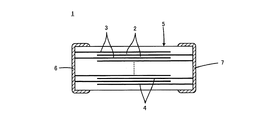
図1は、この発明に係る誘電体セラミックが適用される積層セラミックコンデンサ1を示す断面図である。
FIG. 1 is a cross-sectional view showing a multilayer
積層セラミックコンデンサ1は、積層された複数の誘電体セラミック層2と誘電体セラミック層2間の特定の界面に沿って形成される複数の内部電極3および4とをもって構成される、コンデンサ本体5を備えている。内部電極3および4は、たとえば、Niを主成分としている。
A multilayer
コンデンサ本体5の外表面上の互いに異なる位置には、第1および第2の外部電極6および7が形成される。外部電極6および7は、たとえば、Cuを主成分としている。図1に示した積層セラミックコンデンサ1では、第1および第2の外部電極6および7は、コンデンサ本体5の互いに対向する各端面上に形成される。内部電極3および4は、第1の外部電極6に電気的に接続される複数の第1の内部電極3と第2の外部電極7に電気的に接続される複数の第2の内部電極4とがあり、これら第1および第2の内部電極3および4は、積層方向に関して交互に配置されている。
First and second external electrodes 6 and 7 are formed at different positions on the outer surface of the capacitor body 5. The external electrodes 6 and 7 are mainly composed of Cu, for example. In the monolithic
このような積層セラミックコンデンサ1において、隣り合う第1の内部電極3と第2の内部電極4との間に位置する誘電体セラミック層2の厚みは、1μm未満とされる。
In such a multilayer
誘電体セラミック層2を構成する誘電体セラミックは、主成分がBaTiO3系であり、副成分としてLiを含み、Li含有量e[モル部]が、主成分100モル部に対し、0.5≦e≦6.0である。また、この誘電体セラミックのグレインについて、グレイン径の平均値Rg[μm]が0.06<Rg<0.17であり、その標準偏差σg[μm]がσg<0.075である。
The dielectric ceramic constituting the dielectric
このように、誘電体セラミック層2を構成する誘電体セラミックが、Liを含むとともに、グレイン径が十分に小さく、かつ、粗大粒もないため、誘電体セラミック層2の厚みが1μm未満というに薄層化が進められても、積層セラミックコンデンサ1において、良好な寿命特性を得ることができる。
As described above, the dielectric ceramic constituting the dielectric
寿命特性をより向上させるため、誘電体セラミックは、組成式:100(Ba1-xCax)mTiO3+aRO3/2+bMgO+cMO+dSiO2+eLiO1/2 (m、a、b、c、dおよびeはモル比を示す。RはLa、Ce、Pr、Nd、Sm、Eu、Gd、Tb、Dy、Ho、Er、Tm、Yb、LuおよびYから選ばれる少なくとも1種を含有する。Mは、MnおよびVの少なくとも一方を含有する。)で表されるものとされ、かつ、
0.96≦m≦1.03、
0≦x≦0.2、
0.2≦a≦5.0、
0≦b≦2.0、
0.2≦c≦1.0、および
0.5≦d≦4.0
の各条件を満足するようにされることが好ましい。
In order to further improve the life characteristics, the dielectric ceramic has a composition formula: 100 (Ba 1−x Ca x ) m TiO 3 + aRO 3/2 + bMgO + cMO + dSiO 2 + eLiO 1/2 (m, a, b, c, d and e Represents a molar ratio, R contains at least one selected from La, Ce, Pr, Nd, Sm, Eu, Gd, Tb, Dy, Ho, Er, Tm, Yb, Lu and Y. M is And at least one of Mn and V.), and
0.96 ≦ m ≦ 1.03,
0 ≦ x ≦ 0.2,
0.2 ≦ a ≦ 5.0,
0 ≦ b ≦ 2.0,
0.2 ≦ c ≦ 1.0, and 0.5 ≦ d ≦ 4.0
It is preferable to satisfy the following conditions.
また、寿命特性をより向上させるため、グレイン径の平均値Rg[μm]が0.06<Rg<0.14であり、その標準偏差σg[μm]がσg<0.075であるというように、より限定されることが好ましい。 Further, in order to further improve the life characteristics, the average value Rg [μm] of the grain diameter is 0.06 <Rg <0.14, and the standard deviation σg [μm] is σg <0.075. It is preferable to be more limited.
積層セラミックコンデンサ1を製造するにあたって、コンデンサ本体5の生の状態のものが用意され、これを焼成することが行なわれる。生のコンデンサ本体5は、内部電極3または4となる導電性ペースト膜が形成されたセラミックグリーンシートを含む複数のセラミックグリーンシートが積層されることによって得られる。セラミックグリーンシートは、焼成されたとき、コンデンサ本体5に備える誘電体セラミック層2となる。
When the multilayer
上述したセラミックグリーンシートを作製するため、まず、BaTiO3系を主成分とするBaTiO3系セラミック粉末が用意される。このBaTiO3系セラミック粉末は、その粒径の平均値Rb[μm]が0.06<Rb<0.17であり、その標準偏差σb[μm]がσb<0.065であるようにされる。 To form a ceramic green sheet as described above, first, BaTiO 3 based ceramic powder mainly composed of BaTiO 3 system is prepared. The average particle size Rb [μm] of the BaTiO 3 based ceramic powder is 0.06 <Rb <0.17, and the standard deviation σb [μm] is σb <0.065. .
他方、Li化合物を含む副成分が用意される。 On the other hand, an auxiliary component containing a Li compound is prepared.
そして、上記BaTiO3系セラミック粉末に上記副成分が混合される。これによって、セラミック原料粉末が得られる。このセラミック原料粉末において、Li含有量e[モル部]が、主成分100モル部に対し、0.5≦e≦6.0であるようにされる。 Then, the sub-components are mixed in the BaTiO 3 based ceramic powder. Thereby, a ceramic raw material powder is obtained. In this ceramic raw material powder, the Li content e [mol part] is set to 0.5 ≦ e ≦ 6.0 with respect to 100 mol part of the main component.
次に、セラミック原料粉末にバインダおよび有機溶剤を加えて混合することによって、セラミックスラリーを作製し、このセラミックスラリーをシート状に成形することによって、セラミックグリーンシートを得ることができる。 Next, a ceramic green sheet can be obtained by preparing a ceramic slurry by adding a binder and an organic solvent to the ceramic raw material powder and mixing them, and forming the ceramic slurry into a sheet.
上述のように、セラミックグリーンシートに含まれる、粒度分布がシャープなBaTiO3系セラミック粉末に、適切な量のLiを加えることによって、コンデンサ本体5を得るための焼成工程において、粒成長が適切に抑えられ、シャープな粒度分布をもつグレイン(焼結体の粒子)が得られる。したがって、前述したように、誘電体セラミック層2の厚みが1μm未満というに薄層化が進められても、積層セラミックコンデンサ1において、良好な寿命特性を得ることができる。
As described above, in the firing step for obtaining the capacitor body 5 by adding an appropriate amount of Li to the BaTiO 3 ceramic powder having a sharp particle size distribution contained in the ceramic green sheet, the grain growth is appropriately performed Grains (sintered particles) that are suppressed and have a sharp particle size distribution are obtained. Therefore, as described above, even if the thickness of the dielectric
なお、この発明が適用される積層セラミックコンデンサは、図1に示すような構造を有するものに限らず、たとえば、複数の内部電極がコンデンサ本体内部において直列容量を形成する構造のもの、あるいは、アレイ状の積層セラミックコンデンサまたは低ESL化された積層セラミックコンデンサのような多端子構造のものであってもよい。 The multilayer ceramic capacitor to which the present invention is applied is not limited to the one having the structure as shown in FIG. 1, for example, one having a structure in which a plurality of internal electrodes form a series capacitance inside the capacitor body, or an array A multi-terminal structure such as a multilayer ceramic capacitor having a low ESL shape or a multilayer ceramic capacitor having a reduced ESL may be used.
以下に、この発明に基づいて実施した実験例について説明する。 Below, the experiment example implemented based on this invention is demonstrated.
[実験例1]
実験例1では、グレインの粒度分布およびLi添加量が、寿命特性に与える影響を調べた。
[Experimental Example 1]
In Experimental Example 1, the effects of grain size distribution and Li addition amount on life characteristics were examined.
(A)誘電体原料配合物の作製
まず、主成分の出発原料として、BaCO3およびTiO2を用いて、表1に示す平均粒子径(Rb)および標準偏差(σb)を有するBa1.007TiO3粉末を準備した。平均粒子径(Rb)および標準偏差(σb)は、FE−SEMにて観察し、300個の粒子から、平均円相当径として解析し、算出した。次に、副成分と混合するに先立って、出発原料のBa1.007TiO3粉末を秤量した後、水を媒体としてボールミルにより湿式混合し、凝集体を解砕した。
(A) Preparation of Dielectric Material Compound First, Ba 1.007 TiO 3 having an average particle diameter (Rb) and standard deviation (σb) shown in Table 1 using BaCO 3 and TiO 2 as starting materials of main components. A powder was prepared. The average particle diameter (Rb) and the standard deviation (σb) were observed by FE-SEM, and analyzed and calculated as an average equivalent circle diameter from 300 particles. Next, prior to mixing with the subcomponents , Ba 1.007 TiO 3 powder as a starting material was weighed and wet-mixed by a ball mill using water as a medium to break up the aggregates.
他方、副成分として、Dy2O3、MgCO3、MnCO3、SiO2およびLi2CO3の各粉末を準備し、これらを、
組成式:100Ba1.007TiO3+1.0DyO3/2+0.7MgO+0.3MnO+1.5SiO2+eLiO1/2
で表され、かつ上記組成式中の係数eが表1に示す「Li添加量e」となるように、上記Ba1.007TiO3粉末と配合し、水を媒体としてボールミルにより混合した。その後、蒸発乾燥により試料1〜18の各々に係る誘電体原料配合物を得た。なお、試料1〜9と試料10〜18とは、平均粒子径(Rb)および標準偏差(σb)ならびにLi添加量eの各々については互いに同じであるが、以下に進める積層セラミックコンデンサの作製工程において、セラミック層の厚みが異ならされた点で異なっている。
On the other hand, as an auxiliary component, to prepare each powder of Dy 2 O 3, MgCO 3,
Composition formula: 100Ba 1.007 TiO 3 +1.0 DyO 3/2 + 0.7MgO + 0.3MnO + 1.5SiO 2 + eLiO 1/2
And the Ba 1.007 TiO 3 powder was mixed so that the coefficient e in the composition formula was “Li addition amount e” shown in Table 1, and mixed by a ball mill using water as a medium. Thereafter, a dielectric material composition according to each of
(B)積層セラミックコンデンサの作製
上記誘電体原料配合物に、ポリビニルブチラール系バインダおよびエタノールを加えて、ボールミルにより湿式混合し、セラミックスラリーを得た。このセラミックスラリーをリップコータによりシート成形し、セラミックグリーンシートを得た。このとき、後述するように、セラミックグリーンシートとして、焼成後の厚みが0.9μmとなるものと1.0μmとなるものとの2種類の厚みのものを作製した。
(B) Production of Multilayer Ceramic Capacitor A polyvinyl butyral binder and ethanol were added to the above dielectric material composition, and wet mixed by a ball mill to obtain a ceramic slurry. This ceramic slurry was formed into a sheet by a lip coater to obtain a ceramic green sheet. At this time, as described later, ceramic green sheets having two types of thicknesses were prepared, one having a thickness after firing of 0.9 μm and one having 1.0 μm.
次に、上記セラミックグリーンシート上に、Niを主成分とする導電ペーストをスクリーン印刷し、内部電極を構成するための導電ペースト膜を形成した。 Next, a conductive paste mainly composed of Ni was screen-printed on the ceramic green sheet to form a conductive paste film for constituting an internal electrode.
次に、導電ペースト膜が形成されたセラミックグリーンシートを、導電ペースト膜の引き出されている側が互い違いになるように複数枚積層し、生のコンデンサ本体を得た。次に、この生のコンデンサ本体を、N2雰囲気中にて300℃の温度に加熱し、バインダを燃焼させた後、酸素分圧10-10MPaのH2−N2−H2Oガスからなる還元性雰囲気中にて1025℃の温度で2時間焼成し、焼結したコンデンサ本体を得た。 Next, a plurality of ceramic green sheets on which the conductive paste film was formed were laminated so that the side from which the conductive paste film was drawn was staggered to obtain a raw capacitor body. Next, this raw capacitor body is heated to a temperature of 300 ° C. in an N 2 atmosphere to burn the binder, and then from an H 2 —N 2 —H 2 O gas having an oxygen partial pressure of 10 −10 MPa. The sintered capacitor body was obtained by firing for 2 hours at a temperature of 1025 ° C. in a reducing atmosphere.
次に、上記コンデンサ本体の両端面に、B2O3−Li2O−SiO2−BaOガラスフリットを含有するCuペーストを塗布し、N2雰囲気中において800℃の温度で焼き付け、内部電極と電気的に接続された外部電極を形成し、各試料に係る積層セラミックコンデンサを得た。 Next, a Cu paste containing B 2 O 3 —Li 2 O—SiO 2 —BaO glass frit is applied to both end faces of the capacitor body, and baked at a temperature of 800 ° C. in an N 2 atmosphere. An electrically connected external electrode was formed to obtain a multilayer ceramic capacitor according to each sample.
このようにして得られた積層セラミックコンデンサの外形寸法は、長さ2.0mm、幅1.2mm、厚さ1.0mmであり、内部電極間に介在する誘電体セラミック層の厚みは、表2の「セラミック層厚み」の欄に示すとおりであった。また、有効誘電体セラミック層の数は100であり、1層当たりの対向電極面積は1.4mm2であった。 The outer dimensions of the multilayer ceramic capacitor thus obtained are 2.0 mm in length, 1.2 mm in width, and 1.0 mm in thickness. The thickness of the dielectric ceramic layer interposed between the internal electrodes is as shown in Table 2. In the “Ceramic layer thickness” column. The number of effective dielectric ceramic layers was 100, and the counter electrode area per layer was 1.4 mm 2 .
(C)特性評価およびセラミック微構造観察
特性評価として、誘電率、誘電損失(DF)、容量温度特性、および高温負荷寿命特性を評価した。
(C) Characteristic evaluation and ceramic microstructure observation As characteristic evaluation, dielectric constant, dielectric loss (DF), capacity temperature characteristic, and high temperature load life characteristic were evaluated.
誘電率を求めるための静電容量および誘電損失(DF)は、温度25℃、1kHz、およびAC電圧0.5Vrmsの条件下で測定した。 The capacitance and dielectric loss (DF) for determining the dielectric constant were measured under conditions of a temperature of 25 ° C., 1 kHz, and an AC voltage of 0.5 Vrms.
容量温度特性は、温度変化に対する静電容量の変化率を求めたもので、25℃での静電容量を基準とした−55℃〜85℃の範囲での変化率の最大の値を採用した。−55℃〜85℃の範囲での変化率が±15%以内であれば、EIA規格のX5R特性を満足することになる。 The capacitance-temperature characteristic was obtained by calculating the rate of change of capacitance with respect to temperature change, and the maximum value of the rate of change in the range of −55 ° C. to 85 ° C. based on the capacitance at 25 ° C. was adopted. . If the rate of change in the range of −55 ° C. to 85 ° C. is within ± 15%, the X5R characteristic of the EIA standard is satisfied.
高温負荷寿命特性を求めるため、温度150℃にて、12.5Vの直流電圧を印加して、絶縁抵抗の経時変化を測定する、加速信頼性試験を実施した。この加速信頼性試験において、絶縁抵抗値が105Ω以下になった時点を故障と判定し、この故障に至るまでの時間の平均値、すなわち平均故障時間を求めた。 In order to obtain the high temperature load life characteristics, an accelerated reliability test was performed in which a DC voltage of 12.5 V was applied at a temperature of 150 ° C., and the change over time in the insulation resistance was measured. In this accelerated reliability test, a point in time when the insulation resistance value became 10 5 Ω or less was determined as a failure, and an average value until the failure, that is, an average failure time was obtained.
また、セラミック微構造を観察した。すなわち、試料となる積層セラミックコンデンサの破断面をFE−SEMにて観察し、300個のグレインから、平均円相当径として解析し、平均グレイン径Rgおよびその標準偏差σgを算出した。 Moreover, the ceramic microstructure was observed. That is, the fracture surface of the multilayer ceramic capacitor as a sample was observed with an FE-SEM, analyzed from 300 grains as an average equivalent circle diameter, and an average grain diameter Rg and its standard deviation σg were calculated.
以上の特性評価およびセラミック微構造観察の結果が表2に示されている。 The results of the above characteristic evaluation and ceramic microstructure observation are shown in Table 2.
まず、表2に示した試料のすべてについて、比誘電率が1500以上であり、DFが5%未満であり、温度特性がX5R特性を満たしていた。 First, for all the samples shown in Table 2, the relative dielectric constant was 1500 or more, the DF was less than 5%, and the temperature characteristics satisfied the X5R characteristics.
セラミック層厚みが0.9μmの試料1〜9のうち、Li添加量e[モル部]が0.5≦e≦6.0であるという条件と、平均グレイン径Rg[μm]が0.06<Rg<0.17であるという条件と、その標準偏差σg[μm]がσg<0.075であるという条件との3つの条件をすべて満たす試料1において、良好な寿命特性が得られた。このことから、上記Rg、σgおよびeの3要素の相乗効果により、セラミック層の厚みが1μm未満といった薄層品においても、良好な寿命特性が得られることが明らかとなった。
Among
これは、次のように推測される。副成分中にLiが0.5≦e≦6.0の範囲内で存在することにより、Liが、インヒビターとしてグレイン成長を抑制し、グレイン径分布を狭くするように作用する。グレイン径分布が狭くなることにより、信頼性が改善する。さらに、副成分中にLiが0.5≦e≦6.0の範囲内で存在するときに、平均粒子径Rb[μm]が0.06<Rb<0.17であって、標準偏差σb[μm]がσb<0.065である、チタン酸バリウム系セラミック粉末を主成分として含むセラミック原料粉末を用いると、焼結後の誘電体セラミック中のグレインの粒度分布が大幅に狭くなり、セラミック層の厚みが1.0μm未満の薄層であっても、加速信頼性試験における平均故障時間が100時間以上と信頼性を向上させることができる。 This is presumed as follows. When Li is present in the subcomponent within the range of 0.5 ≦ e ≦ 6.0, Li acts as an inhibitor to suppress grain growth and narrow the grain diameter distribution. Narrow grain size distribution improves reliability. Further, when Li is present in the subcomponent within the range of 0.5 ≦ e ≦ 6.0, the average particle diameter Rb [μm] is 0.06 <Rb <0.17, and the standard deviation σb When ceramic raw material powder containing [μm] σb <0.065 as a main component and containing barium titanate ceramic powder as a main component, the grain size distribution in the sintered dielectric ceramic is significantly narrowed. Even if the thickness of the layer is less than 1.0 μm, the reliability can be improved with an average failure time of 100 hours or more in the accelerated reliability test.
なお、セラミック層の厚みが1.0μmの試料10〜18においても、試料1のように、Li添加量e[モル部]が0.5≦e≦6.0であるという条件と、平均グレイン径Rg[μm]が0.06<Rg<0.17であるという条件と、その標準偏差σg[μm]がσg<0.075であるという条件との3つの条件をすべて満たせば、試料10のように、良好な寿命特性が得られた。しかしながら、寿命特性について、セラミック層の厚みが1μm以上の試料間で比較する場合に比べて、セラミック層の厚みが1.0μm未満の試料間で比較する場合の方が、上記3つの条件を満たす試料とそうでない試料との差がより顕著であった。
In Samples 10 to 18 having a ceramic layer thickness of 1.0 μm, as in
[実験例2]
実験例2は、寿命特性向上にとって、より好ましい組成範囲を規定するために実施したものである。
[Experiment 2]
Experimental Example 2 was carried out in order to define a more preferable composition range for improving the life characteristics.
(A)誘電体原料配合物の作製
まず、主成分の出発原料として、BaCO3、CaCO3およびTiO2の各粉末を準備し、これら粉末を、表3に示されたmおよびxをそれぞれ有する(Ba1-xCax)mTiO3の組成になるように秤量し、次いで、熱処理し、表3に示す平均粒子径(Rb)および標準偏差(σb)を有する(Ba1-xCax)mTiO3粉末を得た。次に、副成分と混合するに先立って、出発原料の(Ba1-xCax)mTiO3粉末を秤量した後、水を媒体としてボールミルにより湿式混合し、凝集体を解砕した。
(A) Preparation of dielectric raw material blend First, BaCO 3 , CaCO 3, and TiO 2 powders are prepared as starting materials for the main components, and these powders have m and x shown in Table 3, respectively. Weighed to a composition of (Ba 1-x Ca x ) m TiO 3 , then heat-treated, and had the average particle diameter (Rb) and standard deviation (σb) shown in Table 3 (Ba 1-x Ca x ) was obtained m TiO 3 powder. Next, prior to mixing with the subcomponents, the starting material (Ba 1-x Ca x ) m TiO 3 powder was weighed and wet-mixed with a ball mill using water as a medium to break up the aggregates.
他方、副成分として、R(Rは、La、Ce、Pr、Nd、Sm、Eu、Gd、Tb、Dy、Ho、Er、Tm、Yb、LuおよびYから選ばれる1種である。)、Mg、M(Mは、MnおよびVの少なくとも一方である。)、SiおよびLiの各々の酸化物または炭酸塩の各粉末を準備し、これらを、
組成式:100(Ba1-xCax)mTiO3+aRO3/2+bMgO+cMO+dSiO2+eLiO1/2
で表され、かつ表3にそれぞれ示す、M成分およびR成分をそれぞれ用いながら、係数a、b、c、dおよびeを有する組成となるように、上記(Ba1-xCax)mTiO3粉末と配合し、水を媒体としてボールミルにより混合した。その後、蒸発乾燥により試料101〜128の各々に係る誘電体原料配合物を得た。
On the other hand, R (R is one selected from La, Ce, Pr, Nd, Sm, Eu, Gd, Tb, Dy, Ho, Er, Tm, Yb, Lu, and Y as a subcomponent). Mg, M (M is at least one of Mn and V), each powder of each oxide or carbonate of Si and Li are prepared,
Composition formula: 100 (Ba 1-x Ca x ) m TiO 3 + aRO 3/2 + bMgO + cMO + dSiO 2 + eLiO 1/2
(Ba 1-x Ca x ) m TiO so as to have a composition having coefficients a, b, c, d, and e, using the M component and the R component shown in Table 3, respectively. 3 powders were mixed and mixed by a ball mill using water as a medium. Then, the dielectric raw material formulation which concerns on each of the samples 101-128 was obtained by evaporation drying.
(B)積層セラミックコンデンサの作製
実験例1の場合と同様の操作を経て、各試料に係る積層セラミックコンデンサを得た。誘電体セラミック層の厚みは、0.8μmとした。
(B) Production of Multilayer Ceramic Capacitor The same operation as in Experimental Example 1 was performed to obtain a multilayer ceramic capacitor according to each sample. The thickness of the dielectric ceramic layer was 0.8 μm.
(C)特性評価およびセラミック微構造観察
実験例1の場合と同様の特性評価およびセラミック微構造観察を行なった。その結果が表4に示されている。
(C) Characteristic evaluation and ceramic microstructure observation Characteristic evaluation and ceramic microstructure observation similar to those in Experimental Example 1 were performed. The results are shown in Table 4.
まず、表4に示した試料のすべてについて、この発明の範囲内にあり、DFが5%未満であり、110時間以上の平均故障時間を示した。 First, all of the samples shown in Table 4 were within the scope of the present invention, DF was less than 5%, and showed an average failure time of 110 hours or more.
しかしながら、表4に示した試料のうち、特に試料101〜118については、
組成式:100(Ba1-xCax)mTiO3+aRO3/2+bMgO+cMO+dSiO2+eLiO1/2において、
0.96≦m≦1.03、
0≦x≦0.2、
0.2≦a≦5.0、
0≦b≦2.0、
0.2≦c≦1.0、および
0.5≦d≦4.0
の各条件を満足しており、その結果、比誘電率が1500以上であり、温度特性がX5R特性を満足し、平均故障時間が150時間以上であって寿命特性がより向上している。
However, among the samples shown in Table 4, especially for the samples 101 to 118,
Composition formula: 100 (Ba 1−x Ca x ) m TiO 3 + aRO 3/2 + bMgO + cMO + dSiO 2 + eLiO 1/2
0.96 ≦ m ≦ 1.03,
0 ≦ x ≦ 0.2,
0.2 ≦ a ≦ 5.0,
0 ≦ b ≦ 2.0,
0.2 ≦ c ≦ 1.0, and 0.5 ≦ d ≦ 4.0
As a result, the relative dielectric constant is 1500 or more, the temperature characteristics satisfy the X5R characteristics, the average failure time is 150 hours or more, and the life characteristics are further improved.
これらに対して、mに関して、m<0.960である試料119では、平均故障時間が150時間未満と短く、他方、m>1.030である試料120では、比誘電率が1500未満と低く、平均故障時間が150時間未満と短い。 On the other hand, with respect to m, in sample 119 where m <0.960, the average failure time is as short as less than 150 hours, while in sample 120 where m> 1.030, the relative dielectric constant is as low as less than 1500. The average failure time is as short as less than 150 hours.
また、xに関して、x>0.20である試料121では、平均故障時間が150時間未満と短い。 Further, with respect to x, in the sample 121 where x> 0.20, the average failure time is as short as less than 150 hours.
また、aに関して、a<0.2である試料122では、平均故障時間が150時間未満と短く、他方、a>5.0である試料123では、誘電率の温度変化率の絶対値が15%以上と大きく、平均故障時間が150時間未満と短い。 Regarding a, in Sample 122 where a <0.2, the average failure time is as short as less than 150 hours, while in Sample 123 where a> 5.0, the absolute value of the temperature change rate of the dielectric constant is 15 %, And the average failure time is as short as less than 150 hours.
また、bに関して、b>2.0である試料124では、平均故障時間が150時間未満と短い。 Regarding b, in the sample 124 where b> 2.0, the average failure time is as short as less than 150 hours.
また、cに関して、c<0.2である試料125では、平均故障時間が150時間未満と短く、他方、c>1.0である試料126でも、平均故障時間が150時間未満と短い。 Regarding c, in sample 125 where c <0.2, the average failure time is as short as less than 150 hours, while in sample 126 where c> 1.0, the average failure time is as short as less than 150 hours.
また、dに関して、d<0.5である試料127では、平均故障時間が150時間未満と短く、他方、d>4.0である試料128では、誘電率の温度変化率の絶対値が15%以上と大きく、平均故障時間が150時間未満と短い。 Further, with respect to d, in sample 127 where d <0.5, the average failure time is as short as less than 150 hours, while in sample 128 where d> 4.0, the absolute value of the temperature change rate of the dielectric constant is 15 %, And the average failure time is as short as less than 150 hours.
[実験例3]
実験例3は、平均グレイン径について、より好ましい範囲を求めようとするものである。
[Experiment 3]
Experimental Example 3 seeks a more preferable range for the average grain diameter.
(A)誘電体原料配合物の作製
表5に示す平均粒子径(Rb)および標準偏差(σb)を有するBaTiO3系粉末を用いたことを除いて、実験例1における試料1に係る誘電体原料配合物の場合と同様にして、試料201および202の各々に係る誘電体原料配合物を得た。
(A) Preparation of dielectric raw material blend Dielectric according to
(B)積層セラミックコンデンサの作製
実験例1の場合と同様の操作を経て、各試料に係る積層セラミックコンデンサを得た。誘電体セラミック層の厚みは、0.9μmとした。
(B) Production of Multilayer Ceramic Capacitor The same operation as in Experimental Example 1 was performed to obtain a multilayer ceramic capacitor according to each sample. The thickness of the dielectric ceramic layer was 0.9 μm.
(C)特性評価およびセラミック微構造観察
実験例1の場合と同様の特性評価およびセラミック微構造観察を行なった。特性評価の結果が表6に示されている。
(C) Characteristic evaluation and ceramic microstructure observation Characteristic evaluation and ceramic microstructure observation similar to those in Experimental Example 1 were performed. The results of characterization are shown in Table 6.
表6に示すように、平均グレイン径Rg[μm]が0.06<Rg<0.14の範囲内にある試料201の方が、この範囲から外れる試料202に比べて、寿命特性がさらに良好である。 As shown in Table 6, the sample 201 in which the average grain diameter Rg [μm] is in the range of 0.06 <Rg <0.14 has better life characteristics than the sample 202 that is out of this range. It is.
1 積層セラミックコンデンサ
2 誘電体セラミック層
3,4 内部電極
5 コンデンサ本体
6,7 外部電極
1
Claims (5)
副成分としてLiを含み、Li含有量e[モル部]が、主成分100モル部に対し、0.5≦e≦6.0であり、
当該誘電体セラミックのグレインについて、グレイン径の平均値Rg[μm]が0.06<Rg<0.17であり、その標準偏差σg[μm]がσg<0.075である、
誘電体セラミック。 A dielectric ceramic whose main component is a BaTiO 3 system,
Li is contained as a subcomponent, and the Li content e [mol part] is 0.5 ≦ e ≦ 6.0 with respect to 100 mol part of the main component,
For the grains of the dielectric ceramic, the average grain diameter Rg [μm] is 0.06 <Rg <0.17, and the standard deviation σg [μm] is σg <0.075.
Dielectric ceramic.
0.96≦m≦1.03、
0≦x≦0.2、
0.2≦a≦5.0、
0≦b≦2.0、
0.2≦c≦1.0、および
0.5≦d≦4.0
の各条件を満足する、請求項1に記載の誘電体セラミック。 Composition formula: 100 (Ba 1−x Ca x ) m TiO 3 + aRO 3/2 + bMgO + cMO + dSiO 2 + eLiO 1/2 (m, a, b, c, d, and e represent molar ratios, R represents La, Ce, Pr Nd, Sm, Eu, Gd, Tb, Dy, Ho, Er, Tm, Yb, Lu, and Y. M contains at least one of Mn and V). And
0.96 ≦ m ≦ 1.03,
0 ≦ x ≦ 0.2,
0.2 ≦ a ≦ 5.0,
0 ≦ b ≦ 2.0,
0.2 ≦ c ≦ 1.0, and 0.5 ≦ d ≦ 4.0
The dielectric ceramic according to claim 1, wherein each of the following conditions is satisfied.
前記コンデンサ本体の外表面上の互いに異なる位置に形成され、かつ前記内部電極の特定のものに電気的に接続される、複数の外部電極と
を備え、
前記内部電極の積層方向に隣り合うものの間に位置する前記誘電体セラミック層の厚みは1μm未満であり、かつ、
前記誘電体セラミック層は、請求項1ないし3のいずれかに記載の誘電体セラミックからなる、
積層セラミックコンデンサ。 A capacitor body comprising a plurality of laminated dielectric ceramic layers and a plurality of internal electrodes formed along a specific interface between the dielectric ceramic layers;
A plurality of external electrodes formed at different positions on the outer surface of the capacitor body and electrically connected to a specific one of the internal electrodes;
The thickness of the dielectric ceramic layer located between adjacent ones of the internal electrodes in the stacking direction is less than 1 μm, and
The dielectric ceramic layer is made of the dielectric ceramic according to any one of claims 1 to 3.
Multilayer ceramic capacitor.
Li化合物を含む副成分を用意する工程と、
前記BaTiO3系セラミック粉末に前記副成分を混合することによって、セラミック原料粉末を得る工程と、
前記セラミック原料粉末を成形することによって、セラミック成形体を得る工程と、
前記セラミック成形体を焼成することによって、誘電体セラミックを得る工程と
を備え、
前記セラミック原料粉末において、Li含有量e[モル部]が、主成分100モル部に対し、0.5≦e≦6.0であり、
前記BaTiO3系セラミック粉末において、粒径の平均値Rb[μm]が0.06<Rb<0.17であり、その標準偏差σb[μm]がσb<0.065である、
誘電体セラミックの製造方法。 Preparing a BaTiO 3 ceramic powder mainly composed of BaTiO 3 system,
Preparing a subcomponent containing a Li compound;
A step of obtaining a ceramic raw material powder by mixing the subcomponent with the BaTiO 3 based ceramic powder;
A step of obtaining a ceramic molded body by molding the ceramic raw material powder;
Obtaining a dielectric ceramic by firing the ceramic molded body,
In the ceramic raw material powder, the Li content e [mol part] is 0.5 ≦ e ≦ 6.0 with respect to 100 mol part of the main component,
In the BaTiO 3 based ceramic powder, the average value Rb [μm] of the particle diameter is 0.06 <Rb <0.17, and the standard deviation σb [μm] is σb <0.065.
A method for producing a dielectric ceramic.
Priority Applications (4)
| Application Number | Priority Date | Filing Date | Title |
|---|---|---|---|
| JP2008217585A JP5109872B2 (en) | 2008-08-27 | 2008-08-27 | Multilayer ceramic capacitor and manufacturing method thereof |
| US12/540,743 US8248754B2 (en) | 2008-08-27 | 2009-08-13 | Dielectric ceramic, method for producing dielectric ceramic, and monolithic ceramic capacitor |
| CN2009101666644A CN101665354B (en) | 2008-08-27 | 2009-08-26 | Dielectric ceramic, producing method thereof and monolithic ceramic capacitor |
| KR1020090079608A KR101064475B1 (en) | 2008-08-27 | 2009-08-27 | Dielectric ceramic, method for producing dielectric ceramic, and monolithic ceramic capacitor |
Applications Claiming Priority (1)
| Application Number | Priority Date | Filing Date | Title |
|---|---|---|---|
| JP2008217585A JP5109872B2 (en) | 2008-08-27 | 2008-08-27 | Multilayer ceramic capacitor and manufacturing method thereof |
Publications (2)
| Publication Number | Publication Date |
|---|---|
| JP2010052964A true JP2010052964A (en) | 2010-03-11 |
| JP5109872B2 JP5109872B2 (en) | 2012-12-26 |
Family
ID=41725133
Family Applications (1)
| Application Number | Title | Priority Date | Filing Date |
|---|---|---|---|
| JP2008217585A Active JP5109872B2 (en) | 2008-08-27 | 2008-08-27 | Multilayer ceramic capacitor and manufacturing method thereof |
Country Status (4)
| Country | Link |
|---|---|
| US (1) | US8248754B2 (en) |
| JP (1) | JP5109872B2 (en) |
| KR (1) | KR101064475B1 (en) |
| CN (1) | CN101665354B (en) |
Cited By (6)
| Publication number | Priority date | Publication date | Assignee | Title |
|---|---|---|---|---|
| WO2012120712A1 (en) * | 2011-03-04 | 2012-09-13 | 太陽誘電株式会社 | Laminated ceramic capacitor |
| JP2012214316A (en) * | 2011-03-31 | 2012-11-08 | Tdk Corp | Dielectric ceramic composition and electronic component |
| JP2013112536A (en) * | 2011-11-25 | 2013-06-10 | Samsung Electro-Mechanics Co Ltd | Method for manufacturing high dielectric constant ceramics |
| JP2014022714A (en) * | 2012-07-20 | 2014-02-03 | Samsung Electro-Mechanics Co Ltd | Multilayer ceramic electronic component and method of manufacturing the same |
| JP2016117605A (en) * | 2014-12-19 | 2016-06-30 | サムソン エレクトロ−メカニックス カンパニーリミテッド. | Dielectric ceramic and production method thereof |
| JP7421313B2 (en) | 2019-11-22 | 2024-01-24 | 太陽誘電株式会社 | Ceramic electronic components and their manufacturing method |
Families Citing this family (4)
| Publication number | Priority date | Publication date | Assignee | Title |
|---|---|---|---|---|
| KR102000686B1 (en) * | 2011-10-21 | 2019-07-17 | 삼성전기주식회사 | Laminated ceramic electronic parts |
| JP6655706B2 (en) * | 2015-07-17 | 2020-02-26 | ティーディーケイ・エレクトロニクス・アクチェンゲゼルシャフトTdk Electronics Ag | Dielectric composition, dielectric element, electronic component and laminated electronic component |
| CN107721409A (en) * | 2017-10-09 | 2018-02-23 | 宁夏钜晶电子材料科技有限公司 | Multilayer sheet type thermal sensitive ceramics device preparation method |
| KR20230174839A (en) | 2022-06-22 | 2023-12-29 | 공주대학교 산학협력단 | Artificial layer made of bimodal sized dielectric material and Zn-Mn secondary battery including thereof |
Citations (10)
| Publication number | Priority date | Publication date | Assignee | Title |
|---|---|---|---|---|
| JP2007258661A (en) * | 2005-09-28 | 2007-10-04 | Kyocera Corp | Laminated ceramic capacitor and its manufacturing method |
| WO2008066119A1 (en) * | 2006-11-29 | 2008-06-05 | Kyocera Corporation | Dielectric ceramic and capacitor |
| JP2008133162A (en) * | 2006-11-29 | 2008-06-12 | Kyocera Corp | Barium titanate powder, its producing method and dielectric porcelain |
| JP2008133163A (en) * | 2006-11-29 | 2008-06-12 | Kyocera Corp | Barium titanate powder, its producing method and dielectric porcelain |
| WO2008114619A1 (en) * | 2007-03-16 | 2008-09-25 | Kyocera Corporation | Dielectric ceramic and capacitor |
| WO2009119444A1 (en) * | 2008-03-24 | 2009-10-01 | 京セラ株式会社 | Laminated ceramic capacitor |
| WO2009119613A1 (en) * | 2008-03-25 | 2009-10-01 | 京セラ株式会社 | Multilayer ceramic capacitor |
| WO2009119614A1 (en) * | 2008-03-24 | 2009-10-01 | 京セラ株式会社 | Multilayer ceramic capacitor |
| JP2010006634A (en) * | 2008-06-26 | 2010-01-14 | Kyocera Corp | Dielectric ceramic and laminated ceramic capacitor using the same |
| JP2010006633A (en) * | 2008-06-26 | 2010-01-14 | Kyocera Corp | Dielectric ceramic and multilayered ceramic capacitor using the same |
Family Cites Families (16)
| Publication number | Priority date | Publication date | Assignee | Title |
|---|---|---|---|---|
| US171938A (en) | 1876-01-11 | Improvement in tinners fire-pots | ||
| JPH0750753B2 (en) | 1987-08-21 | 1995-05-31 | 株式会社東芝 | Transistor device |
| JP3024537B2 (en) * | 1995-12-20 | 2000-03-21 | 株式会社村田製作所 | Multilayer ceramic capacitors |
| JP3487539B2 (en) * | 1997-05-06 | 2004-01-19 | 太陽誘電株式会社 | Dielectric porcelain |
| JP3878778B2 (en) | 1999-07-21 | 2007-02-07 | Tdk株式会社 | Dielectric porcelain composition and electronic component |
| KR100428962B1 (en) | 1999-10-05 | 2004-04-29 | 티디케이가부시기가이샤 | Process for producing dielectric ceramic composition |
| JP4407299B2 (en) | 2004-01-30 | 2010-02-03 | Tdk株式会社 | Multilayer ceramic capacitor |
| JP4483659B2 (en) * | 2005-04-04 | 2010-06-16 | Tdk株式会社 | Electronic component, dielectric ceramic composition and method for producing the same |
| JP4936825B2 (en) * | 2006-08-02 | 2012-05-23 | 太陽誘電株式会社 | Multilayer ceramic capacitor |
| JP2008066119A (en) | 2006-09-07 | 2008-03-21 | Ricoh Co Ltd | Power supply controller, interlock apparatus, and electrical equipment |
| JP2008114619A (en) | 2006-10-31 | 2008-05-22 | Mitsubishi Fuso Truck & Bus Corp | Panel mounting structure of vehicle |
| JP5071070B2 (en) | 2007-09-18 | 2012-11-14 | Nok株式会社 | Hollow fiber membrane module and method for producing hollow fiber membrane module |
| JP5119871B2 (en) | 2007-11-12 | 2013-01-16 | セイコーエプソン株式会社 | Printer |
| JP2009119613A (en) | 2007-11-12 | 2009-06-04 | Toray Ind Inc | Fiber-reinforced plastic molding and its production method |
| EP2320936A1 (en) | 2008-07-16 | 2011-05-18 | PAION Deutschland GmbH | Prevention and treatment of radiation injury |
| WO2010006633A1 (en) | 2008-07-18 | 2010-01-21 | Siemens Aktiengesellschaft | Method for operating an automation system, computer program, and computer program product |
-
2008
- 2008-08-27 JP JP2008217585A patent/JP5109872B2/en active Active
-
2009
- 2009-08-13 US US12/540,743 patent/US8248754B2/en active Active
- 2009-08-26 CN CN2009101666644A patent/CN101665354B/en active Active
- 2009-08-27 KR KR1020090079608A patent/KR101064475B1/en active IP Right Grant
Patent Citations (10)
| Publication number | Priority date | Publication date | Assignee | Title |
|---|---|---|---|---|
| JP2007258661A (en) * | 2005-09-28 | 2007-10-04 | Kyocera Corp | Laminated ceramic capacitor and its manufacturing method |
| WO2008066119A1 (en) * | 2006-11-29 | 2008-06-05 | Kyocera Corporation | Dielectric ceramic and capacitor |
| JP2008133162A (en) * | 2006-11-29 | 2008-06-12 | Kyocera Corp | Barium titanate powder, its producing method and dielectric porcelain |
| JP2008133163A (en) * | 2006-11-29 | 2008-06-12 | Kyocera Corp | Barium titanate powder, its producing method and dielectric porcelain |
| WO2008114619A1 (en) * | 2007-03-16 | 2008-09-25 | Kyocera Corporation | Dielectric ceramic and capacitor |
| WO2009119444A1 (en) * | 2008-03-24 | 2009-10-01 | 京セラ株式会社 | Laminated ceramic capacitor |
| WO2009119614A1 (en) * | 2008-03-24 | 2009-10-01 | 京セラ株式会社 | Multilayer ceramic capacitor |
| WO2009119613A1 (en) * | 2008-03-25 | 2009-10-01 | 京セラ株式会社 | Multilayer ceramic capacitor |
| JP2010006634A (en) * | 2008-06-26 | 2010-01-14 | Kyocera Corp | Dielectric ceramic and laminated ceramic capacitor using the same |
| JP2010006633A (en) * | 2008-06-26 | 2010-01-14 | Kyocera Corp | Dielectric ceramic and multilayered ceramic capacitor using the same |
Cited By (7)
| Publication number | Priority date | Publication date | Assignee | Title |
|---|---|---|---|---|
| WO2012120712A1 (en) * | 2011-03-04 | 2012-09-13 | 太陽誘電株式会社 | Laminated ceramic capacitor |
| US8908353B2 (en) | 2011-03-04 | 2014-12-09 | Taiyo Yuden Co., Ltd. | Laminated ceramic capacitor |
| JP2012214316A (en) * | 2011-03-31 | 2012-11-08 | Tdk Corp | Dielectric ceramic composition and electronic component |
| JP2013112536A (en) * | 2011-11-25 | 2013-06-10 | Samsung Electro-Mechanics Co Ltd | Method for manufacturing high dielectric constant ceramics |
| JP2014022714A (en) * | 2012-07-20 | 2014-02-03 | Samsung Electro-Mechanics Co Ltd | Multilayer ceramic electronic component and method of manufacturing the same |
| JP2016117605A (en) * | 2014-12-19 | 2016-06-30 | サムソン エレクトロ−メカニックス カンパニーリミテッド. | Dielectric ceramic and production method thereof |
| JP7421313B2 (en) | 2019-11-22 | 2024-01-24 | 太陽誘電株式会社 | Ceramic electronic components and their manufacturing method |
Also Published As
| Publication number | Publication date |
|---|---|
| KR101064475B1 (en) | 2011-09-15 |
| JP5109872B2 (en) | 2012-12-26 |
| KR20100025493A (en) | 2010-03-09 |
| CN101665354A (en) | 2010-03-10 |
| US8248754B2 (en) | 2012-08-21 |
| CN101665354B (en) | 2013-04-03 |
| US20100053843A1 (en) | 2010-03-04 |
Similar Documents
| Publication | Publication Date | Title |
|---|---|---|
| JP5109872B2 (en) | Multilayer ceramic capacitor and manufacturing method thereof | |
| JP5811103B2 (en) | Multilayer ceramic capacitor and method for manufacturing multilayer ceramic capacitor | |
| JP4992918B2 (en) | Dielectric ceramic and multilayer ceramic capacitors | |
| JP5224147B2 (en) | Dielectric ceramic and multilayer ceramic capacitor | |
| JP5565528B2 (en) | Multilayer ceramic capacitor and method of manufacturing multilayer ceramic capacitor | |
| JP4831142B2 (en) | Dielectric ceramic and multilayer ceramic capacitors | |
| JP5316353B2 (en) | Dielectric ceramic and multilayer ceramic capacitors | |
| JP5152017B2 (en) | Dielectric ceramic and multilayer ceramic capacitors | |
| JPWO2015040869A1 (en) | Multilayer ceramic capacitor and manufacturing method thereof | |
| JP5370212B2 (en) | Dielectric ceramic and multilayer ceramic capacitors | |
| JP5409443B2 (en) | Multilayer ceramic capacitor | |
| JP4697582B2 (en) | Dielectric ceramic, dielectric ceramic manufacturing method, and multilayer ceramic capacitor | |
| CN104003711B (en) | Dielectric ceramic composition and electronic unit | |
| JP4548423B2 (en) | Dielectric ceramic and multilayer ceramic capacitors | |
| JP5655866B2 (en) | Multilayer ceramic capacitor and method for manufacturing multilayer ceramic capacitor | |
| JP2010208905A (en) | Method for manufacturing dielectric ceramic, dielectric ceramic, method for manufacturing laminated ceramic capacitor and the laminated ceramic capacitor | |
| JP2011071162A (en) | Multilayer ceramic electronic component | |
| JP2014112730A (en) | Laminated ceramic capacitor | |
| JP2011162401A (en) | Dielectric ceramic and laminated ceramic capacitor | |
| JP2013065592A (en) | Laminated ceramic capacitor | |
| JP2005263508A (en) | Dielectric ceramic composition, laminated porcelain capacitor, and method for producing the capacitor | |
| JP5729419B2 (en) | Multilayer ceramic capacitor | |
| JP5354834B2 (en) | Dielectric porcelain composition, porcelain capacitor and method for producing the same | |
| JP5516763B2 (en) | Dielectric ceramic and multilayer ceramic capacitors | |
| JP2005272263A (en) | Dielectric ceramic composition, multilayer ceramic capacitor and its manufacturing method |
Legal Events
| Date | Code | Title | Description |
|---|---|---|---|
| A621 | Written request for application examination |
Free format text: JAPANESE INTERMEDIATE CODE: A621 Effective date: 20101117 |
|
| A977 | Report on retrieval |
Free format text: JAPANESE INTERMEDIATE CODE: A971007 Effective date: 20120130 |
|
| A131 | Notification of reasons for refusal |
Free format text: JAPANESE INTERMEDIATE CODE: A131 Effective date: 20120214 |
|
| A521 | Request for written amendment filed |
Free format text: JAPANESE INTERMEDIATE CODE: A523 Effective date: 20120309 |
|
| TRDD | Decision of grant or rejection written | ||
| A01 | Written decision to grant a patent or to grant a registration (utility model) |
Free format text: JAPANESE INTERMEDIATE CODE: A01 Effective date: 20120911 |
|
| A01 | Written decision to grant a patent or to grant a registration (utility model) |
Free format text: JAPANESE INTERMEDIATE CODE: A01 |
|
| A61 | First payment of annual fees (during grant procedure) |
Free format text: JAPANESE INTERMEDIATE CODE: A61 Effective date: 20120924 |
|
| FPAY | Renewal fee payment (event date is renewal date of database) |
Free format text: PAYMENT UNTIL: 20151019 Year of fee payment: 3 |
|
| R150 | Certificate of patent or registration of utility model |
Ref document number: 5109872 Country of ref document: JP Free format text: JAPANESE INTERMEDIATE CODE: R150 Free format text: JAPANESE INTERMEDIATE CODE: R150 |