JP2010045034A - Organic light emitting element equipped with optical efficiency improving layer - Google Patents
Organic light emitting element equipped with optical efficiency improving layer Download PDFInfo
- Publication number
- JP2010045034A JP2010045034A JP2009189375A JP2009189375A JP2010045034A JP 2010045034 A JP2010045034 A JP 2010045034A JP 2009189375 A JP2009189375 A JP 2009189375A JP 2009189375 A JP2009189375 A JP 2009189375A JP 2010045034 A JP2010045034 A JP 2010045034A
- Authority
- JP
- Japan
- Prior art keywords
- group
- substituted
- unsubstituted
- emitting device
- organic light
- Prior art date
- Legal status (The legal status is an assumption and is not a legal conclusion. Google has not performed a legal analysis and makes no representation as to the accuracy of the status listed.)
- Granted
Links
- 230000003287 optical effect Effects 0.000 title abstract 3
- 150000001875 compounds Chemical class 0.000 claims abstract description 26
- 229910052757 nitrogen Inorganic materials 0.000 claims abstract description 21
- 239000010410 layer Substances 0.000 claims description 141
- 239000012044 organic layer Substances 0.000 claims description 46
- 125000003118 aryl group Chemical group 0.000 claims description 29
- 239000000126 substance Substances 0.000 claims description 19
- 125000001072 heteroaryl group Chemical group 0.000 claims description 17
- 239000000758 substrate Substances 0.000 claims description 15
- 125000004093 cyano group Chemical group *C#N 0.000 claims description 14
- 125000004435 hydrogen atom Chemical class [H]* 0.000 claims description 14
- 125000000732 arylene group Chemical group 0.000 claims description 12
- 125000002252 acyl group Chemical group 0.000 claims description 10
- 125000005843 halogen group Chemical group 0.000 claims description 10
- 125000005549 heteroarylene group Chemical group 0.000 claims description 10
- 125000002887 hydroxy group Chemical group [H]O* 0.000 claims description 10
- 125000001424 substituent group Chemical group 0.000 claims description 9
- 125000000923 (C1-C30) alkyl group Chemical group 0.000 claims description 8
- 125000003545 alkoxy group Chemical group 0.000 claims description 8
- 125000000304 alkynyl group Chemical group 0.000 claims description 8
- 229910052739 hydrogen Inorganic materials 0.000 claims description 8
- 239000001257 hydrogen Substances 0.000 claims description 8
- 125000000008 (C1-C10) alkyl group Chemical group 0.000 claims description 7
- 230000006872 improvement Effects 0.000 claims description 7
- 125000000739 C2-C30 alkenyl group Chemical group 0.000 claims description 6
- 125000001997 phenyl group Chemical group [H]C1=C([H])C([H])=C(*)C([H])=C1[H] 0.000 claims description 6
- 125000004957 naphthylene group Chemical group 0.000 claims description 5
- 125000000843 phenylene group Chemical group C1(=C(C=CC=C1)*)* 0.000 claims description 5
- 125000005566 carbazolylene group Chemical group 0.000 claims description 4
- 125000005567 fluorenylene group Chemical group 0.000 claims description 4
- 125000005559 triazolylene group Chemical group 0.000 claims description 4
- 125000006374 C2-C10 alkenyl group Chemical group 0.000 claims description 3
- 125000005865 C2-C10alkynyl group Chemical group 0.000 claims description 3
- 125000005551 pyridylene group Chemical group 0.000 claims description 3
- 229920006395 saturated elastomer Polymers 0.000 claims description 3
- 125000000027 (C1-C10) alkoxy group Chemical group 0.000 claims description 2
- KAKZBPTYRLMSJV-UHFFFAOYSA-N Butadiene Chemical group C=CC=C KAKZBPTYRLMSJV-UHFFFAOYSA-N 0.000 claims description 2
- 125000004653 anthracenylene group Chemical group 0.000 claims description 2
- 229910052799 carbon Inorganic materials 0.000 claims description 2
- 125000005584 chrysenylene group Chemical group 0.000 claims description 2
- MHAUGLFOVCQYNR-UHFFFAOYSA-N pentaphenylene Chemical group C1=CC=C2C3=CC=CC=C3C3=CC=CC=C3C3=CC=CC=C3C3=CC=CC=C3C2=C1 MHAUGLFOVCQYNR-UHFFFAOYSA-N 0.000 claims description 2
- 125000005550 pyrazinylene group Chemical group 0.000 claims description 2
- 125000005548 pyrenylene group Chemical group 0.000 claims description 2
- 125000005576 pyrimidinylene group Chemical group 0.000 claims description 2
- 125000005730 thiophenylene group Chemical group 0.000 claims description 2
- 238000002347 injection Methods 0.000 description 34
- 239000007924 injection Substances 0.000 description 34
- -1 phthalocyanine compound Chemical class 0.000 description 24
- 230000015572 biosynthetic process Effects 0.000 description 23
- XEKOWRVHYACXOJ-UHFFFAOYSA-N Ethyl acetate Chemical compound CCOC(C)=O XEKOWRVHYACXOJ-UHFFFAOYSA-N 0.000 description 21
- OKKJLVBELUTLKV-UHFFFAOYSA-N Methanol Chemical compound OC OKKJLVBELUTLKV-UHFFFAOYSA-N 0.000 description 21
- 238000006243 chemical reaction Methods 0.000 description 20
- 239000000463 material Substances 0.000 description 20
- 238000000034 method Methods 0.000 description 18
- 230000005525 hole transport Effects 0.000 description 17
- 238000003786 synthesis reaction Methods 0.000 description 17
- WYURNTSHIVDZCO-UHFFFAOYSA-N Tetrahydrofuran Chemical compound C1CCOC1 WYURNTSHIVDZCO-UHFFFAOYSA-N 0.000 description 16
- 238000004528 spin coating Methods 0.000 description 15
- 125000000217 alkyl group Chemical group 0.000 description 12
- 239000000243 solution Substances 0.000 description 11
- 238000001771 vacuum deposition Methods 0.000 description 10
- YMWUJEATGCHHMB-UHFFFAOYSA-N Dichloromethane Chemical compound ClCCl YMWUJEATGCHHMB-UHFFFAOYSA-N 0.000 description 9
- 239000002019 doping agent Substances 0.000 description 9
- HEDRZPFGACZZDS-UHFFFAOYSA-N Chloroform Chemical compound ClC(Cl)Cl HEDRZPFGACZZDS-UHFFFAOYSA-N 0.000 description 8
- 238000000151 deposition Methods 0.000 description 8
- 239000011541 reaction mixture Substances 0.000 description 8
- YLQBMQCUIZJEEH-UHFFFAOYSA-N tetrahydrofuran Natural products C=1C=COC=1 YLQBMQCUIZJEEH-UHFFFAOYSA-N 0.000 description 8
- XLYOFNOQVPJJNP-UHFFFAOYSA-N water Substances O XLYOFNOQVPJJNP-UHFFFAOYSA-N 0.000 description 8
- QFLWZFQWSBQYPS-AWRAUJHKSA-N (3S)-3-[[(2S)-2-[[(2S)-2-[5-[(3aS,6aR)-2-oxo-1,3,3a,4,6,6a-hexahydrothieno[3,4-d]imidazol-4-yl]pentanoylamino]-3-methylbutanoyl]amino]-3-(4-hydroxyphenyl)propanoyl]amino]-4-[1-bis(4-chlorophenoxy)phosphorylbutylamino]-4-oxobutanoic acid Chemical compound CCCC(NC(=O)[C@H](CC(O)=O)NC(=O)[C@H](Cc1ccc(O)cc1)NC(=O)[C@@H](NC(=O)CCCCC1SC[C@@H]2NC(=O)N[C@H]12)C(C)C)P(=O)(Oc1ccc(Cl)cc1)Oc1ccc(Cl)cc1 QFLWZFQWSBQYPS-AWRAUJHKSA-N 0.000 description 7
- 230000000903 blocking effect Effects 0.000 description 7
- 238000001035 drying Methods 0.000 description 7
- 239000002904 solvent Substances 0.000 description 7
- RFFLAFLAYFXFSW-UHFFFAOYSA-N 1,2-dichlorobenzene Chemical compound ClC1=CC=CC=C1Cl RFFLAFLAYFXFSW-UHFFFAOYSA-N 0.000 description 6
- 230000008021 deposition Effects 0.000 description 6
- BWHMMNNQKKPAPP-UHFFFAOYSA-L potassium carbonate Chemical compound [K+].[K+].[O-]C([O-])=O BWHMMNNQKKPAPP-UHFFFAOYSA-L 0.000 description 6
- 239000002244 precipitate Substances 0.000 description 6
- LFQSCWFLJHTTHZ-UHFFFAOYSA-N Ethanol Chemical compound CCO LFQSCWFLJHTTHZ-UHFFFAOYSA-N 0.000 description 5
- CSNNHWWHGAXBCP-UHFFFAOYSA-L Magnesium sulfate Chemical compound [Mg+2].[O-][S+2]([O-])([O-])[O-] CSNNHWWHGAXBCP-UHFFFAOYSA-L 0.000 description 5
- VYPSYNLAJGMNEJ-UHFFFAOYSA-N Silicium dioxide Chemical compound O=[Si]=O VYPSYNLAJGMNEJ-UHFFFAOYSA-N 0.000 description 5
- 238000000605 extraction Methods 0.000 description 5
- 239000011777 magnesium Substances 0.000 description 5
- 239000000203 mixture Substances 0.000 description 5
- TVIVIEFSHFOWTE-UHFFFAOYSA-K tri(quinolin-8-yloxy)alumane Chemical compound [Al+3].C1=CN=C2C([O-])=CC=CC2=C1.C1=CN=C2C([O-])=CC=CC2=C1.C1=CN=C2C([O-])=CC=CC2=C1 TVIVIEFSHFOWTE-UHFFFAOYSA-K 0.000 description 5
- ISMDILRWKSYCOD-GNKBHMEESA-N C(C1=CC=CC=C1)[C@@H]1NC(OCCCCCCCCCCCNC([C@@H](NC(C[C@@H]1O)=O)C(C)C)=O)=O Chemical compound C(C1=CC=CC=C1)[C@@H]1NC(OCCCCCCCCCCCNC([C@@H](NC(C[C@@H]1O)=O)C(C)C)=O)=O ISMDILRWKSYCOD-GNKBHMEESA-N 0.000 description 4
- 229940126639 Compound 33 Drugs 0.000 description 4
- VEXZGXHMUGYJMC-UHFFFAOYSA-N Hydrochloric acid Chemical compound Cl VEXZGXHMUGYJMC-UHFFFAOYSA-N 0.000 description 4
- 239000011575 calcium Substances 0.000 description 4
- 239000011248 coating agent Substances 0.000 description 4
- 238000000576 coating method Methods 0.000 description 4
- IBHBKWKFFTZAHE-UHFFFAOYSA-N n-[4-[4-(n-naphthalen-1-ylanilino)phenyl]phenyl]-n-phenylnaphthalen-1-amine Chemical compound C1=CC=CC=C1N(C=1C2=CC=CC=C2C=CC=1)C1=CC=C(C=2C=CC(=CC=2)N(C=2C=CC=CC=2)C=2C3=CC=CC=C3C=CC=2)C=C1 IBHBKWKFFTZAHE-UHFFFAOYSA-N 0.000 description 4
- NFHFRUOZVGFOOS-UHFFFAOYSA-N palladium;triphenylphosphane Chemical compound [Pd].C1=CC=CC=C1P(C=1C=CC=CC=1)C1=CC=CC=C1.C1=CC=CC=C1P(C=1C=CC=CC=1)C1=CC=CC=C1.C1=CC=CC=C1P(C=1C=CC=CC=1)C1=CC=CC=C1.C1=CC=CC=C1P(C=1C=CC=CC=1)C1=CC=CC=C1 NFHFRUOZVGFOOS-UHFFFAOYSA-N 0.000 description 4
- 229920000767 polyaniline Polymers 0.000 description 4
- 238000010992 reflux Methods 0.000 description 4
- ABJSOROVZZKJGI-OCYUSGCXSA-N (1r,2r,4r)-2-(4-bromophenyl)-n-[(4-chlorophenyl)-(2-fluoropyridin-4-yl)methyl]-4-morpholin-4-ylcyclohexane-1-carboxamide Chemical compound C1=NC(F)=CC(C(NC(=O)[C@H]2[C@@H](C[C@@H](CC2)N2CCOCC2)C=2C=CC(Br)=CC=2)C=2C=CC(Cl)=CC=2)=C1 ABJSOROVZZKJGI-OCYUSGCXSA-N 0.000 description 3
- NPRYCHLHHVWLQZ-TURQNECASA-N 2-amino-9-[(2R,3S,4S,5R)-4-fluoro-3-hydroxy-5-(hydroxymethyl)oxolan-2-yl]-7-prop-2-ynylpurin-8-one Chemical compound NC1=NC=C2N(C(N(C2=N1)[C@@H]1O[C@@H]([C@H]([C@H]1O)F)CO)=O)CC#C NPRYCHLHHVWLQZ-TURQNECASA-N 0.000 description 3
- VQGHOUODWALEFC-UHFFFAOYSA-N 2-phenylpyridine Chemical compound C1=CC=CC=C1C1=CC=CC=N1 VQGHOUODWALEFC-UHFFFAOYSA-N 0.000 description 3
- AWXGSYPUMWKTBR-UHFFFAOYSA-N 4-carbazol-9-yl-n,n-bis(4-carbazol-9-ylphenyl)aniline Chemical compound C12=CC=CC=C2C2=CC=CC=C2N1C1=CC=C(N(C=2C=CC(=CC=2)N2C3=CC=CC=C3C3=CC=CC=C32)C=2C=CC(=CC=2)N2C3=CC=CC=C3C3=CC=CC=C32)C=C1 AWXGSYPUMWKTBR-UHFFFAOYSA-N 0.000 description 3
- NLXLAEXVIDQMFP-UHFFFAOYSA-N Ammonia chloride Chemical compound [NH4+].[Cl-] NLXLAEXVIDQMFP-UHFFFAOYSA-N 0.000 description 3
- 101000837344 Homo sapiens T-cell leukemia translocation-altered gene protein Proteins 0.000 description 3
- KWYUFKZDYYNOTN-UHFFFAOYSA-M Potassium hydroxide Chemical compound [OH-].[K+] KWYUFKZDYYNOTN-UHFFFAOYSA-M 0.000 description 3
- HEMHJVSKTPXQMS-UHFFFAOYSA-M Sodium hydroxide Chemical compound [OH-].[Na+] HEMHJVSKTPXQMS-UHFFFAOYSA-M 0.000 description 3
- 102100028692 T-cell leukemia translocation-altered gene protein Human genes 0.000 description 3
- ZMANZCXQSJIPKH-UHFFFAOYSA-N Triethylamine Chemical compound CCN(CC)CC ZMANZCXQSJIPKH-UHFFFAOYSA-N 0.000 description 3
- SMNRFWMNPDABKZ-WVALLCKVSA-N [[(2R,3S,4R,5S)-5-(2,6-dioxo-3H-pyridin-3-yl)-3,4-dihydroxyoxolan-2-yl]methoxy-hydroxyphosphoryl] [[[(2R,3S,4S,5R,6R)-4-fluoro-3,5-dihydroxy-6-(hydroxymethyl)oxan-2-yl]oxy-hydroxyphosphoryl]oxy-hydroxyphosphoryl] hydrogen phosphate Chemical compound OC[C@H]1O[C@H](OP(O)(=O)OP(O)(=O)OP(O)(=O)OP(O)(=O)OC[C@H]2O[C@H]([C@H](O)[C@@H]2O)C2C=CC(=O)NC2=O)[C@H](O)[C@@H](F)[C@@H]1O SMNRFWMNPDABKZ-WVALLCKVSA-N 0.000 description 3
- 239000007864 aqueous solution Substances 0.000 description 3
- 230000005540 biological transmission Effects 0.000 description 3
- 230000000052 comparative effect Effects 0.000 description 3
- 239000000706 filtrate Substances 0.000 description 3
- VLKZOEOYAKHREP-UHFFFAOYSA-N n-Hexane Chemical compound CCCCCC VLKZOEOYAKHREP-UHFFFAOYSA-N 0.000 description 3
- 239000012299 nitrogen atmosphere Substances 0.000 description 3
- 229920003227 poly(N-vinyl carbazole) Polymers 0.000 description 3
- 229910000027 potassium carbonate Inorganic materials 0.000 description 3
- 239000000047 product Substances 0.000 description 3
- 238000000746 purification Methods 0.000 description 3
- 150000003839 salts Chemical class 0.000 description 3
- 239000000741 silica gel Substances 0.000 description 3
- 229910002027 silica gel Inorganic materials 0.000 description 3
- GEQBRULPNIVQPP-UHFFFAOYSA-N 2-[3,5-bis(1-phenylbenzimidazol-2-yl)phenyl]-1-phenylbenzimidazole Chemical compound C1=CC=CC=C1N1C2=CC=CC=C2N=C1C1=CC(C=2N(C3=CC=CC=C3N=2)C=2C=CC=CC=2)=CC(C=2N(C3=CC=CC=C3N=2)C=2C=CC=CC=2)=C1 GEQBRULPNIVQPP-UHFFFAOYSA-N 0.000 description 2
- OBAJPWYDYFEBTF-UHFFFAOYSA-N 2-tert-butyl-9,10-dinaphthalen-2-ylanthracene Chemical compound C1=CC=CC2=CC(C3=C4C=CC=CC4=C(C=4C=C5C=CC=CC5=CC=4)C4=CC=C(C=C43)C(C)(C)C)=CC=C21 OBAJPWYDYFEBTF-UHFFFAOYSA-N 0.000 description 2
- DENKGPBHLYFNGK-UHFFFAOYSA-N 4-bromobenzoyl chloride Chemical compound ClC(=O)C1=CC=C(Br)C=C1 DENKGPBHLYFNGK-UHFFFAOYSA-N 0.000 description 2
- MAGFQRLKWCCTQJ-UHFFFAOYSA-M 4-ethenylbenzenesulfonate Chemical compound [O-]S(=O)(=O)C1=CC=C(C=C)C=C1 MAGFQRLKWCCTQJ-UHFFFAOYSA-M 0.000 description 2
- DIVZFUBWFAOMCW-UHFFFAOYSA-N 4-n-(3-methylphenyl)-1-n,1-n-bis[4-(n-(3-methylphenyl)anilino)phenyl]-4-n-phenylbenzene-1,4-diamine Chemical compound CC1=CC=CC(N(C=2C=CC=CC=2)C=2C=CC(=CC=2)N(C=2C=CC(=CC=2)N(C=2C=CC=CC=2)C=2C=C(C)C=CC=2)C=2C=CC(=CC=2)N(C=2C=CC=CC=2)C=2C=C(C)C=CC=2)=C1 DIVZFUBWFAOMCW-UHFFFAOYSA-N 0.000 description 2
- VFUDMQLBKNMONU-UHFFFAOYSA-N 9-[4-(4-carbazol-9-ylphenyl)phenyl]carbazole Chemical group C12=CC=CC=C2C2=CC=CC=C2N1C1=CC=C(C=2C=CC(=CC=2)N2C3=CC=CC=C3C3=CC=CC=C32)C=C1 VFUDMQLBKNMONU-UHFFFAOYSA-N 0.000 description 2
- 229910001148 Al-Li alloy Inorganic materials 0.000 description 2
- PAYRUJLWNCNPSJ-UHFFFAOYSA-N Aniline Chemical compound NC1=CC=CC=C1 PAYRUJLWNCNPSJ-UHFFFAOYSA-N 0.000 description 2
- OYPRJOBELJOOCE-UHFFFAOYSA-N Calcium Chemical compound [Ca] OYPRJOBELJOOCE-UHFFFAOYSA-N 0.000 description 2
- UEXCJVNBTNXOEH-UHFFFAOYSA-N Ethynylbenzene Chemical group C#CC1=CC=CC=C1 UEXCJVNBTNXOEH-UHFFFAOYSA-N 0.000 description 2
- OAKJQQAXSVQMHS-UHFFFAOYSA-N Hydrazine Chemical compound NN OAKJQQAXSVQMHS-UHFFFAOYSA-N 0.000 description 2
- FYYHWMGAXLPEAU-UHFFFAOYSA-N Magnesium Chemical compound [Mg] FYYHWMGAXLPEAU-UHFFFAOYSA-N 0.000 description 2
- NBIIXXVUZAFLBC-UHFFFAOYSA-N Phosphoric acid Chemical compound OP(O)(O)=O NBIIXXVUZAFLBC-UHFFFAOYSA-N 0.000 description 2
- 229920001609 Poly(3,4-ethylenedioxythiophene) Polymers 0.000 description 2
- FAPWRFPIFSIZLT-UHFFFAOYSA-M Sodium chloride Chemical compound [Na+].[Cl-] FAPWRFPIFSIZLT-UHFFFAOYSA-M 0.000 description 2
- JHYLKGDXMUDNEO-UHFFFAOYSA-N [Mg].[In] Chemical compound [Mg].[In] JHYLKGDXMUDNEO-UHFFFAOYSA-N 0.000 description 2
- 125000003342 alkenyl group Chemical group 0.000 description 2
- 229910052782 aluminium Inorganic materials 0.000 description 2
- XAGFODPZIPBFFR-UHFFFAOYSA-N aluminium Chemical compound [Al] XAGFODPZIPBFFR-UHFFFAOYSA-N 0.000 description 2
- 229910052791 calcium Inorganic materials 0.000 description 2
- 238000004440 column chromatography Methods 0.000 description 2
- 239000007772 electrode material Substances 0.000 description 2
- 238000011156 evaluation Methods 0.000 description 2
- 125000005842 heteroatom Chemical group 0.000 description 2
- DLEDOFVPSDKWEF-UHFFFAOYSA-N lithium butane Chemical compound [Li+].CCC[CH2-] DLEDOFVPSDKWEF-UHFFFAOYSA-N 0.000 description 2
- 229910052749 magnesium Inorganic materials 0.000 description 2
- SJCKRGFTWFGHGZ-UHFFFAOYSA-N magnesium silver Chemical compound [Mg].[Ag] SJCKRGFTWFGHGZ-UHFFFAOYSA-N 0.000 description 2
- 229910052751 metal Inorganic materials 0.000 description 2
- 239000002184 metal Substances 0.000 description 2
- 239000011259 mixed solution Substances 0.000 description 2
- 238000012986 modification Methods 0.000 description 2
- 230000004048 modification Effects 0.000 description 2
- MZRVEZGGRBJDDB-UHFFFAOYSA-N n-Butyllithium Substances [Li]CCCC MZRVEZGGRBJDDB-UHFFFAOYSA-N 0.000 description 2
- 125000001624 naphthyl group Chemical group 0.000 description 2
- 229910052698 phosphorus Inorganic materials 0.000 description 2
- SCVFZCLFOSHCOH-UHFFFAOYSA-M potassium acetate Chemical compound [K+].CC([O-])=O SCVFZCLFOSHCOH-UHFFFAOYSA-M 0.000 description 2
- 230000003014 reinforcing effect Effects 0.000 description 2
- 230000004044 response Effects 0.000 description 2
- 125000006413 ring segment Chemical group 0.000 description 2
- 238000007789 sealing Methods 0.000 description 2
- 230000007480 spreading Effects 0.000 description 2
- 239000010409 thin film Substances 0.000 description 2
- MIOPJNTWMNEORI-GMSGAONNSA-N (S)-camphorsulfonic acid Chemical compound C1C[C@@]2(CS(O)(=O)=O)C(=O)C[C@@H]1C2(C)C MIOPJNTWMNEORI-GMSGAONNSA-N 0.000 description 1
- LRNSKEMAIABAKW-XCVCLJGOSA-N (e)-1,3-bis(4-bromophenyl)prop-2-en-1-one Chemical compound C1=CC(Br)=CC=C1\C=C\C(=O)C1=CC=C(Br)C=C1 LRNSKEMAIABAKW-XCVCLJGOSA-N 0.000 description 1
- IWZZBBJTIUYDPZ-DVACKJPTSA-N (z)-4-hydroxypent-3-en-2-one;iridium;2-phenylpyridine Chemical compound [Ir].C\C(O)=C\C(C)=O.[C-]1=CC=CC=C1C1=CC=CC=N1.[C-]1=CC=CC=C1C1=CC=CC=N1 IWZZBBJTIUYDPZ-DVACKJPTSA-N 0.000 description 1
- KZPYGQFFRCFCPP-UHFFFAOYSA-N 1,1'-bis(diphenylphosphino)ferrocene Chemical compound [Fe+2].C1=CC=C[C-]1P(C=1C=CC=CC=1)C1=CC=CC=C1.C1=CC=C[C-]1P(C=1C=CC=CC=1)C1=CC=CC=C1 KZPYGQFFRCFCPP-UHFFFAOYSA-N 0.000 description 1
- RYHBNJHYFVUHQT-UHFFFAOYSA-N 1,4-Dioxane Chemical compound C1COCCO1 RYHBNJHYFVUHQT-UHFFFAOYSA-N 0.000 description 1
- WYECURVXVYPVAT-UHFFFAOYSA-N 1-(4-bromophenyl)ethanone Chemical compound CC(=O)C1=CC=C(Br)C=C1 WYECURVXVYPVAT-UHFFFAOYSA-N 0.000 description 1
- OGNSDRMLWYNUED-UHFFFAOYSA-N 1-cyclohexyl-4-[4-[4-(4-cyclohexylcyclohexyl)cyclohexyl]cyclohexyl]cyclohexane Chemical group C1CCCCC1C1CCC(C2CCC(CC2)C2CCC(CC2)C2CCC(CC2)C2CCCCC2)CC1 OGNSDRMLWYNUED-UHFFFAOYSA-N 0.000 description 1
- DLMYHUARHITGIJ-UHFFFAOYSA-N 1-ethyl-2-phenylbenzene Chemical group CCC1=CC=CC=C1C1=CC=CC=C1 DLMYHUARHITGIJ-UHFFFAOYSA-N 0.000 description 1
- MCZUXEWWARACSP-UHFFFAOYSA-N 1-ethynylnaphthalene Chemical group C1=CC=C2C(C#C)=CC=CC2=C1 MCZUXEWWARACSP-UHFFFAOYSA-N 0.000 description 1
- IYZMXHQDXZKNCY-UHFFFAOYSA-N 1-n,1-n-diphenyl-4-n,4-n-bis[4-(n-phenylanilino)phenyl]benzene-1,4-diamine Chemical compound C1=CC=CC=C1N(C=1C=CC(=CC=1)N(C=1C=CC(=CC=1)N(C=1C=CC=CC=1)C=1C=CC=CC=1)C=1C=CC(=CC=1)N(C=1C=CC=CC=1)C=1C=CC=CC=1)C1=CC=CC=C1 IYZMXHQDXZKNCY-UHFFFAOYSA-N 0.000 description 1
- POXIZPBFFUKMEQ-UHFFFAOYSA-N 2-cyanoethenylideneazanide Chemical group [N-]=C=[C+]C#N POXIZPBFFUKMEQ-UHFFFAOYSA-N 0.000 description 1
- WBIQQQGBSDOWNP-UHFFFAOYSA-N 2-dodecylbenzenesulfonic acid Chemical compound CCCCCCCCCCCCC1=CC=CC=C1S(O)(=O)=O WBIQQQGBSDOWNP-UHFFFAOYSA-N 0.000 description 1
- 125000004198 2-fluorophenyl group Chemical group [H]C1=C([H])C(F)=C(*)C([H])=C1[H] 0.000 description 1
- PPWNCLVNXGCGAF-UHFFFAOYSA-N 3,3-dimethylbut-1-yne Chemical group CC(C)(C)C#C PPWNCLVNXGCGAF-UHFFFAOYSA-N 0.000 description 1
- AKTDFEBMHSLYMD-UHFFFAOYSA-N 3-bromo-1,2-dimethyl-9h-fluorene Chemical compound C1=CC=C2C3=CC(Br)=C(C)C(C)=C3CC2=C1 AKTDFEBMHSLYMD-UHFFFAOYSA-N 0.000 description 1
- 125000004180 3-fluorophenyl group Chemical group [H]C1=C([H])C(*)=C([H])C(F)=C1[H] 0.000 description 1
- PJUAIXDOXUXBDR-UHFFFAOYSA-N 3-iodo-9-phenylcarbazole Chemical compound C12=CC=CC=C2C2=CC(I)=CC=C2N1C1=CC=CC=C1 PJUAIXDOXUXBDR-UHFFFAOYSA-N 0.000 description 1
- USCSRAJGJYMJFZ-UHFFFAOYSA-N 3-methyl-1-butyne Chemical group CC(C)C#C USCSRAJGJYMJFZ-UHFFFAOYSA-N 0.000 description 1
- OGGKVJMNFFSDEV-UHFFFAOYSA-N 3-methyl-n-[4-[4-(n-(3-methylphenyl)anilino)phenyl]phenyl]-n-phenylaniline Chemical compound CC1=CC=CC(N(C=2C=CC=CC=2)C=2C=CC(=CC=2)C=2C=CC(=CC=2)N(C=2C=CC=CC=2)C=2C=C(C)C=CC=2)=C1 OGGKVJMNFFSDEV-UHFFFAOYSA-N 0.000 description 1
- AXNLMCWMZXDBNC-UHFFFAOYSA-N 4,6-bis(4-bromophenyl)-2-phenylpyrimidine Chemical compound C1=CC(Br)=CC=C1C1=CC(C=2C=CC(Br)=CC=2)=NC(C=2C=CC=CC=2)=N1 AXNLMCWMZXDBNC-UHFFFAOYSA-N 0.000 description 1
- HXWWMGJBPGRWRS-CMDGGOBGSA-N 4- -2-tert-butyl-6- -4h-pyran Chemical compound O1C(C(C)(C)C)=CC(=C(C#N)C#N)C=C1\C=C\C1=CC(C(CCN2CCC3(C)C)(C)C)=C2C3=C1 HXWWMGJBPGRWRS-CMDGGOBGSA-N 0.000 description 1
- MBPCKEZNJVJYTC-UHFFFAOYSA-N 4-[4-(n-phenylanilino)phenyl]aniline Chemical compound C1=CC(N)=CC=C1C1=CC=C(N(C=2C=CC=CC=2)C=2C=CC=CC=2)C=C1 MBPCKEZNJVJYTC-UHFFFAOYSA-N 0.000 description 1
- ZRYZBQLXDKPBDU-UHFFFAOYSA-N 4-bromobenzaldehyde Chemical compound BrC1=CC=C(C=O)C=C1 ZRYZBQLXDKPBDU-UHFFFAOYSA-N 0.000 description 1
- 125000001255 4-fluorophenyl group Chemical group [H]C1=C([H])C(*)=C([H])C([H])=C1F 0.000 description 1
- OSQXTXTYKAEHQV-WXUKJITCSA-N 4-methyl-n-[4-[(e)-2-[4-[4-[(e)-2-[4-(4-methyl-n-(4-methylphenyl)anilino)phenyl]ethenyl]phenyl]phenyl]ethenyl]phenyl]-n-(4-methylphenyl)aniline Chemical compound C1=CC(C)=CC=C1N(C=1C=CC(\C=C\C=2C=CC(=CC=2)C=2C=CC(\C=C\C=3C=CC(=CC=3)N(C=3C=CC(C)=CC=3)C=3C=CC(C)=CC=3)=CC=2)=CC=1)C1=CC=C(C)C=C1 OSQXTXTYKAEHQV-WXUKJITCSA-N 0.000 description 1
- AIXJCAHWYRZGBD-UHFFFAOYSA-N 4-naphthalen-2-ylbenzonitrile Chemical compound C1=CC(C#N)=CC=C1C1=CC=C(C=CC=C2)C2=C1 AIXJCAHWYRZGBD-UHFFFAOYSA-N 0.000 description 1
- VIZUPBYFLORCRA-UHFFFAOYSA-N 9,10-dinaphthalen-2-ylanthracene Chemical compound C12=CC=CC=C2C(C2=CC3=CC=CC=C3C=C2)=C(C=CC=C2)C2=C1C1=CC=C(C=CC=C2)C2=C1 VIZUPBYFLORCRA-UHFFFAOYSA-N 0.000 description 1
- VIJYEGDOKCKUOL-UHFFFAOYSA-N 9-phenylcarbazole Chemical compound C1=CC=CC=C1N1C2=CC=CC=C2C2=CC=CC=C21 VIJYEGDOKCKUOL-UHFFFAOYSA-N 0.000 description 1
- VHUUQVKOLVNVRT-UHFFFAOYSA-N Ammonium hydroxide Chemical compound [NH4+].[OH-] VHUUQVKOLVNVRT-UHFFFAOYSA-N 0.000 description 1
- UFHFLCQGNIYNRP-UHFFFAOYSA-N Hydrogen Chemical compound [H][H] UFHFLCQGNIYNRP-UHFFFAOYSA-N 0.000 description 1
- 229910018068 Li 2 O Inorganic materials 0.000 description 1
- WHXSMMKQMYFTQS-UHFFFAOYSA-N Lithium Chemical compound [Li] WHXSMMKQMYFTQS-UHFFFAOYSA-N 0.000 description 1
- 101150003085 Pdcl gene Proteins 0.000 description 1
- 229910006404 SnO 2 Inorganic materials 0.000 description 1
- XLOMVQKBTHCTTD-UHFFFAOYSA-N Zinc monoxide Chemical compound [Zn]=O XLOMVQKBTHCTTD-UHFFFAOYSA-N 0.000 description 1
- 125000004054 acenaphthylenyl group Chemical group C1(=CC2=CC=CC3=CC=CC1=C23)* 0.000 description 1
- 125000000218 acetic acid group Chemical group C(C)(=O)* 0.000 description 1
- CUJRVFIICFDLGR-UHFFFAOYSA-N acetylacetonate Chemical compound CC(=O)[CH-]C(C)=O CUJRVFIICFDLGR-UHFFFAOYSA-N 0.000 description 1
- 125000005037 alkyl phenyl group Chemical group 0.000 description 1
- 229910045601 alloy Inorganic materials 0.000 description 1
- 239000000956 alloy Substances 0.000 description 1
- HSFWRNGVRCDJHI-UHFFFAOYSA-N alpha-acetylene Natural products C#C HSFWRNGVRCDJHI-UHFFFAOYSA-N 0.000 description 1
- 229910000147 aluminium phosphate Inorganic materials 0.000 description 1
- 150000001412 amines Chemical class 0.000 description 1
- 125000003277 amino group Chemical group 0.000 description 1
- QGZKDVFQNNGYKY-UHFFFAOYSA-N ammonia Natural products N QGZKDVFQNNGYKY-UHFFFAOYSA-N 0.000 description 1
- 235000019270 ammonium chloride Nutrition 0.000 description 1
- 235000011114 ammonium hydroxide Nutrition 0.000 description 1
- 125000002178 anthracenyl group Chemical group C1(=CC=CC2=CC3=CC=CC=C3C=C12)* 0.000 description 1
- 229940027991 antiseptic and disinfectant quinoline derivative Drugs 0.000 description 1
- 125000003710 aryl alkyl group Chemical group 0.000 description 1
- 125000003828 azulenyl group Chemical group 0.000 description 1
- QVQLCTNNEUAWMS-UHFFFAOYSA-N barium oxide Inorganic materials [Ba]=O QVQLCTNNEUAWMS-UHFFFAOYSA-N 0.000 description 1
- 230000008901 benefit Effects 0.000 description 1
- LZCZIHQBSCVGRD-UHFFFAOYSA-N benzenecarboximidamide;hydron;chloride Chemical compound [Cl-].NC(=[NH2+])C1=CC=CC=C1 LZCZIHQBSCVGRD-UHFFFAOYSA-N 0.000 description 1
- RWCCWEUUXYIKHB-UHFFFAOYSA-N benzophenone Chemical group C=1C=CC=CC=1C(=O)C1=CC=CC=C1 RWCCWEUUXYIKHB-UHFFFAOYSA-N 0.000 description 1
- 125000003236 benzoyl group Chemical group [H]C1=C([H])C([H])=C(C([H])=C1[H])C(*)=O 0.000 description 1
- 239000004305 biphenyl Substances 0.000 description 1
- 125000006267 biphenyl group Chemical group 0.000 description 1
- JRXXLCKWQFKACW-UHFFFAOYSA-N biphenylacetylene Chemical group C1=CC=CC=C1C#CC1=CC=CC=C1 JRXXLCKWQFKACW-UHFFFAOYSA-N 0.000 description 1
- IPWKHHSGDUIRAH-UHFFFAOYSA-N bis(pinacolato)diboron Chemical compound O1C(C)(C)C(C)(C)OB1B1OC(C)(C)C(C)(C)O1 IPWKHHSGDUIRAH-UHFFFAOYSA-N 0.000 description 1
- 125000004369 butenyl group Chemical group C(=CCC)* 0.000 description 1
- XJHCXCQVJFPJIK-UHFFFAOYSA-M caesium fluoride Inorganic materials [F-].[Cs+] XJHCXCQVJFPJIK-UHFFFAOYSA-M 0.000 description 1
- 125000003739 carbamimidoyl group Chemical group C(N)(=N)* 0.000 description 1
- 150000001716 carbazoles Chemical class 0.000 description 1
- 125000000609 carbazolyl group Chemical group C1(=CC=CC=2C3=CC=CC=C3NC12)* 0.000 description 1
- 239000011203 carbon fibre reinforced carbon Substances 0.000 description 1
- 125000002843 carboxylic acid group Chemical group 0.000 description 1
- 239000000969 carrier Substances 0.000 description 1
- 230000008859 change Effects 0.000 description 1
- 125000002676 chrysenyl group Chemical group C1(=CC=CC=2C3=CC=C4C=CC=CC4=C3C=CC12)* 0.000 description 1
- 238000001816 cooling Methods 0.000 description 1
- 150000004696 coordination complex Chemical class 0.000 description 1
- 230000008878 coupling Effects 0.000 description 1
- 238000010168 coupling process Methods 0.000 description 1
- 238000005859 coupling reaction Methods 0.000 description 1
- MGNCLNQXLYJVJD-UHFFFAOYSA-N cyanuric chloride Chemical compound ClC1=NC(Cl)=NC(Cl)=N1 MGNCLNQXLYJVJD-UHFFFAOYSA-N 0.000 description 1
- VMKJWLXVLHBJNK-UHFFFAOYSA-N cyanuric fluoride Chemical compound FC1=NC(F)=NC(F)=N1 VMKJWLXVLHBJNK-UHFFFAOYSA-N 0.000 description 1
- 125000006639 cyclohexyl carbonyl group Chemical group 0.000 description 1
- 125000004188 dichlorophenyl group Chemical group 0.000 description 1
- 229940060296 dodecylbenzenesulfonic acid Drugs 0.000 description 1
- 230000000694 effects Effects 0.000 description 1
- 125000001495 ethyl group Chemical group [H]C([H])([H])C([H])([H])* 0.000 description 1
- 125000004672 ethylcarbonyl group Chemical group [H]C([H])([H])C([H])([H])C(*)=O 0.000 description 1
- 125000002534 ethynyl group Chemical group [H]C#C* 0.000 description 1
- 230000005281 excited state Effects 0.000 description 1
- 238000001914 filtration Methods 0.000 description 1
- 125000003983 fluorenyl group Chemical group C1(=CC=CC=2C3=CC=CC=C3CC12)* 0.000 description 1
- JVZRCNQLWOELDU-UHFFFAOYSA-N gamma-Phenylpyridine Natural products C1=CC=CC=C1C1=CC=NC=C1 JVZRCNQLWOELDU-UHFFFAOYSA-N 0.000 description 1
- 239000011521 glass Substances 0.000 description 1
- 230000005283 ground state Effects 0.000 description 1
- 125000005059 halophenyl group Chemical group 0.000 description 1
- 238000010438 heat treatment Methods 0.000 description 1
- RBTKNAXYKSUFRK-UHFFFAOYSA-N heliogen blue Chemical compound [Cu].[N-]1C2=C(C=CC=C3)C3=C1N=C([N-]1)C3=CC=CC=C3C1=NC([N-]1)=C(C=CC=C3)C3=C1N=C([N-]1)C3=CC=CC=C3C1=N2 RBTKNAXYKSUFRK-UHFFFAOYSA-N 0.000 description 1
- 125000003824 heptacenyl group Chemical group C1(=CC=CC2=CC3=CC4=CC5=CC6=CC7=CC=CC=C7C=C6C=C5C=C4C=C3C=C12)* 0.000 description 1
- 125000002192 heptalenyl group Chemical group 0.000 description 1
- 125000004446 heteroarylalkyl group Chemical group 0.000 description 1
- 125000001633 hexacenyl group Chemical group C1(=CC=CC2=CC3=CC4=CC5=CC6=CC=CC=C6C=C5C=C4C=C3C=C12)* 0.000 description 1
- 125000004051 hexyl group Chemical group [H]C([H])([H])C([H])([H])C([H])([H])C([H])([H])C([H])([H])C([H])([H])* 0.000 description 1
- 150000007857 hydrazones Chemical class 0.000 description 1
- 125000002883 imidazolyl group Chemical group 0.000 description 1
- 125000003454 indenyl group Chemical group C1(C=CC2=CC=CC=C12)* 0.000 description 1
- AMGQUBHHOARCQH-UHFFFAOYSA-N indium;oxotin Chemical compound [In].[Sn]=O AMGQUBHHOARCQH-UHFFFAOYSA-N 0.000 description 1
- 125000001041 indolyl group Chemical group 0.000 description 1
- CECAIMUJVYQLKA-UHFFFAOYSA-N iridium 1-phenylisoquinoline Chemical compound [Ir].C1=CC=CC=C1C1=NC=CC2=CC=CC=C12.C1=CC=CC=C1C1=NC=CC2=CC=CC=C12.C1=CC=CC=C1C1=NC=CC2=CC=CC=C12 CECAIMUJVYQLKA-UHFFFAOYSA-N 0.000 description 1
- 125000000959 isobutyl group Chemical group [H]C([H])([H])C([H])(C([H])([H])[H])C([H])([H])* 0.000 description 1
- QRXWMOHMRWLFEY-UHFFFAOYSA-N isoniazide Chemical compound NNC(=O)C1=CC=NC=C1 QRXWMOHMRWLFEY-UHFFFAOYSA-N 0.000 description 1
- 125000001972 isopentyl group Chemical group [H]C([H])([H])C([H])(C([H])([H])[H])C([H])([H])C([H])([H])* 0.000 description 1
- 125000002183 isoquinolinyl group Chemical group C1(=NC=CC2=CC=CC=C12)* 0.000 description 1
- 229910052744 lithium Inorganic materials 0.000 description 1
- PQXKHYXIUOZZFA-UHFFFAOYSA-M lithium fluoride Inorganic materials [Li+].[F-] PQXKHYXIUOZZFA-UHFFFAOYSA-M 0.000 description 1
- 125000000040 m-tolyl group Chemical group [H]C1=C([H])C(*)=C([H])C(=C1[H])C([H])([H])[H] 0.000 description 1
- 238000005259 measurement Methods 0.000 description 1
- 125000002496 methyl group Chemical group [H]C([H])([H])* 0.000 description 1
- YPJRZWDWVBNDIW-UHFFFAOYSA-N n,n-diphenyl-4-[2-[4-[4-[2-[4-(n-phenylanilino)phenyl]ethenyl]phenyl]phenyl]ethenyl]aniline Chemical group C=1C=C(N(C=2C=CC=CC=2)C=2C=CC=CC=2)C=CC=1C=CC(C=C1)=CC=C1C(C=C1)=CC=C1C=CC(C=C1)=CC=C1N(C=1C=CC=CC=1)C1=CC=CC=C1 YPJRZWDWVBNDIW-UHFFFAOYSA-N 0.000 description 1
- 125000000449 nitro group Chemical group [O-][N+](*)=O 0.000 description 1
- NIHNNTQXNPWCJQ-UHFFFAOYSA-N o-biphenylenemethane Natural products C1=CC=C2CC3=CC=CC=C3C2=C1 NIHNNTQXNPWCJQ-UHFFFAOYSA-N 0.000 description 1
- 125000003261 o-tolyl group Chemical group [H]C1=C([H])C(*)=C(C([H])=C1[H])C([H])([H])[H] 0.000 description 1
- 150000002894 organic compounds Chemical class 0.000 description 1
- 239000005416 organic matter Substances 0.000 description 1
- 150000004866 oxadiazoles Chemical class 0.000 description 1
- 125000001715 oxadiazolyl group Chemical group 0.000 description 1
- 125000002971 oxazolyl group Chemical group 0.000 description 1
- 229910052760 oxygen Inorganic materials 0.000 description 1
- 125000001037 p-tolyl group Chemical group [H]C1=C([H])C(=C([H])C([H])=C1*)C([H])([H])[H] 0.000 description 1
- 125000003933 pentacenyl group Chemical group C1(=CC=CC2=CC3=CC4=CC5=CC=CC=C5C=C4C=C3C=C12)* 0.000 description 1
- GJVFBWCTGUSGDD-UHFFFAOYSA-L pentamethonium bromide Chemical compound [Br-].[Br-].C[N+](C)(C)CCCCC[N+](C)(C)C GJVFBWCTGUSGDD-UHFFFAOYSA-L 0.000 description 1
- JQQSUOJIMKJQHS-UHFFFAOYSA-N pentaphenyl group Chemical group C1=CC=CC2=CC3=CC=C4C=C5C=CC=CC5=CC4=C3C=C12 JQQSUOJIMKJQHS-UHFFFAOYSA-N 0.000 description 1
- 125000001147 pentyl group Chemical group C(CCCC)* 0.000 description 1
- 125000002080 perylenyl group Chemical group C1(=CC=C2C=CC=C3C4=CC=CC5=CC=CC(C1=C23)=C45)* 0.000 description 1
- 125000001828 phenalenyl group Chemical group C1(C=CC2=CC=CC3=CC=CC1=C23)* 0.000 description 1
- 125000005560 phenanthrenylene group Chemical group 0.000 description 1
- 150000005041 phenanthrolines Chemical class 0.000 description 1
- 125000005561 phenanthryl group Chemical group 0.000 description 1
- 125000001388 picenyl group Chemical group C1(=CC=CC2=CC=C3C4=CC=C5C=CC=CC5=C4C=CC3=C21)* 0.000 description 1
- 229920003023 plastic Polymers 0.000 description 1
- 239000004033 plastic Substances 0.000 description 1
- 235000011056 potassium acetate Nutrition 0.000 description 1
- TYJJADVDDVDEDZ-UHFFFAOYSA-M potassium hydrogencarbonate Chemical compound [K+].OC([O-])=O TYJJADVDDVDEDZ-UHFFFAOYSA-M 0.000 description 1
- 125000004368 propenyl group Chemical group C(=CC)* 0.000 description 1
- 125000001436 propyl group Chemical group [H]C([*])([H])C([H])([H])C([H])([H])[H] 0.000 description 1
- QQONPFPTGQHPMA-UHFFFAOYSA-N propylene Natural products CC=C QQONPFPTGQHPMA-UHFFFAOYSA-N 0.000 description 1
- 125000004805 propylene group Chemical group [H]C([H])([H])C([H])([*:1])C([H])([H])[*:2] 0.000 description 1
- 125000003226 pyrazolyl group Chemical group 0.000 description 1
- 125000001725 pyrenyl group Chemical group 0.000 description 1
- 125000002098 pyridazinyl group Chemical group 0.000 description 1
- ABMYEXAYWZJVOV-UHFFFAOYSA-N pyridin-3-ylboronic acid Chemical compound OB(O)C1=CC=CN=C1 ABMYEXAYWZJVOV-UHFFFAOYSA-N 0.000 description 1
- 125000004076 pyridyl group Chemical group 0.000 description 1
- 125000000714 pyrimidinyl group Chemical group 0.000 description 1
- 150000003248 quinolines Chemical class 0.000 description 1
- 125000002943 quinolinyl group Chemical group N1=C(C=CC2=CC=CC=C12)* 0.000 description 1
- 230000002787 reinforcement Effects 0.000 description 1
- 125000002914 sec-butyl group Chemical group [H]C([H])([H])C([H])([H])C([H])(*)C([H])([H])[H] 0.000 description 1
- 239000011780 sodium chloride Substances 0.000 description 1
- 239000007787 solid Substances 0.000 description 1
- 238000004544 sputter deposition Methods 0.000 description 1
- 238000003756 stirring Methods 0.000 description 1
- 238000006467 substitution reaction Methods 0.000 description 1
- 125000000542 sulfonic acid group Chemical group 0.000 description 1
- 229910052717 sulfur Inorganic materials 0.000 description 1
- 229940042055 systemic antimycotics triazole derivative Drugs 0.000 description 1
- 125000003831 tetrazolyl group Chemical group 0.000 description 1
- 125000000335 thiazolyl group Chemical group 0.000 description 1
- XOLBLPGZBRYERU-UHFFFAOYSA-N tin dioxide Chemical compound O=[Sn]=O XOLBLPGZBRYERU-UHFFFAOYSA-N 0.000 description 1
- 229910001887 tin oxide Inorganic materials 0.000 description 1
- 239000012780 transparent material Substances 0.000 description 1
- 125000004306 triazinyl group Chemical group 0.000 description 1
- 125000001425 triazolyl group Chemical group 0.000 description 1
- WRECIMRULFAWHA-UHFFFAOYSA-N trimethyl borate Chemical compound COB(OC)OC WRECIMRULFAWHA-UHFFFAOYSA-N 0.000 description 1
- ODHXBMXNKOYIBV-UHFFFAOYSA-N triphenylamine Chemical compound C1=CC=CC=C1N(C=1C=CC=CC=1)C1=CC=CC=C1 ODHXBMXNKOYIBV-UHFFFAOYSA-N 0.000 description 1
- 125000005580 triphenylene group Chemical group 0.000 description 1
- 238000005292 vacuum distillation Methods 0.000 description 1
- 125000000391 vinyl group Chemical group [H]C([*])=C([H])[H] 0.000 description 1
- 229920002554 vinyl polymer Polymers 0.000 description 1
- 238000005406 washing Methods 0.000 description 1
- YVTHLONGBIQYBO-UHFFFAOYSA-N zinc indium(3+) oxygen(2-) Chemical compound [O--].[Zn++].[In+3] YVTHLONGBIQYBO-UHFFFAOYSA-N 0.000 description 1
Images

Classifications
-
- H—ELECTRICITY
- H10—SEMICONDUCTOR DEVICES; ELECTRIC SOLID-STATE DEVICES NOT OTHERWISE PROVIDED FOR
- H10K—ORGANIC ELECTRIC SOLID-STATE DEVICES
- H10K50/00—Organic light-emitting devices
- H10K50/80—Constructional details
- H10K50/85—Arrangements for extracting light from the devices
-
- C—CHEMISTRY; METALLURGY
- C07—ORGANIC CHEMISTRY
- C07D—HETEROCYCLIC COMPOUNDS
- C07D239/00—Heterocyclic compounds containing 1,3-diazine or hydrogenated 1,3-diazine rings
- C07D239/02—Heterocyclic compounds containing 1,3-diazine or hydrogenated 1,3-diazine rings not condensed with other rings
- C07D239/24—Heterocyclic compounds containing 1,3-diazine or hydrogenated 1,3-diazine rings not condensed with other rings having three or more double bonds between ring members or between ring members and non-ring members
- C07D239/26—Heterocyclic compounds containing 1,3-diazine or hydrogenated 1,3-diazine rings not condensed with other rings having three or more double bonds between ring members or between ring members and non-ring members with only hydrogen atoms, hydrocarbon or substituted hydrocarbon radicals, directly attached to ring carbon atoms
-
- C—CHEMISTRY; METALLURGY
- C07—ORGANIC CHEMISTRY
- C07D—HETEROCYCLIC COMPOUNDS
- C07D251/00—Heterocyclic compounds containing 1,3,5-triazine rings
- C07D251/02—Heterocyclic compounds containing 1,3,5-triazine rings not condensed with other rings
- C07D251/12—Heterocyclic compounds containing 1,3,5-triazine rings not condensed with other rings having three double bonds between ring members or between ring members and non-ring members
- C07D251/14—Heterocyclic compounds containing 1,3,5-triazine rings not condensed with other rings having three double bonds between ring members or between ring members and non-ring members with hydrogen or carbon atoms directly attached to at least one ring carbon atom
- C07D251/24—Heterocyclic compounds containing 1,3,5-triazine rings not condensed with other rings having three double bonds between ring members or between ring members and non-ring members with hydrogen or carbon atoms directly attached to at least one ring carbon atom to three ring carbon atoms
-
- C—CHEMISTRY; METALLURGY
- C07—ORGANIC CHEMISTRY
- C07D—HETEROCYCLIC COMPOUNDS
- C07D401/00—Heterocyclic compounds containing two or more hetero rings, having nitrogen atoms as the only ring hetero atoms, at least one ring being a six-membered ring with only one nitrogen atom
- C07D401/02—Heterocyclic compounds containing two or more hetero rings, having nitrogen atoms as the only ring hetero atoms, at least one ring being a six-membered ring with only one nitrogen atom containing two hetero rings
- C07D401/04—Heterocyclic compounds containing two or more hetero rings, having nitrogen atoms as the only ring hetero atoms, at least one ring being a six-membered ring with only one nitrogen atom containing two hetero rings directly linked by a ring-member-to-ring-member bond
-
- C—CHEMISTRY; METALLURGY
- C07—ORGANIC CHEMISTRY
- C07D—HETEROCYCLIC COMPOUNDS
- C07D401/00—Heterocyclic compounds containing two or more hetero rings, having nitrogen atoms as the only ring hetero atoms, at least one ring being a six-membered ring with only one nitrogen atom
- C07D401/14—Heterocyclic compounds containing two or more hetero rings, having nitrogen atoms as the only ring hetero atoms, at least one ring being a six-membered ring with only one nitrogen atom containing three or more hetero rings
-
- C—CHEMISTRY; METALLURGY
- C07—ORGANIC CHEMISTRY
- C07D—HETEROCYCLIC COMPOUNDS
- C07D403/00—Heterocyclic compounds containing two or more hetero rings, having nitrogen atoms as the only ring hetero atoms, not provided for by group C07D401/00
- C07D403/02—Heterocyclic compounds containing two or more hetero rings, having nitrogen atoms as the only ring hetero atoms, not provided for by group C07D401/00 containing two hetero rings
- C07D403/04—Heterocyclic compounds containing two or more hetero rings, having nitrogen atoms as the only ring hetero atoms, not provided for by group C07D401/00 containing two hetero rings directly linked by a ring-member-to-ring-member bond
-
- C—CHEMISTRY; METALLURGY
- C09—DYES; PAINTS; POLISHES; NATURAL RESINS; ADHESIVES; COMPOSITIONS NOT OTHERWISE PROVIDED FOR; APPLICATIONS OF MATERIALS NOT OTHERWISE PROVIDED FOR
- C09K—MATERIALS FOR MISCELLANEOUS APPLICATIONS, NOT PROVIDED FOR ELSEWHERE
- C09K11/00—Luminescent, e.g. electroluminescent, chemiluminescent materials
- C09K11/06—Luminescent, e.g. electroluminescent, chemiluminescent materials containing organic luminescent materials
-
- H—ELECTRICITY
- H05—ELECTRIC TECHNIQUES NOT OTHERWISE PROVIDED FOR
- H05B—ELECTRIC HEATING; ELECTRIC LIGHT SOURCES NOT OTHERWISE PROVIDED FOR; CIRCUIT ARRANGEMENTS FOR ELECTRIC LIGHT SOURCES, IN GENERAL
- H05B33/00—Electroluminescent light sources
- H05B33/12—Light sources with substantially two-dimensional radiating surfaces
- H05B33/14—Light sources with substantially two-dimensional radiating surfaces characterised by the chemical or physical composition or the arrangement of the electroluminescent material, or by the simultaneous addition of the electroluminescent material in or onto the light source
-
- H—ELECTRICITY
- H10—SEMICONDUCTOR DEVICES; ELECTRIC SOLID-STATE DEVICES NOT OTHERWISE PROVIDED FOR
- H10K—ORGANIC ELECTRIC SOLID-STATE DEVICES
- H10K50/00—Organic light-emitting devices
- H10K50/10—OLEDs or polymer light-emitting diodes [PLED]
-
- H—ELECTRICITY
- H10—SEMICONDUCTOR DEVICES; ELECTRIC SOLID-STATE DEVICES NOT OTHERWISE PROVIDED FOR
- H10K—ORGANIC ELECTRIC SOLID-STATE DEVICES
- H10K85/00—Organic materials used in the body or electrodes of devices covered by this subclass
- H10K85/60—Organic compounds having low molecular weight
- H10K85/615—Polycyclic condensed aromatic hydrocarbons, e.g. anthracene
- H10K85/626—Polycyclic condensed aromatic hydrocarbons, e.g. anthracene containing more than one polycyclic condensed aromatic rings, e.g. bis-anthracene
-
- H—ELECTRICITY
- H10—SEMICONDUCTOR DEVICES; ELECTRIC SOLID-STATE DEVICES NOT OTHERWISE PROVIDED FOR
- H10K—ORGANIC ELECTRIC SOLID-STATE DEVICES
- H10K85/00—Organic materials used in the body or electrodes of devices covered by this subclass
- H10K85/60—Organic compounds having low molecular weight
- H10K85/649—Aromatic compounds comprising a hetero atom
- H10K85/654—Aromatic compounds comprising a hetero atom comprising only nitrogen as heteroatom
-
- C—CHEMISTRY; METALLURGY
- C09—DYES; PAINTS; POLISHES; NATURAL RESINS; ADHESIVES; COMPOSITIONS NOT OTHERWISE PROVIDED FOR; APPLICATIONS OF MATERIALS NOT OTHERWISE PROVIDED FOR
- C09K—MATERIALS FOR MISCELLANEOUS APPLICATIONS, NOT PROVIDED FOR ELSEWHERE
- C09K2211/00—Chemical nature of organic luminescent or tenebrescent compounds
- C09K2211/10—Non-macromolecular compounds
- C09K2211/1003—Carbocyclic compounds
- C09K2211/1011—Condensed systems
-
- C—CHEMISTRY; METALLURGY
- C09—DYES; PAINTS; POLISHES; NATURAL RESINS; ADHESIVES; COMPOSITIONS NOT OTHERWISE PROVIDED FOR; APPLICATIONS OF MATERIALS NOT OTHERWISE PROVIDED FOR
- C09K—MATERIALS FOR MISCELLANEOUS APPLICATIONS, NOT PROVIDED FOR ELSEWHERE
- C09K2211/00—Chemical nature of organic luminescent or tenebrescent compounds
- C09K2211/10—Non-macromolecular compounds
- C09K2211/1018—Heterocyclic compounds
- C09K2211/1025—Heterocyclic compounds characterised by ligands
- C09K2211/1029—Heterocyclic compounds characterised by ligands containing one nitrogen atom as the heteroatom
-
- C—CHEMISTRY; METALLURGY
- C09—DYES; PAINTS; POLISHES; NATURAL RESINS; ADHESIVES; COMPOSITIONS NOT OTHERWISE PROVIDED FOR; APPLICATIONS OF MATERIALS NOT OTHERWISE PROVIDED FOR
- C09K—MATERIALS FOR MISCELLANEOUS APPLICATIONS, NOT PROVIDED FOR ELSEWHERE
- C09K2211/00—Chemical nature of organic luminescent or tenebrescent compounds
- C09K2211/10—Non-macromolecular compounds
- C09K2211/1018—Heterocyclic compounds
- C09K2211/1025—Heterocyclic compounds characterised by ligands
- C09K2211/1044—Heterocyclic compounds characterised by ligands containing two nitrogen atoms as heteroatoms
-
- C—CHEMISTRY; METALLURGY
- C09—DYES; PAINTS; POLISHES; NATURAL RESINS; ADHESIVES; COMPOSITIONS NOT OTHERWISE PROVIDED FOR; APPLICATIONS OF MATERIALS NOT OTHERWISE PROVIDED FOR
- C09K—MATERIALS FOR MISCELLANEOUS APPLICATIONS, NOT PROVIDED FOR ELSEWHERE
- C09K2211/00—Chemical nature of organic luminescent or tenebrescent compounds
- C09K2211/10—Non-macromolecular compounds
- C09K2211/1018—Heterocyclic compounds
- C09K2211/1025—Heterocyclic compounds characterised by ligands
- C09K2211/1059—Heterocyclic compounds characterised by ligands containing three nitrogen atoms as heteroatoms
-
- H—ELECTRICITY
- H10—SEMICONDUCTOR DEVICES; ELECTRIC SOLID-STATE DEVICES NOT OTHERWISE PROVIDED FOR
- H10K—ORGANIC ELECTRIC SOLID-STATE DEVICES
- H10K50/00—Organic light-emitting devices
- H10K50/80—Constructional details
- H10K50/84—Passivation; Containers; Encapsulations
-
- H—ELECTRICITY
- H10—SEMICONDUCTOR DEVICES; ELECTRIC SOLID-STATE DEVICES NOT OTHERWISE PROVIDED FOR
- H10K—ORGANIC ELECTRIC SOLID-STATE DEVICES
- H10K85/00—Organic materials used in the body or electrodes of devices covered by this subclass
- H10K85/60—Organic compounds having low molecular weight
- H10K85/649—Aromatic compounds comprising a hetero atom
- H10K85/657—Polycyclic condensed heteroaromatic hydrocarbons
- H10K85/6572—Polycyclic condensed heteroaromatic hydrocarbons comprising only nitrogen in the heteroaromatic polycondensed ring system, e.g. phenanthroline or carbazole
Abstract
Description
本発明は、所定の化合物を含む光効率改善層を具備した有機発光素子に関する。前記光効率改善層は、有機発光素子の第1電極及び第2電極の一面のうち、有機層と反対方向に位置した一面に形成され、有機層で生成された光が有機発光素子の外部に取り出される効率を上昇させる役割を行う。 The present invention relates to an organic light emitting device having a light efficiency improving layer containing a predetermined compound. The light efficiency improving layer is formed on one surface of the first electrode and the second electrode of the organic light emitting device that is located in the opposite direction to the organic layer, and light generated in the organic layer is exposed to the outside of the organic light emitting device. It plays a role in increasing the efficiency of extraction.
有機発光素子(organic light emitting diode)は自発光型素子であって、視野角が広く、かつコントラストにすぐれるばかりではなく、応答時間が早く、輝度、駆動電圧及び応答速度特性にすぐれ、また多色化が可能であるという長所を有している。一般的な有機発光素子は、基板上部にアノードが形成されており、このアノード上部に、正孔輸送層、発光層、電子輸送層及びカソードが順次に形成されている構造を有する(例えば特許文献1)。ここで、正孔輸送層、発光層及び電子輸送層は、有機化合物からなる有機薄膜である。 Organic light emitting diodes are self-luminous elements that have a wide viewing angle and excellent contrast, as well as fast response time, excellent brightness, drive voltage and response speed characteristics, and many It has the advantage that it can be colored. A general organic light-emitting device has a structure in which an anode is formed on a substrate, and a hole transport layer, a light-emitting layer, an electron transport layer, and a cathode are sequentially formed on the anode (for example, Patent Documents). 1). Here, the hole transport layer, the light emitting layer, and the electron transport layer are organic thin films made of an organic compound.
前述のような構造を有する有機発光素子の駆動原理は、次の通りである。 前記アノード及びカソード間に電圧を印加すれば、アノードから注入された正孔は、正孔輸送層を経由して発光層に移動し、カソードから注入された電子は、電子輸送層を経由して発光層に移動する。前記正孔及び電子のようなキャリアは、発光層領域で再結合して励起子(exiton)を生成する。この励起子が励起状態から基底状態に変わりつつ、光が生成される。 The driving principle of the organic light emitting device having the above-described structure is as follows. If a voltage is applied between the anode and the cathode, holes injected from the anode move to the light emitting layer through the hole transport layer, and electrons injected from the cathode pass through the electron transport layer. Move to the light emitting layer. Carriers such as holes and electrons recombine in the light emitting layer region to generate excitons. Light is generated while the excitons change from the excited state to the ground state.
有機発光素子の光効率は、一般的に、内部発光効率(internal luminescent efficiency)と外部発光効率(external luminescent efficiency)とに分けることができる。内部発光効率は、正孔輸送層、発光層及び電子輸送層のように、第1電極と第2電極との間(すなわち、アノードとカソードとの間)に介在された有機層でどれほど効率的に励起子が生成されて光変換がなされるかということと関連する。一方、外部発光効率(以下、「光取り出し率(light coupling efficiency)」とする)とは、有機層で生成された光が有機発光素子の外部に取り出される効率を指すものであり、有機層で高い光変換効率を達成しても(すなわち、内部発光効率が高くても)、外部発光効率が低ければ、有機発光素子の全体的な光効率は低下せざるを得ない。 The light efficiency of the organic light emitting device can be generally divided into an internal luminescent efficiency and an external luminescent efficiency. The internal luminous efficiency is how efficient an organic layer interposed between the first electrode and the second electrode (ie, between the anode and the cathode), such as a hole transport layer, a light emitting layer, and an electron transport layer. This is related to whether excitons are generated and light conversion is performed. On the other hand, the external luminous efficiency (hereinafter referred to as “light coupling efficiency”) refers to the efficiency with which light generated in the organic layer is extracted to the outside of the organic light emitting device. Even if a high light conversion efficiency is achieved (that is, even if the internal light emission efficiency is high), if the external light emission efficiency is low, the overall light efficiency of the organic light emitting element must be reduced.
本発明は、光変換効率、特に外部発光効率、が改善された有機発光素子を提供することを目的とする。 An object of the present invention is to provide an organic light emitting device having improved light conversion efficiency, particularly external light emission efficiency.
このために、本発明は、基板と、前記基板上に形成された第1電極と、前記第1電極上に形成された有機層と、前記有機層上に形成された第2電極と、光効率改善層とを具備し、前記第1電極は、前記有機層と接触した第1面と前記有機層の反対側に位置した第2面とを有し、前記第2電極は、前記有機層と接触した第1面と前記有機層の反対側に位置した第2面とを有し、前記光効率改善層は、前記第1電極の第2面の下部または前記第2電極の第2面の上部のうち、一つ以上に形成され、前記光効率改善層は、下記式(1)で表示される化合物を含むことを特徴とする有機発光素子を提供する。
X1は、NまたはC−(Ar1)a−R1で表示される基であり、
X2は、NまたはC−(Ar2)b−R2で表示される基であり、
X3は、NまたはC−(Ar3)c−R3で表示される基であり、
X4は、NまたはC−(Ar4)d−R4で表示される基であり、
X5は、NまたはC−(Ar5)e−R5で表示される基であり、
X6は、NまたはC−(Ar6)f−R6で表示される基であるが、ただしX1ないしX6のうち少なくとも一つはNであり、
Ar1ないしAr6は、互いに独立に、置換または非置換のC5−C30アリーレン基または置換または非置換のC2−C30ヘテロアリーレン基であり、
R1ないしR6は、互いに独立に、水素、ハロゲン原子、ヒドロキシ基、シアノ基、置換または非置換のC1−C30アルキル基、置換または非置換のC1−C30アルコキシ基、置換または非置換のC1−C30アシル基、置換または非置換のC2−C30アルケニル基、置換または非置換のC2−C30アルキニル基、置換または非置換のC5−C30アリール基または置換または非置換のC2−C30ヘテロアリール基であり、前記R1ないしR6のうち、隣接した2以上は互いに結合し、飽和または不飽和環を形成でき、
a,b,c,d,e及びfは、互いに独立に、0ないし10の整数である。
To this end, the present invention provides a substrate, a first electrode formed on the substrate, an organic layer formed on the first electrode, a second electrode formed on the organic layer, a light An efficiency improving layer, wherein the first electrode has a first surface in contact with the organic layer and a second surface located on the opposite side of the organic layer, and the second electrode includes the organic layer. A first surface in contact with the organic layer and a second surface located on the opposite side of the organic layer, wherein the light efficiency improving layer is a lower portion of the second surface of the first electrode or a second surface of the second electrode. And the light efficiency improving layer includes a compound represented by the following formula (1). The organic light emitting device is provided.
X 1 is a group represented by N or C— (Ar 1 ) a —R 1 ;
X 2 is a group represented by N or C— (Ar 2 ) b —R 2 ,
X 3 is a group represented by N or C— (Ar 3 ) c —R 3 ,
X 4 is a group represented by N or C— (Ar 4 ) d —R 4 ,
X 5 is a group represented by N or C— (Ar 5 ) e —R 5 ;
X 6 is N or a group represented by C— (Ar 6 ) f —R 6 , provided that at least one of X 1 to X 6 is N;
Ar 1 to Ar 6 are each independently a substituted or unsubstituted C 5 -C 30 arylene group or a substituted or unsubstituted C 2 -C 30 heteroarylene group,
R 1 to R 6 are independently of each other hydrogen, halogen atom, hydroxy group, cyano group, substituted or unsubstituted C 1 -C 30 alkyl group, substituted or unsubstituted C 1 -C 30 alkoxy group, substituted or unsubstituted C 1 -C 30 acyl group, a substituted or unsubstituted C 2 -C 30 alkenyl group, a substituted or unsubstituted C 2 -C 30 alkynyl group, a substituted or unsubstituted C 5 -C 30 aryl group or A substituted or unsubstituted C 2 -C 30 heteroaryl group, and two or more adjacent R 1 to R 6 may be bonded to each other to form a saturated or unsaturated ring;
a, b, c, d, e and f are integers of 0 to 10 independently of each other.
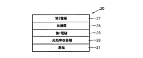
前述のような式(1)で表示される化合物を含んだ光効率改善層を具備した有機発光素子は、優れた光効率を達成する。 The organic light emitting device having the light efficiency improving layer containing the compound represented by the formula (1) as described above achieves excellent light efficiency.
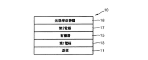
図1は、本発明の一具現例による有機発光素子10の断面図を概略的に図示したものである。 有機発光素子10は、基板11、第1電極13、有機層15、第2電極17及び光効率改善層18を順に具備する。前記第2電極17は透過型電極であって、有機層15で生成された光は、第2電極17を過ぎて光効率改善層18を通過し、有機発光素子10の外部に取り出されうる。 FIG. 1 is a schematic cross-sectional view of an organic light emitting device 10 according to an embodiment of the present invention. The organic light emitting device 10 includes a substrate 11, a first electrode 13, an organic layer 15, a second electrode 17, and a light efficiency improving layer 18 in order. The second electrode 17 is a transmissive electrode, and the light generated in the organic layer 15 passes through the second electrode 17 and passes through the light efficiency improving layer 18 and can be extracted outside the organic light emitting device 10.
前記基板11としては、一般的な有機発光素子で使われる基板を使用できるが、機械的強度、熱的安定性、透明性、表面平滑性、取扱容易性及び防水性にすぐれるガラス基板または透明プラスチック基板を使用できる。 As the substrate 11, a substrate used in a general organic light emitting device can be used, but a glass substrate or a transparent material excellent in mechanical strength, thermal stability, transparency, surface smoothness, ease of handling and waterproofness. Plastic substrates can be used.
前記第1電極13は、基板上部に第1電極用物質を蒸着法またはスパッタリング法などを利用して提供することによって形成されうる。前記第1電極13は、後述する有機層15と接触した第1面及び前記有機層15の反対側に位置した第2面を有する。前記第1電極13がアノードである場合、正孔注入が容易なように、第1電極用物質は、大きい仕事関数を有する物質のうちから選択されうる。前記第1電極13は、反射型電極または透過型電極でありうる。第1電極用の物質としては、透明であって伝導性にすぐれる酸化インジウムスズ(ITO)、酸化インジウム亜鉛(IZO)、酸化スズ(SnO2)、酸化亜鉛(ZnO)などを利用できる。または、マグネシウム(Mg)、アルミニウム(Al)、アルミニウム−リチウム(Al−Li)、カルシウム(Ca)、マグネシウム−インジウム(Mg−In)、マグネシウム−銀(Mg−Ag)などを利用すれば、前記第1電極13を反射型電極として形成することもできる。 The first electrode 13 may be formed by providing a first electrode material on the substrate using a deposition method or a sputtering method. The first electrode 13 has a first surface in contact with an organic layer 15 to be described later and a second surface located on the opposite side of the organic layer 15. When the first electrode 13 is an anode, the first electrode material may be selected from materials having a large work function so as to facilitate hole injection. The first electrode 13 may be a reflective electrode or a transmissive electrode. As the material for the first electrode, indium tin oxide (ITO), indium zinc oxide (IZO), tin oxide (SnO 2 ), zinc oxide (ZnO), etc., which are transparent and have excellent conductivity can be used. Alternatively, if magnesium (Mg), aluminum (Al), aluminum-lithium (Al-Li), calcium (Ca), magnesium-indium (Mg-In), magnesium-silver (Mg-Ag) or the like is used, The first electrode 13 can also be formed as a reflective electrode.
前記第1電極13の上部には、有機層15が備わっている。本明細書において、「有機層」とは、第1電極と第2電極との間に介在されたあらゆる層を包括して指すものであり、前記有機層は、金属錯体なども含むことができ、必ずしも有機物のみによってなる層を意味するものではない。 An organic layer 15 is provided on the first electrode 13. In this specification, the “organic layer” refers to all layers interposed between the first electrode and the second electrode, and the organic layer may include a metal complex or the like. However, it does not necessarily mean a layer made of only organic matter.
前記有機層15は、正孔注入層、正孔輸送層、発光層、正孔阻止層、電子輸送層及び電子注入層のうち、1層以上の層を含むことができる。 The organic layer 15 may include one or more layers among a hole injection layer, a hole transport layer, a light emitting layer, a hole blocking layer, an electron transport layer, and an electron injection layer.
正孔注入層(HIL)は、前記第1電極13の上部に、真空蒸着法、スピンコーティング法、キャスト法、LB(Langmuir‐Blodgett)法のような多様な方法を利用して形成されうる。 The hole injection layer (HIL) may be formed on the first electrode 13 using various methods such as vacuum deposition, spin coating, casting, and LB (Langmuir-Blodgett).
真空蒸着法によって正孔注入層を形成する場合、その蒸着条件は、正孔注入層の材料として使用する化合物、目的とする正孔注入層の構造及び熱的特性などによって異なるが、一般的に、蒸着温度100ないし500℃、真空度10−8ないし10−3torr、蒸着速度0.01ないし100Å/secの範囲で適切に選択することが望ましい。 When forming a hole injection layer by a vacuum deposition method, the deposition conditions differ depending on the compound used as the material of the hole injection layer, the structure of the target hole injection layer, the thermal characteristics, etc. It is desirable that the deposition temperature is appropriately selected in the range of 100 to 500 ° C., the degree of vacuum of 10 −8 to 10 −3 torr, and the deposition rate of 0.01 to 100 Å / sec.
スピンコーティング法によって正孔注入層を形成する場合、そのコーティング条件は、正孔注入層の材料として使用する化合物、目的するする正孔注入層の構造及び熱的特性によって異なるが、およそ2,000rpmないし5,000rpmのコーティング速度、コーティング後の溶媒除去のための熱処理温度は、およそ80℃ないし200℃の温度範囲で適切に選択することが望ましい。 When the hole injection layer is formed by the spin coating method, the coating conditions vary depending on the compound used as the material of the hole injection layer, the structure of the target hole injection layer, and the thermal characteristics, but approximately 2,000 rpm. The coating speed of 5,000 rpm and the heat treatment temperature for removing the solvent after coating are desirably selected appropriately within a temperature range of about 80 ° C. to 200 ° C.
正孔注入層物質としては、公知の正孔注入材料を使用でき、例えば、銅フタロシアニンのようなフタロシアニン化合物、4,4’,4’’−トリス(3−メチルフェニルフェニルアミノ)トリフェニルアミン(m−MTDATA)、N,N’−ジ(1−ナフチル)−N,N’−ジフェニルベンジジン(NPB)、TDATA、2T−NATA、ポリアニリン/ドデシルベンゼンスルホン酸(Pani/DBSA)、ポリ(3,4−エチレンジオキシチオフェン)/ポリ(4−スチレンスルホネート)(PEDOT/PSS)、ポリアニリン/カンファースルホン酸(Pani/CSA)またはポリアニリン/ポリ(4−スチレンスルホネート)(PANI/PSS)などを使用できるが、これらに限定されるものではない。いくつかの上記物質の構造を以下に示す。 As the hole injection layer substance, a known hole injection material can be used. For example, a phthalocyanine compound such as copper phthalocyanine, 4,4 ′, 4 ″ -tris (3-methylphenylphenylamino) triphenylamine ( m-MTDATA), N, N′-di (1-naphthyl) -N, N′-diphenylbenzidine (NPB), TDATA, 2T-NATA, polyaniline / dodecylbenzenesulfonic acid (Pani / DBSA), poly (3, 4-ethylenedioxythiophene) / poly (4-styrene sulfonate) (PEDOT / PSS), polyaniline / camphor sulfonic acid (Pani / CSA) or polyaniline / poly (4-styrene sulfonate) (PANI / PSS) can be used. However, it is not limited to these. The structures of some of the above materials are shown below.
前記正孔注入層の厚さは、およそ100Åないし10,000Å、望ましくは100Åないし1,000Åでありうる。前記正孔注入層の厚さが前述のような範囲を満足する場合、実質的な駆動電圧の上昇なしに満足すべきほどの正孔注入特性を得ることができる。 The hole injection layer may have a thickness of about 100 to 10,000, preferably about 100 to 1,000. When the thickness of the hole injection layer satisfies the above-described range, a sufficient hole injection characteristic can be obtained without a substantial increase in driving voltage.
次に、前記正孔注入層の上部に、真空蒸着法、スピンコーティング法、キャスト法、LB法のような多様な方法を利用して正孔輸送層(HTL)を形成できる。真空蒸着法及びスピンコーティング法によって正孔輸送層を形成する場合、その蒸着条件及びコーティング条件は、使用する化合物によって異なるが、一般的に、正孔注入層の形成とほぼ同じ条件範囲のうちから選択される。 Next, a hole transport layer (HTL) can be formed on the hole injection layer using various methods such as vacuum deposition, spin coating, casting, and LB. When forming a hole transport layer by a vacuum deposition method or a spin coating method, the deposition conditions and coating conditions vary depending on the compound used, but in general, from the same range of conditions as the formation of a hole injection layer. Selected.
正孔輸送層物質は、公知の正孔輸送材料を利用して形成でき、例えば、N−フェニルカルバゾール、ポリビニルカルバゾールのようなカルバゾール誘導体;N,N’−ビス(3−メチルフェニル)−N,N’−ジフェニル−[1,1−ビフェニル]−4,4’−ジアミン(TPD)、N,N’−ジ(ナフタレン−1−イル)−N,N’−ジフェニルベンジジン(α−NPD)のような芳香族縮合環を有するアミン誘導体;4,4’,4”−トリス(N−カルバゾリル)トリフェニルアミン(TCTA)のようなトリフェニルアミン系物質のような公知の正孔輸送物質を使用できる。このうち、例えば、TCTAの場合、正孔輸送の役割以外にも、発光層から励起子が広がることを防止する役割も行うことができる。いくつかの上記物質の構造を以下に示す。 The hole transport layer material can be formed using a known hole transport material, for example, carbazole derivatives such as N-phenylcarbazole and polyvinylcarbazole; N, N′-bis (3-methylphenyl) -N, N′-diphenyl- [1,1-biphenyl] -4,4′-diamine (TPD), N, N′-di (naphthalen-1-yl) -N, N′-diphenylbenzidine (α-NPD) Amine derivatives having such aromatic condensed rings; use of known hole transport materials such as triphenylamine-based materials such as 4,4 ′, 4 ″ -tris (N-carbazolyl) triphenylamine (TCTA) Among them, for example, in the case of TCTA, in addition to the role of hole transport, it can also play a role of preventing the exciton from spreading from the light emitting layer. It is shown below.
前記正孔輸送層の厚さは、およそ50Åないし1,000Å、望ましくは100Åないし800Åでありうる。前記正孔輸送層の厚さが前述のような範囲を満足する場合、実質的な駆動電圧の上昇なしに満足すべきほどの正孔輸送特性を得ることができる。
前記正孔輸送層の上部に、真空蒸着法、スピンコーティング法、キャスト法、LB法のような方法を利用して発光層(EML)を形成できる。真空蒸着法及びスピンコーティング法によって発光層を形成する場合、その蒸着条件は、使用する化合物によって異なるが、一般的に、正孔注入層の形成とほぼ同じ条件範囲のうちから選択される。
The hole transport layer may have a thickness of about 50 to 1,000 mm, preferably 100 to 800 mm. When the thickness of the hole transport layer satisfies the above range, satisfactory hole transport characteristics can be obtained without a substantial increase in driving voltage.
A light emitting layer (EML) can be formed on the hole transport layer using a method such as vacuum deposition, spin coating, casting, or LB. In the case of forming a light emitting layer by a vacuum deposition method or a spin coating method, the deposition conditions vary depending on the compound used, but are generally selected from the same range of conditions as the formation of the hole injection layer.
前記発光層は、一つの化合物を含むか、ホストとドーパントとの組み合わせを含むことができる。公知のホストの例としては、トリス(8−ヒドロキシキノリン)アルミニウム(Alq3)、4,4’−N,N’−ジカルバゾール−ビフェニル(CBP)、ポリ(n−ビニルカルバゾール)(PVK)、9,10−ジ(ナフタレン−2−イル)アントラセン(ADN)、TCTA、1,3,5−トリス(N−フェニルベンズイミダゾール−2−イル)ベンゼン(TPBI)、3−tert−ブチル−9,10−ジ(ナフト−2−イル)アントラセン(TBADN)、E3、ジスチリルアリーレン(DSA)などを使用できるが、これらに限定されるものではない。 The light emitting layer may include one compound or a combination of a host and a dopant. Examples of known hosts include tris (8-hydroxyquinoline) aluminum (Alq3), 4,4′-N, N′-dicarbazole-biphenyl (CBP), poly (n-vinylcarbazole) (PVK), 9 , 10-di (naphthalen-2-yl) anthracene (ADN), TCTA, 1,3,5-tris (N-phenylbenzimidazol-2-yl) benzene (TPBI), 3-tert-butyl-9,10 -Di (naphth-2-yl) anthracene (TBADN), E3, distyrylarylene (DSA) and the like can be used, but are not limited thereto.
一方、公知の赤色ドーパントとして、PtOEP、Ir(piq)3、Btp2Ir(acac)、4−(ジシアノメチレン)−2−tert-ブチル−6−(1,1,7,7−テトラメチルジュロリジン−4−イル−ビニル)−4H−ピラン(DCJTB)などを利用できるが、これらに限定されるものではない。 On the other hand, as known red dopants, PtOEP, Ir (piq) 3 , Btp 2 Ir (acac), 4- (dicyanomethylene) -2-tert-butyl-6- (1,1,7,7-tetramethyljuro Although lysine-4-yl-vinyl) -4H-pyran (DCJTB) can be used, it is not limited thereto.
また、公知の緑色ドーパントとして、Ir(ppy)3(ppy=フェニルピリジン)、Ir(ppy)2(acac)、Ir(mpyp)3、C545T(林原社製)などを利用できるが、これらに限定されるものではない。 Further, Ir (ppy) 3 (ppy = phenylpyridine), Ir (ppy) 2 (acac), Ir (mpyp) 3 , C545T (manufactured by Hayashibara Co., Ltd.) and the like can be used as known green dopants, but are not limited thereto. Is not to be done.
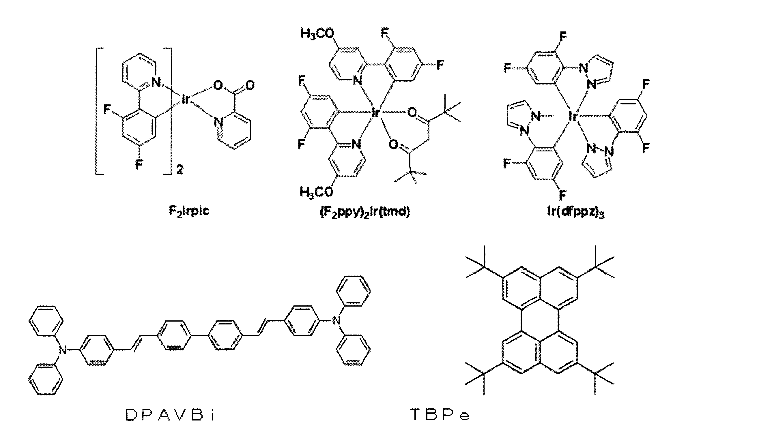
一方、公知の青色ドーパントとして、F2Irpic、(F2ppy)2Ir(tmd)、Ir(dfppz)3、ter−フルオレン、4,4’−ビス(4−ジフェニルアミノスチリル)ビフェニル(DPAVBi)、2,5,8,11−テトラ−t−ブチルフェリレン(TBPe)などを利用できるが、これらに限定されるものではない。 On the other hand, as known blue dopant, F 2 Irpic, (F 2 ppy) 2 Ir (tmd), Ir (dfppz) 3, ter- fluorene, 4,4'-bis (4-diphenylaminostyryl) biphenyl (DPAVBi) 2,5,8,11-tetra-t-butylferylene (TBPe) can be used, but is not limited thereto.
ドーパントとホストとを共に使用する場合、ドーパントのドーピング濃度は特別に制限されるものではないが、一般的に、ホスト100重量部を基準として、前記ドーパントの含有量は、0.01〜15重量部である。 When the dopant and the host are used together, the doping concentration of the dopant is not particularly limited, but generally, the dopant content is 0.01 to 15 weight based on 100 parts by weight of the host. Part.
前記発光層の厚さはおよそ100Åないし1,000Å、望ましくは200Åないし600Åでありうる。前記発光層の厚さが前述のような範囲を満足する場合、実質的な駆動電圧の上昇なしに優秀な発光特性を示すことができる。 The light emitting layer may have a thickness of about 100 to 1,000 mm, preferably 200 to 600 mm. When the thickness of the light emitting layer satisfies the above range, excellent light emission characteristics can be exhibited without a substantial increase in driving voltage.
発光層にリン光ドーパントを共に使用する場合には、三重項励起子または正孔が電子輸送層に広がる現象を防止するために、前記電子輸送層と発光層との間に、真空蒸着法、スピンコーティング法、キャスト法、LB法のような方法を利用し、正孔阻止層(HBL)を形成できる。真空蒸着法及びスピンコーティング法によって正孔阻止層を形成する場合、その条件は、使用する化合物によって異なるが、一般的に、正孔注入層の形成とほぼ同じ条件範囲のうちから選択される。公知の正孔阻止の材料も使用できるが、その例としては、オキサジアゾール誘導体やトリアゾール誘導体、フェナントロリン誘導体などを挙げることができる。 When using a phosphorescent dopant together in the light emitting layer, in order to prevent the phenomenon of triplet excitons or holes spreading to the electron transport layer, a vacuum deposition method between the electron transport layer and the light emitting layer, A hole blocking layer (HBL) can be formed using a method such as spin coating, casting, or LB. When the hole blocking layer is formed by the vacuum deposition method and the spin coating method, the conditions vary depending on the compound used, but are generally selected from the same range of conditions as the formation of the hole injection layer. Known hole blocking materials can also be used. Examples thereof include oxadiazole derivatives, triazole derivatives, and phenanthroline derivatives.
前記正孔阻止層の厚さは、およそ50Åないし1,000Å、望ましくは100Åないし300Åでありうる。前記正孔阻止層の厚さが前述のような範囲を満足する場合、実質的な駆動電圧の上昇なしに優秀な正孔阻止特性を得ることができる。 The hole blocking layer may have a thickness of about 50 to 1,000 mm, preferably 100 to 300 mm. When the thickness of the hole blocking layer satisfies the above range, excellent hole blocking characteristics can be obtained without a substantial increase in driving voltage.
次に、電子輸送層(ETL)を真空蒸着法、またはスピンコーティング法、キャスト法などの多様な方法を利用して形成する。真空蒸着法及びスピンコーティング法によって電子輸送層を形成する場合、その条件は、使用する化合物によって異なるが、一般的に、正孔注入層の形成とほぼ同じ条件範囲のうちから選択される。前記電子輸送層の材料は、電子注入電極(カソード)から注入された電子を安定的に輸送する機能を行うものであり、公知の電子輸送物質を利用できる。その例としては、キノリン誘導体、特に、Alq3、下記に示すTAZ、Balqのような公知の材料を使用することができるが、これらに限定されるものではない。 Next, an electron transport layer (ETL) is formed using various methods such as vacuum deposition, spin coating, and casting. When an electron transport layer is formed by a vacuum deposition method or a spin coating method, the conditions vary depending on the compound used, but are generally selected from the same range of conditions as the formation of a hole injection layer. The material of the electron transport layer performs a function of stably transporting electrons injected from the electron injection electrode (cathode), and a known electron transport material can be used. Examples thereof include, but are not limited to, quinoline derivatives, particularly Alq3, known materials such as TAZ and Balq shown below.
前記電子輸送層の厚さは、およそ100Åないし1,000Å、望ましくは150Åないし500Åでありうる。前記電子輸送層の厚さが前述のような範囲を満足する場合、実質的な駆動電圧の上昇なしに満足すべきほどの電子輸送特性を得ることができる。 The electron transport layer may have a thickness of about 100 to 1,000 mm, preferably 150 to 500 mm. When the thickness of the electron transport layer satisfies the above-mentioned range, satisfactory electron transport characteristics can be obtained without a substantial increase in driving voltage.
また、電子輸送層の上部に、カソードから電子の注入を容易にする機能を有する物質である電子注入層(EIL)が積層されうるが、これは、特別に材料を制限するものではない。 In addition, an electron injection layer (EIL), which is a substance having a function of facilitating electron injection from the cathode, may be stacked on the electron transport layer, but this does not limit the material.
前記電子注入層の形成材料としては、LiF、NaCl、CsF、Li2O、BaOのような電子注入層の形成材料であって、公知の任意の物質を利用できる。前記電子注入層の蒸着条件は、使用する化合物によって異なるが、一般的に、正孔注入層の形成とほぼ同じ条件範囲のうちから選択される。 As a material for forming the electron injection layer, a material for forming an electron injection layer such as LiF, NaCl, CsF, Li 2 O, or BaO can be used. The deposition conditions for the electron injection layer vary depending on the compound used, but are generally selected from the same range of conditions as the formation of the hole injection layer.
前記電子注入層の厚さはおよそ1Åないし100Å、望ましくは5Åないし90Åでありうる。前記電子注入層の厚さが前述のような範囲を満足する場合、実質的な駆動電圧の上昇なしに満足すべきほどの電子注入特性を得ることができる。 The electron injection layer may have a thickness of about 1 to 100 mm, preferably 5 to 90 mm. When the thickness of the electron injection layer satisfies the above-described range, it is possible to obtain satisfactory electron injection characteristics without a substantial increase in driving voltage.
かような有機層15の上部には、透過型電極である第2電極17が備わっている。前記第2電極17は、前記有機層15と接した第1面と前記有機層15の反対側に位置した第2面とを有する。前記第2電極17は、電子注入電極であるカソードであるが、このとき、前記第2電極形成用の金属としては、小さい仕事関数を有する金属、合金、電気伝導性化合物及びそれらの混合物を使用できる。具体的な例としては、リチウム(Li)、マグネシウム(Mg)、アルミニウム(Al)、アルミニウム−リチウム(Al−Li)、カルシウム(Ca)、マグネシウム−インジウム(Mg−In)、マグネシウム−銀(Mg−Ag)など薄膜に形成して透過型電極を得ることができる。一方、前面発光素子を得るために、ITO、IZOを利用した透過型電極を形成できるなど、多様な変形が可能である。 A second electrode 17 that is a transmission electrode is provided on the organic layer 15. The second electrode 17 has a first surface in contact with the organic layer 15 and a second surface located on the opposite side of the organic layer 15. The second electrode 17 is a cathode that is an electron injection electrode. At this time, a metal having a small work function, an alloy, an electrically conductive compound, and a mixture thereof are used as the metal for forming the second electrode. it can. Specific examples include lithium (Li), magnesium (Mg), aluminum (Al), aluminum-lithium (Al-Li), calcium (Ca), magnesium-indium (Mg-In), magnesium-silver (Mg). -Ag) can be formed into a thin film to obtain a transmission electrode. On the other hand, in order to obtain a front light emitting element, various modifications such as formation of a transmission electrode using ITO or IZO are possible.
本発明の一の実施態様において、 前記第2電極17の第2面の上部には、光効率改善層18が備わっている。前記光効率改善層18は、下記式(1)で表示される化合物を含む: In one embodiment of the present invention, a light efficiency improving layer 18 is provided on the second surface of the second electrode 17. The light efficiency improving layer 18 includes a compound represented by the following formula (1):
具体的に、前記式(1)で、X1,X3及びX5がNであるか、またはX1,X3及びX4がNであるか、またはX1及びX3がNであるか、またはX1及びX4がNであるか、またはX1がNであるが、これらに限定されるものではない。 Specifically, in the formula (1), X 1 , X 3 and X 5 are N, or X 1 , X 3 and X 4 are N, or X 1 and X 3 are N Or X 1 and X 4 are N, or X 1 is N, but is not limited thereto.
さらに具体的に、前記式(1)で表示される化合物は、下記化学式1aないし1eのうち、いずれか一つの構造を有することができるが、これらに限定されるものではない: More specifically, the compound represented by the formula (1) may have any one structure among the following chemical formulas 1a to 1e, but is not limited thereto:
前記式(1)で、Ar1ないしAr6は、互いに独立に、置換または非置換のC5−C30アリーレン基または置換または非置換のC2−C30ヘテロアリーレン基でありうる。 In the formula (1), Ar 1 to Ar 6 may each independently be a substituted or unsubstituted C 5 -C 30 arylene group or a substituted or unsubstituted C 2 -C 30 heteroarylene group.
具体的に、前記Ar1ないしAr6は、互いに独立に、置換または非置換のフェニレン基、置換または非置換のペンタレニレン基、置換または非置換のインデニレン基、置換または非置換のナフチレン基、置換または非置換のアズレニレン基、置換または非置換のヘプタレニレン基、置換または非置換のインダセニレン基、置換または非置換のアセナフチレニレン基、置換または非置換のフルオレニレン基、置換または非置換のフェナレニレン基、置換または非置換のフェナントレニレン基、置換または非置換のアントラセニレン基、置換または非置換のフルオランテニレン基、置換または非置換のトリフェニレニレン基、置換または非置換のピレニレン基、置換または非置換のクリセニレン基、置換または非置換のナフタセニレン基、置換または非置換のピセニレン基、置換または非置換のペリレニレン基、置換または非置換のペンタフェニレン基、置換または非置換のヘキサセニレン基、置換または非置換のピロリレン基、置換または非置換のピラゾリレン基、置換または非置換のイミダゾリレン基、置換または非置換のイミダゾリニレン基、置換または非置換のピリジニレン基、置換または非置換のピラジニレン基、置換または非置換のピリミジニレン基、置換または非置換のインドリレン基、置換または非置換のプリニレン基、置換または非置換のキノリニレン基、置換または非置換のフタラジニレン基、置換または非置換のインドリジニレン基、置換または非置換のナフチリジニレン基、置換または非置換のキナゾリニレン基、置換または非置換のシノリニレン基、置換または非置換のインダゾリレン基、置換または非置換のカルバゾリレン基、置換または非置換のフェナジニレン基、置換または非置換のフェナントリジニレン基、置換または非置換のピラニレン基、置換または非置換のクロメニレン基、置換または非置換のベンゾフラニレン基、置換または非置換のチオフェニレン基、置換または非置換のベンゾチオフェニレン基、置換または非置換のイソチアゾリレン基、置換または非置換のイソキサゾリレン基または置換または非置換のトリアゾリレン基からなる群から選択されうる。 Specifically, Ar 1 to Ar 6 are each independently a substituted or unsubstituted phenylene group, a substituted or unsubstituted pentalenylene group, a substituted or unsubstituted indenylene group, a substituted or unsubstituted naphthylene group, substituted or unsubstituted Unsubstituted azulenylene group, substituted or unsubstituted heptalenylene group, substituted or unsubstituted indasenylene group, substituted or unsubstituted acenaphthyleneylene group, substituted or unsubstituted fluorenylene group, substituted or unsubstituted phenalenylene group, substituted Or unsubstituted phenanthrenylene group, substituted or unsubstituted anthracenylene group, substituted or unsubstituted fluoranthenylene group, substituted or unsubstituted triphenylenylene group, substituted or unsubstituted pyrenylene group, substituted or unsubstituted A chrysenylene group, a substituted or unsubstituted naphthacenylene group, Or an unsubstituted picenylene group, a substituted or unsubstituted peryleneylene group, a substituted or unsubstituted pentaphenylene group, a substituted or unsubstituted hexasenylene group, a substituted or unsubstituted pyrrolylene group, a substituted or unsubstituted pyrazolylene group, substituted or Unsubstituted imidazolylene group, substituted or unsubstituted imidazolinylene group, substituted or unsubstituted pyridinylene group, substituted or unsubstituted pyrazinylene group, substituted or unsubstituted pyrimidinylene group, substituted or unsubstituted indylene group, substituted or unsubstituted Plinylene group, substituted or unsubstituted quinolinylene group, substituted or unsubstituted phthalazinylene group, substituted or unsubstituted indolizinylene group, substituted or unsubstituted naphthyridinylene group, substituted or unsubstituted quinazolinylene group, substituted or unsubstituted A sinolinylene group, substitution Or an unsubstituted indazolylene group, a substituted or unsubstituted carbazolylene group, a substituted or unsubstituted phenazinylene group, a substituted or unsubstituted phenanthridinylene group, a substituted or unsubstituted pyranylene group, a substituted or unsubstituted chromenylene group, Substituted or unsubstituted benzofuranylene group, substituted or unsubstituted thiophenylene group, substituted or unsubstituted benzothiophenylene group, substituted or unsubstituted isothiazolylene group, substituted or unsubstituted isoxazolylene group or substituted or unsubstituted triazolylene group Can be selected from the group consisting of
一方、前記Ar1ないしAr6は、前述のように、非置換のC5−C30アリーレン基または非置換のC2−C30ヘテロアリーレン基以外に、置換されたC5−C30アリーレン基または置換されたC2−C30ヘテロアリーレン基でありうる。置換されたC5−C30芳香族環システムまたは置換されたC2−C30ヘテロ芳香族環システムにおける一つ以上の置換基は、互いに独立に、ハロゲン原子、ヒドロキシ基、シアノ基、置換または非置換のC1−C30アルキル基、置換または非置換のC1−C30アルコキシ基、置換または非置換のC1−C30アシル基、置換または非置換のC2−C30アルケニル基、置換または非置換のC2−C30アルキニル基、置換または非置換のC5−C30アリール基または置換または非置換のC2−C30ヘテロアリール基でありうる。ここで、システムとは、縮合環、非縮合環、及び、少なくとも2つ以上の縮合環、非縮合環もしくはこれらの組合わせが、一重結合もしくは二重結合で直結された環集合を意味し、以下において同様である。 Meanwhile, the Ar 1 through Ar 6, as described above, in addition to unsubstituted C 5 -C 30 arylene group or unsubstituted C 2 -C 30 heteroarylene group, substituted C 5 -C 30 arylene group or it may be substituted C 2 -C 30 hetero arylene group. One or more substituents in a substituted C 5 -C 30 aromatic ring system or a substituted C 2 -C 30 heteroaromatic ring system are independently of one another halogen atoms, hydroxy groups, cyano groups, substituted or unsubstituted C 1 -C 30 alkyl group, a substituted or unsubstituted C 1 -C 30 alkoxy group, a substituted or unsubstituted C 1 -C 30 acyl group, a substituted or unsubstituted C 2 -C 30 alkenyl group, substituted or unsubstituted C 2 -C 30 alkynyl group may be a substituted or unsubstituted C 5 -C 30 aryl group or a substituted or unsubstituted C 2 -C 30 heteroaryl group. Here, the system means a condensed ring, a non-condensed ring, and a ring assembly in which at least two or more condensed rings, a non-fused ring or a combination thereof is directly connected by a single bond or a double bond, The same applies to the following.
具体的に、前記置換基は、ハロゲン原子、ヒドロキシ基、シアノ基、C1−C10アルキル基、C1−C10アルコキシ基、C1−C10アシル基、C2−C10アルケニル基、C2−C10アルキニル基、C5−C14 アリール基またはC2−C14ヘテロアリール基でありうる。 Specifically, the substituent include a halogen atom, hydroxy group, cyano groups, C 1 -C 10 alkyl group, C 1 -C 10 alkoxy group, C 1 -C 10 acyl group, C 2 -C 10 alkenyl group, C 2 -C 10 alkynyl group, it may be a C5-C14 aryl group or C2-C14 heteroaryl group.
さらに具体的に、前記Ar1ないしAr6は、互いに独立に、フェニレン基、一つ以上のシアノ基で置換されたフェニレン基、一つ以上のC1−C10アルキル基で置換されたフェニレン基、ナフチレン基、一つ以上のシアノ基で置換されたナフチレン基、一つ以上のC1−C10アルキル基で置換されたナフチレン基、フルオレニレン基、一つ以上のC1−C10アルキル基で置換されたフルオレニレン基、カルバゾリレン基、一つ以上のフェニル基で置換されたカルバゾリレン基、ピリジニレン基、トリアゾリレン基、または一つ以上のフェニル基で置換されたトリアゾリレン基でありうる。 More specifically, the Ar 1 to Ar 6 are independently of each other a phenylene group, a phenylene group substituted with one or more cyano groups, or a phenylene group substituted with one or more C 1 -C 10 alkyl groups. A naphthylene group, a naphthylene group substituted with one or more cyano groups, a naphthylene group substituted with one or more C 1 -C 10 alkyl groups, a fluorenylene group, one or more C 1 -C 10 alkyl groups It can be a substituted fluorenylene group, a carbazolylene group, a carbazolylene group substituted with one or more phenyl groups, a pyridinylene group, a triazolylene group, or a triazolylene group substituted with one or more phenyl groups.
前記Ar1ないしAr6は、互いに独立に、下記化学式2aないし2pのうち、いずれか一つであるが、これに限定されるものではない: Ar 1 to Ar 6 are each independently one of the following chemical formulas 2a to 2p, but are not limited thereto:
前記化学式で、*は、式(1)に図示された6員芳香族環元素であるCとの連結サイトであり、*’は、R1ないしR6のうち、一つとの連結サイトである。 In the above chemical formula, * is a connecting site with C, which is the 6-membered aromatic ring element illustrated in Formula (1), and * ′ is a connecting site with one of R 1 to R 6. .
前記式(1)で、a,b,c,d,e及びfは、Ar1ないしAr6の反復回数を示したものであり、0ないし10の整数でありうる。a,b,c,d,e及びfが互いに独立的に0である場合、R1ないしR6が式(1)に図示された6員芳香族環の環元素と直接連結されうる。一方、aが2以上である場合、2以上のAr1は、互いに同一であるか、または異なり、bが2以上である場合、2以上のAr2は、互いに同一であるか、または異なり、cが2以上である場合、2以上のAr3は、互いに同一であるか、または異なり、dが2以上である場合、2以上のAr4は、互いに同一であるか、または異なり、eが2以上である場合、2以上のAr5は、互いに同一であるか、または異なり、fが2以上である場合、2以上のAr6は、互いに同一であるか、または異なりうる。具体的に、a,b,c,d,e及びfは、互いに独立に、0,1,2または3であり、特に、1、2または3である。 In the formula (1), a, b, c, d, e and f represent the number of repetitions of Ar 1 to Ar 6 and may be integers of 0 to 10. When a, b, c, d, e and f are 0 independently of each other, R 1 to R 6 can be directly connected to the ring element of the 6-membered aromatic ring shown in Formula (1). On the other hand, when a is 2 or more, two or more Ar 1 are the same or different from each other, and when b is two or more, two or more Ar 2 are the same or different from each other, When c is 2 or more, two or more Ar 3 are the same or different from each other, and when d is two or more, two or more Ar 4 are the same or different from each other, and e is When two or more, two or more Ar 5 may be the same or different from each other, and when f is two or more, two or more Ar 6 may be the same or different from each other. Specifically, a, b, c, d, e, and f are independently 0, 1, 2, or 3, and in particular, 1, 2, or 3.
前記式(1)で、R1ないしR6は、互いに独立に、水素、ハロゲン原子、ヒドロキシ基、シアノ基、置換または非置換のC1−C30アルキル基、置換または非置換のC1−C30アルコキシ基、置換または非置換のC1−C30アシル基、置換または非置換のC2−C30アルケニル基、置換または非置換のC2−C30アルキニル基、置換または非置換のC5−C30アリール基または置換または非置換のC2−C30ヘテロアリール基でありうる。このとき、前記R1ないしR6のうち、隣接した2以上は互いに結合し、飽和または不飽和環を形成できる。 In the formula (1), R 1 to R 6 are independently of each other hydrogen, halogen atom, hydroxy group, cyano group, substituted or unsubstituted C 1 -C 30 alkyl group, substituted or unsubstituted C 1- C 30 alkoxy group, a substituted or unsubstituted C 1 -C 30 acyl group, a substituted or unsubstituted C 2 -C 30 alkenyl group, a substituted or unsubstituted C 2 -C 30 alkynyl group, a substituted or unsubstituted C It may be 5 -C 30 aryl group or a substituted or unsubstituted C 2 -C 30 heteroaryl group. At this time, two or more adjacent R 1 to R 6 may be bonded to each other to form a saturated or unsaturated ring.
具体的に、前記R1ないしR6は、互いに独立に、水素、ハロゲン原子、ヒドロキシ基、シアノ基、置換または非置換のC1−C10アルキル基、置換または非置換のC1−C10アルコキシ基、置換または非置換のC1−C10アシル基、置換または非置換のC2−C10アルケニル基、置換または非置換のC2−C10アルキニル基、置換または非置換のC5−C14 アリール基または置換または非置換のC2−C14 ヘテロアリール基でありうる。 Specifically, R 1 to R 6 are independently of each other hydrogen, halogen atom, hydroxy group, cyano group, substituted or unsubstituted C 1 -C 10 alkyl group, substituted or unsubstituted C 1 -C 10. alkoxy group, a substituted or unsubstituted C 1 -C 10 acyl group, a substituted or unsubstituted C 2 -C 10 alkenyl group, a substituted or unsubstituted C 2 -C 10 alkynyl group, a substituted or unsubstituted C 5 - It can be a C 14 aryl group or a substituted or unsubstituted C 2 -C 14 heteroaryl group.
さらに具体的に、前記R1ないしR6は、互いに独立に、ハロゲン原子、ヒドロキシ基、シアノ基、C1−C10アルキル基、C5−C14アリール基、シアノ基で置換されたC5−C14アリール基、一つ以上のC1−C10アルキル基で置換されたC5−C14アリール基、C2−C14ヘテロアリール基、シアノ基で置換されたC2−C14ヘテロアリール基、一つ以上のC1−C10アルキル基で置換されたC2−C14ヘテロアリール基、一つ以上のフェニル基で置換されたC2−C14ヘテロアリール基でありうる。 More specifically, the R 1 to R 6 are, independently of one another, a halogen atom, hydroxy group, cyano groups, C 1 -C 10 alkyl group, C 5 -C 14 aryl group, C 5 substituted with a cyano group -C 14 aryl group, one or more C 1 -C 10 alkyl C 5 -C 14 aryl group substituted with a group, C 2 -C 14 heteroaryl group, C 2 -C 14 heteroaryl which is substituted with a cyano group aryl group, may be one or more C 1 -C 10 alkyl C 2 -C 14 hetero aryl group substituted with a group, one or more C 2 -C 14 substituted with a phenyl group heteroaryl group.
前記R1ないしR6は、互いに独立に、水素であるか、または下記化学式3aないし3qのうち、いずれか一つであるが、これらに限定されるものではない: R 1 to R 6 are each independently hydrogen or any one of the following chemical formulas 3a to 3q, but are not limited thereto:
前記化学式で、*は、式(1)の6員芳香族環元素のC、またはAr1ないしAr6のうち一つとの連結サイトである。 In the chemical formula, * is a connecting site with C of the six-membered aromatic ring element of the formula (1) or one of Ar1 to Ar6.
また、前記式(1)で、−(Ar1)a−R1で表示される基、−(Ar2)b−R2で表示される基、−(Ar3)c−R3で表示される基、−(Ar4)d−R4で表示される基、−(Ar5)e−R5で表示される基、及び−(Ar6)f−R6で表示される基が、互いに独立に、下記化学式4aないし4yのうち一つであるが、これらに限定されるものではない: In the formula (1), a group represented by-(Ar 1 ) a -R 1 , a group represented by-(Ar 2 ) b -R 2 , and a group represented by-(Ar 3 ) c -R 3 A group represented by — (Ar 4 ) d —R 4 , a group represented by — (Ar 5 ) e —R 5 , and a group represented by — (Ar 6 ) f —R 6. Independently of each other, it is one of the following chemical formulas 4a to 4y, but is not limited thereto:
本発明の一実施態様によれば、式(1)で表示される化合物は前記化学式1aないし1eのうち一つで表され、このうちAr1ないしAr6は、互いに独立して、化学式2aないし2pで表される基のうち一つであり、R1ないしR6は、互いに独立して、水素であるか、または化学式3aないし3qで表される基のうち一つであり、aないしfは0ないし3の整数である。該式(1)で表示される化合物の非制限的な例は、下記化合物1ないし35のうち、いずれか一つでありうる: According to one embodiment of the present invention, the compound represented by the formula (1) is represented by one of the chemical formulas 1a to 1e, wherein Ar 1 to Ar 6 are independently of each other, the chemical formulas 2a to 2e. Each of R 1 to R 6 is independently hydrogen, or one of the groups represented by Chemical Formulas 3a to 3q, and a to f Is an integer from 0 to 3. Non-limiting examples of the compound represented by the formula (1) may be any one of the following compounds 1 to 35:
本明細書で、非置換のC1−C30アルキル基の具体的な例としては、メチル、エチル、プロピル、イソブチル、sec−ブチル、ペンチル、iso−アミル、ヘキシルなどを挙げることができ、前記アルキル基のうち一つ以上の水素原子は、ハロゲン原子、ヒドロキシ基、ニトロ基、シアノ基、アミノ基、アミジノ基、ヒドラジン、ヒドラゾン、カルボン酸基やその塩、スルホン酸基やその塩、リン酸やその塩、またはC1−C30アルキル基、C1−C30アルケニル基、C1−C30アルキニル基、C6−C30アリール基、C7−C20アリールアルキル基、C2−C20ヘテロアリール基またはC3−C30ヘテロアリールアルキル基で置換されうる。 Herein, specific examples of C 1 -C 30 alkyl group unsubstituted there may be mentioned methyl, ethyl, propyl, isobutyl, sec- butyl, pentyl, iso- amyl, hexyl and the like, the One or more hydrogen atoms in the alkyl group are a halogen atom, a hydroxy group, a nitro group, a cyano group, an amino group, an amidino group, a hydrazine, a hydrazone, a carboxylic acid group or a salt thereof, a sulfonic acid group or a salt thereof, or a phosphoric acid. and a salt thereof, or C 1 -C 30 alkyl group, C 1 -C 30 alkenyl group, C 1 -C 30 alkynyl, C 6 -C 30 aryl group, C 7 -C 20 arylalkyl group,, C 2 -C It can be substituted with 20 heteroaryl groups or C3-C30 heteroarylalkyl groups.
本明細書で、非置換のC1−C30アルコキシ基は、−OA(ただし、Aは、前述のようなC1−C30アルキル基である)の化学式を有し、この具体的な例として、メトキシ、エトキシ、イソプロピルオキシなどがあり、これらアルコキシ基のうち少なくとも一つ以上の水素原子は、前述のアルキル基の場合と同様な置換基で置換可能である。 Herein, C 1 -C 30 alkoxy group unsubstituted, -OA (although, A is a is C 1 -C 30 alkyl group as described above) has the chemical formula, the specific example As examples thereof, methoxy, ethoxy, isopropyloxy and the like, and at least one or more hydrogen atoms among these alkoxy groups can be substituted with the same substituents as in the case of the aforementioned alkyl groups.
本明細書で、非置換のC1−C30アシル基の具体的な例として、アセチル、エチルカルボニル、イソプロピルカルボニル、フェニルカルボニル、ナフチレンカルボニル、ジフェニルカルボニル、シクロヘキシルカルボニルなどがあり、それらアシル基のうち少なくとも一つ以上の水素原子は、前述のアルキル基の場合と同様な置換基で置換可能である。 In the specification, concrete examples of C 1 -C 30 acyl group unsubstituted acetyl, ethylcarbonyl, isopropylcarbonyl, phenylcarbonyl, naphthylene carbonyl, diphenyl carbonyl, include cyclohexylcarbonyl, their acyl group Among these, at least one or more hydrogen atoms can be substituted with the same substituent as in the case of the aforementioned alkyl group.
本明細書で、非置換のC2−C30アルケニル基は、前記定義されたようなアルキル基の中間や最末端に炭素二重結合を含有していることを意味する。例えば、エテニル、プロペニル、ブテニルなどがある。これらアルケニル基のうち少なくとも一つ以上の水素原子は、前述のアルキル基の場合と同様な置換基で置換可能である。 Herein, C 2 -C 30 alkenyl group unsubstituted means that contains a carbon-carbon double bond in the center or end alkyl group as previously defined. Examples include ethenyl, propenyl, butenyl and the like. Among these alkenyl groups, at least one hydrogen atom can be substituted with the same substituent as in the above-described alkyl group.
本明細書で、非置換のC2−C30アルキニル基は、前記定義されたようなアルキル基の中間や最末端に炭素三重結合を含有していることを意味する例としては、アセチレン、プロピレン、フェニルアセチレン、ナフチルアセチレン、イソプロピルアセチレン、t−ブチルアセチレン、ジフェニルアセチレンなどがある。これらアルキニル基のうち少なくとも一つ以上の水素原子は、前述のアルキル基の場合と同様な置換基で置換可能である。 In the present specification, an unsubstituted C 2 -C 30 alkynyl group includes a carbon triple bond in the middle or the most terminal of the alkyl group as defined above, and examples thereof include acetylene, propylene , Phenylacetylene, naphthylacetylene, isopropylacetylene, t-butylacetylene, diphenylacetylene, and the like. Among these alkynyl groups, at least one hydrogen atom can be substituted with the same substituent as in the case of the aforementioned alkyl group.
本明細書で、非置換のC5−C30アリール基は、一つ以上の芳香族環を含むC5−C30炭素環芳香族システムを有する一価基を意味し、非置換のC5−C30アリーレン基は、一つ以上の芳香族環を含むC5−C30炭素環芳香族システムを有する二価基を意味する。前記アリール基及びアリーレン基が2以上の環を含む場合、2以上の環は、互いに融合(fused)されるか、単一結合などを介して連結されうる。前記アリール基及びアリーレン基のうち一つ以上の水素原子は、前述のアルキル基の場合と同様な置換基で置換可能である。 Herein, C 5 -C 30 aryl group unsubstituted refers to a monovalent group having a C 5 -C 30 carbocyclic aromatic system containing at least one aromatic ring, unsubstituted C 5 A —C 30 arylene group refers to a divalent group having a C 5 -C 30 carbocyclic aromatic system containing one or more aromatic rings. When the aryl group and the arylene group include two or more rings, the two or more rings may be fused to each other or connected through a single bond or the like. One or more hydrogen atoms of the aryl group and arylene group can be substituted with the same substituent as in the case of the aforementioned alkyl group.
前記置換または非置換のC5−C30アリール基の例としては、フェニル基、C1−C10アルキルフェニル基(例えば、エチルフェニル基)、C1−C10アルキルビフェニル基(例えば、エチルビフェニル基)、ハロフェニル基(例えば、o−,m−及びp−フルオロフェニル基、ジクロロフェニル基)、ジシアノフェニル基、トリフルオロメトキシフェニル基、o−,m−及びp−トリル基、o−,m−及びp−クメニル基、メシチル基、フェノキシフェニル基、(α,α−ジメチルベンゼン)フェニル基、(N,N’−ジメチル)アミノフェニル基、(N,N’−ジフェニル)アミノフェニル基、ペンタレニル基、インデニル基、ナフチル基、ハロナフチル基(例えば、フルオロナフチル基)、C1−C10アルキルナフチル基(例えば、メチルナフチル基)、C1−C10アルコキシナフチル基(例えば、メトキシナフチル基)、アントラセニル基、アズレニル基、ヘプタレニル基、アセナフチレニル基、フェナレニル基、フルオレニル基、アントラキノリル基、メチルアントリル基、フェナントリル基、トリフェニレン基、ピレニル基、クリセニル基、エチル−クリセニル基、ピセニル基、ペリレニル基、クロロペリレニル基、ペンタフェニル基、ペンタセニル基、テトラフェニレニル基、ヘキサフェニル基、ヘキサセニル基、ルビセニル基、コロネリル基、トリナフチレニル基、ヘプタフェニル基、ヘプタセニル基、ピラントレニル基、オバレニル基などを挙げることができる。前記置換または非置換のC5−C30アリーレン基の例は、前記置換または非置換のC5−C30アリーレン基の例を参照して容易に認識されうる。 Examples C 5 -C 30 aryl group of said substituted or unsubstituted phenyl group, C 1 -C 10 alkylphenyl group (for example, ethylphenyl group), C 1 -C 10 alkyl biphenyl group (e.g., ethylbiphenyl Group), halophenyl group (for example, o-, m- and p-fluorophenyl group, dichlorophenyl group), dicyanophenyl group, trifluoromethoxyphenyl group, o-, m- and p-tolyl group, o-, m- And p-cumenyl group, mesityl group, phenoxyphenyl group, (α, α-dimethylbenzene) phenyl group, (N, N′-dimethyl) aminophenyl group, (N, N′-diphenyl) aminophenyl group, pentalenyl group , indenyl group, naphthyl group, a halonaphthyl group (such as fluoro naphthyl group), C 1 -C 10 alkyl naphthyl group For example, methylnaphthyl groups), C 1 -C 10 alkoxynaphthyl group (for example, methoxynaphthyl group), an anthracenyl group, an azulenyl group, heptalenyl group, an acenaphthylenyl group, a phenalenyl group, a fluorenyl group, an anthraquinolyl group, a methyl anthryl group, phenanthryl Group, triphenylene group, pyrenyl group, chrysenyl group, ethyl-chrysenyl group, picenyl group, perylenyl group, chloroperenyl group, pentaphenyl group, pentacenyl group, tetraphenylenyl group, hexaphenyl group, hexacenyl group, rubicenyl group, coronyl group , Trinaphthylenyl group, heptaphenyl group, heptacenyl group, pyrantrenyl group, and oberenyl group. Example C 5 -C 30 arylene group of said substituted or unsubstituted, may be easily recognized with reference to the example C 5 -C 30 arylene group of said substituted or unsubstituted.
本明細書で、非置換のC2−C30ヘテロアリール基は、N,O,PまたはSのうちから選択された1個以上のヘテロ原子を含み、残りの環原子がCである一つ以上の芳香族環からなるシステムを有する一価基を意味し、非置換のC2−C30ヘテロアリーレン基は、N,O,PまたはSのうちから選択された1個以上のヘテロ原子を含み、残りの環原子がCである一つ以上の芳香族環からなるシステムを有する二価基を意味する。ここで、前記ヘテロアリール基及びヘテロアリーレン基が2以上の環を含む場合、2以上の環は、互いに融合されたり、または単一結合などを介して連結されうる。前記ヘテロアリール基及びヘテロアリーレン基のうち一つ以上の水素原子は、前述のアルキル基の場合と同様な置換基で置換可能である。 One herein, C 2 -C 30 heteroaryl group unsubstituted comprises N, O, one or more hetero atoms selected from among P, or S, the remaining ring atoms being C Means a monovalent group having a system comprising the above aromatic rings, and the unsubstituted C 2 -C 30 heteroarylene group comprises one or more heteroatoms selected from N, O, P or S; Means a divalent group having a system consisting of one or more aromatic rings, wherein the remaining ring atom is C. Here, when the heteroaryl group and the heteroarylene group include two or more rings, the two or more rings may be fused to each other or connected through a single bond or the like. One or more hydrogen atoms of the heteroaryl group and heteroarylene group can be substituted with the same substituent as in the case of the aforementioned alkyl group.
前記非置換のC2−C30ヘテロアリール基の例には、ピラゾリル基、イミダゾリル基、オキサゾリル基、チアゾリル基、トリアゾリル基、テトラゾリル基、オキサジアゾリル基、ピリジニル基、ピリダジニル基、ピリミジニル基、トリアジニル基、カルバゾリル基、インドリル基、キノリニル基、イソキノリニル基などを挙げることができる。前記非置換のC2−C30ヘテロアリーレン基の例は、前記置換または非置換のC5−C30アリーレン基の例を参照して容易に認識されうる。 Examples of the unsubstituted C 2 -C 30 heteroaryl group include pyrazolyl group, imidazolyl group, oxazolyl group, thiazolyl group, triazolyl group, tetrazolyl group, oxadiazolyl group, pyridinyl group, pyridazinyl group, pyrimidinyl group, triazinyl group, A carbazolyl group, an indolyl group, a quinolinyl group, an isoquinolinyl group, and the like can be given. The examples of unsubstituted C 2 -C 30 heteroarylene group may be easily derived from examples C 5 -C 30 arylene group of said substituted or unsubstituted.
前記式(1)で表示される化合物は、公知の多様な方法を利用して製造可能であり、これは、当業者に容易に認識可能である。 The compound represented by the formula (1) can be produced using various known methods, which can be easily recognized by those skilled in the art.
前述のような式(1)で表示される化合物を含んだ光効率改善層18は、高い屈折率を有しており、有機発光素子の光効率、特に、外部発光効率向上に寄与できる。例えば、前記光効率改善層は、630nmの波長で1.8以上、望ましくは1.9の屈折率を有することができる。 The light efficiency improving layer 18 containing the compound represented by the formula (1) as described above has a high refractive index, and can contribute to improving the light efficiency of the organic light emitting device, particularly the external light emitting efficiency. For example, the light efficiency improving layer may have a refractive index of 1.8 or more, preferably 1.9 at a wavelength of 630 nm.
有機発光素子は、一般的に多様な材料からなる多層が積層された構造を有するために、有機層で生成された光が素子内のさまざまな層を通過しつつ、全反射によって、有機発光素子の外部の空気中に取り出されずに素子内で消滅しうる。このように、有機発光素子の外部に取り出される効率である外部発光効率が低い場合、有機層内での光変換効率が高くても、有機発光素子の全体光効率は低下しうる。しかし、前記光効率改善層18は、有機層15で生成された光が第2電極17を過ぎて空気中に進むとき、補強干渉の原理によって、有機発光素子の外部に取り出される効率を上昇させることができるので、有機発光素子の光効率の改善に大きく寄与できる。 An organic light emitting device generally has a structure in which multiple layers made of various materials are laminated. Therefore, light generated in the organic layer passes through various layers in the device and is totally reflected, thereby causing the organic light emitting device to emit light. It can disappear in the device without being taken out into the air outside. Thus, when the external light emission efficiency, which is the efficiency extracted outside the organic light emitting device, is low, the overall light efficiency of the organic light emitting device can be reduced even if the light conversion efficiency in the organic layer is high. However, when the light generated in the organic layer 15 passes through the second electrode 17 and travels into the air, the light efficiency improving layer 18 increases the efficiency extracted from the organic light emitting device by the principle of reinforcing interference. Therefore, it can greatly contribute to the improvement of the light efficiency of the organic light emitting device.
図1で、光効率改善層18は、第2電極17の一面に接触して形成されたものとして図示されているが、光効率改善層18と第2電極17との間には、必要によって多様な層がさらに備わりうる。一方、図1には図示されていないが、光効率改善層18の上部には、有機発光素子10の密封のための公知の構造の密封層がさらに備わりうるなど、多様な変形例が可能である。 In FIG. 1, the light efficiency improving layer 18 is illustrated as being formed in contact with one surface of the second electrode 17, but between the light efficiency improving layer 18 and the second electrode 17, as necessary. Various layers can be further provided. On the other hand, although not shown in FIG. 1, various modifications may be made such that a sealing layer having a known structure for sealing the organic light emitting device 10 may be further provided on the light efficiency improving layer 18. is there.
図2は、本発明の他の一具現例による有機発光素子20を簡略に図示したものである。有機発光素子20は、基板21、光効率改善層28、第1電極23、有機層25及び第2電極27が順に積層された構造を有する。このとき、第1電極23は透過型電極であり、有機層25で生成された光は、第1電極23を過ぎて光効率改善層28を通過して外部に取り出されうる。前記第1電極23は、前記有機層25と接触する第1面及び前記有機層25の反対側に位置した第2面を有する。前記光効率改善層28は、前記第1電極23の第2面の下部に形成されている。有機発光素子20をなす各層についての詳細な説明は、前述したところを参照する。前述のような式(1)で表示される化合物を含んだ光効率改善層28は、高い屈折率を有するが、有機層25で生成された光は、補強干渉の原理によって効果的に空気中に取り出されうるので、改善された光効率特性を有することができる。 FIG. 2 schematically shows an organic light emitting device 20 according to another embodiment of the present invention. The organic light emitting device 20 has a structure in which a substrate 21, a light efficiency improving layer 28, a first electrode 23, an organic layer 25, and a second electrode 27 are sequentially stacked. At this time, the first electrode 23 is a transmissive electrode, and the light generated in the organic layer 25 can pass through the first electrode 23, pass through the light efficiency improving layer 28, and be extracted outside. The first electrode 23 has a first surface in contact with the organic layer 25 and a second surface located on the opposite side of the organic layer 25. The light efficiency improving layer 28 is formed below the second surface of the first electrode 23. The detailed description about each layer which comprises the organic light emitting element 20 refers to the place mentioned above. The light efficiency improving layer 28 containing the compound represented by the formula (1) as described above has a high refractive index, but the light generated in the organic layer 25 is effectively in the air by the principle of reinforcing interference. Therefore, it can have improved light efficiency characteristics.
図3は、本発明のさらに他の一具現例による有機発光素子30を簡略に図示したものである。有機発光素子30は、基板31、第1光効率改善層38、第1電極33、有機層35、第2電極37及び第2光効率改善層39を順に具備する。有機発光素子30のうち、第1電極31及び第2電極37は透過型電極であって、有機層35で生成された光は、第1電極31及び第2電極37を過ぎて、それぞれ第1光効率改善層38及び第2光効率改善層39を介して空気中に取り出されうる。有機発光素子30をなす各層についての詳細な説明は、前述したところを参照する。前述のような式(1)で表示される化合物を含んだ第1光効率改善層38及び第2光効率改善層39は、高い屈折率を有するが、有機層35で生成された光は、補強干渉の原理によって効果的に空気中に取り出されうるので、改善された光効率特性を有することができる。 FIG. 3 schematically illustrates an organic light emitting device 30 according to another embodiment of the present invention. The organic light emitting device 30 includes a substrate 31, a first light efficiency improving layer 38, a first electrode 33, an organic layer 35, a second electrode 37, and a second light efficiency improving layer 39 in this order. In the organic light emitting device 30, the first electrode 31 and the second electrode 37 are transmissive electrodes, and the light generated in the organic layer 35 passes through the first electrode 31 and the second electrode 37, respectively. It can be taken out into the air through the light efficiency improving layer 38 and the second light efficiency improving layer 39. The detailed description about each layer which comprises the organic light emitting element 30 refers to the place mentioned above. The first light efficiency improving layer 38 and the second light efficiency improving layer 39 containing the compound represented by the formula (1) as described above have a high refractive index, but the light generated in the organic layer 35 is Since it can be effectively extracted into the air by the principle of reinforcement interference, it can have improved light efficiency characteristics.
一方、本発明の一具現例による有機発光素子の有機層は、R,G及びBの画素別にパターニングされている。従って、前記有機層は、赤色発光有機層、緑色発光有機層及び青色発光有機層からなりうる。 Meanwhile, the organic layer of the organic light emitting device according to an embodiment of the present invention is patterned for each of R, G, and B pixels. Accordingly, the organic layer may include a red light emitting organic layer, a green light emitting organic layer, and a blue light emitting organic layer.
このとき、前述のような式(1)で表示される化合物を含んだ光効率改善層は、R,G及びBの画素に対して共通層として形成されうる。前記光効率改善層がR,G及びBの画素に対して共通層として形成される場合、その厚さは、500Åないし800Å、望ましくは600Åないし700Åでありうる。前記範囲を満足する場合、優秀な光効率改善効果を得ることができる。 At this time, the light efficiency improving layer containing the compound represented by the formula (1) as described above can be formed as a common layer for the R, G, and B pixels. When the light efficiency improving layer is formed as a common layer for R, G and B pixels, the thickness may be 500 to 800 mm, preferably 600 to 700 mm. When the above range is satisfied, an excellent light efficiency improvement effect can be obtained.
または、前記光効率改善層は、光効率改善層−R、光効率改善層−G及び光効率改善層−Bのうち一つ以上からなりうる。すなわち、前記光効率改善層は、R,G及びB別にパターニングされうる。ここで、「光効率改善層−R」という用語は、R画素に対応する領域に形成されている光効率改善層を、「光効率改善層−G」という用語は、G画素に対応する領域に形成されている光効率改善層を、「光効率改善層−B」という用語は、B画素に対応する領域に形成されている光効率改善層を、夫々、指す。 Alternatively, the light efficiency improving layer may include one or more of a light efficiency improving layer-R, a light efficiency improving layer-G, and a light efficiency improving layer-B. That is, the light efficiency improving layer may be patterned separately for R, G, and B. Here, the term “light efficiency improving layer-R” refers to the light efficiency improving layer formed in the region corresponding to the R pixel, and the term “light efficiency improving layer—G” refers to the region corresponding to the G pixel. The term “light efficiency improving layer-B” refers to the light efficiency improving layer formed in the region corresponding to the B pixel.
前記光効率改善層−R、光効率改善層−G及び光効率改善層−Bは、第1電極の第2面の下部及び第2電極の第2面の上部のうち、一つ以上に形成されうる。前記光効率改善層−R、光効率改善層−G及び光効率改善層−Bの厚さは、互いに同一でもあり、異なりもする。 The light efficiency improving layer-R, the light efficiency improving layer-G, and the light efficiency improving layer-B are formed on at least one of the lower part of the second surface of the first electrode and the upper part of the second surface of the second electrode. Can be done. The thicknesses of the light efficiency improving layer-R, the light efficiency improving layer-G, and the light efficiency improving layer-B may be the same as or different from each other.
合成例及び実施例を挙げ、本発明の有機発光素子についてさらに詳細に説明するが、本発明が下記の合成例及び実施例によって限定されるものではない。 Synthesis Examples and Examples are given to describe the organic light-emitting device of the present invention in more detail, but the present invention is not limited by the following Synthesis Examples and Examples.
<合成例1:化合物11の合成>
下記反応式1によって、化合物11を合成した:
Compound 11 was synthesized according to the following reaction scheme 1:
<中間体11−1の合成>
500mLフラスコで、ブロモジメチルフルオレン20g(73.2mmol)をテトラヒドロフラン(THF)に溶かし、2.5M n−BuLi 32mL(80mmol)を−78℃で徐々に加えた。1時間後、トリメチルボレート22gを追加した。1N塩酸を加えて2時間撹拌し、酢酸エチルで抽出した。乾燥後、シリカゲルカラムを通して精製し、純粋な中間体11−1を得た。
<Synthesis of Intermediate 11-1>
In a 500 mL flask, 20 g (73.2 mmol) of bromodimethylfluorene was dissolved in tetrahydrofuran (THF), and 32 mL (80 mmol) of 2.5 M n-BuLi was gradually added at -78 ° C. After 1 hour, 22 g of trimethyl borate was added. 1N Hydrochloric acid was added and the mixture was stirred for 2 hr and extracted with ethyl acetate. After drying, purification through a silica gel column gave pure intermediate 11-1.
<化合物11の合成>
中間体11−1を10g、塩化シアヌル2.3g、テトラキストリフェニルホスフィンパラジウム2.4gをTHFに溶かし、1M炭酸カリウム水溶液200mLを入れて12時間還流した。反応物を酢酸エチルで抽出して乾燥し、シリカゲルカラムを通して精製し、下記1H NMRピークを示す、純粋な化合物11を得た。
1H NMR(400MHz、CDCl3)8.12(3H)、7.84(3H)、7.78(3H)、7.62−7.56(6H)、7.28−7.23(6H)、1.62(18H)
<Synthesis of Compound 11>
10 g of intermediate 11-1, 2.3 g of cyanuric chloride, and 2.4 g of tetrakistriphenylphosphine palladium were dissolved in THF, and 200 mL of 1 M aqueous potassium carbonate solution was added and refluxed for 12 hours. The reaction was extracted with ethyl acetate, dried and purified through a silica gel column to give pure compound 11 showing the 1 H NMR peak below.
1 H NMR (400 MHz, CDCl 3 ) 8.12 (3H), 7.84 (3H), 7.78 (3H), 7.62-7.56 (6H), 7.28-7.23 (6H) ), 1.62 (18H)
<合成例2:化合物32の合成>
下記反応式2によって、化合物32を合成した:
1H NMR(400MHz、CDCl3)7.82(3H)、7.54(3H)、7.48−7.39(6H)、7.32−7.29(18H)、7.09−7.01(6H)
<Synthesis Example 2: Synthesis of Compound 32>
Compound 32 was synthesized according to the following reaction scheme 2:
1 H NMR (400 MHz, CDCl 3 ) 7.82 (3H), 7.54 (3H), 7.48-7.39 (6H), 7.32-7.29 (18H), 7.09-7 .01 (6H)
<合成例3:化合物33の合成>
下記反応式3によって、化合物33を合成した:
Compound 33 was synthesized according to the following reaction scheme 3:
<中間体33−1の合成>
500mLフラスコで、4−ナフタレン−2−イル−ベンゾニトリル5g(21.8mmol)と、4−ブロモベンゾイルクロライド2.66g(12.1mmol)とを200mLクロロホルムに溶解させ、SbCl5 1.55mL(12.1mmol)を0℃で添加した。反応混合物を室温で1時間撹拌した後、12時間還流した。室温まで冷却した後、クロロホルムを減圧除去し、28%アンモニア水溶液300mLを0℃で添加すれば、白色沈殿が生成された。これを室温で1時間強く撹拌して濾過した後、白色沈殿を水とメタノールとで洗浄した。真空オーブンで乾燥させた後、クロロホルムを添加して加熱還流した後で濾過した。濾液を集めて減圧乾燥し、白色固体である中間体33−1を得た(4.96g、収率64%)。
<Synthesis of Intermediate 33-1>
In a 500 mL flask, 5 g (21.8 mmol) of 4-naphthalen-2-yl-benzonitrile and 2.66 g (12.1 mmol) of 4-bromobenzoyl chloride were dissolved in 200 mL chloroform, and 1.55 mL (12 of SbCl 5 ). 0.1 mmol) was added at 0 ° C. The reaction mixture was stirred at room temperature for 1 hour and then refluxed for 12 hours. After cooling to room temperature, chloroform was removed under reduced pressure, and a 300% 28% aqueous ammonia solution was added at 0 ° C. to produce a white precipitate. This was stirred vigorously at room temperature for 1 hour and filtered, and then the white precipitate was washed with water and methanol. After drying in a vacuum oven, chloroform was added and heated to reflux, followed by filtration. The filtrate was collected and dried under reduced pressure to obtain Intermediate 33-1 as a white solid (4.96 g, yield 64%).
<化合物33の合成>
中間体33−1を5.75g(8.98mmol)と、3−ピリジンボロン酸1.1g(8.98mmol)とを、THFと炭酸カリウム(3.72g)水溶液との混合溶液に溶解させ、テトラキストリフェニルホスフィンパラジウム310mgを添加して12時間加熱還流した。反応終了後、常温に冷却させて水を加えた後、酢酸エチル溶液で抽出して無水硫酸マグネシウムで乾燥して溶媒を減圧乾燥した。メタノールを添加して白色沈殿を生成させ、下記1H NMRピークを示す、化合物33を得た(4.5g、収率78%)。
1H NMR(400MHz、CDCl3)8.93(1H)、8.80(6H)、8.61(1H)、8.10(2H)、7.92−7.65(15H)、7.52(4H)、7.32(1H)
<Synthesis of Compound 33>
Intermediate 33-1 5.75 g (8.98 mmol) and 3-pyridineboronic acid 1.1 g (8.98 mmol) were dissolved in a mixed solution of THF and potassium carbonate (3.72 g) aqueous solution, Tetrakistriphenylphosphine palladium (310 mg) was added and the mixture was heated to reflux for 12 hours. After completion of the reaction, the reaction solution was cooled to room temperature and water was added, followed by extraction with an ethyl acetate solution, drying over anhydrous magnesium sulfate, and drying the solvent under reduced pressure. Methanol was added to produce a white precipitate, yielding compound 33 showing the following 1 H NMR peak (4.5 g, 78% yield).
1 H NMR (400 MHz, CDCl 3 ) 8.93 (1H), 8.80 (6H), 8.61 (1H), 8.10 (2H), 7.92-7.65 (15H), 7. 52 (4H), 7.32 (1H)
<合成例4:化合物34の合成>
下記反応式4−1によって、中間体34−1を合成した:
Intermediate 34-1 was synthesized according to the following reaction scheme 4-1.
次いで、下記反応式4−2によって、中間体34−2を合成した:
さらに、下記反応式4−3によって、中間体34−3を合成した:
下記反応式4−4によって、化合物34を合成した:
1H NMR(400MHz、CDCl3)8.80−8.77(6H)、8.48(4H)、8.37(4H)、8.16(1H)、8.08(4H)、7.94−7.91(4H)、7.83(2H)、7.60−7.55(3H)
Compound 34 was synthesized according to the following reaction scheme 4-4:
1 H NMR (400 MHz, CDCl 3 ) 8.80-8.77 (6H), 8.48 (4H), 8.37 (4H), 8.16 (1H), 8.08 (4H), 7. 94-7.91 (4H), 7.83 (2H), 7.60-7.55 (3H)
<合成例5:化合物35の合成>
下記反応式5によって、化合物35を合成した:
Compound 35 was synthesized according to Reaction Scheme 5 below:
10.3gのアニリンを含む1,2−ジクロロベンゼン溶液にPCl3 2.06gを添加し、反応混合物を100℃で1時間撹拌した。これから得た反応混合物に中間体35−3を3g添加し、200℃で24時間加熱還流し、常温に温度を低めた後、2N塩酸水溶液を徐々に添加した。これから得た反応混合物をセライトで濾過し、ジクロロメタンで洗浄した。その後、濾液を水で洗って無水硫酸マグネシウムで乾燥し、ジクロロメタンを減圧除去した後、1,2−ジクロロベンゼンを真空蒸留して除去し、カラムクロマトグラフィにより精製して中間体35−1を得た。 To a 1,2-dichlorobenzene solution containing 10.3 g of aniline, 2.06 g of PCl 3 was added and the reaction mixture was stirred at 100 ° C. for 1 hour. 3 g of intermediate 35-3 was added to the reaction mixture obtained from the reaction mixture, and the mixture was heated to reflux at 200 ° C. for 24 hours. After the temperature was lowered to room temperature, a 2N hydrochloric acid aqueous solution was gradually added. The resulting reaction mixture was filtered through celite and washed with dichloromethane. Thereafter, the filtrate was washed with water and dried over anhydrous magnesium sulfate, dichloromethane was removed under reduced pressure, 1,2-dichlorobenzene was removed by vacuum distillation, and purified by column chromatography to obtain intermediate 35-1. .
得られた中間体35−1を19g及び中間体35−2を24g、THFと炭酸カリウム34.5g水溶液との混合溶液に溶解させ、テトラキストリフェニルホスフィンパラジウム2.9gを添加して15時間加熱還流した。反応終了後、常温に冷却させて水を加えた後、ジクロロメタン溶液で抽出して無水硫酸マグネシウムで乾燥し、溶媒を減圧乾燥した。その後、メタノールを添加して黄色沈殿を生成させ、下記1H NMRピークを示す、化合物35を得た(27g、収率75%)。
1H NMR(400MHz、CDCl3)8.65(2H)、8.15(1H)、7.97(1H)、7.94−7.91(4H)、7.73−7.67(6H)、7.61−7.54(9H)、7.39(2H)、7.32−7.30(9H)
19 g of the obtained intermediate 35-1 and 24 g of intermediate 35-2 were dissolved in a mixed solution of THF and 34.5 g of potassium carbonate, and 2.9 g of tetrakistriphenylphosphine palladium was added and heated for 15 hours. Refluxed. After completion of the reaction, the reaction solution was cooled to room temperature and water was added, followed by extraction with a dichloromethane solution and drying over anhydrous magnesium sulfate, and the solvent was dried under reduced pressure. Then, methanol was added to produce a yellow precipitate, and thus Compound 35 was obtained (27 g, yield 75%) showing the following 1 H NMR peak.
1 H NMR (400 MHz, CDCl 3 ) 8.65 (2H), 8.15 (1H), 7.97 (1H), 7.94-7.91 (4H), 7.73-7.67 (6H) ), 7.61-7.54 (9H), 7.39 (2H), 7.32-7.30 (9H)
<実施例1>
基板上部に合成例1から得た化合物11を真空蒸着し、600Å厚の光効率改善層を形成した。前記光効率改善層の上部に、アノードとして15Ω/cm2(1,200Å)ITOを形成し、前記アノード上部に、m−MTDATAを真空蒸着して750Å厚の正孔注入層を形成した後、前記正孔注入層の上部に、α−NPDを真空蒸着して150Å厚の正孔輸送層を形成した。前記正孔輸送層の上部に、ホストとしてDSA 97重量%、ドーパントとしてTBPeを3重量%使用し、300Å厚の発光層を形成した。前記発光層の上部に、Alq3を真空蒸着して200Å厚の電子輸送層を形成した。前記電子輸送層の上部に、LiFを真空蒸着して80Å厚の電子注入層を形成した後、Alを真空蒸着して3,000Å厚のカソードを形成することによって、有機発光素子を完成した。
<Example 1>
The compound 11 obtained from Synthesis Example 1 was vacuum-deposited on the substrate to form a light efficiency improving layer having a thickness of 600 mm. After forming 15 Ω / cm 2 (1,200 Å) ITO as an anode on the light efficiency improving layer and vacuum-depositing m-MTDATA on the anode to form a 750 Å thick hole injection layer, On top of the hole injection layer, α-NPD was vacuum deposited to form a hole transport layer having a thickness of 150 mm. A light-emitting layer having a thickness of 300 mm was formed on the hole transport layer by using 97% by weight of DSA as a host and 3% by weight of TBPe as a dopant. Alq3 was vacuum-deposited on the light emitting layer to form an electron transport layer having a thickness of 200 mm. An LiF was vacuum deposited on the electron transport layer to form an 80-inch thick electron injection layer, and then Al was vacuum-deposited to form a 3000-thick cathode, thereby completing an organic light emitting device.
<実施例2〜5>
前記実施例1において光効率改善層の材料として用いた化合物11の代わりに、化合物32、33、34及び35をそれぞれ使用したという点を除いては、前記実施例1と同じ方法で有機発光素子を完成した。
<Examples 2 to 5>
An organic light emitting device was produced in the same manner as in Example 1 except that compounds 32, 33, 34 and 35 were used instead of compound 11 used as the material for the light efficiency improving layer in Example 1. Was completed.
<比較例>
前記実施例1において光効率改善層の材料として用いた化合物11の代わりに、Alq3を使用したという点を除いては、前記実施例1と同じ方法で有機発光素子を完成した。
<Comparative example>
An organic light emitting device was completed by the same method as in Example 1 except that Alq3 was used instead of Compound 11 used as the material for the light efficiency improving layer in Example 1.
<評価>
前記実施例1〜5の有機発光素子及び比較例の有機発光素子の効率(cd/A)をPR650(Spectroscan)Source Measurement Unit.(PhotoResearch社製)を利用して評価し、その結果を下記表1に示した。
<Evaluation>
The efficiency (cd / A) of the organic light emitting devices of Examples 1 to 5 and the comparative example was measured using PR650 (Spectroscan) Source Measurement Unit. Evaluation was performed using (PhotoResearch), and the results are shown in Table 1 below.
上表に示すように、本発明の光効率改善層を備えた素子の発光効率は、比較例に比べて顕著に高い。 As shown in the above table, the luminous efficiency of the device provided with the light efficiency improving layer of the present invention is significantly higher than that of the comparative example.
本発明の光効率改善層は、有機発光素子の発光効率を向上するのに大変有用である。 The light efficiency improving layer of the present invention is very useful for improving the light emission efficiency of the organic light emitting device.
10,20,30 有機発光素子
11,21,31 基板
13,23,33 第1電極
15,25,35 有機層
17,27,37 第2電極
18,28 光効率改善層
38 第1光効率改善層
39 第2光効率改善層
10, 20, 30 Organic light emitting device 11, 21, 31 Substrate 13, 23, 33 First electrode 15, 25, 35 Organic layer 17, 27, 37 Second electrode 18, 28 Light efficiency improvement layer 38 First light efficiency improvement Layer 39 Second light efficiency improvement layer
Claims (21)
X1は、NまたはC−(Ar1)a−R1で表示される基であり、
X2は、NまたはC−(Ar2)b−R2で表示される基であり、
X3は、NまたはC−(Ar3)c−R3で表示される基であり、
X4は、NまたはC−(Ar4)d−R4で表示される基であり、
X5は、NまたはC−(Ar5)e−R5で表示される基であり、
X6は、NまたはC−(Ar6)f−R6で表示される基であり、ただしX1ないしX6のうち少なくとも一つはNであり、
Ar1ないしAr6は、互いに独立に、置換または非置換のC5−C30アリーレン基または置換または非置換のC2−C30ヘテロアリーレン基であり、
R1ないしR6は、互いに独立に、水素、ハロゲン原子、ヒドロキシ基、シアノ基、置換または非置換のC1−C30アルキル基、置換または非置換のC1−C30アルコキシ基、置換または非置換のC1−C30アシル基、置換または非置換のC2−C30アルケニル基、置換または非置換のC2−C30アルキニル基、置換または非置換のC5−C30アリール基または置換または非置換のC2−C30ヘテロアリール基であり、前記R1ないしR6のうち、隣接した2以上は互いに結合し、飽和または不飽和環を形成でき、
a,b,c,d,e及びfは、互いに独立に、0ないし10の整数である。 A substrate, a first electrode formed on the substrate, an organic layer formed on the first electrode, a second electrode formed on the organic layer, and a light efficiency improving layer, The first electrode has a first surface in contact with the organic layer and a second surface located on the opposite side of the organic layer, and the second electrode has a first surface in contact with the organic layer and the second surface. And the light efficiency improving layer includes at least one of a lower part of the second surface of the first electrode and an upper part of the second surface of the second electrode. And the light efficiency improving layer includes a compound represented by the following formula (1):
X 1 is a group represented by N or C— (Ar 1 ) a —R 1 ;
X 2 is a group represented by N or C— (Ar 2 ) b —R 2 ,
X 3 is a group represented by N or C— (Ar 3 ) c —R 3 ,
X 4 is a group represented by N or C— (Ar 4 ) d —R 4 ,
X 5 is a group represented by N or C— (Ar 5 ) e —R 5 ;
X 6 is N or a group represented by C— (Ar 6 ) f —R 6 , provided that at least one of X 1 to X 6 is N;
Ar 1 to Ar 6 are each independently a substituted or unsubstituted C 5 -C 30 arylene group or a substituted or unsubstituted C 2 -C 30 heteroarylene group,
R 1 to R 6 are independently of each other hydrogen, halogen atom, hydroxy group, cyano group, substituted or unsubstituted C 1 -C 30 alkyl group, substituted or unsubstituted C 1 -C 30 alkoxy group, substituted or unsubstituted C 1 -C 30 acyl group, a substituted or unsubstituted C 2 -C 30 alkenyl group, a substituted or unsubstituted C 2 -C 30 alkynyl group, a substituted or unsubstituted C 5 -C 30 aryl group or A substituted or unsubstituted C 2 -C 30 heteroaryl group, and two or more adjacent R 1 to R 6 may be bonded to each other to form a saturated or unsaturated ring;
a, b, c, d, e and f are integers of 0 to 10 independently of each other.
Applications Claiming Priority (2)
| Application Number | Priority Date | Filing Date | Title |
|---|---|---|---|
| KR1020080080568A KR100958641B1 (en) | 2008-08-18 | 2008-08-18 | An organic light emitting diode employing a layer for improving a light efficiency |
| KR10-2008-0080568 | 2008-08-18 |
Publications (2)
| Publication Number | Publication Date |
|---|---|
| JP2010045034A true JP2010045034A (en) | 2010-02-25 |
| JP5258702B2 JP5258702B2 (en) | 2013-08-07 |
Family
ID=41680850
Family Applications (1)
| Application Number | Title | Priority Date | Filing Date |
|---|---|---|---|
| JP2009189375A Active JP5258702B2 (en) | 2008-08-18 | 2009-08-18 | Organic light emitting device having light efficiency improving layer |
Country Status (5)
| Country | Link |
|---|---|
| US (1) | US8420230B2 (en) |
| JP (1) | JP5258702B2 (en) |
| KR (1) | KR100958641B1 (en) |
| CN (1) | CN101656301B (en) |
| TW (1) | TWI421325B (en) |
Cited By (10)
| Publication number | Priority date | Publication date | Assignee | Title |
|---|---|---|---|---|
| JP2010045033A (en) * | 2008-08-18 | 2010-02-25 | Samsung Mobile Display Co Ltd | Organic light emitting element equipped with optical efficiency improving layer |
| JP2011216484A (en) * | 2010-04-01 | 2011-10-27 | Samsung Mobile Display Co Ltd | Organic light emitting element |
| JP2012082136A (en) * | 2010-10-06 | 2012-04-26 | Tosoh Corp | Triazine derivative, method for producing the same, and organic semi-conductor element containing the same as constituent |
| JP2012097006A (en) * | 2010-10-29 | 2012-05-24 | Mitsubishi Chemicals Corp | Pyrimidine compound, material for organic electroluminescent element, composition for organic electroluminescent element, organic electroluminescent element, lighting device and display device |
| WO2013172255A1 (en) | 2012-05-17 | 2013-11-21 | 国立大学法人九州大学 | Compound, light emitting material, and organic light emitting element |
| WO2015008866A1 (en) * | 2013-07-19 | 2015-01-22 | 東ソー株式会社 | Triazine compound and organic electroluminescent element containing same |
| KR20150049004A (en) * | 2013-10-29 | 2015-05-08 | 덕산네오룩스 주식회사 | Compound for organic electronic element, organic electronic element using the same, and an electronic device thereof |
| JP2015111679A (en) * | 2008-12-22 | 2015-06-18 | メルク パテント ゲーエムベーハー | Organic electroluminescent element containing triazine derivative |
| WO2015190400A1 (en) * | 2014-06-11 | 2015-12-17 | 保土谷化学工業株式会社 | Pyrimidine derivative and organic electroluminescent element |
| JP2016141633A (en) * | 2015-01-30 | 2016-08-08 | 東ソー株式会社 | Triazine compound, production method thereof, and organic electroluminescent element using the same |
Families Citing this family (54)
| Publication number | Priority date | Publication date | Assignee | Title |
|---|---|---|---|---|
| KR101288557B1 (en) * | 2008-12-24 | 2013-07-22 | 제일모직주식회사 | Novel compound for organic photoelectric device and organic photoelectric device including the same |
| US9266851B2 (en) | 2009-10-16 | 2016-02-23 | Idemitsu Kosan Co., Ltd. | Fluorene-containing aromatic compound, material for organic electroluminescent element, and organic electroluminescent element using same |
| DE102009053382A1 (en) * | 2009-11-14 | 2011-05-19 | Merck Patent Gmbh | Materials for electronic devices |
| KR101212669B1 (en) * | 2009-12-28 | 2012-12-14 | 제일모직주식회사 | Novel compound for organic photoelectric device and organic photoelectric device including the same |
| TW201144406A (en) | 2010-01-15 | 2011-12-16 | Idemitsu Kosan Co | Organic electroluminescent element |
| KR101441177B1 (en) | 2010-04-20 | 2014-09-17 | 이데미쓰 고산 가부시키가이샤 | Organic electroluminescent element using bis-carbazole derivative |
| WO2012087960A1 (en) * | 2010-12-20 | 2012-06-28 | E. I. Du Pont De Nemours And Company | Triazine derivatives for electronic applications |
| WO2012112530A2 (en) * | 2011-02-14 | 2012-08-23 | E.I.Du Pont De Nemours And Company | Electroactive composition |
| JPWO2012140863A1 (en) * | 2011-04-13 | 2014-07-28 | 出光興産株式会社 | Organic electroluminescence device |
| KR102025031B1 (en) | 2011-11-22 | 2019-11-14 | 이데미쓰 고산 가부시키가이샤 | Aromatic heterocyclic derivative, material for organic electroluminescent element, and organic electroluminescent element |
| JP6088979B2 (en) | 2011-11-22 | 2017-03-01 | 出光興産株式会社 | Aromatic heterocyclic derivative, material for organic electroluminescence device, and organic electroluminescence device |
| WO2013115340A1 (en) | 2012-02-03 | 2013-08-08 | 出光興産株式会社 | Carbazole compound, organic electroluminescent material, and organic electroluminescent element |
| KR101181281B1 (en) | 2012-03-13 | 2012-09-10 | 덕산하이메탈(주) | An organic electronic element comprising a layer for improving light efficiency, a electronic device comprising the same, and compound used for the same |
| KR102052071B1 (en) | 2013-02-21 | 2019-12-05 | 삼성디스플레이 주식회사 | Organic light emitting device |
| KR20150119431A (en) | 2013-02-22 | 2015-10-23 | 이데미쓰 고산 가부시키가이샤 | Anthracene derivative, material for organic electroluminescent elements, organic electroluminescent element, and electronic device |
| CN103497164B (en) * | 2013-09-23 | 2015-12-23 | 西安近代化学研究所 | A kind of anthracene derivant and preparation method thereof |
| CN103539751A (en) * | 2013-10-17 | 2014-01-29 | 南京大学 | S-triazine derivatives and application thereof to organic electroluminescence devices |
| TW201522317A (en) | 2013-11-12 | 2015-06-16 | 陶氏全球科技有限責任公司 | Compositions containing fluorene substituted triazine derived compounds, and electronic devices containing the same |
| WO2015072520A1 (en) | 2013-11-13 | 2015-05-21 | 出光興産株式会社 | Compound, material for organic electroluminescent element, organic electroluminescent element, and electronic device |
| KR102145888B1 (en) | 2013-12-13 | 2020-08-20 | 삼성디스플레이 주식회사 | Triazine-based compounds and organic light-emitting devices comprising the same |
| KR101829745B1 (en) | 2014-01-24 | 2018-02-19 | 삼성에스디아이 주식회사 | Organic compound and composition and organic optoelectric device and display device |
| CN103887447B (en) * | 2014-04-01 | 2016-02-10 | 上海道亦化工科技有限公司 | A kind of organic electroluminescence device |
| KR101537500B1 (en) | 2014-04-04 | 2015-07-20 | 주식회사 엘지화학 | Organic light emitting diode |
| KR20150115622A (en) | 2014-04-04 | 2015-10-14 | 주식회사 엘지화학 | Hetero-cyclic compound and organic light emitting device comprising the same |
| KR101542714B1 (en) * | 2014-04-04 | 2015-08-12 | 주식회사 엘지화학 | Hetero-cyclic compound and organic light emitting device comprising the same |
| KR101773363B1 (en) | 2014-04-09 | 2017-08-31 | 제일모직 주식회사 | Organic compound and composition and organic optoelectric device and display device |
| KR101848347B1 (en) * | 2014-10-28 | 2018-05-24 | 삼성에스디아이 주식회사 | Organic optoelectric device and display device |
| KR101857146B1 (en) | 2014-10-28 | 2018-05-11 | 삼성에스디아이 주식회사 | Organic optoelectric device and display device |
| US10784446B2 (en) | 2014-11-28 | 2020-09-22 | Idemitsu Kosan Co., Ltd. | Compound, organic electroluminescence element material, organic electroluminescence element and electronic device |
| KR101745799B1 (en) | 2014-12-24 | 2017-06-09 | 주식회사 두산 | Organic compound and organic electro luminescence device comprising the same |
| KR102396300B1 (en) | 2014-12-30 | 2022-05-11 | 삼성디스플레이 주식회사 | An organic light emitting device employing a layer for improving a light efficiency |
| US10784447B2 (en) | 2015-04-24 | 2020-09-22 | Samsung Sdi Co., Ltd. | Organic compound, composition, and organic optoelectronic diode |
| EP3287446B1 (en) * | 2015-04-24 | 2020-10-14 | LG Chem, Ltd. | Organic light-emitting device |
| CN106188004A (en) * | 2015-04-29 | 2016-12-07 | 上海和辉光电有限公司 | A kind of star compound and synthesis thereof and application |
| WO2016209808A1 (en) * | 2015-06-22 | 2016-12-29 | University Of Florida Research Foundation, Inc. | Dye-doped hole transport layer for organic light emitting diodes |
| KR101984081B1 (en) * | 2015-11-26 | 2019-05-31 | 주식회사 엘지화학 | Hetero-cyclic compound and organic light emitting device comprising the same |
| CN107188857A (en) * | 2016-03-15 | 2017-09-22 | 上海和辉光电有限公司 | A kind of organic electroluminescent compounds and the OLED containing the compound |
| CN107188859A (en) * | 2016-03-15 | 2017-09-22 | 上海和辉光电有限公司 | A kind of organic electroluminescent compounds and the OLED containing the compound |
| CN106883220A (en) * | 2017-01-17 | 2017-06-23 | 北京大学深圳研究生院 | A kind of navy blue heat lag luminous organic material and its preparation method and application |
| US11283027B1 (en) | 2017-03-03 | 2022-03-22 | Kyulux, Inc. | Composition of matter for use in organic light-emitting diodes |
| US10892425B1 (en) | 2017-03-03 | 2021-01-12 | Kyulux, Inc. | Composition of matter for use in organic light-emitting diodes |
| KR102536248B1 (en) | 2017-06-21 | 2023-05-25 | 삼성디스플레이 주식회사 | Heterocyclic compound and organic light emitting device comprising the same |
| US10547014B2 (en) | 2017-06-23 | 2020-01-28 | Kyulux, Inc. | Composition of matter for use in organic light-emitting diodes |
| KR102415376B1 (en) | 2017-08-04 | 2022-07-01 | 삼성디스플레이 주식회사 | Condensed-cyclic compound and organic light emitting device comprising the same |
| US11069860B2 (en) | 2017-08-21 | 2021-07-20 | Kyulux, Inc. | Composition of matter for use in organic light-emitting diodes |
| US11444250B2 (en) | 2017-12-05 | 2022-09-13 | Kyulux, Inc. | Composition of matter for use in organic light-emitting diodes |
| US10644249B2 (en) | 2017-12-22 | 2020-05-05 | Kyulux, Inc. | Composition of matter for use in organic light-emitting diodes |
| US11575088B2 (en) | 2017-12-22 | 2023-02-07 | Kyulux, Inc. | Composition of matter for use in organic light-emitting diodes |
| US11542260B2 (en) | 2018-01-31 | 2023-01-03 | Kyulux, Inc. | Composition of matter for use in organic light-emitting diodes |
| US11104669B2 (en) | 2018-02-02 | 2021-08-31 | Kyulux, Inc. | Composition of matter for use in organic light-emitting diodes |
| US11608333B2 (en) | 2018-03-20 | 2023-03-21 | Kyulux, Inc. | Composition of matter for use in organic light-emitting diodes |
| US11737358B2 (en) | 2018-03-22 | 2023-08-22 | Lg Chem, Ltd. | Compound and organic light emitting device comprising same |
| US11498914B2 (en) | 2018-03-30 | 2022-11-15 | Kyulux, Inc. | Composition of matter for use in organic light-emitting diodes |
| US11778904B2 (en) | 2018-05-09 | 2023-10-03 | Kyulux, Inc. | Composition of matter for use in organic light-emitting diodes |
Citations (3)
| Publication number | Priority date | Publication date | Assignee | Title |
|---|---|---|---|---|
| JP2003045662A (en) * | 2001-08-01 | 2003-02-14 | Konica Corp | Organic electroluminescent element and display device |
| JP2006004721A (en) * | 2004-06-16 | 2006-01-05 | Fuji Electric Holdings Co Ltd | Top emission type organic el element |
| JP2006302878A (en) * | 2005-03-24 | 2006-11-02 | Kyocera Corp | Light emitting element, light emitting device equipped with light emitting element, and its manufacturing method |
Family Cites Families (9)
| Publication number | Priority date | Publication date | Assignee | Title |
|---|---|---|---|---|
| US6057048A (en) * | 1998-10-01 | 2000-05-02 | Xerox Corporation | Electroluminescent (EL) devices |
| US6225467B1 (en) * | 2000-01-21 | 2001-05-01 | Xerox Corporation | Electroluminescent (EL) devices |
| JP2002212170A (en) * | 2001-01-17 | 2002-07-31 | Mitsubishi Chemicals Corp | Triazine-type tristyryl compound and triazine-type trialdehyde compound |
| JP2003115377A (en) | 2001-10-03 | 2003-04-18 | Nec Corp | Light emitting element, its manufacturing method, and display equipment using this |
| KR100601913B1 (en) * | 2003-03-11 | 2006-07-14 | 주식회사 엘지화학 | Organic silicate film for bright-enhanced organic light emitting diode |
| KR20050029426A (en) * | 2003-09-22 | 2005-03-28 | 삼성에스디아이 주식회사 | Full color oled having color filter layer or color conversion medium |
| DE10356099A1 (en) | 2003-11-27 | 2005-07-07 | Covion Organic Semiconductors Gmbh | Organic electroluminescent element |
| WO2006109493A1 (en) * | 2005-03-24 | 2006-10-19 | Kyocera Corporation | Luminescent element, light emitting deivce comprising said luminescent element, and process for producing the same |
| KR100730140B1 (en) * | 2005-07-15 | 2007-06-19 | 삼성에스디아이 주식회사 | A triazine-based compound and an organic light emitting device employing the same |
-
2008
- 2008-08-18 KR KR1020080080568A patent/KR100958641B1/en active IP Right Grant
-
2009
- 2009-08-14 US US12/461,547 patent/US8420230B2/en active Active
- 2009-08-17 TW TW098127566A patent/TWI421325B/en active
- 2009-08-18 JP JP2009189375A patent/JP5258702B2/en active Active
- 2009-08-18 CN CN200910165467.0A patent/CN101656301B/en active Active
Patent Citations (3)
| Publication number | Priority date | Publication date | Assignee | Title |
|---|---|---|---|---|
| JP2003045662A (en) * | 2001-08-01 | 2003-02-14 | Konica Corp | Organic electroluminescent element and display device |
| JP2006004721A (en) * | 2004-06-16 | 2006-01-05 | Fuji Electric Holdings Co Ltd | Top emission type organic el element |
| JP2006302878A (en) * | 2005-03-24 | 2006-11-02 | Kyocera Corp | Light emitting element, light emitting device equipped with light emitting element, and its manufacturing method |
Cited By (14)
| Publication number | Priority date | Publication date | Assignee | Title |
|---|---|---|---|---|
| JP2010045033A (en) * | 2008-08-18 | 2010-02-25 | Samsung Mobile Display Co Ltd | Organic light emitting element equipped with optical efficiency improving layer |
| JP2015111679A (en) * | 2008-12-22 | 2015-06-18 | メルク パテント ゲーエムベーハー | Organic electroluminescent element containing triazine derivative |
| JP2011216484A (en) * | 2010-04-01 | 2011-10-27 | Samsung Mobile Display Co Ltd | Organic light emitting element |
| JP2012082136A (en) * | 2010-10-06 | 2012-04-26 | Tosoh Corp | Triazine derivative, method for producing the same, and organic semi-conductor element containing the same as constituent |
| JP2012097006A (en) * | 2010-10-29 | 2012-05-24 | Mitsubishi Chemicals Corp | Pyrimidine compound, material for organic electroluminescent element, composition for organic electroluminescent element, organic electroluminescent element, lighting device and display device |
| US9660199B2 (en) | 2012-05-17 | 2017-05-23 | Kyulux, Inc. | Compound, light-emitting material, and organic light-emitting device |
| WO2013172255A1 (en) | 2012-05-17 | 2013-11-21 | 国立大学法人九州大学 | Compound, light emitting material, and organic light emitting element |
| WO2015008866A1 (en) * | 2013-07-19 | 2015-01-22 | 東ソー株式会社 | Triazine compound and organic electroluminescent element containing same |
| KR20150049004A (en) * | 2013-10-29 | 2015-05-08 | 덕산네오룩스 주식회사 | Compound for organic electronic element, organic electronic element using the same, and an electronic device thereof |
| KR102172735B1 (en) * | 2013-10-29 | 2020-11-02 | 덕산네오룩스 주식회사 | Compound for organic electronic element, organic electronic element using the same, and an electronic device thereof |
| CN106573911A (en) * | 2014-06-11 | 2017-04-19 | 保土谷化学工业株式会社 | Pyrimidine derivative and organic electroluminescent element |
| JPWO2015190400A1 (en) * | 2014-06-11 | 2017-04-20 | 保土谷化学工業株式会社 | Pyrimidine derivatives and organic electroluminescence devices |
| WO2015190400A1 (en) * | 2014-06-11 | 2015-12-17 | 保土谷化学工業株式会社 | Pyrimidine derivative and organic electroluminescent element |
| JP2016141633A (en) * | 2015-01-30 | 2016-08-08 | 東ソー株式会社 | Triazine compound, production method thereof, and organic electroluminescent element using the same |
Also Published As
| Publication number | Publication date |
|---|---|
| TWI421325B (en) | 2014-01-01 |
| CN101656301B (en) | 2014-09-17 |
| KR20100021908A (en) | 2010-02-26 |
| KR100958641B1 (en) | 2010-05-20 |
| US20100039026A1 (en) | 2010-02-18 |
| US8420230B2 (en) | 2013-04-16 |
| JP5258702B2 (en) | 2013-08-07 |
| TW201016826A (en) | 2010-05-01 |
| CN101656301A (en) | 2010-02-24 |
Similar Documents
| Publication | Publication Date | Title |
|---|---|---|
| JP5258702B2 (en) | Organic light emitting device having light efficiency improving layer | |
| EP2308843B1 (en) | Condensed-cyclic compound and organic light emitting diode including organic layer containing the condensed-cyclic compound | |
| JP5745907B2 (en) | Organic light emitting device | |
| JP4949443B2 (en) | Organic light emitting device having light efficiency improving layer | |
| EP2371828B1 (en) | Condensed-Cyclic Compound and Organic Light-Emitting Device Including the Same | |
| KR102184674B1 (en) | Anthracene-based compounds and Organic light emitting device comprising the same | |
| TWI591044B (en) | Compound for organic light-emitting diode, organic light-emitting diode including the same and flat panel display device including the organic light-emitting diode | |
| US9150496B2 (en) | Condensed-cyclic compound and organic light-emitting device including the same | |
| KR102079254B1 (en) | Organic light emitting diode | |
| KR102105076B1 (en) | Condensed cyclic compound and organic light-emitting diode comprising the same | |
| KR102090707B1 (en) | Pyrene-based compound and organic light emitting diode comprising the same | |
| JP5794801B2 (en) | Heterocyclic compound and organic light emitting device including the same | |
| KR102203102B1 (en) | Compound and organic light emitting device comprising same | |
| KR102145886B1 (en) | Heterocyclic compounds and Organic light emitting device comprising the same | |
| US9172050B2 (en) | Compound and organic light emitting device including the same | |
| KR20140035692A (en) | Condensed compound and organic light emitting diode comprising the same | |
| TWI538906B (en) | Condensed-cyclic compound and organic light-emitting diode comprising the same | |
| KR102131960B1 (en) | Condensed cyclic compound and organic light-emitting diode comprising the same | |
| US20150090962A1 (en) | Organic light-emitting device | |
| JP5801074B2 (en) | Heterocyclic compound and organic light emitting device including the same | |
| KR101328976B1 (en) | A condensed-cyclic compound and an organic light emitting diode comprising the same |
Legal Events
| Date | Code | Title | Description |
|---|---|---|---|
| A977 | Report on retrieval |
Free format text: JAPANESE INTERMEDIATE CODE: A971007 Effective date: 20111102 |
|
| A131 | Notification of reasons for refusal |
Free format text: JAPANESE INTERMEDIATE CODE: A131 Effective date: 20120529 |
|
| A521 | Request for written amendment filed |
Free format text: JAPANESE INTERMEDIATE CODE: A523 Effective date: 20120828 |
|
| A711 | Notification of change in applicant |
Free format text: JAPANESE INTERMEDIATE CODE: A712 Effective date: 20120921 |
|
| TRDD | Decision of grant or rejection written | ||
| A01 | Written decision to grant a patent or to grant a registration (utility model) |
Free format text: JAPANESE INTERMEDIATE CODE: A01 Effective date: 20130402 |
|
| A61 | First payment of annual fees (during grant procedure) |
Free format text: JAPANESE INTERMEDIATE CODE: A61 Effective date: 20130423 |
|
| FPAY | Renewal fee payment (event date is renewal date of database) |
Free format text: PAYMENT UNTIL: 20160502 Year of fee payment: 3 |
|
| R150 | Certificate of patent or registration of utility model |
Ref document number: 5258702 Country of ref document: JP Free format text: JAPANESE INTERMEDIATE CODE: R150 Free format text: JAPANESE INTERMEDIATE CODE: R150 |
|
| R250 | Receipt of annual fees |
Free format text: JAPANESE INTERMEDIATE CODE: R250 |
|
| R250 | Receipt of annual fees |
Free format text: JAPANESE INTERMEDIATE CODE: R250 |
|
| R250 | Receipt of annual fees |
Free format text: JAPANESE INTERMEDIATE CODE: R250 |
|
| R250 | Receipt of annual fees |
Free format text: JAPANESE INTERMEDIATE CODE: R250 |
|
| R250 | Receipt of annual fees |
Free format text: JAPANESE INTERMEDIATE CODE: R250 |
|
| R250 | Receipt of annual fees |
Free format text: JAPANESE INTERMEDIATE CODE: R250 |
|
| R250 | Receipt of annual fees |
Free format text: JAPANESE INTERMEDIATE CODE: R250 |
|
| R250 | Receipt of annual fees |
Free format text: JAPANESE INTERMEDIATE CODE: R250 |