JP2010034503A - Multilayer ceramic electronic component and method for manufacturing thereof - Google Patents
Multilayer ceramic electronic component and method for manufacturing thereof Download PDFInfo
- Publication number
- JP2010034503A JP2010034503A JP2009092658A JP2009092658A JP2010034503A JP 2010034503 A JP2010034503 A JP 2010034503A JP 2009092658 A JP2009092658 A JP 2009092658A JP 2009092658 A JP2009092658 A JP 2009092658A JP 2010034503 A JP2010034503 A JP 2010034503A
- Authority
- JP
- Japan
- Prior art keywords
- plating film
- ceramic body
- ceramic
- main surface
- electronic component
- Prior art date
- Legal status (The legal status is an assumption and is not a legal conclusion. Google has not performed a legal analysis and makes no representation as to the accuracy of the status listed.)
- Granted
Links
Images


Classifications
-
- H—ELECTRICITY
- H01—ELECTRIC ELEMENTS
- H01G—CAPACITORS; CAPACITORS, RECTIFIERS, DETECTORS, SWITCHING DEVICES OR LIGHT-SENSITIVE DEVICES, OF THE ELECTROLYTIC TYPE
- H01G4/00—Fixed capacitors; Processes of their manufacture
- H01G4/002—Details
- H01G4/005—Electrodes
-
- H—ELECTRICITY
- H01—ELECTRIC ELEMENTS
- H01G—CAPACITORS; CAPACITORS, RECTIFIERS, DETECTORS, SWITCHING DEVICES OR LIGHT-SENSITIVE DEVICES, OF THE ELECTROLYTIC TYPE
- H01G4/00—Fixed capacitors; Processes of their manufacture
- H01G4/002—Details
- H01G4/228—Terminals
- H01G4/232—Terminals electrically connecting two or more layers of a stacked or rolled capacitor
-
- H—ELECTRICITY
- H01—ELECTRIC ELEMENTS
- H01G—CAPACITORS; CAPACITORS, RECTIFIERS, DETECTORS, SWITCHING DEVICES OR LIGHT-SENSITIVE DEVICES, OF THE ELECTROLYTIC TYPE
- H01G4/00—Fixed capacitors; Processes of their manufacture
- H01G4/30—Stacked capacitors
-
- Y—GENERAL TAGGING OF NEW TECHNOLOGICAL DEVELOPMENTS; GENERAL TAGGING OF CROSS-SECTIONAL TECHNOLOGIES SPANNING OVER SEVERAL SECTIONS OF THE IPC; TECHNICAL SUBJECTS COVERED BY FORMER USPC CROSS-REFERENCE ART COLLECTIONS [XRACs] AND DIGESTS
- Y10—TECHNICAL SUBJECTS COVERED BY FORMER USPC
- Y10T—TECHNICAL SUBJECTS COVERED BY FORMER US CLASSIFICATION
- Y10T29/00—Metal working
- Y10T29/43—Electric condenser making
- Y10T29/435—Solid dielectric type
Abstract
Description
この発明は、積層セラミック電子部品およびその製造方法に関するもので、特に、積層セラミック電子部品に備える外部端子電極の構造および外部端子電極の形成方法に関するものである。 The present invention relates to a multilayer ceramic electronic component and a method for manufacturing the same, and more particularly to a structure of an external terminal electrode provided in the multilayer ceramic electronic component and a method for forming the external terminal electrode.
近年、携帯電話、ノートパソコン、デジタルカメラ、デジタルオーディオ機器等の小型携帯電子機器の市場が拡大している。これらの携帯電子機器では、小型化が進んでいるとともに、高性能化も同時に進んでいる。携帯電子機器には多数の積層セラミック電子部品が搭載されているが、積層セラミック電子部品についても、小型化かつ高性能化が要求されており、たとえば、積層セラミックコンデンサについては、小型化かつ大容量化が要求されている。 In recent years, the market for small portable electronic devices such as mobile phones, notebook computers, digital cameras, and digital audio devices is expanding. In these portable electronic devices, miniaturization is progressing and high performance is also progressing at the same time. A lot of monolithic ceramic electronic components are mounted on portable electronic devices, but miniaturization and high performance are also demanded for monolithic ceramic electronic components. For example, miniaturization and large capacity for monolithic ceramic capacitors. Is required.
積層セラミックコンデンサを小型化かつ大容量化する手段としては、セラミック層を薄層化することが有効であり、最近では、セラミック層の厚みが3μm以下のものが実用化されている。現在、さらなる薄層化が志向されているが、セラミック層を薄層化すればするほど、内部導体間の短絡が生じやすくなるため、品質確保が難しくなるという課題がある。 As a means for reducing the size and increasing the capacity of a multilayer ceramic capacitor, it is effective to make the ceramic layer thin. Recently, a ceramic layer having a thickness of 3 μm or less has been put into practical use. At present, further thinning is aimed at, but as the ceramic layer is made thinner, a short circuit between the internal conductors is more likely to occur, so that there is a problem that it is difficult to ensure quality.
別の手段として、内部導体の有効面積を広くすることが有効である。しかし、積層セラミックコンデンサを量産する際には、セラミックグリーンシートの積層ずれ、カットずれを考慮して、内部導体とセラミック素体の側面とのサイドマージンや、内部導体とセラミック素体の端面とのエンドマージンをある程度確保する必要があるため、内部導体の有効面積を広げることには制約がある。 As another means, it is effective to increase the effective area of the inner conductor. However, when mass-producing multilayer ceramic capacitors, the side margin between the inner conductor and the side surface of the ceramic body and the end face of the inner conductor and the ceramic body are taken into account in consideration of the stacking deviation and cut deviation of the ceramic green sheet. Since it is necessary to secure an end margin to some extent, there is a restriction on expanding the effective area of the inner conductor.
所定のマージンを確保しながら内部導体の有効面積を広げるためには、セラミック層の面積を広くする必要がある。しかし、決められた寸法規格内でセラミック層の面積を広げることには限界があり、その上、外部端子電極自身が有する厚みといったことも妨げとなる。 In order to increase the effective area of the internal conductor while ensuring a predetermined margin, it is necessary to increase the area of the ceramic layer. However, there is a limit to increasing the area of the ceramic layer within the determined dimensional standard, and further, the thickness of the external terminal electrode itself is also hindered.
従来、積層セラミックコンデンサの外部端子電極は、セラミック素体の端部に導電性ペーストを塗布し、焼き付けることにより形成されている。導電性ペーストの塗布方法としては、導電性ペーストを収容したペースト槽にセラミック素体の端部を浸漬して引き上げるというものが主流であるが、この方法では、導電性ペーストの粘性が影響して、セラミック素体の端面の中央部に導電性ペーストが厚く付着しやすい。このため、外部端子電極が部分的に厚くなる(たとえば、具体的には30μmを超える)分、セラミック層の面積を小さくせざるを得ない。 Conventionally, the external terminal electrode of a multilayer ceramic capacitor is formed by applying a conductive paste to the end of a ceramic body and baking it. The main method of applying the conductive paste is to immerse and lift the end of the ceramic body in a paste tank containing the conductive paste, but this method is influenced by the viscosity of the conductive paste. The conductive paste tends to adhere thickly to the center of the end face of the ceramic body. For this reason, the area of the ceramic layer has to be reduced by the thickness of the external terminal electrode that is partially thick (for example, more than 30 μm).
これを受けて、外部端子電極を、直接、めっきにより形成する方法が提案されている(たとえば、特許文献1参照)。この方法によれば、セラミック素体の端面における内部導体の露出部を核としてめっき膜が析出し、めっき膜が成長することにより、隣り合う内部導体の露出部同士が接続される。したがって、この方法を適用すれば、従来の導電性ペーストによる方法に比べて、薄くかつフラットな電極膜を形成することが可能となる。 In response to this, a method of directly forming the external terminal electrode by plating has been proposed (for example, see Patent Document 1). According to this method, the plating film is deposited with the exposed portion of the inner conductor on the end face of the ceramic body as a nucleus, and the exposed portion of the adjacent inner conductor is connected by growing the plating film. Therefore, if this method is applied, it is possible to form a thin and flat electrode film as compared with the conventional method using conductive paste.
しかし、上述のめっきによる方法の場合、従来の導電性ペーストによる方法におけるガラスの接着剤効果が得られないため、セラミック素体に対するめっき膜、すなわち外部端子電極の固着力が弱いという問題がある。 However, in the case of the above-described plating method, since the glass adhesive effect in the conventional conductive paste method cannot be obtained, there is a problem that the adhesion of the plating film to the ceramic body, that is, the external terminal electrode is weak.
そこで、この発明の目的は、薄く、かつセラミック素体に対する固着力に優れた外部端子電極を有する、積層セラミック電子部品およびその製造方法を提供しようとすることである。 SUMMARY OF THE INVENTION Accordingly, an object of the present invention is to provide a multilayer ceramic electronic component having a thin external electrode having excellent adhesion to a ceramic body and a method for manufacturing the same.
この発明は、複数のセラミック層が積層されてなり、互いに対向する第1の主面および第2の主面と、第1の主面および第2の主面間を結ぶ複数の側面とを有する、セラミック素体と、セラミック素体の内部に形成され、かつセラミック素体の少なくとも1つの側面上に露出部を有する、内部導体と、セラミック素体の少なくとも1つの側面上に形成され、かつ内部導体の露出部を被覆する、外部端子電極とを備える、積層セラミック電子部品にまず向けられるものであって、上述した技術的課題を解決するため、次のような構成を備えることを特徴としている。 The present invention is formed by laminating a plurality of ceramic layers, and has a first main surface and a second main surface facing each other, and a plurality of side surfaces connecting between the first main surface and the second main surface. An inner conductor formed on at least one side of the ceramic body, and having an exposed portion on at least one side of the ceramic body First, it is directed to a multilayer ceramic electronic component that includes an external terminal electrode that covers an exposed portion of a conductor, and is characterized by having the following configuration in order to solve the technical problem described above. .
すなわち、外部端子電極の構成に特徴があり、外部端子電極は、内部導体の前記露出部を被覆するようにして形成された、金属めっき膜と、金属めっき膜を被覆し、かつセラミック素体と接するようにして形成された、Cuめっき膜とを備え、Cuめっき膜の内部であって、Cuめっき膜の少なくともセラミック素体との界面側に、不連続状にCu酸化物が存在していることを特徴としている。 That is, the external terminal electrode is characterized in that the external terminal electrode is formed so as to cover the exposed portion of the internal conductor, the metal plating film, the metal plating film, and the ceramic body. A Cu plating film formed so as to be in contact therewith, and within the Cu plating film, Cu oxide is present in a discontinuous manner at least on the interface side of the Cu plating film with the ceramic body. It is characterized by that.
この発明に係る積層セラミック電子部品において、Cu酸化物は、さらに第1の主面および第2の主面とも接するように存在していることが好ましい。 In the multilayer ceramic electronic component according to the present invention, it is preferable that the Cu oxide further exists so as to be in contact with the first main surface and the second main surface.
また、外部端子電極は、第1の主面上および第2の主面上に形成された補助導電層をさらに備え、前述のCu酸化物は、金属めっき膜と補助導電層との間に位置するように形成され、Cuめっき膜は、金属めっき膜、Cu酸化物および補助導電層を被覆するようにして形成されることが好ましい。 The external terminal electrode further includes an auxiliary conductive layer formed on the first main surface and the second main surface, and the Cu oxide is positioned between the metal plating film and the auxiliary conductive layer. The Cu plating film is preferably formed so as to cover the metal plating film, the Cu oxide and the auxiliary conductive layer.
また、内部導体はNiを含み、金属めっき膜はNiを含むことが好ましい。 Moreover, it is preferable that an internal conductor contains Ni and a metal plating film contains Ni.
前述のCu酸化物は玉状に存在していることが多い。 The aforementioned Cu oxide often exists in a ball shape.
また、Cu酸化物はCu2OとCuOとを含むことがあり、この場合、Cu酸化物において、Cu2Oは90重量%以上を占めることが好ましい。 Further, Cu oxide may contain a Cu 2 O and CuO, in this case, the Cu oxide, Cu 2 O is preferably accounts for at least 90 wt%.
この発明は、また、上述のような積層セラミック電子部品を製造する方法にも向けられる。 The present invention is also directed to a method of manufacturing a multilayer ceramic electronic component as described above.
この発明に係る積層セラミック電子部品の製造方法は、複数のセラミック層が積層されてなり、互いに対向する第1の主面および第2の主面と、第1の主面および第2の主面間を結ぶ複数の側面とを有し、少なくとも1つの側面上に露出部を有する内部導体が内部に形成されている、セラミック素体を準備する工程と、セラミック素体にめっき処理を施し、内部導体の露出部上に金属めっき膜を析出させる工程と、セラミック素体にめっき処理を施し、金属めっき膜を被覆するように、かつ、金属めっき膜の周囲に位置するセラミック素体の側面と接するようにして、Cuめっき膜を析出させる工程と、セラミック素体に熱処理を施し、Cuめっき膜とセラミック素体との間に、Cu液相、O液相およびCu固相を生成させる工程とを備えることを特徴としている。 In the method for manufacturing a multilayer ceramic electronic component according to the present invention, a plurality of ceramic layers are laminated, and a first main surface and a second main surface, and a first main surface and a second main surface that face each other. A step of preparing a ceramic body having an inner conductor having an exposed portion on at least one side surface, and a plating process on the ceramic body, A step of depositing a metal plating film on the exposed portion of the conductor, and plating the ceramic body so as to cover the metal plating film and in contact with the side surface of the ceramic body located around the metal plating film Thus, a step of depositing a Cu plating film and a step of heat-treating the ceramic body to generate a Cu liquid phase, an O liquid phase and a Cu solid phase between the Cu plating film and the ceramic body. Prepare It is characterized by a door.
この発明によれば、外部端子電極を形成するにあたって、金属めっき膜を析出させ,次いで、Cuめっき膜を、上記金属めっき膜を被覆するように、かつ、この金属めっき膜の周囲に位置するセラミック素体の側面と接するようにして、析出させた後、所定の条件で熱処理を施すことによって、Cuめっき膜とセラミック素体との間にCu液相、O液相およびCu固相が生成される。これらの混合相は、Cuめっき膜の内部であって、Cuめっき膜の少なくともセラミック素体との界面側に偏析しやすい。そして、冷却されると、上記Cu液相およびO液相が固体となり、Cu酸化物が生成される。このCu酸化物は、Cuめっき膜の内部であって、Cuめっき膜の少なくともセラミック素体との界面側に、不連続状に存在する状態となっている。 According to the present invention, in forming the external terminal electrode, the metal plating film is deposited, and then the Cu plating film is coated with the metal plating film and is located around the metal plating film. After being deposited so as to be in contact with the side surface of the element body, a Cu liquid phase, an O liquid phase, and a Cu solid phase are generated between the Cu plating film and the ceramic element body by performing heat treatment under predetermined conditions. The These mixed phases are easily segregated inside the Cu plating film and at least on the interface side of the Cu plating film with the ceramic body. And when it cools, the said Cu liquid phase and O liquid phase will become solid, and Cu oxide will be produced | generated. The Cu oxide is in a discontinuous state inside the Cu plating film and at least on the interface side of the Cu plating film with the ceramic body.
この状態において、Cu酸化物は、セラミック素体とCuめっき膜とを強固に接合する接着剤として作用し、Cuめっき膜を含む外部端子電極の、セラミック素体に対する固着力を高めることができ、結果として、セラミック素体に対する固着力に優れた外部端子電極を有する積層セラミック電子部品を得ることができる。 In this state, the Cu oxide acts as an adhesive that firmly bonds the ceramic body and the Cu plating film, and can increase the adhesion of the external terminal electrode including the Cu plating film to the ceramic body, As a result, it is possible to obtain a multilayer ceramic electronic component having an external terminal electrode that has excellent adhesion to the ceramic body.
また、金属めっき膜は、Cuめっき膜に含まれるCuと内部導体に含まれる金属との拡散を抑制するバリア層として機能し、この拡散によりCuめっき膜の連続性が低下することを抑制することができる。 In addition, the metal plating film functions as a barrier layer that suppresses the diffusion of Cu contained in the Cu plating film and the metal contained in the internal conductor, and suppresses the decrease in continuity of the Cu plating film due to this diffusion. Can do.
また、外部端子電極を構成する金属めっき膜およびCuめっき膜は、めっきによって形成されたものであるので、導電性ペーストを用いて形成された場合に比べて、薄く、かつフラットな状態とすることができる。したがって、積層セラミック電子部品の小型化に寄与するとともに、決められた寸法規格内でセラミック素体の体積を増すことができるので、積層セラミック電子部品の高性能化に寄与する。特に、積層セラミックコンデンサに適用された場合、決められた寸法規格内で大容量化を果たすことができる。 Moreover, since the metal plating film and Cu plating film which comprise an external terminal electrode are formed by plating, they should be thin and flat compared to the case of using a conductive paste. Can do. Therefore, it contributes to the miniaturization of the multilayer ceramic electronic component, and the volume of the ceramic body can be increased within the determined dimensional standard, which contributes to the enhancement of the performance of the multilayer ceramic electronic component. In particular, when applied to a multilayer ceramic capacitor, the capacity can be increased within a predetermined dimensional standard.
この発明に係る積層セラミック電子部品において、Cu酸化物が、さらに第1の主面および第2の主面とも接するように存在していると、外部端子電極の固着力向上の効果をより高めることができる。 In the multilayer ceramic electronic component according to the present invention, when Cu oxide is further present in contact with the first main surface and the second main surface, the effect of improving the fixing force of the external terminal electrode is further enhanced. Can do.
また、外部端子電極が第1の主面上および第2の主面上に形成された補助導電層をさらに備えていると、Cuめっき膜の、第1の主面上および第2の主面上でのめっき成長を促進することができ、ひいては、Cu酸化物の、第1の主面上および第2の主面上での生成をより容易なものとすることができる。 Further, when the external terminal electrode further includes an auxiliary conductive layer formed on the first main surface and the second main surface, the Cu plating film on the first main surface and the second main surface The plating growth can be promoted, and as a result, the production of Cu oxide on the first main surface and the second main surface can be made easier.
また、内部導体がNiを含み、金属めっき膜がNiを含むとき、内部導体と金属めっき膜との間で強固な接合状態を得ることができ、このことによっても、外部端子電極の固着力を高めることができる。 Further, when the inner conductor contains Ni and the metal plating film contains Ni, a strong bonding state can be obtained between the inner conductor and the metal plating film, and this also increases the fixing force of the external terminal electrode. Can be increased.
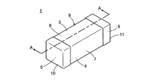
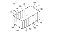
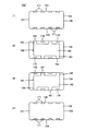
図1ないし図4は、この発明の第1の実施形態を説明するためのものである。ここで、図1は、積層セラミック電子部品1の外観を示す斜視図である。図2は、図1に示した積層セラミック電子部品1の内部構造を示す平面図であり、2つの典型的な断面上での形態を示している。図3は、図1の線A−Aに沿う断面図であり、図4は、図3の一部を拡大して示す断面図である。
1 to 4 are for explaining a first embodiment of the present invention. Here, FIG. 1 is a perspective view showing an appearance of the multilayer ceramic
図1ないし図3に示すように、積層セラミック電子部品1は、複数のセラミック層2が積層されてなり、互いに対向する第1の主面3および第2の主面4と、それらの間を接続する第1ないし第4の側面5〜8とを有するセラミック素体9を備える。第1の側面5および第2の側面6は互いに対向し、第3の側面7および第4の側面8は互いに対向している。
As shown in FIGS. 1 to 3, the multilayer ceramic
第1の側面5上には第1の外部端子電極10が形成され、第2の側面6上には第2の外部端子電極11が形成されている。第1の外部端子電極10および第2の外部端子電極11は、それぞれ、第1および第2の主面3および4ならびに第3および第4の側面7および8の各一部にまで延びるように形成されるが、互いに電気的に絶縁されている。
A first
セラミック素体9の内部には、第1および第2の内部導体12および13が配置されている。各々複数の第1および第2の内部導体12および13を備える場合、第1の内部導体12と第2の内部導体13とは、セラミック層2を介して、積層方向に沿って交互に配置される。第1の内部導体12は、第1の側面5にまで引き出され、第1の外部端子電極10と電気的に接続されている。第2の内部導体13は、第2の側面6にまで引き出され、第2の外部端子電極11と電気的に接続されている。
First and second
図2(1)によく示されているように、第1の内部導体12は、有効部14と、この有効部14から第1の側面5にまで引き出された引出し部15とを有する。図2(2)によく示されているように、第2の内部導体13は、第1の内部導体12の有効部14に対向する有効部16と、この有効部16から第2の側面6にまで引き出された引出し部17とを有する。第1の内部導体12の引出し部15の終端には、第1の側面5上に露出する第1の露出部18が位置し、この第1の露出部18が第1の外部端子電極10との接続部分となっている。他方、第2の内部導体13の引出し部17の終端には、第2の側面6上に露出する第2の露出部19が位置しており、この第2の露出部19が第2の外部端子電極11との接続部分となっている。
As well shown in FIG. 2 (1), the first
第1の内部導体12の有効部14と第2の内部導体13の有効部16とがセラミック層2を挟んで対向する部分において、所定の電気的特性が発現される。
Predetermined electrical characteristics are manifested in a portion where the
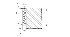
図3に示すように、第1の外部端子電極10は、第1の内部導体12の第2の露出部19を被覆するようにして形成された、金属めっき膜20と、金属めっき膜20を被覆するようにして形成された、Cuめっき膜22とを備える。Cuめっき膜22は、第1の側面5、第1の主面3および第2の主面4と接するように形成され、Cuめっき膜22の内部であって、Cuめっき膜22の少なくともセラミック素体9との界面側に、不連続状にCu酸化物が存在するCu酸化物存在領域21がある。Cu酸化物存在領域21の詳細については、図4を参照して後述する。
As shown in FIG. 3, the first
第2の外部端子電極11も、第1の外部端子電極10と同様、金属めっき膜20、Cu酸化物存在領域21およびCuめっき膜22を備えている。
Similarly to the first
金属めっき膜20は、Cuめっき膜22に含まれるCuと内部導体12および13に含まれる金属との拡散を防止するバリア層として機能し、この拡散によりCuめっき膜22の連続性が低下するのを抑制する。金属めっき膜20の厚みは、3〜7μmであることが好ましい。金属めっき膜20の厚みが3μm未満である場合、金属めっき膜20内部にボイドが形成されることがある。一方、7μmを超える場合、(目標とする厚みにもよるが、)外部端子電極10および11の厚みが厚くなりすぎることがある。金属めっき膜20は、Ni、Sn、Pb、Au、Ag、Pd、BiおよびZnからなる群から選ばれる1種の金属または当該金属を含む合金からなることが好ましい。
The
図4には、図3の一部、すなわち第1の外部端子電極10における、前述したCu酸化物存在領域21が形成されたCuめっき膜22の一部が拡大されて示されている。図示しないが、第2の外部端子電極11側のCuめっき膜22についても同様である。
FIG. 4 is an enlarged view of a part of FIG. 3, that is, a part of the
図4に示すように、第1の外部端子電極10に備えるCuめっき膜22の内部であって、Cuめっき膜22の少なくともセラミック素体9との界面側には、不連続状にCu酸化物21aが存在しているCu酸化物存在領域21が形成されている。図4では、不連続状態の一例として、Cu酸化物21aが玉状に存在している状態が示されているが、必ずしも、このように独立した状態で存在する必要はなく、たとえば、縞状に存在していてもよい。Cu酸化物21aは、セラミック素体9と外部端子電極10とを強固に接合するように作用する。この作用の詳細については後述する。Cu酸化物21aは、Cu2OとCuOとを含み得る。Cu酸化物21aにおいて、Cu2Oの占める割合は90重量%以上であることが好ましい。
As shown in FIG. 4, Cu oxide is discontinuously formed in the
Cuめっき膜22の厚みは、1〜10μmであることが好ましい。Cuめっき膜22を最外層として露出させる場合、Cuめっき膜22の表面には、防錆処理を施してもよい。
The thickness of the
セラミック層2は、たとえば、BaTiO3、CaTiO3、SrTiO3、CaZrO3などを主成分とする誘電体セラミックから構成される。なお、これら主成分に、Mn化合物、Fe化合物、Cr化合物、Co化合物、Ni化合物などの副成分が添加されていてもよい。セラミック層2を構成するセラミックとして、そのほか、PZT系セラミックなどの圧電体セラミック、スピネル系セラミックなどの半導体セラミックなどを用いることもできる。誘電体セラミックを用いた場合は、積層セラミック電子部品1はコンデンサとして機能し、圧電体セラミックを用いた場合は圧電部品として機能し、半導体セラミックを用いた場合はサーミスタとして機能する。また、セラミック層2の厚みは、焼成後において、0.5〜10μmであることが好ましい。
The
内部導体12および13に含まれる導電成分としては、たとえば、Ni、Cu、Ag、PdもしくはAu、またはこれらの金属を含む合金などを用いることができる。なお、金属めっき膜20がNiからなるとき、内部導体12および13には、Niを用いることが特に好ましい。また、内部導体12および13の各々の焼成後の厚みは0.5〜2.0μmであることが好ましい。
As the conductive component contained in the
次に、上述した積層セラミック電子部品1の製造方法の一例について説明する。
Next, an example of a method for manufacturing the above-described multilayer ceramic
まず、セラミック層2となるべきセラミックグリーンシート、内部導体12および13のための導電性ペーストがそれぞれ準備される。これらセラミックグリーンシートおよび導電性ペーストには、バインダおよび溶剤が含まれるが、これらバインダおよび溶剤としては、それぞれ、公知の有機バインダおよび有機溶剤を用いることができる。
First, a conductive green paste for the ceramic green sheet to be the
次に、セラミックグリーンシート上に、たとえばスクリーン印刷法などにより所定のパターンをもって導電性ペーストが印刷される。これによって、内部導体12および13の各々となるべき内部導体パターンが形成されたセラミックグリーンシートが得られる。
Next, a conductive paste is printed on the ceramic green sheet with a predetermined pattern by, for example, a screen printing method. As a result, a ceramic green sheet in which the inner conductor patterns to be the
次に、上述のように内部導体パターンが形成されたセラミックグリーンシートを所定の順序でかつ所定枚数積層し、その上下に導電性ペーストが印刷されていない外層用セラミックグリーンシートを所定枚数積層することによって、生の状態のマザー積層体が得られる。生のマザー積層体は、必要に応じて、静水圧プレスなどの手段により積層方向に圧着される。 Next, a predetermined number of ceramic green sheets having the inner conductor pattern formed thereon are stacked in a predetermined order as described above, and a predetermined number of outer layer ceramic green sheets on which no conductive paste is printed are stacked. Thus, a mother laminate in a raw state can be obtained. The raw mother laminate is pressure-bonded in the laminating direction by means such as an isostatic press as required.
次に、生のマザー積層体は所定のサイズにカットされ、それによって、セラミック素体9の生の状態のものが切り出される。
Next, the raw mother laminate is cut into a predetermined size, whereby the raw
次に、生のセラミック素体9が焼成される。焼成温度は、セラミックグリーンシートに含まれるセラミック材料や導電性ペースト膜に含まれる金属材料にもよるが、たとえば900〜1300℃の範囲に選ばれることが好ましい。
Next, the raw
次に、必要に応じて、バレル研磨等による研磨処理を施し、内部導体12および13の露出部18および19の面出しを行なう。同時に、セラミック素体9の稜部や角部に丸みが形成される。また、必要に応じて、撥水処理を施し、内部導体12および13の露出部18および19とセラミック層2との隙間からのめっき液の浸入を防止しておく。
Next, if necessary, a polishing process such as barrel polishing is performed to expose the exposed
次に、セラミック素体9に第1のめっき処理を施し、第1および第2の内部導体12および13の露出部18および19を被覆するようにして金属めっき膜20を析出させる。
Next, the
次に、第2のめっき処理を施し、上記金属めっき膜20を被覆するように、かつ、金属めっき膜20の周囲に位置するセラミック素体9の第1および第2の側面5および6の各々と接するようにして、Cuめっき膜22を析出させる。このCuめっき膜22は、第3および第4の側面7および8ならびに第1および第2の主面3および4の各一部にまで延びるように析出してもよい。
Next, each of the first and second side surfaces 5 and 6 of the
次に、セラミック素体9に熱処理を施し、上述のCuめっき膜20とセラミック素体9の外表面との間に、Cu液相、O液相およびCu固相を生成させる。これらの混合相は、Cuめっき膜20とセラミック素体9の外表面との界面に偏析しやすい。これは、熱処理時に、Cuめっき膜20とセラミック素体9の外表面との間の微小な隙間やセラミック素体9の表面の微細な空孔に向かって、液相が移動しやすいためであると推測される。
Next, the
熱処理条件は、温度1065℃以上、かつ酸素濃度50ppm以上に選ばれることが好ましい。温度が1065℃未満であったり、酸素濃度が50ppm未満であったりする場合、Cu液相およびO液相が十分生成しないおそれがある。熱処理温度の上限は、Cuの融点を超えない程度とされることが好ましく、具体的には、1084℃未満であることが好ましい。 The heat treatment conditions are preferably selected such that the temperature is 1065 ° C. or higher and the oxygen concentration is 50 ppm or higher. When the temperature is less than 1065 ° C. or the oxygen concentration is less than 50 ppm, the Cu liquid phase and the O liquid phase may not be sufficiently generated. The upper limit of the heat treatment temperature is preferably set so as not to exceed the melting point of Cu, and specifically, it is preferably less than 1084 ° C.
次に、セラミック素体9を室温まで冷却する。このとき、上記界面に偏析したCu液相およびO液相が固体となり、ここに、Cu酸化物21aが形成される。Cu酸化物21aは、セラミック素体9とCuめっき膜22とを強固に接合する。中でも、Cu2Oとセラミックとの間では、拡散接合により、一層強固な接合状態が実現される。また、Cuめっき膜22とセラミック素体9との間がCu酸化物21aにより封止されるため、外部から水分が浸入しにくくなり、積層セラミックコンデンサ1の信頼性を向上させることができる。
Next, the
上述しためっき処理において、めっき方法としては、電解めっきおよび無電解めっきのどちらを採用してもよいが、無電解めっきの場合には、めっき析出速度を向上させるために、触媒などによる前処理が必要となり、工程が複雑化するというデメリットがある。したがって、電解めっきを採用することが好ましい。なお、めっき膜の形成を促進するために、電解めっきまたは無電解めっきの前に、ストライクめっきを施すことが好ましい。また、めっき処理においては、バレルめっきを用いることが好ましい。 In the above-described plating treatment, either electrolytic plating or electroless plating may be employed as the plating method. In the case of electroless plating, in order to improve the plating deposition rate, pretreatment with a catalyst or the like is performed. There is a demerit that the process becomes complicated. Therefore, it is preferable to employ electrolytic plating. In order to promote the formation of the plating film, strike plating is preferably performed before electrolytic plating or electroless plating. In the plating process, it is preferable to use barrel plating.
図5は、この発明の第2の実施形態を説明するための図3に対応する図である。図5において、図3に示す要素に相当する要素には同様の参照符号を付し、重複する説明は省略する。 FIG. 5 is a view corresponding to FIG. 3 for explaining the second embodiment of the present invention. In FIG. 5, elements corresponding to the elements shown in FIG. 3 are denoted by the same reference numerals, and redundant description is omitted.
第2の実施形態による積層セラミック電子部品1aでは、図5に示すように、第1および第2の外部端子電極10および11の各々において、Cuめっき膜22上に上層めっき膜23が形成されている。上層めっき膜23は、たとえば、Cu、Ni、Sn、Pb、Au、Ag、Pd、BiおよびZnからなる群から選ばれる1種の金属または当該金属を含む合金からなることが好ましい。
In the multilayer ceramic
上層めっき膜23は複数層により構成されていてもよい。たとえば、上層めっき膜23の下地となる第1層としては、はんだバリア性能を有するNiを用いることが好ましく、外面を構成する第2層としては、はんだ濡れ性の良いSnやAuを用いることが好ましい。上層めっき膜23の1層あたりの厚みは、1〜15μmであることが好ましい。
The
上層めっき膜23を形成するためのめっき工程は、前述したCu液相、O液相およびCu固相を生成させるための熱処理工程の後に実施されることが好ましい。不連続状にCu酸化物が存在するCu酸化物存在領域21の形成によるめっき液の浸入抑制効果を期待でき、積層セラミック電子部品1aの信頼性を向上させることができるからである。
The plating step for forming the
図6は、この発明の第3の実施形態を説明するための図3に対応する図である。図6において、図3に示した要素に相当する要素には同様の参照符号を付し、重複する説明は省略する。 FIG. 6 is a view corresponding to FIG. 3 for explaining the third embodiment of the present invention. In FIG. 6, elements corresponding to the elements shown in FIG. 3 are denoted by the same reference numerals, and redundant description is omitted.
第3の実施形態による積層セラミック電子部品1bでは、図6に示すように、セラミック素体9の内部において、電気的特性の発現に実質的に寄与しないダミー内部導体24および25が形成される。この実施形態では、ダミー内部導体24および25は、第1または第2の内部電極12または13と同一面上に形成される内層ダミー内部導体24と、第1および第2の内部電極12および13のいずれとも異なる面上に形成される外層ダミー内部導体25とに分類される。
In the multilayer ceramic
ダミー内部導体24および25は、内部電極12および13の場合と同様、セラミック素体2の第1および第2の側面5および6に露出部を有していて、これら露出部も第1または第2の外部端子電極10または11によって被覆され、金属めっき膜20と接続される。これにより、外部端子電極10および11のセラミック素体9に対する固着力をより向上させることができる。なお、ダミー内部導体24および25は、内部導体12および13と同じ金属を含むことが好ましい。
The dummy
図7は、この発明の第4の実施形態を説明するための図3に対応する図である。図7において、図3に示した要素に相当する要素には同様の参照符号を付し、重複する説明は省略する。 FIG. 7 is a view corresponding to FIG. 3 for explaining a fourth embodiment of the present invention. In FIG. 7, elements corresponding to those shown in FIG. 3 are denoted by the same reference numerals, and redundant description is omitted.
第4の実施形態による積層セラミック電子部品1cでは、第1および第2の外部端子電極10および11は、第1の主面3上および第2の主面4上に形成された補助導電層26をさらに備えている。これによって、Cu酸化物存在領域21は、金属めっき膜20と補助導電層26との間に位置するように形成され、Cuめっき膜22は、金属めっき膜20、Cu酸化物存在領域21および補助導電層26を被覆するようにして形成される。
In the monolithic ceramic
補助導電層26が形成されていると、Cuめっき膜22の、第1の主面3上および第2の主面4上でのめっき成長を促進することができ、ひいては、Cu酸化物存在領域21の、第1の主面3上および第2の主面4上での形成をより容易なものとすることができる。
When the auxiliary
補助導電層26は、Ni、Sn、Pb、Au、Ag、Pd、BiおよびZnからなる群から選ばれる1種の金属または当該金属を含む合金からなることが好ましい。また、補助導電層26は、ガラス成分を含み得る。
The auxiliary
補助導電層26は、たとえば、補助導電層26となるべき導体パターン膜が予め形成されたセラミックグリーンシートを、生の状態にあるセラミック素体9の最上層および最下層に積層し、セラミック素体9と同時焼成することにより形成されることができる。あるいは、焼成後のセラミック素体9の第1および第2の主面3および4上に導電性ペーストを印刷して焼き付けることにより形成されてもよい。
The auxiliary
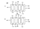
図8および図9は、この発明の第5の実施形態による積層セラミック電子部品101を説明するためのものである。ここで、図8は、積層セラミック電子部品101の外観を示す斜視図である。
8 and 9 are for explaining a multilayer ceramic
積層セラミック電子部品101は、積層セラミックコンデンサアレイを構成するもので、セラミック素体102を備えている。セラミック素体102は、互いに対向する第1および第2の主面103および104と、第1および第2の主面103および104間を結ぶ、第1の側面105、第2の側面106、第3の側面107および第4の側面108とを有する直方体形状をなしている。
The multilayer ceramic
図9は、セラミック素体102の内部構造を示す平面図であり、図9(1)と同(2)とは互いに異なる断面を示している。セラミック素体102は、複数のセラミック層109が積層された構造を有している。セラミック素体102の内部には、互いの間に所定のセラミック層109を介在させた状態で、第1および第2の内部導体110および111が複数組積層方向に交互にかつ主面方向に交互に形成されている。この実施形態では、2つの第1の内部導体110と2つの第2の内部導体111とが主面方向に交互に配列されている。第1の内部導体110は、第1の側面105に露出部112を有し、第2の内部導体111は、第2の側面106に露出部113を有している。
FIG. 9 is a plan view showing the internal structure of the
図8に示すように、セラミック素体102の第1および第2の側面105および106上には、それぞれ、4つの第1の外部端子電極114および4つの第2の外部端子電極115が形成されている。第1の内部導体110の露出部112は、第1の外部端子電極114によって被覆され、第1の外部端子電極114と電気的に接続される。第2の内部導体111の露出部113は、第2の外部端子電極115によって被覆され、第2の外部端子電極115と電気的に接続される。
As shown in FIG. 8, four first external
このような積層セラミック電子部品101の第1および第2の外部端子電極114および115についても、図示しないが、図3または図5を参照して説明した外部端子電極10および11の構造および形成方法が適用される。
The first and second external
第5の実施形態による積層セラミック電子部品101のような多端子型の積層セラミック電子部品においては、外部端子電極の各々の隣り合うもの同士の距離をある程度確保してはんだブリッジを防止する必要があるが、導電性ペーストによる塗布方法の場合、精度良く導電性ペーストを塗布することが困難であるため、露出した内部導体間の距離を少し広めに確保する必要があり、その結果、小型化を阻害している。これに対して、この発明によれば、外部端子電極の形成のために、直接めっきを用いるため、露出した内部導体間の距離を必要最小限に抑えることが可能となり、積層セラミック電子部品の小型化をより進めることができる。
In the multi-terminal multilayer ceramic electronic component such as the multilayer ceramic
なお、第5の実施形態では、8つの端子すなわち内部導体110および111の露出部112および113が合計8つの列を形成していたが、少なくとも4つの列が形成されていればよく、外部端子電極についても、それぞれの列に対応するように少なくとも4つ形成されていればよい。
In the fifth embodiment, the eight terminals, that is, the exposed
図10ないし図12は、この発明の第6の実施形態による積層セラミック電子部品101aを説明するためのものである。ここで、図10および図11は、それぞれ、図8および図9に対応する図である。図12は、外部端子電極114および115を形成する前のセラミック素体102の第1および第2の主面103および104を示す図である。図10ないし図12において、図8および図9に示した要素に相当する要素には同様の参照符号を付し、重複する説明は省略する。
10 to 12 are for explaining a multilayer ceramic
第6の実施形態では、図11に示すように、第1または第2の内部導体110または111と同一面上に形成される内層ダミー内部導体116と、内部導体110および111のいずれとも異なる面上に形成される外層ダミー内部導体117とを備えるとともに、外部端子電極114および115が、図12に示すように、セラミック素体102の第1および第2の主面103および104上に形成される補助導電層118を備えることを特徴としている。
In the sixth embodiment, as shown in FIG. 11, the inner-layer dummy
ダミー内部導体116および117は、第3の実施形態におけるダミー内部導体24および25と同様の作用効果を奏し、補助導電層118は、第4の実施形態における補助導電層26と同様の作用効果を奏する。したがって、第6の実施形態によれば、第5の実施形態に比べて、第1および第2の外部端子電極114および115のセラミック素体102に対する固着力をより向上させることができるとともに、第1および第2の外部端子電極114および115の形成領域を主面103および104にまで容易に延長することができる。
The dummy
なお、第6の実施形態において、ダミー内部導体116および117を省略したり、あるいは、補助導電層118を省略したりすることも可能である。
In the sixth embodiment, the dummy
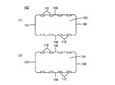
図13および図14は、この発明の第7の実施形態による積層セラミック電子部品151を説明するためのものである。ここで、図13は、積層セラミック電子部品151の外観を示す斜視図である。
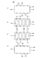
FIGS. 13 and 14 are for explaining a multilayer ceramic
積層セラミック電子部品151は、多端子型低ESL積層セラミックコンデンサを構成するもので、セラミック素体152を備えている。セラミック素体152は、互いに対向する第1および第2の主面153および154と、第1および第2の主面153および154間を結ぶ第1ないし第4の側面155〜158とを有する直方体形状をなしている。
The multilayer ceramic
図14は、セラミック素体152の内部構造を示す平面図であり、図14(1)と同(2)とは互いに異なる断面を示している。
FIG. 14 is a plan view showing the internal structure of the
セラミック素体152は複数のセラミック層159が積層された構造を有している。セラミック素体152の内部には、互いの間に所定のセラミック層159を介在させた状態で、第1および第2の内部導体160および161が複数組積層方向に交互に形成されている。
The
第1の内部導体160は、第2の内部導体161と対向する第1の有効部162と第1の有効部162から第1または第2の側面155または156にまで引き出される複数の第1の引出し部163とを有していて、第1の引出し部163の端部に、第1または第2の側面155または156に露出する露出部164を形成している。
The first
第2の内部導体161は、第1の内部導体160と対向する第2の有効部165と第2の有効部165から第1または第2の側面155または156にまで引き出される複数の第2の引出し部166とを有していて、第2の引出し部166の端部に、第1または第2の側面155または156に露出する露出部167を形成している。
The second
セラミック素体152の第1および第2の側面155および156の各々上には、第1および第2の外部端子電極168および169が交互に複数組配列されている。第1の内部導体160の露出部164は、第1の外部端子電極168によって被覆され、第1の外部端子電極168と電気的に接続される。第2の内部導体161の露出部167は、第2の外部端子電極169によって被覆され、第2の外部端子電極169と電気的に接続される。
A plurality of first and second external
このような第7の実施形態における第1および第2の外部端子電極168および169についても、図3または図5を参照して説明した外部端子電極10および11の構造および形成方法が適用される。
The structure and the formation method of the external
図15ないし図17は、この発明の第8の実施形態による積層セラミック電子部品151aを説明するためのものである。ここで、図15は図13に対応し、図16は図14に対応する図である。図17は、セラミック素体152の第1および第2の主面153および154を示す図である。図15ないし図17において、図13および図14に示した要素に相当する要素には同様の参照符号を付し、重複する説明は省略する。
15 to 17 are for explaining a multilayer ceramic
第8の実施形態の、第7の実施形態に対する関係は、第6の実施形態の、第5の実施形態に対する関係と同様である。すなわち、第8の実施形態では、図16に示すように、第1または第2の内部導体160または161と同一面上に形成される内層ダミー内部導体170と、内部導体160および161のいずれとも異なる面上に形成される外層ダミー内部導体171とを備えるとともに、図17に示すように、セラミック素体152の第1および第2の主面153および154上に形成される補助導電層172を備えることを特徴としている。
The relationship of the eighth embodiment to the seventh embodiment is the same as the relationship of the sixth embodiment to the fifth embodiment. That is, in the eighth embodiment, as shown in FIG. 16, the inner layer dummy
ダミー内部導体170および171は、第3の実施形態におけるダミー内部導体24および25と同様の作用効果を奏し、補助導電層172は、第4の実施形態における補助導電層26と同様の作用効果を奏する。したがって、第8の実施形態によれば、第7の実施形態に比べて、第1および第2の外部端子電極168および169の、セラミック素体152に対する固着力をより向上させることができるとともに、第1および第2の外部端子電極168および169の形成領域を第1および第2の主面153および154にまで容易に延長することができる。
The dummy
なお、第8の実施形態において、ダミー内部導体170および171が省略されても、あるいは、補助導電層172が省略されてもよい。
In the eighth embodiment, the dummy
次に、この発明による効果を確認するために実施した実験例について説明する。この実験例では、第1の実施形態に基づいて積層セラミック電子部品として積層セラミックコンデンサを作製し、評価を行なった。 Next, experimental examples carried out to confirm the effects of the present invention will be described. In this experimental example, a multilayer ceramic capacitor was produced as a multilayer ceramic electronic component based on the first embodiment and evaluated.
まず、以下の表1に示すような仕様を有する積層セラミックコンデンサのためのセラミック素体を準備した。 First, a ceramic body for a multilayer ceramic capacitor having specifications as shown in Table 1 below was prepared.

次に、セラミック素体に外部端子電極を形成するため、以下の表2に示すようなNiめっき浴、Cuめっき浴およびSnめっき浴をそれぞれ用いながら、表3に示すようなめっき条件にて300mlの水平回転バレルを適用することによって、金属めっき膜用Niめっき、Cuめっき膜用Cuめっき、上層めっき膜用Niめっきおよび上層めっき膜用Snめっきをこの順序で実施し、まず、厚み約3μmのNiめっき膜、およびその上に厚み約3μmのCuめっき膜を形成した後、酸素濃度50ppmおよび温度1080℃の条件にて熱処理を施し、さらにその後、厚み約4μmのNiめっき膜、およびその上に厚み約4μmのSnめっき膜を順次形成して、この発明の範囲内の実施例に係る試料とした。 Next, in order to form external terminal electrodes on the ceramic body, 300 ml under the plating conditions as shown in Table 3 while using Ni plating bath, Cu plating bath and Sn plating bath as shown in Table 2 below. By applying this horizontal rotating barrel, Ni plating for metal plating film, Cu plating for Cu plating film, Ni plating for upper layer plating film and Sn plating for upper layer plating film were carried out in this order. After forming a Ni plating film and a Cu plating film with a thickness of about 3 μm thereon, heat treatment was performed under conditions of an oxygen concentration of 50 ppm and a temperature of 1080 ° C., and then a Ni plating film with a thickness of about 4 μm and the top A Sn plating film having a thickness of about 4 μm was sequentially formed to obtain a sample according to an example within the scope of the present invention.
他方、上記金属めっき膜用Niめっきを実施せず、代わりに、Cuめっき膜用Cuめっきを、厚み約8μmのCuめっき膜が形成されるように実施したことを除いて、実施例の場合と同様の工程を経て、この発明の範囲外の比較例に係る試料を作製した。 On the other hand, the Ni plating for the metal plating film was not performed, and instead, the Cu plating for the Cu plating film was performed so that a Cu plating film having a thickness of about 8 μm was formed. A sample according to a comparative example outside the scope of the present invention was manufactured through the same steps.
次に、このようにして得られた実施例および比較例の各々に係る試料について、外部端子電極の固着力を評価するため、外部端子電極を貫通するボイドの発生の有無および1個の試料あたりのボイド発生数を調査した。図18には、試料に係る積層セラミックコンデンサ31の外部端子電極32が形成された部分が拡大されて示されている。積層セラミックコンデンサ31は、セラミック素体33を備え、外部端子電極32は、セラミック素体33の内部においてセラミック層34を挟んで形成された複数の内部導体35と電気的に接続されている。図18には、外部端子電極32を貫通するボイド36が図解的に示されている。
Next, in order to evaluate the fixing force of the external terminal electrode for the samples according to each of the examples and comparative examples obtained in this way, whether or not voids penetrated through the external terminal electrode were generated, and per sample The number of voids was investigated. FIG. 18 shows an enlarged portion of the multilayer
実施例および比較例の各々試料数20個について、図18に示すようなボイドの発生の有無および1個の試料あたりのボイド発生数を調査したところ、実施例では、ボイドの発生は認められなかったのに対し、比較例では、1個の試料あたり平均5.2個のボイドの発生が認められた。 When the number of voids as shown in FIG. 18 and the number of voids generated per sample were investigated for 20 samples in each of the examples and comparative examples, no voids were observed in the examples. On the other hand, in the comparative example, the generation of an average of 5.2 voids per sample was observed.
1,1a,1b,1c,101,101a,151,151a 積層セラミック電子部品
2,109,159 セラミック層
3,4,103,104,153,154 主面
5〜8,105〜108,155〜158 側面
9,102,152 セラミック素体
10,11,114,115,168,169 外部端子電極
12,13,110,111,160,161 内部導体
18,19,112,113,164,167 露出部
20 金属めっき膜
21 Cu酸化物存在領域
22 Cuめっき膜
26,118,172 補助導電層
1, 1a, 1b, 1c, 101, 101a, 151, 151a Multilayer ceramic
Claims (8)
前記セラミック素体の内部に形成され、かつ前記セラミック素体の少なくとも1つの前記側面上に露出部を有する、内部導体と、
前記セラミック素体の少なくとも1つの前記側面上に形成され、かつ前記内部導体の前記露出部を被覆する、外部端子電極と
を備え、
前記外部端子電極は、
前記内部導体の前記露出部を被覆するようにして形成された、金属めっき膜と、
前記金属めっき膜を被覆し、かつ前記セラミック素体と接するようにして形成された、Cuめっき膜と
を備え、
前記Cuめっき膜の内部であって、前記Cuめっき膜の少なくとも前記セラミック素体との界面側に、不連続状にCu酸化物が存在している、
積層セラミック電子部品。 A ceramic comprising a plurality of ceramic layers laminated, and having a first main surface and a second main surface facing each other, and a plurality of side surfaces connecting the first main surface and the second main surface. With the body,
An inner conductor formed inside the ceramic body and having an exposed portion on at least one side of the ceramic body;
An external terminal electrode formed on at least one side surface of the ceramic body and covering the exposed portion of the internal conductor;
The external terminal electrode is
A metal plating film formed so as to cover the exposed portion of the inner conductor;
A Cu plating film formed so as to cover the metal plating film and contact the ceramic body;
Inside the Cu plating film, Cu oxide is present in a discontinuous manner at least on the interface side of the Cu plating film with the ceramic body.
Multilayer ceramic electronic components.
前記Cu酸化物は、前記金属めっき膜と前記補助導電層との間に位置するように形成され、
前記Cuめっき膜は、前記金属めっき膜、前記Cu酸化物および前記補助導電層を被覆するようにして形成される、請求項1または2に記載の積層セラミック電子部品。 The external terminal electrode further includes an auxiliary conductive layer formed on the first main surface and the second main surface,
The Cu oxide is formed so as to be located between the metal plating film and the auxiliary conductive layer,
The multilayer ceramic electronic component according to claim 1, wherein the Cu plating film is formed so as to cover the metal plating film, the Cu oxide, and the auxiliary conductive layer.
前記セラミック素体にめっき処理を施し、前記内部導体の露出部上に金属めっき膜を析出させる工程と、
前記セラミック素体にめっき処理を施し、前記金属めっき膜を被覆するように、かつ、前記金属めっき膜の周囲に位置する前記セラミック素体の前記側面と接するようにして、Cuめっき膜を析出させる工程と、
前記セラミック素体に熱処理を施し、前記Cuめっき膜と前記セラミック素体との間に、Cu液相、O液相およびCu固相を生成させる工程と
を備える、積層セラミック電子部品の製造方法。 A plurality of ceramic layers are laminated, and have a first main surface and a second main surface facing each other, and a plurality of side surfaces connecting between the first main surface and the second main surface, Providing a ceramic body having an inner conductor having an exposed portion on at least one of the side surfaces;
Plating the ceramic body and depositing a metal plating film on the exposed portion of the internal conductor;
The ceramic body is plated, and a Cu plating film is deposited so as to cover the metal plating film and to be in contact with the side surface of the ceramic body located around the metal plating film. Process,
A method of manufacturing a multilayer ceramic electronic component, comprising: heat-treating the ceramic body, and generating a Cu liquid phase, an O liquid phase, and a Cu solid phase between the Cu plating film and the ceramic body.
Priority Applications (2)
| Application Number | Priority Date | Filing Date | Title |
|---|---|---|---|
| JP2009092658A JP5282634B2 (en) | 2008-06-25 | 2009-04-07 | Multilayer ceramic electronic component and manufacturing method thereof |
| US12/490,471 US8125763B2 (en) | 2008-06-25 | 2009-06-24 | Multilayer ceramic electronic component and method for making the same |
Applications Claiming Priority (3)
| Application Number | Priority Date | Filing Date | Title |
|---|---|---|---|
| JP2008165321 | 2008-06-25 | ||
| JP2008165321 | 2008-06-25 | ||
| JP2009092658A JP5282634B2 (en) | 2008-06-25 | 2009-04-07 | Multilayer ceramic electronic component and manufacturing method thereof |
Publications (2)
| Publication Number | Publication Date |
|---|---|
| JP2010034503A true JP2010034503A (en) | 2010-02-12 |
| JP5282634B2 JP5282634B2 (en) | 2013-09-04 |
Family
ID=41447101
Family Applications (1)
| Application Number | Title | Priority Date | Filing Date |
|---|---|---|---|
| JP2009092658A Active JP5282634B2 (en) | 2008-06-25 | 2009-04-07 | Multilayer ceramic electronic component and manufacturing method thereof |
Country Status (2)
| Country | Link |
|---|---|
| US (1) | US8125763B2 (en) |
| JP (1) | JP5282634B2 (en) |
Cited By (10)
| Publication number | Priority date | Publication date | Assignee | Title |
|---|---|---|---|---|
| JP2012009813A (en) * | 2010-05-27 | 2012-01-12 | Murata Mfg Co Ltd | Ceramic electronic component and manufacturing method for the same |
| JP2012064779A (en) * | 2010-09-16 | 2012-03-29 | Murata Mfg Co Ltd | Electronic component |
| JP2013254935A (en) * | 2012-05-08 | 2013-12-19 | Murata Mfg Co Ltd | Electronic component, substrate with built-in electronic component, and method of manufacturing electronic component |
| WO2014057751A1 (en) * | 2012-10-09 | 2014-04-17 | 株式会社村田製作所 | Laminated ceramic electronic component and method for manufacturing same |
| JP2014216638A (en) * | 2013-04-22 | 2014-11-17 | サムソン エレクトロ−メカニックス カンパニーリミテッド. | Multi-layered ceramic capacitor and board for mounting the same |
| US9524828B2 (en) | 2013-04-22 | 2016-12-20 | Samsung Electro-Mechanics, Co., Ltd. | Multilayered ceramic capacitor and mounting the same |
| CN106536130A (en) * | 2015-07-08 | 2017-03-22 | 柳元植 | Brake pad friction material continuous processing apparatus |
| JP2020119965A (en) * | 2019-01-22 | 2020-08-06 | 太陽誘電株式会社 | Multilayer ceramic capacitor and multilayer ceramic capacitor manufacturing method |
| JP2020167376A (en) * | 2019-03-28 | 2020-10-08 | 株式会社村田製作所 | Multilayer ceramic capacitor and manufacturing method of multilayer ceramic capacitor |
| WO2023038032A1 (en) * | 2021-09-08 | 2023-03-16 | 株式会社村田製作所 | Electronic component, and mounting method and mounting structure therefor |
Families Citing this family (41)
| Publication number | Priority date | Publication date | Assignee | Title |
|---|---|---|---|---|
| US8194391B2 (en) * | 2007-12-21 | 2012-06-05 | Murata Manufacturing Co., Ltd. | Multilayer ceramic electronic component and manufacturing method thereof |
| JP5282678B2 (en) * | 2009-06-26 | 2013-09-04 | 株式会社村田製作所 | Multilayer electronic component and manufacturing method thereof |
| JP5382144B2 (en) * | 2010-02-01 | 2014-01-08 | 株式会社村田製作所 | Manufacturing method of electronic parts |
| JP5459487B2 (en) * | 2010-02-05 | 2014-04-02 | 株式会社村田製作所 | Multilayer electronic component and manufacturing method thereof |
| JP5526908B2 (en) * | 2010-03-24 | 2014-06-18 | 株式会社村田製作所 | Multilayer electronic components |
| JP5267583B2 (en) * | 2011-01-21 | 2013-08-21 | 株式会社村田製作所 | Multilayer ceramic electronic components |
| US9490055B2 (en) * | 2011-10-31 | 2016-11-08 | Murata Manufacturing Co., Ltd. | Ceramic electronic component and manufacturing method thereof |
| KR101503967B1 (en) * | 2011-12-08 | 2015-03-19 | 삼성전기주식회사 | Laminated Inductor and Manufacturing Method Thereof |
| KR101983129B1 (en) * | 2012-01-18 | 2019-05-28 | 삼성전기주식회사 | Multi-layered ceramic electronic parts and method of manufacturing the same |
| KR102029468B1 (en) * | 2012-01-18 | 2019-10-07 | 삼성전기주식회사 | Multi-layered ceramic electronic parts and method of manufacturing the same |
| CN104145317B (en) * | 2012-03-05 | 2016-12-21 | 株式会社村田制作所 | Electronic unit |
| DE102012105517B4 (en) * | 2012-06-25 | 2020-06-18 | Tdk Electronics Ag | Multilayer component with an external contact and method for producing a multilayer component with an external contact |
| KR101422926B1 (en) * | 2012-10-26 | 2014-07-23 | 삼성전기주식회사 | Laminated chip electronic component and board for mounting the same |
| KR101452079B1 (en) * | 2012-12-28 | 2014-10-16 | 삼성전기주식회사 | Embedded multilayer capacitor and print circuit board having embedded multilayer capacitor |
| KR101994717B1 (en) * | 2013-07-15 | 2019-07-01 | 삼성전기주식회사 | Multi-layered ceramic capacitor and board for mounting the same |
| KR101525676B1 (en) * | 2013-09-24 | 2015-06-03 | 삼성전기주식회사 | Embedded multilayer ceramic electronic component, manufacturing method thereof and print circuit board having embedded multilayer ceramic electronic component |
| KR101548859B1 (en) * | 2014-02-26 | 2015-08-31 | 삼성전기주식회사 | Multi-layered ceramic electronic parts and board having the same mounted thereon |
| KR102037264B1 (en) * | 2014-12-15 | 2019-10-29 | 삼성전기주식회사 | Device for embedded substrate, method of manufacturing the same and printed circuit board with embedded device |
| KR101652850B1 (en) * | 2015-01-30 | 2016-08-31 | 삼성전기주식회사 | Chip electronic component, manufacturing method thereof and board having the same |
| KR101659208B1 (en) | 2015-02-06 | 2016-09-30 | 삼성전기주식회사 | Multi-Layer Ceramic Electronic Component and Method of Fabricating the Same |
| TWI628678B (en) * | 2016-04-21 | 2018-07-01 | Tdk 股份有限公司 | Electronic component |
| JP6841611B2 (en) * | 2016-07-25 | 2021-03-10 | 太陽誘電株式会社 | Multilayer ceramic capacitors |
| DE102018104459A1 (en) * | 2018-02-27 | 2019-08-29 | Tdk Electronics Ag | Multi-layer component with external contacting |
| JP7089402B2 (en) * | 2018-05-18 | 2022-06-22 | 太陽誘電株式会社 | Multilayer ceramic capacitors and their manufacturing methods |
| JP7145652B2 (en) * | 2018-06-01 | 2022-10-03 | 太陽誘電株式会社 | Multilayer ceramic capacitor and manufacturing method thereof |
| JP7231340B2 (en) | 2018-06-05 | 2023-03-01 | 太陽誘電株式会社 | Ceramic electronic component and manufacturing method thereof |
| JP7446705B2 (en) * | 2018-06-12 | 2024-03-11 | 太陽誘電株式会社 | Multilayer ceramic capacitor and its manufacturing method |
| US11258325B2 (en) | 2018-10-23 | 2022-02-22 | General Electric Company | Articles including insulated conductors and systems thereof |
| CN111755247B (en) * | 2019-03-28 | 2022-01-07 | 株式会社村田制作所 | Multilayer ceramic capacitor and method for manufacturing multilayer ceramic capacitor |
| JP2020202220A (en) * | 2019-06-07 | 2020-12-17 | 株式会社村田製作所 | Multilayer ceramic electronic component |
| KR102333094B1 (en) * | 2019-07-08 | 2021-12-01 | 삼성전기주식회사 | Capacitor component |
| JP7273373B2 (en) * | 2020-04-20 | 2023-05-15 | 株式会社村田製作所 | multilayer ceramic electronic components |
| CN111732455B (en) * | 2020-06-30 | 2022-05-31 | 苏州蓝晶研材料科技有限公司 | Double-tin-layer ceramic conductive material and preparation method thereof |
| JP2022014532A (en) * | 2020-07-07 | 2022-01-20 | 株式会社村田製作所 | Electronic component and manufacturing method for electronic component |
| JP2022014536A (en) * | 2020-07-07 | 2022-01-20 | 株式会社村田製作所 | Electronic component |
| KR20220060286A (en) * | 2020-11-04 | 2022-05-11 | 삼성전기주식회사 | Multilayer capacitor |
| JP2022134972A (en) * | 2021-03-04 | 2022-09-15 | 株式会社村田製作所 | Multilayer ceramic electronic component |
| JP2022136816A (en) * | 2021-03-08 | 2022-09-21 | Tdk株式会社 | Ceramic electronic component |
| KR20230068021A (en) * | 2021-11-10 | 2023-05-17 | 삼성전기주식회사 | Multilayer capacitor |
| KR20230086074A (en) * | 2021-12-08 | 2023-06-15 | 삼성전기주식회사 | Multi-layer capacitor |
| KR20230102525A (en) * | 2021-12-30 | 2023-07-07 | 삼성전기주식회사 | Multilayer electronic component |
Citations (5)
| Publication number | Priority date | Publication date | Assignee | Title |
|---|---|---|---|---|
| JPS5793517A (en) * | 1980-12-02 | 1982-06-10 | Murata Manufacturing Co | Method of forming terminal electrode for chip circuit part |
| JPH02232326A (en) * | 1989-03-07 | 1990-09-14 | Kobe Steel Ltd | Copper material having good joinability with ceramic |
| JP2000100647A (en) * | 1998-09-24 | 2000-04-07 | Kyocera Corp | Laminate ceramic capacitor and manufacture thereof |
| WO2007097180A1 (en) * | 2006-02-27 | 2007-08-30 | Murata Manufacturing Co., Ltd. | Laminated electronic component and method for manufacturing the same |
| JP2008041786A (en) * | 2006-08-03 | 2008-02-21 | Murata Mfg Co Ltd | Laminated ceramic electronic part |
Family Cites Families (17)
| Publication number | Priority date | Publication date | Assignee | Title |
|---|---|---|---|---|
| JP4423707B2 (en) * | 1999-07-22 | 2010-03-03 | Tdk株式会社 | Manufacturing method of multilayer ceramic electronic component |
| TWI260657B (en) * | 2002-04-15 | 2006-08-21 | Avx Corp | Plated terminations |
| US7463474B2 (en) * | 2002-04-15 | 2008-12-09 | Avx Corporation | System and method of plating ball grid array and isolation features for electronic components |
| US6960366B2 (en) * | 2002-04-15 | 2005-11-01 | Avx Corporation | Plated terminations |
| US6982863B2 (en) * | 2002-04-15 | 2006-01-03 | Avx Corporation | Component formation via plating technology |
| US7177137B2 (en) * | 2002-04-15 | 2007-02-13 | Avx Corporation | Plated terminations |
| US7576968B2 (en) * | 2002-04-15 | 2009-08-18 | Avx Corporation | Plated terminations and method of forming using electrolytic plating |
| US7152291B2 (en) * | 2002-04-15 | 2006-12-26 | Avx Corporation | Method for forming plated terminations |
| US7345868B2 (en) * | 2002-10-07 | 2008-03-18 | Presidio Components, Inc. | Multilayer ceramic capacitor with terminal formed by electroless plating |
| GB2400493B (en) | 2003-04-08 | 2005-11-09 | Avx Corp | Plated terminations |
| KR100944099B1 (en) * | 2005-10-28 | 2010-02-24 | 가부시키가이샤 무라타 세이사쿠쇼 | Multilayer electronic component and its manufacturing method |
| WO2007105395A1 (en) * | 2006-03-14 | 2007-09-20 | Murata Manufacturing Co., Ltd. | Method for manufacturing stacked electronic component |
| CN101346786B (en) * | 2006-03-15 | 2011-07-27 | 株式会社村田制作所 | Laminated electronic component and method for manufacturing same |
| JP2009295602A (en) * | 2006-08-22 | 2009-12-17 | Murata Mfg Co Ltd | Laminated electronic component, and method for manufacturing laminated electronic component |
| JP5127703B2 (en) * | 2006-11-15 | 2013-01-23 | 株式会社村田製作所 | Multilayer electronic component and manufacturing method thereof |
| CN101356605B (en) * | 2006-11-22 | 2012-05-23 | 株式会社村田制作所 | Laminated electronic component and method for manufacturing the same |
| JP5289794B2 (en) * | 2007-03-28 | 2013-09-11 | 株式会社村田製作所 | Multilayer electronic component and manufacturing method thereof |
-
2009
- 2009-04-07 JP JP2009092658A patent/JP5282634B2/en active Active
- 2009-06-24 US US12/490,471 patent/US8125763B2/en active Active
Patent Citations (5)
| Publication number | Priority date | Publication date | Assignee | Title |
|---|---|---|---|---|
| JPS5793517A (en) * | 1980-12-02 | 1982-06-10 | Murata Manufacturing Co | Method of forming terminal electrode for chip circuit part |
| JPH02232326A (en) * | 1989-03-07 | 1990-09-14 | Kobe Steel Ltd | Copper material having good joinability with ceramic |
| JP2000100647A (en) * | 1998-09-24 | 2000-04-07 | Kyocera Corp | Laminate ceramic capacitor and manufacture thereof |
| WO2007097180A1 (en) * | 2006-02-27 | 2007-08-30 | Murata Manufacturing Co., Ltd. | Laminated electronic component and method for manufacturing the same |
| JP2008041786A (en) * | 2006-08-03 | 2008-02-21 | Murata Mfg Co Ltd | Laminated ceramic electronic part |
Cited By (17)
| Publication number | Priority date | Publication date | Assignee | Title |
|---|---|---|---|---|
| US8564931B2 (en) | 2010-05-27 | 2013-10-22 | Murata Manufacturing Co., Ltd. | Ceramic electronic component and method for manufacturing the same |
| JP2012009813A (en) * | 2010-05-27 | 2012-01-12 | Murata Mfg Co Ltd | Ceramic electronic component and manufacturing method for the same |
| JP2012064779A (en) * | 2010-09-16 | 2012-03-29 | Murata Mfg Co Ltd | Electronic component |
| US9330848B2 (en) | 2012-05-08 | 2016-05-03 | Murata Manufacturing Co., Ltd. | Electronic component, electronic-component-embedded substrate, and method for producing electronic component |
| JP2013254935A (en) * | 2012-05-08 | 2013-12-19 | Murata Mfg Co Ltd | Electronic component, substrate with built-in electronic component, and method of manufacturing electronic component |
| JPWO2014057751A1 (en) * | 2012-10-09 | 2016-09-05 | 株式会社村田製作所 | Multilayer ceramic electronic component and manufacturing method thereof |
| JP5880725B2 (en) * | 2012-10-09 | 2016-03-09 | 株式会社村田製作所 | Multilayer ceramic electronic component and manufacturing method thereof |
| WO2014057751A1 (en) * | 2012-10-09 | 2014-04-17 | 株式会社村田製作所 | Laminated ceramic electronic component and method for manufacturing same |
| US9620290B2 (en) | 2012-10-09 | 2017-04-11 | Murata Manufacturing Co., Ltd. | Monolithic ceramic electronic component and method for manufacturing the same |
| US9831037B2 (en) | 2012-10-09 | 2017-11-28 | Murata Manufaturing Co., Ltd. | Monolithic ceramic electronic component and method for manufacturing the same |
| JP2014216638A (en) * | 2013-04-22 | 2014-11-17 | サムソン エレクトロ−メカニックス カンパニーリミテッド. | Multi-layered ceramic capacitor and board for mounting the same |
| US9524828B2 (en) | 2013-04-22 | 2016-12-20 | Samsung Electro-Mechanics, Co., Ltd. | Multilayered ceramic capacitor and mounting the same |
| CN106536130A (en) * | 2015-07-08 | 2017-03-22 | 柳元植 | Brake pad friction material continuous processing apparatus |
| JP2020119965A (en) * | 2019-01-22 | 2020-08-06 | 太陽誘電株式会社 | Multilayer ceramic capacitor and multilayer ceramic capacitor manufacturing method |
| JP2020167376A (en) * | 2019-03-28 | 2020-10-08 | 株式会社村田製作所 | Multilayer ceramic capacitor and manufacturing method of multilayer ceramic capacitor |
| JP7215410B2 (en) | 2019-03-28 | 2023-01-31 | 株式会社村田製作所 | Multilayer ceramic capacitor and method for manufacturing the same |
| WO2023038032A1 (en) * | 2021-09-08 | 2023-03-16 | 株式会社村田製作所 | Electronic component, and mounting method and mounting structure therefor |
Also Published As
| Publication number | Publication date |
|---|---|
| US20090323253A1 (en) | 2009-12-31 |
| US8125763B2 (en) | 2012-02-28 |
| JP5282634B2 (en) | 2013-09-04 |
Similar Documents
| Publication | Publication Date | Title |
|---|---|---|
| JP5282634B2 (en) | Multilayer ceramic electronic component and manufacturing method thereof | |
| JP5239731B2 (en) | Multilayer ceramic electronic component and manufacturing method thereof | |
| JP5115349B2 (en) | Multilayer ceramic electronic component and manufacturing method thereof | |
| KR101462754B1 (en) | Multi-layered ceramic electronic parts and fabricating method thereof | |
| US8484815B2 (en) | Method for manufacturing laminated electronic component | |
| US8194391B2 (en) | Multilayer ceramic electronic component and manufacturing method thereof | |
| JP5777179B2 (en) | Multilayer ceramic electronic component for built-in substrate and printed circuit board with built-in multilayer ceramic electronic component | |
| JP2010118499A (en) | Laminated ceramic electronic component | |
| JP2010021524A (en) | Multilayer ceramic electronic component and method of manufacturing same | |
| JP2012156315A (en) | Multilayer ceramic electronic component | |
| JP5694249B2 (en) | Multilayer ceramic electronic components | |
| JP2012164966A (en) | Ceramic electronic component | |
| JP2017228757A (en) | Multilayer ceramic electronic component and mounting board thereof | |
| JP6376604B2 (en) | Multilayer ceramic electronic component for built-in substrate and printed circuit board with built-in multilayer ceramic electronic component | |
| JP2015057810A (en) | Multilayer ceramic electronic component embedded in board and multilayer ceramic electronic component-embedded printed circuit board | |
| JP2017108057A (en) | Multilayer ceramic capacitor | |
| JP2019195037A (en) | Multilayer capacitor | |
| JP2012099786A (en) | Multilayer ceramic capacitor and manufacturing method therefor | |
| US20120147517A1 (en) | Multilayer ceramic capacitor and method of manufacturing the same | |
| JP2013098533A (en) | Manufacturing method for multilayer ceramic electronic component | |
| US20130155573A1 (en) | Electronic component and manufacturing method thereof | |
| JP6309313B2 (en) | Multilayer ceramic electronic component for built-in substrate and printed circuit board with built-in multilayer ceramic electronic component | |
| JP4548471B2 (en) | Capacitor array and manufacturing method thereof | |
| JP2020004942A (en) | Multilayer ceramic capacitor | |
| KR20140013289A (en) | Ceramic electronic component and manufacturing method thereof |
Legal Events
| Date | Code | Title | Description |
|---|---|---|---|
| A621 | Written request for application examination |
Free format text: JAPANESE INTERMEDIATE CODE: A621 Effective date: 20120403 |
|
| A977 | Report on retrieval |
Free format text: JAPANESE INTERMEDIATE CODE: A971007 Effective date: 20130208 |
|
| A131 | Notification of reasons for refusal |
Free format text: JAPANESE INTERMEDIATE CODE: A131 Effective date: 20130219 |
|
| A521 | Request for written amendment filed |
Free format text: JAPANESE INTERMEDIATE CODE: A523 Effective date: 20130411 |
|
| TRDD | Decision of grant or rejection written | ||
| A01 | Written decision to grant a patent or to grant a registration (utility model) |
Free format text: JAPANESE INTERMEDIATE CODE: A01 Effective date: 20130430 |
|
| A61 | First payment of annual fees (during grant procedure) |
Free format text: JAPANESE INTERMEDIATE CODE: A61 Effective date: 20130513 |
|
| R150 | Certificate of patent or registration of utility model |
Ref document number: 5282634 Country of ref document: JP Free format text: JAPANESE INTERMEDIATE CODE: R150 |