JP2010010705A - Nitride semiconductor wafer, method of manufacturing nitride semiconductor device, and nitride semiconductor device - Google Patents
Nitride semiconductor wafer, method of manufacturing nitride semiconductor device, and nitride semiconductor device Download PDFInfo
- Publication number
- JP2010010705A JP2010010705A JP2009233252A JP2009233252A JP2010010705A JP 2010010705 A JP2010010705 A JP 2010010705A JP 2009233252 A JP2009233252 A JP 2009233252A JP 2009233252 A JP2009233252 A JP 2009233252A JP 2010010705 A JP2010010705 A JP 2010010705A
- Authority
- JP
- Japan
- Prior art keywords
- wafer
- work
- affected layer
- grinding
- abrasive grains
- Prior art date
- Legal status (The legal status is an assumption and is not a legal conclusion. Google has not performed a legal analysis and makes no representation as to the accuracy of the status listed.)
- Granted
Links
Images


Abstract
Description
この発明は窒化物半導体ウエハーの外周加工方法に関する。窒化ガリウム(GaN)、窒化アルミニウム(AlN)など3族窒化物半導体はバンドギャップが広く、発光素子や電子デバイスとしての用途がある。大きいGaN単結晶、AlN単結晶は天然に存在しない。異種材料の下地基板の上に原料ガスを流して気相反応で合成する気相成長法、あるいは窒素ガスを金属ナトリウム中に溶解させGaと反応させることで合成するナトリウムフラックス法や超臨界状態のNH3とGaを反応させることで合成するアモノサーマル法と呼ばれる液相法によって作られる。 The present invention relates to a peripheral processing method of a nitride semiconductor wafer. Group III nitride semiconductors such as gallium nitride (GaN) and aluminum nitride (AlN) have a wide band gap and have applications as light emitting elements and electronic devices. Large GaN single crystals and AlN single crystals do not exist in nature. Vapor phase growth method in which raw material gas is flowed on the base substrate of different materials and synthesized by vapor phase reaction, or sodium flux method in which nitrogen gas is dissolved in metallic sodium and reacted with Ga, or supercritical state It is made by a liquid phase method called an ammonothermal method in which NH 3 and Ga are reacted.
初めの頃は自立した窒化ガリウムあるいは窒化アルミニウムなどのウエハーが得られなかったので、サファイヤウエハーの上に、GaN、InGaN、AlGaN薄膜など3族窒化物半導体薄膜をエピタキシャル成長させて発光素子を作っていた。その後GaNの広い自立結晶基板が気相成長法や液相成長法によって製造可能になってきた。現在は、1インチ直径(約25mm)や2インチ直径(約50mm)の自立したGaNウエハー、AlNウエハー、AlGaNウエハー、あるいはInGaNウエハーが作られる。
At the beginning, a self-supporting gallium nitride or aluminum nitride wafer could not be obtained, so a
気相あるいは液相成長させて作った結晶(as−grown)は、表面が平坦でなく厚みもばらついている。これを研削、研磨して表面を平滑にしてミラーウエハーとする。半導体ウエハーはその上に各種のデバイスが作られる基板となるので、表面は平滑でクラックや反りがないということが条件となる。 Crystals (as-grown) produced by vapor phase or liquid phase growth have uneven surfaces and vary in thickness. This is ground and polished to smooth the surface to obtain a mirror wafer. Since the semiconductor wafer becomes a substrate on which various devices are made, the condition is that the surface is smooth and free from cracks and warpage.
ウエハーの外周部が尖っているとそこから欠けたりするのでウエハーの外周部は面取りをする。これをチャンファーという。GaNなどの窒化物半導体結晶は脆くて硬いのでチャンファーには特別の工夫が必要である。 If the outer peripheral portion of the wafer is sharp, it may be chipped from there, so the outer peripheral portion of the wafer is chamfered. This is called chamfer. Since nitride semiconductor crystals such as GaN are brittle and hard, the chamfer requires special measures.
シリコン(Si)ウエハーでもGaAsウエハーでも取扱いに便利なように円形の基板が多く利用される。GaN基板などの窒化物基板でも円形のウエハーが製造される。半導体ウエハーはミラーウエハーにするために表面が研磨される。目的に応じて、両面をミラーにする場合もあるし、片面だけをミラーにする場合もある。 A circular substrate is often used so that it is convenient to handle both a silicon (Si) wafer and a GaAs wafer. Even a nitride substrate such as a GaN substrate produces a circular wafer. The surface of the semiconductor wafer is polished to form a mirror wafer. Depending on the purpose, both sides may be mirrored, or only one side may be mirrored.
面の研磨とは別に、ウエハーの外周部の研削、研磨もある。ウエハーの側周縁が尖っていると欠け易いし細かい屑片ができて表面を傷つけたり汚したりするからである。そこで、ウエハーの側周縁を面取りする。側周縁だけでなくウエハーの側面も研削・研磨することもある。ウエハーの外周部(面の周辺部および側面)を斜めに研削する作業をチャンファー或いはチャンファリングと言う。ベベリングと呼ぶこともあり、これらは同義である。 Apart from surface polishing, there is also grinding and polishing of the outer periphery of the wafer. This is because if the side edge of the wafer is sharp, it tends to be chipped and fine debris is formed, which damages or soils the surface. Therefore, the side edge of the wafer is chamfered. Not only the side edge but also the side surface of the wafer may be ground and polished. The operation of grinding the outer peripheral portion (peripheral portion and side surface of the wafer) obliquely is called chamfering or chamfering. Sometimes called beveling, these are synonymous.
Siウエハーでもチャンファーが成される。しかし、SiウエハーとGaNウエハーなどの窒化物半導体ウエハーは、硬さ、脆さ、堅牢さ等が異なるし化学的な特性も相違する。SiよりもGaNなどの窒化物結晶は硬くて脆い。GaNのGa面などのIII族面を化学的にエッチングすることは困難である。 A chamfer is also formed on a Si wafer. However, nitride semiconductor wafers such as Si wafers and GaN wafers differ in hardness, brittleness, robustness, etc., and in chemical characteristics. A nitride crystal such as GaN is harder and more brittle than Si. It is difficult to chemically etch a group III surface such as a Ga surface of GaN.
Siウエハーで利用されるチャンファー技術を直ちにGaNなどの窒化物半導体ウエハーのチャンファーに転用することはできない。Siウエハーで確立されたチャンファー技術がGaNなどの窒化物半導体ウエハーでも使えるということはない。 The chamfer technology used for Si wafers cannot be immediately transferred to a chamfer for nitride semiconductor wafers such as GaN. The chamfer technology established for Si wafers cannot be used for nitride semiconductor wafers such as GaN.
各々の半導体ウエハーは化学的、機械的な特性が異なるから独自のチャンファー技術が要求される。各々の半導体に最適のチャンファー方法を試行錯誤して、一から探していかなくてはならない。 Since each semiconductor wafer has different chemical and mechanical properties, a unique chamfer technology is required. We have to search for the best chamfer method for each semiconductor by trial and error.
特許文献1は、これまで実在しなかった窒化ガリウムの自立基板をELO(Epitaxial Lateral Overgrowth)によって初めて作ることができたので、外周部を面取りし、オリエンテーションフラット(OF)を付けたというものである。ELOは下地基板として(111)GaAsウエハーを採用する。GaAsウエハーの上に蜂の巣状に分布する細かい窓のあるSiO2マスクを付け、その上にHVPE法でGaN薄膜を横方向成長させ、転位を減らし、マスクの上で結晶粒が合体した後はC面成長させる。
According to
気相成長を続け100μm以上の厚みのGaN結晶にし、GaAs下地基板を除去して、自立GaN基板とする。それは1枚の矩形に近い結晶であるが、円形に研削して円形のウエハーとすることができる。方位と表裏を区別できるために、側周の(1−100)面或いは(2−1−10)面にOF(Orientation Flat)、IF(Identification Flat)を付ける。 Vapor growth is continued to form a GaN crystal having a thickness of 100 μm or more, and the GaAs base substrate is removed to obtain a self-standing GaN substrate. It is a single crystal close to a rectangle, but can be ground into a circular wafer. In order to distinguish between the orientation and the front and back, OF (Orientation Flat) and IF (Identification Flat) are attached to the (1-100) plane or (2-1-10) plane on the side periphery.
特許文献1は側周縁に5゜〜30゜の傾斜角で面取りしたり、半径0.1mm〜0.5mmで円形断面に面取りするということを述べている。前者の場合は円錐台面の砥面を持つ円形砥石を回転させ、GaNウエハーの外周部を円形砥石に(外接)接触させ、外周部を5゜〜30゜の傾斜をなすように削っていくのである。円形砥石は樹脂で固定砥粒を台面に保持したレジンボンド砥石である。
或いは半径0.1mm〜0.5mmの半円断面凹部を持つ糸コマ状の円形の砥石を回転させ、GaNウエハーの外周部を当てて(外接)回転させることによって半円形断面の面取りをすることもできる。 Alternatively, chamfer a semicircular cross section by rotating a thread-shaped circular grindstone having a semicircular cross-sectional recess having a radius of 0.1 mm to 0.5 mm and rotating the outer peripheral portion of the GaN wafer (circumscribed). You can also.
しかしレジンボンド砥石で外周部をチャンファーするとウエハーが割れたり、クラックが発生したりすることが分かった。レジンボンドというのは樹脂によって砥粒を固定した砥石ということである。 However, it was found that when the outer peripheral portion was chamfered with a resin bond grindstone, the wafer was cracked or cracked. The resin bond is a grindstone in which abrasive grains are fixed with resin.
特許文献2では、異種基板の上に窒化ガリウムを成長させ基板を除去して自立したGaNウエハーとしたGaN基板は、下地基板とGaNの熱膨張率や格子定数の違いのために反りが大きい、ということを問題にしている。ウエハーの中心と周辺部の高さの差は±40μm〜±100μmにもなる、と述べている。
In
ウエハーを研磨すると研磨面に加工変質層ができる。研磨によって加工変質層を導入すると加工変質層が面を広げる作用があって、それによって反りを小さくすることができる、と言っている。また加工変質層をエッチングして薄くすると面を押し広げる作用が減るとも言っている。そうすると表面と裏面の研磨とエッチングを組み合わせることによって窒化ガリウムウエハーの反りを減らすことができる、という。 When a wafer is polished, a work-affected layer is formed on the polished surface. It is said that when a work-affected layer is introduced by polishing, the work-affected layer has the effect of expanding the surface, thereby reducing warpage. It is also said that if the work-affected layer is etched and thinned, the effect of expanding the surface is reduced. Then, the warpage of the gallium nitride wafer can be reduced by combining the polishing and etching of the front and back surfaces.
つまり裏面側(窒素面)が凹に反っている場合、裏面側を研磨すると加工変質層が裏面側にできそれが裏面を広げようとする。それによって裏面側が凸になり反りの方向が逆転する。それでは逆に困るので、裏面側をエッチングして加工変質層を除去する。加工変質層が薄くなると裏面を押し広げる力が減るので反りが減る。 That is, when the back surface side (nitrogen surface) warps concavely, when the back surface side is polished, a work-affected layer can be formed on the back surface side, which tends to widen the back surface. As a result, the back side becomes convex and the direction of warping is reversed. Then, since it is troublesome, the back side is etched to remove the work-affected layer. As the work-affected layer becomes thinner, the force that pushes the back surface decreases, so warpage decreases.
ただし、表面側(Ga面)は堅牢であり、研磨が難しい、と述べている。表面側はエッチングも難しいが、表面(Ga面)は塩素プラズマによるドライエッチングが可能である、という。窒化ガリウムウエハーで、研削研磨後に、加工変質層が表面側で10μm厚み、裏面側で50μm厚みで存在することがある。裏面側は、研磨とエッチングの組み合わせによって加工変質層を10μm〜50μmの間の適当な値に調整できるから、反りをかなり少なくすることができる。 However, it states that the surface side (Ga surface) is robust and difficult to polish. Etching is difficult on the surface side, but dry etching with chlorine plasma is possible on the surface (Ga surface). In a gallium nitride wafer, a work-affected layer may exist in a thickness of 10 μm on the front side and 50 μm on the back side after grinding and polishing. On the back surface side, the work-affected layer can be adjusted to an appropriate value between 10 μm and 50 μm by a combination of polishing and etching, so that warpage can be considerably reduced.
特許文献2の実施例1は、表面方向に50μm深さの凹の反りがあるGaNウエハーを表面研削して表面方向に30μmの凸である反りにし、表面をドライエッチングして表面側に20μmの凹である反りのウエハーとし、さらに裏面を研削、ドライエッチングして表面側に5μmの凹である少ない反りのウエハーとしている。特許文献2は研削、エッチングの組み合わせによって最終的に2インチウエハー換算で反りを+30μm〜−20μmに減少させることができると主張している。
In Example 1 of
正は表面が凸になる反り、負は表面が凹になる反りだとして定義されている。よって特許文献2はGaNウエハーにおいて、表面凸反りが30μmから、表面凹反りが20μmという凹凸反りの範囲に入れることができると述べているのである。
Positive is defined as warping with a convex surface and negative is warping with a concave surface. Therefore,
特許文献3は、レジンボンドダイヤモンド砥石をGaNウエハーのエッジに外接回転させてGaNウエハーのチャンファーを行うと、GaNは脆く硬い材料であるからエッジが欠けたりウエハーが割れたりするので望ましくないと述べている。
特許文献3はそこで、砥石を付着させたテープ砥石をウエハーのエッジの長手方向に接触させウエハーを回転させることによってウエハーの面取りをするというテープ砥石チャンファリング法を提案している。砥石が摩耗するとテープを少しずつ送り新しい砥面を出してエッジ研磨を同じ状態で行うようにできる。エッジはテープに内接するから接触圧が小さく衝撃も掛からない。レジンボンド砥石を外接回転させる手法に比べて歩留まりが向上すると説明している。
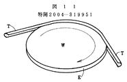
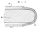
本願の図11は特許文献3(特開2004−319951号)によって初めて提案されたテープチャンファー装置の斜視図である。本願の図12はテープ砥石とエッジの接触部分の断面図である。 FIG. 11 of the present application is a perspective view of a tape chamfer device proposed for the first time by Japanese Patent Application Laid-Open No. 2004-319951. FIG. 12 of the present application is a sectional view of a contact portion between the tape grindstone and the edge.
ウエハーWは回転盤(図示しない)に真空チャック等で固定してある。テープ砥石TにエッジSが内接している。内接部分の中心角は40゜〜90゜であるとしている。弾力性のあるテープとの接触であるからエッジが破損したり割れたりすることを防ぐことができると述べている。 The wafer W is fixed to a rotating disk (not shown) with a vacuum chuck or the like. An edge S is inscribed in the tape grindstone T. The central angle of the inscribed portion is 40 ° to 90 °. It states that the edge can be prevented from being broken or cracked because of the contact with the elastic tape.
窒化ガリウムなどの窒化物半導体自立結晶が気相成長法や液相成長法で製造できるようになった。液相成長法では大型結晶を得るのは困難である。気相成長法によって広い下地基板の上に窒化ガリウムを厚く堆積させ窒化ガリウムの部分をワイヤーソーで切断し窒化ガリウムの大型自立結晶基板を作製することができる。これを裏面研削、チャンファー、表面研削・研磨して窒化物半導体ミラーウエハーとする。 Nitride semiconductor free-standing crystals such as gallium nitride can be manufactured by vapor phase growth or liquid phase growth. It is difficult to obtain large crystals by the liquid phase growth method. A large-sized self-supporting crystal substrate of gallium nitride can be manufactured by depositing gallium nitride thickly on a wide base substrate by a vapor deposition method and cutting the gallium nitride portion with a wire saw. This is subjected to backside grinding, chamfering, surface grinding / polishing to obtain a nitride semiconductor mirror wafer.
研削によって厚い(10μm〜50μm)加工変質層が接触部分に発生する。裏面研削では裏面に、外周研削では外周部に、表面研削では表面に加工変質層ができる。加工変質層は結晶構造の乱れを持つ表面層である。転位も多量に含む。不純物を含むものではない。加工変質層が表面、裏面に残ってはいけないので表面、裏面の加工変質層はエッチングによって殆ど除去される。この発明は外周部の研削(チャンファー)を問題にする。SiやGaAsなど従来の半導体ウエハーのチャンファーにはダイヤモンド砥粒を樹脂や金属で基盤に固定したレジンボンド砥石やメタルボンド砥石が使われてきた。これらは鋭利で硬く堅牢でチャンファー時間は短くて済む。Si、GaAsウエハーは柔らかく靭性もあるのでレジンボンド、メタルボンド砥石が適するのである。しかしこれらはGaNチャンファーに転用できない。レジンボンド砥石やメタルボンド砥石によってGaNウエハーをチャンファーすると、割れ欠けの(クラック)発生率が高く、厚い加工変質層を生じ、大きい反りを引き起こすことが分かってきた。GaNは硬度が高く靭性が低く脆いから衝撃に弱い。クラック発生率が高いのは、レジンボンド、メタルボンド砥石は基盤に対する砥粒の固定が硬直しており砥粒とウエハーの接触衝撃を吸収できないからである。レジンボンド、メタルボンド砥石によるチャンファーによって割れ欠けが頻繁に起こり、そうでなかったとしても外周部に20μm〜50μmもの厚い加工変質層Mができる。また反りも大きくなる。反りの曲率半径は1m以下ということもある。高硬度高脆性のGaNウエハーのチャンファーには従来のレジンボンド、メタルボンド砥石は不適である。 A thick (10 μm to 50 μm) work-affected layer is generated at the contact portion by grinding. In the back grinding, a work-affected layer is formed on the back surface, in the outer periphery grinding on the outer periphery, and in the surface grinding on the surface. The work-affected layer is a surface layer having a disordered crystal structure. It contains a large amount of dislocations. Does not contain impurities. Since the work-affected layer should not remain on the front and back surfaces, the work-affected layers on the front and back surfaces are almost removed by etching. In the present invention, grinding of the outer peripheral portion (chamber) is a problem. For semiconductor wafer chamfers such as Si and GaAs, resin bond grindstones and metal bond grindstones in which diamond abrasive grains are fixed to the base with resin or metal have been used. They are sharp, hard and robust and require less chamfer time. Since Si and GaAs wafers are soft and tough, resin bond and metal bond grindstones are suitable. However, these cannot be diverted to GaN chamfers. It has been found that when a GaN wafer is chamfered with a resin bond grindstone or a metal bond grindstone, the crack generation rate is high, a thick work-affected layer is formed, and a large warp is caused. Since GaN has high hardness, low toughness and is brittle, it is vulnerable to impact. The reason why the crack generation rate is high is that resin-bonded and metal-bonded grindstones are hard to fix the abrasive grains to the substrate and cannot absorb the contact impact between the abrasive grains and the wafer. Cracks are frequently generated by chamfering with a resin bond or a metal bond grindstone, and even if this is not the case, a thick work-affected layer M of 20 μm to 50 μm can be formed on the outer periphery. Also, the warpage is increased. The curvature radius of warpage may be 1 m or less. Conventional resin bond and metal bond grindstones are not suitable for chamfers of GaN wafers with high hardness and brittleness.
窒化物半導体ウエハーを割れ欠けしないように外周研削する加工方法を提供することが本発明の第1の目的である。反りの少ない窒化物半導体ウエハーを得るための外周研削加工方法を提供することが本発明の第2の目的である。外周部の加工変質層厚みを制御した窒化物半導体の外周研削加工方法を提供することが本発明の第3の目的である。基板作製プロセス歩留まりの高い窒化物半導体の外周研削加工方法を提供することが本発明の第4の目的である。デバイス面内歩留まりの高い外周研削加工方法を提供することが本発明の第5の目的である。また、デバイス面内歩留まりの高い窒化物半導体ウエハーを得る事が本発明の第6の目的である。なお本出願では、ウエハーの表面、裏面の平面の外側の領域を周辺部とし、平面と側面の角を側周縁とし、平面の周辺部と側面を含めて外周部とする。 It is a first object of the present invention to provide a processing method for grinding an outer periphery of a nitride semiconductor wafer so as not to crack and chip. It is a second object of the present invention to provide a peripheral grinding method for obtaining a nitride semiconductor wafer with less warpage. It is a third object of the present invention to provide a nitride semiconductor peripheral grinding method in which the thickness of the work-affected layer in the peripheral portion is controlled. It is a fourth object of the present invention to provide a method for peripheral grinding of a nitride semiconductor with a high substrate manufacturing process yield. It is a fifth object of the present invention to provide a peripheral grinding method with a high device surface yield. It is a sixth object of the present invention to obtain a nitride semiconductor wafer having a high device in-plane yield. In the present application, a region outside the plane of the front and back surfaces of the wafer is defined as a peripheral portion, a corner between the plane and the side is defined as a peripheral edge, and a peripheral portion including the peripheral portion and the side surface of the plane is defined as a peripheral portion.
本発明の窒化物半導体ウエハーは、アズグロウンの基板の裏面を研削、エッチングし、ダイヤモンドあるいはダイヤモンドと酸化物の混合砥粒を柔軟なボンディング材で固定した砥石によって外周研削(チャンファー)して、ウエハー外周部の加工変質層の厚みを0.5μm〜10μm、特に望ましくは1μm〜3μmとし、表面を研削、研磨、エッチングしたものである。柔軟なボンディング材というのはゴム、或いは発泡樹脂である。ダイヤモンド砥粒の粒径はある程度細かくて3000番手から600番手である。またダイヤモンド砥粒に酸化物砥粒を混合して酸化物の化学的作用とダイヤモンドの機械的作用の複合作用で研削する。ダイヤモンド砥粒の機械的効果に加えて酸化物の化学的効果で表面を除去するのでこれをメカノケミカル効果という。酸化物砥粒はFe2O3、CuO、MnO2、Cr2O3、ZnOなどである。柔軟性に富む砥石でチャンファーするので時間が長く掛かる場合もある。 The nitride semiconductor wafer of the present invention is obtained by grinding and etching the back surface of an as-grown substrate, and grinding the outer periphery with a grindstone in which diamond or a mixed abrasive of diamond and oxide is fixed with a flexible bonding material. The thickness of the work-affected layer at the outer peripheral portion is 0.5 μm to 10 μm, particularly preferably 1 μm to 3 μm, and the surface is ground, polished, and etched. The flexible bonding material is rubber or foamed resin. The diameter of the diamond abrasive grains is fine to some extent and is from 3000 to 600. Also, diamond abrasive grains are mixed with oxide abrasive grains and ground by the combined action of oxide chemical action and diamond mechanical action. Since the surface is removed by the chemical effect of oxides in addition to the mechanical effect of diamond abrasive grains, this is called the mechanochemical effect. The oxide abrasive grains are Fe 2 O 3 , CuO, MnO 2 , Cr 2 O 3 , ZnO and the like. Chamfering with a flexible grinding wheel may take a long time.
細かいダイヤモンド砥粒と酸化物砥粒を柔軟な材料で基盤に付けた砥石でチャンファーすることによって、ウエハー外周へかかる衝撃を和らげ、割れ欠け(クラック)の発生を防ぎ、加工変質層の厚みを低減し、反りを抑える。外周部への機械衝撃を緩和するためにゴムボンド、発泡樹脂ボンド砥石を利用する。外周部に発生する加工変質層Mの厚みdは、外周部が受けた衝撃を測定する尺度にもなる。ダイヤモンド砥粒が粗くボンド材が硬直していると衝撃力が大きい。そのとき外周部を後で観察すると加工変質層厚みdが厚くなっている。ダイヤモンド砥粒が細かくボンド材が柔軟であると衝撃力が小さい。そのとき外周部を後で観察すると加工変質層厚みdが薄くなっている。 By chamfering with a grindstone with fine diamond abrasive grains and oxide abrasive grains attached to the base with a flexible material, the impact applied to the outer periphery of the wafer is reduced, cracking is prevented, and the thickness of the work-affected layer is reduced. Reduce and suppress warping. A rubber bond or a foamed resin bond grindstone is used to alleviate the mechanical impact on the outer periphery. The thickness d of the work-affected layer M generated at the outer peripheral portion also serves as a scale for measuring the impact received by the outer peripheral portion. When the diamond abrasive grains are rough and the bond material is hard, the impact force is large. At that time, when the outer peripheral portion is observed later, the work-affected layer thickness d is increased. If the diamond abrasive grains are fine and the bond material is flexible, the impact force is small. At that time, when the outer peripheral portion is observed later, the thickness d of the work-affected layer is reduced.
低番手砥粒を樹脂、金属で基盤に固定したレジンボンド、メタルボンドなど硬質の砥石で外周部を削ると加工変質層厚みdが20μm〜50μmにもなる。この場合は衝撃が強すぎ割れ欠けが起こる。本発明がd=0.5μm〜10μmになるように柔軟な砥石で優しくチャンファーすることによって、割れ欠け、反りを抑制している。柔軟な砥石にするためゴム、発泡樹脂をボンド剤とし、粒径の小さい高番手のダイヤモンド砥粒を使い、酸化物を混ぜるようにする。割れ欠け、反りの少ないGaNウエハーのチャンファーが可能となる。適当な優柔性の砥石でチャンファーすると、外周部加工変質層厚みdが0.5μm〜10μmになる。この厚みの加工変質層により反りを抑制し、デバイスの歩留まりを向上することができる。 When the outer peripheral portion is shaved with a hard grindstone such as a resin bond or a metal bond in which low count abrasive grains are fixed to the substrate with resin or metal, the work-affected layer thickness d becomes 20 μm to 50 μm. In this case, the impact is too strong and cracks occur. By chamfering gently with a flexible grindstone so that d = 0.5 μm to 10 μm, the present invention suppresses cracking and warping. In order to make a flexible grinding wheel, rubber and foamed resin are used as a bonding agent, and high-diamond diamond grains with a small particle size are used to mix oxides. It is possible to chamfer a GaN wafer with less cracking and warping. When chamfering with a suitable gentle grindstone, the outer peripheral part processed damaged layer thickness d becomes 0.5 μm to 10 μm. Warpage can be suppressed by the work-affected layer having this thickness, and the device yield can be improved.
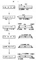
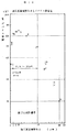
窒化ガリウム自立結晶(アズグロウンウエハー)から出発する加工の工程全般を説明する。図1の順にウエハーを加工する。厚み調整のため裏面(窒素面)研削(A)をする。これによって裏面に厚い加工変質層Mが発生する。加工変質層Mというのは結晶構造が歪んだ層をいう。多数の転位が存在する。加工変質層はCL(カソードルミンネセンス)によって他の部分と区別して観察できる。CL観察で厚みdを測ることもできる。加工変質層は不純物を含む層ではない。加工変質層が裏面に厚く残るのは望ましくない。加熱したKOH、NaOH、H3PO4水溶液で裏面(窒素面)をエッチング(B)する。これによって裏面の加工変質層を除去する。なお、裏面研削は研磨で代替することもできる。 An overall processing process starting from a gallium nitride free-standing crystal (as-grown wafer) will be described. The wafers are processed in the order shown in FIG. The back surface (nitrogen surface) is ground (A) for thickness adjustment. As a result, a thick work-affected layer M is generated on the back surface. The work-affected layer M is a layer in which the crystal structure is distorted. There are many dislocations. The work-affected layer can be observed separately from other parts by CL (cathodoluminescens). The thickness d can also be measured by CL observation. The work-affected layer is not a layer containing impurities. It is not desirable that the work-affected layer remains thick on the back surface. The back surface (nitrogen surface) is etched (B) with heated KOH, NaOH, H 3 PO 4 aqueous solution. As a result, the work-affected layer on the back surface is removed. Note that the back surface grinding can be replaced by polishing.
高番手のダイヤモンド砥粒、或いはダイヤモンド砥粒と酸化物をゴム又は発泡樹脂でボンドした柔軟性ある砥石で窒化ガリウムウエハーの外周部を研削する(C)。ウエハー外周部の研削をチャンファー加工と呼ぶ。チャンファーするのはウエハーの割れ、欠けを防ぐためである。
GaNウエハーのチャンファーに使用する砥石はゴム砥石が好ましいと本発明者は考える。ゴム砥石というのは、砥石基盤にゴムをボンディング剤として砥粒を固定したものである。砥粒はダイヤモンドなど硬質の素材である。ゴムをボンディング剤とするので、ゴムボンディング砥石或いはゴムボンド砥石というべきであるが、ここでは簡単にゴム砥石と呼ぶ。砥粒がゴムだということではない。GaNウエハーの外周研削にゴム砥石を使用するのは本発明が初めてである。
The outer peripheral portion of the gallium nitride wafer is ground with a high-quality diamond abrasive or a flexible grindstone in which diamond abrasive and oxide are bonded with rubber or foamed resin (C). Grinding the wafer outer periphery is called chamfering. The reason for chamfering is to prevent cracking and chipping of the wafer.
The present inventor believes that the grindstone used for the chamfer of the GaN wafer is preferably a rubber grindstone. A rubber grindstone is one in which abrasive grains are fixed to a grindstone base using rubber as a bonding agent. The abrasive is a hard material such as diamond. Since rubber is used as a bonding agent, it should be called a rubber bonding grindstone or a rubber bond grindstone, but here it is simply called a rubber grindstone. It does not mean that the abrasive is rubber. The present invention is the first to use a rubber grindstone for peripheral grinding of a GaN wafer.
チャンファーの後、ウエハーの表面を研削(D)、研磨(E)する。研削では表面に10μm〜50μmの厚い加工変質層Mができる。研磨では表面に0.1μm〜20μmの加工変質層ができる。エピタキシャル成長用の基板としては、表面粗さが平滑で、表面に加工変質層Mが存在しないものが望まれる。そのため研削後に研磨工程で表面を平滑化する。更に、気相エッチング(F)によって表面の加工変質層Mがなくなるまで除去する。ウエハー加工はそのように裏面研削A、裏面エッチングB、チャンファーC、表面研削D・研磨E、気相エッチング(F)の工程からなる。本発明の工夫は裏面研削A、表面研削D・研磨Eにはない。本発明はチャンファー工程Cを改良するものである。 After the chamfering, the surface of the wafer is ground (D) and polished (E). In grinding, a thick work-affected layer M of 10 μm to 50 μm is formed on the surface. By polishing, a work-affected layer of 0.1 to 20 μm is formed on the surface. As a substrate for epitaxial growth, a substrate having a smooth surface roughness and having no work-affected layer M on the surface is desired. Therefore, the surface is smoothed by a polishing process after grinding. Further, it is removed by vapor phase etching (F) until there is no work-affected layer M on the surface. Wafer processing is thus composed of the steps of back grinding A, back etching B, chamfer C, surface grinding D / polishing E, and vapor phase etching (F). The invention of the present invention does not exist in back grinding A, surface grinding D / polishing E. The present invention improves the chamfer process C.
本発明の骨子は、窒化物半導体ウエハー外周部を、高番手ダイヤモンド砥粒あるいはダイヤモンド砥粒と酸化物砥粒をゴム、発泡樹脂で固定したゴム砥石あるいは発泡レジンボンド砥石でチャンファー加工し、外周部の加工変質層厚みを0.5μm〜10μm、特に望ましくは1μm〜3μmにしたことにある。外周部の加工変質層を0.5μm〜10μmに抑えることによって、クラック発生、反りが少なくなる。後の工程におけるチッピングも減り、製品歩留まりも上がる。 The gist of the present invention is that the outer periphery of a nitride semiconductor wafer is chamfered with a high-quality diamond abrasive grain or a diamond grinder and an oxide abrasive grain fixed with rubber, foamed resin or a foamed resin bond grindstone. The thickness of the work-affected layer is 0.5 μm to 10 μm, particularly preferably 1 μm to 3 μm. By suppressing the work-affected layer at the outer peripheral portion to 0.5 μm to 10 μm, crack generation and warpage are reduced. Chipping in later processes is reduced and product yield is increased.
以下により詳しく述べる。研削によって結晶表面には格子構造の乱れた加工変質層Mが必ず発生する。加工変質層Mの厚みdは、研削に使われる固定砥粒の粒子が大きい程厚くなり、又加工負荷が強い程厚くなる。その反対に研削に使われる固定砥粒が小さく、加工負荷が弱い程、加工変質層Mは薄くなる。 More detailed below. Grinding always causes a work-affected layer M having a disordered lattice structure on the crystal surface. The thickness d of the work-affected layer M becomes thicker as the fixed abrasive grains used for grinding become larger, and becomes thicker as the work load becomes stronger. Conversely, the smaller the fixed abrasive used for grinding and the weaker the processing load, the thinner the work-affected layer M becomes.
ウエハーの加工は、図1に示すように、裏面研削A、裏面エッチングB、外周研削(チャンファー)C、表面研削D、研磨E、表面エッチングFの順で行う。研削条件にもよるが裏面研削Aによって、10μm〜50μm程度のかなり厚い加工変質層Mが裏面に発生する。加工変質層が厚く残留するのは望ましくない。裏面の加工変質層を加熱したKOH、NaOH、又はH3PO4水溶液で除去する。 As shown in FIG. 1, the wafer is processed in the order of back surface grinding A, back surface etching B, peripheral grinding (chamber) C, surface grinding D, polishing E, and surface etching F. Although depending on the grinding conditions, a considerably thick work-affected layer M of about 10 μm to 50 μm is generated on the back surface by back surface grinding A. It is undesirable for the work-affected layer to remain thick. The work-affected layer on the back surface is removed with heated KOH, NaOH, or H 3 PO 4 aqueous solution.
N面とGa面は化学的、物理的な性質が異なる。裏面(窒素面;N面;000−1面)は表面より物理的化学的に弱くてKOH、NaOH、又はH3PO4水溶液で除去できる。裏面をエッチングできるものであれば、他のアルカリ、酸を用いても良い。表面(Ga面;0001面)は化学的により堅固でKOH、NaOH、又はH3PO4水溶液では除去できない。従って裏面と表面では加工変質層除去の手段が異なる。 The N face and Ga face are different in chemical and physical properties. The back surface (nitrogen surface; N surface; 000-1 surface) is physically and chemically weaker than the surface, and can be removed with an aqueous solution of KOH, NaOH, or H 3 PO 4 . Other alkalis and acids may be used as long as the back surface can be etched. The surface (Ga face; 0001 face) is chemically harder and cannot be removed with an aqueous solution of KOH, NaOH, or H 3 PO 4 . Accordingly, the means for removing the work-affected layer differs between the back surface and the front surface.
次いでウエハーの外周部をチャンファーする。砥粒をゴムで固めたゴム(ボンド)砥石あるいは発泡樹脂で砥粒を固めた発泡レジンボンド砥石を回転させ、ウエハー外周部に接触させ外周部を面取りする。固定砥粒はダイヤモンド砥粒、或いはダイヤモンドと酸化物の混合砥粒である。ゴムボンド砥石、発泡レジンボンド砥石が含むダイヤモンド砥粒の番手は例えば600番〜3000番とする。番手というのは砥粒の平均の直径の大きさを表す用語である。数字が大きいほど細かい砥粒を意味する。チャンファーによってウエハーの外周部が面取りされるが、同時に外周部に加工変質層が発生する。加工変質層の厚みdを0.5μm〜10μmとする。より好ましくはd=1μm〜3μmとする。ダイヤモンド砥粒の粒径が大きい(番手が小さい)砥石でチャンファーするとdが20μm〜50μmになり、反りが大きくしばしば研削中に割れ欠けが生ずる(クラック)。砥粒の粒径を小さくするとdを減らすことができるがそれだけでは不十分である。酸化物砥粒を加えてダイヤモンドの機械作用を緩和するのも有効である。酸化物にはFe2O3、Cr2O3、MnO2、CuO、ZnO、Fe3O4などの化学的に不安定な酸化物を用いることができる。本発明者が初めて金属酸化物で、ある種の砥粒が化学作用を持ち、それが窒化物の研削を促進する効果を有することを発見した。これを本発明者はメカノケミカル研削(mechanochemical grinding)と名付けた。
メカノケミカル研削は、酸化物砥粒による酸化等の反応により窒化物の表面を軟質化し、研削の負荷を低減する方法であり、研削加工時の加工変質層やクラックを抑制できる。
Next, the outer periphery of the wafer is chamfered. A rubber (bond) grindstone in which abrasive grains are hardened with rubber or a foamed resin bond grindstone in which abrasive grains are hardened with foamed resin is rotated and brought into contact with the outer peripheral portion of the wafer to chamfer the outer peripheral portion. The fixed abrasive is diamond abrasive or a mixed abrasive of diamond and oxide. The diamond abrasive grains included in the rubber bond grindstone and the foamed resin bond grindstone are, for example, 600-3000. The count is a term representing the average diameter of the abrasive grains. A larger number means finer abrasive grains. Although the outer periphery of the wafer is chamfered by the chamfer, a work-affected layer is generated on the outer periphery at the same time. The thickness d of the work-affected layer is set to 0.5 μm to 10 μm. More preferably, d = 1 μm to 3 μm. When chamfering with a grindstone having a large diamond abrasive grain size (small count), d becomes 20 μm to 50 μm, and warping is large, and cracks are often generated during grinding (cracks). If the grain size of the abrasive grains is reduced, d can be reduced, but that alone is not sufficient. It is also effective to reduce the mechanical action of diamond by adding oxide abrasive grains. As the oxide, a chemically unstable oxide such as Fe 2 O 3 , Cr 2 O 3 , MnO 2 , CuO, ZnO, or Fe 3 O 4 can be used. The inventor has discovered for the first time that metal oxides, certain abrasive grains have a chemical action, which has the effect of promoting nitride grinding. The inventor named this as mechanochemical grinding.
Mechanochemical grinding is a method of softening the surface of a nitride by a reaction such as oxidation by oxide abrasive grains to reduce the grinding load, and can suppress a work-affected layer and cracks during grinding.
酸化物といってもSiO2、Al2O3のような安定な酸化物は不適でこれらはメカノケミカル研削の作用がない。安定な酸化物を加えてもdを10μm以下にするにはなかなか至らない。砥石基盤に砥粒を固定するボンディング材は柔軟性をもつゴムあるいは発泡樹脂にする。ダイヤモンド砥粒の番手を高く、酸化物砥粒を加え、ボンド材を柔軟にする、という3つの条件を相補的に組み合わせることでdを10μm以下にすることができる。本発明は窒化物半導体ウエハーのチャンファーに初めてゴムボンド砥石、発泡樹脂ボンド砥石の使用を提案する。本発明は窒化物半導体ウエハーのチャンファーに初めて酸化物砥粒混合砥石を提案する。
この後更に表面を研削する。表面に加工変質層が入る。表面はデバイスをその上に作る面であるからミラー状態でなければならない。そのため表面を研磨する。研磨には粗い砥粒を使う粗研磨と、細かい砥粒を使う仕上げ研磨を行うことができる。例えば粗研磨には粒径30μm〜3μmの砥粒を用いることができ、仕上げ研磨には3μm〜0.1μmの砥粒を用いることができる。研磨によってウエハーの表面に加工変質層が入る。なお、平面加工である研削、研磨は生産性と表面品質の両立のために表面について段階的に実施することが多いが、どちらかを省略することもできる。この場合、研削には番手が3000番〜8000番の砥石を用い、研磨には30μm〜15μmの砥粒を用いることができる。研削で高番手の砥石を用いる事により研磨を省略することや、研磨で粗い砥粒を用いることにより研削を省略することもできる。この場合、研削には番手が3000番〜8000番の砥石を用い、研磨には30μm〜15μmの砥粒を用いることができる。
Stable oxides such as SiO 2 and Al 2 O 3 are unsuitable even though they are oxides, and these have no mechanochemical grinding action. Even when a stable oxide is added, it is difficult to reduce d to 10 μm or less. The bonding material for fixing the abrasive grains to the wheel base is made of flexible rubber or foamed resin. The d can be reduced to 10 μm or less by complementarily combining the three conditions of increasing the diamond abrasive count, adding oxide abrasive grains, and softening the bond material. The present invention proposes the use of a rubber bond grindstone and a foamed resin bond grindstone for the first time for a chamfer of a nitride semiconductor wafer. The present invention proposes for the first time an oxide abrasive mixed grindstone for a chamfer of a nitride semiconductor wafer.
After this, the surface is further ground. A work-affected layer enters the surface. Since the surface is the surface on which the device is made, it must be mirrored. Therefore, the surface is polished. For polishing, rough polishing using coarse abrasive grains and finish polishing using fine abrasive grains can be performed. For example, abrasive grains having a particle size of 30 μm to 3 μm can be used for rough polishing, and abrasive grains of 3 μm to 0.1 μm can be used for finish polishing. A work-affected layer enters the surface of the wafer by polishing. In addition, although grinding and polishing, which are planar processes, are often performed stepwise on the surface in order to achieve both productivity and surface quality, either one can be omitted. In this case, a grindstone having a count of 3000 to 8000 can be used for grinding, and abrasive grains of 30 μm to 15 μm can be used for polishing. Polishing can be omitted by using a high-quality grindstone in grinding, or grinding can be omitted by using coarse abrasive grains in polishing. In this case, a grindstone having a count of 3000 to 8000 can be used for grinding, and abrasive grains of 30 μm to 15 μm can be used for polishing.
加工変質層はこの段階で表面と外周部に存在する。気相エッチングによって表面だけ加工変質層を除去する。加工変質層の除去は、化学機械研磨(CMP)により実施してもよい。外周部には0.5μm〜10μm、より好ましくは1μm〜3μmの厚みの加工変質層が残留する。外周部は平面である表面、裏面と異なり、加工変質層をエッチングで除去して厚みを制御することは困難である。ウエハーの加工は、上記の工程の他に、窒化物インゴットをスライスして基板を作製し、その後に裏面エッチングB、外周研削C,表面研磨E、気相エッチングFを実施することもできる。スライスにより厚みを調整することができるため、裏面研削A、表面研削Dを省略することができる。スライス時に加工変質層が生成するため、裏面および表面のエッチングは実施する。この場合、例えばスライス→裏面エッチングB→気相エッチングF→外周研削C→表面研磨E→気相エッチングFの工程となる。気相エッチングFは1回でもよい。また2回目のエッチングはCMPにより代替することができる。なお、外周研削Cはインゴットの状態で実施してからスライスすることもできる。 The work-affected layer is present on the surface and the outer periphery at this stage. The work-affected layer is removed only on the surface by vapor-phase etching. The removal of the work-affected layer may be performed by chemical mechanical polishing (CMP). A work-affected layer having a thickness of 0.5 μm to 10 μm, more preferably 1 μm to 3 μm remains on the outer peripheral portion. Unlike the front and back surfaces, which are flat surfaces, it is difficult to control the thickness by removing the work-affected layer by etching. In addition to the above steps, the wafer can be processed by slicing a nitride ingot to produce a substrate, and then backside etching B, peripheral grinding C, surface polishing E, and vapor phase etching F can be performed. Since the thickness can be adjusted by slicing, the back surface grinding A and the front surface grinding D can be omitted. Since a work-affected layer is generated at the time of slicing, the back surface and the front surface are etched. In this case, for example, a process of slicing → back surface etching B → gas phase etching F → peripheral grinding C → surface polishing E → gas phase etching F is performed. The gas phase etching F may be performed once. The second etching can be replaced by CMP. The peripheral grinding C can be sliced after being performed in an ingot state.
細かいダイヤモンド砥粒、或いはダイヤモンド砥粒の他に酸化物を柔軟なボンディング材で基盤に固定したゴムボンド砥石、発泡樹脂ボンド砥石によって窒化物半導体ウエハーをチャンファーしたので、ウエハー割れやクラック発生を抑制することができる。ウエハー外周部の加工変質層を0.5μm〜10μm、より好ましくは1μm〜3μm厚みとしたので、反りの小さい窒化物半導体ウエハーを得ることができる。クラック発生率も少なく基板製造歩留まりを増強できる。更に窒化物半導体基板の上に作製したデバイスの歩留まりも向上させることができる。 Nitride semiconductor wafers are chamfered with fine diamond abrasive grains, or rubber bond grindstones in which oxides are fixed to the substrate with a flexible bonding material in addition to diamond abrasive grains, and foamed resin bond grindstones. be able to. Since the work-affected layer on the outer periphery of the wafer has a thickness of 0.5 μm to 10 μm, more preferably 1 μm to 3 μm, a nitride semiconductor wafer with a small warpage can be obtained. The crack generation rate is small and the substrate manufacturing yield can be enhanced. Furthermore, the yield of devices fabricated on the nitride semiconductor substrate can be improved.
加工変質層厚みdはチャンファーの機械衝撃の強さを後で判定する尺度にもなり、それが0.5μm〜10μmだということは砥石とウエハー外周の接触が柔軟で衝撃が弱かったということを意味する。 The work-affected layer thickness d is also a measure for later determining the mechanical impact strength of the chamfer, and that it is 0.5 μm to 10 μm means that the contact between the grindstone and the wafer outer periphery is flexible and the impact is weak. Means.
窒化物基板は、III族窒化物(例えばGaN、AlN、InN、AlGaN、InGaN)で構成されている。GaNの場合には、HVPE法やフラックス法やアモノサーマル法によって成長させる。AlNの場合には、HVPE法や昇華法やフラックス法で成長させる。InNはHVPE法で成長させる。成長した窒化物のインゴットから、ワイヤーソーやブレードソーでスライスして基板を得る。平面加工は研削、研磨により行う。エッチングはウエットエッチング或いはドライエッチングで行う。 The nitride substrate is made of a group III nitride (for example, GaN, AlN, InN, AlGaN, InGaN). In the case of GaN, it is grown by HVPE method, flux method or ammonothermal method. In the case of AlN, it is grown by HVPE method, sublimation method or flux method. InN is grown by HVPE. A substrate is obtained by slicing the grown nitride ingot with a wire saw or a blade saw. Planar processing is performed by grinding and polishing. Etching is performed by wet etching or dry etching.
直径5インチ(12.7cm)、厚さ850μmのGaN基板について、ゴム(ボンド)砥石、多孔質レジンボンド砥石によって、外周の面取り加工(チャンファー:外周研削)を行った。無発泡のレジンボンド砥石やメタルボンド砥石、電着砥石は硬すぎて窒化物半導体ウエハーチャンファーに不適である。ゴム砥石のボンド材は、加工時の弾性変形、除去性の観点からクロロプレン系ゴム(CR:chloroprene rubber)を用いた。ゴム硬度は加工時のクラック、ダメージを抑制する観点から40〜60と低硬度のものがよい。 A GaN substrate having a diameter of 5 inches (12.7 cm) and a thickness of 850 μm was subjected to chamfering (chamfer: outer periphery grinding) of the outer periphery with a rubber (bond) grindstone and a porous resin bond grindstone. The non-foamed resin bond grindstone, metal bond grindstone, and electrodeposition grindstone are too hard to be suitable for nitride semiconductor wafer chamfers. As a bond material for the rubber grindstone, chloroprene rubber (CR) was used from the viewpoint of elastic deformation during processing and removability. The rubber hardness is preferably as low as 40 to 60 from the viewpoint of suppressing cracks and damage during processing.
多孔質レジンボンド砥石は空孔率が20〜50%を用いた。レジンボンドを多孔質にするためには、原料に炭酸カルシウムなどの炭酸塩を混合し、焼成時にガスを発生させることによってなされる。砥粒固定のためのレジンとしては例えばポリビニールアルコール(PVA:polyvinyl alcohol)やフェノールを用いる。 The porous resin bond grindstone had a porosity of 20 to 50%. In order to make the resin bond porous, a raw material is mixed with a carbonate such as calcium carbonate and gas is generated during firing. For example, polyvinyl alcohol (PVA: polyvinyl alcohol) or phenol is used as the resin for fixing the abrasive grains.
砥石に固定する砥粒はダイヤモンド砥粒を用いた。アルミナ(Al2O3)砥粒、シリコンカーバイド(SiC)砥粒、ボロンナイトライド(BN)砥粒で
ダイヤモンド砥粒を代替することが可能である。ダイヤモンド、アルミナ、シリコンカーバイド、ボロンナイトライドは殆ど作用が同じなので、ダイヤモンドを代表例にして以後説明する。ダイヤモンド砥粒の番手(#)は220番から6000番を用いた。番手は砥粒粒径を表す尺度である。高番手ほど細粒を、低番手ほど粗粒を意味する。
Diamond abrasive grains were used as the abrasive grains fixed to the grindstone. It is possible to replace diamond abrasive grains with alumina (Al 2 O 3 ) abrasive grains, silicon carbide (SiC) abrasive grains, and boron nitride (BN) abrasive grains. Since diamond, alumina, silicon carbide, and boron nitride have almost the same function, diamond will be described as a representative example. The number (#) of the diamond abrasive grains was No. 220 to No. 6000. The count is a scale representing the abrasive grain size. Higher count means finer grains, and lower count means coarser grains.
粗い砥粒を使うと短時間で加工することができるが、クラック(研削中の割れ欠け)、反りが大きくなる。細かい砥粒を使うと時間がかかり過ぎ、反り、クラックも却って増えることがある。ボンド材中の固定砥粒の含有率は体積比で3〜20%とした。 When rough abrasive grains are used, processing can be performed in a short time, but cracks (cracks and chips during grinding) and warpage increase. If fine abrasive grains are used, it takes too much time and warpage and cracks may increase. The content of the fixed abrasive in the bond material was 3 to 20% by volume.
ウエハー外周の面取り部の加工変質層厚みdは、0.5μm〜10μmが良い。加工変質層の厚みdが0.5μmより小あるいは10μmより大では反りが増加する。また、クラックの発生率が増加する。加工変質層はより好ましくは1〜3μmがよい。反りは外周の加工変質層と結晶の内部応力、表面、裏面の加工変質層により影響される。また、ウエハーの直径、厚みにより反りは影響される。加工変質層は、劈開面のCL(カソードルミネセンス)、TEM(透過型電子顕微鏡)で評価することができる。 The thickness d of the work-affected layer at the chamfered portion on the outer periphery of the wafer is preferably 0.5 μm to 10 μm. Warpage increases when the thickness d of the work-affected layer is less than 0.5 μm or greater than 10 μm. In addition, the occurrence rate of cracks increases. The work-affected layer is more preferably 1 to 3 μm. Warpage is affected by the work-affected layer on the outer periphery, the internal stress of the crystal, and the work-affected layers on the front and back surfaces. Further, the warpage is affected by the diameter and thickness of the wafer. The work-affected layer can be evaluated by CL (cathode luminescence) or TEM (transmission electron microscope) on the cleavage plane.
外周の面取り部の粗さは、Ra(算術平均粗さ)基準でRa0.07μm〜Ra3μmが良い。Raは面粗度の表現法のひとつで、全ての測定点の高さの平均高さからのズレの絶対値を積算し平均したものである。Rms(二乗平均粗さ)は、全ての測定点の高さの平均高さからのズレの2乗の平均の平方根である。表面の凹凸の不規則性によってそれぞれ異なりRaとRmsは一致しないし比例もしない。粗さがRa0.07μmより小あるいはRa3μmより大では、最終製品の基板の外周部の不純物の量が増加した。不純物は砥粒のボンドや基板を保持するワックスから発生する。外周部の粗さはより好ましくはRa0.15μm〜Ra1μmが良い。外周部の粗さは波長658nmの半導体レ−ザを用いたレーザ顕微鏡で30μm□(30μm×30μm)の範囲で測定した。
The roughness of the chamfered portion on the outer periphery is preferably Ra 0.07 μm to Ra3 μm on the basis of Ra (arithmetic average roughness). Ra is one of expression methods of surface roughness, and is obtained by integrating and averaging the absolute values of deviations from the average height of all measurement points. Rms (root mean square roughness) is the square root of the mean square of the deviation from the mean height of all measurement points. Ra and Rms are different from each other depending on irregularities of the surface irregularities, and Ra and Rms do not match and are not proportional. When the roughness was smaller than Ra 0.07 μm or larger than
番手の極めて高いダイヤモンド砥粒を用いる砥石で窒化ガリウムウエハーをチャンファーできる。番手のあまり高くないダイヤモンド砥粒単独砥石によるチャンファーでは機械的作用が強すぎ外周部が荒れる。外周部の粗さを低減させるためには、ダイヤモンド砥粒と酸化物砥粒(粉末)との複合砥粒の砥石を用いるのがよい。化学反応を誘起させるために不安定な酸化物粉末を選ぶ。酸化物の化学的作用により、必要なダイヤモンド砥粒の機械的作用を減らし衝撃を軽減できる。酸化物砥粒は、Fe2O3、Fe3O4、Cr2O3、CuO、Co3O4、MnO2、ZnOから選ばれる砥粒を用いることができる。酸化物砥粒は化学作用と機械作用からなるメカノケミカル効果を持つ。酸化物砥粒のメカノケミカル効果により表面の除去を促進し、ダイヤモンド砥粒だけのときより低い負荷(衝撃)で面取り加工(チャンファー)を実施することができる。そのため平滑でダメージの少ない表面が得られる。シリカ(SiO2)、アルミナ(Al2O3)など安定な酸化物砥粒は適さない。なお、窒化物基板の(0001)面(Ga面)は安定であり、化学的耐久性が高い。そのためメカノケミカル効果での研削加工は効率が低い。外周研削では、(0001)面から傾斜した面を対象とするために化学的な耐久性が低く、効率的なメカノケミカル研削が実現できる。 A gallium nitride wafer can be chamfered with a grindstone using extremely high diamond abrasive grains. A chamfer with a diamond grindstone that is not too high in count is too strong for mechanical action and the outer periphery is rough. In order to reduce the roughness of the outer peripheral portion, it is preferable to use a grindstone of composite abrasive grains of diamond abrasive grains and oxide abrasive grains (powder). Select unstable oxide powders to induce chemical reactions. The chemical action of the oxide can reduce the mechanical action of the required diamond abrasive and reduce the impact. As the oxide abrasive grains, abrasive grains selected from Fe 2 O 3 , Fe 3 O 4 , Cr 2 O 3 , CuO, Co 3 O 4 , MnO 2 , and ZnO can be used. Oxide abrasive grains have a mechanochemical effect consisting of chemical action and mechanical action. The removal of the surface is promoted by the mechanochemical effect of the oxide abrasive grains, and the chamfering (chamfer) can be performed with a lower load (impact) than when only the diamond abrasive grains are used. Therefore, a smooth and less damaged surface can be obtained. Stable oxide abrasive grains such as silica (SiO 2 ) and alumina (Al 2 O 3 ) are not suitable. The (0001) plane (Ga plane) of the nitride substrate is stable and has high chemical durability. For this reason, the efficiency of grinding by mechanochemical effect is low. In peripheral grinding, since a surface inclined from the (0001) plane is targeted, chemical durability is low, and efficient mechanochemical grinding can be realized.
研削雰囲気と酸化物との影響によって酸素が外周部へ混入する。外周の面取り部の酸素量は3at%〜20at%が良い。酸素量が3at%より小では、チッピングが生じ易い。20at%より大では、外周部の素子の不良発生率が増加する。外周部の酸素量は、酸化物砥粒の配合比によって制御することができる。また、加工後の洗浄時に、洗浄液の酸化効果の調整により、制御することができる。好ましくは酸素量が5at%〜15at%であるのが良い。外周部の組成は、AES(Auger Electron Spectroscopy)により測定できる。 Oxygen is mixed into the outer periphery due to the influence of the grinding atmosphere and oxides. The amount of oxygen in the peripheral chamfer is preferably 3 at% to 20 at%. If the amount of oxygen is less than 3 at%, chipping is likely to occur. If it is greater than 20 at%, the defect occurrence rate of the peripheral element increases. The amount of oxygen in the outer periphery can be controlled by the blending ratio of the oxide abrasive grains. Further, it can be controlled by adjusting the oxidizing effect of the cleaning liquid at the time of cleaning after processing. The oxygen amount is preferably 5 at% to 15 at%. The composition of the outer periphery can be measured by AES (Auger Electron Spectroscopy).
前記の基板を用いて、様々の半導体デバイスを形成することができる。たとえば発光素子デバイスを作るには、n型GaN結晶基板の上に厚さ1μmのn型GaN層、厚さ150nmのn型Al0.1Ga0.9N層、発光層、厚さ20nmのp型Al0.2Ga0.8N層、厚さ150nmのp型GaN層を順次積層したエピウエハーを作る。発光層は厚さ10nmのGaN層で形成される障壁層の4層と、厚さ3nmのGa0.85In0.15N層で形成される井戸層の3層とが交互に積層された多重量子井戸構造のものとする(図25)。 Various semiconductor devices can be formed using the substrate. For example, to make a light-emitting device, an n-type GaN layer having a thickness of 1 μm, an n-type Al 0.1 Ga 0.9 N layer having a thickness of 150 nm, a light-emitting layer having a thickness of 20 nm are formed on an n-type GaN crystal substrate. An epi-wafer in which a p-type Al 0.2 Ga 0.8 N layer and a 150-nm-thick p-type GaN layer are sequentially laminated is produced. The light-emitting layer was formed by alternately stacking four barrier layers formed of GaN layers having a thickness of 10 nm and three well layers formed of Ga 0.85 In 0.15 N layers having a thickness of 3 nm. A multi-quantum well structure is assumed (FIG. 25).
さらに、n型基板裏面((000−1)面)にn側電極、p−GaN層上面にp側電極を付ける。例えば2mm角のLEDチップとしパッケージのステムに付ける。基板裏面側をステムに付ける(エピアップ)場合、n側電極は広くし、p型電極は狭く形成する。光はp側から外部へ出る。p側をステムに付ける(エピダウン)場合、n型電極は狭く、p側電極を広くし、p側をステムに接合する(図26)。エピダウンでステムに付ける(図27)とGaNは透明なのでGaN基板側から光を外部へ出すことができる。発光層がステムに近くステム金属を伝わって熱が逃げるので放熱性が良い。GaNの熱伝導率が良いのでGaN基板からも放熱が進む。サファイヤよりGaNの熱伝導率が高いので、GaN基板発光素子は大型チップで大出力にするのに適している。 Further, an n-side electrode is attached to the back surface of the n-type substrate ((000-1) surface), and a p-side electrode is attached to the upper surface of the p-GaN layer. For example, a 2 mm square LED chip is attached to the package stem. When the back side of the substrate is attached to the stem (epi-up), the n-side electrode is widened and the p-type electrode is narrowly formed. Light exits from the p side. When the p-side is attached to the stem (epi-down), the n-type electrode is narrow, the p-side electrode is widened, and the p-side is joined to the stem (FIG. 26). When attached to the stem by epi-down (FIG. 27), since GaN is transparent, light can be emitted from the GaN substrate side. The light emitting layer is close to the stem and travels through the stem metal, so that heat is dissipated, so heat dissipation is good. Since the thermal conductivity of GaN is good, heat dissipation proceeds from the GaN substrate. Since the thermal conductivity of GaN is higher than that of sapphire, the GaN substrate light emitting element is suitable for large output with a large chip.
[1.多様な加工変質層厚みのGaNウエハーの作製]
気相成長法によって作製した複数枚の2インチ(約50mmφ)円形窒化ガリウムウエハーを準備した。ドーパントはシリコン(Si)或いは酸素(O)でn型の基板である。これを表面ミラーウエハーにするため次の加工を行った。図1にその工程図を示す。
[1. Fabrication of GaN wafers with various work-affected layer thicknesses]
A plurality of 2 inch (about 50 mmφ) circular gallium nitride wafers prepared by vapor deposition were prepared. The dopant is silicon (Si) or oxygen (O) and is an n-type substrate. In order to make this a surface mirror wafer, the following processing was performed. FIG. 1 shows the process diagram.
A.裏面研削、
B.KOH裏面エッチング、
C.600番手〜3000番手のゴム砥石によるチャンファー、
D.表面研削、
E.研磨(粗、仕上げ)、
F.気相エッチング
A. Back grinding,
B. KOH backside etching,
C. Chamfer with rubber grindstone from 600 to 3000
D. Surface grinding,
E. Polishing (coarse, finish),
F. Gas phase etching
A.裏面研削はウエハーWの厚みを所定の範囲の値にするための工程である。裏面(窒素面)研削によってウエハー厚みが減少する。それとともに研削によって加工変質層Mが裏面に発生する。加工変質層Mは目視や走査電子顕微鏡(SEM)観察では分からない。カソードルミネッセンス(CL)や蛍光顕微鏡あるいは透過型電子顕微鏡(TEM)によって識別できる。表面近くでCLや蛍光顕微鏡で発光しない部分、あるいは、TEMの明視野像で周囲よりも暗い部分が加工変質層Mである。加工変質層Mの厚みdもCLや蛍光顕微鏡、あるいはTEMによって測定できる。例えばSEMとCLで同一位置を観察し、加工の影響を受ける表面近くの非発光部領域の厚みから評価する。この過程で導入される裏面の加工変質層Mはd=10μm〜50μmである。 A. The back surface grinding is a process for setting the thickness of the wafer W to a value within a predetermined range. Wafer thickness is reduced by backside (nitrogen side) grinding. At the same time, a work-affected layer M is generated on the back surface by grinding. The work-affected layer M cannot be determined by visual observation or scanning electron microscope (SEM) observation. They can be identified by cathodoluminescence (CL), fluorescence microscope, or transmission electron microscope (TEM). A part that does not emit light with a CL or a fluorescence microscope near the surface, or a part that is darker than the surroundings in a TEM bright-field image is the work-affected layer M. The thickness d of the work-affected layer M can also be measured by CL, a fluorescence microscope, or TEM. For example, the same position is observed with SEM and CL, and evaluation is performed from the thickness of the non-light emitting region near the surface affected by processing. The work-affected layer M on the back surface introduced in this process is d = 10 μm to 50 μm.
B.加工変質層Mが残るのは望ましくないから裏面の加工変質層Mを除去する。Bのエッチングは、裏面研削で生じた加工変質層Mを除くものである。濃度25%のKOH溶液を90℃に加熱して10分〜120分間エッチングする。時間を変えて、エッチング量を1μm〜50μm程度の範囲で変える。 B. Since it is not desirable that the work-affected layer M remains, the work-affected layer M on the back surface is removed. The etching of B is to remove the work-affected layer M generated by the back surface grinding. A 25% KOH solution is heated to 90 ° C. and etched for 10 to 120 minutes. By changing the time, the etching amount is changed within a range of about 1 μm to 50 μm.
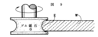
C.チャンファーはウエハーWの外周部を斜めに或いは丸く面取りするものである。チャンファーにレジンボンド砥石を使うと、先述のように外周部から割れたりクラックが入ったりする。特許文献3のテープ砥石を使うと時間がかかる。そこで割れやクラックを防ぐために本発明はゴム砥石を使う。
C. The chamfer chamfers the outer peripheral portion of the wafer W diagonally or roundly. If a resin bond grindstone is used for the chamfer, it will break or crack from the outer periphery as described above. When the tape grindstone of
ゴム砥石は、固定砥粒をゴムによって基盤に固定したものである。ウエハーに外接させて砥石を回転させてウエハーの外周部を傾斜面に或いは丸い曲面になるよう面取りする。 The rubber grindstone is a fixed abrasive grain fixed to a base with rubber. The wafer is circumscribed and the grindstone is rotated to chamfer the outer peripheral portion of the wafer into an inclined surface or a rounded curved surface.
図9は円曲面を持つ鼓型ゴム砥石GによってウエハーWの外周部(側面を含む)Eをチャンファーしている状態を示す。これは側面を含む外周部Eを丸く面取りする。 FIG. 9 shows a state where the outer peripheral portion (including the side surface) E of the wafer W is chamfered by the drum-shaped rubber grindstone G having a circular curved surface. This chamfers the outer peripheral part E including a side surface roundly.
図10は傾斜円錐面を持つ円錐台形型ゴム砥石Hによってウエハーの外周部Eをチャンファーしている様子を示す。これは上下縁を2回面取りする。角型に傾斜した面取りをする。 この場合は、ウエハーの側面はチャンファーされない。なお、砥石の形状は上記鼓型、円錐台形に限定されず、小型の砥石を変位して外周加工を実施することにより、ウエハー外周部の面取り形状を形成しても良い。 FIG. 10 shows a state where the outer peripheral portion E of the wafer is chamfered by a truncated cone-shaped rubber grindstone H having an inclined conical surface. This chamfers the top and bottom edges twice. Chamfered into a square shape. In this case, the side surface of the wafer is not chamfered. The shape of the grindstone is not limited to the above-mentioned drum shape or frustoconical shape, and the chamfered shape of the outer peripheral portion of the wafer may be formed by displacing a small grindstone and performing the outer periphery processing.
チャンファーは初め600番手のゴム砥石を使う。次いで2000番手のゴム砥石を用いる。600番手のゴム砥石でチャンファーすると、外周部Eの面粗度がRa0.3μm程度になる。2000番手のゴム砥石でチャンファーするとウエハーの外周部がRa0.07μm程度の面粗度になる。これによって外周部Eは平滑になる。チャンファーによって外周部Eに加工変質層Mが生ずる。 Chamfer uses the 600th rubber wheel first. Next, use a 2000th rubber grindstone. When chamfered with a 600th rubber grindstone, the surface roughness of the outer peripheral portion E becomes about Ra 0.3 μm. When chamfered with a 2000-th rubber grindstone, the outer peripheral portion of the wafer has a surface roughness of about Ra 0.07 μm. As a result, the outer peripheral portion E becomes smooth. A work-affected layer M is generated on the outer peripheral portion E by the chamfer.
D.表面研削によって厚みが約600〜550μmであったウエハーWの厚みを500μm〜520μm程度にする。研削量は時間によって変えることができる。例えば580μmの厚みのウエハーを510μmまで表面研削すると約60分かかる。これによってウエハーWの表面に加工変質層Mが生ずる。 D. The thickness of the wafer W having a thickness of about 600 to 550 μm is reduced to about 500 to 520 μm by surface grinding. The amount of grinding can be changed with time. For example, it takes about 60 minutes to grind a wafer having a thickness of 580 μm to 510 μm. As a result, a work-affected layer M is formed on the surface of the wafer W.
E.研磨は、表面の粗研磨と仕上げ研磨よりなる。粗研磨と仕上げ研磨によって表面が平滑面となる。表面、外周部に加工変質層Mが存在する。加工変質層Mの厚みdは研削量によって異なるが10μm〜50μm程度である。 E. Polishing consists of rough polishing of the surface and finish polishing. The surface becomes smooth by rough polishing and finish polishing. A work-affected layer M exists on the surface and the outer periphery. The thickness d of the work-affected layer M varies depending on the grinding amount, but is about 10 μm to 50 μm.
F.ウエハー表面の加工変質層の除去は、メカノケミカルポリッシュ(MCP)、電解研磨、液相エッチング及び気相エッチング等の種々可能であるが、今回は、高温にした塩素を含むガスを使った気相エッチングによって加工変質層Mを除去した。表面(Ga面)は化学的にも物理的にも裏面(N面)より堅固であって、アルカリエッチングでは表面を腐食しにくい。そこで表面の加工変質層除去は気相エッチングによった。 F. The process-affected layer on the wafer surface can be removed by various methods such as mechanochemical polishing (MCP), electropolishing, liquid phase etching, and gas phase etching. The work-affected layer M was removed by etching. The surface (Ga surface) is stronger than the back surface (N surface) both chemically and physically, and the surface is hardly corroded by alkali etching. Therefore, removal of the work-affected layer on the surface was performed by vapor phase etching.
研削、エッチングの条件を変えてウエハー外周部の加工変質層Mの厚みdが異なるウエハーを幾つも作った。できたGaNウエハーの外周部加工変質層Mの厚みはd=0μm〜20μm程度である。 Several wafers having different thicknesses d of the work-affected layer M on the outer periphery of the wafer were prepared by changing the grinding and etching conditions. The thickness of the outer peripheral portion work-affected layer M of the resulting GaN wafer is about d = 0 μm to 20 μm.
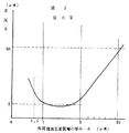
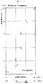
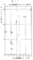
[2.外周部加工変質層厚みdと反りUの関係]
ウエハーの反りの表現方法は幾つかある。ウエハーの中心線の曲率半径Rとか、曲率1/Rとか、ウエハー中心の高さなどである。ここでは反りは2インチウエハー換算で平坦面にウエハーを置いたときの中心の高さUで表している。
[2. Relationship between outer peripherally processed deteriorated layer thickness d and warpage U]
There are several ways to express wafer warpage. The curvature radius R of the center line of the wafer, the
図13に定義を示す。U=D2/8Rの関係がある。Dはウエハーの直径で、Rは曲率半径である。ウエハーの反りUをそれぞれ測定した。 The definition is shown in FIG. There is a relationship of U = D 2 / 8R. D is the diameter of the wafer and R is the radius of curvature. Wafer warpage U was measured.
そこで、ウエハー外周部の加工変質層Mの厚みdを変数として、反りUとの関係を調べた。その結果を図2に示す。横軸は外周部加工変質層厚みd(μm)を対数表示したものである。縦軸は反りU(μm)である。 Accordingly, the relationship with the warp U was examined using the thickness d of the work-affected layer M on the outer periphery of the wafer as a variable. The result is shown in FIG. The horizontal axis is a logarithmic representation of the outer peripherally processed deteriorated layer thickness d (μm). The vertical axis represents warpage U (μm).
他にも様々な因子があるが、反りUが外周部加工変質層厚みdのほぼ一価の関数で表されるということが分かる。反りUは外周部加工変質層厚みdが3μm〜20μmの範囲で単調に増加することが分かった。d=10μmで反りは50μmになる。d=0.5μm〜10μmで反りは50μm未満である。3μm〜1μmで極小となる。外周部加工変質層厚みdが1μmより薄くなると反りが却って大きくなる傾向が見られた。 Although there are various other factors, it can be seen that the warpage U is expressed by a substantially monovalent function of the outer peripheral portion work-affected layer thickness d. It has been found that the warpage U increases monotonously in the range of 3 μm to 20 μm in the outer peripheral part work-affected layer thickness d. When d = 10 μm, the warpage is 50 μm. When d = 0.5 μm to 10 μm, the warpage is less than 50 μm. It becomes minimum at 3 μm to 1 μm. When the thickness d of the outer peripheral portion processed deteriorated layer was thinner than 1 μm, the warp tended to increase on the contrary.
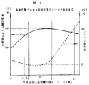
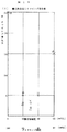
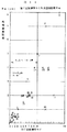
[3.外周部加工変質層厚みdとクラック発生率Cの関係]
ウエハーのクラック発生率Cも調べた。図3にその結果を示す。図3の横軸は外周部加工変質層厚みdで、右縦軸はクラック発生率C(%)である。破線がクラック発生率を示す。クラックは様々な因子によって起こるが、これも外周部加工変質層の厚みdとほぼ一義的な関係があることが分かった。
[3. Relationship between thickness d of outer peripherally processed layer and crack occurrence rate C]
The crack generation rate C of the wafer was also examined. The result is shown in FIG. The horizontal axis in FIG. 3 is the outer peripheral part work-affected layer thickness d, and the right vertical axis is the crack occurrence rate C (%). The broken line indicates the crack occurrence rate. Although cracks occur due to various factors, it has been found that this also has a substantially unambiguous relationship with the thickness d of the outer peripheral portion work-affected layer.
クラック発生率C(%)は外周部加工変質層厚みdが3μm〜10μmの範囲で単調に増大する。1μm→0μmでクラック発生率が上昇する。d=0.5μm〜10μmでクラック発生率を50%以下にできる。クラック発生を極小にする外周部加工変質層の厚みdは3μm以下である。 The crack occurrence rate C (%) monotonously increases in the range where the outer peripheral part work-affected layer thickness d is 3 μm to 10 μm. The crack generation rate increases from 1 μm to 0 μm. When d = 0.5 μm to 10 μm, the crack generation rate can be reduced to 50% or less. The thickness d of the outer peripheral work-affected layer that minimizes the occurrence of cracks is 3 μm or less.
[4.外周部加工変質層厚みdと基板作製プロセス歩留まりYの関係]
基板作製プロセスの歩留まりY(%)も調べた。ウエハー(基板)作製の出来映えは多様な因子によって左右されるが、基板作製プロセス歩留まりYは外周部加工変質層の厚みdとほぼ一義的な関係があるということが分かった。
[4. Relationship between thickness d of outer peripheral work-affected layer and substrate production process yield Y]
The yield Y (%) of the substrate manufacturing process was also examined. Although the performance of wafer (substrate) fabrication depends on various factors, it has been found that the substrate fabrication process yield Y is almost uniquely related to the thickness d of the outer peripheral work-affected layer.
図3の実線の曲線が基板作製プロセス歩留まりと外周部加工変質層厚みdの関係を示す。基板作製プロセス歩留まりYは外周部加工変質層厚みdが3μm〜10μmの間で80%〜75%程度である。d=0.5μm〜10μmで基板作製プロセス歩留まりYは72〜80%である。d=10μmで76%である。10μm〜20μmではもっと落ちるので図示していない。 The solid curve in FIG. 3 shows the relationship between the yield of the substrate manufacturing process and the outer peripheral portion work-affected layer thickness d. The substrate manufacturing process yield Y is about 80% to 75% when the outer peripheral part work-affected layer thickness d is between 3 μm and 10 μm. When d = 0.5 μm to 10 μm, the substrate manufacturing process yield Y is 72 to 80%. It is 76% at d = 10 μm. 10 μm to 20 μm is not shown in the figure because it falls more.
外周部加工変質層厚みdが1μmで基板作製プロセス歩留まりYが75%程度に低下する。dが0μmへ下がると基板作製プロセス歩留まりYが60%程度に低下する。
基板作製プロセス歩留まりYを72〜80%に維持するには0.5μm〜10μm程度の外周部加工変質層厚みdが適している。
The substrate manufacturing process yield Y is reduced to about 75% when the outer peripheral portion work-affected layer thickness d is 1 μm. When d decreases to 0 μm, the substrate manufacturing process yield Y decreases to about 60%.
In order to maintain the substrate manufacturing process yield Y at 72 to 80%, an outer peripherally processed deteriorated layer thickness d of about 0.5 μm to 10 μm is suitable.
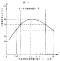
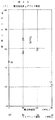
[5.外周部加工変質層厚みdとデバイス面内歩留まりQの関係]
ウエハーの上に発光素子などのデバイスを作製してデバイスの面内歩留まりQも調べた。デバイス面内歩留まりQもウエハーの外周部加工変質層Mの厚みdと強い関係があることが分かった。
[5. Relationship between thickness d of outer peripherally processed layer and device yield Q]
A device such as a light emitting element was fabricated on the wafer, and the in-plane yield Q of the device was also examined. It was found that the device in-plane yield Q is also strongly related to the thickness d of the outer peripherally processed layer M of the wafer.
図4に測定結果を示す。厚みdが1.7μm程度で極大の80%程度となる。dが3μmを越えるとデバイス面内歩留まりQは低下していく。反対に外周部加工変質層厚みdが0μmに近づくとデバイス面内歩留まりQは50%を経て40%以下に急激に低下する。デバイス面内歩留まりQを60%以上にするには外周部加工変質層の厚みdを0.5μm〜10μm程度にしなければならない。デバイス面内歩留まりQを70%以上にするにはdを1μm〜5μm程度にしなければならない。 FIG. 4 shows the measurement results. The thickness d is about 1.7 μm, which is about 80% of the maximum. When d exceeds 3 μm, the device in-plane yield Q decreases. On the contrary, when the outer peripheral portion work-affected layer thickness d approaches 0 μm, the device in-plane yield Q rapidly decreases to 40% or less after 50%. In order to increase the device surface yield Q to 60% or more, the thickness d of the outer peripheral portion work-affected layer must be about 0.5 μm to 10 μm. In order to increase the device surface yield Q to 70% or more, d must be about 1 μm to 5 μm.
外周部加工変質層厚みd=0μmが良いように思えるが、上の結果からはそうではないことが分かる。d=0.5μm〜10μm、特に望ましくは1〜3μmの外周部加工変質層が残留しているのが良いということが明らかになる。 Although it seems that the outer peripherally processed deteriorated layer thickness d = 0 μm is good, the above results show that this is not the case. It becomes clear that it is preferable that the outer peripheral part work-affected layer of d = 0.5 μm to 10 μm, particularly preferably 1 to 3 μm, remains.
反りU、基板作製プロセス歩留まりY、クラック発生率C、デバイス面内歩留まりQの全てを勘案し、表面に残留する外周部加工変質層Mの厚みdは1μm〜3μmにするのが良いということが分かる。
上記は2インチのGaNウエハーに対して、裏面研削、裏面エッチング、外周研削、表面研削、表面研磨、気相エッチングを実施した場合について記載した。GaNインゴットからスライスしてウエハーを得て、裏面エッチング、外周研削、表面研磨、気相エッチングを実施した場合についても、同じ結果が得られた。
上記はGaNウエハーについて記載したが、AlNやAlGaNあるいはInGaNなどの窒化物ウエハーでも同じ結果が得られた。
Considering all of the warpage U, the substrate manufacturing process yield Y, the crack occurrence rate C, and the device in-plane yield Q, it is preferable that the thickness d of the outer peripheral work-affected layer M remaining on the surface be 1 μm to 3 μm. I understand.
The above describes the case where backside grinding, backside etching, peripheral grinding, surface grinding, surface polishing, and vapor phase etching are performed on a 2-inch GaN wafer. The same result was obtained when a wafer was obtained by slicing from a GaN ingot, and back surface etching, peripheral grinding, surface polishing, and vapor phase etching were performed.
Although the above has been described for GaN wafers, similar results were obtained with nitride wafers such as AlN, AlGaN or InGaN.
本発明はそのような結果の堆積に基づいて、気相成長したアズグロウンの窒化物半導体ウエハーを裏面研削、チャンファー、表面研削研磨してミラーウエハーに加工する際、ゴム砥石或いは発泡樹脂砥石でチャンファーしウエハー外周部の加工変質層を0.5μm〜10μm、より好ましくは1μm〜3μm残留させるという手法を提案する。 Based on the accumulation of such results, the present invention uses a rubber grindstone or a foamed resin grindstone to process a vapor-grown as-grown nitride semiconductor wafer into a mirror wafer by back grinding, chamfering, and surface grinding. A method is proposed in which the work-affected layer on the outer periphery of the wafer is left to remain in the range of 0.5 μm to 10 μm, more preferably 1 μm to 3 μm.
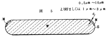
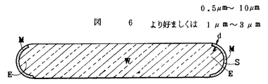
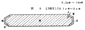
図5〜図8はそのような手法で作製された窒化物半導体ウエハーWの概略の断面図を示す。 5 to 8 are schematic cross-sectional views of the nitride semiconductor wafer W manufactured by such a method.
図5は円形研磨面を持つ鼓型ゴム砥石(G)でチャンファーしたウエハーの表面の加工変質層Mを完全に除去し、外周部に0.5μm〜10μm、好ましくは1μm〜3μmの加工変質層Mを残留させている。 FIG. 5 shows that the work-affected layer M on the surface of the wafer chamfered with a drum-shaped rubber grindstone (G) having a circular polished surface is completely removed, and the work-affected layer is 0.5 μm to 10 μm, preferably 1 μm to 3 μm in the outer periphery. Layer M remains.
図6は円形研磨面を持つ鼓型ゴム砥石(G)でチャンファーしたウエハーの表面の加工変質層Mを完全に除去し、外周部(側面を含む)に0.5μm〜10μm、好ましくは1μm〜3μmの加工変質層Mを残留させている。 FIG. 6 shows that the work-affected layer M on the surface of the wafer chamfered with a drum-type rubber grindstone (G) having a circular polished surface is completely removed, and 0.5 μm to 10 μm, preferably 1 μm, on the outer peripheral portion (including the side surface). A work-affected layer M of ˜3 μm remains.
図7は傾斜円錐面を持つ円錐台形型ゴム砥石(H)でチャンファーしたウエハーの表面及び側面の加工変質層Mを完全に除去し、外周部に0.5μm〜10μm、好ましくは1μm〜3μmの加工変質層Mを残留させている。 FIG. 7 shows that the wafer surface and side surface modified layer M chamfered with a frustoconical rubber grindstone (H) having an inclined conical surface is completely removed, and the outer peripheral portion is 0.5 μm to 10 μm, preferably 1 μm to 3 μm. The work-affected layer M is left.
図8は傾斜円錐面を持つ円錐台形型ゴム砥石(H)でチャンファーしたウエハーの表面の加工変質層Mを完全に除去し、外周部(側面を含む)に0.5μm〜10μm好ましくは1μm〜3μmの加工変質層Mを残留させている。 FIG. 8 shows that the work-affected layer M on the surface of the wafer chamfered with a frustoconical rubber grindstone (H) having an inclined conical surface is completely removed, and 0.5 μm to 10 μm, preferably 1 μm, on the outer periphery (including the side surface). A work-affected layer M of ˜3 μm remains.
[実施例2;試料1〜11、表1;図14、15、16]
チャンファーはウエハーが大口径になるほど困難になる。クラック、反りの問題が生じやすく、半導体デバイスを形成した際に、歩留まりが低下しやすい。本発明が大口径ウエハーに適用可能であれば有用性は一層増大する。
[Example 2;
The chamfer becomes more difficult as the wafer becomes larger. Cracks and warpage are likely to occur, and the yield tends to decrease when a semiconductor device is formed. If the present invention is applicable to a large-diameter wafer, the usefulness is further increased.
そこで実施例2〜4では、直径5インチ厚み850μmの大口径大厚みのGaNウエハーに1段階チャンファーを行った26例を述べる。5インチ径GaNウエハーは本発明が初めて提案するもので類例がない。図14〜図24に数字で試料番号を印した。○は合格、×は不合格の試料である。窒化ガリウムウエハーの加工のうち、試料1〜26の全てに共通である工程についてここで説明する。
Therefore, in Examples 2 to 4, 26 examples in which a one-step chamfer is performed on a GaN wafer having a large diameter and a thickness of 850 μm and a large diameter and a thickness of 850 μm will be described. A 5-inch diameter GaN wafer is proposed by the present invention for the first time and is unparalleled. The sample numbers are marked with numerals in FIGS. ○ is a pass sample and × is a reject sample. Of the processing of the gallium nitride wafer, steps common to all of the
[GaN基板の加工]
図1の工程図に示すように、GaNウエハーの裏面研削(A)をし、それによって裏面にできた加工変質層をKOHで除去し(B)、外周部を加工(C;チャンファー加工:研削の一種)し、表面を研削し(D)、表面を研磨し(E)、表面にできた加工変質層を気相エッチング(F)で除去する工程を行なう。本発明はCのチャンファーに特徴があるが全工程A〜Fを説明する。
[Processing of GaN substrate]
As shown in the process diagram of FIG. 1, the back surface grinding (A) of the GaN wafer is performed, the work-affected layer formed on the back surface is removed by KOH (B), and the outer peripheral portion is processed (C; chamfer processing: A kind of grinding), the surface is ground (D), the surface is polished (E), and the work-affected layer formed on the surface is removed by vapor phase etching (F). Although the present invention is characterized by C chamfer, all steps A to F will be described.
(1)GaN基板の成形加工
HVPE法により成長させた直径5インチ(127mm)のn型GaNインゴット(ドーパント:O)をワイヤーソーで(0001)面に平行な面で切り出して厚さ850μmの基板を得た。得られた基板に対して裏面研削を行った(工程A)。研削は#600のダイヤモンド砥石を用いた。研削によって裏面に加工変質層ができた。研削後に濃度15%のKOH水溶液で50℃のエッチングを実施し加工変質層を除去した(工程B)。裏面のエッチングは、エッチング速度が十分あれば、NaOH、H3PO4等の、その他のアルカリ、酸の水溶液を用いることができる。また、ドライエッチングでの加工変質層除去も可能であった。エッチング後の基板について、表1に示す砥石を用いて、GaN基板の面取り加工(工程C)を実施した。その後に表面の研磨加工を実施した。
(1) GaN substrate molding
An n-type GaN ingot (dopant: O) having a diameter of 5 inches (127 mm) grown by the HVPE method was cut out with a wire saw in a plane parallel to the (0001) plane to obtain a substrate having a thickness of 850 μm. Back grinding was performed on the obtained substrate (Step A). A # 600 diamond grinding wheel was used for grinding. A work-affected layer was formed on the back surface by grinding. After grinding, etching was performed at 50 ° C. with a 15% strength KOH aqueous solution to remove the work-affected layer (step B). For the etching of the back surface, if the etching rate is sufficient, an aqueous solution of other alkali or acid such as NaOH or H 3 PO 4 can be used. In addition, the work-affected layer can be removed by dry etching. About the board | substrate after an etching, the chamfering process (process C) of the GaN board | substrate was implemented using the grindstone shown in Table 1. FIG. The surface was then polished.
(2)GaN基板表面のラップ、CMP(化学機械研磨)
GaN基板(窒化物結晶)のN原子面側のC面(裏面;(000−1)面)をセラミック製の結晶ホルダ−にワックスで取り付けた。ラップ装置に直径600mmの定盤を設置し、スラリー供給口からダイヤモンドの遊離砥粒が分散されたスラリーを定盤に供給しながら、定盤をその回転軸を中心に回転させ、結晶ホルダ−上に重りを載せることにより、GaN基板表面を定盤に押しつけながらGaN基板を結晶ホルダ−の回転軸を中心にして回転させ、n型GaNの表面(Ga原子面側;C面(0001)面)のラッピングを行った。
(2) Lapping of GaN substrate surface, CMP (Chemical Mechanical Polishing)
The C surface (back surface; (000-1) surface) on the N atom surface side of the GaN substrate (nitride crystal) was attached to a ceramic crystal holder with wax. Install a surface plate with a diameter of 600 mm on the lapping machine, and rotate the surface plate around its axis of rotation while supplying slurry with free abrasive grains of diamond dispersed from the slurry supply port to the surface of the crystal holder. By placing a weight on the n-type GaN surface (Ga atom plane side; C plane (0001) plane), the GaN substrate is rotated around the rotation axis of the crystal holder while pressing the GaN substrate surface against the surface plate. Wrapping was done.
ここで定盤としては、銅定盤、錫定盤を用いた。砥粒粒径が9μm、3μm、2μmの3種類のダイヤモンド砥粒(遊離砥粒)を準備し、ラッピングの進行とともに砥粒径を段階的に小さくしていった。研磨圧力は100g/cm2〜500g/cm2とした。GaN基板及び定盤の回転数は何れも30回/min〜60回/minとした。かかるラッピングによりGaN結晶基板の表面は鏡面になった。 Here, a copper surface plate and a tin surface plate were used as the surface plate. Three types of diamond abrasive grains (free abrasive grains) having an abrasive grain diameter of 9 μm, 3 μm, and 2 μm were prepared, and the abrasive grain diameter was gradually reduced as lapping progressed. Polishing pressure was 100g / cm 2 ~500g / cm 2 . The rotational speeds of the GaN substrate and the surface plate were both 30 times / min to 60 times / min. By such lapping, the surface of the GaN crystal substrate became a mirror surface.
ポリッシュ装置に設置された直径600mmの定盤上にポリシングパッドを設置し、スラリー液供給口から砥粒が分散されたスラリーをポリシングパッドに供給しながら、回転軸を中心にしてポリシングパッドを回転させると共に、結晶ホルダ−上に重りを載せることにより、GaN基板をポリシングパッドに押しつけながらGaN基板を結晶ホルダ−の回転軸を中心として回転させ、GaNの表面(Ga原子面のC面(0001)面)のCMP(化学機械研磨)を行った。 A polishing pad is installed on a surface plate having a diameter of 600 mm installed in the polishing apparatus, and the polishing pad is rotated around the rotation axis while supplying slurry in which abrasive grains are dispersed from the slurry liquid supply port to the polishing pad. At the same time, by placing a weight on the crystal holder, the GaN substrate is rotated about the rotation axis of the crystal holder while pressing the GaN substrate against the polishing pad, and the surface of GaN (the C plane (0001) plane of the Ga atomic plane) ) CMP (chemical mechanical polishing).
スラリーは、砥粒として粒径2μmのAl2O3粒子を水に分散させてAl2O3含有量を5質量%とし、pH調整剤としてHNO3を添加して、pHを2〜4に調整することにより作製した。また、ポリシングパッドとしては、ポリウレタンのスエードパッドを用いた。定盤としてはステンレス鋼定盤を用いた。ポリシング圧力は50g/cm2〜600g/cm2とした。GaN基板及びポリシングパッドの回転数はいずれも30回/min〜70回/minとした。 In the slurry, Al 2 O 3 particles having a particle diameter of 2 μm are dispersed in water as abrasive grains to make the Al 2 O 3 content 5 mass%, HNO 3 is added as a pH adjuster, and the pH is adjusted to 2 to 4 It was prepared by adjusting. A polyurethane suede pad was used as the polishing pad. A stainless steel surface plate was used as the surface plate. Policing pressure was 50g / cm 2 ~600g / cm 2 . The rotational speeds of the GaN substrate and the polishing pad were both 30 times / min to 70 times / min.
(3)GaN基板の表面のドライエッチ、洗浄
CMP処理を行った基板について、塩素含有ガスを用いて、ICP−RIE装置でドライエッチングを実施した。エッチングガスには塩素を用いた。
ドライエッチング処理を行った基板について、希釈KOH水溶液とIPA(イソプロピルアルコール)で洗浄を実施した。最終状態の基板について、加工変質層、粗さ、反り、酸素量、金属量、チッピングの評価を行った。表面の粗さはいずれもRa1.5nmであった。裏面の粗さはいずれもRa5.6μmであった。他の結果を表1、2、3に示す。
(3) Dry etching and cleaning of the surface of the GaN substrate
The substrate subjected to the CMP treatment was dry-etched with an ICP-RIE apparatus using a chlorine-containing gas. Chlorine was used as the etching gas.
The substrate subjected to the dry etching treatment was washed with a diluted KOH aqueous solution and IPA (isopropyl alcohol). The substrate in the final state was evaluated for a work-affected layer, roughness, warpage, oxygen content, metal content, and chipping. The surface roughness was Ra 1.5 nm. The roughness of the back surface was Ra 5.6 μm. Other results are shown in Tables 1, 2, and 3.
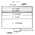
(4)n型GaN基板を含むLEDデバイス
n型GaN基板は、比抵抗1×10⁻²Ωcm、キャリヤ密度3×10¹⁸/cm3のものを用いた。n型GaN基板をMOCVD装置内に設置し、n型GaN基板の表面((0001)面)側に、MOCVD法により、厚さ1μmのn型GaN層(ドーパント:Si)、厚さ150nmのn型Al0.1Ga0.9N層(ドーパント:Si)、発光層、厚さ20nmのp型Al0.2Ga0.8N(ドーパント:Mg)および厚さ150nmのp型GaN層(ドーパント:Mg)を順次形成しエピタキシャルウエハーを得た。これの1素子分を図25に示す。発光層は、厚さ10nmのGaN層で形成される障壁層の4層と、厚さ3nmのGa0.85In0.15N層で形成される井戸層の3層が交互に積層された多重量子井戸構造とした。
(4) LED device including an n-type GaN substrate
An n-type GaN substrate having a specific resistance of 1 × 10 −2 Ωcm and a carrier density of 3 × 10 18 / cm 3 was used. An n-type GaN substrate is placed in an MOCVD apparatus, and an n-type GaN layer (dopant: Si) having a thickness of 1 μm and an n-type having a thickness of 150 nm are formed on the surface ((0001) plane) side of the n-type GaN substrate by MOCVD. Type Al 0.1 Ga 0.9 N layer (dopant: Si), light emitting layer, 20 nm thick p-type Al 0.2 Ga 0.8 N (dopant: Mg) and 150 nm thick p-type GaN layer ( An epitaxial wafer was obtained by sequentially forming a dopant: Mg). One element of this is shown in FIG. The light-emitting layer was formed by alternately laminating four layers of a barrier layer formed of a GaN layer having a thickness of 10 nm and three layers of a well layer formed of a Ga 0.85 In 0.15 N layer having a thickness of 3 nm. A multiple quantum well structure was adopted.
つぎにn型のGaN結晶基板の他方の裏面((000−1)面、N面)に第1の電極として、厚さ200nmのTi層、厚さ1000nmのAl層、厚さ200nmのTi層、厚さ2000nmのAu層から形成される積層構造を形成し、窒素雰囲気中で加熱することにより、直径100μmのn側電極を形成した。一方p型GaN層上に第2の電極として、厚さ4nmのNi層、厚さ4nmのAu層から形成される積層構造を形成し、不活性ガス雰囲気中で加熱することにより、p側電極を形成した。図26に電極を形成した一素子分のウエハーの断面図を示す。上記半導体ウエハーを2mm角にチップ化した後に、上記p側電極をAuSnで形成された半田層でステムにボンディングした。さらに、上記n側電極をリードピンとワイヤでボンディングして、LEDとしての構成を有する半導体デバイスを得た(図27)。 Next, a Ti layer having a thickness of 200 nm, an Al layer having a thickness of 1000 nm, and a Ti layer having a thickness of 200 nm are formed as first electrodes on the other back surface ((000-1) plane, N plane) of the n-type GaN crystal substrate. A laminated structure formed of an Au layer having a thickness of 2000 nm was formed, and heated in a nitrogen atmosphere to form an n-side electrode having a diameter of 100 μm. On the other hand, a laminated structure formed of a 4 nm thick Ni layer and a 4 nm thick Au layer is formed as a second electrode on the p-type GaN layer, and heated in an inert gas atmosphere, whereby a p-side electrode is formed. Formed. FIG. 26 shows a sectional view of a wafer for one element on which an electrode is formed. After the semiconductor wafer was chipped into 2 mm square, the p-side electrode was bonded to the stem with a solder layer formed of AuSn. Further, the n-side electrode was bonded with a lead pin and a wire to obtain a semiconductor device having a configuration as an LED (FIG. 27).
エピダウンであるのは、GaN基板が透明であるから基板側から光を出すことができ、しかも発熱する発光層がステムに近く熱伝導によってステムからパッケージを通じて放熱できるからである。サファイヤ基板(40W/mK)よりGaNは熱伝導率(210W/mK)が約5倍高くて基板を通って上部からも放熱が促進される。GaN基板の優れた特長を遺憾なく発揮できる。得られたLEDの光出力を、注入電流4Aの条件で積分球を用いて測定した。電流を流すと素子の発光層から周りに光が出る。一部の光が上向きに出て基板を通り外部へ出る。一部の光は下向きに出てステムで反射されて外部へ出る。パッケージ側面に当たった光も上向きに反射されて外部へ出る。2mm角の大きいチップで、エピダウンで固定され下向き光も上へ反射されるから大出力の発光素子となる。 Epidown is because the GaN substrate is transparent, so that light can be emitted from the substrate side, and the light-emitting layer that generates heat is close to the stem and can dissipate heat from the stem through the package. GaN has a thermal conductivity (210 W / mK) that is about five times higher than that of the sapphire substrate (40 W / mK), and heat dissipation is promoted from above through the substrate. The excellent features of the GaN substrate can be demonstrated without regret. The light output of the obtained LED was measured using an integrating sphere under the condition of an injection current of 4A. When an electric current is passed, light is emitted from the light emitting layer of the element. A part of the light goes upward and goes out through the substrate. Some light exits downward, is reflected by the stem, and exits. The light hitting the side of the package is also reflected upward and goes out. A large 2 mm square chip is fixed in an epi-down, and downward light is reflected upward.
発光素子の光出力は以下のように測定した。積分球内に配置された発光素子に所定の電流(4A)を注入し、その発光素子から出た殆ど全ての光を積分球で集め集光点に置いたディテクタに集光された光パワーを測定した。LEDとしては、光出力が大きい方が高性能なデバイスとなる。光出力が2W以上で良好な特性と判断し、2W未満だと不良と判定した。以上の加工、デバイス作製、検査は試料1〜26に共通である。
The light output of the light emitting element was measured as follows. A predetermined current (4A) is injected into the light emitting element arranged in the integrating sphere, almost all the light emitted from the light emitting element is collected by the integrating sphere, and the light power condensed on the detector placed at the condensing point is obtained. It was measured. As an LED, a device having a higher light output is a higher performance device. When the optical output was 2 W or more, it was judged as a good characteristic, and when it was less than 2 W, it was judged as defective. The above processing, device fabrication, and inspection are common to the
試料1〜11はダイヤ砥粒番手、ボンド材、酸化物比率を様々に変えて外周部の加工変質層厚みを多様にし、反り、クラック、デバイス歩留まりを調べた。
In
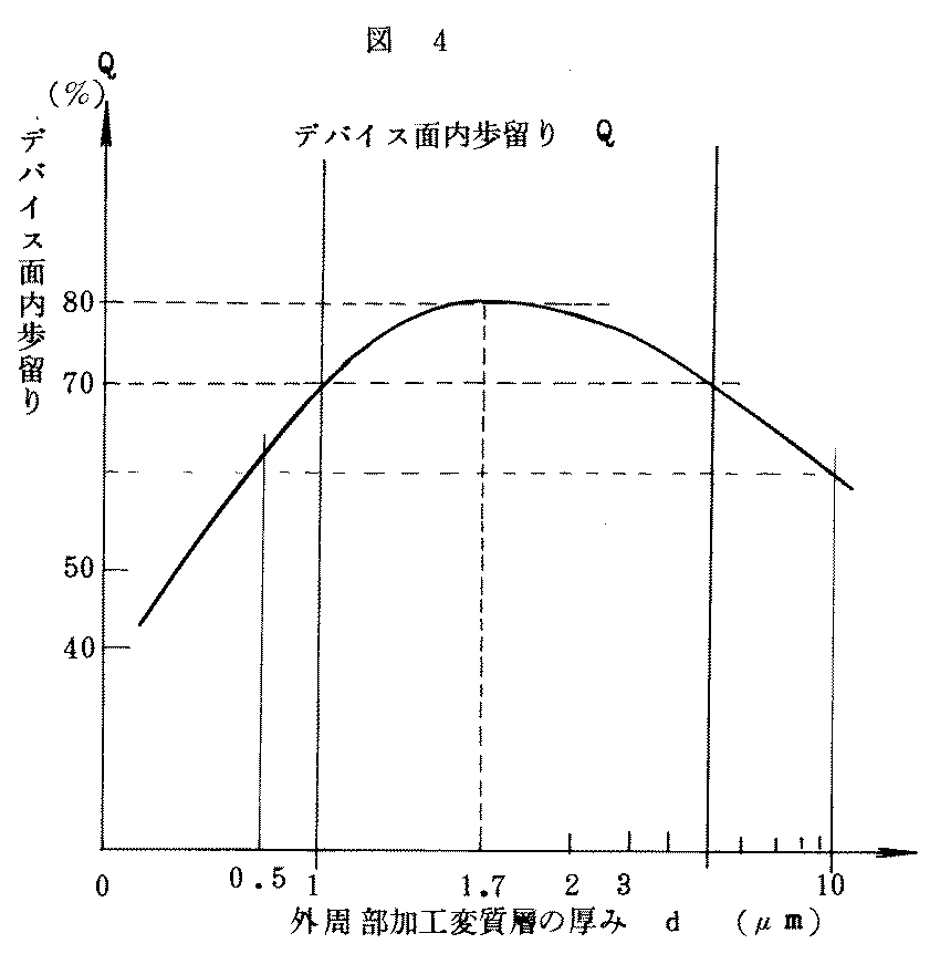
表1の最上欄は試料番号である。試料番号は1から11まである。基板特性はウエハー毎に測定した値である。試料毎に外周加工、基板特性、デバイス特性について表にしてある。 The top column of Table 1 is the sample number. Sample numbers are from 1 to 11. The substrate characteristics are values measured for each wafer. For each sample, the outer periphery processing, the substrate characteristics, and the device characteristics are tabulated.
表1の2行目から下の外周加工と記した部分が、加工に用いる砥石の物性を示す。外周加工は研削であり、砥粒を固定した砥石を回転させ、外周に接触させて行う。ボンドというのは砥粒を基盤に固定する材料である。通常、砥石としては樹脂や金属によって砥粒を固定するレジンボンド、メタルボンド砥石あるいは砥粒を電着した電着砥石が頻用される。しかし本発明ではレジンボンド砥石、メタルボンド砥石、電着砥石などを用いない。これらは砥粒を基盤に剛直固定してしまうので望ましくない。 The part described as the outer periphery processing from the second line of Table 1 shows the physical properties of the grindstone used for processing. The outer periphery processing is grinding, and is performed by rotating a grindstone on which abrasive grains are fixed and contacting the outer periphery. A bond is a material that fixes abrasive grains to a substrate. Usually, a resin bond, a metal bond grindstone, or an electrodeposited grindstone electrodeposited with abrasive grains is frequently used as the grindstone. However, in the present invention, a resin bond grindstone, a metal bond grindstone, an electrodeposition grindstone or the like is not used. These are not desirable because the abrasive grains are rigidly fixed to the base.
本発明はゴムボンド砥石、発泡レジンボンド砥石によって外周加工(研削)する。比較のためレジンボンド砥石、メタルボンド砥石、電着砥石によっても外周加工した。材質の欄はボンド材料の材質を示す。CRというのはクロロプレンゴム(chloroprene rubber)のことである。ゴムボンドの硬度をつぎの欄に示す。レジンボンド、メタルボンドの場合はもっと硬度が高く測定方法が異なる。樹脂(レジン)そのものだとなお弾力性に乏しく不可なので、樹脂を発泡させてさらに弾力性を高めると有用になる。発泡させるとレジンと気泡の複合物になる。気孔の体積比率を空孔率(体積%)という。空孔率で柔軟性を評価できる。 In the present invention, outer periphery processing (grinding) is performed by a rubber bond grindstone and a foamed resin bond grindstone. For comparison, the outer periphery was also processed with a resin bond grindstone, a metal bond grindstone, and an electrodeposition grindstone. The column of material indicates the material of the bond material. CR refers to chloroprene rubber. The hardness of the rubber bond is shown in the next column. Resin bonds and metal bonds have higher hardness and different measurement methods. Resin itself is still poor in elasticity and impossible, so it is useful to further increase elasticity by foaming the resin. When foamed, it becomes a composite of resin and bubbles. The volume ratio of pores is referred to as porosity (volume%). Flexibility can be evaluated by porosity.
表中に酸化物砥粒の種類とその重量%を示す。100%から酸化物砥粒の重量%を引いたものがダイヤモンド砥粒の重量%である。 The types of oxide abrasive grains and their weight percentages are shown in the table. The weight percentage of diamond abrasive grains is 100% minus the weight percentage of oxide abrasive grains.
基板特性の欄には、外周加工後の4つの基板の特性を示す。一番目は外周部の加工変質層の厚さ(μm)である。CL(カソードルミネセンス)によって加工変質層の部分を他の部分と区別できる。外周部に残った加工変質層の厚さをCLによって測定する。二番目の欄は表面粗さ(Ra)でμmが単位である。3番目の欄は基板の反りで、平坦面に外周部が接するようウエハーを置いたときの中央部の高さHで反りを表現する。広い面積(大きい直径)をもつウエハーであるから高さで表した反りの値は大きいが曲率で表現するとかなり小さい。二次関数で反りを近似したとすると曲率半径がRでウエハーの直径をDとすると中央部の高さをUとして、R=D2/8Uである。たとえば反り高さU=20μmとすると、D=127mmとして、R=100mである。曲率に直すと1/R=0.01m−1である。 In the column of the substrate characteristics, the characteristics of the four substrates after the outer periphery processing are shown. The first is the thickness (μm) of the work-affected layer at the outer periphery. Parts of the work-affected layer can be distinguished from other parts by CL (cathode luminescence). The thickness of the work-affected layer remaining on the outer periphery is measured by CL. The second column is the surface roughness (Ra) in μm. The third column shows the warpage of the substrate, and the warpage is expressed by the height H of the central portion when the wafer is placed so that the outer peripheral portion is in contact with the flat surface. Since the wafer has a large area (large diameter), the warp value expressed in height is large, but it is considerably small when expressed in curvature. If the curvature is approximated by a quadratic function, if the radius of curvature is R and the diameter of the wafer is D, the height of the central portion is U, and R = D 2 / 8U. For example, if the warp height U = 20 μm, D = 127 mm and R = 100 m. In terms of curvature, 1 / R = 0.01 m −1 .
クラックというのは、外周研削中にウエハーが欠けたり割れたりするというものである。クラック発生率というのは、同じ条件の試料ウエハーのうち研削中に欠け割れが生じたものの枚数の全体の枚数に対する比である。試料1〜11は様々の条件で外周研削し、後のウエハーの反り、クラック発生率、デバイス歩留まりを試験したものである。
A crack means that a wafer is chipped or cracked during peripheral grinding. The crack occurrence rate is the ratio of the number of sample wafers having the same conditions to which the cracks occurred during grinding to the total number.
デバイスの欄では1枚のGaNウエハーから取れた素子のうちの良好なものの比率を歩留まりとして示す。素子は大型の発光ダイオードで2mm角のチップ(面積4mm2)である。通常製造販売される汎用発光ダイオードは300μm〜500μm角である。それらに比べて15倍〜40倍の面積をもつ大きい発光ダイオードである。直径127mmのウエハーの面積は約12000mm2であるから、チップ約3000個分の面積がある。チップをサンプリングしてパッケージに収容し、通電試験して歩留まりを調べた。面積(2mm角)が大きいので確率論的に通常の面積のチップ(0.3〜0.5mm角)より歩留まりは低くなるが、それでもかなり高い歩留まりで良好な大型発光ダイオードを製造することができた。
In the device column, the ratio of good elements out of one GaN wafer is shown as a yield. The element is a large light-emitting diode and is a 2 mm square chip (
図14は試料1〜11について加工変質層厚みd(μm)とウエハー反りU(μm)の関係を示すグラフである。図中の数字は試料番号を表す。矢印で示すd=0.5μm〜10μmというのは本発明で提案するdの範囲である。矢印で示すd=1〜3μmというのは特に望ましい範囲である。図15は試料1〜11について加工変質層厚みd(μm)とクラック発生率C(%)の関係を示すグラフである。図16は試料1〜11について加工変質層厚みd(μm)とデバイス歩留まりQ(%)の関係を示すグラフである。 FIG. 14 is a graph showing the relationship between the work-affected layer thickness d (μm) and the wafer warpage U (μm) for Samples 1-11. The numbers in the figure represent sample numbers. D = 0.5 μm to 10 μm indicated by an arrow is a range of d proposed in the present invention. D = 1-3 μm indicated by an arrow is a particularly desirable range. FIG. 15 is a graph showing the relationship between the work-affected layer thickness d (μm) and the crack occurrence rate C (%) for Samples 1-11. FIG. 16 is a graph showing the relationship between the work-affected layer thickness d (μm) and the device yield Q (%) for Samples 1-11.
[試料1(Fe2O3;ゴム砥石;d=0.3μm;Q=52%)]
5インチ直径(127mm)で850μm厚みの円形GaNウエハーを裏面研削(A)、裏面エッチング(B)の後、クロロプレンゴム(CR)をボンディング材料とするゴム砥石を用いて外周研削した(チャンファーC)。砥粒を基板に固定するボンディング材にゴムを使うのでゴムボンド砥石というべきであろうが簡単にゴム砥石と呼ぶ。かといってゴムで研削するのでなく研削材の主体はダイヤモンド砥粒である。ボンディング材のゴムは発泡できないので空孔率は0%である(レジンボンドの場合は発泡可能である)。ゴムは配合比によって硬度を変化させることができる。このゴム砥石のゴム硬度は40である。
[Sample 1 (Fe 2 O 3 ; rubber grindstone; d = 0.3 μm; Q = 52%)]
A circular GaN wafer having a diameter of 5 inches (127 mm) and a thickness of 850 μm was subjected to back grinding (A), back surface etching (B), and then peripheral grinding using a rubber grindstone using chloroprene rubber (CR) as a bonding material (Chamfer C ). Since rubber is used as the bonding material for fixing the abrasive grains to the substrate, it should be called a rubber bond grindstone, but simply called a rubber grindstone. Rather than grinding with rubber, the main component of the abrasive is diamond abrasive grains. Since the rubber of the bonding material cannot be foamed, the porosity is 0% (in the case of a resin bond, foaming is possible). The hardness of rubber can be changed depending on the compounding ratio. The rubber hardness of this rubber grindstone is 40.
固定砥粒はダイヤモンド砥粒と三二酸化鉄(Fe2O3)砥粒である。酸化物(Fe2O3)砥粒の比率は20重量%である。残り80重量%はダイヤモンド砥粒である。ダイヤモンド砥粒は6000番手のものを用いた。番手(#)というのは砥粒の大小を示す値で、数字が大きいほど細かい粒子を示す。 The fixed abrasive grains are diamond abrasive grains and iron sesquioxide (Fe 2 O 3 ) abrasive grains. The ratio of oxide (Fe 2 O 3 ) abrasive grains is 20% by weight. The remaining 80% by weight is diamond abrasive grains. Diamond abrasive grains having a count of 6000 were used. The count (#) is a value indicating the size of the abrasive grains, and the larger the number, the finer the particles.
6000番手は平均粒径約2.5μmのダイヤモンド砥粒である。外周研削によってできた外周部の加工変質層の厚みは0.3μmである。外周研削後(チャンファー後)の外周部の面粗度はRa0.03μmであった。チャンファーの後表面研削(D)し、表面を研磨(E)し、表面をエッチング(F)して表面の加工変質層を除き表面を平滑にした。ウエハーの反りは20μmである。クラックというのは外周研削の時のウエハー欠け割れを意味する。クラック発生率C(%)というのは外周研削時にウエハーが欠けたり割れたりしたウエハーの数を全体のウエハーの数で割り100を掛けたものである。最後の欄のデバイス歩留まり(Q)というのは、そのようなGaNウエハーの上に前述の方法で発光ダイオード(2mm角)を作り、チップ分離しチップをステムに付けワイヤボンデイングしパッケージに収納してLED素子とし、通電試験(4A)して発光の大きさを調べて合格品(出力2W以上)の数を全体のチップ数で割ったものである。試料1は歩留まりQが52%であるから良くない。不合格なのでグラフでは試料1を×で示す。加工変質層の厚みがd=0.3μmで少ないから素子歩留まりが低いのであろうと推量される。加工変質層厚みdを増やすには砥石の目をより粗くするか加工負荷を増加すれば良い。
6000 count is diamond abrasive grains having an average particle diameter of about 2.5 μm. The thickness of the work-affected layer at the outer peripheral portion made by peripheral grinding is 0.3 μm. The surface roughness of the outer peripheral portion after peripheral grinding (after chamfering) was Ra 0.03 μm. After chamfering, the surface was ground (D), the surface was polished (E), and the surface was etched (F) to remove the work-affected layer on the surface and smooth the surface. The warpage of the wafer is 20 μm. A crack means a chipped wafer during outer periphery grinding. The crack occurrence rate C (%) is obtained by dividing the number of wafers that were chipped or cracked during peripheral grinding by the total number of wafers and multiplying by 100. The device yield (Q) in the last column is that a light emitting diode (2 mm square) is made on the GaN wafer by the above-mentioned method, the chip is separated, the chip is attached to the stem, wire bonded, and stored in a package. An LED element is used, and an energization test (4A) is performed to examine the magnitude of light emission, and the number of acceptable products (output 2 W or more) is divided by the total number of chips. The
[試料2(Fe2O3;ゴム砥石;d=0.5μm;Q=72%)]
5インチ直径(127mm)で850μm厚みの円形GaNウエハーを裏面研削(A)、裏面エッチング(B)の後、クロロプレンゴム(CR)を材料とするゴム砥石を用いて外周研削した(チャンファーC)。ゴム砥石の空孔率は0%である。ゴム硬度は40である。固定砥粒は80wt%のダイヤモンド砥粒と20wt%の三二酸化鉄(Fe2O3)砥粒である。ダイヤモンド砥粒は試料1よりすこし粗い3000番手のものを用いた。約5μm平均粒径のダイヤモンド砥粒である。チャンファー後の外周部の加工変質層の厚みはd=0.5μmである。より目の粗い砥石を使ったので加工変質層厚みdが増えた。外周研削後の外周部の面粗度はRa0.07μmであった。粗い砥石を使ったので面粗度が大きくなったのである。チャンファーのあと表面研削(D)し、表面を研磨(E)し、表面をエッチング(F)して表面の加工変質層を除き表面を平滑にした。ウエハーの反り(中心部の周辺部に対する高さU)は10μmである。反りが少なくなっている。反りの曲率半径はR=200mである。クラック発生率Cは4%である。試料1の半分以下である。この基板の上に多数の発光ダイオードを作りチップ分離しステムに搭載し電極を付けて通電試験(4A)し発光量を調べたことによるデバイス歩留まりはQ=72%である。優れて高い歩留まりである。合格なのでグラフでは試料2を○で示す。グラフ中の試料の○×は以下同じである。外周面粗度はRa0.07μmで試料1より粗く、外周部の加工変質層厚みが0.5mmと試料1より厚い。高い歩留まりの原因は外周部の粗さ、加工変質層厚みによると考えられる。
[Sample 2 (Fe 2 O 3 ; rubber grindstone; d = 0.5 μm; Q = 72%)]
A circular GaN wafer having a diameter of 5 inches (127 mm) and a thickness of 850 μm was subjected to back grinding (A), back surface etching (B), and peripheral grinding using a rubber grindstone made of chloroprene rubber (CR) (Chamfer C). . The porosity of the rubber grindstone is 0%. The rubber hardness is 40. The fixed abrasive grains are 80 wt% diamond abrasive grains and 20 wt% iron sesquioxide (Fe 2 O 3 ) abrasive grains. As the diamond abrasive grains, those having a 3,000 count, which is slightly coarser than the
[試料3(酸化物砥粒なし;ゴム砥石;d=1μm;Q=82%)]
これまでと同じ5インチ直径(127mm)で850μm厚みの円形GaNウエハーを裏面研削(A)、裏面エッチング(B)の後、クロロプレンゴム(CR)を材料とするゴム砥石を用いて外周研削した(チャンファーC)。ゴム砥石の空孔率は0%である。硬度は40である。酸化物砥粒は用いない。固定砥粒はダイヤモンド砥粒だけである。ダイヤモンド砥粒は試料2と同じ3000番手のものを用いた。チャンファー後の外周部の加工変質層の厚みはd=1μmである。ダイヤモンドが100%で酸化物砥粒がない。機械的研削作用が大きく加工変質層厚みdが増えた。外周研削後の外周部の面粗度はRa0.15μmであった。ダイヤモンド100%だから機械的作用が大きく外周面が粗くなったのである。チャンファーのあと表面研削(D)し、表面を研磨(E)し、表面をエッチング(F)して表面の加工変質層を除去し表面を平滑にした。ウエハーの反りはU=7μmである。試料1、2に比べて反りが大きくなっている。反りの曲率半径はR=286mである。外周面の加工変質層が1μmあるので反りが減った。クラック発生率Cは2%である。試料1、2より少ない。加工変質層がd=1μmあるからである。試料1、2と同じようにして発光ダイオードを作製した製品歩留まりはQ=82%であった。加工変質層厚みがd=1μmであり、試料1、2より大きい。それで反り、クラック発生、歩留まりの全ての点で改善されている。
[Sample 3 (no oxide abrasive grains; rubber grindstone; d = 1 μm; Q = 82%)]
A circular GaN wafer having a diameter of 5 inches (127 mm) and a thickness of 850 μm was ground (A), etched back (B), and then ground using a rubber grindstone made of chloroprene rubber (CR) ( Chamfer C). The porosity of the rubber grindstone is 0%. The hardness is 40. Oxide abrasive grains are not used. The fixed abrasive is only diamond abrasive. The diamond abrasive grains of the same number 3000 as
[試料4(酸化物砥粒なし;ゴム砥石;d=2μm;Q=84%)]
同じ寸法形状(5インチ径、850μm厚)のGaNウエハーを裏面研削(A)、裏面エッチング(B)ののち、クロロプレンゴム(CR)を材料とするゴム砥石を用いて外周研削した(チャンファーC)。空孔率は0%である。硬度は少し硬く45である。固定砥粒はダイヤモンド砥粒だけである。ダイヤモンド砥粒は試料1、2、3より粗い2000番手(平均粒径7〜8μm)のものを用いた。チャンファー後の外周部の加工変質層の厚みはd=2μmである。試料3に比べダイヤモンド砥粒がより粗いので機械的研削作用が大きく加工変質層厚みdが増えた。外周研削後の外周部の面粗度はRa0.5μmであった。目の粗いダイヤモンド砥粒の砥石を使ったので外周面がより粗くなったのである。チャンファーのあと表面研削(D)し、表面を研磨(E)し、表面をエッチング(F)して表面の加工変質層を除去し表面を平滑にした。ウエハーの反りはU=6μmである(R=333m)。試料1、2、3に比べて反りが小さくなっている。外周面の加工変質層が2μmあるので反りが減った。クラック発生率Cは0%である。試料1、2、3より少ない。全ての試料の中で最良のクラック抑制効果がある。加工変質層d=2μmがクラック最小を与える。試料1、2、3と同じようにして発光ダイオードを作製した製品歩留まりはQ=84%であった。加工変質層厚みがd=2μmであり、試料1、2、3より大きい。それで反り、クラック発生、歩留まりの全ての点で改善されている。加工変質層の厚みはd=2μmの近傍が最良の結果を与える。
[Sample 4 (no oxide abrasive grains; rubber grindstone; d = 2 μm; Q = 84%)]
A GaN wafer of the same size and shape (5 inch diameter, 850 μm thickness) is back ground (A), back surface etched (B), and then peripherally ground using a rubber grindstone made of chloroprene rubber (CR) (Chamfer C) ). The porosity is 0%. The hardness is a little hard and is 45. The fixed abrasive is only diamond abrasive. As the diamond abrasive grains, those having a coarseness of 2000 counts (average particle diameter of 7 to 8 μm) than those of
[試料5(酸化物砥粒なし;ゴム砥石;d=3μm;Q=85%)]
5インチ径850μm厚のGaNウエハーを裏面研削(A)、裏面エッチング(B)ののち、クロロプレンゴム(CR)を材料とするゴム砥石を用いて外周研削した(チャンファーC)。空孔率は0%である。硬度は少し高く50である。固定砥粒はダイヤモンド砥粒だけである。ダイヤモンド砥粒は試料1〜4より粗い1500番手(平均粒径10μm)のものを用いた。チャンファー後の外周部の加工変質層の厚みはd=3μmである。試料1〜4に比べダイヤモンド砥粒がより粗いので機械的研削作用が大きく加工変質層厚みdがさらに増えた。外周研削後の外周部の面粗度はRa1μmであった。目の粗いダイヤモンド砥粒の砥石を使ったので外周面がより粗くなった。チャンファーのあと表面研削(D)し、表面を研磨(E)し、表面をエッチング(F)して表面の加工変質層を除去し表面を平滑にした。ウエハーの反りはU=5μmである(R=400m)。試料1〜5の中で最小である。dが大きいので反りが減った。クラック発生率Cは1%である。この点でもd=3μmはよい結果を与えることが分かる。このウエハーの上に発光ダイオードを作製しチップ分離しパッケージに収納し発光試験した製品(デバイス)歩留まりはQ=85%であった。製品歩留まりは試料5が最高である。反り、クラック発生、デバイス歩留まりの点でd=3μmは好ましい値である。
[Sample 5 (no oxide abrasive grains; rubber grindstone; d = 3 μm; Q = 85%)]
A GaN wafer having a diameter of 5 inches and a thickness of 850 μm was subjected to back surface grinding (A) and back surface etching (B), and then peripheral grinding using a rubber grindstone made of chloroprene rubber (CR) (Chamfer C). The porosity is 0%. The hardness is a little higher, 50. The fixed abrasive is only diamond abrasive. As the diamond abrasive grains, those with 1500 counts (average particle diameter of 10 μm) coarser than those of
[試料6(酸化物砥粒なし;レジンボンド;d=6μm;Q=80%)]
これまでと同じ寸法形状の(5インチ径850μm厚の)GaNウエハーを裏面研削(A)、裏面エッチング(B)の後、ポリビニールアルコール(PVA)をボンド材とする砥石を用いて外周研削した(チャンファーC)。これは樹脂をボンディング材とするのでゴム砥石でなくレジンボンド砥石である。ボンディング材のPVA樹脂を発泡させ硬度を下げている。空孔率は40%である。空孔が多いので柔軟なボンドとなっている。ゴム砥石と同じ手法では硬度を測定できない。固定砥粒はダイヤモンド砥粒だけである。試料1〜5より粗い800番手(平均粒径19μm)のものを用いた。チャンファー後の外周部の加工変質層の厚みはd=6μmである。試料5に比べダイヤモンド砥粒がより粗いので機械的研削作用が大きく加工変質層厚みdが二倍に増えた。外周研削後の外周部の面粗度はRa3μmであった。目の粗いダイヤモンド砥粒の砥石を使ったので外周面がより粗くなったのである。チャンファーのあと表面研削(D)し、表面を研磨(E)し、表面をエッチング(F)して表面の加工変質層を除去し表面を平滑にした。ウエハーの反りはU=5μmである(R=400m)。反りは最小で試料5と同等である。最小Uを与えるのは4〜5μmのdであろう。外周面の加工変質層が試料1〜4より厚いので試料1〜4より反りが減った。クラック発生率Cは2%である。試料1、2より少なく試料4、5より大きく試料3と同等である。ゴム砥石でなくても発泡させ柔軟性を増やしたレジンをボンドとする砥石でもクラックの発生を抑制できるということが分かる。これまでの試料と同じようにして発光ダイオードを作製した製品歩留まりはQ=80%であった。高い製品歩留まりである。
試料1〜6の結果は加工変質層厚みd=1〜3μm程度が、クラック抑制、反り抑制、素子歩留まり向上という観点から優れて良い条件であることを示唆する。特に加工変質層厚みd=2μmが最大のクラック抑制を与え、歩留まりも高いことが分かる。
[Sample 6 (no oxide abrasive grains; resin bond; d = 6 μm; Q = 80%)]
A GaN wafer of the same size and shape as before (5 inch diameter, 850 μm thick) is ground by back grinding (A), back surface etching (B), and then ground using a grindstone with polyvinyl alcohol (PVA) as a bonding material. (Chamfer C). This is not a rubber grindstone but a resin bond grindstone because resin is used as a bonding material. The PVA resin of the bonding material is foamed to reduce the hardness. The porosity is 40%. Because there are many holes, it is a flexible bond. Hardness cannot be measured with the same technique as rubber wheels. The fixed abrasive is only diamond abrasive. A sample of 800 count (
The results of
[試料7(酸化物砥粒なし:d=10μm;Q=70%)]
5インチ径850μm厚のGaNウエハーを裏面研削(A)、裏面エッチング(B)の後、クロロプレンゴム(CR)を材料とするゴム砥石を用いて外周研削した(チャンファーC)。空孔率は0%である。硬度は高く硬く60である。固定砥粒はダイヤモンド砥粒だけである。ダイヤモンド砥粒は試料1〜6より粗い600番手(平均粒径25μm)のものを用いた。チャンファー後の外周部の加工変質層の厚みはd=10μmである。試料1〜6の間でもっとも厚い。試料6に比べダイヤモンド砥粒がより粗いので、機械的研削作用が大きく外周加工変質層厚みdがさらに増えた。外周研削後の外周部の面粗度はRa5μmであった。目の粗いダイヤモンド砥粒の砥石を使ったので外周面がより粗くなった。チャンファーのあと表面研削(D)し、表面を研磨(E)し、表面をエッチング(F)して表面の加工変質層を除去し表面を平滑にした。ウエハーの反りはU=12μmである(R=170m)。試料2〜6に比べて反りが大きくなっている。外周面加工変質層が増えると却って反りが大きくなる。クラック発生率Cは5%である。試料1より小さく試料2〜6より大きい。d<2μmでdが減るとクラック発生率は増え、dが増えるとクラック発生は減る。d=2μmで最小になり、これよりdが増えるとクラック発生率Cは却って増えるということが分かる。発光ダイオードを作製した製品歩留まりはQ=70%であった。dが大きすぎて製品歩留まりが低下している。歩留まりが82%以上(Q≧82%)でなければならないとすると、加工変質層の望ましい厚みdは1μm≦d≦3μmである。歩留まりが70%以上であれば良いとすると、許されるdの範囲は0.5μm≦d≦10μmに広がる。その場合、試料1は不合格(×)、試料2〜7は合格(○)である。試料2〜5、7からゴム砥石のゴム硬度は40〜60の範囲が適することが分かる。
[Sample 7 (no oxide abrasive grains: d = 10 μm; Q = 70%)]
A GaN wafer having a diameter of 5 inches and a thickness of 850 μm was subjected to back surface grinding (A) and back surface etching (B), and then peripheral grinding using a rubber grindstone made of chloroprene rubber (CR) (Chamfer C). The porosity is 0%. The hardness is high and 60. The fixed abrasive is only diamond abrasive. The diamond abrasive grains used were 600 counts (
[試料8(酸化物砥粒なし;レジンボンド;d=13μm;Q=50%)]
5インチ径850μm厚のGaNウエハーを裏面研削(A)、裏面エッチング(B)の後、フェノール樹脂をボンド材とする砥石を用いて外周研削した(チャンファーC)。樹脂をボンディング材とするのでゴム砥石でなくレジンボンド砥石である。試料6と異なりフェノール樹脂をボンディング材とする。発泡させない。空孔率は0%である。ゴム砥石と同じ手法では硬度を測定できない。固定砥粒はダイヤモンド砥粒だけである。試料1〜6より粗く試料7と同じ600番手(平均粒径25μm)のダイヤモンド砥粒を用いた。チャンファー後の外周部の加工変質層の厚みはd=13μmである。試料7に比べダイヤモンド砥粒の番手は同じであるが、砥石を基盤に固定するボンディング材が無発泡のフェノール樹脂で試料7より硬い。機械的研削作用が大きく加工変質層厚みdが試料7より大きい。外周研削後の外周部の面粗度はRa7μmであった。目の粗いダイヤモンド砥粒と、より硬いボンディング樹脂の砥石を使ったので外周面がより粗くなったのである。チャンファーのあと表面研削(D)し、表面を研磨(E)し、表面をエッチング(F)して表面の加工変質層を除去し表面を平滑にした。ウエハーの反りはU=25μmである(R=80m)。クラック発生率Cは12%である。試料1〜7より大きい。無発泡のレジンボンド砥石は硬すぎクラックが発生してよくないことが分かる。発光ダイオードを作製した製品歩留まりはQ=50%であった。低い製品歩留まりである。歩留まりがQ≧70%を要求する場合、試料8は不合格である。
試料1〜8の結果は、クラック抑制、反り抑制、素子歩留まり向上という観点から加工変質層厚みd=0.5μm〜10μm程度が望ましいということを意味する。特にd=1〜3μm程度が優れて良い条件であることが分かる。
[Sample 8 (no oxide abrasive grains; resin bond; d = 13 μm; Q = 50%)]
A GaN wafer having a diameter of 5 inches and a thickness of 850 μm was subjected to back surface grinding (A) and back surface etching (B), and then peripheral grinding was performed using a grindstone using a phenol resin as a bonding material (Chamfer C). Since resin is used as a bonding material, it is not a rubber grindstone but a resin bond grindstone. Unlike
The results of
[試料9(酸化物砥粒なし;メタルボンド;d=18μm;Q=20%)]
5インチ径850μm厚のGaNウエハーを裏面研削(A)、裏面エッチング(B)の後、銅錫合金(Cu−Sn)をボンド材とする砥石を用いて外周研削した(チャンファーC)。金属をボンディング材とするのでゴム砥石でなくメタルボンド砥石である。空孔率は0%である。ゴム砥石と同じ手法では硬度を測定できない。固定砥粒はダイヤモンド砥粒だけである。試料1〜6より粗く試料7、8と同じ600番手(平均粒径25μm)のダイヤモンド砥粒を用いた。チャンファー後の外周部の加工変質層の厚みはd=18μmである。試料7、8に比べダイヤモンド砥粒の番手は同じであるが、砥石を基盤に固定するボンディング材が銅錫合金でゴムや樹脂より硬いから、機械的研削作用が大きく加工変質層厚みdが試料7、8より大きい。外周研削後の外周部の面粗度はRa8μmであった。目の粗いダイヤモンド砥粒とより硬いボンディング樹脂の砥石を使ったので外周面がより粗くなったのである。チャンファーのあと表面研削(D)し、表面を研磨(E)し、表面をエッチング(F)して表面の加工変質層を除去し表面を平滑にした。ウエハーの反りはU=50μmである(R=40m)。クラック発生率Cは26%である。試料1〜8より大きい。メタルボンド砥石は硬すぎて外周研削に向かないということが分かる。発光ダイオードを作製した製品歩留まりはQ=20%であった。極めて低い製品歩留まりである。試料9は不合格である。
試料1〜9の結果から、加工変質層厚みdが2μm〜6μmで反りUは極小になり、6μm以上ではdとともに反りUも増えることが分かる。クラック発生率Cはd=2μmで極小で、dが2μm以上ではdとともに増加する。製品歩留まりはd=1〜3μmで高くそれ以下でも以上でも歩留まりは低下する。
[Sample 9 (no oxide abrasive grains; metal bond; d = 18 μm; Q = 20%)]
A GaN wafer having a diameter of 5 inches and a thickness of 850 μm was subjected to back surface grinding (A), back surface etching (B), and then peripheral grinding using a grindstone having a copper tin alloy (Cu—Sn) as a bonding material (Chamfer C). Since metal is used as a bonding material, it is not a rubber grindstone but a metal bond grindstone. The porosity is 0%. Hardness cannot be measured with the same technique as rubber wheels. The fixed abrasive is only diamond abrasive. The diamond abrasive grains of 600 (
From the results of
[試料10(Fe2O3;メタルボンド;d=13μm;Q=52%)]
5インチ径850μm厚のGaNウエハーを裏面研削(A)、裏面エッチング(B)の後、銅錫合金(Cu−Sn)をボンド材とする砥石を用いて外周研削した(チャンファーC)。メタルボンド砥石である。空孔率は0%である。固定砥粒はダイヤモンド砥粒とFe2O3砥粒である。ダイヤモンド砥粒80%、Fe2O3砥粒20%の配合比(重量%)である。ダイヤモンド砥粒は試料2と同じ細かい3000番手(平均粒径5μm)を用いた。この比率も試料2と同じである。試料2と違うのはボンディング材である。試料2はクロロプレンゴム(CR)が、試料10は銅錫がボンディング材である。ゴムボンド砥石とメタルボンド砥石の違いを明かにするためである。チャンファー後の外周部の加工変質層の厚みはd=13μmである。同じメタルボンドの試料9(d=18μm)に比べdが下がっている(13μm)のはダイヤモンド砥粒が細かいことによる。試料2(d=0.5μm)より大きいのは、ゴムボンディングとメタルボンディングの違いによる。砥粒の番手、配合比が同じであるのにdが0.5μmと13μmというように大きく相違する。それは弾力性に富むゴムボンディングが優れて良いということである。外周研削後の外周部の面粗度はRa1μmであった。目の細かいダイヤモンド砥粒と酸化物砥粒を使うので面粗度は小さい。金属ボンドなので試料2より面粗度は大きくなった。チャンファーのあと表面研削(D)し、表面を研磨(E)し、表面をエッチング(F)して表面の加工変質層を除去し表面を平滑にした。ウエハーの反りはU=28μmである(R=80m)。クラック発生率Cは14%である。試料1〜8より大きく試料9より小さい。目の細かいダイヤモンド砥粒を使っても、メタルボンド砥石はボンド部分が硬すぎて外周研削に向かないということが分かる。発光ダイオードを作製した製品歩留まりはQ=52%であった。低い製品歩留まりである。要求製品歩留まりQを82%以上とするとdの範囲は1μm≦d≦3μm、70%以上とするとdの範囲は0.5μm≦d≦10μmとなり、試料10は不合格である。要求される製品歩留まりが50%以上とすると、0.3μm≦d≦13μmの範囲のdが許される。
[Sample 10 (Fe 2 O 3 ; metal bond; d = 13 μm; Q = 52%)]
A GaN wafer having a diameter of 5 inches and a thickness of 850 μm was subjected to back surface grinding (A), back surface etching (B), and then peripheral grinding using a grindstone having a copper tin alloy (Cu—Sn) as a bonding material (Chamfer C). It is a metal bond grindstone. The porosity is 0%. The fixed abrasive grains are diamond abrasive grains and Fe 2 O 3 abrasive grains. It is a blending ratio (% by weight) of 80% diamond abrasive grains and 20% Fe 2 O 3 abrasive grains. As the diamond abrasive grains, the same fine 3000 count as sample 2 (
[試料11(酸化物なし;電着;d=16μm;Q=35%)]]
5インチ径850μm厚のGaNウエハーを裏面研削(A)、裏面エッチング(B)の後、ダイヤモンド砥粒を電着した砥石を用いて外周研削した(チャンファーC)。電着砥石である。空孔率は0%である。固定砥粒は細かい3000番手ダイヤモンド砥粒100%である。試料10と違うのは酸化物を含まないこととボンディング材が違うことである。同じ番手のダイヤモンド砥石を固定したものであるがボンディング材を用いず電着する。チャンファー後の外周部の加工変質層の厚みはd=16μmである。試料10よりdが大きくなるのは、電着のため剛性が増えたのとダイヤモンド砥粒比率が高いからである。外周研削後の外周部の面粗度はRa2μmであった。電着なので試料3より面粗度は大きくなった。チャンファーのあと表面研削(D)し、表面を研磨(E)し、表面をエッチング(F)して表面の加工変質層を除去し表面を平滑にした。ウエハーの反りはU=43μmである(R=46m)。クラック発生率Cは22%である。反り、クラック発生率Cとも、試料9に次いで大きく、加工変質層厚みdと強い相関があることを示唆する。目の細かいダイヤモンド砥粒を使っても電着砥石は硬過ぎて外周研削に向かないということが分かる。発光ダイオードを作製した製品歩留まりはQ=35%であった。許容できないほど低い製品歩留まりである。
[Sample 11 (no oxide; electrodeposition; d = 16 μm; Q = 35%)]]
A GaN wafer having a diameter of 5 inches and a thickness of 850 μm was subjected to back surface grinding (A) and back surface etching (B), and then peripheral grinding using a grindstone electrodeposited with diamond abrasive grains (Chamfer C). This is an electrodeposited grinding wheel. The porosity is 0%. Fixed abrasive grains are fine 3000 count diamond
試料1〜11を見ると、外周部の表面粗さは加工変質層厚みdと一義的な相関はなく、ダイヤモンド砥粒の大きさと比率に強く依存するようである。砥粒サイズが大きい(番手が小さい)ほど面粗度Raは大きい。酸化物砥粒を含む場合は、ダイヤモンド砥粒のみの場合よりRaは小さい。試料2、3、10、11を比べてボンディング剤がゴムの時に最も面粗度は低いが、メタルでも電着でもあまり大きな差はない。さらに面粗度Raと反り、クラック発生率C、歩留まりとの間には強い相関はないようである。反り、クラック発生率、歩留まりを支配しているのは加工変質層厚みdであることが分かる。
Looking at
製品歩留まりQが70%以上を望むなら加工変質層厚みdを0.5μm〜10μmにしなければならないということが分かる。歩留まりQが82%以上を期待するなら加工変質層厚みdは1μm〜3μmにしなければならない。反り(高さU)を最小にするのはd=3μm〜6μmである。クラック発生率Cを最小にするのはd=2μmである。これらの値は高い製品歩留まりを与えるdの値の範囲に含まれる。だから高い歩留まり、低いクラック発生率、小さい反りを与えるにはd=0.5μm〜10μmがよい。さらに望ましいのはd=1〜3μmである。 It can be seen that if the product yield Q is desired to be 70% or more, the work-affected layer thickness d must be 0.5 μm to 10 μm. If the yield Q is expected to be 82% or more, the work-affected layer thickness d must be 1 μm to 3 μm. It is d = 3 μm to 6 μm that minimizes the warp (height U). It is d = 2 μm that minimizes the crack occurrence rate C. These values are included in the range of d values that give a high product yield. Therefore, d = 0.5 μm to 10 μm is preferable for giving a high yield, a low crack generation rate, and a small warp. More desirably, d = 1 to 3 μm.
加工変質層dの厚みはダイヤモンド砥粒の比率が大きいと増え、ダイヤモンド砥粒が粗いほど増える。加工変質層厚みdが大きいのは、電着、メタルボンド、レジンボンド、ゴムボンドの順である。d=0.5μm〜10μmを与えるには柔らかいゴムボンドが良い。レジンボンドでも発泡させて柔軟にしたものは利用できる(試料6)。ダイヤモンド砥石の番手は3000番〜600番の程度である。dをさらに減らすにはダイヤモンドの比率を減らし酸化物砥粒を増やすのが有効である。酸化物砥粒は化学的作用で窒化物の表面に軟質層を形成するため、外周研削加工の負荷を低減して加工変質層を抑制することができる。d=0.5μm〜10μmに対応する外周面粗度はRa0.07μm〜Ra5μmである。d=1μm〜3μmに対応する外周面面粗度はRa0.15μm〜Ra1μmである。 The thickness of the work-affected layer d increases as the ratio of diamond abrasive grains increases, and increases as the diamond abrasive grains become coarser. The thickness d of the work-affected layer is large in the order of electrodeposition, metal bond, resin bond, and rubber bond. To give d = 0.5 μm to 10 μm, a soft rubber bond is preferable. Resin bonds that are made soft by foaming can also be used (Sample 6). The count of the diamond grindstone is about 3000 to 600. To further reduce d, it is effective to reduce the diamond ratio and increase the oxide abrasive grains. Since the oxide abrasive grains form a soft layer on the surface of the nitride by a chemical action, it is possible to reduce the load of peripheral grinding and suppress the work-affected layer. The outer peripheral surface roughness corresponding to d = 0.5 μm to 10 μm is Ra 0.07 μm to Ra5 μm. The outer peripheral surface roughness corresponding to d = 1 μm to 3 μm is Ra 0.15 μm to Ra1 μm.
図14を見ると、外周部加工変質層厚みdが10μmより大きいと反りが12μmを越え、dが0.3μm以下で反りが20μmを越えることがわかる。反りを12μm以下にするにはd=0.5μm〜10μmにすればよいことが分かる。d=1〜3μmだと反りを7μm〜5μmに抑制できる。 As can be seen from FIG. 14, the warpage exceeds 12 μm when the outer peripherally damaged layer thickness d is larger than 10 μm, and the warpage exceeds 20 μm when d is 0.3 μm or less. It can be seen that d = 0.5 μm to 10 μm may be used to reduce the warp to 12 μm or less. When d = 1 to 3 μm, warpage can be suppressed to 7 μm to 5 μm.
図15を見ると、外周部加工変質層厚みdが10μmを越えるとクラック発生率Cが5%を越える。dが0.3μm以下でクラック発生率Cが9%を越える。Cを5%〜0%にするにはdが0.5μm〜10μmとすればよい。d=1〜3μmならCを2%〜0%にできる。
Referring to FIG. 15, when the outer peripheral portion work-affected layer thickness d exceeds 10 μm, the crack occurrence rate C exceeds 5%. When d is 0.3 μm or less, the crack occurrence rate C exceeds 9%. To make
図16を見ると、外周部加工変質層厚みdが10μmを越えるとデバイス歩留まりQが70%未満となる。dが0.3μm以下で52%以下となる。Qを70%以上とするにはd=0.5μm〜10μmとすればよい。d=1〜3μmであればQを82%以上にできる。
Referring to FIG. 16, when the outer peripheral part work-affected layer thickness d exceeds 10 μm, the device yield Q becomes less than 70%. When d is 0.3 μm or less, it is 52% or less. In order to make
[実施例3;試料12〜18:表2:図17、18、19、20、28、29]
試料12〜18はダイヤ砥粒は1000番手に、ゴム砥石のゴム硬度は50に固定し、酸化物を変えて外周研削し、外周部の酸素量、チッピング、デバイス歩留まりについて試験したものである。ウエハーの準備、加工の順、デバイス作製は実施例2と同じである。外周部の酸素濃度がウエハーやデバイスの出来具合にどのように影響するのかを調べた。表2にその結果を示す。外周部酸素量は原子比率(at%)で示す。チッピングというのは平面加工(研削、研磨)のときにウエハーの外周部が欠けたり割れたりするものである。デバイス歩留まりは、そのウエハー上に2mm角の発光ダイオードを作製し、通電試験して発光させたときの合否によって評価している。
[Example 3;
外周研削に関し、クラック発生率と製品歩留まりで評価したとき外周部加工変質層厚みがd=0.5μm〜10μm、特にd=1〜3μmであるのが望ましいということと、ボンディング剤としてゴムが最適で発泡レジンでも可能であることが試料1〜11で明らかになった。ボンディング材については明かになったが砥粒をどうするかという問題がある。砥粒としてダイヤモンド100%も可能であるが、ダイヤモンドと酸化物砥粒の組み合わせとしてもよい。試料5〜6の中間の番手1000のダイヤモンド砥粒と酸化物砥粒の混合砥粒をもつ砥石で外周研削し表面研削、表面研磨、表面エッチングした。その工程でのチッピング発生率、最終製品歩留まりを調べた。クラックは外周研削でのウエハー外周部の割れ欠けを意味する。チッピングというのはその後の表面加工でのウエハー外周部の割れ欠けを意味する。酸化物砥粒は化学的作用で窒化物の表面に軟質層を形成するため、外周研削加工の負荷を低減することができる。そのような利点の他に、外周研削後の平面加工において外周部の酸化層の存在がチッピングを防ぐ作用があるということも分かってきた。酸化物砥粒で外周研削すると、酸化物が存在することによりウエハーに靭性を与え平面加工での破損の確率を減らすようである。
Regarding outer periphery grinding, it is desirable that the outer peripheral work-affected layer thickness is preferably d = 0.5 μm to 10 μm, especially d = 1 to 3 μm, and rubber is optimal as a bonding agent when evaluated by crack generation rate and product yield.
これを確かめるため、種類と量の異なる酸化物砥粒をダイヤモンド砥粒に混合した砥石を使って外周研削した。砥石はゴム砥石に、ダイヤモンド砥粒は1000番手に、ゴム砥石のゴム硬度は50に揃えた。酸化物砥粒の種類と量を変えた。図17は、試料12〜18において砥石に含まれるダイヤモンド砥粒(100〜40wt%)と酸化物砥粒(0〜60wt%)の比率と、チャンファー後窒化ガリウムウエハー外周の酸素量の関係を示すグラフである。図18は、試料12〜18において砥石に含まれるダイヤモンド砥粒(100〜40wt%)と酸化物砥粒(0〜60wt%)の比率と、チャンファー後窒化ガリウムウエハー外周の加工変質層厚みの関係を示すグラフである。図19は、試料12〜18において砥石に含まれるダイヤモンド砥粒(100〜40wt%)と酸化物砥粒(0〜60wt%)の比率と、チャンファー後のウエハー平面加工におけるチッピング発生率pの関係を示すグラフである。図20は、試料12〜18において砥石に含まれるダイヤモンド砥粒(100〜40wt%)と酸化物砥粒(0〜60wt%)の比率と、デバイス歩留まりQの関係を示すグラフである。図28は、試料12〜18においてウエハー外周部に含まれる酸素量(at%)と、チャンファー後のウエハー平面加工におけるチッピング発生率p(%)の関係を示すグラフである。図29は、試料12〜18においてウエハー外周部に含まれる酸素量(at%)と、デバイス歩留まりQ(%)の関係を示すグラフである。
In order to confirm this, peripheral grinding was performed using a grindstone in which oxide abrasive grains of different types and amounts were mixed with diamond abrasive grains. The grindstone is a rubber grindstone, the diamond grits are 1000 counts, and the rubber hardness of the rubber grindstone is 50. The type and amount of oxide abrasive grains were changed. FIG. 17 shows the relationship between the ratio of diamond abrasive grains (100 to 40 wt%) and oxide abrasive grains (0 to 60 wt%) contained in the grindstone in
[試料12(酸化物なし;0%;d=5μm;p=25%;Q=73%)]
これまでと同じ5インチ径、850μm厚のGaNウエハーを裏面研削(A)、裏面エッチング(B)の後、1000番手ダイヤモンド砥粒をクロロプレンゴム(CR)で基盤に固定した砥石を用いて外周研削した(チャンファーC)。空孔率は0%である。ゴム硬度は50である。外周研削後の外周部の加工変質層厚みはd=5μm、面粗度はRa1.5μmであった。チャンファーのあと表面研削(D)し、表面を研磨(E)し、表面をエッチング(F)して表面の加工変質層を除去し表面を平滑にした。ウエハー外周部の酸素濃度はO=1at%である。この酸素はチャンファー砥石からの混入でなく、エッチング、平面加工、洗浄による酸化、および雰囲気により自然酸化した可能性がある。チッピング発生率pは25%である。25%のウエハーは無駄になる。発光ダイオードを作製した製品歩留まりはQ=73%であった。ミラーウエハーに加工できた後の歩留まりは高い。しかしその前段階での平面加工時のチッピング発生率が高いのは望ましくない。より一層の工夫が必要である。
[Sample 12 (no oxide; 0%; d = 5 μm; p = 25%; Q = 73%)]
Back grinding (A) and backside etching (B) of the same 5 inch diameter, 850 μm thick GaN wafer as before, and then peripheral grinding using a grindstone with 1000 count diamond abrasive grains fixed to the base with chloroprene rubber (CR) (Chamfer C). The porosity is 0%. The rubber hardness is 50. The thickness of the work-affected layer in the outer peripheral portion after peripheral grinding was d = 5 μm, and the surface roughness was Ra 1.5 μm. After chamfering, the surface was ground (D), the surface was polished (E), and the surface was etched (F) to remove the work-affected layer on the surface and smooth the surface. The oxygen concentration at the outer periphery of the wafer is O = 1 at%. This oxygen may not be mixed from the chamfering grindstone, but may be naturally oxidized by etching, planar processing, oxidation by cleaning, and atmosphere. The chipping occurrence rate p is 25%. 25% of the wafer is wasted. The product yield for producing the light emitting diodes was Q = 73%. The yield after processing into a mirror wafer is high. However, it is not desirable that the chipping rate at the time of planar processing in the previous stage is high. More ingenuity is needed.
[試料13(Fe2O3;20wt%;d=2.5μm;p=5%;Q=78%)]
5インチ径850μm厚のGaNウエハーを裏面研削(A)、裏面エッチング(B)の後、1000番手ダイヤモンド砥粒80wt%と三二酸化鉄Fe2O3砥粒20wt%の混合物をクロロプレンゴム(CR)で基盤に固定した砥石を用いて外周研削した(チャンファーC)。空孔率は0%である。ゴム硬度は50である。外周研削後の外周部の加工変質層厚みはd=2.5μm、面粗度はRa0.5μmであった。試料12に比べdが半減している。ダイヤモンド砥粒の量が少ないから機械的研削作用が弱くなりdが減った。試料12に比べ外周部面粗度も低い。柔らかい酸化物砥粒の作用で外周面がより平滑になった。チャンファーのあと表面研削(D)し、表面を研磨(E)し、表面をエッチング(F)して表面の加工変質層を除去し表面を平滑にした。ウエハー外周部の酸素濃度はO=3at%である。試料12の酸素濃度(1at%)の3倍である。酸化物砥粒の影響と考えられる。チッピング発生率pは5%である。試料12に比べてチッピング発生率は1/5である。チッピング発生率が減ったのは外周部に酸化物が存在するからと考えられる。酸化物砥粒の化学作用でチャンファー時の内的な損傷を減らしそれがチッピングを抑えたということである。他の酸素残存試料でも同じことが言える。酸化物砥粒を使用する利点はここにある。発光ダイオードを作製した製品歩留まりはQ=78%であった。チッピングが低く製品歩留まりが高いので望ましい。
[Sample 13 (Fe 2 O 3 ; 20 wt%; d = 2.5 μm; p = 5%; Q = 78%)]
5 inches diameter 850μm thick back grinding the GaN wafers (A), after the back etching (B), 1000 fastest diamond
[試料14(Cr2O3;20%;d=2μm;p=3%;Q=85%)]
5インチ径850μm厚のGaNウエハーを裏面研削(A)、裏面エッチング(B)の後、1000番手ダイヤモンド砥粒80wt%と三二酸化クロムCr2O3砥粒20wt%の混合物をCR(クロロプレンゴム)で基盤に固定した砥石を用いて外周研削した(チャンファーC)。空孔率は0%である。ゴム硬度は50である。試料13と異なるのはクロムの酸化物砥粒を使うことだけである。外周研削後の外周部の加工変質層厚みはd=2μm、面粗度はRa0.5μmであった。試料12に比べdが少なく、外周部面粗度も低い。ダイヤモンド砥粒の量が少ないから機械的研削作用が弱くなりdが減り面粗度も低い。酸化物砥粒の作用で表面がより平滑になった。チャンファーのあと表面研削(D)し、表面を研磨(E)し、表面をエッチング(F)して表面の加工変質層を除去し表面を平滑にした。ウエハー外周部の酸素濃度はO=5at%である。試料12の5倍、試料13の1.7倍である。チャンファーに酸化物砥粒を使用したので酸素濃度が高い。試料12、13の比較からFe2O3よりCr2O3の方が酸化効果が大きいことがわかる。チッピング発生率pは3%である。試料12に比べてチッピング発生率は1/8である。チッピング発生率が減ったのは外周部に酸化物が存在するからである。酸化物砥粒を使用する利点である。試料13(p=5%)より酸素量が多いのでチッピング発生率が少ないのであろう。発光ダイオードを作製した製品歩留まりはQ=85%であった。優れて高い歩留まりである。チッピングが低く製品歩留まりが高いので最も望ましい。
[Sample 14 (Cr 2 O 3 ; 20%; d = 2 μm; p = 3%; Q = 85%)]
A GaN wafer having a diameter of 5 inches and a thickness of 850 μm is ground (A) and etched back (B), and then a mixture of 1000 count diamond
[試料15(Fe2O3;30%;d=2μm;p=2%;Q=84%)]
5インチ径850μm厚のGaNウエハーを裏面研削(A)、裏面エッチング(B)の後、1000番手ダイヤモンド砥粒70wt%とFe2O3砥粒30wt%の混合物をCR(クロロプレンゴム)で基盤に固定した砥石を用いて外周研削した(チャンファーC)。空孔率は0%である。ゴム硬度は50である。外周研削後の外周部の加工変質層厚みはd=2μm、面粗度はRa0.5μmであった。試料14とほぼ同じである。Fe2O3を使うが試料13よりFe2O3砥粒が30%でダイヤモンド砥粒の量が少ないから機械的研削作用が弱くなりdが減り面粗度も低い。柔らかい酸化物砥粒の作用で表面がより平滑になった。チャンファーのあと表面研削(D)し、表面を研磨(E)し、表面をエッチング(F)して表面の加工変質層を除去し表面を平滑にした。ウエハー外周部の酸素濃度はO=10at%である。Fe2O3を使う試料13に比べより酸素濃度が高いがFe2O3砥粒比率が多いからである。チッピング発生率pは2%である。酸化物砥粒を使わない試料12に比べてチッピング発生率は1/12である。酸化物砥粒を用いる試料13、14に比べてもチッピング発生率は低い。外周部酸素濃度がより高いからである。試料12〜15からチッピング発生を減らしているのはウエハー外周部に含まれた酸化物だということが分かる。酸化物砥粒を使用する利点である。発光ダイオードを作製した製品歩留まりはQ=84%であった。優れて高い歩留まりである。チッピング発生率が低く製品歩留まりが高いので最も望ましい。
[Sample 15 (Fe 2 O 3 ; 30%; d = 2 μm; p = 2%; Q = 84%)]
After back grinding (A) and back etching (B) on a GaN wafer with a diameter of 5 inches and 850 μm thickness, a mixture of 1000 count diamond
[試料16(Cr2O3;30%;d=1.5μm;p=3%;Q=85%)]
5インチ径850μm厚のGaNウエハーを裏面研削(A)、裏面エッチング(B)の後、1000番手ダイヤモンド砥粒70wt%とCr2O3砥粒30wt%の混合物をCR(クロロプレンゴム)で基盤に固定した砥石を用いて外周研削した(チャンファーC)。空孔率は0%である。ゴム硬度は50である。外周研削後の外周部の加工変質層厚みはd=1.5μm、面粗度はRa0.5μmであった。試料14と比べるとCr2O3砥粒比率が多いのでダイヤモンド砥粒比率が減り、機械的研削作用が弱くなり加工変質層厚みdは減る。面粗度Raは試料14、15と同じである。面粗度はダイヤモンド:酸化物砥粒比率で決まり、酸化物の種類にはよらないということがわかる。チャンファーのあと表面研削(D)し、表面を研磨(E)し、表面をエッチング(F)して表面の加工変質層を除去し表面を平滑にした。ウエハー外周部の酸素濃度はO=15at%である。Fe2O3を30%使う試料15に比べより酸素濃度が高いが、Fe2O3よりCr2O3の方が酸化効果が大きいのであろう。チッピング発生率pは3%である。発光ダイオードを作製した製品歩留まりはQ=85%であった。優れて高い歩留まりである。チッピング発生率が低く製品歩留まりが高いので最も望ましい。試料14、16を比べるとCr2O3砥粒の比率が20、30wt%であって相違するが、p、Qは変わらない。Cr2O3の好ましい添加量が20〜30wt%にあるということである。
[Sample 16 (Cr 2 O 3 ; 30%; d = 1.5 μm; p = 3%; Q = 85%)]
After back grinding (A) and back surface etching (B) on a GaN wafer with a diameter of 5 inches and 850 μm thickness, a mixture of 1000 count diamond
[試料17(MnO2;40%;d=1.5μm;p=5%;Q=80%)]
5インチ径850μm厚のGaNウエハーを裏面研削(A)、裏面エッチング(B)の後、1000番手ダイヤモンド砥粒60wt%と二酸化マンガンMnO2砥粒40wt%の混合物をCR(クロロプレンゴム)で基盤に固定した砥石を用いて外周研削した(チャンファーC)。空孔率は0%である。ゴム硬度は50である。外周研削後の外周部の加工変質層厚みはd=1.5μm、面粗度はRa0.5μmであった。試料12と比べるとダイヤモンド砥粒比率が減り、機械的研削作用が弱くなり加工変質層厚みdは減る。面粗度Raは試料13〜16と同じである。チャンファーのあと表面研削(D)し、表面を研磨(E)し、表面をエッチング(F)して表面の加工変質層を除去し表面を平滑にした。ウエハー外周部の酸素濃度はO=20at%である。40%もの酸化物を含む砥粒を使うので酸素濃度が高い。チッピング発生率pは5%である。発光ダイオードを作製した製品歩留まりはQ=80%であった。優れて高い歩留まりである。チッピング発生率が低く製品歩留まりが高いので好ましい。試料12〜17の結果から二酸化マンガンの砥粒も外周研削砥石に利用できることがわかる。
[Sample 17 (MnO 2 ; 40%; d = 1.5 μm; p = 5%; Q = 80%)]
After back grinding (A) and back surface etching (B) on a GaN wafer with a diameter of 5 inches and 850 μm thickness, a mixture of 1000 count diamond
[試料18(Fe2O3;60%;d=1μm;p=15%;Q=61%)]
5インチ径850μm厚のGaNウエハーを裏面研削(A)、裏面エッチング(B)の後、1000番手ダイヤモンド砥粒40wt%とFe2O3砥粒60wt%の混合物をCR(クロロプレンゴム)で基盤に固定した砥石を用いて外周研削した(チャンファーC)。空孔率は0%である。ゴム硬度は50である。外周研削後の外周部の加工変質層厚みはd=1μm、面粗度はRa0.5μmであった。試料13、15と同じFe2O3を使うがFe2O3砥粒が多くダイヤモンド砥粒の量が少ない。機械的研削作用が弱くなりdが減る。チャンファーのあと表面研削(D)し、表面を研磨(E)し、表面をエッチング(F)して表面の加工変質層を除去し表面を平滑にした。ウエハー外周部の酸素濃度はO=25at%である。試料13、15に比べより酸素濃度が高い。Fe2O3砥粒比率が多いからである。チッピング発生率pは15%である。発光ダイオードを作製した製品歩留まりはQ=61%であった。高い歩留まりではない。チッピング発生率が高く(p=15%)製品歩留まりが低い(Q=61%)ので不合格である。試料18は、外周部の酸素濃度が高すぎると却ってチッピング発生率が増え、製品歩留まりが下がるということを示唆する。試料12〜18の結果からチッピング発生率pが5%以下で製品歩留まりが70%以上であるためには、外周部酸素量Oは3at%〜20at%であるということが分かる。チッピング発生率pが5%以下で製品歩留まりが80%以上であるためには外周部酸素量はO=5at%〜20at%である。結果としての酸素量と酸化物砥粒の配合比の関係は酸化物の種類によって異なるが、酸化物砥粒は20〜40wt%がチッピングを減らすのに有効である。
[Sample 18 (Fe 2 O 3 ; 60%; d = 1 μm; p = 15%; Q = 61%)]
After back grinding (A) and back etching (B) on a GaN wafer having a diameter of 5 inches and 850 μm thickness, a mixture of 1000 count diamond
図17を見ると、チャンファー砥石に付けた酸化物砥粒が多くなるほどウエハー外周部酸素量が増えるということが分かる。試料13、14の比較、試料15、16の比較から、同じ重量比でもCr2O3の方がFe2O3より残留酸素量が多いことが分かる。クロム酸化物が鉄酸化物より反応性に富むこと、クロム酸化物が鉄酸化物よりも硬度が高く研削時の影響が大きいことが考えられる。
Referring to FIG. 17, it can be seen that the amount of oxygen on the wafer outer periphery increases as the number of oxide abrasive grains attached to the chamfer grindstone increases. From the comparison of
図18を見ると、酸化物の比率が減るほど(ダイヤモンド比率が増えるほど)加工変質層厚みdが増えることがわかる。ダイヤモンドの機械的作用が強く働きdが増える。酸化物がダイヤモンドの機械的な破壊力を緩和していることが分かる。 As can be seen from FIG. 18, the work-affected layer thickness d increases as the oxide ratio decreases (as the diamond ratio increases). The mechanical action of diamond is strong and d increases. It can be seen that the oxide relaxes the mechanical destructive force of diamond.
図19を見ると、酸化物比率が20wt%〜40wt%であるとチッピングを5%以下に抑えることができるということがわかる。ダイヤモンド砥粒だけ(試料12)の場合は特にチッピングが頻度高く起こる。
図28を見ると、酸素量が3at%〜20at%であるとチッピングを5%以下に抑えることができるということが分かる。ダイヤモンド砥粒だけで加工して酸素量が1at%と少ない試料12の場合は特にチッピングが頻度高く起こる。
FIG. 19 shows that chipping can be suppressed to 5% or less when the oxide ratio is 20 wt% to 40 wt%. In the case of only diamond abrasive grains (sample 12), chipping occurs particularly frequently.
As can be seen from FIG. 28, the chipping can be suppressed to 5% or less when the oxygen amount is 3 at% to 20 at%. In the case of the
図20を見ると、酸化物比率が20wt%〜40wt%であるとデバイス歩留まりを78%以上にできるということがわかる。
図29を見ると、酸素量が3at%〜20at%であると、デバイス歩留まりを78%以上にできるということが分かる。
FIG. 20 shows that the device yield can be increased to 78% or more when the oxide ratio is 20 wt% to 40 wt%.
FIG. 29 shows that the device yield can be increased to 78% or more when the oxygen amount is 3 at% to 20 at%.
[実施例4;試料19〜26;表3;図21、22、23,30,31]
GaNウエハー外周研削に関しクラック発生率と製品歩留まりの観点から加工変質層厚みがd=0.5μm〜10μm、特にd=1μm〜3μmが良いこと、ゴムボンディング砥石が適していることがわかった。チッピングを下げ、歩留まりを上げるための望ましい外周部酸素濃度Oが3at%〜20at%であることが分かった。外周部の酸素濃度を上げるためには砥石に酸化物砥粒を混合すると良いこともわかった。
[Example 4;
Regarding the peripheral grinding of GaN wafers, it was found that the thickness of the work-affected layer is preferably d = 0.5 μm to 10 μm, particularly d = 1 μm to 3 μm, and a rubber bonding grindstone is suitable from the viewpoint of crack generation rate and product yield. It has been found that the desired peripheral oxygen concentration O for lowering chipping and increasing yield is 3 at% to 20 at%. In order to increase the oxygen concentration in the outer peripheral portion, it has also been found that it is preferable to mix oxide abrasive grains with a grindstone.
試料19〜26については、酸化物の量と種類を変えた砥石を用いチャンファーしウエハー外周にどの程度の金属不純物の存在が許容できるのかを調べた。表3において金属量というのはチャンファー後の試料の外周部の金属量のことである。
図21は試料19〜26について外周部加工変質層厚みdと外周部金属量m(at%)の関係を示すグラフである。破線のd=10μmは本発明の臨界の値を示す。
FIG. 21 is a graph showing the relationship between the outer peripheral part work-affected layer thickness d and the outer peripheral part metal amount m (at%) for
図22は試料19〜26について外周部加工変質層厚みdとチッピング発生率p(%)の関係を示すグラフである。破線のd=10μmは本発明の臨界の値を示す。
FIG. 22 is a graph showing the relationship between the outer peripherally processed deteriorated layer thickness d and the chipping occurrence rate p (%) for
図23は試料19〜26について外周部加工変質層厚みdとデバイス歩留まりQ(%)の関係を示すグラフである。破線のd=10μmは本発明の臨界の値を示す。図30は試料19〜26について外周部金属量mとチッピング発生率p(%)の関係を示すグラフである。図31は試料19〜26について外周部金属量mとデバイス歩留まりQ(%)の関係を示すグラフである。
FIG. 23 is a graph showing the relationship between the outer peripheral part work-affected layer thickness d and the device yield Q (%) for
[試料19(酸化物なし;0%;d=9μm;p=22%;Q=90%)]
これまでと同じ5インチ径、850μm厚のGaNウエハーを裏面研削(A)、裏面エッチング(B)の後、600番手ダイヤモンド砥粒をCR(クロロプレンゴム)で基盤に固定した砥石を用いて外周研削した(チャンファーC)。空孔率は0%である。ゴム硬度は55である。外周研削後の外周部の加工変質層厚みはd=9μm、面粗度はRa4μmであった。チャンファーのあと表面研削(D)し、表面を研磨(E)し、表面をエッチング(F)して表面の加工変質層を除去し表面を平滑にした。ウエハー外周部の金属濃度はm=0at%である。金属酸化物を使わないので金属不純物が入らない。チッピング発生率pは22%である。22%のウエハーは無駄になる。発光ダイオードを作製した製品歩留まりはQ=90%であった。歩留まりはよいがその前段階での平面研削時のチッピング発生が高いので望ましくない。ダイヤモンド砥粒の粒径が比較的大きいために機械的な衝撃が強く現れ、内的な損傷を生じことが考えられる。
[Sample 19 (no oxide; 0%; d = 9 μm; p = 22%; Q = 90%)]
GaN wafer with the same 5-inch diameter and 850μm thickness as before, back grinding (A), back surface etching (B), and peripheral grinding using a grindstone with 600th diamond abrasive fixed to the base with CR (chloroprene rubber) (Chamfer C). The porosity is 0%. The rubber hardness is 55. The thickness of the work-affected layer in the outer peripheral portion after peripheral grinding was d = 9 μm, and the surface roughness was
[試料20(Fe2O3;0.1%;d=7μm;p=8%;Q=92%)]
5インチ径、850μm厚のGaNウエハーを裏面研削(A)、裏面エッチング(B)の後、600番手ダイヤモンド砥粒を80wt%、Fe2O3砥粒20wt%の混合からなる砥粒をCR(クロロプレンゴム)で基盤に固定した砥石を用いて外周研削した(チャンファーC)。空孔率は0%である。ゴム硬度は55である。外周研削後の外周部の加工変質層厚みはd=7μm、面粗度はRa2μmであった。チャンファーのあと表面研削(D)し、表面を研磨(E)し、表面をエッチング(F)して表面の加工変質層を除去し表面を平滑にした。ウエハー外周部の金属濃度はm=0.1at%である。チッピング発生率pは8%である。これは受容できる値である。発光ダイオードを作製した製品歩留まりはQ=92%であった。チッピング発生率pは低く歩留まりQも高い。これは合格である。鉄酸化物を使うので鉄(Fe)が外周に0.1at%残留する。金属や酸素の存在はdを下げpを下げる。それは金属、酸素自体が結晶を補強すること、チャンファーにおける内的な損傷を緩和することが考えられる。
[Sample 20 (Fe 2 O 3 ; 0.1%; d = 7 μm; p = 8%; Q = 92%)]
A GaN wafer having a diameter of 5 inches and a thickness of 850 μm is ground (A) and etched back (B). After that, abrasive grains composed of a mixture of 600 wt. Diamond abrasive grains (80 wt%) and Fe 2 O 3 abrasive grains (20 wt%) are CR ( The outer periphery was ground using a grindstone fixed to the base with chloroprene rubber (Chamfer C). The porosity is 0%. The rubber hardness is 55. The thickness of the work-affected layer in the outer peripheral portion after peripheral grinding was d = 7 μm, and the surface roughness was
[試料21(Cr2O3;0.2%;d=7μm;p=4%;Q=90%)]
5インチ径、850μm厚のGaNウエハーを裏面研削(A)、裏面エッチング(B)の後、600番手ダイヤモンド砥粒を80wt%、Cr2O3砥粒20wt%の混合からなる砥粒をCR(クロロプレンゴム)で基盤に固定した砥石を用いて外周研削した(チャンファーC)。空孔率は0%である。ゴム硬度は55である。外周研削後の外周部の加工変質層厚みはd=7μm、面粗度はRa2μmであった。チャンファーのあと表面研削(D)し、表面を研磨(E)し、表面をエッチング(F)して表面の加工変質層を除去し表面を平滑にした。ウエハー外周部の金属濃度はm=0.2at%である。チッピング発生率pは4%である。これは受容できる値である。発光ダイオードを作製した製品歩留まりはQ=90%であった。チッピング発生率pは低く歩留まりQも高いからこれは合格である。酸化クロムを使うので、クロム(Cr)が外周に0.2at%残留する。金属、酸素の残留はpを下げdを減らす。酸素、金属の存在は結晶構造を補強するということ、チャンファーにおける内的な損傷を緩和することが考えられる。
[Sample 21 (Cr 2 O 3 ; 0.2%; d = 7 μm; p = 4%; Q = 90%)]
A GaN wafer having a diameter of 5 inches and a thickness of 850 μm is subjected to back grinding (A) and back surface etching (B), and then abrasive grains made of a mixture of 600 wt. Diamond abrasive grains of 80 wt% and Cr 2 O 3 abrasive grains of 20 wt% are CR ( The outer periphery was ground using a grindstone fixed to the base with chloroprene rubber (Chamfer C). The porosity is 0%. The rubber hardness is 55. The thickness of the work-affected layer in the outer peripheral portion after peripheral grinding was d = 7 μm, and the surface roughness was
[試料22(ZnO;3%;d=7μm;p=7%;Q=88%)]
5インチ径、850μm厚のGaNウエハーを裏面研削(A)、裏面エッチング(B)の後、600番手ダイヤモンド砥粒を80wt%、ZnO砥粒20wt%の混合からなる砥粒をCR(クロロプレンゴム)で基盤に固定した砥石を用いて外周研削した(チャンファーC)。空孔率は0%である。ゴム硬度は55である。外周研削後の外周部の加工変質層厚みはd=7μm、面粗度はRa2μmであった。チャンファーのあと表面研削(D)し、表面を研磨(E)し、表面をエッチング(F)して表面の加工変質層を除去し表面を平滑にした。ウエハー外周部の金属濃度はm=3at%である。チッピング発生率pは7%である。これは受容できる値である。発光ダイオードを作製した製品歩留まりはQ=88%であった。チッピング発生率pは低く歩留まりQも高いからこれは合格である。酸化亜鉛を使うので、亜鉛(Zn)が外周に3at%残留する。亜鉛、酸素の存在がpとdを下げる。酸素、金属の存在は結晶構造を補強すること、チャンファーにおける内的な損傷を緩和することが考えられる。
[Sample 22 (ZnO; 3%; d = 7 μm; p = 7%; Q = 88%)]
A GaN wafer having a diameter of 5 inches and a thickness of 850 μm is ground (A) and etched back (B), and then the abrasive grains composed of a mixture of 600 wt. Diamond
[試料23(CuO;5%;d=7μm;p=15%;Q=85%)]
5インチ径、850μm厚のGaNウエハーを裏面研削(A)、裏面エッチング(B)の後、600番手ダイヤモンド砥粒を80wt%、CuO砥粒20wt%の混合からなる砥粒をCR(クロロプレンゴム)で基盤に固定した砥石を用いて外周研削した(チャンファーC)。空孔率は0%である。ゴム硬度は55である。外周研削後の外周部の加工変質層厚みはd=7μm、面粗度はRa2μmであった。チャンファーのあと表面研削(D)し、表面を研磨(E)し、表面をエッチング(F)して表面の加工変質層を除去し表面を平滑にした。ウエハー外周部の金属濃度はm=5at%である。チッピング発生率pは15%である。発光ダイオードを作製した製品歩留まりはQ=85%であった。チッピング発生率pは低いとはいえないが歩留まりQが高いのでこれは許容できる。
銅(Cu)は外周に5at%残留する。金属、酸素の存在はpを下げdを減らす。酸素、金属の残留は結晶構造を補強するということ、チャンファーにおける内的な損傷を緩和することが考えられる。試料20〜23を比べると同じように酸化物の比率は20wt%であるのに、残存金属量mは、Cu(5at%)、Zn(3at%)、Cr(0.2at%)、Fe(0.1at%)の順序で多い。これは化学反応の反応性や、砥粒の硬さ、洗浄での除去されやすさの影響がある。
[Sample 23 (CuO; 5%; d = 7 μm; p = 15%; Q = 85%)]
A GaN wafer with a diameter of 5 inches and a thickness of 850 μm is ground (A) and etched back (B), and then the abrasive grains composed of a mixture of 600 wt. Diamond
Copper (Cu) remains at 5 at% on the outer periphery. The presence of metal and oxygen lowers p and decreases d. Oxygen and metal residues may reinforce the crystal structure and mitigate internal damage in the chamfer. Similarly, when the
[試料24(CuO;8%;d=5μm;p=15%;Q=65%)]
5インチ径、850μm厚のGaNウエハーを裏面研削(A)、裏面エッチング(B)の後、600番手ダイヤモンド砥粒を50wt%、CuO砥粒50wt%の混合からなる砥粒をCR(クロロプレンゴム)で基盤に固定した砥石を用いて外周研削した(チャンファーC)。空孔率は0%である。ゴム硬度は55である。外周研削後の外周部の加工変質層厚みはd=5μm、面粗度はRa2μmであった。チャンファーのあと表面研削(D)し、表面を研磨(E)し、表面をエッチング(F)して表面の加工変質層を除去し表面を平滑にした。ウエハー外周部の金属濃度はm=8at%である。チッピング発生率pは15%である。発光ダイオードを作製した製品歩留まりはQ=65%であった。チッピング発生率pが高く歩留まりQが低いのでこれは不適である。CuOを50%も含ませると不純物が増加するのでデバイス歩留まりを下げるのであろう。チッピング発生率pを最小にする金属量はm=0.2at%、歩留まりQを最大にする金属量はm=0.1である。金属量が多ければ良いというものでもなくm=0.1〜5at%が良い。より好ましくはm=0.1〜3at%である。
[Sample 24 (CuO; 8%; d = 5 μm; p = 15%; Q = 65%)]
A GaN wafer having a diameter of 5 inches and a thickness of 850 μm is ground (A) and etched back (B), and then the abrasive grains made of a mixture of 600 wt. Diamond abrasive grains and 50 wt% CuO abrasive grains are CR (chloroprene rubber). The outer periphery was ground using a grindstone fixed to the base (Chamfer C). The porosity is 0%. The rubber hardness is 55. The thickness of the work-affected layer in the outer peripheral portion after peripheral grinding was d = 5 μm, and the surface roughness was
試料19〜23を比較すると、酸化物を適切量含ませた砥石で外周研削するほうがダイヤモンド砥粒だけの砥石より後工程でのチッピング発生を減らすことができるということがわかる。
Comparing
金属が外周に存在してチッピングを防止するのであろう。製品歩留まりは変わらない。 Metal will be present on the periphery to prevent chipping. Product yield is unchanged.
ダイヤモンド砥粒が100%の試料19でd=9μm、ダイヤモンド砥粒の比率が80%である試料20〜23はd=7μmであるから、加工変質層の厚みdはダイヤモンド砥粒の分量によって決まるようである。
The
[試料25(酸化物なし;10%;d=12μm;p=25%;Q=35%)]
5インチ径、850μm厚のGaNウエハーを裏面研削(A)、裏面エッチング(B)の後、1500番手ダイヤモンド砥粒を100wt%の砥粒を鉄(Fe)系のボンディング材で基盤に固定したメタルボンド砥石を用いて外周研削した(チャンファーC)。外周研削後の外周部の加工変質層厚みはd=12μm、面粗度はRa4μmであった。加工変質層厚みd、面粗度が大きいのはダイヤモンドの比率が高くてメタルボンドだからである。チャンファーのあと表面研削(D)し、表面を研磨(E)し、表面をエッチング(F)して表面の加工変質層を除去し表面を平滑にした。ウエハー外周部の金属濃度はm=10at%である。酸化物砥粒はないがボンディング材が鉄であるから外周部に10at%の鉄が残留する。チッピング発生率pは25%である。発光ダイオードを作製した製品歩留まりはQ=35%であった。チッピング発生率pは高く歩留まりQが低いのでこれは不適である。チッピング発生率が高く歩留まりが低いのは加工変質層dが厚過ぎる(d=12μm)のと金属濃度が高過ぎる(10at%)からである。その原因はメタルボンドだからである。メタルボンド砥石は不適だということである。
[Sample 25 (no oxide; 10%; d = 12 μm; p = 25%; Q = 35%)]
5 inch diameter, 850 μm thick GaN wafer, back ground (A), back surface etched (B), 1500 count diamond abrasive with 100 wt% abrasive fixed to base with iron (Fe) bonding material The outer periphery was ground using a bond grindstone (Chamfer C). The thickness of the work-affected layer in the outer peripheral portion after peripheral grinding was d = 12 μm, and the surface roughness was
[試料26(酸化物なし;12%;d=14μm;p=30%;Q=22%)]
5インチ径、850μm厚のGaNウエハーを裏面研削(A)、裏面エッチング(B)の後、1500番手ダイヤモンド砥粒をニッケルを用いた電着によって基盤に固定した電着砥石を用いて外周研削した(チャンファーC)。外周研削後の外周部の加工変質層厚みはd=14μm、面粗度はRa4μmであった。加工変質層厚みd、面粗度が大きいのはダイヤモンドの比率が高くて剛性の高い電着砥石だからである。チャンファーのあと表面研削(D)し、表面を研磨(E)し、表面をエッチング(F)して表面の加工変質層を除去し表面を平滑にした。ウエハー外周部の金属濃度はm=12at%である。酸化物砥粒はないがニッケルを用いて電着しているので、ニッケルが一部削られ外周部に12at%のニッケルが残留する。チッピング発生率pは30%である。発光ダイオードを作製した製品歩留まりはQ=22%であった。チッピング発生率pは高く歩留まりQが低いのでこれは不適である。チッピング発生率が高く歩留まりが低いのは加工変質層dが厚過ぎるd=14μm)のと金属濃度が高過ぎる(12at%)からである。その原因は電着砥石を用いた加工だからである。電着砥石は不適だということである。
[Sample 26 (no oxide; 12%; d = 14 μm; p = 30%; Q = 22%)]
A GaN wafer having a diameter of 5 inches and a thickness of 850 μm was subjected to back grinding (A) and back surface etching (B), and then peripheral grinding was performed using an electrodeposition grindstone in which 1500 count diamond abrasive grains were fixed to the substrate by electrodeposition using nickel. (Chamfer C). The work-affected layer thickness of the outer peripheral portion after the outer peripheral grinding was d = 14 μm, and the surface roughness was
試料19〜26からチッピング発生率を15%以下にし、製品歩留まりを80%以上にするには、加工変質層が10μm以下で金属量mが0.1〜5at%であることがわかる。m=0.1〜3at%ならチッピングを8%以下に、歩留まりを88%以上にできる。
It can be seen from
図24は試料1〜26の全てについての加工変質層厚みd(μm)と外周部面粗度Ra(μm)の関係を示す。
FIG. 24 shows the relationship between the work-affected layer thickness d (μm) and the outer peripheral surface roughness Ra (μm) for all of
dが大きくなると面粗度も大きくなる。ダイヤモンド砥粒が粗く酸化物比率が小さいと物理作用が強くなるためdが大きくなり、面粗度も大きくなる。それで大体dとRaは比例して増減する。 As d increases, the surface roughness also increases. When the diamond abrasive grains are rough and the oxide ratio is small, the physical action becomes strong, so that d increases and the surface roughness also increases. Therefore, approximately d and Ra increase or decrease in proportion.
しかしdとRaが比例する主系列とは別に試料10、11のような比例関係から離脱したものもある。これはメタルボンド、電着砥石のようにボンド剤が高剛性のものは、面粗度は低くなっても加工変質層dが厚くなるということである。
However, apart from the main series in which d and Ra are proportional, there are also samples that depart from the proportional relationship as in
メタルボンド、電着砥石はGaNウエハーのチャンファーに不適である。チャンファー加工の良否を判断するために外周部面粗度Raよりも加工変質層厚みdの方が適していることがわかる。図30は試料19〜26について外周部金属量m(at%)とチッピング発生率p(%)の関係を示す。 金属量が0.1at%〜5at%であればチッピング発生率pを15%以下にできる。図31は試料19〜26について外周部金属量(at%)とデバイス歩留まりQ(%)の関係を示す。外周部の金属量が0〜5at%であれば、デバイス歩留まりQを85%以上にできる。
Metal bonds and electrodeposition grinding wheels are unsuitable for GaN wafer chamfers. It can be seen that the work-affected layer thickness d is more suitable than the outer peripheral surface roughness Ra in order to judge the quality of chamfering. FIG. 30 shows the relationship between the outer peripheral metal amount m (at%) and the chipping occurrence rate p (%) for
d 外周部加工変質層厚み
W ウエハー
M 加工変質層
E 外周部
S 側面
T テープ砥石
G ゴム砥石
H ゴム砥石
U 反り(周辺部に対する中心高さ)
Y 基板作製プロセス歩留まり
C クラック発生率
p チッピング発生率
m 外周部金属量
O 外周部酸素量
Q デバイス面内歩留まり
D ウエハー直径
d Peripheral area processed layer thickness
W wafer
M Processed alteration layer
E Outer periphery
S side
T tape grinding wheel
G Rubber wheel
H Rubber wheel
U Warpage (center height relative to the periphery)
Y substrate manufacturing process yield
C Crack occurrence rate
p Chipping rate
m Peripheral metal amount
O Peripheral oxygen amount
Q Device yield
D Wafer diameter
Claims (7)
Priority Applications (1)
| Application Number | Priority Date | Filing Date | Title |
|---|---|---|---|
| JP2009233252A JP5413116B2 (en) | 2008-02-27 | 2009-10-07 | Nitride semiconductor wafer, method of manufacturing nitride semiconductor device, and nitride semiconductor device |
Applications Claiming Priority (3)
| Application Number | Priority Date | Filing Date | Title |
|---|---|---|---|
| JP2008045425 | 2008-02-27 | ||
| JP2008045425 | 2008-02-27 | ||
| JP2009233252A JP5413116B2 (en) | 2008-02-27 | 2009-10-07 | Nitride semiconductor wafer, method of manufacturing nitride semiconductor device, and nitride semiconductor device |
Related Parent Applications (1)
| Application Number | Title | Priority Date | Filing Date |
|---|---|---|---|
| JP2009026834A Division JP4395812B2 (en) | 2008-02-27 | 2009-02-09 | Nitride semiconductor wafer-processing method |
Publications (2)
| Publication Number | Publication Date |
|---|---|
| JP2010010705A true JP2010010705A (en) | 2010-01-14 |
| JP5413116B2 JP5413116B2 (en) | 2014-02-12 |
Family
ID=41246827
Family Applications (2)
| Application Number | Title | Priority Date | Filing Date |
|---|---|---|---|
| JP2009060362A Active JP4404162B2 (en) | 2008-02-27 | 2009-03-13 | Nitride semiconductor wafer |
| JP2009233252A Active JP5413116B2 (en) | 2008-02-27 | 2009-10-07 | Nitride semiconductor wafer, method of manufacturing nitride semiconductor device, and nitride semiconductor device |
Family Applications Before (1)
| Application Number | Title | Priority Date | Filing Date |
|---|---|---|---|
| JP2009060362A Active JP4404162B2 (en) | 2008-02-27 | 2009-03-13 | Nitride semiconductor wafer |
Country Status (1)
| Country | Link |
|---|---|
| JP (2) | JP4404162B2 (en) |
Cited By (11)
| Publication number | Priority date | Publication date | Assignee | Title |
|---|---|---|---|---|
| JP2011162364A (en) * | 2010-02-05 | 2011-08-25 | Disco Abrasive Syst Ltd | Method for processing sapphire substrate |
| JP2011230998A (en) * | 2010-03-11 | 2011-11-17 | Soraa Inc | Semi-insulating group iii metal nitride and production method thereof |
| WO2011161906A1 (en) * | 2010-06-21 | 2011-12-29 | 三菱電機株式会社 | Method and device for producing silicon carbide semiconductor element |
| JP2015119087A (en) * | 2013-12-19 | 2015-06-25 | 古河機械金属株式会社 | Method for manufacturing nitride semiconductor substrate with mark |
| US9157167B1 (en) | 2008-06-05 | 2015-10-13 | Soraa, Inc. | High pressure apparatus and method for nitride crystal growth |
| US9175418B2 (en) | 2009-10-09 | 2015-11-03 | Soraa, Inc. | Method for synthesis of high quality large area bulk gallium based crystals |
| JP2016127051A (en) * | 2014-12-26 | 2016-07-11 | 新日鐵住金株式会社 | Side face processing method of silicon carbide single crystal ingot |
| US9543392B1 (en) | 2008-12-12 | 2017-01-10 | Soraa, Inc. | Transparent group III metal nitride and method of manufacture |
| US9564320B2 (en) | 2010-06-18 | 2017-02-07 | Soraa, Inc. | Large area nitride crystal and method for making it |
| JP2019016748A (en) * | 2017-07-10 | 2019-01-31 | 株式会社Sumco | Manufacturing method for silicon wafer |
| WO2023176128A1 (en) * | 2022-03-14 | 2023-09-21 | 日本碍子株式会社 | Group iii element nitride semiconductor substrate and laminated substrate |
Families Citing this family (9)
| Publication number | Priority date | Publication date | Assignee | Title |
|---|---|---|---|---|
| JP5509806B2 (en) * | 2009-11-19 | 2014-06-04 | 富士電機株式会社 | Manufacturing method of semiconductor device |
| KR20130007557A (en) * | 2010-01-27 | 2013-01-18 | 예일 유니버시티 | Conductivity based selective etch for gan devices and applications thereof |
| JP5982971B2 (en) | 2012-04-10 | 2016-08-31 | 住友電気工業株式会社 | Silicon carbide single crystal substrate |
| US11095096B2 (en) | 2014-04-16 | 2021-08-17 | Yale University | Method for a GaN vertical microcavity surface emitting laser (VCSEL) |
| JP6299369B2 (en) * | 2014-04-18 | 2018-03-28 | 旭硝子株式会社 | Manufacturing method of plate-like body |
| CN107078190B (en) | 2014-09-30 | 2020-09-08 | 耶鲁大学 | Method for GaN vertical microcavity surface emitting laser (VCSEL) |
| US11018231B2 (en) | 2014-12-01 | 2021-05-25 | Yale University | Method to make buried, highly conductive p-type III-nitride layers |
| WO2016187421A1 (en) | 2015-05-19 | 2016-11-24 | Yale University | A method and device concerning iii-nitride edge emitting laser diode of high confinement factor with lattice matched cladding layer |
| CN114236658B (en) * | 2022-02-24 | 2022-06-03 | 季华实验室 | High laser damage threshold diamond lens and preparation method thereof |
Citations (9)
| Publication number | Priority date | Publication date | Assignee | Title |
|---|---|---|---|---|
| JPS63144966A (en) * | 1986-12-08 | 1988-06-17 | Sumitomo Electric Ind Ltd | Wheel for grinding iii-v group compound semiconductor wafer |
| JPS63150158A (en) * | 1986-12-10 | 1988-06-22 | Sumitomo Electric Ind Ltd | Cut-in device of end surface grinder |
| JPH09168947A (en) * | 1995-12-18 | 1997-06-30 | Takeshiyou:Kk | Work periphery grinding method by ultrasonic micro vibration |
| JP2005136311A (en) * | 2003-10-31 | 2005-05-26 | Matsushita Electric Ind Co Ltd | Nitride semiconductor substrate, and manufacturing method therefor |
| JP2005136167A (en) * | 2003-10-30 | 2005-05-26 | Sumitomo Electric Ind Ltd | Nitride semiconductor substrate and manufacturing method thereof |
| JP2006203058A (en) * | 2005-01-21 | 2006-08-03 | Sumitomo Electric Ind Ltd | Light emitting device and its manufacturing method |
| JP2007042748A (en) * | 2005-08-01 | 2007-02-15 | Hitachi Cable Ltd | Compound semiconductor wafer |
| JP2007254258A (en) * | 2005-06-06 | 2007-10-04 | Sumitomo Electric Ind Ltd | Nitride semiconductor substrate and method for producing the same |
| JP2008028259A (en) * | 2006-07-24 | 2008-02-07 | Mitsubishi Chemicals Corp | Method for manufacturing monocrystal garium-nitride substrate |
Family Cites Families (12)
| Publication number | Priority date | Publication date | Assignee | Title |
|---|---|---|---|---|
| JP2000265160A (en) * | 1999-03-12 | 2000-09-26 | Sumitomo Osaka Cement Co Ltd | Abrasive for high-speed mirror surface polishing |
| JP4586704B2 (en) * | 1999-08-17 | 2010-11-24 | 三菱マテリアル株式会社 | Resin bond grinding wheel |
| JP2001138244A (en) * | 1999-08-17 | 2001-05-22 | Mitsubishi Materials Corp | Resin bond type grinding wheel |
| US6287353B1 (en) * | 1999-09-28 | 2001-09-11 | 3M Innovative Properties Company | Abrasive grain, abrasive articles, and methods of making and using the same |
| JP4056854B2 (en) * | 2002-11-05 | 2008-03-05 | 新光電気工業株式会社 | Manufacturing method of semiconductor device |
| DE112004001401T5 (en) * | 2003-07-28 | 2006-06-14 | Toyoda Gosei Co., Ltd., Nishikasugai | Light emitting diode and method for its production |
| JP2005302804A (en) * | 2004-04-07 | 2005-10-27 | Toyoda Gosei Co Ltd | Light emitting diode and its manufacturing method |
| CA2548235C (en) * | 2003-12-23 | 2010-05-11 | Diamond Innovations, Inc. | Grinding wheel for roll grinding application and method of roll grinding thereof |
| JP5194334B2 (en) * | 2004-05-18 | 2013-05-08 | 住友電気工業株式会社 | Method for manufacturing group III nitride semiconductor device |
| JP2008272835A (en) * | 2005-08-05 | 2008-11-13 | Kurenooton Kk | Resinoid grinding wheel and its manufacturing method |
| JP4903001B2 (en) * | 2006-02-24 | 2012-03-21 | クレトイシ株式会社 | Resinoid grinding wheel manufacturing method |
| JP4816229B2 (en) * | 2006-05-09 | 2011-11-16 | 株式会社Sumco | Wafer single wafer etching system |
-
2009
- 2009-03-13 JP JP2009060362A patent/JP4404162B2/en active Active
- 2009-10-07 JP JP2009233252A patent/JP5413116B2/en active Active
Patent Citations (9)
| Publication number | Priority date | Publication date | Assignee | Title |
|---|---|---|---|---|
| JPS63144966A (en) * | 1986-12-08 | 1988-06-17 | Sumitomo Electric Ind Ltd | Wheel for grinding iii-v group compound semiconductor wafer |
| JPS63150158A (en) * | 1986-12-10 | 1988-06-22 | Sumitomo Electric Ind Ltd | Cut-in device of end surface grinder |
| JPH09168947A (en) * | 1995-12-18 | 1997-06-30 | Takeshiyou:Kk | Work periphery grinding method by ultrasonic micro vibration |
| JP2005136167A (en) * | 2003-10-30 | 2005-05-26 | Sumitomo Electric Ind Ltd | Nitride semiconductor substrate and manufacturing method thereof |
| JP2005136311A (en) * | 2003-10-31 | 2005-05-26 | Matsushita Electric Ind Co Ltd | Nitride semiconductor substrate, and manufacturing method therefor |
| JP2006203058A (en) * | 2005-01-21 | 2006-08-03 | Sumitomo Electric Ind Ltd | Light emitting device and its manufacturing method |
| JP2007254258A (en) * | 2005-06-06 | 2007-10-04 | Sumitomo Electric Ind Ltd | Nitride semiconductor substrate and method for producing the same |
| JP2007042748A (en) * | 2005-08-01 | 2007-02-15 | Hitachi Cable Ltd | Compound semiconductor wafer |
| JP2008028259A (en) * | 2006-07-24 | 2008-02-07 | Mitsubishi Chemicals Corp | Method for manufacturing monocrystal garium-nitride substrate |
Cited By (12)
| Publication number | Priority date | Publication date | Assignee | Title |
|---|---|---|---|---|
| US9157167B1 (en) | 2008-06-05 | 2015-10-13 | Soraa, Inc. | High pressure apparatus and method for nitride crystal growth |
| US9543392B1 (en) | 2008-12-12 | 2017-01-10 | Soraa, Inc. | Transparent group III metal nitride and method of manufacture |
| US9175418B2 (en) | 2009-10-09 | 2015-11-03 | Soraa, Inc. | Method for synthesis of high quality large area bulk gallium based crystals |
| JP2011162364A (en) * | 2010-02-05 | 2011-08-25 | Disco Abrasive Syst Ltd | Method for processing sapphire substrate |
| JP2011230998A (en) * | 2010-03-11 | 2011-11-17 | Soraa Inc | Semi-insulating group iii metal nitride and production method thereof |
| US9564320B2 (en) | 2010-06-18 | 2017-02-07 | Soraa, Inc. | Large area nitride crystal and method for making it |
| WO2011161906A1 (en) * | 2010-06-21 | 2011-12-29 | 三菱電機株式会社 | Method and device for producing silicon carbide semiconductor element |
| JPWO2011161906A1 (en) * | 2010-06-21 | 2013-08-19 | 三菱電機株式会社 | Method and apparatus for manufacturing silicon carbide semiconductor element |
| JP2015119087A (en) * | 2013-12-19 | 2015-06-25 | 古河機械金属株式会社 | Method for manufacturing nitride semiconductor substrate with mark |
| JP2016127051A (en) * | 2014-12-26 | 2016-07-11 | 新日鐵住金株式会社 | Side face processing method of silicon carbide single crystal ingot |
| JP2019016748A (en) * | 2017-07-10 | 2019-01-31 | 株式会社Sumco | Manufacturing method for silicon wafer |
| WO2023176128A1 (en) * | 2022-03-14 | 2023-09-21 | 日本碍子株式会社 | Group iii element nitride semiconductor substrate and laminated substrate |
Also Published As
| Publication number | Publication date |
|---|---|
| JP4404162B2 (en) | 2010-01-27 |
| JP5413116B2 (en) | 2014-02-12 |
| JP2009231833A (en) | 2009-10-08 |
Similar Documents
| Publication | Publication Date | Title |
|---|---|---|
| JP4395812B2 (en) | Nitride semiconductor wafer-processing method | |
| JP5413116B2 (en) | Nitride semiconductor wafer, method of manufacturing nitride semiconductor device, and nitride semiconductor device | |
| JP4333820B1 (en) | Compound semiconductor substrate | |
| US9299890B2 (en) | III nitride semiconductor substrate, epitaxial substrate, and semiconductor device | |
| TWI463553B (en) | Group iii nitride crystal and method for surface treatment thereof, group iii nitride stack and manufacturing method thereof, and group iii nitride semiconductor device and manufacturing method thereof | |
| JP2007103457A (en) | Polishing slurry, surface treatment method of group iii nitride crystal, group iii nitride crystal substrate, group iii nitride crystal substrate with epitaxial layer, semiconductor device and its fabrication process | |
| JP5636642B2 (en) | Compound semiconductor substrate | |
| JP5648726B2 (en) | GaN substrate and manufacturing method thereof, epitaxial substrate, and semiconductor device | |
| JP5668769B2 (en) | Group III nitride crystal and surface treatment method thereof, group III nitride laminate and method of manufacturing the same, and group III nitride semiconductor device and method of manufacturing the same | |
| JP2010166017A (en) | Compound semiconductor substrate and semiconductor device |
Legal Events
| Date | Code | Title | Description |
|---|---|---|---|
| A621 | Written request for application examination |
Free format text: JAPANESE INTERMEDIATE CODE: A621 Effective date: 20110922 |
|
| A131 | Notification of reasons for refusal |
Free format text: JAPANESE INTERMEDIATE CODE: A131 Effective date: 20130121 |
|
| TRDD | Decision of grant or rejection written | ||
| A01 | Written decision to grant a patent or to grant a registration (utility model) |
Free format text: JAPANESE INTERMEDIATE CODE: A01 Effective date: 20131015 |
|
| A61 | First payment of annual fees (during grant procedure) |
Free format text: JAPANESE INTERMEDIATE CODE: A61 Effective date: 20131028 |
|
| R150 | Certificate of patent or registration of utility model |
Ref document number: 5413116 Country of ref document: JP Free format text: JAPANESE INTERMEDIATE CODE: R150 |
|
| R250 | Receipt of annual fees |
Free format text: JAPANESE INTERMEDIATE CODE: R250 |
|
| R250 | Receipt of annual fees |
Free format text: JAPANESE INTERMEDIATE CODE: R250 |
|
| R250 | Receipt of annual fees |
Free format text: JAPANESE INTERMEDIATE CODE: R250 |
|
| R250 | Receipt of annual fees |
Free format text: JAPANESE INTERMEDIATE CODE: R250 |
|
| R250 | Receipt of annual fees |
Free format text: JAPANESE INTERMEDIATE CODE: R250 |
|
| R250 | Receipt of annual fees |
Free format text: JAPANESE INTERMEDIATE CODE: R250 |
|
| R250 | Receipt of annual fees |
Free format text: JAPANESE INTERMEDIATE CODE: R250 |