JP2009543931A - Metal compositions, thermal imaging donors and patterned multilayer compositions obtained therefrom - Google Patents
Metal compositions, thermal imaging donors and patterned multilayer compositions obtained therefrom Download PDFInfo
- Publication number
- JP2009543931A JP2009543931A JP2009520785A JP2009520785A JP2009543931A JP 2009543931 A JP2009543931 A JP 2009543931A JP 2009520785 A JP2009520785 A JP 2009520785A JP 2009520785 A JP2009520785 A JP 2009520785A JP 2009543931 A JP2009543931 A JP 2009543931A
- Authority
- JP
- Japan
- Prior art keywords
- layer
- group
- patterned
- metal
- donor
- Prior art date
- Legal status (The legal status is an assumption and is not a legal conclusion. Google has not performed a legal analysis and makes no representation as to the accuracy of the status listed.)
- Pending
Links
Images


Classifications
-
- B—PERFORMING OPERATIONS; TRANSPORTING
- B41—PRINTING; LINING MACHINES; TYPEWRITERS; STAMPS
- B41M—PRINTING, DUPLICATING, MARKING, OR COPYING PROCESSES; COLOUR PRINTING
- B41M5/00—Duplicating or marking methods; Sheet materials for use therein
- B41M5/26—Thermography ; Marking by high energetic means, e.g. laser otherwise than by burning, and characterised by the material used
- B41M5/382—Contact thermal transfer or sublimation processes
- B41M5/38207—Contact thermal transfer or sublimation processes characterised by aspects not provided for in groups B41M5/385 - B41M5/395
-
- B—PERFORMING OPERATIONS; TRANSPORTING
- B41—PRINTING; LINING MACHINES; TYPEWRITERS; STAMPS
- B41M—PRINTING, DUPLICATING, MARKING, OR COPYING PROCESSES; COLOUR PRINTING
- B41M3/00—Printing processes to produce particular kinds of printed work, e.g. patterns
- B41M3/006—Patterns of chemical products used for a specific purpose, e.g. pesticides, perfumes, adhesive patterns; use of microencapsulated material; Printing on smoking articles
-
- B—PERFORMING OPERATIONS; TRANSPORTING
- B41—PRINTING; LINING MACHINES; TYPEWRITERS; STAMPS
- B41M—PRINTING, DUPLICATING, MARKING, OR COPYING PROCESSES; COLOUR PRINTING
- B41M5/00—Duplicating or marking methods; Sheet materials for use therein
- B41M5/26—Thermography ; Marking by high energetic means, e.g. laser otherwise than by burning, and characterised by the material used
- B41M5/382—Contact thermal transfer or sublimation processes
- B41M5/392—Additives, other than colour forming substances, dyes or pigments, e.g. sensitisers, transfer promoting agents
- B41M5/395—Macromolecular additives, e.g. binders
-
- H—ELECTRICITY
- H01—ELECTRIC ELEMENTS
- H01B—CABLES; CONDUCTORS; INSULATORS; SELECTION OF MATERIALS FOR THEIR CONDUCTIVE, INSULATING OR DIELECTRIC PROPERTIES
- H01B1/00—Conductors or conductive bodies characterised by the conductive materials; Selection of materials as conductors
- H01B1/20—Conductive material dispersed in non-conductive organic material
- H01B1/22—Conductive material dispersed in non-conductive organic material the conductive material comprising metals or alloys
-
- H—ELECTRICITY
- H05—ELECTRIC TECHNIQUES NOT OTHERWISE PROVIDED FOR
- H05K—PRINTED CIRCUITS; CASINGS OR CONSTRUCTIONAL DETAILS OF ELECTRIC APPARATUS; MANUFACTURE OF ASSEMBLAGES OF ELECTRICAL COMPONENTS
- H05K1/00—Printed circuits
- H05K1/02—Details
- H05K1/09—Use of materials for the conductive, e.g. metallic pattern
- H05K1/092—Dispersed materials, e.g. conductive pastes or inks
- H05K1/095—Dispersed materials, e.g. conductive pastes or inks for polymer thick films, i.e. having a permanent organic polymeric binder
-
- H—ELECTRICITY
- H05—ELECTRIC TECHNIQUES NOT OTHERWISE PROVIDED FOR
- H05K—PRINTED CIRCUITS; CASINGS OR CONSTRUCTIONAL DETAILS OF ELECTRIC APPARATUS; MANUFACTURE OF ASSEMBLAGES OF ELECTRICAL COMPONENTS
- H05K3/00—Apparatus or processes for manufacturing printed circuits
- H05K3/02—Apparatus or processes for manufacturing printed circuits in which the conductive material is applied to the surface of the insulating support and is thereafter removed from such areas of the surface which are not intended for current conducting or shielding
- H05K3/04—Apparatus or processes for manufacturing printed circuits in which the conductive material is applied to the surface of the insulating support and is thereafter removed from such areas of the surface which are not intended for current conducting or shielding the conductive material being removed mechanically, e.g. by punching
- H05K3/046—Apparatus or processes for manufacturing printed circuits in which the conductive material is applied to the surface of the insulating support and is thereafter removed from such areas of the surface which are not intended for current conducting or shielding the conductive material being removed mechanically, e.g. by punching by selective transfer or selective detachment of a conductive layer
-
- B—PERFORMING OPERATIONS; TRANSPORTING
- B41—PRINTING; LINING MACHINES; TYPEWRITERS; STAMPS
- B41M—PRINTING, DUPLICATING, MARKING, OR COPYING PROCESSES; COLOUR PRINTING
- B41M2205/00—Printing methods or features related to printing methods; Location or type of the layers
- B41M2205/02—Dye diffusion thermal transfer printing (D2T2)
-
- B—PERFORMING OPERATIONS; TRANSPORTING
- B41—PRINTING; LINING MACHINES; TYPEWRITERS; STAMPS
- B41M—PRINTING, DUPLICATING, MARKING, OR COPYING PROCESSES; COLOUR PRINTING
- B41M2205/00—Printing methods or features related to printing methods; Location or type of the layers
- B41M2205/08—Ablative thermal transfer, i.e. the exposed transfer medium is propelled from the donor to a receptor by generation of a gas
-
- B—PERFORMING OPERATIONS; TRANSPORTING
- B41—PRINTING; LINING MACHINES; TYPEWRITERS; STAMPS
- B41M—PRINTING, DUPLICATING, MARKING, OR COPYING PROCESSES; COLOUR PRINTING
- B41M2205/00—Printing methods or features related to printing methods; Location or type of the layers
- B41M2205/38—Intermediate layers; Layers between substrate and imaging layer
-
- B—PERFORMING OPERATIONS; TRANSPORTING
- B41—PRINTING; LINING MACHINES; TYPEWRITERS; STAMPS
- B41M—PRINTING, DUPLICATING, MARKING, OR COPYING PROCESSES; COLOUR PRINTING
- B41M5/00—Duplicating or marking methods; Sheet materials for use therein
- B41M5/26—Thermography ; Marking by high energetic means, e.g. laser otherwise than by burning, and characterised by the material used
- B41M5/382—Contact thermal transfer or sublimation processes
- B41M5/385—Contact thermal transfer or sublimation processes characterised by the transferable dyes or pigments
-
- B—PERFORMING OPERATIONS; TRANSPORTING
- B41—PRINTING; LINING MACHINES; TYPEWRITERS; STAMPS
- B41M—PRINTING, DUPLICATING, MARKING, OR COPYING PROCESSES; COLOUR PRINTING
- B41M5/00—Duplicating or marking methods; Sheet materials for use therein
- B41M5/26—Thermography ; Marking by high energetic means, e.g. laser otherwise than by burning, and characterised by the material used
- B41M5/40—Thermography ; Marking by high energetic means, e.g. laser otherwise than by burning, and characterised by the material used characterised by the base backcoat, intermediate, or covering layers, e.g. for thermal transfer dye-donor or dye-receiver sheets; Heat, radiation filtering or absorbing means or layers; combined with other image registration layers or compositions; Special originals for reproduction by thermography
- B41M5/41—Base layers supports or substrates
-
- B—PERFORMING OPERATIONS; TRANSPORTING
- B41—PRINTING; LINING MACHINES; TYPEWRITERS; STAMPS
- B41M—PRINTING, DUPLICATING, MARKING, OR COPYING PROCESSES; COLOUR PRINTING
- B41M5/00—Duplicating or marking methods; Sheet materials for use therein
- B41M5/26—Thermography ; Marking by high energetic means, e.g. laser otherwise than by burning, and characterised by the material used
- B41M5/40—Thermography ; Marking by high energetic means, e.g. laser otherwise than by burning, and characterised by the material used characterised by the base backcoat, intermediate, or covering layers, e.g. for thermal transfer dye-donor or dye-receiver sheets; Heat, radiation filtering or absorbing means or layers; combined with other image registration layers or compositions; Special originals for reproduction by thermography
- B41M5/42—Intermediate, backcoat, or covering layers
- B41M5/44—Intermediate, backcoat, or covering layers characterised by the macromolecular compounds
-
- B—PERFORMING OPERATIONS; TRANSPORTING
- B41—PRINTING; LINING MACHINES; TYPEWRITERS; STAMPS
- B41M—PRINTING, DUPLICATING, MARKING, OR COPYING PROCESSES; COLOUR PRINTING
- B41M5/00—Duplicating or marking methods; Sheet materials for use therein
- B41M5/26—Thermography ; Marking by high energetic means, e.g. laser otherwise than by burning, and characterised by the material used
- B41M5/40—Thermography ; Marking by high energetic means, e.g. laser otherwise than by burning, and characterised by the material used characterised by the base backcoat, intermediate, or covering layers, e.g. for thermal transfer dye-donor or dye-receiver sheets; Heat, radiation filtering or absorbing means or layers; combined with other image registration layers or compositions; Special originals for reproduction by thermography
- B41M5/46—Thermography ; Marking by high energetic means, e.g. laser otherwise than by burning, and characterised by the material used characterised by the base backcoat, intermediate, or covering layers, e.g. for thermal transfer dye-donor or dye-receiver sheets; Heat, radiation filtering or absorbing means or layers; combined with other image registration layers or compositions; Special originals for reproduction by thermography characterised by the light-to-heat converting means; characterised by the heat or radiation filtering or absorbing means or layers
- B41M5/465—Infra-red radiation-absorbing materials, e.g. dyes, metals, silicates, C black
-
- H—ELECTRICITY
- H05—ELECTRIC TECHNIQUES NOT OTHERWISE PROVIDED FOR
- H05K—PRINTED CIRCUITS; CASINGS OR CONSTRUCTIONAL DETAILS OF ELECTRIC APPARATUS; MANUFACTURE OF ASSEMBLAGES OF ELECTRICAL COMPONENTS
- H05K2201/00—Indexing scheme relating to printed circuits covered by H05K1/00
- H05K2201/03—Conductive materials
- H05K2201/032—Materials
- H05K2201/0329—Intrinsically conductive polymer [ICP]; Semiconductive polymer
-
- H—ELECTRICITY
- H05—ELECTRIC TECHNIQUES NOT OTHERWISE PROVIDED FOR
- H05K—PRINTED CIRCUITS; CASINGS OR CONSTRUCTIONAL DETAILS OF ELECTRIC APPARATUS; MANUFACTURE OF ASSEMBLAGES OF ELECTRICAL COMPONENTS
- H05K2203/00—Indexing scheme relating to apparatus or processes for manufacturing printed circuits covered by H05K3/00
- H05K2203/05—Patterning and lithography; Masks; Details of resist
- H05K2203/0502—Patterning and lithography
- H05K2203/0528—Patterning during transfer, i.e. without preformed pattern, e.g. by using a die, a programmed tool or a laser
-
- H—ELECTRICITY
- H05—ELECTRIC TECHNIQUES NOT OTHERWISE PROVIDED FOR
- H05K—PRINTED CIRCUITS; CASINGS OR CONSTRUCTIONAL DETAILS OF ELECTRIC APPARATUS; MANUFACTURE OF ASSEMBLAGES OF ELECTRICAL COMPONENTS
- H05K2203/00—Indexing scheme relating to apparatus or processes for manufacturing printed circuits covered by H05K3/00
- H05K2203/10—Using electric, magnetic and electromagnetic fields; Using laser light
- H05K2203/107—Using laser light
-
- H—ELECTRICITY
- H10—SEMICONDUCTOR DEVICES; ELECTRIC SOLID-STATE DEVICES NOT OTHERWISE PROVIDED FOR
- H10K—ORGANIC ELECTRIC SOLID-STATE DEVICES
- H10K71/00—Manufacture or treatment specially adapted for the organic devices covered by this subclass
- H10K71/10—Deposition of organic active material
- H10K71/18—Deposition of organic active material using non-liquid printing techniques, e.g. thermal transfer printing from a donor sheet
-
- H—ELECTRICITY
- H10—SEMICONDUCTOR DEVICES; ELECTRIC SOLID-STATE DEVICES NOT OTHERWISE PROVIDED FOR
- H10K—ORGANIC ELECTRIC SOLID-STATE DEVICES
- H10K85/00—Organic materials used in the body or electrodes of devices covered by this subclass
- H10K85/10—Organic polymers or oligomers
- H10K85/111—Organic polymers or oligomers comprising aromatic, heteroaromatic, or aryl chains, e.g. polyaniline, polyphenylene or polyphenylene vinylene
- H10K85/113—Heteroaromatic compounds comprising sulfur or selene, e.g. polythiophene
-
- Y—GENERAL TAGGING OF NEW TECHNOLOGICAL DEVELOPMENTS; GENERAL TAGGING OF CROSS-SECTIONAL TECHNOLOGIES SPANNING OVER SEVERAL SECTIONS OF THE IPC; TECHNICAL SUBJECTS COVERED BY FORMER USPC CROSS-REFERENCE ART COLLECTIONS [XRACs] AND DIGESTS
- Y10—TECHNICAL SUBJECTS COVERED BY FORMER USPC
- Y10T—TECHNICAL SUBJECTS COVERED BY FORMER US CLASSIFICATION
- Y10T428/00—Stock material or miscellaneous articles
- Y10T428/24—Structurally defined web or sheet [e.g., overall dimension, etc.]
- Y10T428/24802—Discontinuous or differential coating, impregnation or bond [e.g., artwork, printing, retouched photograph, etc.]
- Y10T428/24893—Discontinuous or differential coating, impregnation or bond [e.g., artwork, printing, retouched photograph, etc.] including particulate material
- Y10T428/24909—Free metal or mineral containing
-
- Y—GENERAL TAGGING OF NEW TECHNOLOGICAL DEVELOPMENTS; GENERAL TAGGING OF CROSS-SECTIONAL TECHNOLOGIES SPANNING OVER SEVERAL SECTIONS OF THE IPC; TECHNICAL SUBJECTS COVERED BY FORMER USPC CROSS-REFERENCE ART COLLECTIONS [XRACs] AND DIGESTS
- Y10—TECHNICAL SUBJECTS COVERED BY FORMER USPC
- Y10T—TECHNICAL SUBJECTS COVERED BY FORMER US CLASSIFICATION
- Y10T428/00—Stock material or miscellaneous articles
- Y10T428/24—Structurally defined web or sheet [e.g., overall dimension, etc.]
- Y10T428/24802—Discontinuous or differential coating, impregnation or bond [e.g., artwork, printing, retouched photograph, etc.]
- Y10T428/24917—Discontinuous or differential coating, impregnation or bond [e.g., artwork, printing, retouched photograph, etc.] including metal layer
Abstract
本発明は、銀組成物を含有する金属組成物、およびこの組成物で作製された熱画像形成ドナーを提供する。このドナーは、金属層および場合により、付加的な転写層の対応する近接部分の、熱画像形成受容体上への熱転写パターン化のために有用である。この組成物は、電子デバイスの乾燥製造に有用である。また、EMIシールドおよびタッチパッドセンサなど、1つまたは複数のベースフィルムと1つまたは複数のパターン化金属層とを含むパターン化多層組成物が提供される。 The present invention provides a metal composition containing a silver composition and a thermal imaging donor made with the composition. This donor is useful for thermal transfer patterning of the metal layer, and optionally corresponding portions of the additional transfer layer, onto the thermal imaging receiver. This composition is useful for dry manufacturing of electronic devices. Also provided is a patterned multilayer composition comprising one or more base films and one or more patterned metal layers, such as an EMI shield and a touchpad sensor.
Description
関連出願の相互参照
本発明は、NIST先端技術プログラム(NIST Advanced Technology Program)によって与えられた協定No.70NANB2H03032下で米国政府の補助によって行なわれた。米国政府は、本発明に特定の権利を有する。
CROSS REFERENCE TO RELATED APPLICATIONS The present invention is based on the agreement No. 1 given by the NIST Advanced Technology Program. Performed with the assistance of the US government under 70NANB2H03032. The US government has certain rights in the invention.
本発明は、電子回路を印刷するための金属/ポリマー組成物および熱画像形成ドナーに関する。 The present invention relates to metal / polymer compositions and thermal imaging donors for printing electronic circuits.
熱転写方法は、染料および/または顔料層の乾燥転写または印刷の手段としてカラープルーフィングなどの適用において公知である。かかる熱転写方法は典型的に、レーザを用いて材料の画像通りの熱転写を行なう。 Thermal transfer methods are well known in applications such as color proofing as a means of dry transfer or printing of dye and / or pigment layers. Such thermal transfer methods typically use a laser to perform image-wise thermal transfer of the material.
レーザ誘起熱転写方法は典型的に、本明細書において転写層と称される、転写される材料の層を備えるドナー要素と、転写された材料を受容するための表面を備える受容体要素とを使用する。ドナー要素または受容体要素の基材のどちらかが透明であるか、または両方が透明である。ドナー要素と受容体要素とは十分に近接されるかまたは互いに接触され、通常は赤外線レーザによってレーザ放射線に選択的に露光される。転写層の露光部分に熱を発生させ、転写層のそれらの部分を受容体要素の表面上に転写させる。転写層の材料が入射レーザ放射線を吸収しない場合、ドナー要素は、転写層の他に、光−熱変換(LTHC)層または転写補助層としても公知の加熱層を備えるのがよい。 Laser induced thermal transfer methods typically use a donor element comprising a layer of material to be transferred, referred to herein as a transfer layer, and a receiver element comprising a surface for receiving the transferred material. To do. Either the donor element or the receiver element substrate is transparent, or both are transparent. The donor and receiver elements are in close proximity or in contact with each other and are typically selectively exposed to laser radiation by an infrared laser. Heat is generated in the exposed portions of the transfer layer to transfer those portions of the transfer layer onto the surface of the receiver element. If the transfer layer material does not absorb incident laser radiation, the donor element may comprise a heating layer, also known as a light-to-heat conversion (LTHC) layer or transfer assist layer, in addition to the transfer layer.
典型的なレーザ誘起デジタル熱転写方法において、接合体の小さな選択された領域においてだけ露光が一度行なわれ、その結果、ドナー要素から受容体要素への材料の転写を一度に一領域行なうことができる。この領域は一ピクセル、一ピクセルの或る部分または複数のピクセルであってもよい。コンピュータ制御は高速度および高解像度での転写を容易にする。あるいは、アナログ方法において、接合体全体を照射し、マスクを用いて熱的に画像形成可能な層の所望の部分を選択的に露光する。 In a typical laser-induced digital thermal transfer method, only a small selected area of the assembly is exposed once, so that transfer of material from the donor element to the receiver element can be performed one area at a time. This region may be a pixel, a portion of a pixel or a plurality of pixels. Computer control facilitates transfer at high speed and high resolution. Alternatively, in an analog method, the entire assembly is irradiated and a mask is used to selectively expose a desired portion of the thermally imageable layer.
電子デバイスの構成のための層の熱転写のいくつかの公知の例がある。代表例は米国特許第6,114,088号明細書および国際公開第2004/087434号パンフレットである。 There are several known examples of thermal transfer of layers for the construction of electronic devices. Typical examples are US Pat. No. 6,114,088 and WO 2004/087434.
様々な受容体への良好な転写性質および良好な接着性を示す導電金属層のパターン化熱転写を可能にする熱画像形成ドナーが必要とされている。特に望ましいのは、転写後に、高導電率金属層を達成するためにパターン化層をさらに加熱するかまたは焼成する必要がない熱画像形成ドナーである。 There is a need for thermal imaging donors that allow patterned thermal transfer of conductive metal layers that exhibit good transfer properties and good adhesion to various receptors. Particularly desirable are thermal imaging donors that, after transfer, do not require further heating or baking of the patterned layer to achieve a high conductivity metal layer.
本発明の1つの態様は、(a)約5nm〜約1500nmの平均最長寸法を有する複数の金属粒子を含む、Ag、Cuおよびそれらの合金の群から選択された金属粉末を金属組成物の全質量に基づいて約65〜約95質量%と、(b)ポリアニリン、ポリチオフェン、ポリピロール、ポリへテロ芳香族ビニレン、およびそれらの誘導体の群から選択された導電性ポリマー、ならびにアクリルおよびスチレン−アクリルラテックス、および溶液型アクリルおよびスチレン−アクリル(コ)ポリマー、およびそれらの組合せ、エチレンと(メタ)アクリレート、ビニルアセテート、一酸化炭素および(メタ)アクリル酸の群から選択された1つまたは複数のモノマーとのコポリマー、ポリビニルアセテートおよびそのコポリマーの群から選択された非導電性ポリマーの群から選択された1つまたは複数の樹脂を含む分散剤約5〜約35質量%とを含む金属組成物(A)である。 One aspect of the present invention provides (a) a metal powder selected from the group of Ag, Cu, and alloys thereof comprising a plurality of metal particles having an average longest dimension of about 5 nm to about 1500 nm. About 65 to about 95 weight percent based on weight, and (b) a conductive polymer selected from the group of polyaniline, polythiophene, polypyrrole, polyheteroaromatic vinylene, and derivatives thereof, and acrylic and styrene-acrylic latex And one or more monomers selected from the group of solution-type acrylic and styrene-acrylic (co) polymers, and combinations thereof, ethylene and (meth) acrylates, vinyl acetate, carbon monoxide and (meth) acrylic acid Selected from the group of copolymers with poly (vinyl acetate) and copolymers thereof Is one or more of about 5 to about 35 wt% dispersant comprising a resin and a metal composition comprising a selected from the group of non-conductive polymer (A).
本発明の別の態様は、ベースフィルムと金属転写層とを含む多層熱画像形成ドナーであり、金属転写層が金属組成物(A)を含む。 Another aspect of the invention is a multilayer thermal imaging donor comprising a base film and a metal transfer layer, wherein the metal transfer layer comprises a metal composition (A).
本発明の別の態様は、(a)1つまたは複数のベースフィルムと、(b)1つまたは複数のパターン化金属層とを含むパターン化多層組成物であり、パターン化金属層が、約1ミリメートル以下の幅の少なくとも1つのラインを有し、金属組成物(A)を含む。 Another aspect of the present invention is a patterned multilayer composition comprising (a) one or more base films and (b) one or more patterned metal layers, wherein the patterned metal layer comprises about It has at least one line with a width of 1 millimeter or less and contains the metal composition (A).
組成物およびドナーは、熱転写受容体上への金属層の熱転写パターン化を提供する。パターン化金属層は、電子回路部品のために必要とされる導電率をもたらすために後焼成またはアニーリングを必要としない。熱画像形成方法は乾式であり、従って、すでに堆積されている場合があるいずれの層とも溶剤の不適合性の問題を伴わない。 The composition and donor provide thermal transfer patterning of the metal layer onto the thermal transfer receptor. The patterned metal layer does not require post firing or annealing to provide the conductivity required for electronic circuit components. The thermal imaging method is dry and therefore does not suffer from solvent incompatibility issues with any layer that may already be deposited.
本明細書において用語「アクリル(acrylic)」、「アクリル樹脂(acrylic resin)」、「(メタ)アクリル樹脂((meth)acrylic resins)」、および“アクリルポリマー(acrylic polymers)は、特に定義されなければ同義語である。これらの用語は、メタクリル酸およびアクリル酸およびそのアルキルおよび置換アルキルエステルから得られたエチレン性不飽和モノマーの通常の重合から得られた付加重合体の一般的なクラスを指す。この用語は、ホモポリマーおよびコポリマーを包含する。この用語は、具体的には、メチル(メタ)アクリレート、エチル(メタ)アクリレート、ブチル(メタ)アクリレート、2−ヒドロキシエチル(メタ)アクリレート、(メタ)アクリル酸およびグリシジル(メタ)アクリレートのホモポリマーおよびコポリマーを包含する。本明細書においてコポリマーという用語は、特に定義されなければ、2つ以上のモノマーの重合から得られたポリマーを包含する。(メタ)アクリル酸という用語は、メタクリル酸およびアクリル酸の両方を包含する。(メタ)アクリレートという用語は、メタクリレートおよびアクリレートを包含する。 In this specification, the terms “acrylic”, “acrylic resin”, “(meth) acrylic resin”, and “acrylic polymers” must be specifically defined. These terms refer to the general class of addition polymers obtained from the normal polymerization of ethylenically unsaturated monomers obtained from methacrylic acid and acrylic acid and its alkyl and substituted alkyl esters. This term encompasses homopolymers and copolymers, which specifically include methyl (meth) acrylate, ethyl (meth) acrylate, butyl (meth) acrylate, 2-hydroxyethyl (meth) acrylate, ( (Meth) acrylic And homopolymers and copolymers of glycidyl (meth) acrylate, where the term copolymer includes polymers obtained from the polymerization of two or more monomers, unless otherwise defined. The term acid includes both methacrylic acid and acrylic acid, and the term (meth) acrylate includes methacrylate and acrylate.
用語「スチレンアクリルポリマー(styrene acrylic polymers)」、「アクリルスチレン(acrylic styrene)」および「スチレンアクリル(styrene acrylic)」は同義語であり、上に記載された「アクリル樹脂」とスチレンおよび置換スチレンモノマー、例えばアルファ−メチルスチレンとのコポリマーを包含する。 The terms “styrene acrylic polymers”, “acrylic styrene” and “styrene acrylic” are synonymous and “acrylic resin” and styrene and substituted styrene monomers described above are synonymous. For example, copolymers with alpha-methylstyrene.
本明細書において用いられるとき、「含む(comprises)」、「含む(comprising)」、「含める(includes)」、「含める(including)」、「有する(has)」、「有する(having)」という用語またはそれらの任意の他の活用形は、非限定的な包含を扱うものとする。例えば、一連の要素を含むプロセス、方法、物品、または装置は、それらの要素のみに必ずしも限定されず、特に明記されていないかあるいはかかるプロセス、方法、物品、または装置に固有の他の要素を含めてもよい。さらに、特に矛盾する記載がない限り、「または」は包括的な「または」を指し、限定的な「または」を指さない。例えば、条件AまたはBは、以下のいずれか1つによって満たされる。Aが真であり(または存在する)かつBが偽である(または存在しない)、Aが偽であり(または存在しない)かつBが真である(または存在する)、AおよびBの両方が真である(または存在する)。 As used herein, “comprises”, “comprising”, “includes”, “including”, “has”, “having” The term or any other usage of them shall cover non-limiting inclusion. For example, a process, method, article, or apparatus that includes a series of elements is not necessarily limited to only those elements, and is not specifically described or includes other elements unique to such processes, methods, articles, or devices. May be included. Further, unless stated to the contrary, “or” refers to a generic “or” and not to a limiting “or”. For example, the condition A or B is satisfied by any one of the following. A is true (or present) and B is false (or absent), A is false (or absent) and B is true (or present), both A and B are Is true (or exists).
また、単数形(「a」または「an」)の使用は、本発明に記載された要素および成分を表すために用いられる。これは、単に便宜上、本発明の範囲の一般的な意味を示すために用いられる。この説明は、1つまたは少なくとも1つを含めるように読まれるべきであり、複数でないことが明白でない限り、単数形は複数形も含める。 Also, the use of the singular ("a" or "an") is used to represent elements and components described in the present invention. This is used merely for convenience and to give a general sense of the scope of the invention. This description should be read to include one or at least one and the singular also includes the plural unless it is obvious that it is meant otherwise.
特に定義しない限り、本明細書中で用いられる全ての技術用語および科学用語は、本発明が属する技術分野の当業者によって一般的に理解されるものと同じ意味を有する。本明細書に記載された方法および材料と同様なまたは等価な方法および材料を本発明の実施形態の実施または試験において用いることができるが、好適な方法および材料は以下に記載される。本明細書に記載されたすべての刊行物、特許出願、特許、および他の引用文献は、特定の一節を引用しない限り、それらの全体を参照により援用する。矛盾する場合、定義を含めて本明細書が優先される。さらに、材料、方法、および実施例はあくまで例示であり、限定されるものではない。 Unless defined otherwise, all technical and scientific terms used herein have the same meaning as commonly understood by one of ordinary skill in the art to which this invention belongs. Although methods and materials similar or equivalent to those described herein can be used in the practice or testing of embodiments of the present invention, suitable methods and materials are described below. All publications, patent applications, patents, and other references cited herein are incorporated by reference in their entirety, unless a particular passage is cited. In case of conflict, the present specification, including definitions, will control. Further, the materials, methods, and examples are illustrative only and not limiting.
本明細書に記載されていない程度まで、特定の材料、加工処置、および回路に関する多くの詳細は一般的であり、有機有機発光ダイオードディスプレイ、光検出器、光電池、および半導性構成材料(semiconductive member)技術のテキストおよびその他の情報源に見出すことができる。 To the extent not described herein, many details regarding specific materials, processing procedures, and circuits are common and include organic organic light emitting diode displays, photodetectors, photovoltaic cells, and semiconducting components. member) technology text and other sources of information.
金属組成物
本発明の1つの実施形態は、(a)約5nm〜約1500nmの平均最長寸法を有する複数の金属粒子を含む、Ag、Cuおよびそれらの合金からなる群から選択された金属粉末を金属組成物の全質量に基づいて約65〜約95質量%と、(b)ポリアニリン、ポリチオフェン、ポリピロール、ポリへテロ芳香族ビニレン、およびそれらの誘導体からなる群から選択された導電性ポリマー、ならびにアクリルおよびスチレン−アクリルラテックス、および溶液型アクリルおよびスチレン−アクリル(コ)ポリマー、およびそれらの組合せ、エチレンと(メタ)アクリレート、ビニルアセテート、一酸化炭素および(メタ)アクリル酸からなる群から選択された1つまたは複数のモノマーとのコポリマー、ポリビニルアセテートおよびそのコポリマーからなる群から選択された非導電性ポリマー、からなる群から選択された1つまたは複数の樹脂を含む分散剤約5〜約35質量%とを含む金属組成物(A)である。
Metal Composition One embodiment of the present invention comprises (a) a metal powder selected from the group consisting of Ag, Cu, and alloys thereof comprising a plurality of metal particles having an average longest dimension of about 5 nm to about 1500 nm. About 65 to about 95 weight percent based on the total weight of the metal composition; and (b) a conductive polymer selected from the group consisting of polyaniline, polythiophene, polypyrrole, polyheteroaromatic vinylene, and derivatives thereof; and Acrylic and styrene-acrylic latex, and solution-type acrylic and styrene-acrylic (co) polymers, and combinations thereof, selected from the group consisting of ethylene and (meth) acrylates, vinyl acetate, carbon monoxide and (meth) acrylic acid A copolymer with one or more monomers, polyvinyl acetate and And a non-conductive polymer selected from the group consisting of copolymers thereof, and a metal composition (A) comprising about 5 to about 35% by weight of a dispersant comprising one or more resins selected from the group consisting of.
好ましくは金属組成物(A)は、100nm〜約400nmの平均粒子径を有する約85〜約90%の金属粉末を含む。1つの好ましい実施形態において、金属粉末は、約100〜約900nmの平均等価球直径を有する銀金属フレークである。本発明の様々な態様において、金属組成物(A)は、上に記載されたような構成成分(a)および(b)96質量%以上、好ましくは98質量%以上を含む。別の態様において金属組成物(A)は本質的に、上に記載されたような構成成分(a)および(b)から構成される。 Preferably, the metal composition (A) comprises about 85 to about 90% metal powder having an average particle size of 100 nm to about 400 nm. In one preferred embodiment, the metal powder is silver metal flakes having an average equivalent sphere diameter of about 100 to about 900 nm. In various embodiments of the present invention, the metal composition (A) comprises components (a) and (b) as described above at 96% by weight, preferably 98% by weight. In another embodiment, the metal composition (A) consists essentially of components (a) and (b) as described above.
通常の組成物に対して、本発明の金属組成物(A)は、金属粒子の高配合量を有する。この組成物は、金属転写層を作製する時に有用である。金属組成物(A)は、ポリマーバインダーの焼成またはバーニング・オフを必要とせずに、熱転写後に導電層を提供する点において独特である。 Compared to a normal composition, the metal composition (A) of the present invention has a high blending amount of metal particles. This composition is useful when making a metal transfer layer. The metal composition (A) is unique in that it provides a conductive layer after thermal transfer without the need for firing or burning off of the polymer binder.
銀は、この組成物のための好ましい金属粉末である。好ましい合金には、Ag−Pd、Ag−PtおよびAg−Cuなどがある。金属粉末は、いくつかの商業供給元、例えばニュージャージー州、サウスプレインフィールド、フェロ・コーポレーション、エレクトロニック・マテリアルズ・システムズ(Ferro Corp., Electronic Materials Systems, South Plainfield, New Jersey)、テキサス州、ヒューストン、ナノストラクチャード・アンド・アモルファス・マテリアルズ(Nanostructured & Amorphous Materials, Houston, Texas)、コネチカット州、ファーミントン、インフラマート(登録商標)アドバンスト・マテリアルズ(Inframat(登録商標) Advanced Materials, Farmington,CT)、日本、東京、住友金属鉱山株式会社(Sumitomo Metal Mining Co.,Ltd.,Tokyo)、および日本、東京、三井金属鉱業株式会社(Mitsui Mining and Smelting Co.,Ltd.,Tokyo)などから容易に入手可能である。 Silver is a preferred metal powder for this composition. Preferred alloys include Ag—Pd, Ag—Pt, and Ag—Cu. Metal powders are available from several commercial sources, such as Ferro Corporation, South Plainfield, New Jersey, Electronic Materials Systems, South Plainfield, New Jersey, Houston, Texas, Nanostructured & Amorphous Materials, Farmington, Connecticut, Inframart, Advanced Materials, Inframat, Advanced Materials , Japan, Tokyo, Sumitomo Metal Mining Co., Ltd., Tokyo, Japan, Tokyo, Mitsui Metal Mining Co., Ltd., Tokyo, etc. It is available.
「分散剤」は、金属粒子のためのキャリアまたは母材媒体として用いられる不揮発性有機または無機材料を指す。分散剤は、以下の構成成分:ポリマー、オリゴマー、表面処理剤、可塑剤、加工助剤、例えば脱泡剤、界面活性剤、安定剤、コーティング助剤、顔料、近赤外染料などの染料等の1つまたは複数を含有する。分散剤は、金属粒子の分散を可能にし、それらが均一に分布されて転写層として適用される他、転写性質に寄与し、特に、熱転写方法においてドナー要素および熱画像形成受容体への金属転写層の相対的な接着性を可能にするなど、いくつかの機能を有する。また、分散剤は、転写層の機能的性質に寄与する場合がある。例えば、分散剤は導電性ポリマーである場合がある。 “Dispersant” refers to a non-volatile organic or inorganic material used as a carrier or matrix medium for metal particles. The dispersant is composed of the following components: polymers, oligomers, surface treatment agents, plasticizers, processing aids such as defoaming agents, surfactants, stabilizers, coating aids, pigments, dyes such as near infrared dyes, and the like. Containing one or more of Dispersants allow the dispersion of metal particles, they are uniformly distributed and applied as a transfer layer, and contribute to the transfer properties, in particular metal transfer to donor elements and thermal imaging receivers in thermal transfer processes. It has several functions such as allowing relative adhesion of the layers. Further, the dispersant may contribute to the functional properties of the transfer layer. For example, the dispersant may be a conductive polymer.
分散剤の性質は、特に記載しない限り、完全に調合された分散剤調合物のバルク性質を指す。好ましい分散剤は、約−30℃〜約90℃、より好ましくは、約30℃〜約70℃のTgを有するポリマーである。 Dispersant properties refer to the bulk properties of a fully formulated dispersant formulation unless otherwise stated. Preferred dispersants are polymers having a Tg of about -30 ° C to about 90 ° C, more preferably about 30 ° C to about 70 ° C.
本発明において分散剤として有用なポリマーには、導電性有機ポリマーおよびこれらのポリマーのドープされた変種、例えば、ポリアニリン、ポリチオフェン、ポリピロール、ポリへテロ芳香族ビニレン、ポリフラン、ポリ(パラ−フェニレン)、ポリ(フェニレンビニレン)、ポリイソチアナフテン、ポリパラフェニレンスルフィド、およびそれらの誘導体などがある。好ましい誘導体は、以下のカテゴリーの1つまたは複数に属する、すなわち、(a)ポリアニリン(PANI)およびポリエチレンジオキシチオフェン(PEDOT)などの安定な導電性ポリマー、(b)PANI、PEDOTなど、標準コーティング技術を用いてフィルムを形成する可溶性または分散性導電性ポリマー、およびポリ(2,5ジアルコキシ)パラフェニレンビニレンおよびポリ(3−ヘキシル)チオフェンなどの導電性ポリマーの他のアルキル−またはアルコキシ置換誘導体、および(c)ドープした時に高導電率をもたらす導電性ポリマー。好ましい導電性ポリマーは、金属転写層組成物の乾燥質量に基づいて好ましくは1〜約5質量%のレベルにおいて、ポリアニリン、ポリチオフェン、ポリピロール、ポリへテロ芳香族ビニレン、およびそれらの誘導体からなる群から選択される。 Polymers useful as dispersants in the present invention include conductive organic polymers and doped variants of these polymers such as polyaniline, polythiophene, polypyrrole, polyheteroaromatic vinylene, polyfuran, poly (para-phenylene), Examples include poly (phenylene vinylene), polyisothianaphthene, polyparaphenylene sulfide, and derivatives thereof. Preferred derivatives belong to one or more of the following categories: (a) stable conductive polymers such as polyaniline (PANI) and polyethylenedioxythiophene (PEDOT), (b) standard coatings such as PANI, PEDOT, etc. Soluble or dispersible conducting polymers that form films using techniques, and other alkyl- or alkoxy substituted derivatives of conducting polymers such as poly (2,5-dialkoxy) paraphenylene vinylene and poly (3-hexyl) thiophene And (c) a conductive polymer that provides high conductivity when doped. Preferred conductive polymers are from the group consisting of polyaniline, polythiophene, polypyrrole, polyheteroaromatic vinylene, and derivatives thereof, preferably at a level of 1 to about 5% by weight, based on the dry weight of the metal transfer layer composition. Selected.
分散剤として有用なさらに別のポリマーは、アクリルおよびスチレン−アクリルラテックス、ランダムおよびグラフトコポリマーを含めた溶液型アクリルおよびスチレン−アクリル(コ)ポリマー、およびそれらの組合せ、エチレンと(メタ)アクリレート、ビニルアセテート、一酸化炭素および(メタ)アクリル酸からなる群から選択された1つまたは複数のモノマーとのコポリマー、ポリビニルアセテートおよびそのコポリマー、およびポリビニルピロリドンおよびポリビニルピロリドン−コ−ビニルアセテートなどのそのコポリマーからなる群から選択されたポリマーである。好ましくはこの群の溶剤可溶性ポリマーは、約10,000〜約200,000のMwを特徴とする。好ましい分散剤は、アクリルおよびスチレン−アクリルラテックス、および溶液型アクリルおよびスチレン−アクリル(コ)ポリマー、およびそれらの組合せからなる群から選択された樹脂を含む。 Still other polymers useful as dispersants include acrylic and styrene-acrylic latex, solution acrylic and styrene-acrylic (co) polymers, including random and graft copolymers, and combinations thereof, ethylene and (meth) acrylates, vinyl From copolymers with one or more monomers selected from the group consisting of acetate, carbon monoxide and (meth) acrylic acid, polyvinyl acetate and copolymers thereof, and copolymers thereof such as polyvinylpyrrolidone and polyvinylpyrrolidone-co-vinylacetate A polymer selected from the group consisting of Preferably, this group of solvent soluble polymers is characterized by a Mw of about 10,000 to about 200,000. Preferred dispersants include resins selected from the group consisting of acrylic and styrene-acrylic latex, and solution acrylic and styrene-acrylic (co) polymers, and combinations thereof.
分散剤は、顔料と、染料と、カーボンブラック、カーボンナノチューブ、および改質用金属および金属合金粉末からなる群から選択された導電性粒子とからなる群から選択された1つまたは複数の樹脂添加剤を約10質量%まで含んでもよい。好ましい改質用金属はAuおよびPdである。好ましい組成物は、5nmより大きく約1500nm未満の平均粒子径を有する導電性添加剤0.5質量%〜約10質量%を含む。最も好ましい導電性添加剤はカーボンブラックおよびカーボンナノチューブである。好ましくは金属組成物(A)はさらに、本質的に、5nmより大きく約1500nm未満の平均粒子径を有する導電性添加剤0.5質量%〜約10質量%で構成される。別の実施形態において好ましい添加剤は近赤外染料であり、より好ましくは、インドシアニン、多置換フタロシアニンおよび金属含有フタロシアニンなどのフタロシアニン、およびメロシアニンの群から選択されたシアニン化合物である。 The dispersant is one or more resin additions selected from the group consisting of pigments, dyes, and conductive particles selected from the group consisting of carbon black, carbon nanotubes, and modifying metal and metal alloy powders. The agent may be included up to about 10% by weight. Preferred modifying metals are Au and Pd. Preferred compositions comprise from 0.5% to about 10% by weight conductive additive having an average particle size greater than 5 nm and less than about 1500 nm. The most preferred conductive additives are carbon black and carbon nanotubes. Preferably, the metal composition (A) further consists essentially of 0.5% to about 10% by weight of a conductive additive having an average particle size greater than 5 nm and less than about 1500 nm. In another embodiment, a preferred additive is a near infrared dye, more preferably a phthalocyanine such as indocyanine, polysubstituted phthalocyanine and metal-containing phthalocyanine, and a cyanine compound selected from the group of merocyanines.
分散剤中の加工助剤として有用な低分子量オリゴマーおよび小分子には、界面活性剤、例えば、シロキシ−、フルオリル−、アルキル−およびアルキニル置換界面活性剤を含む界面活性剤がある。これらには、バイク(Byk)(登録商標)(バイク・ケミー(Byk Chemie))、ゾニル(Zonyl)(登録商標)(デュポン(DuPont))、トリトン(Triton)(登録商標)(ダウ(Dow))、サーフィノル(Surfynol)(登録商標)(エア・プロダクツ(Air Products))およびディノル(Dynol)(登録商標)(エア・プロダクツ)界面活性剤がある。好ましいのはバイク(登録商標)345、346および348およびゾニル(登録商標)FSOおよびFSN界面活性剤である。 Low molecular weight oligomers and small molecules useful as processing aids in dispersants include surfactants, including surfactants such as siloxy-, fluoryl-, alkyl- and alkynyl substituted surfactants. These include: Byk (R) (Byk Chemie), Zonyl (R) (DuPont), Triton (R) (Dow) ), Surfynol (R) (Air Products) and Dynol (R) (Air Products) surfactants. Preferred are Bike® 345, 346 and 348 and Zonyl® FSO and FSN surfactants.
金属組成物(A)は典型的に、金属粉末および分散剤を揮発性キャリア液と混合して分散液をもたらすことによって調製される。典型的に揮発性キャリア液は、水、有機溶剤、気体材料、またはそれらのいくつかの組合せである。揮発性キャリア液は、用いられる金属粒子およびいずれかの任意の分散剤と相溶性であるように選択される。揮発性キャリア液の例には、水、エタノールなどの低級アルコール、ヘキサン、シクロヘキサンおよびキシレンなどの脂肪族および芳香族炭化水素、ジブチルエーテルなどのエーテル、2−メトキシエタノールなどのエーテルアルコール、酢酸ブチルなどのエステル、および1,2−ジクロロエタンなどの脂肪族および芳香族ハロカーボンなどがある。 The metal composition (A) is typically prepared by mixing a metal powder and a dispersant with a volatile carrier liquid to provide a dispersion. Typically, the volatile carrier liquid is water, an organic solvent, a gaseous material, or some combination thereof. The volatile carrier liquid is selected to be compatible with the metal particles used and any optional dispersant. Examples of volatile carrier liquids include water, lower alcohols such as ethanol, aliphatic and aromatic hydrocarbons such as hexane, cyclohexane and xylene, ethers such as dibutyl ether, ether alcohols such as 2-methoxyethanol, butyl acetate, etc. And aliphatic and aromatic halocarbons such as 1,2-dichloroethane.
多層熱画像形成ドナー
本発明の別の実施形態は多層熱画像形成ドナーである。様々な実施形態において、ドナーは、層状配列において、ベースフィルム、および任意のLTHC層、金属転写層および任意の保護可剥性被覆層を含む。金属転写層は、上述のような金属組成物(A)を含む。1つの実施形態において、金属転写層は本質的に上述のような金属組成物(A)から構成される。他の実施形態は、ベースフィルムと金属転写層との間に挟まれたおよび/または金属転写層の上に1つまたは複数の付加的な転写層を備えることができる。したがって、中間層、プライマー層、剥離層、突出層(ejection layer)、断熱層、下層、接着剤層、保湿剤層、および光減衰層などがあるがそれらに限定されない、1つまたは複数の他の通常の熱転写ドナー要素層が本発明において有用な熱画像形成基材に含有されてもよい。
Multilayer Thermal Imaging Donor Another embodiment of the present invention is a multilayer thermal imaging donor. In various embodiments, the donor includes a base film and an optional LTHC layer, a metal transfer layer, and an optional protective peelable coating layer in a layered arrangement. The metal transfer layer contains the metal composition (A) as described above. In one embodiment, the metal transfer layer consists essentially of the metal composition (A) as described above. Other embodiments can comprise one or more additional transfer layers sandwiched between and / or over the base film and the metal transfer layer. Accordingly, one or more other, including but not limited to, an intermediate layer, a primer layer, a release layer, an ejection layer, a thermal insulation layer, a lower layer, an adhesive layer, a humectant layer, and a light attenuating layer Conventional thermal transfer donor element layers may be included in the thermal imaging substrate useful in the present invention.
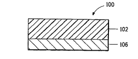
図1Aは、本発明の1つの実施形態による熱画像形成ドナー100の断面図である。熱画像形成ドナー100は、ベースフィルム102と、ベースフィルムの表面上に分散された新規な金属組成物を含む金属転写層106とを含む。
FIG. 1A is a cross-sectional view of a
ベースフィルム102は、熱画像形成ドナー100の他の層に対する支持を提供する。ベースフィルム102は、好ましくは透明であってLTHCまたは他の層の加熱にもかかわらず安定したままである可撓性ポリマーフィルムを含む。ベースフィルム102の適した厚さは約25μm〜約200μmであるが、より厚いまたはより薄い支持層を用いてもよい。ベースフィルムは、延伸フィルムおよびLTHC層などの1つまたは複数の他の層を製造するために本技術分野に公知の標準的プロセスによって延伸されてもよく、延伸プロセスの終了前にベースフィルム上にコートされてもよい。熱画像形成ドナーのための好ましいベースフィルムは、ポリエチレンテレフタレート(PET)、ポリエチレンナフタレート(PEN)、トリアセチルセルロースおよびポリイミドからなる群から選択されたポリマー材料を含む。
光減衰剤
光減衰剤が離散的な層に存在してもよく、またはベースフィルム、LTHC層などのドナー要素の他の機能層の1つにまたは付加的な転写層に導入されてもよい。1つの実施形態において、ベースフィルムは、熱画像形成工程の間にLTHC層中の放射線吸収剤上に放射線源を集束するのを助け、それによって熱伝達の効率を改良することができる染料などの光減衰剤の少量(典型的にベースフィルムの0.2質量%〜0.5質量%)を含む。本明細書において参照によって組み込まれた米国特許第6645681号明細書には、装置が画像形成レーザと非画像形成レーザとを含み、そこで非画像形成レーザが、画像形成レーザと連通している光検出器を有するレーザ放射線源の集束を助けるようにベースフィルムを改良することができるこの方法およびその他の方法が記載されている。本明細書において、光減衰剤は好ましくは、可視領域において光を吸収または拡散し、1つの実施形態において約670nmを吸収する。適した光減衰剤は本技術分野に公知であり、市販のディスパース・ブルー(Disperse Blue)60およびソルベント・グリーン(Solvent Green)28染料およびカーボンブラックなどが挙げられる。好ましくは光減衰剤の量は、約400〜約750nmの或る波長において0.1以上、より好ましくは約0.3〜約1.5の光学濃度(OD)を達成するのに十分である。
Light attenuating agent The light attenuating agent may be present in discrete layers or may be introduced into one of the other functional layers of the donor element, such as the base film, the LTHC layer, or in an additional transfer layer. In one embodiment, the base film helps to focus the radiation source onto the radiation absorber in the LTHC layer during the thermal imaging process, thereby improving the efficiency of heat transfer, such as a dye Contains a small amount of light attenuating agent (typically 0.2% to 0.5% by weight of the base film). U.S. Pat. No. 6,645,681, incorporated by reference herein, discloses that the apparatus includes an imaging laser and a non-imaging laser, where the non-imaging laser is in communication with the imaging laser. This and other methods have been described in which the base film can be modified to help focus the laser radiation source with the instrument. As used herein, the light attenuating agent preferably absorbs or diffuses light in the visible region, and in one embodiment absorbs about 670 nm. Suitable light attenuating agents are known in the art and include the commercially available Disperse
光−熱変換層(LTHC)
熱画像形成ドナーは、場合により、ベースフィルムと他の層との間に挟まれた、光−熱変換層(LTHC)を有してもよい。図1Bは、本発明の別の実施形態による熱画像形成ドナー100の断面図である。熱画像形成ドナー100は、ベースフィルム102と金属転写層106との間に挟まれたLTHC層108を含む。
Light-to-heat conversion layer (LTHC)
The thermal imaging donor may optionally have a light-to-heat conversion layer (LTHC) sandwiched between the base film and other layers. FIG. 1B is a cross-sectional view of a
LTHC層108は、発光源から放射された光のエネルギーを熱転写ドナーに結合するために放射線誘起熱転写のための熱画像形成ドナー100の一部として導入される。
The
典型的に、LTHC層(または他の層)中の放射線吸収剤は、電磁スペクトルの赤外線、可視線、および/または紫外線領域の光を吸収し、吸収された光を熱に変換する。放射線吸収剤は典型的に高吸収性であり、画像形成放射線の波長において0.1〜3以上、好ましくは0.2〜2の光学濃度(OD)を提供する。 Typically, the radiation absorber in the LTHC layer (or other layer) absorbs light in the infrared, visible, and / or ultraviolet region of the electromagnetic spectrum and converts the absorbed light into heat. The radiation absorber is typically highly absorptive and provides an optical density (OD) of from 0.1 to 3 and preferably from 0.2 to 2 at the wavelength of the imaging radiation.
適した放射線吸収材料には、例えば、染料(例えば、可視染料、紫外線染料、赤外線染料、螢光染料、および放射線偏光染料)、顔料、金属、金属化合物、金属フィルム、およびその他の適した吸収材料が挙げられる。LTHC層のための適した放射線吸収剤およびバインダーは本技術分野に公知であり、および詳細なリストおよび参考文献は、PCT/US05/38010号明細書、PCT/US05/38009号明細書、米国特許第6,228,555B1号明細書、マツオカ、M.(Matsuoka,M.)、「赤外線吸収材料(Infrared Absorbing Materials)」、プレナム・プレス(Plenum Press)、ニューヨーク(New York)、1990年、およびマツオカ、M.、「ダイオードレーザのための染料の吸収スペクトル(Absorption Spectra of Dyes for Diode Lasers)」、ブンシン出版社(Bunshin Publishing Co.)、東京(Tokyo)、1990年(その内容を参照によって本願明細書に組み入れる)に見出される。適したLTHC層の1つの実施例は、カーボンブラックなどの顔料、および有機ポリマーなどのバインダーを含有することができる。近赤外染料の好ましいクラスは、インドシアニン、多置換フタロシアニンおよび金属含有フタロシアニンなどのフタロシアニン、およびメロシアニンの群から選択されたシアニン化合物である。 Suitable radiation absorbing materials include, for example, dyes (eg, visible dyes, ultraviolet dyes, infrared dyes, fluorescent dyes, and radiation polarizing dyes), pigments, metals, metal compounds, metal films, and other suitable absorbing materials. Is mentioned. Suitable radiation absorbers and binders for the LTHC layer are known in the art, and a detailed list and references can be found in PCT / US05 / 38010, PCT / US05 / 38009, US patents. 6,228,555B1, Matsuoka, M .; (Matsuoka, M.), “Infrared Absorbing Materials”, Plenum Press, New York, 1990, and Matsuoka, M .; , "Absorption Spectra of Dies for Diode Lasers", Bunshin Publishing Co., Tokyo, 1990 (the contents of which are incorporated herein by reference). ). One example of a suitable LTHC layer can contain a pigment, such as carbon black, and a binder, such as an organic polymer. A preferred class of near-infrared dyes are cyanine compounds selected from the group of phthalocyanines, such as indocyanine, polysubstituted phthalocyanines and metal-containing phthalocyanines, and merocyanines.
適した赤外線吸収染料の供給元には、H.W.サンズ・コーポレーション(H.W.Sands Corporation)(米国、フロリダ州、ジュピター(Jupiter,FL,US))、アメリカン・シアナミッド・カンパニー(American Cyanamid Co.)(ニュージャージー州、ウェイン(Wayne,NJ))、サイテック・インダストリーズ(Cytec Industries)(ニュージャージー州、ウエストパターソン(West Paterson,NJ))、グレンデール・プロテクティブ・テクノロジー社(Glendale Protective Technologies,Inc.)(フロリダ州、レークランド(Lakeland,FL))およびハンプフォード・リサーチ社(Hampford Research Inc.)(コネチカット州、ストラットフォード(Stratford,CT))などがある。LTHCおよび転写層のための好ましい染料は、3H−インドリウム、2−[2−[2−クロロ−3−[(1,3−ジヒドロ−1,3,3−トリメチル−2H−インドル−2−イリデン)エチリデン]−1−シクロペンテン−1−イル]エテニル]−1,3,3−トリメチル−、コネチカット州、ストラトフォード、ハンプフォード・リサーチ社からTIC−5cとして入手可能な、1モル当たり約619グラムの分子量を有する、CASNo.[128433−68−1]のトリフルオロメタンスルホン酸との塩(1:1)の他、2−(2−(2−クロロ−3−(2−(1,3−ジヒドロ−1,1−ジメチル−3−(4−スルホブチル)−2H−ベンズ[e]インドル−2−イリデン)エチリデン)−1−シクロヘキセン−1−イル)エテニル)−1,1−ジメチル−3−(4−スルホブチル)−1H−ベンズ[e]インドリウム、H.W.サンズコーポレーション(H.W.Sands Corp)からSDA4927として入手可能なCASNo.[162411−28−1]の内部塩、遊離酸、およびH.W.サンズコーポレーション製のインドールニン染料SDA2860およびSDA4733である。SDA4927はLTHC層のための特に好ましい染料である。 Sources of suitable infrared absorbing dyes include H.I. W. Sands Corporation (HW Sands Corporation, Florida, USA, Jupiter, FL, US), American Cyanamid Co. (Wayne, NJ), Cytec Industries (West Paterson, NJ), Glendale Protective Technologies, Inc. (Lakeland, FL, and Lakeland, FL) Ford Research Inc. (Hampford Research Inc.) Nechikatto State, Stratford (Stratford, CT)), and the like. Preferred dyes for LTHC and transfer layer are 3H-indolium, 2- [2- [2-chloro-3-[(1,3-dihydro-1,3,3-trimethyl-2H-indole-2- Iridene) ethylidene] -1-cyclopenten-1-yl] ethenyl] -1,3,3-trimethyl-, available as TIC-5c from Hampford Research, Stratford, Conn., About 619 per mole CAS No. having a molecular weight of grams. In addition to the salt of [128433-68-1] with trifluoromethanesulfonic acid (1: 1), 2- (2- (2-chloro-3- (2- (1,3-dihydro-1,1-dimethyl) -3- (4-sulfobutyl) -2H-benz [e] indol-2-ylidene) ethylidene) -1-cyclohexen-1-yl) ethenyl) -1,1-dimethyl-3- (4-sulfobutyl) -1H Benz [e] indolium, H. W. CAS No. available as SDA4927 from HW Sands Corp. [162411-28-1] internal salts, free acids, and H.P. W. Indolenin dyes SDA2860 and SDA4733 manufactured by Sands Corporation. SDA 4927 is a particularly preferred dye for the LTHC layer.
LTHC層は、バインダー中の粒状放射線吸収剤を含有してもよい。適した顔料の例には、カーボンブラックおよび黒鉛がある。 The LTHC layer may contain a particulate radiation absorber in a binder. Examples of suitable pigments are carbon black and graphite.
質量パーセントの計算において溶剤を除いて、LTHC層中の放射線吸収剤の質量パーセントは概して、LTHC層中で使用された特定の放射線吸収剤およびバインダーに応じて、1質量%〜85質量%、好ましくは3質量%〜60質量%、最も好ましくは5質量%〜40質量%である。LTHC層において使用するための適したバインダーには、例えば、フェノール樹脂(例えば、ノボラックおよびレゾール樹脂)、ポリビニルブチラール樹脂、ポリビニルアセテート、ポリビニルアセタール、ポリ塩化ビニリデン、ポリアクリレート、およびスチレンアクリルなどのフィルム形成ポリマーがある。LTHC層の透過率の%は、放射線吸収剤の本性および量、およびLTHC層の厚さによって影響される。LTHC層は、熱転写画像形成プロセスにおいて使用された画像形成放射線の波長において、約20%〜約80%、より好ましくは約40%〜約50%の放射線透過率を示すのがよい。バインダーが存在するとき、放射線吸収剤の、バインダーに対する質量比は、約5:1〜約1:1000の質量比、好ましくは約2:1〜約1:100のの質量比である。ポリマーまたは有機LTHC層を0.05 m〜20 m、好ましくは、0.05 m〜10 m、より好ましくは、0.1 m〜5 mの厚さにコートする。 Excluding solvents in the weight percent calculation, the weight percent of radiation absorber in the LTHC layer is generally between 1% and 85% by weight, preferably depending on the specific radiation absorber and binder used in the LTHC layer. Is 3% to 60% by weight, most preferably 5% to 40% by weight. Suitable binders for use in the LTHC layer include film formation such as, for example, phenolic resins (eg, novolac and resole resins), polyvinyl butyral resins, polyvinyl acetate, polyvinyl acetal, polyvinylidene chloride, polyacrylate, and styrene acrylic. There is a polymer. The% transmission of the LTHC layer is affected by the nature and amount of radiation absorber and the thickness of the LTHC layer. The LTHC layer should exhibit a radiation transmission of about 20% to about 80%, more preferably about 40% to about 50%, at the wavelength of the imaging radiation used in the thermal transfer imaging process. When a binder is present, the mass ratio of radiation absorber to binder is from about 5: 1 to about 1: 1000, preferably from about 2: 1 to about 1: 100. The polymer or organic LTHC layer is coated to a thickness of 0.05 m to 20 m, preferably 0.05 m to 10 m, more preferably 0.1 m to 5 m.
本発明の好ましい実施形態において、LTHC層は、上に参照されたPCT/US05/38010号明細書およびPCT/US05/38009号明細書に開示されているような組成を有する多様な水溶性または水分散性ポリマーバインダーをベースとしている。好ましくは、その水性相中の水分散性バインダーの平均粒子径は0.1ミクロン未満、より好ましくは0.05ミクロン未満であり、好ましくは狭い粒度分布を有する。本発明において有用なLTHC層のための好ましい水溶性または水分散性ポリマーバインダーはアクリル樹脂、および親水性ポリエステルの群から、より好ましくは上に参照されたPCT/US05/38009号明細書において記載されたようなスルホン化ポリエステルから選択されたポリマーバインダーである。 In a preferred embodiment of the present invention, the LTHC layer has a variety of water soluble or water having compositions as disclosed in the above referenced PCT / US05 / 38010 and PCT / US05 / 38009 specifications. Based on dispersible polymer binder. Preferably, the average particle size of the water-dispersible binder in the aqueous phase is less than 0.1 microns, more preferably less than 0.05 microns, and preferably has a narrow particle size distribution. Preferred water-soluble or water-dispersible polymer binders for the LTHC layer useful in the present invention are described in the PCT / US05 / 38009 specification referenced above, more preferably from the group of acrylic resins and hydrophilic polyesters. A polymer binder selected from such sulfonated polyesters.
LTHC層のための他の好ましいポリマーバインダーは、無水マレイン酸ポリマーおよび/またはコポリマーをアルコール、アミン、およびアルカリ金属水酸化物で処理することによって提供された官能価を含むものを含めた無水マレイン酸ホモポリマーおよびコポリマーである。好ましい無水マレイン酸ベースのコポリマーは、式(III)

xおよびzが任意の正の整数であり、
yが0または任意の正の整数であり、
R21およびR22が同一または異なっていてもよく、R21およびR22の1つが芳香族基であることを条件として、個々に水素、アルキル、アリール、アラルキル、シクロアルキル、およびハロゲンであり、
R31、R32、R41およびR42が同一または異なった基であり、水素または1〜約5個の炭素原子のアルキルであってもよく、
R50が、
a)1〜約20個の炭素原子を含有するアルキル、アラルキル、アルキル置換アラルキル基、
b)1〜約20の反復単位を有しうる、各オキシアルキレン基中に約2〜約4個の炭素原子を含有するアルキル、アラルキル、アルキル置換アラルキル基のオキシアルキル化誘導体、
c)1〜約6の反復単位を有しうる、各オキシアルキレン基中に約2〜約4個の炭素原子を含有するアルキル、アラルキル、アルキル置換アラルキル基のオキシアルキル化誘導体、
d)少なくとも1つの不飽和部分、
e)少なくとも1つのヘテロ原子部分、
f)Li、Na、KおよびNH4 +から選択された塩を形成することができるアルカリ分子、および
g)それらの組合せ、から選択された官能基である。
Other preferred polymer binders for the LTHC layer are maleic anhydride, including those containing functionality provided by treating maleic anhydride polymers and / or copolymers with alcohols, amines, and alkali metal hydroxides. Homopolymers and copolymers. Preferred maleic anhydride based copolymers are of the formula (III)
x and z are any positive integers,
y is 0 or any positive integer;
R 21 and R 22 may be the same or different and are each independently hydrogen, alkyl, aryl, aralkyl, cycloalkyl, and halogen, provided that one of R 21 and R 22 is an aromatic group;
R 31 , R 32 , R 41 and R 42 are the same or different groups and may be hydrogen or alkyl of 1 to about 5 carbon atoms;
R 50 is
a) alkyl, aralkyl, alkyl-substituted aralkyl groups containing from 1 to about 20 carbon atoms,
b) alkyl, aralkyl, oxyalkylated derivatives of alkyl substituted aralkyl groups containing from about 2 to about 4 carbon atoms in each oxyalkylene group, which may have from 1 to about 20 repeating units;
c) alkyl, aralkyl, oxyalkylated derivatives of alkyl substituted aralkyl groups containing from about 2 to about 4 carbon atoms in each oxyalkylene group, which may have from 1 to about 6 repeating units;
d) at least one unsaturated moiety,
e) at least one heteroatom moiety;
f) an alkali molecule capable of forming a salt selected from Li, Na, K and NH 4 + , and g) a functional group selected from a combination thereof.
LTHC層のための好ましい無水マレイン酸ポリマーは、式(III)のコポリマーを含み、上式中、R21、R31、R32、R33、R41、R42、R43が個々に水素であり、R22がフェニルであり、R50が2−(n−ブトキシ)エチルである。LTHC層において有用な無水マレイン酸コポリマーの具体例は、ペンシルベニア州、エクストンのサートマー・コーポレーション(Sartomer Corporation,Exton,PA)の製品SMA1440Hなどのスチレン無水マレイン酸コポリマーである。 Preferred maleic anhydride polymers for the LTHC layer include copolymers of formula (III), wherein R 21 , R 31 , R 32 , R 33 , R 41 , R 42 , R 43 are each independently hydrogen. Yes, R 22 is phenyl and R 50 is 2- (n-butoxy) ethyl. A specific example of a maleic anhydride copolymer useful in the LTHC layer is a styrene maleic anhydride copolymer such as product SMA 1440H from Sartomer Corporation, Exton, Pa.
本発明の1つの実施形態において、好ましいLTHC層は、インドシアニン、多置換フタロシアニンおよび金属含有フタロシアニンなどのフタロシアニン、およびメロシアニンからなる群から選択された1つまたは複数の水溶性または水分散性放射線吸収性シアニン化合物と、アクリル樹脂、親水性ポリエステル、スルホン化ポリエステル、および無水マレイン酸ホモポリマーおよびコポリマーからなる群から選択された1つまたは複数の水溶性または水分散性ポリマーバインダーとを含む。 In one embodiment of the present invention, a preferred LTHC layer is one or more water soluble or water dispersible radiation absorbers selected from the group consisting of indocyanine, phthalocyanines such as polysubstituted phthalocyanines and metal-containing phthalocyanines, and merocyanines. And a water-soluble or water-dispersible polymer binder selected from the group consisting of acrylic resins, hydrophilic polyesters, sulfonated polyesters, and maleic anhydride homopolymers and copolymers.
最も好ましいLTHC層は、第四アンモニウムカチオン化合物、ホスフェートアニオン化合物、ホスホネートアニオン化合物、1〜5個のエステル基および2〜10個のヒドロキシル基を含む化合物、アルコキシル化アミン化合物、およびそれらの組合せからなる群から選択された1つまたは複数の剥離改質剤をさらに含む。 The most preferred LTHC layer consists of a quaternary ammonium cation compound, a phosphate anion compound, a phosphonate anion compound, a compound containing 1 to 5 ester groups and 2 to 10 hydroxyl groups, an alkoxylated amine compound, and combinations thereof Further comprising one or more release modifiers selected from the group.
また、参照によって本願明細書に組み入れられた米国特許第5,256,506号明細書に開示されているように、金属放射線吸収剤を粒子の形でまたはフィルムとしてLTHC層として用いてもよい。ニッケルおよびクロムはLTHC層108のための好ましい金属であり、クロムが特に好ましい。加熱層のためのいずれの他の適した金属も使用することができる。加熱層の好ましい厚さは、使用された金属の光吸収に依存する。クロム、ニッケル/バナジウム合金またはニッケルについては、80〜100オングストロームの層が好ましい。
Metal radiation absorbers may also be used as LTHC layers in the form of particles or as a film, as disclosed in US Pat. No. 5,256,506, incorporated herein by reference. Nickel and chromium are preferred metals for the
ここで利用されたLTHC層のための好ましい放射線吸収剤は、CrおよびNiから選択された金属フィルム、カーボンブラック、黒鉛、およびLTHC層中で約600〜1200nmの吸収極大を有する近赤外染料の群から選択される。 Preferred radiation absorbers for the LTHC layers utilized herein are metal films selected from Cr and Ni, carbon black, graphite, and near infrared dyes having an absorption maximum of about 600-1200 nm in the LTHC layer. Selected from the group.
付加的な転写層
図2Aは、本発明の別の実施形態による熱画像形成ドナー100の断面図である。熱画像形成ドナー100は、ベースフィルム102、付加的な転写層104、および層104の表面上に分散された金属転写層106を含む。
Additional Transfer Layer FIG. 2A is a cross-sectional view of a
図2Bは、本発明の別の実施形態による熱画像形成ドナー100の断面図である。熱画像形成ドナー100は、ベースフィルム102と付加的な転写層104との間に挟まれたLTHC層108、および付加的な転写層104上の金属転写層106を含む。
FIG. 2B is a cross-sectional view of a
熱画像形成ドナーは、金属転写層の下として本明細書において定義された、ベースフィルムと金属転写層との間に、または金属転写層の上として本明細書において定義された、ベースフィルムの反対側の金属転写層の側に配置された1つまたは複数の付加的な転写層を有してもよい。付加的な転写層の厚さは大体、約5nm〜約5μm、より好ましくは、約100nm〜約3μmでありうる。付加的な転写層は、例えば導電性、半導性、絶縁性、接着性、平坦化、光減衰または保護層として作用する機能層であってもよく、熱転写プロセスにおいて金属転写層と共に転写される。転写の後、付加的な転写層は、パターン化金属層の上にあってもよい。あるいは、付加的な転写層がドナーの金属層の上にある場合、転写の後、それは受容体と金属層との間にある。 The thermal imaging donor is defined herein as below the metal transfer layer, between the base film and the metal transfer layer, or opposite of the base film as defined herein as above the metal transfer layer. There may be one or more additional transfer layers disposed on the side of the side metal transfer layer. The thickness of the additional transfer layer can be approximately from about 5 nm to about 5 μm, more preferably from about 100 nm to about 3 μm. The additional transfer layer may be a functional layer that acts, for example, as a conductive, semiconductive, insulating, adhesive, planarizing, light attenuating or protective layer, and is transferred along with the metal transfer layer in a thermal transfer process. . After transfer, an additional transfer layer may be on the patterned metal layer. Alternatively, if an additional transfer layer is on the donor metal layer, after transfer, it is between the receptor and the metal layer.
導電層および抵抗層
様々な充填剤を有するかまたは有しないポリマーを含有する導体および抵抗層は、有用な付加的な転写層でありうる。有用な導電性層には、π共役有機ポリマーおよびこれらのポリマーのドープされた変種がある。好ましいポリマーは、以下のカテゴリーの1つまたは複数に属する。すなわち、(a)ポリアニリン(PANI)およびポリエチレンジオキシチオフェン(PEDOT)などの安定な導電性ポリマー、(b)PANI、PEDOTなど、標準コーティング技術を用いてフィルムを形成する可溶性または分散性導電性ポリマー、およびポリ(2,5ジアルコキシ)パラフェニレンビニレンおよびポリ(3−ヘキシル)チオフェンなどの導電性ポリマーのその他のアルキル−またはアルコキシ置換誘導体、および(c)ドープした時に高導電率をもたらす導電性ポリマー。本明細書において導電性ポリマーAと称される好ましい導電性ポリマーは、ポリアニリン、ポリチオフェン、ポリピロール、ポリへテロ芳香族ビニレン、およびそれらの誘導体からなる群から選択される。高導電性ポリマーおよび導電性ポリマーをドープするための方法の説明は、以下の参考文献、ブレダス,J.−L(Bredas,J.−L)、導電性ポリマーのハンドブック(Handbook of Conducting Polymers)、スコサイム,T.(Skotheim,T.)編、マーセル・デッカー社(Marcel Dekker,Inc.)、ニューヨーク、1986年、Vol.2、第25章、マクダーミッド,A.G.(MacDiarmid,A.G.)、Angew.Chem.Int.Ed.2001年、40、2581〜2590ページ、およびヘーガー,A.J.(Heeger,A.J.)、Angew.Chem.Int.Ed.2001年、40、2591〜2611ページに見出される。米国特許第5,863,465号明細書および米国特許第5,370,825号明細書には、ポリアニリンの導電性および半導性性質が記載されている。可塑化酸などの有機酸は好ましいドーパントである。さらに別の好ましいドーパントは、金、銀、銅、およびそれらの合金、ITO、ATO、カーボンナノチューブ、およびそれらの混合物からなる群から選択された導電性ナノ粒子である。
Conductive and Resistive Layers Conductors and resistive layers containing polymers with or without various fillers can be useful additional transfer layers. Useful conductive layers include π-conjugated organic polymers and doped variants of these polymers. Preferred polymers belong to one or more of the following categories: (A) stable conductive polymers such as polyaniline (PANI) and polyethylenedioxythiophene (PEDOT); (b) soluble or dispersible conductive polymers such as PANI and PEDOT that form films using standard coating techniques And other alkyl- or alkoxy-substituted derivatives of conductive polymers such as poly (2,5-dialkoxy) paraphenylene vinylene and poly (3-hexyl) thiophene, and (c) conductivity that provides high conductivity when doped polymer. The preferred conductive polymer referred to herein as conductive polymer A is selected from the group consisting of polyaniline, polythiophene, polypyrrole, polyheteroaromatic vinylene, and derivatives thereof. A description of highly conductive polymers and methods for doping conductive polymers can be found in the following references, Bredas, J. et al. -L (Bredas, J.-L), Handbook of Conducting Polymers, Scothym, T .; (Skotheim, T.), edited by Marcel Dekker, Inc., New York, 1986, Vol. 2, Chapter 25, McDermid, A.C. G. (MacDiarmid, AG), Angew. Chem. Int. Ed. 2001, 40, 2581-2590, and Hager, A .; J. et al. (Heeger, AJ), Angew. Chem. Int. Ed. 2001, 40, 2591-2611 pages. US Pat. No. 5,863,465 and US Pat. No. 5,370,825 describe the conductive and semiconductive properties of polyaniline. Organic acids such as plasticizing acids are preferred dopants. Yet another preferred dopant is a conductive nanoparticle selected from the group consisting of gold, silver, copper, and alloys thereof, ITO, ATO, carbon nanotubes, and mixtures thereof.
本発明の好ましい実施形態において、参照によって本願明細書に組み入れられた米国特許出願公開第2005/0116202号明細書に記載されているように、ポリアニリンおよびその誘導体の導電率を有機酸および場合によりカーボンナノチューブなどのドーパントで微調整して、導電率の適切なレベルを提供することができる。好ましい導電性の付加的な転写層は、単一壁カーボンナノチューブ(SWNT)、好ましくは約0.1〜12質量%のSWNTのポリアニリン分散体を含む。好ましくはポリアニリンおよびその誘導体はさらに、1〜30個の炭素を有する有機プロトン酸でドープされるが、この酸は、ポリマー主鎖中の窒素原子の約25%〜約100%のモル当量において存在する。好ましい有機プロトン酸はジノニルナフタレンスルホン酸(DNNSA)である。 In a preferred embodiment of the present invention, the conductivity of polyaniline and its derivatives is reduced to organic acids and optionally carbon, as described in US Patent Application Publication No. 2005/0116202, which is incorporated herein by reference. Fine tuning with dopants such as nanotubes can provide an appropriate level of conductivity. A preferred conductive additional transfer layer comprises a single-walled carbon nanotube (SWNT), preferably about 0.1 to 12% by weight of a polyaniline dispersion of SWNT. Preferably the polyaniline and its derivatives are further doped with an organic protic acid having 1 to 30 carbons, which acid is present in a molar equivalent of from about 25% to about 100% of the nitrogen atoms in the polymer backbone. To do. A preferred organic protonic acid is dinonylnaphthalene sulfonic acid (DNNSA).
付加的な転写層として有用な導体の好ましい厚さは、約0.01〜約10ミクロン、好ましくは約0.1〜約5ミクロン、より好ましくは約0.2〜約3ミクロンである。 The preferred thickness of the conductor useful as an additional transfer layer is from about 0.01 to about 10 microns, preferably from about 0.1 to about 5 microns, more preferably from about 0.2 to about 3 microns.
また、導電性の付加的な転写層は、導電性または抵抗性ナノ粒子でドープされた非導電性ポリマーを含有することができる。導電性の付加的な転写層を調合するのに有用な好ましい非導電性ポリマーは、アクリルおよびスチレン−アクリルラテックス、およびランダムおよびグラフトコポリマーを含めた溶液型アクリルおよびスチレン−アクリル(コ)ポリマーおよび(メタ)アクリレートコポリマー、およびそれらの組合せ、エチレンと(メタ)アクリレート、ビニルアセテート、一酸化炭素および(メタ)アクリル酸からなる群から選択された1つまたは複数のモノマーとのコポリマー、およびポリビニルアセテートおよびそのコポリマーからなる群から選択されると本明細書において定義された、非導電性ポリマーAである。非導電性ポリマーAの特に好ましい溶液型およびラテックスポリマーは、約−50℃〜約175℃、より好ましくは、約−30℃〜約90℃のTgを有する。この群の特に好ましい溶液型ポリマーは、約10,000〜約200,000のMwをさらに特徴とする。さらに、導電性の付加的な転写層を形成するのに有用な非導電性ポリマーBとして本明細書で称される好ましい非導電性ポリマーは、ポリビニルピロリドンおよびポリビニルピロリドン−コ−ビニルアセテートなどのそのコポリマーである。ドーパントとしての好ましい導電性ナノ粒子は、金、銀、銅、およびそれらの合金、ITO、ATO、カーボンナノチューブ、およびそれらの混合物からなる群から選択される。好ましいドーピングは、約40〜約90質量%のナノ粒子の範囲である。 The conductive additional transfer layer can also contain a non-conductive polymer doped with conductive or resistive nanoparticles. Preferred non-conductive polymers useful for formulating conductive additional transfer layers are solution-type acrylic and styrene-acrylic (co) polymers including acrylic and styrene-acrylic latex, and random and graft copolymers and ( (Meth) acrylate copolymers, and combinations thereof, copolymers of ethylene and one or more monomers selected from the group consisting of (meth) acrylates, vinyl acetate, carbon monoxide and (meth) acrylic acid, and polyvinyl acetate and Non-conductive polymer A as defined herein to be selected from the group consisting of the copolymers. Particularly preferred solution-type and latex polymers of non-conductive polymer A have a Tg of about -50 ° C to about 175 ° C, more preferably about -30 ° C to about 90 ° C. A particularly preferred solution-type polymer of this group is further characterized by a Mw of about 10,000 to about 200,000. In addition, preferred non-conductive polymers, referred to herein as non-conductive polymers B useful for forming conductive additional transfer layers, are those such as polyvinyl pyrrolidone and polyvinyl pyrrolidone-co-vinyl acetate. A copolymer. Preferred conductive nanoparticles as a dopant are selected from the group consisting of gold, silver, copper, and alloys thereof, ITO, ATO, carbon nanotubes, and mixtures thereof. Preferred doping ranges from about 40 to about 90% by weight nanoparticles.
誘電体層
顔料などの様々な充填剤を使用するかまたは使用しない絶縁ポリマーを含有する誘電体層は、本発明において有用な付加的な転写層でありうる。デバイスにおいて特に有用な誘電体層は、有機ポリマー、および高K誘電体ナノ粒子を配合されたポリマーを含有する。本明細書において高K誘電体ナノ粒子は、20以上、好ましくは30以上、より好ましくは100以上の誘電率を有するナノ粒子を指す。
Dielectric Layer A dielectric layer containing an insulating polymer with or without various fillers such as pigments can be an additional transfer layer useful in the present invention. Dielectric layers that are particularly useful in devices contain organic polymers and polymers formulated with high-K dielectric nanoparticles. As used herein, high-K dielectric nanoparticles refer to nanoparticles having a dielectric constant of 20 or more, preferably 30 or more, more preferably 100 or more.
本発明の1つの実施形態において、付加的な転写層104は、本明細書において層Aと称される、材料の少なくとも1つの層を含む約1014ohm−cm以上の抵抗率を有する誘電体層であって、アクリル、スチレンおよびスチレン−アクリルラテックス、溶液型アクリル、スチレンおよびスチレン−アクリルポリマー、およびそれらの組合せからなる群から選択されたアクリルおよびスチレンポリマー、部分水素化ポリ(4−ヒドロキシ)スチレン、ポリ(4−ヒドロキシ)スチレン、およびポリ(4−ヒドロキシ)スチレンとヒドロキシエチル(メタ)アクリレート、アルキル(メタ)アクリレート、スチレン、およびアルキル置換スチレン(アルキル基がC1〜C18直鎖または分岐鎖アルキル基である)とのコポリマーからなる群から選択されたヘテロ原子置換スチレンポリマー、フェノール−アルデヒド(コ)ポリマーおよび(コ)オリゴマーおよびそれらの組合せ、およびポリ(ビニルアセテート)からなる群から選択された1つまたは複数の誘電体ポリマーと、層A中に約600〜約1200nmの範囲の吸収極大を特徴とする1つまたは複数の近赤外染料を層Aの乾燥質量に基づいて約0.5質量%〜約10質量%とを含む誘電体層である。本明細書において誘電体ポリマーという用語は、ホモポリマー、2つ以上のモノマーの重合から誘導されたコポリマー、グラフト(コ)ポリマーなどの後誘導体化(コ)ポリマー、および低分子量ホモポリマーまたはコポリマーを包含する。ポリマーは直鎖、分岐状、超枝分かれまたはデンドリティックであってもよい。
In one embodiment of the invention, the
層Aのための好ましい誘電体ポリマーには、アルキル(メタ)アクリレート、スチレン、およびアルキル置換スチレン(アルキル基がC1〜C18直鎖または分岐鎖アルキル基である)を含むアクリル、スチレンおよびスチレン−アクリルラテックスがある。これらのラテックス系ポリマーのための好ましい任意のモノマーには、(メタ)アクリル酸、ヒドロキシエチル(メタ)アクリレートおよびグリシジル(メタ)アクリレートなどがある。より好ましいアクリル、スチレンおよびスチレン−アクリルラテックスは、アルキル(メタ)アクリレート、スチレン、およびアルキル置換スチレン(アルキル基がC1〜C18直鎖または分岐鎖アルキル基である)の群から選択されたモノマーを少なくとも約85質量%、好ましくは少なくとも約90質量%、より好ましくは少なくとも約95質量%含む1つまたは複数のラテックス樹脂として本明細書において定義されたラテックスAの群から選択される。これらのラテックス樹脂のための好ましい任意のモノマーには、好ましくは約5質量%までの(メタ)アクリル酸、好ましくは約10質量%までのヒドロキシエチル(メタ)アクリレート、および好ましくは約5質量%までのグリシジル(メタ)アクリレートが挙げられる。好ましくはラテックスは、平均粒子径が約150nm未満、より好ましくは、約100nm未満であり、酸価が約100未満、好ましくは約75未満、より好ましくは約25未満である。 Preferred dielectric polymers for layer A include acrylic (styrene) and styrene-acrylic, including alkyl (meth) acrylates, styrene, and alkyl-substituted styrenes (wherein the alkyl group is a C1-C18 linear or branched alkyl group). There is latex. Preferred optional monomers for these latex polymers include (meth) acrylic acid, hydroxyethyl (meth) acrylate and glycidyl (meth) acrylate. More preferred acrylic, styrene and styrene-acrylic latexes comprise at least monomers selected from the group of alkyl (meth) acrylates, styrene, and alkyl-substituted styrenes (wherein the alkyl group is a C1-C18 linear or branched alkyl group). Selected from the group of Latex A as defined herein as one or more latex resins comprising about 85% by weight, preferably at least about 90% by weight, more preferably at least about 95% by weight. Preferred optional monomers for these latex resins include preferably up to about 5% by weight (meth) acrylic acid, preferably up to about 10% by weight hydroxyethyl (meth) acrylate, and preferably about 5% by weight. Up to glycidyl (meth) acrylate. Preferably, the latex has an average particle size of less than about 150 nm, more preferably less than about 100 nm, and an acid number of less than about 100, preferably less than about 75, more preferably less than about 25.
高抵抗率(1014ohm−cmを超える)を有する層Aのための特に好ましいポリマーは、アクリルラテックスBおよびスチレン−アクリルラテックスCおよびそれらの組合せである。アクリルラテックスBは、メチルメタクリレートおよびブチルアクリレートからなる群から選択されたモノマーを少なくとも約85質量%、好ましくは少なくとも約90質量%、より好ましくは少なくとも約95質量%含む1つまたは複数のアクリルラテックスとして本明細書において定義されている。スチレン−アクリルラテックスCは、メチルメタクリレート、ブチルアクリレートおよびスチレンからなる群から選択されたモノマーの少なくとも約85質量%、好ましくは少なくとも約90質量%、より好ましくは少なくとも約95質量%を含む1つまたは複数のスチレン−アクリルラテックスとして本明細書において定義されている。アクリルラテックスBおよびスチレン−アクリルラテックスCのための好ましい任意のモノマーは、好ましくは約5質量%までの(メタ)アクリル酸、好ましくは約10質量%までのヒドロキシエチルメタクリレート、および好ましくは約5質量%までのグリシジルメタクリレートからなる群から選択される。誘電体ポリマーとして有用なアクリルおよびスチレンアクリルラテックスの商用の例には、ジョンクリル(Joncryl)(登録商標)95および1915(コ)ポリマー(ジョンソン・ポリマー(Johnson Polymer))がある。適したラテックスポリマーを合成するための方法は国際公開第03/099574号パンフレットに記載されている。 Particularly preferred polymers for layer A having high resistivity (greater than 10 14 ohm-cm) are acrylic latex B and styrene-acrylic latex C and combinations thereof. Acrylic latex B is one or more acrylic latexes containing at least about 85%, preferably at least about 90%, more preferably at least about 95% by weight of a monomer selected from the group consisting of methyl methacrylate and butyl acrylate. As defined herein. Styrene-acrylic latex C is one or more comprising at least about 85%, preferably at least about 90%, more preferably at least about 95% by weight of a monomer selected from the group consisting of methyl methacrylate, butyl acrylate and styrene. Multiple styrene-acrylic latexes are defined herein. Preferred optional monomers for acrylic latex B and styrene-acrylic latex C are preferably up to about 5% by weight (meth) acrylic acid, preferably up to about 10% by weight hydroxyethyl methacrylate, and preferably about 5% by weight. % Selected from the group consisting of up to% glycidyl methacrylate. Commercial examples of acrylic and styrene acrylic latexes useful as dielectric polymers include Joncryl® 95 and 1915 (co) polymers (Johnson Polymer). A method for synthesizing suitable latex polymers is described in WO 03/099574.
層Aのためのさらに別の好ましい誘電体ポリマーには、溶液型アクリル、スチレンおよびスチレン−アクリルポリマーがある。本明細書において用語「溶液型(solution−based)」は、水および/またはアルコール、例えばエタノールおよびブトキシエタノール、エーテル、例えばジメトキシエタン、エステル、例えば酢酸エチルおよび酢酸ブチル、ケトン、例えば、アセトンおよび2−ブタノン、および芳香族炭化水素、例えばキシレンなどの1つまたは複数の一般的な有機溶剤などの溶剤に可溶性である材料を指す。好ましい溶液型アクリル、スチレンおよびスチレン−アクリルポリマーは、約100,000未満、好ましくは約50,000未満、より好ましくは約30,000未満のMwを有する。さらに、好ましい溶液型アクリル、スチレンおよびスチレン−アクリルポリマーは、約250未満の酸価を有する。好ましい溶液型アクリル、スチレンおよびスチレン−アクリルポリマーは、アルキル(メタ)アクリレート、ベンジル(メタ)アクリレート、スチレン、およびアルキル置換スチレン(アルキル基がC1〜C18直鎖または分岐鎖アルキル基である)の群から選択されたモノマーを含む。これらの溶液型ポリマーのための好ましい任意のモノマーには、(メタ)アクリル酸およびヒドロキシエチル(メタ)アクリレートなどがある。 Still other preferred dielectric polymers for layer A include solution acrylic, styrene and styrene-acrylic polymers. As used herein, the term “solution-based” refers to water and / or alcohols such as ethanol and butoxyethanol, ethers such as dimethoxyethane, esters such as ethyl acetate and butyl acetate, ketones such as acetone and 2 -Refers to materials that are soluble in solvents such as butanone and aromatic hydrocarbons, such as one or more common organic solvents such as xylene. Preferred solution-type acrylic, styrene and styrene-acrylic polymers have a Mw of less than about 100,000, preferably less than about 50,000, more preferably less than about 30,000. Furthermore, preferred solution-type acrylic, styrene and styrene-acrylic polymers have an acid number of less than about 250. Preferred solution-type acrylic, styrene and styrene-acrylic polymers are the group of alkyl (meth) acrylates, benzyl (meth) acrylates, styrene, and alkyl-substituted styrenes (wherein the alkyl group is a C1-C18 linear or branched alkyl group). A monomer selected from Preferred optional monomers for these solution-type polymers include (meth) acrylic acid and hydroxyethyl (meth) acrylate.
層Aのための特に好ましい材料は、上に記載されたアクリル、スチレンおよびスチレン−アクリルラテックスと水性アクリル、スチレンおよびスチレン−アクリルポリマーとの配合物である。好ましくはこの配合物は、配合物の乾燥質量に基づいて、アクリルまたはスチレン−アクリルラテックス部分約20質量%〜約80質量%、より好ましくは約40質量%〜約80質量%および水性アクリルまたはスチレン−アクリルポリマー部分約20質量%〜約80質量%、より好ましくは約20質量%〜約60質量%を含む。 Particularly preferred materials for layer A are blends of the acrylic, styrene and styrene-acrylic latexes described above with aqueous acrylic, styrene and styrene-acrylic polymers. Preferably, the formulation is about 20% to about 80%, more preferably about 40% to about 80%, and aqueous acrylic or styrene based on the acrylic or styrene-acrylic latex portion, based on the dry weight of the formulation. -Contains about 20% to about 80%, more preferably about 20% to about 60% by weight of the acrylic polymer portion.
層Aのための他の好ましい誘電体ポリマーには、部分水素化ポリ(4−ヒドロキシ)スチレン、ポリ(4−ヒドロキシ)スチレン(PHS)、およびPHSとヒドロキシエチル(メタ)アクリレート、アルキル(メタ)アクリレート、スチレン、およびアルキル置換スチレン(アルキル基がC1〜C18直鎖または分岐鎖アルキル基である)とのコポリマーからなる群から選択されたヘテロ原子置換スチレンポリマーがある。特に好ましいコモノマーは、ヒドロキシエチルメタクリレート、ブチルアクリレート、メチルメタクリレートおよびスチレンであり、ヒドロキシエチルメタクリレートおよびブチルアクリレートが特に好ましい。PHS(コ)ポリマーは直鎖または分岐状であってもよい。PHSホモポリマーが使用されるとき、分岐状構造が好ましい。このクラスの好ましい(コ)ポリマーは、約30,000未満および好ましくは約20,000未満およびより好ましくは約10,000未満のMwを有する。部分水素化PHSは、ポリマー中の不飽和の約50当量%(equivalent %)まで水素化されているPHSポリマーを指し、好ましいポリマーは約10〜20当量%まで水素化されている。商用例には、PHS−B(分岐状PHSホモポリマー、テキサス州、ダラスのデュポン・エレクトロニック・テクノロジーズ(DuPont Electronic Technologies,Dallas,TX))、マルカ・リンカー(Maruka Lyncur)CMM(PHSとメチルメタクリレートとのコポリマー、日本、東京、丸善石油化学株式会社(Maruzen Petrochemical Co.,LTD.Tokyo))、マルカ・リンカーCHM(PHSとヒドロキシエチルメタクリレートとのコポリマー、丸善)、マルカ・リンカーCBA(PHSとブチルアクリレートとのコポリマー、丸善)、マルカ・リンカーCST15、50、および70(PHSとスチレンとのコポリマー、丸善)、およびマルカ・リンカーPHM−C(部分水素化PHS、丸善)などがある。 Other preferred dielectric polymers for layer A include partially hydrogenated poly (4-hydroxy) styrene, poly (4-hydroxy) styrene (PHS), and PHS and hydroxyethyl (meth) acrylate, alkyl (meth) There are heteroatom-substituted styrene polymers selected from the group consisting of copolymers with acrylates, styrene, and alkyl-substituted styrenes (wherein the alkyl group is a C1-C18 linear or branched alkyl group). Particularly preferred comonomers are hydroxyethyl methacrylate, butyl acrylate, methyl methacrylate and styrene, with hydroxyethyl methacrylate and butyl acrylate being particularly preferred. The PHS (co) polymer may be linear or branched. When a PHS homopolymer is used, a branched structure is preferred. Preferred (co) polymers of this class have a M w of less than about 30,000 and preferably less than about 20,000 and more preferably less than about 10,000. Partially hydrogenated PHS refers to a PHS polymer that has been hydrogenated to about 50 equivalent percent of the unsaturation in the polymer, with preferred polymers being hydrogenated to about 10 to 20 equivalent percent. Commercial examples include PHS-B (Branched PHS homopolymer, DuPont Electronic Technologies, Dallas, TX), Maruka Lyncur CMM (PHS and methyl methacrylate and Copolymer, Japan, Tokyo, Maruzen Petrochemical Co., LTD. Tokyo), Marka Linker CHM (copolymer of PHS and hydroxyethyl methacrylate, Maruzen), Marka Linker CBA (PHS and butyl acrylate) Copolymer, Maruzen), Marca Linker CST15, 50, and 70 (PHS and styrene copolymer, Maruzen), and Marca Lin Over PHM-C (partially hydrogenated PHS, Maruzen) and the like.
層Aのための他の好ましい誘電体ポリマーには、フェノール−アルデヒド(コ)ポリマー/(コ)オリゴマーおよびそれらの組合せからなる群から選択された誘電体ポリマーがある。このクラスの好ましい(コ)ポリマー/(コ)オリゴマーは、フェノール、アルキル−およびアリール置換フェノール、ホルムアルデヒド、およびアルキル−、アリール−およびヘテロ原子置換アルデヒドからなる群から選択されたモノ−およびビスフェノールおよびモノ−およびビスアルデヒドから誘導される。フェノール−アルデヒド樹脂をさらに誘導体化することができ、例えば、ヒドロキシ基をエーテル基に変換することができる。この群の好ましい(コ)ポリマー/(コ)オリゴマーは、約20,000以下、好ましくは約10,000以下のMwを有する。商用例には、ノボラック(Novolak)(登録商標)/ノボラック(登録商標)樹脂(ニューヨーク州、スケネクタディのスケネクタディ・インターナショナル社(Schenectady International Inc., Schenectady New York))がある。 Other preferred dielectric polymers for layer A include dielectric polymers selected from the group consisting of phenol-aldehyde (co) polymer / (co) oligomers and combinations thereof. Preferred (co) polymers / (co) oligomers of this class are mono- and bisphenols and mono selected from the group consisting of phenol, alkyl- and aryl-substituted phenols, formaldehyde, and alkyl-, aryl- and heteroatom-substituted aldehydes. Derived from-and bisaldehyde. Phenol-aldehyde resins can be further derivatized, for example, converting hydroxy groups to ether groups. Preferred (co) polymers / (co) oligomers of this group have a M w of about 20,000 or less, preferably about 10,000 or less. Commercial examples include Novolak (R) / Novolac (R) resin (Schenectady International Inc., Schenectady New York, Schenectady, NY).
層Aのための他の好ましい誘電体ポリマーには、ポリ(ビニルアセテート)ホモポリマーがある。この群の好ましいポリマーは約100,000以下のMwを有する。 Another preferred dielectric polymer for layer A is a poly (vinyl acetate) homopolymer. Preferred polymers in this group have a M w of about 100,000 or less.
上記のポリマーは、他の特性の中でもとりわけ、改良された可撓性、接着性、赤外線染料との相溶化のために可塑化されてもよい。特定の場合において、可塑剤は、ポリマーの上記のクラスから選択されてもよい。例えば、高めのTgまたは高めの分子量(MW)のフェノール−アルデヒドポリマーを低めのTgのまたは低めの分子量のフェノール−アルデヒドポリマーとブレンドすることができる。別の実施例は、フェノール−アルデヒドポリマーとブレンドされたPHSである。ポリマーの上記のクラスのいくつかのための適した可塑剤の例は、ポリ(エチレン)グリコール、グリセロールエトキシレート、ジ(エチレングリコール)ジベンゾエートの他、ジブチルフタレートなどのフタレート系可塑剤を含む。様々なポリマーのための多数の適している可能性のある可塑剤およびそれらの使用に関する詳細は、以下の文献:「可塑剤のハンドブック(Handbook of Plasticizers)」、G.ワイピク(G.Wypych)編、オンタリオ州、トロント(Toronto,Ont.)のケムテック・パブリッシング(ChemTec Publishing)、2004年に見出される。 The above polymers may be plasticized for improved flexibility, adhesion, compatibilization with infrared dyes, among other properties. In certain cases, the plasticizer may be selected from the above classes of polymers. For example, a higher Tg or higher molecular weight (MW) phenol-aldehyde polymer can be blended with a lower Tg or lower molecular weight phenol-aldehyde polymer. Another example is PHS blended with a phenol-aldehyde polymer. Examples of suitable plasticizers for some of the above classes of polymers include poly (ethylene) glycol, glycerol ethoxylate, di (ethylene glycol) dibenzoate, as well as phthalate plasticizers such as dibutyl phthalate. Details regarding a number of potentially suitable plasticizers for various polymers and their use can be found in the following document: "Handbook of Plasticizers", G.C. Found in 2004, ChemTec Publishing, Toronto, Ontario, edited by G. Wypych.
層Aは、層A中で約600〜約1200nmの範囲の吸収極大を特徴とする1つまたは複数の近赤外染料を層Aの乾燥質量に基づいて約0.5質量%〜約10質量%、より好ましくは約0.5質量%〜約6質量%含む。好ましくは近赤外染料は、その吸収バンドが転写プロセスにおいて使用された露光レーザの発光バンドと重なるように選択される。典型的に、露光レーザは、近赤外線範囲の放射線を放射する。染料の好ましいクラスは、インドシアニン、多置換フタロシアニンおよび金属含有フタロシアニンなどのフタロシアニン、およびメロシアニンの群から選択されたシアニン化合物である。近赤外染料の特に好ましいクラスは、約830nmにおいて吸収を有するインドシアニン染料のクラスである。830nm付近で吸収し、異なった溶剤および水への溶解性を有する多数の適したインドシアニン染料がH.W.サンズ・コーポレーションおよびその他の供給元から入手可能である。本発明の好ましい近赤外染料は、3H−インドリウム、2−[2−[2−クロロ−3−[(1,3−ジヒドロ−1,3,3−トリメチル−2H−インドル−2−イリデン)エチリデン]−1−シクロペンテン−1−イル]エテニル]−1,3,3−トリメチル−、CASNo.[128433−68−1]のトリフルオロメタンスルホン酸との塩(1:1)、2−(2−(2−クロロ−3−(2−(1,3−ジヒドロ−1,1−ジメチル−3−(4−スルホブチル)−2H−ベンズ[e]インドル−2−イリデン)エチリデン)−1−シクロヘキセン−1−イル)エテニル)−1,1−ジメチル−3−(4−スルホブチル)−1H−ベンズ[e]インドリウム、CASNo.[162411−28−1]の内部塩、遊離酸、および式(I)および(II)に相当するインドールニン染料およびそれらの共鳴構造の群から選択される。 Layer A contains from about 0.5% to about 10% by weight, based on the dry weight of Layer A, of one or more near-infrared dyes characterized by an absorption maximum in the range of about 600 to about 1200 nm. %, More preferably from about 0.5% to about 6% by weight. Preferably, the near-infrared dye is selected such that its absorption band overlaps with the emission band of the exposure laser used in the transfer process. Typically, the exposure laser emits radiation in the near infrared range. A preferred class of dyes are cyanine compounds selected from the group of phthalocyanines, such as indocyanine, polysubstituted phthalocyanines and metal-containing phthalocyanines, and merocyanines. A particularly preferred class of near-infrared dyes is that of indocyanine dyes that have an absorption at about 830 nm. A number of suitable indocyanine dyes that absorb near 830 nm and have solubility in different solvents and water are described in H.P. W. Available from Sands Corporation and other sources. Preferred near infrared dyes of the present invention are 3H-indolium, 2- [2- [2-chloro-3-[(1,3-dihydro-1,3,3-trimethyl-2H-indol-2-ylidene). ) Ethylidene] -1-cyclopenten-1-yl] ethenyl] -1,3,3-trimethyl-, CAS No. Salt of [128433-68-1] with trifluoromethanesulfonic acid (1: 1), 2- (2- (2-chloro-3- (2- (1,3-dihydro-1,1-dimethyl-3) -(4-Sulfobutyl) -2H-benz [e] indol-2-ylidene) ethylidene) -1-cyclohexen-1-yl) ethenyl) -1,1-dimethyl-3- (4-sulfobutyl) -1H-benz [E] Indolium, CAS No. Selected from the group of [162411-28-1] internal salts, free acids, and indolenin dyes corresponding to formulas (I) and (II) and their resonance structures.
材料中の好ましい染料レベルは、約0.2以上のフィルムの光学濃度をもたらし、約0.5〜約1.5の光学濃度が好ましい。好ましい光学濃度に達するために、無充填水性ラテックス系は典型的に、約4〜6質量%の高めの染料配合量を必要とする。無充填溶液型系は典型的に、約0.5〜約2質量%の低めの染料配合量を必要とする。 Preferred dye levels in the material result in an optical density of the film of about 0.2 or greater, with an optical density of about 0.5 to about 1.5 being preferred. To reach the desired optical density, unfilled aqueous latex systems typically require higher dye loadings of about 4-6% by weight. Unfilled solution type systems typically require lower dye loadings of about 0.5 to about 2% by weight.
別の好ましい実施形態において、誘電体層は、各勾配染料層が独立に約0.5〜約10質量%の近赤外染料の乾燥質量%を特徴とする勾配染料層である2つ以上の層Aを含み、そこで少なくとも1つの勾配染料層が近赤外染料の低めの質量%を有し、少なくとも1つの勾配染料層が近赤外染料の高めの質量%を有し、近赤外染料の高めの質量%が、近赤外染料の低めの質量%の質量%よりも少なくとも20%高い値である。 In another preferred embodiment, the dielectric layer is two or more gradient dye layers wherein each gradient dye layer is independently characterized by a dry weight percent of near infrared dye of from about 0.5 to about 10 weight percent. Layer A, wherein at least one gradient dye layer has a lower weight percent of near infrared dye and at least one gradient dye layer has a higher weight percent of near infrared dye, Is a value that is at least 20% higher than the lower mass% of the near infrared dye.
別の好ましい実施形態において、少なくとも1つの層Aは、層Aの乾燥質量に基づいて約10〜約90質量%の高κナノ粒子部分をさらに含み、ナノ粒子は、約20より大きい誘電率、および約5nm〜約500nmの平均粒子径を有する。本明細書において高κ誘電体ナノ粒子部分は、約20以上、好ましくは約30以上、より好ましくは約100以上の誘電率を有するナノ粒子を指す。この実施形態を実施するための好ましい誘電体ポリマーは、上述のように、アクリルおよびスチレン−アクリルラテックス、溶液型アクリルおよびスチレン−アクリル(コ)ポリマー、およびそれらの組合せ、およびフェノール−アルデヒド(コ)ポリマー/(コ)オリゴマーの群から選択される。この実施形態を実施するための好ましい高κ誘電体ナノ粒子は、チタン酸バリウム、チタン酸ストロンチウム、チタン酸バリウムストロンチウムおよび二酸化チタンの群から選択される。 In another preferred embodiment, the at least one layer A further comprises from about 10 to about 90% by weight of a high kappa nanoparticle portion based on the dry weight of layer A, the nanoparticles having a dielectric constant greater than about 20, And an average particle size of about 5 nm to about 500 nm. As used herein, a high κ dielectric nanoparticle portion refers to a nanoparticle having a dielectric constant of about 20 or more, preferably about 30 or more, more preferably about 100 or more. Preferred dielectric polymers for practicing this embodiment are acrylic and styrene-acrylic latex, solution acrylic and styrene-acrylic (co) polymers, and combinations thereof, and phenol-aldehyde (co), as described above. Selected from the group of polymers / (co) oligomers. Preferred high-κ dielectric nanoparticles for practicing this embodiment are selected from the group of barium titanate, strontium titanate, barium strontium titanate and titanium dioxide.
別の好ましい実施形態において、誘電体層は、各勾配ナノ粒子層が独立に約10〜約90質量%の高κ(高誘電率)ナノ粒子部分の乾燥質量%を特徴とする、勾配ナノ粒子層である2つ以上の層Aを含み、そこで少なくとも1つの勾配ナノ粒子層は、高κナノ粒子部分の低めの質量%を有し、少なくとも1つの勾配ナノ粒子層は、高κナノ粒子部分の高めの質量%を有し、高κナノ粒子部分の高めの質量%は低めの質量%の質量%よりも少なくとも20%高い値である。 In another preferred embodiment, the dielectric layer is a gradient nanoparticle wherein each gradient nanoparticle layer is characterized by a dry weight percent of high κ (high dielectric constant) nanoparticle portions that is independently about 10 to about 90 weight percent. Two or more layers A, wherein the at least one gradient nanoparticle layer has a lower mass% of the high κ nanoparticle portion, and the at least one gradient nanoparticle layer is a high κ nanoparticle portion The higher mass% of the high κ nanoparticle portion is at least 20% higher than the lower mass%.
別の好ましい実施形態において、誘電体層は、約1014ohm−cm以上の抵抗率を特徴とする、1つまたは複数の誘電体ポリマーを含む、本明細書において層Bと称される付加的な誘電体層をさらに含む。誘電体ポリマーの詳細なリストは、国際公開第03/052841号パンフレットおよび国際公開第06/024012号パンフレットに見出される。層Bのための好ましい誘電体ポリマーは、上記のように、アクリル、スチレンおよびスチレン−アクリルラテックス、溶液型アクリル、スチレンおよびスチレン−アクリルポリマー、およびそれらの組合せからなる群から選択されたアクリルおよびスチレンポリマー、部分水素化ポリ(4−ヒドロキシ)スチレン、ポリ(4−ヒドロキシ)スチレン、およびポリ(4−ヒドロキシ)スチレンとヒドロキシエチル(メタ)アクリレート、アルキル(メタ)アクリレート、スチレン、およびアルキル置換スチレン(アルキル基がC1〜C18直鎖または分岐鎖アルキル基である)とのコポリマーからなる群から選択されたヘテロ原子置換スチレンポリマー、フェノール−アルデヒド(コ)ポリマーおよび(コ)オリゴマーおよびそれらの組合せ、およびポリ(ビニルアセテート)からなる群から選択される。この実施形態はさらに、上に開示された他の実施形態を含めて実施することができる。層Bのための好ましい任意の添加剤には、カーボンブラックの他、チタン酸バリウム、チタン酸ストロンチウム、チタン酸バリウムストロンチウムおよび二酸化チタンからなる群から選択されたこの実施形態を実施するための好ましい高κ誘電体ナノ粒子を有する高κナノ粒子がある。 In another preferred embodiment, the dielectric layer comprises one or more dielectric polymers characterized by a resistivity of about 10 14 ohm-cm or greater, an additional layer referred to herein as layer B A dielectric layer. A detailed list of dielectric polymers can be found in WO 03/052841 and WO 06/024012. Preferred dielectric polymers for layer B are acrylic and styrene selected from the group consisting of acrylic, styrene and styrene-acrylic latex, solution acrylic, styrene and styrene-acrylic polymer, and combinations thereof, as described above. Polymers, partially hydrogenated poly (4-hydroxy) styrene, poly (4-hydroxy) styrene, and poly (4-hydroxy) styrene and hydroxyethyl (meth) acrylate, alkyl (meth) acrylate, styrene, and alkyl-substituted styrene ( Heteroatom-substituted styrene polymers, phenol-aldehyde (co) polymers and (co) oligomers and combinations thereof selected from the group consisting of copolymers with the alkyl group being a C1-C18 linear or branched alkyl group), And it is selected from the group consisting of poly (vinyl acetate). This embodiment can be further implemented, including the other embodiments disclosed above. Preferred optional additives for layer B include carbon black, as well as preferred high for carrying out this embodiment selected from the group consisting of barium titanate, strontium titanate, barium strontium titanate and titanium dioxide. There are high κ nanoparticles with κ dielectric nanoparticles.
別の好ましい実施形態において、付加的な転写層は、1014ohm−cm以上の抵抗率を有し、アクリル、スチレンおよびスチレン−アクリルラテックスからなる群から選択された1つまたは複数の誘電体ポリマーを含み、アルキル(メタ)アクリレート、スチレン、およびアルキル置換スチレン(アルキル基がC1〜C18直鎖または分岐鎖アルキル基である)からなる群から選択されたモノマーを少なくとも約85質量%含む、本明細書において層Cと称される、材料の少なくとも1つの層を含む。この実施形態はさらに、上に開示された他の実施形態を含めて実施することができる。1つの実施形態において層Cは、層Cの乾燥質量の約90質量%まで、高κナノ粒子部分をさらに含み、ナノ粒子部分は、約20より大きい誘電率、約5nm〜約500nmの平均粒子径を有する。層Cのための好ましい任意の添加剤には、カーボンブラックの他、チタン酸バリウム、チタン酸ストロンチウム、チタン酸バリウムストロンチウムおよび二酸化チタンからなる群から選択されたこの実施形態を実施するための好ましい高κ誘電体ナノ粒子を有する高κ誘電体ナノ粒子がある。 In another preferred embodiment, the additional transfer layer has one or more dielectric polymers selected from the group consisting of acrylic, styrene and styrene-acrylic latex having a resistivity of 10 14 ohm-cm or higher. And comprising at least about 85% by weight of a monomer selected from the group consisting of alkyl (meth) acrylates, styrene, and alkyl-substituted styrenes (wherein the alkyl group is a C1-C18 linear or branched alkyl group) Includes at least one layer of material, referred to as layer C in the text. This embodiment can be further implemented, including the other embodiments disclosed above. In one embodiment, layer C further comprises a high κ nanoparticle portion up to about 90% by weight of the dry weight of layer C, the nanoparticle portion having a dielectric constant greater than about 20, an average particle of about 5 nm to about 500 nm. Has a diameter. Preferred optional additives for layer C include carbon black as well as preferred high for carrying out this embodiment selected from the group consisting of barium titanate, strontium titanate, barium strontium titanate and titanium dioxide. There are high κ dielectric nanoparticles with κ dielectric nanoparticles.
層A、層Bおよび層Cにおいて利用された誘電体ポリマーのTgは、約−30〜約150℃、好ましくは約20〜約90℃および最も好ましくは約30〜約70℃の範囲である。典型的に、充填剤を添加することによって、より低いTgのポリマーの利用を可能にし、可塑剤を添加することによって、より高いTgのポリマーの利用を可能にする。誘電体層自体および層A、層B、および層Cなどの誘電体層中で利用された層の好ましいTgは、約30〜約100℃、好ましくは約40〜約85℃、最も好ましくは約45〜約65℃である。 The Tg of the dielectric polymer utilized in Layer A, Layer B and Layer C ranges from about -30 to about 150 ° C, preferably from about 20 to about 90 ° C and most preferably from about 30 to about 70 ° C. Typically, the addition of fillers allows the use of lower Tg polymers and the addition of plasticizers allows the use of higher Tg polymers. The preferred Tg of the dielectric layer itself and the layers utilized in dielectric layers such as Layer A, Layer B, and Layer C is from about 30 to about 100 ° C., preferably from about 40 to about 85 ° C., most preferably about 45 to about 65 ° C.
層A、任意の層Bおよび層Cは、充填剤、界面活性剤、脱泡剤、分散剤および粉砕助剤などの添加剤を含有してもよい。この目的のために適している多数の界面活性剤、脱泡剤、分散剤および粉砕助剤が入手可能である。選択はしばしば、観察されたコーティングおよび分散体の特質および熱転写プロセスにおいて他の層への誘電体層の所望の接着性に基づいている。特定の実施形態において、界面活性剤はシロキシ−、フルオリル−、アルキル−およびアルキニル置換界面活性剤を含む。これらには、バイク(Byk)(登録商標)(バイク・ケミー)、ゾニル(登録商標)(デュポン)、トリトン(登録商標)(ダウ)、サーフィノル(登録商標)(エア・プロダクツ)およびディノル(登録商標)(エア・プロダクツ)界面活性剤などがある。好ましいのは、バイク(登録商標)345、346および348およびゾニル(登録商標)FSOおよびFSN界面活性剤である。特定の実施形態において、脱泡剤は、アルキルおよびアルキニル官能価を含み、サーフィノル(登録商標)脱泡剤などが挙げられる。特定の実施形態において、分散剤は、官能化ポリマー、オリゴマーおよびモノマーを含み、サーフィノル(登録商標)およびディスパーバイク(Disperbyk)(登録商標)分散剤などが挙げられる。 Layer A, optional layer B and layer C may contain additives such as fillers, surfactants, defoamers, dispersants and grinding aids. A number of surfactants, defoamers, dispersants and grinding aids are available that are suitable for this purpose. The selection is often based on the observed coating and dispersion characteristics and the desired adhesion of the dielectric layer to other layers in the thermal transfer process. In certain embodiments, surfactants include siloxy-, fluoryl-, alkyl-, and alkynyl substituted surfactants. These include Byk (R) (Bike Chemie), Zonyl (R) (DuPont), Triton (R) (Dow), Surfinol (R) (Air Products) and Dinor (R) Trademark) (air products) surfactants. Preference is given to Bike® 345, 346 and 348 and Zonyl® FSO and FSN surfactants. In certain embodiments, the defoamer includes alkyl and alkynyl functionality, such as Surfinol® defoamer. In certain embodiments, dispersants include functionalized polymers, oligomers and monomers, such as Surfinol® and Disperbyk® dispersants.
誘電体層および層A、層Bおよび層Cなどの誘電体層中で利用された層の好ましい厚さは、約0.05〜約10ミクロン、好ましくは約0.1〜約5ミクロン、より好ましくは約0.2〜約3ミクロンである。 Preferred thicknesses of the dielectric layers and layers utilized in dielectric layers such as Layer A, Layer B and Layer C are from about 0.05 to about 10 microns, preferably from about 0.1 to about 5 microns, and more. Preferably it is about 0.2 to about 3 microns.
光吸収顔料を充填された誘電体ポリマーは、有用な付加的な転写層を製造する。このような層は、銀などの金属転写層の下または上で使用されるとき、特に有用である。この目的のための好ましい顔料はカーボンブラックである。好ましい組成物は約1質量%〜約90質量%のカーボンブラックである。 Dielectric polymers filled with light absorbing pigments produce useful additional transfer layers. Such a layer is particularly useful when used under or on a metal transfer layer such as silver. A preferred pigment for this purpose is carbon black. A preferred composition is about 1% to about 90% by weight carbon black.
熱画像形成ドナーの作製
金属転写層を含む熱画像形成ドナーを作製するために、金属組成物の分散液を熱画像形成基材の表面上に適用し、キャリア液を揮発させる。分散液の適用は、均一な層、または必要ならば、パターン化または不均一金属転写層を生じるどんな方法によって行なわれてもよい。ロッドコーティングおよびスピンコーティング、噴霧、印刷、ブレーディングまたはナイフ塗布(knifing)などのコーティングを使用することができる。コーティングおよび噴霧は、分散液を適用して均一な金属転写層を設けるための好ましい方法である。キャリア液は、蒸発させて金属転写層を設けることができ、または層は、熱および/または真空を適用するなどの乾燥のいずれかの従来の方法によって乾燥されてもよい。
Making a Thermal Imaging Donor To make a thermal imaging donor that includes a metal transfer layer, a dispersion of the metal composition is applied onto the surface of the thermal imaging substrate and the carrier liquid is volatilized. Application of the dispersion may be done by any method that produces a uniform layer, or if desired, a patterned or non-uniform metal transfer layer. Coatings such as rod coating and spin coating, spraying, printing, braiding or knife coating can be used. Coating and spraying are the preferred methods for applying the dispersion to provide a uniform metal transfer layer. The carrier liquid can be evaporated to provide a metal transfer layer, or the layer can be dried by any conventional method of drying, such as applying heat and / or vacuum.
熱画像形成ドナーは場合により、金属転写層の上または下に配置された1つまたは複数の付加的な転写層を含むことができる。図3Aは、本発明の別の実施形態による熱画像形成ドナー100の断面図である。熱画像形成ドナー100は、ベースフィルム102、金属転写層106および金属転写層の上の付加的な転写層110を含む。図3Bは、ベースフィルム102と金属転写層106との間に挟まれたLTHC層108をさらに備える関連の熱画像形成ドナー100の断面図である。図3Cは、関連熱画像形成ドナー100の断面図であり、そこで付加的な転写層104がLTHC層108と金属転写層106との間に挟まれ、付加的な転写層110が金属転写層の上にある。
The thermal imaging donor can optionally include one or more additional transfer layers disposed above or below the metal transfer layer. FIG. 3A is a cross-sectional view of a
本発明の特に好ましい実施形態は、光減衰層である付加的な転写層を備える。光減衰層を用いて最終電子デバイスの金属転写層の可視度を最小にすることができ、付加的な転写層として金属転写層のどちらかの側または両側の上に配置することができる。好ましくは光減衰層は、上に記載された好ましい誘電体材料および可視光線吸収染料または顔料から構成される。好ましい顔料はカーボンブラックである。 Particularly preferred embodiments of the present invention comprise an additional transfer layer that is a light attenuating layer. The light attenuating layer can be used to minimize the visibility of the metal transfer layer of the final electronic device and can be placed as an additional transfer layer on either or both sides of the metal transfer layer. Preferably the light attenuating layer is comprised of the preferred dielectric materials described above and a visible light absorbing dye or pigment. A preferred pigment is carbon black.
場合により、保護可剥性被覆シートが熱転写ドナーの最も外側の層上に存在してもよい。被覆シートは、下にある転写層を保護し、容易に除去可能である。 Optionally, a protective peelable cover sheet may be present on the outermost layer of the thermal transfer donor. The cover sheet protects the underlying transfer layer and can be easily removed.
熱画像形成受容体
図4は、受容体ベースフィルム202と任意の接着剤層204とを備える、本発明の1つの実施形態による熱画像形成受容体200の断面図である。受容体ベースフィルム202は、熱画像形成ドナーのベースフィルムのために画定されるような寸法安定シート材料である。さらに、受容体ベースフィルムは、二酸化チタンなどの白色顔料を充填されたポリエチレンテレフタレート、アイボリー紙、またはティヴェク(Tyvek)(登録商標)スパンボンドポリオレフィンなどの合成紙など、不透明な材料であってもよい。また、シート材料はガラスであってもよい。受容体のための好ましいベースフィルムはポリエチレンテレフタレート、ポリエチレンナフタレート、ポリイミド(カプトン(Kapton)(登録商標))およびガラスである。
Thermal Imaging Receptor FIG. 4 is a cross-sectional view of a
任意の接着剤層204は、熱画像形成された転写層への熱画像形成受容体200の接着性を促進する。適した接着剤層204は、付加的な転写層の説明において上に記載された(コ)ポリマー/コ(オリゴマー)/樹脂のいずれかを含む。ここで好ましい画像受容層は、上に定義されたようなアクリルラテックスAである。
The optional
パターン化多層組成物
上に定義された熱画像形成ドナーおよび受容体の様々な実施形態は、(a)1つまたは複数のベースフィルムと(b)1つまたは複数のパターン化金属層とを含む、同じく本発明のパターン化多層組成物を提供するのに有用であり、そこでパターン化金属層は、約1ミリメートル以下の幅の少なくとも1つのラインを含むパターンを有し、上に開示されたような金属組成物(A)を含む。好ましくはパターン化金属層は、少なくとも約200ミクロン以下の幅の少なくとも1つのラインを有する。他の実施形態において、パターン化金属層は、約150ミクロン以下、100ミクロン以下、50ミクロン以下、20ミクロン以下および10ミクロン以下の幅の少なくとも1つのラインを有する。好ましくは多層組成物は、約10−2ohm−cm以下および好ましくは約10−4ohm−cm以下の抵抗率を有する。
Patterned Multilayer Compositions Various embodiments of thermal imaging donors and receivers as defined above comprise (a) one or more base films and (b) one or more patterned metal layers. Also useful for providing the patterned multilayer composition of the present invention, wherein the patterned metal layer has a pattern comprising at least one line having a width of about 1 millimeter or less, as disclosed above. Metal composition (A). Preferably, the patterned metal layer has at least one line having a width of at least about 200 microns or less. In other embodiments, the patterned metal layer has at least one line that is about 150 microns or less, 100 microns or less, 50 microns or less, 20 microns or less, and 10 microns or less in width. Preferably, the multilayer composition has a resistivity of about 10 −2 ohm-cm or less and preferably about 10 −4 ohm-cm or less.
パターン化多層組成物はさらに、パターン化金属層の下として本明細書において定義された、ベースフィルムとパターン化金属層との間に、またはパターン化金属層の上として本明細書において定義された、ベースフィルムの反対側のパターン化金属フィルムの側に配置された付加的なパターン化層を含有することができる。付加的なパターン化層、およびそれらの好ましい実施形態は、付加的な転写層のために有用かつ好ましいとして上に開示されたそれらの材料および層に相当する。 The patterned multilayer composition is further defined herein as below the patterned metal layer, between the base film and the patterned metal layer, or above the patterned metal layer. It may contain an additional patterned layer disposed on the side of the patterned metal film opposite the base film. Additional patterned layers, and their preferred embodiments, correspond to those materials and layers disclosed above as useful and preferred for additional transfer layers.
パターン化多層組成物は、薄膜トランジスタ、ディスプレイ、およびタッチパッドなどの電子デバイスのための電子回路として有用である。好ましい適用においてパターン化多層組成物は、外側の放射線から電子デバイスを遮蔽し、デバイスから放射する放射線から局部環境を遮蔽するために用いられてもよい電磁干渉(EMI)シールドとして有用である。デバイスの典型的な実施例は、多量の電磁放射線を発生するプラズマディスプレイパネル(PDP)である。通常、フロントパネルは、電磁放射線を遮蔽するためにPDPの前に配置される。フロントパネルは、ディスプレイのスクリーンから放射された電磁放射線を遮蔽するために30MHz〜約1GHzの範囲において30デシベル(dB)以上の遮蔽機能を有しなければならない。これは通常、透明なベースフィルム上に取り付けられた金属メッシュの非常に薄いパターンによって達成される。EMIシールドの金属メッシュ(ライン)は、可視度を低下させないのがよく、適切な透明性を有するのがよい。典型的に金属メッシュは、例えば、米国特許出願公開第2006/0088690A1号明細書に記載されているように、フォトリソグラフィ工程によって設けられる。 The patterned multilayer composition is useful as an electronic circuit for electronic devices such as thin film transistors, displays, and touch pads. In preferred applications, the patterned multilayer composition is useful as an electromagnetic interference (EMI) shield that may be used to shield electronic devices from outside radiation and shield the local environment from radiation emanating from the device. A typical example of a device is a plasma display panel (PDP) that generates a large amount of electromagnetic radiation. Usually, the front panel is placed in front of the PDP to shield electromagnetic radiation. The front panel must have a shielding function of 30 decibels (dB) or higher in the range of 30 MHz to about 1 GHz to shield electromagnetic radiation emitted from the display screen. This is usually achieved by a very thin pattern of metal mesh mounted on a transparent base film. The metal mesh (line) of the EMI shield should not degrade visibility and should have appropriate transparency. Typically, the metal mesh is provided by a photolithographic process, for example, as described in US 2006/0088690 A1.
EMIシールドにおいて有用なベースフィルムには、ガラスまたはアクリルもしくはポリカーボネートなどの透明なポリマーなど、透明な無機化合物が挙げられる。具体例には、PET、ポリスルホン、ポリエーテルスルホン、ポリスチレン、ポリエチレンナフタレート、ポリアクリレート、ポリエーテルケトン、ポリカーボネート、ポリプロピレン、ポリメチルメタクリレートなどがある。本発明のEMIシールドのための好ましいベースフィルムは、ポリエチレンテレフタレート、ポリエチレンナフタレート、トリアセチルセルロースおよびガラスからなる群から選択される。 Base films useful in EMI shielding include transparent inorganic compounds such as glass or transparent polymers such as acrylic or polycarbonate. Specific examples include PET, polysulfone, polyethersulfone, polystyrene, polyethylene naphthalate, polyacrylate, polyetherketone, polycarbonate, polypropylene, polymethylmethacrylate, and the like. A preferred base film for the EMI shield of the present invention is selected from the group consisting of polyethylene terephthalate, polyethylene naphthalate, triacetyl cellulose and glass.
本発明の別の実施形態は、パターン化金属層の下、またはパターン化金属層の上に配置された付加的なパターン化層をさらに含む、上述の電磁シールドである。好ましくはこの付加的なパターン化層は、光減衰層であり、最も好ましくは付加的なパターン化層は約1〜約90質量%のカーボンブラックを含む。 Another embodiment of the present invention is an electromagnetic shield as described above, further comprising an additional patterned layer disposed below or over the patterned metal layer. Preferably the additional patterned layer is a light attenuating layer, and most preferably the additional patterned layer comprises from about 1 to about 90% by weight carbon black.
好ましくはEMIシールドは、ベースフィルムの表示側の表面上に反射防止層をさらに含む。反射防止フィルムは概して、光学レンズ、陰極線管ディスプレイデバイス(CRT)、プラズマディスプレイパネル(PDP)、液晶ディスプレイデバイス(LCD)、または有機エレクトロルミネセントデバイスなどの画像ディスプレイデバイスの最も外側の表面上に配置され、外部の光からの光学干渉を防ぐために反射率を低減させる。様々な市販の単一層および多層反射防止フィルムがある。多層反射防止フィルムは、交互の高回折および低回折層から構成される。適した高回折層は、酸化ニオブ、酸化チタン、酸化ジルコニウムおよびITOの層である。適した低回折層は、酸化ケイ素、フッ化マグネシウムなどの層である。反射防止フィルムには、拡散反射モードで外部の光を反射する微細に粗面化された表面を有する層を有するものがある。反射防止材料およびコーティングに関する一般的な参考文献については、ドブロボルスキJ.A.(Dobrowolski,J.A.)「光学素子のハンドブック(Handbook of Optics)」、バス,M.(Bass,M.)編、マグローヒル社(McGraw−Hill,Inc.)、ニューヨーク、1995年、Vol.1、第42章を参照のこと。 Preferably, the EMI shield further includes an antireflection layer on the display side surface of the base film. The antireflective film is generally disposed on the outermost surface of an image display device such as an optical lens, cathode ray tube display device (CRT), plasma display panel (PDP), liquid crystal display device (LCD), or organic electroluminescent device. The reflectance is reduced to prevent optical interference from external light. There are a variety of commercially available single layer and multilayer antireflective films. The multilayer antireflective film is composed of alternating high and low diffractive layers. Suitable high diffractive layers are niobium oxide, titanium oxide, zirconium oxide and ITO layers. Suitable low diffraction layers are layers of silicon oxide, magnesium fluoride and the like. Some antireflection films have a layer having a finely roughened surface that reflects external light in a diffuse reflection mode. For general references on antireflective materials and coatings, see Dobroborski J. et al. A. (Dobrowolski, JA) "Handbook of Optics", Bus, M.C. (Bass, M.), McGraw-Hill, Inc., New York, 1995, Vol. 1. See Chapter 42.
本発明の別の実施形態は、上述のようなパターン化金属層を有する多層組成物を含むタッチパッドセンサである。好ましくはタッチパッドセンサは、上の「誘電体層」と題された節に開示されているような誘電体層を含む。1つの実施形態においてタッチパッドセンサは、第1のパターン化金属層を有する第1のベースフィルムと、第2のパターン化金属層を有する第2のベースフィルムと、第1のパターン化金属層と第2のパターン化金属層との間に配置された誘電体層とを含む。別の実施形態においてタッチパッドセンサは、2つの対向した表面を有する第1のベースフィルムと、2つの対向した表面の各々の上に配置されたパターン化金属層と、パターン化金属層の各々の上の誘電体層とを含む。 Another embodiment of the present invention is a touchpad sensor comprising a multilayer composition having a patterned metal layer as described above. Preferably, the touchpad sensor includes a dielectric layer as disclosed in the section entitled “Dielectric Layer” above. In one embodiment, the touchpad sensor includes a first base film having a first patterned metal layer, a second base film having a second patterned metal layer, and a first patterned metal layer. And a dielectric layer disposed between the second patterned metal layer. In another embodiment, the touchpad sensor includes a first base film having two opposing surfaces, a patterned metal layer disposed on each of the two opposing surfaces, and each of the patterned metal layers. And an upper dielectric layer.
パターン化多層組成物を提供するための熱転写
パターン化多層組成物を提供するために熱画像形成ドナーは、熱画像形成受容体と接触される。接触されるとは、ドナーが、受容体によく近接している、好ましくは数ミクロンの範囲内であることを意味する。受容体は、例えば、ドナーと受容体との間に制御された間隙を設けるためのスペーサとして作用する予め印刷された層、ファイバーまたは粒子によってドナーからずらされてもよい。真空および/または圧力を用いて、ドナー要素100と受容体要素200とを一緒に保持することができる。1つの選択肢として、ドナー要素100と受容体要素200とを、接合体の外面において層を融着することによって一緒に保持することができる。
Thermal transfer to provide a patterned multilayer composition A thermal imaging donor is contacted with a thermal imaging receiver to provide a patterned multilayer composition. Contacted means that the donor is in close proximity to the receptor, preferably in the range of a few microns. The receptor may be offset from the donor by, for example, a preprinted layer, fiber or particle that acts as a spacer to provide a controlled gap between the donor and the receptor. Vacuum and / or pressure can be used to hold
金属転写層の少なくとも一部分、および場合により1つまたは複数の付加的な転写層の一部分を熱転写によって熱画像形成受容体に転写してパターン化金属層を形成する。熱転写をレーザ媒介転写プロセスによって行なうことができる。1つの実施形態において、ドナー要素100と受容体要素200との接合体を熱に選択的に暴露するが、それは、基材上に形成される所望のパターンの画像の露光パターンにおいてのレーザ放射線の形態であるのが好ましい。転写されるそれらの層とドナーを有している層との間の境界面に周りにレーザ放射線を集束させる。例えば、LTHC層が存在する場合、LTHC層と金属層との間の境界面上にレーザを集束させる。十分な放射線を適用して受容体への所望の転写層の転写を行なう。
At least a portion of the metal transfer layer, and optionally a portion of one or more additional transfer layers, is transferred by thermal transfer to a thermal imaging receiver to form a patterned metal layer. Thermal transfer can be performed by a laser-mediated transfer process. In one embodiment, the conjugate of the
様々な発光源を用いて熱転写ドナー要素を加熱することができる。アナログ技術(例えば、マスクを通しての露光)については、強力光源(例えば、キセノン閃光ランプおよびレーザ)が有用である。デジタル画像形成技術については、赤外線、可視線、および紫外線レーザが特に有用である。他の光源および照射条件が、とりわけ、ドナー要素の構成、転写層材料、熱転写の方式、およびその他のかかる要因に基づいて適していることがある。 A variety of light emitting sources can be used to heat the thermal transfer donor element. For analog techniques (eg, exposure through a mask), powerful light sources (eg, xenon flash lamps and lasers) are useful. For digital imaging techniques, infrared, visible and ultraviolet lasers are particularly useful. Other light sources and irradiation conditions may be suitable based on, among other things, the configuration of the donor element, the transfer layer material, the mode of thermal transfer, and other such factors.
放射線は好ましくは、ベースフィルム102の裏側、すなわち、金属転写層を含有しない側を通して適用される。レーザ放射線は好ましくは、約600mJ/cm2まで、より好ましくは約75〜440mJ/cm2までのレーザフルエンスにおいて提供される。様々なタイプのレーザを使用することができる。レーザは赤外線、近赤外線または可視領域において放射するのが好ましい。特に有利であるのは、それらの小さなサイズ、低コスト、安定性、信頼性、丈夫さおよび変調(modulation)の容易さの点からかなりの利点をもたらす750〜870nmの領域において放射するダイオードレーザである。780〜850nmの範囲で放射するダイオードレーザが最も好ましい。このようなレーザは、例えば、スペクトラ・ダイオード・ラボラトリーズ(Spectra Diode Laboratories)(カリフォルニア州、サンノゼ(San Jose,CA))から入手可能である。他のタイプのレーザおよび他の波長バンドを放射するレーザも同様に使用してもよい。画像を受容体に適用するために使用された1つのデバイスは、830nm付近で放射するレーザを利用する、クレオ・スペクトラム・トレンドセッター(Creo Spectrum Trendsetter)3244Fである。このデバイスは、約830nmレーザダイオードアレイからの5〜50ワットの出力を分割および変調する空間光変調器を利用する。対応する光学素子は、この光を画像形成可能な要素上に集束する。これは、約10×10〜2×10ミクロンのスポットに10〜200mWの光を各々有する、50〜240の単一ビームのアレイに集束された、ドナー要素上の0.1〜30ワットの画像形成光を生じる。同様な露光は、米国特許第4,743,091号明細書に開示されているような、1スポットに対して単一レーザを用いて得られる。この場合、各レーザは、780〜870nmにおいて50〜300mWの電気的に変調された光を放射する。他の選択肢には、各々が個々に変調され媒体上に集束された500〜3000mWを放射するファイバー結合レーザがある。このようなレーザは、アリゾナ州、ツーソン(Tucson,AZ)のオプト・パワー(Opto Power)から入手することができる。
The radiation is preferably applied through the back side of the
露光した後、ドナー要素100と受容体要素200とが図5Aおよび5Bに示されるように分離され、金属転写層106の転写されない部分をドナー要素100上に残し、パターン化金属転写層106を受容体要素200上に残す。図6Aおよび6Bは、付加的な転写層104が金属転写層と共に受容体200に転写される実施形態を示す。図7は、ベースフィルム202と少なくとも1つのパターン化層205とを含む別の熱画像形成受容体200の断面図である。パターン化層205は、パターン化半導体層、パターン化導体層およびパターン化誘電体層からなる群から選択されうる。
After exposure,
パターン化多層組成物は、使用済みドナー要素(画像の雌型)、画像形成された受容体要素(画像の雄型)、または両方の要素によって提供することができる。さらに、使用済みドナー要素および画像形成された受容体要素のどちらかまたは両方が、永久基材として利用されてもよく、または画像は、使用済みドナーまたは受容体から好ましくは積層によって永久基材に転写されてもよい。 The patterned multilayer composition can be provided by a used donor element (image female), an imaged receiver element (image male), or both elements. In addition, either or both of the used donor element and the imaged receiver element may be utilized as a permanent substrate, or the image is transferred from the used donor or receptor to the permanent substrate, preferably by lamination. It may be transcribed.
通常、転写層の転写された部分は、レーザ放射線に露光された転写層のそれらの部分に相当する。いくつかの場合では、ドナー要素100と受容体要素200とが分離されるとき、ドナーおよび受容体要素の性質および転写加工パラメータに依存して、受容体要素は、1つまたは複数の転写層の露光された部分と露光されていない部分との両方を備える。熱画像形成受容体の表面上に1つまたは複数の熱転写層の露光された部分と露光されていない部分とを含む熱画像形成受容体上のパターンの解像度を強化するための方法は、(a)熱画像形成受容体の前記表面を接着剤表面と接触させて仮積層体を提供する工程と、(b)前記接着剤表面を仮積層体から除去して、1つまたは複数の転写層の前記露光されていない部分を実質的に含有しない表面を有する熱画像形成受容体を提供する工程とを含む。この方法を実施するための適した接着剤表面は市販の接着テープであり、例えば、3M社(3M company)から入手可能なそれらのスコッチ(Scotch)(登録商標)ブランド・テープである。粘着ローラー、例えば、SDI(カリフォルニア州、アーバイン、システムズ・デヴィジョン社(Systems Division,Inc.)92618−2005)からダスト・リムーバル・システム(Dust Removal System)−1(レッド)の形で入手可能な中粘着ローラーは、この方法のために適した接着剤表面である。また、上に記載されたLTHC層として使用されたクロムフィルムは、非常にゆるい条件下で転写層の露光されていない部分を除去するための有用な低粘着接着剤層を製造する。
Usually, the transferred portions of the transfer layer correspond to those portions of the transfer layer that have been exposed to laser radiation. In some cases, when the
少なくとも一部は、本発明の使用によって形成されうる様々な電気的要素には、電子回路部品、レジスタ、キャパシタ、ダイオード、整流器、エレクトロルミネセンスランプ、メモリ要素、電界効果トランジスタ、二極トランジスタ、単接トランジスタ、薄膜トランジスタ、金属−絶縁体−半導体スタック、有機トランジスタ、電荷結合デバイス、絶縁体−金属−絶縁体スタック、有機導体−金属−有機導体スタック、集積回路、光検出器、レーザ、レンズ、導波路、格子、ホログラフィック素子、フィルター(例えば、アッド・ドロップ・フィルター(add−drop filters)、ゲイン・フラットニング・フィルター(gain−flattening filters)、カットオフフィルター等)、スプリッタ、カプラー、コンバイナ、変調器、センサ(例えば、エバネッセントセンサ、位相変調センサ、干渉応用センサ等)、光共振器、圧電(piezo−electric)デバイス、強誘電(ferroelectric)デバイス、薄膜バッテリ、またはそれらの組合せ、例えば、光ディスプレイのためのアクティブマトリクスアレイとして電界効果トランジスタと有機エレクトロルミネセンスランプとの組合せなどがある。 Various electrical elements that can be formed, at least in part, by use of the present invention include electronic circuit components, resistors, capacitors, diodes, rectifiers, electroluminescent lamps, memory elements, field effect transistors, bipolar transistors, Contact transistor, thin film transistor, metal-insulator-semiconductor stack, organic transistor, charge-coupled device, insulator-metal-insulator stack, organic conductor-metal-organic conductor stack, integrated circuit, photodetector, laser, lens, conductor Waveguides, gratings, holographic elements, filters (eg, add-drop filters, gain-flattening filters, cut-off filters, etc.), splitters, couplers, Combiner, modulator, sensor (eg, evanescent sensor, phase modulation sensor, interference applied sensor, etc.), optical resonator, piezoelectric-electric device, ferroelectric device, thin film battery, or combinations thereof, eg An active matrix array for an optical display includes a combination of a field effect transistor and an organic electroluminescent lamp.
材料
特に記載しない限り、化学物質はさらに精製せずに受け入れられたまま使用した。ポリマー、可塑剤、赤外線染料、および界面活性剤は、本明細書に記載された供給元から入手されたかまたはアルドリッチ(Aldrich)から購入された。カーボンブラック分散体などの顔料はペンシルベニア州、ドイルスタウン、ペン・カラー社(Penn Color,Inc.,Doylestown,PA)から入手された。銀ナノ粒子は、フェロー・カンパニー(Ferro Co.)−エレクトロニック・マテリアル・システムズ(Electronic Material Systems)、ナノストラクチャード・アンド・アモルファス・マテリアルズ社(Nanostructured & Amorphous Materials, Inc.)および三井株式会社(Mitsui Co.)から購入された。HiPco原料CNtは、テキサス州、ヒューストンのカーボンナノテクノロジー社(Carbon Nanotechnologies,Inc.,Houston TX)から購入された。
Materials Unless otherwise noted, chemicals were used as received without further purification. Polymers, plasticizers, infrared dyes, and surfactants were obtained from the suppliers described herein or purchased from Aldrich. Pigments such as carbon black dispersions were obtained from Penn Color, Inc., Doyletown, Pa., Doylestown, Pennsylvania. Silver nanoparticles are available from Ferro Co.-Electronic Material Systems, Nanostructured & Amorphous Materials, Inc. and Mitsui Corporation (Mitsui, Inc.). Co.). HiPco raw material CNt was purchased from Carbon Nanotechnology, Inc., Houston TX, Houston, Texas.
ドナー基材
Cr LTHC層。ポリエチレンテレフタレートのベースフィルム(PET、特に記載しない限り全ての実施例において厚さ50ミクロン)をヴァージニア州、マーティンスヴィル(Martinsville,VA.)のCPフィルムによって真空蒸着チャンバ内でクロム金属でコートした。光減衰剤(670nmの吸収剤)を用いておよび用いずにPETフィルム上で金属化を行なった。50%Tおよび40%Tの両方でクロム層をコートした。実施例において、これらのドナーフィルムは、光減衰剤を用いない金属化フィルムについて、40%T Cr PETドナー基材および50%T Cr PETドナー基材と称される。670nmの吸収剤がベースフィルムに導入されたドナーフィルムは、40%T CrブルーPETドナー基材および50%T CrブルーPETドナー基材と称される。
Donor substrate Cr LTHC layer. A polyethylene terephthalate base film (PET, 50 microns thick in all examples unless otherwise noted) was coated with chromium metal in a vacuum deposition chamber by a CP film from Martinsville, Va. Metallization was performed on PET film with and without light attenuating agent (670 nm absorber). The chromium layer was coated with both 50% T and 40% T. In the examples, these donor films are referred to as 40% T Cr PET donor substrate and 50% T Cr PET donor substrate for metallized films that do not use a light attenuating agent. Donor films with 670 nm absorber introduced into the base film are referred to as 40% T Cr blue PET donor substrate and 50% T Cr blue PET donor substrate.
有機LTHC層。有機LTHC層を上で参照したPCT/US05/38009号明細書の実施例の調合物Lにおいて記載されているように作製した。
LTHCコーティング調合物を以下の材料から調製した。(i)脱イオン水:894g、(ii)ジメチルアミノエタノール:5g、(iii)ハンプフォード(Hampford)染料822(ハンプフォード・リサーチ(Hampford Research)、処方はSDA4927に相当する):10g、(iv)ポリエステルバインダー(ペンシルベニア州、バレーフォージ、アメリカン・インク・アンド・コーティング・コーポレーション(American Inks and Coatings Corp; Valley Forge; PA)製のアマーテック・ポリエステル・クリア(Amertech Polyester Clear; American Inks and Coatings Corp)):65gの30%水溶液、(v)テゴウェット(TegoWet)TM251(4)(ゴールドシュミット(Goldschmidt)のポリエーテル改質ポリシロキサンコポリマー):2.5g、(vi)ジメチルアミノエタノールエチルリン酸カリウム:14gの11.5%水溶液[11.5%水溶液を調製するために、3部の水および0.5部のエチルアシッドホスフェート(ethyl acid phosphate)(コネチカット州、ウエストポート、ストーフェール・ケミカル・カンパニー(Stauffer Chemical Company,Westport,CT):オハイオ州、ウィックリフ、ラブリゾル(Lubrizol,Wickliffe,OH))および十分な45%水酸化カリウム水溶液を配合して4.5のpHを達成し、その後に、十分なジメチルアミノエタノールを添加して7.5のpHを達成し、最後に水で希釈して、水を含有しない化合物11.5相対質量パーセントの最終水溶液、合計5部を達成する]、(vii)架橋剤サイメル(Cymel)TM350(高メチル化モノマーメラミンホルムアルデヒド樹脂、サイテック・インダストリーズ社(Cytec Industries,Inc.)(ニュージャージー州、ウエストパターソン(West Paterson,NJ))):10gの20%溶液、および(viii)アンモニウムp−トルエンスルホン酸:2gの10%水溶液。
Organic LTHC layer. The organic LTHC layer was prepared as described in Example Formula L of PCT / US05 / 38009 referenced above.
The LTHC coating formulation was prepared from the following materials. (I) Deionized water: 894 g, (ii) Dimethylaminoethanol: 5 g, (iii) Hampford Dye 822 (Hampford Research, formulation corresponding to SDA 4927): 10 g, (iv) ) Polyester binder (Amertech Polyester Clear; American Cokings; American Inks and Coatings Corporation; American Inks and Coatings Corp; Valley Forge; PA) : 30% aqueous solution of 65 g, (v) Tegowetto (TegoWet) TM 251 4) (Goldschmidt polyether modified polysiloxane copolymer): 2.5 g, (vi) potassium dimethylaminoethanol ethyl phosphate: 14 g of 11.5% aqueous solution [to prepare 11.5% aqueous solution] 3 parts water and 0.5 parts ethyl acid phosphate (Westport, Connecticut, Stuffer Chemical Company, Westport, CT), Wickliff, Ohio Lubrizol, Wicklife, OH)) and sufficient 45% aqueous potassium hydroxide to achieve a pH of 4.5, after which sufficient dimethylaminoethanol is added to add 7 The pH of 5 was achieved, and finally diluted with water, free from water compound 11.5 final aqueous solution of the relative weight percent, to achieve a total of 5 parts], (vii) crosslinker Cymel (Cymel) TM 350 ( Highly methylated monomeric melamine formaldehyde resin, Cytec Industries, Inc. (West Paterson, NJ)): 10 g of a 20% solution, and (viii) ammonium p-toluenesulfonic acid : 2 g of 10% aqueous solution.
成分(ii)および(iii)を水に添加し、示された順に他の成分を添加する前に24時間まで攪拌した。この調合物を濾過する必要はなかった。調合物を以下のようにインラインコーティング技術で適用した。PETベースフィルム組成物を溶融押出し、冷却された回転ドラム上にキャストし、75℃の温度においてその元の寸法の約3倍に押出方向に延伸した。次に、冷却された延伸フィルムにLTHCコーティング組成物を一方の面上にコートして約20〜30μmの湿潤コーティング厚さを生じた。直接グラビアコーティングシステムを用いてコーティングをフィルムウェブに適用した。(パマルコ(Pamarco)によって供給された)60QCHグラビアロールが溶液を通して回転し、溶液をグラビアロール表面上に捕捉した。グラビアロールがフィルムウェブの反対側の方向に回転し、コーティングをウェブに一接点において適用する。被覆フィルムを100〜110℃の温度のステンター炉内に送り、そこでフィルムを乾燥させ、その元の寸法の約3倍に横方向に延伸した。二軸延伸された被覆フィルムを通常の手段によって約190℃の温度においてヒートセットした。次に、被覆ポリエステルフィルムをロール上に巻き取った。最終フィルムの全厚さは50μmであり、転写補助コーティング層の乾燥厚さは0.07μmである。PETベースフィルムは、ディスパース・ブルー60またはソルベント・グリーン28染料のどちらかを含有し、ベースフィルムのポリマー中で典型的に0.2%〜0.5質量%の最終染料濃度を生じた。ディスパース・ブルー60染料(0.26質量%)を含有するベースフィルムは、670nmにおいて0.6±0.1の吸光度、830nmにおいて<0.08の吸光度を有した。ソルベント・グリーン28染料(0.40質量%)を含有するベースフィルムは、670nmにおいて1.2の吸光度、および830nmにおいて<0.08の吸光度を有した。これらのドナー基材は本明細書において有機LTHCブルーPETドナー基材および有機LTHCグリーンPETドナー基材と称される。
Ingredients (ii) and (iii) were added to water and stirred for up to 24 hours before adding other ingredients in the order shown. There was no need to filter the formulation. The formulation was applied with an in-line coating technique as follows. The PET base film composition was melt extruded, cast onto a cooled rotating drum, and stretched in the extrusion direction at a temperature of 75 ° C. to about 3 times its original dimensions. Next, the cooled stretched film was coated with LTHC coating composition on one side to yield a wet coating thickness of about 20-30 μm. The coating was applied to the film web using a direct gravure coating system. A 60QCH gravure roll (supplied by Pamarco) rotated through the solution and trapped the solution on the surface of the gravure roll. The gravure roll rotates in the opposite direction of the film web and the coating is applied to the web at one contact. The coated film was fed into a stenter furnace at a temperature of 100-110 ° C. where the film was dried and stretched transversely to about 3 times its original dimensions. The biaxially stretched coated film was heat set at a temperature of about 190 ° C. by conventional means. Next, the coated polyester film was wound on a roll. The total thickness of the final film is 50 μm and the dry thickness of the transfer assist coating layer is 0.07 μm. The PET base film contained either Disperse
導体の電気的特性決定
導体線のシート抵抗および抵抗率を得るために、公知の幾何学的配置によって線の抵抗を測定した。カスケード・マイクロテック(Cascade MicroTech)(オレゴン州、ビーバートン(Beaverton,Oregon))プローブステーション・モデル・アレシ(station model Alessi)REL−6100および半導体パラメータ分析器アギレント・テクノロジーズ(Agilent Technologies)(カリフォルニア州、パロアルト(PaloAlto,California))モデル4155Cを用いて線の両端に電流を印加し、線の2つの周知の位置において電圧降下を測定した。典型的に、電流を1×10⁻⁵から−1×10⁻⁵Aに変化させてmV〜V範囲の電圧を得た。I−V曲線の傾きおよび線の幾何学的配置を用いて抵抗、シート抵抗および抵抗率を得た。これらの値から導電率およびコンダクタンスを計算することができる。
Electrical characterization of the conductors To obtain the sheet resistance and resistivity of the conductor wires, the resistance of the wires was measured by a known geometry. Cascade MicroTech (Beaverton, Oregon, OR) Probe station model model REL-6100 and semiconductor parameter analyzer Agilent Technologies (California, CA) Current was applied across the line using a Palo Alto, California model 4155C, and the voltage drop was measured at two well-known positions on the line. Typically, the current was changed from 1 × 10 −5 to −1 × 10 −5 A to obtain a voltage in the mV to V range. Resistance, sheet resistance and resistivity were obtained using the slope of the IV curve and line geometry. From these values, the conductivity and conductance can be calculated.
本発明は以下の実施例においてさらに規定される。これらの実施例は、本発明の好ましい実施態様を示すが、実例として示されるにすぎないことは理解されるはずである。上の考察およびこれらの実施例から、当業者は、本発明の本質的な特徴を確認することができ、その精神および範囲から逸脱することなく、本発明の様々な変更および改良を実施してそれを様々な用途および条件に適合させることができる。 The invention is further defined in the following examples. It should be understood that these examples illustrate preferred embodiments of the present invention, but are only given by way of illustration. From the above discussion and these examples, those skilled in the art can ascertain the essential features of the present invention and make various changes and modifications to the present invention without departing from the spirit and scope thereof. It can be adapted to various applications and conditions.
実施例1
これは、90質量%の銀ナノ粒子の調合物−本発明において用いられた分散剤組成物を示す。Ag粉末(22.530g、粒度d50=220nmおよびd90=430nm)、20%のエルバサイト(Elvacite)(登録商標)2028(12.550g、ルサイト・インターナショナル社(Lucite International,Inc.)のエルバサイト(登録商標)2028から製造されたキシレン中20質量%)、キシレン(12.516g)およびジ(エチレングリコール)ジベンゾエート(0.048g)の混合物を音波プローブ(デュカン社(Dukane Co.)モデル40TP200、トランスデューサ(Transducer)・モデル41C28)で15分間処理し、その時間の間、5分間隔で混合物をへらで攪拌した。混合物を有する容器を1時間音波処理をしながら水槽内に置き、その時間の間、0.5時間間隔で混合物をへらで攪拌した。次に混合物をさらに15分間プローブ音波処理しながら室温の水槽内で処理し、その時間の間、混合物を5分間隔でへらでゆるやかに攪拌した。得られた分散体を2.0μワットマン(Whatman)(登録商標)MGF−150シリンジ・ディスク・フィルター(ニュージャージー州、クリフトンのワットマン社(Whatman Inc.,Clifton,New Jersey))で2回濾過した。
Example 1
This represents a formulation of 90% by weight silver nanoparticles-the dispersant composition used in the present invention. Ag powder (22.530 g, particle size d50 = 220 nm and d90 = 430 nm), 20% Elvacite (R) 2028 (12.550 g, Lucite International, Inc. Elbasite ( A mixture of xylene (12.516 g) and di (ethylene glycol) dibenzoate (0.048 g) made from 2028 in xylene, a sonic probe (Dukane Co. Model 40TP200, The transducer (Transducer model 41C28) was treated for 15 minutes, during which time the mixture was stirred with a spatula at 5-minute intervals. The container with the mixture was placed in a water bath with sonication for 1 hour, during which time the mixture was stirred with a spatula at 0.5 hour intervals. The mixture was then treated in a room temperature water bath with probe sonication for an additional 15 minutes, during which time the mixture was gently stirred with a spatula at 5-minute intervals. The resulting dispersion was filtered twice with a 2.0 μ Whatman® MGF-150 syringe disk filter (Whatman Inc., Clifton, New Jersey), Clifton, NJ.
実施例2〜15
表1に記載されたさらに別の実施例2〜4、6、10〜11、および13〜15を同様な方法で調製したが、ただし以下の点が異なる。実施例3において分散体を1.0μワットマン(登録商標)MGF−150シリンジ・ディスク・フィルターで濾過した。実施例4において分散体を12および8μステンレス鋼スクリーン(綾畳織、メッシュ数200×1400および325×2300、絶対フィルター精度:12〜14および8ミクロン、ニューヨーク州、デピュー、セーファー・アメリカ社(Sefar America Inc.,Depew,New York))を通して濾過した。実施例6においては水が溶剤であった。実施例10においてはメタノールが溶剤であり、実施例11においてはイソプロパノールが溶剤であった。
Examples 2-15
Further examples 2 to 4, 6, 10 to 11, and 13 to 15 described in Table 1 were prepared in the same manner, except for the following points. In Example 3, the dispersion was filtered through a 1.0 μ Whatman® MGF-150 syringe disk filter. In Example 4, the dispersion was treated with 12 and 8μ stainless steel screens (twilled woven,
さらに実施例5、7〜9および12を実施例1と同様な方法で調製したが、ただし、最初の15分間のプローブ音波処理がなく、分散体を(1時間に対して)2時間室温の水槽内で音波処理で処理し、その後、10分間音波プローブで処理し、その時間の間、混合物を2〜3分間隔でへらでゆるやかに攪拌した。得られた分散体を2.0μワットマン(登録商標)MGF−150シリンジ・ディスク・フィルターで濾過したが、例外がいくつかあり、すなわち、実施例9において濾過を行なわなかった。実施例12において濾過は12μのスクリーンを用いた。実施例7においては水が溶剤であった。実施例12において、CNTを音波プローブで15分間予備分散させた。 In addition, Examples 5, 7-9 and 12 were prepared in the same manner as Example 1, except that there was no probe sonication for the first 15 minutes and the dispersion was at room temperature for 2 hours (vs. 1 hour) Treated with sonication in a water bath, then treated with a sonic probe for 10 minutes, during which time the mixture was gently stirred with a spatula at 2-3 minute intervals. The resulting dispersion was filtered through a 2.0 μ Whatman® MGF-150 syringe disk filter with some exceptions, ie no filtration was performed in Example 9. In Example 12, filtration used a 12-μ screen. In Example 7, water was the solvent. In Example 12, CNTs were predispersed for 15 minutes with a sonic probe.
ドナーの作製
ステンレス鋼を巻き付けて成形した直径0.5インチのコーティングロッド(ニューヨーク州、ウェブスター、R.D.スペシャルティーズ社(R.D.Specialties,Inc.,Webster,New York))およびCNプロファイルを有する、クロムめっきステンレス鋼で成形された直径0.625インチのロッド(オハイオ州、クリーブランドのブッシュマン・コーポレーション(Buschman Corporation,Cleveland,Ohio))を利用して、ドナーおよび受容体要素上への転写層およびその他の層のコーティングを行なった。ドナーの自由表面をコーティングの直前に加圧窒素ストリームで清浄にして、表面から粒子混入物を除去した。コーティングを平滑なガラス表面上に手で伸ばすかまたはウォータープルーフ(WaterProof)(登録商標)カラー汎用コーティングシステム(デラウェア州、ウィルミントンのデュポン・ドゥ・ヌムール社(E.I.DuPont De Nemours,Inc.,Wilmington,DE))を利用して機械によってコートした。
Preparation of Donor 0.5 inch diameter coating rod (RD Specialties, Inc., Webster, New York) and CN formed by winding stainless steel and molded Utilizing a profiled, chrome-plated stainless steel 0.625 inch diameter rod (Buschman Corporation, Cleveland, Ohio) onto donor and receiver elements The transfer layer and other layers were coated. The donor's free surface was cleaned with a pressurized nitrogen stream just prior to coating to remove particulate contaminants from the surface. The coating is hand drawn onto a smooth glass surface or the WaterProof® color universal coating system (EI DuPont De Nemours, Inc., Wilmington, Del.). Co., Wilmington, DE)).
ドナーを約68°Fの平均温度および約40〜50%の平均相対湿度の制御された温度/湿度環境内に保管した。 Donors were stored in a controlled temperature / humidity environment with an average temperature of about 68 ° F. and an average relative humidity of about 40-50%.
実施例1、5、および7〜12の分散体を40%T Cr PET基材上にコートし、20分間約40℃で乾燥させた。 The dispersions of Examples 1, 5, and 7-12 were coated on 40% T Cr PET substrate and dried at about 40 ° C. for 20 minutes.
実施例2、3および13の分散体を有機LTHCブルーPETドナー基材上にコートし、20分間、約43℃で乾燥させた。実施例4、6および15の分散体を有機LTHCグリーンPETドナー基材上にコートし、20分間約45℃で乾燥させた。実施例14の分散体をメリネックス(Melinex)(登録商標)453上にコートし、20分間46℃で乾燥させた。 The dispersions of Examples 2, 3 and 13 were coated on an organic LTHC blue PET donor substrate and dried at about 43 ° C. for 20 minutes. The dispersions of Examples 4, 6 and 15 were coated on an organic LTHC green PET donor substrate and dried at about 45 ° C. for 20 minutes. The dispersion of Example 14 was coated on Melinex® 453 and dried at 46 ° C. for 20 minutes.
水性転写層の作製のための一般的手順
水溶液を調製するために、特定量の水と、場合により、3質量%の水酸化アンモニウム溶液を配合した。次に、赤外線染料と、水溶液の四分の一と、任意の脱泡剤と、界面活性剤と可塑剤とを褐色ガラス容器内で配合し、よく混合した。任意の第2のバインダーを水溶液の四分の一と一緒に容器内で秤量し、よく混合した。任意の顔料を水溶液の四分の一と別の容器内で秤量し、よく混合した。任意の架橋剤を水溶液の四分の一と別の容器内で秤量し、よく混合した。バインダーを攪拌バーを用いて大きな容器で秤量し、および一切の残りの水溶液を添加した。第2のバインダー分散体、赤外線染料分散体、顔料分散体および架橋剤分散体の内容物を攪拌バインダーにゆっくりと添加した。さらに少なくとも15分間攪拌した後、褐色または箔で裏打ちされコートされた容器中に調合物を濾過した。特に記載しない限り、0.45ミクロンの孔径を有するシリンジフィルターを使用した(プロピレンハウジングを有する25mmのGD/XガラスミクロファイバーGMF、カタログ番号6894−2504、ニュージャージー州、クリフトンのワットマン社)。
General Procedure for Making an Aqueous Transfer Layer To prepare an aqueous solution, a specific amount of water and optionally a 3% by weight ammonium hydroxide solution were formulated. Next, an infrared dye, a quarter of the aqueous solution, an optional defoaming agent, a surfactant and a plasticizer were blended in a brown glass container and mixed well. An optional second binder was weighed in a container with a quarter of the aqueous solution and mixed well. Arbitrary pigments were weighed in a separate container from a quarter of the aqueous solution and mixed well. The optional crosslinker was weighed in a separate container from the quarter of the aqueous solution and mixed well. The binder was weighed in a large container using a stir bar and any remaining aqueous solution was added. The contents of the second binder dispersion, infrared dye dispersion, pigment dispersion and crosslinker dispersion were slowly added to the stirring binder. After stirring for at least 15 minutes, the formulation was filtered into a brown or foil lined and coated container. Unless otherwise stated, a syringe filter with a pore size of 0.45 microns was used (25 mm GD / X glass microfiber GMF with propylene housing, catalog number 6894-2504, Whatman, Clifton, NJ).
実施例16
この実施例は本発明のドナーの作製について説明し、ベースフィルムと、有機LTHC層と、黒色アクリルラテックスキャリア層とを含む熱画像形成基材に実施例1の金属組成物を適用した。
Example 16
This example describes the preparation of the donor of the present invention, and the metal composition of Example 1 was applied to a thermal imaging substrate comprising a base film, an organic LTHC layer, and a black acrylic latex carrier layer.
上に記載された一般的手順に従って、11.18gのジョンクリル538(45質量%)、0.025gのSDA2860、0.050gのバイク(登録商標)348、1.820gのカーボンブラック・アクロバース・ペースト(Acroverse Paste)32B56(33質量%、ペン・カラー(Penn Color)製)、および18.72gの水を用いて黒色転写層調合物を調製し、9.10のpHを有する調合物を生じた。得られた溶液をCN♯2成形ブッシュマンロッドを用いて9.8ft/分で有機LTHC−グリーンPETドナー基材上にコートし、6分間45℃において乾燥させた。最終乾燥コーティングの固形分の質量%は、88.2質量%のジョンクリル538、0.4質量%のSDA2860、0.9質量%のバイク348、および10.5質量%のブラック32B56であった。 11.18 g Joncrill 538 (45 wt%), 0.025 g SDA2860, 0.050 g Bike® 348, 1.820 g carbon black acroverse paste according to the general procedure described above. A black transfer layer formulation was prepared using (Alivese Paste) 32B56 (33% by weight, Penn Color), and 18.72 g of water, resulting in a formulation having a pH of 9.10 . The resulting solution was coated onto an organic LTHC-Green PET donor substrate using a CN # 2 molded Bushman rod at 9.8 ft / min and dried at 45 ° C. for 6 minutes. The weight percent solids of the final dry coating was 88.2% by weight Joncrill 538, 0.4% by weight SDA2860, 0.9% by weight bike 348, and 10.5% by weight black 32B56. .
実施例1の分散体を♯6 CN成形ブッシュマンロッドを用いて5.8ft/分の速度で黒色キャリア層上にコートし、20分間42℃において乾燥させた。 The dispersion of Example 1 was coated on a black carrier layer using a # 6 CN molded Bushman rod at a rate of 5.8 ft / min and dried at 42 ° C. for 20 minutes.
シート抵抗を上に記載された標準手順に従って測定した。7.25W以上でドラム速度40において印刷されたラインについてRSH<1ohm/sqが測定された。 Sheet resistance was measured according to the standard procedure described above. RSH <1 ohm / sq was measured for lines printed above 7.25 W at a drum speed of 40.
実施例17
この実施例は本発明のドナーの作製について説明し、実施例1の金属組成物を、ベースフィルムと、クロムLTHC層と、黒色可溶性アクリルキャリア層とを含む熱画像形成基材に適用し、熱画像形成受容体に転写した。
Example 17
This example illustrates the preparation of a donor of the present invention, wherein the metal composition of Example 1 is applied to a thermal imaging substrate comprising a base film, a chromium LTHC layer, and a black soluble acrylic carrier layer, Transferred to imaging receptor.
14.14gのジョンクリル(登録商標)63(30質量%)、0.025gのSDA2860、0.50gのバイク(登録商標)348(10質量%)、2.70gのカーボンブラック・アクロバース・ペースト32B56(33質量%、ペン・カラー製)、2.50gのグリセロールエトキシレート(20質量%)、および11.94gの水を用いて黒色キャリア層調合物を調製し、8.96のpHを有する調合物を生じた。得られた溶液をCN♯2成形ブッシュマンロッドを用いて9.8ft/分で40%T CrブルーPETドナー基材(約35×20.5cm)上にコートし、6分間45℃において乾燥させた。最終乾燥コーティングの固形分の質量%は、74.32質量%のジョンクリル63、0.4質量%のSDA2860、0.9質量%のバイク(登録商標)348、15.6質量%のブラック32B56および8.8質量%のグリセロールエトキシレートであった。 14.14 g Joncrill® 63 (30% by weight), 0.025 g SDA2860, 0.50 g Bike® 348 (10% by weight), 2.70 g of carbon black acroverse paste 32B56 A black carrier layer formulation is prepared using (33 wt%, pen color), 2.50 g glycerol ethoxylate (20 wt%), and 11.94 g water and has a pH of 8.96 Produced things. The resulting solution was coated on a 40% TCr blue PET donor substrate (about 35 × 20.5 cm) at 9.8 ft / min using a CN # 2 molded Bushman rod and dried at 45 ° C. for 6 minutes. It was. The weight percent solids of the final dry coating was 74.32% by weight Joncrill 63, 0.4% by weight SDA2860, 0.9% by weight Bike (R) 348, 15.6% by weight black 32B56. And 8.8 wt% glycerol ethoxylate.
実施例1の分散体を♯6 CN成形ブッシュマンロッドを用いて5.8ft/分の速度で黒色キャリア層上にコートし、20分間42℃において乾燥させた。 The dispersion of Example 1 was coated on a black carrier layer using a # 6 CN molded Bushman rod at a rate of 5.8 ft / min and dried at 42 ° C. for 20 minutes.
実施例18〜21
熱画像形成装置およびドナーの取付け
クレオ・トレンドセッター(Creo Trendsetter)(登録商標)800(カナダ、バンクーバー(Vancouver,Canada)のクレオ/コダック(Creo/Kodak))を利用した。クレオ・トレンドセッター(登録商標)800は、830nmの波長において12.5ワットの最大平均運転出力を有し、5080dpiの解像度を有する改良サーマル1.7ヘッドを利用する改良ドラムタイプ検出装置であった。800トレンドセッターは、約68℃の平均温度および約40〜50%の平均相対湿度の制御された温度/湿度環境内で運転された。各印刷実験のために、熱画像形成受容体の切断材をドラム上に配置した。転写層をコートされたドナー要素の面が受容体の自由面に対向するように熱画像形成ドナーを装填した。画像形成集成体をドナーフィルムのベースを通して裏面から露光した。ドラムに機械的にクランプされた標準プラスチックまたは金属キャリアプレートに真空押さえによってフィルムを取付けた。クレオ・トレンドセッター(登録商標)800サーマルプレートセッターを利用するいくつかの実験において、一般的なドナーおよび受容体のサイズに合うドラム上に直接に機械加工された真空孔を有する非標準ドラムが、標準ドラム/キャリアプレート集成体の代用として使用された。ドナーと受容体との接触は、約600mmのHg真空圧力によって達成された。レーザ出力は、所望の画像パターンを形成するためにコンピュータ制御下にあった。レーザ出力およびドラム速度は制御可能であり、受容表面上の転写画像の目視検査によって判断される時に画像品質を最適にするために反復方法で調節された。
Examples 18-21
Thermal Imaging Apparatus and Donor Installation A Creo Trendsetter® 800 (Creo / Kodak, Vancouver, Canada) was utilized. The Creo Trendsetter® 800 was an improved drum type detector utilizing a modified thermal 1.7 head with a maximum average operating power of 12.5 watts at a wavelength of 830 nm and a resolution of 5080 dpi. . The 800 Trendsetter was operated in a controlled temperature / humidity environment with an average temperature of about 68 ° C. and an average relative humidity of about 40-50%. For each printing experiment, a thermal imaging receptor cutting material was placed on the drum. The thermal imaging donor was loaded so that the face of the donor element coated with the transfer layer was opposite the free face of the receiver. The imaging assembly was exposed from the back side through the base of the donor film. The film was attached by vacuum pressing to a standard plastic or metal carrier plate mechanically clamped to the drum. In some experiments utilizing a Creo Trendsetter® 800 thermal plate setter, a non-standard drum with vacuum holes machined directly on a drum to fit common donor and receiver sizes Used as a substitute for the standard drum / carrier plate assembly. Contact between the donor and the receptor was achieved with a Hg vacuum pressure of about 600 mm. The laser output was under computer control to form the desired image pattern. Laser power and drum speed were controllable and adjusted in an iterative manner to optimize image quality as judged by visual inspection of the transferred image on the receiving surface.
実施例は、本発明の受容体上へのドナーの印刷を示す。熱画像形成受容体(メリネックス(登録商標)ST504フィルム、デュポン・テイジン・フィルム(DuPont Teijin Film))の切断材をクレオ・トレンドセッター(登録商標)800サーマルプレートセッターに装填した。次に、実施例1の組成物を用いて上述のように作製された熱画像形成ドナーを、ドナーのAgコート面が受容体に対向するように装填した。ドナーと受容体との接触は600mmのHg真空圧力によって達成された。クレオ・トレンドセッター(登録商標)800サーマルプレートセッターを用いて、導体パターンを画像形成した。ドナー要素は、8.7、8.8、8.9、10.5、11.0および11.5Wにおいて、60の表面の深さおよび170および175rpmのドラム速度において画像形成された。画像形成の直後に、ドナー/受容体シートを除去および剥離して、受容体上に印刷層を提供した。 The examples show the printing of donors on the receptor of the present invention. A thermal imaging receptor (Melinex® ST504 film, DuPont Teijin Film) cut material was loaded into a Creo Trendsetter® 800 thermal plate setter. Next, a thermal imaging donor made as described above using the composition of Example 1 was loaded such that the donor's Ag-coated surface was facing the receptor. Donor-receptor contact was achieved with a 600 mm Hg vacuum pressure. The conductor pattern was imaged using a Creo Trendsetter® 800 thermal plate setter. The donor element was imaged at 8.7, 8.8, 8.9, 10.5, 11.0 and 11.5 W at a surface depth of 60 and drum speeds of 170 and 175 rpm. Immediately after imaging, the donor / receptor sheet was removed and peeled to provide a printed layer on the receptor.
実施例2、16および17の組成物を用いて作製された他のドナーは、表2に記載された条件を用いて印刷された。実施例18および19によって提供されたパターン化金属層を図8および9に示す。 Other donors made using the compositions of Examples 2, 16 and 17 were printed using the conditions described in Table 2. The patterned metal layers provided by Examples 18 and 19 are shown in FIGS.
実施例22(比較用)
ポリ(プロピレンカーボネート)(3.102g、アルドリッチ、Mn=50,000)をジメチルアセトアミド(DMAC)(13.86g)に添加し、一晩攪拌した。この溶液中にトリフルオロ酢酸銀(7.101g)を添加し、混合物を溶解するまで攪拌した(2時間)。Ag粉末(25.899g、粒度d50=220nmおよびd90=430nm)およびDMAC(10.0g)を混合物に添加し、スラリーを実施例1の場合と同様に分散させ、濾過した。分散体(8mL)を♯6 CN成形を用いて5.8ft/分でカラー汎用コーターを用いて40%TCr−PETドナー基材上にコートし、45分間42℃において乾燥させた。広範囲の露光下で実施例18と同じ手順を用いたとき、フィルムは全く転写しなかった。
Example 22 (for comparison)
Poly (propylene carbonate) (3.102 g, Aldrich, Mn = 50,000) was added to dimethylacetamide (DMAC) (13.86 g) and stirred overnight. To this solution was added silver trifluoroacetate (7.101 g) and the mixture was stirred until dissolved (2 hours). Ag powder (25.899 g, particle size d50 = 220 nm and d90 = 430 nm) and DMAC (10.0 g) were added to the mixture and the slurry was dispersed as in Example 1 and filtered. The dispersion (8 mL) was coated onto a 40% TCr-PET donor substrate using a color universal coater at 5.8 ft / min using # 6 CN molding and dried at 42 ° C. for 45 minutes. When using the same procedure as Example 18 under a wide range of exposure, the film did not transfer at all.
実施例23(比較用)
ポリ(プロピレンカーボネート)(3.102g、アルドリッチ、Mn=50,000)をDMAC(23.855g)に添加し、一晩攪拌した。この溶液中にAg粉末(33.044g、粒度d50=220nmおよびd90=430nm)を添加した。スラリーを実施例1の場合と同様に分散させ、濾過した。分散体(8mL)を♯7 CN成形ロッドを用いて5.8ft/分でカラー汎用コーターを用いて40%TCr−PETドナー基材上にコートし、45分間43℃において乾燥させた。広範囲の露光下で実施例18の手順を用いてフィルムは全く転写しなかった。
Example 23 (for comparison)
Poly (propylene carbonate) (3.102 g, Aldrich, Mn = 50,000) was added to DMAC (23.855 g) and stirred overnight. Ag powder (33.04 g, particle size d50 = 220 nm and d90 = 430 nm) was added into this solution. The slurry was dispersed and filtered as in Example 1. The dispersion (8 mL) was coated on a 40% TCr-PET donor substrate using a color universal coater at 5.8 ft / min with a # 7 CN molding rod and dried at 43 ° C. for 45 minutes. No film was transferred using the procedure of Example 18 under a wide range of exposure.
国際公開第03/035279号パンフレットに記載された調合物に似た比較例は、受容体シートへの転写を示さず、通常のバインダーと銀粉末とを含む公知の組成物は所望のパターン化金属層を提供するために十分ではないことを実証した。 A comparative example similar to the formulation described in WO 03/035279 does not show transfer to a receptor sheet, and the known composition comprising conventional binder and silver powder is the desired patterned metal. It has been demonstrated that it is not enough to provide a layer.
実施例24
この実施例は、本発明のパターン化多層組成物を含むEMIシールドの作製を説明する。
Example 24
This example illustrates the creation of an EMI shield comprising the patterned multilayer composition of the present invention.
実施例1に記載された手順に従って、銀粉末(22.72g、d50/d90=870/1780)、20質量%のエルバサイト(登録商標)2028(11.29g)およびジ(エチレングリコール(ethylenegylcol))ジベンゾエート(0.042g)を用いて、91質量%の銀組成物を調製した。最終分散体を、実施例4の場合と同様に12および8μのステンレス鋼スクリーンを通して濾過した。「ドナーの作製」と題された一般的手順を用いて分散体を有機LTHCグリーンPETドナー基材上にコートし、20分間約45℃で乾燥させて多層ドナーを提供した。 According to the procedure described in Example 1, silver powder (22.72 g, d50 / d90 = 870/1780), 20% by weight of Elbasite® 2028 (11.29 g) and di (ethyleneglycol) ) A 91 wt% silver composition was prepared using dibenzoate (0.042g). The final dispersion was filtered through 12 and 8μ stainless steel screens as in Example 4. The dispersion was coated on an organic LTHC green PET donor substrate using the general procedure entitled “Donor Preparation” and dried at about 45 ° C. for 20 minutes to provide a multilayer donor.
「熱画像形成装置およびドナーの取付け」と題された一般的手順を用いてドナーをメリネックス(登録商標)ST504受容体シート上に画像形成した。印刷パターンは、50ミクロンのラインのメッシュ/グリッドパターンであり、中心間の間隔が500ミクロンであった。印刷条件は次の通りである:表面の深さ=70、ドラム速度=40rpmおよび印刷出力=8.85ワット。 The donor was imaged on a Melinex® ST504 receptor sheet using the general procedure entitled “Thermal Imaging Apparatus and Donor Installation”. The printed pattern was a 50 micron line mesh / grid pattern with a center to center spacing of 500 microns. The printing conditions are as follows: surface depth = 70, drum speed = 40 rpm and print power = 8.85 watts.
実施例のデシベル(dB)単位のEMI遮蔽有効度は、ヒューレット・パッカード(Hewlett−Packard)HP8753Cベクトル・ネットワーク・アナライザー(Vector Network Analyzer)およびエルガル(Elgal)SET−19A遮蔽有効度テスターを用いてASTMD4935−99、平面材料の電磁遮蔽有効度を測定するための標準試験方法に記載されているように測定された。EMI有効度は、図10に示されるように30〜40dB(0〜2800MHz)および25〜30dB(2800〜3000MHz)であった。 Example decibel (dB) EMI shielding effectiveness was measured using ASTM D 4935 using a Hewlett-Packard HP8753C Vector Network Analyzer and Elgal SET-19A shielding effectiveness tester. -99, measured as described in Standard Test Methods for Measuring Electromagnetic Shielding Effectiveness of Planar Materials. The EMI effectiveness was 30-40 dB (0-2800 MHz) and 25-30 dB (2800-3000 MHz) as shown in FIG.
図11は、実施例24と同様に製造された本発明のEMI遮蔽要素の5倍の倍率の顕微鏡写真である。 FIG. 11 is a photomicrograph at 5 × magnification of an EMI shielding element of the present invention produced as in Example 24.
実施例25〜30
実施例25〜30のラテックスバインダーの調製
特定のドナー要素の作製において使用されたラテックスバインダーを、表3に記載された材料を用いて国際公開第03/099574号パンフレットの手順に従って調製した。使用された連鎖移動剤溶液は、国際公開第03/099574号パンフレットの28ページに記載された連鎖移動剤溶液であった。組成物は、表4に記載されており、同じ文献に記載された分析方法によって特性決定された。モノマーおよび開始剤は市販されており(ウィスコンシン州、ミルウォーキー、アルドリッチ・ケミカル・カンパニー(Aldrich Chemical Co.,Milwaukee,WI))、受け入れた状態で使用された。界面活性剤は、ポリステップ(Polystep)(登録商標)B−7、ラウリル硫酸アンモニウムの29質量%水溶液(ステパン・カンパニー(Stepan Co))であった。
Examples 25-30
Preparation of Latex Binders of Examples 25-30 The latex binder used in making certain donor elements was prepared according to the procedures of WO 03/099574 using the materials listed in Table 3. The chain transfer agent solution used was the chain transfer agent solution described on page 28 of WO 03/099574. The compositions are described in Table 4 and were characterized by analytical methods described in the same literature. Monomers and initiators are commercially available (Aldrich Chemical Co., Milwaukee, Wis.) And used as received. The surfactant was Polystep (registered trademark) B-7, a 29% by weight aqueous solution of ammonium lauryl sulfate (Stepan Co).
実施例25〜30のAg層のための分散体の調製
表5の項目5の材料以外は表5に記載された材料を用いて実施例1に示された銀ナノ粒子を分散させるための手順にしたがって分散体を調製し、分散体を12および8ミクロンのステンレス鋼スクリーン(綾畳織、メッシュ数200×1400および325×2300、絶対フィルター精度:12〜14および8ミクロン、ニューヨーク州、デピュー、セーファー・アメリカ社)を通して濾過した。
Preparation of Dispersion for Ag Layers of Examples 25-30 Procedures for Dispersing Silver Nanoparticles Shown in Example 1 Using the Materials described in Table 5 except for the materials in item 5 of Table 5 The dispersions were prepared according to the following procedure, and the dispersions were made into 12 and 8 micron stainless steel screens (twill woven,
実施例25
PANI−CNT−Agナノ粒子多層
この実施例は、ベースフィルム、クロムLTHC層、およびポリアニリン−カーボンナノチューブ(PANI−CNT)および銀転写層を層状配列において有する熱画像形成基材を製造した本発明の方法を説明する。表面処理ベースフィルムを含む受容体上への熱転写によって、ベースフィルム、表面処理、およびパターン化銀およびPANI−CNT層を層状配列において有する受容体要素が得られた。後処理工程がラインエッジ品質を改良した。
Example 25
PANI-CNT-Ag Nanoparticle Multilayer This example illustrates the production of a thermal imaging substrate having a base film, a chromium LTHC layer, and a polyaniline-carbon nanotube (PANI-CNT) and a silver transfer layer in a layered arrangement. The method will be described. Thermal transfer onto a receiver comprising a surface treated base film resulted in a receiver element having a base film, surface treatment, and patterned silver and PANI-CNT layers in a layered arrangement. The post-processing process improved the line edge quality.
A.PANI−CNT−Agナノ粒子多層ドナー基材の作製
(a)ポリアニリン層の作製およびコーティング。HiPco原料CNT(0.1219g、テキサス州、ヒューストン、カーボンナノテクノロジー社)、ディスパーバイク(登録商標)163(0.067g、コネチカット州、ウォーリングフォード、バイク・ケミーUSA社(BYK Chemie USA Inc.,Wallingford,CT))1,2−ジクロロベンゼン(8.855g)およびキシレン(20.662g)の混合物を室温水槽音波プローブ(デュカン社モデル40TP200、トランスデューサ・モデル41C28)内で10分間処理し、その時間の間、混合物を5分間隔でへらでゆるやかに攪拌した。次いでPANI−DNNSA[7.325g、キシレンおよび2−ブトキシエタノール(4:1比)中の22.23質量%、0.7の酸でドープ、米国特許第5863465号明細書にしたがって合成された]を上の混合物中に添加し、混合物を45℃の水槽内に5分間置いた。温度の平衡化の後、混合物を5分間音波処理で処理し、その時間の間、混合物を1分間隔でへらでゆるやかに攪拌した。得られた分散体を1.0ミクロンのニテックス(Nitex)(登録商標)03−1/1ナイロンスクリーン(メッシュ数690×470、孔径:1ミクロン、ニューヨーク州、デピュー、セーファー・アメリカ社)を通して濾過した。濾液中にキシレン中のトリトン(登録商標)X114(コネチカット州、ダンバリー、ユニオン・カーバイド社(Union Carbide Co,Danbury,CT)製)の10質量%溶液30.5マイクロリットルを添加した。分散体(10.9mL)をCN♯12成形ブッシュマンロッドを用いて5.8ft/分でCVコーターを用いて40%T Cr PETドナー基材(約90×52cm)上にコートし、25分間40℃において乾燥させた。
A. Preparation of PANI-CNT-Ag nanoparticle multilayer donor substrate (a) Preparation and coating of polyaniline layer. HiPco raw material CNT (0.1219 g, Houston, Texas, Carbon Nanotechnology Inc.), Disperbike® 163 (0.067 g, Wallingford, Connecticut, Bike Chemie USA Inc., BYK Chemie USA Inc., Wallingford, CT)) A mixture of 1,2-dichlorobenzene (8.855 g) and xylene (20.562 g) was treated for 10 minutes in a room temperature aquarium acoustic probe (Ducan Model 40TP200, Transducer Model 41C28) for that time During this time, the mixture was gently stirred with a spatula at 5 minute intervals. PANI-DNNSA [7.325 g, doped with 22.23 wt% xylene and 2-butoxyethanol (4: 1 ratio), 0.7 acid, synthesized according to US Pat. No. 5,863,465] Was added into the above mixture and the mixture was placed in a 45 ° C. water bath for 5 minutes. After temperature equilibration, the mixture was sonicated for 5 minutes, during which time the mixture was gently stirred with a spatula at 1 minute intervals. The resulting dispersion was filtered through a 1.0 micron Nitex (R) 03-1 / 1 nylon screen (mesh number 690 x 470, pore size: 1 micron, Depuy, NY, Safer America, Inc.) did. To the filtrate was added 30.5 microliters of a 10 wt% solution of Triton® X114 in xylene (Danbury, Connecticut, Union Carbide Co., Danbury, Conn.). The dispersion (10.9 mL) was coated on a 40% T Cr PET donor substrate (approximately 90 × 52 cm) using a CV coater at 5.8 ft / min with a CN # 12 molded Bushman rod for 25 minutes. Dry at 40 ° C.
(b)銀層の作製およびコーティング。銀調合物および分散体の構成成分は上の表5の項目2に記載されている。分散体(7mL)をCN♯6成形ブッシュマンロッドを用いて5.8ft/分でCVコーターを用いて40%T Cr PETドナー基材上のPANI−CNT層上にコートし、20分間48℃において乾燥させた。 (B) Preparation and coating of silver layer. The components of the silver formulation and dispersion are listed in item 2 of Table 5 above. Dispersion (7 mL) was coated on a PANI-CNT layer on a 40% T Cr PET donor substrate using a CV coater at 5.8 ft / min using a CN # 6 molded Bushman rod and 20 minutes at 48 ° C. Dried.
B.PANI−CNT−Agナノ粒子多層をパターン化するための熱転写プロセス
多層ドナーの部分(約30cm×20cm)と熱画像形成メリネックス(登録商標)ST504受容体(約28cm×18cm)を上に記載された手順に従ってクレオ・トレンドセッター(登録商標)800サーマルプレートセッターに装填した。曲がりくねったパターンのブロック(4.75cm×1.5cm)を、ライン間の間隔をライン幅に等しくして200、100、および50ミクロンのライン幅で印刷した。印刷パラメータは以下の通りであった:表面の深さ=47、表面の反射能=0.52、イースキャン(escan)=0。パターンをドラム速度120(0.25Wの増分において7.5〜10.75W)およびドラム速度60(0.25Wの増分において4.5〜8W)において印刷した。
B. Thermal Transfer Process for Patterning PANI-CNT-Ag Nanoparticle Multilayers A multi-layer donor part (about 30 cm x 20 cm) and a thermal imaging Melnex® ST504 receptor (about 28 cm x 18 cm) were described above. The Cleo Trendsetter® 800 thermal plate setter was loaded according to the procedure. A block of tortuous patterns (4.75 cm x 1.5 cm) was printed with line widths of 200, 100, and 50 microns with the spacing between the lines equal to the line width. The printing parameters were as follows: surface depth = 47, surface reflectivity = 0.52, escan = 0. The pattern was printed at drum speed 120 (7.5-10.75 W in 0.25 W increments) and drum speed 60 (4.5-8 W in 0.25 W increments).
C.熱転写の評価および後処理
ドラム速度60において転写は不完全であった。ドラム速度120において転写は完全であったが、9.25W以上で印刷された200ミクロンのラインを除いて、印刷ライン間の非露光領域の材料はラインと共に転写された。接着剤表面(スコッチ(登録商標)テープ、60秒)と、9.75Wでドラム速度120において印刷された50ミクロンのラインとの接触はライン間の材料を選択的に除去して、受容体上に所望の50ミクロンの曲がりくねったパターンを生じ、きれいなラインエッジでラインの中断はなかった。
C. Thermal transfer evaluation and post-processing At
D.電気的特性決定
シート抵抗を上に記載された標準的手順に従って測定した。7.75W以上でドラム速度120で印刷されたラインについて1ohm/sq未満のRshが測定され、10W以上でRshの測定値は0.4ohm/sqであった。
D. Electrical Characterization Sheet resistance was measured according to the standard procedure described above. An Rsh of less than 1 ohm / sq was measured for a line printed at 7.75 W and a drum speed of 120, and the measured value of Rsh was 0.4 ohm / sq above 10 W.
実施例26
PANI−CNT−Agナノ粒子−誘電体多層
この実施例は、ベースフィルム、クロムLTHC層、およびPANI−CNT、銀、および誘電体転写層を層状配列において有する熱画像形成基材を製造した本発明の方法を説明する。表面処理ベースフィルムを含む受容体上への熱転写によって、ベースフィルム、表面処理、およびパターン化誘電体、銀およびPANI−CNT層を層状配列において有する受容体要素が得られた。パターン化PANI−CNT層を有する表面処理ベースフィルムを含む受容体上への熱転写によって、ベースフィルム、表面処理、およびパターン化PANI−CNT、誘電体、銀およびPANI−CNT層を層状配列において有する受容体要素が得られた。後処理工程がラインエッジ品質を改良した。
Example 26
PANI-CNT-Ag Nanoparticle-Dielectric Multilayer This example illustrates the invention for making a thermal imaging substrate having a base film, a chromium LTHC layer, and a PANI-CNT, silver, and dielectric transfer layer in a layered arrangement The method will be described. Thermal transfer onto a receptor comprising a surface treated base film resulted in a receptor element having a base film, surface treatment, and patterned dielectric, silver and PANI-CNT layers in a layered arrangement. Receptor with base film, surface treatment, and patterned PANI-CNT, dielectric, silver and PANI-CNT layers in a layered arrangement by thermal transfer onto a receptor comprising a surface treated base film having a patterned PANI-CNT layer A body element was obtained. The post-processing process improved the line edge quality.
A.多層PANI−CNT−Agナノ粒子−誘電体ドナー基材の作製
(a)ポリアニリン層の作製およびコーティング。手順は上の実施例25−A−aに記載された手順と同じであった。
A. Fabrication of Multilayer PANI-CNT-Ag Nanoparticle-Dielectric Donor Substrate (a) Fabrication and coating of polyaniline layer. The procedure was the same as that described in Example 25-Aa above.
(b)銀層の作製およびコーティング。銀調合物および分散体の構成成分は上の表5の項目3に記載されている。分散体(5mL)をCN♯7成形ブッシュマンロッドを用いて5.8ft/分でCVコーターを用いて40%T Cr PETドナー基材(約90×52cm)上のPANI−CNT層上にコートし、20分間49℃において乾燥させた。 (B) Preparation and coating of silver layer. The components of the silver formulation and dispersion are listed in item 3 of Table 5 above. Dispersion (5 mL) was coated on a PANI-CNT layer on a 40% T Cr PET donor substrate (approximately 90 × 52 cm) using a CV coater at 5.8 ft / min using a CN # 7 molded Bushman rod. And dried at 49 ° C. for 20 minutes.
(c)誘電体層の作製およびコーティング。一般的な水性誘電体層の調合手順に従い、16.76gのジョンクリル(登録商標)63(30質量%)、16.78gのジョンクリル(登録商標)95(30質量%)、0.21gのSDA2860、0.50gのバイク(登録商標)348(水中の10質量%)、および23.26gの水を用いて、8.51のpHを有する調合物を生じた。得られた溶液(3mL)をCN♯2成形ブッシュマンロッドを用いて6.3ft/分でCVコーターを用いて銀ナノ粒子層上にコートし、6分間45℃において乾燥させた。乾燥コーティング中の材料の質量%は以下の通りである:48.7質量%のジョンクリル(登録商標)63、48.8質量%のジョンクリル(登録商標)95、2.0質量%のSDA2860、および0.50質量%のバイク(登録商標)348。[ジョンクリル(登録商標)63は、8.4のpH、12,000のMW、213の酸価および73のTgを有する水溶性スチレンアクリル樹脂の溶液である。ジョンクリル(登録商標)95は、8.0のpHおよび70の酸価を有する改質スチレンアクリルポリマーのアンモニア塩のエマルションである。共にジョンソン・ポリマー製である。] (C) Preparation and coating of dielectric layer. According to the general aqueous dielectric layer formulation procedure, 16.76 g of Joncryl® 63 (30 wt%), 16.78 g of Joncryl® 95 (30 wt%), 0.21 g of SDA 2860, 0.50 g of Bike® 348 (10% by weight in water), and 23.26 g of water resulted in a formulation having a pH of 8.51. The resulting solution (3 mL) was coated onto the silver nanoparticle layer using a CV coater at 6.3 ft / min using a CN # 2 shaped Bushman rod and dried at 45 ° C. for 6 minutes. The weight percent of the material in the dry coating is as follows: 48.7 weight percent Joncryl® 63, 48.8 weight percent Joncryl 95, 2.0 weight percent SDA2860 , And 0.50 wt% Bike (R) 348. [Joncrill® 63 is a solution of a water soluble styrene acrylic resin having a pH of 8.4, a MW of 12,000, an acid number of 213 and a Tg of 73. Joncrill® 95 is an emulsion of an ammonia salt of a modified styrene acrylic polymer having a pH of 8.0 and an acid number of 70. Both are made of Johnson Polymer. ]
B.パターン化PANI−CNT層を有する熱画像形成受容体の作製
(a)PANI−CNTドナー基材の作製およびコーティング。分散体の手順および材料は、キシレン/1,2−ジクロロベンゼン混合物の代わりにキシレンを溶剤として使用したこと以外は実施例25−A−aの手順および材料と同じであった。利用された材料の量は以下の通りであった:0.1230gのHiPco原料CNT、0.063gのディスパーバイク(登録商標)163、29.680gのキシレン、5.144gのPANI−DNNSA[キシレンおよび2−ブトキシエタノール(4:1比)中の31.68質量%、0.7の酸でドープ]、および28.9マイクロリットル(micro−L)のトリトン(登録商標)X114(キシレン中の10質量%)。分散体(10.9mL)をCN♯10成形ブッシュマンロッドを用いて5.8ft/分でCVコーターを用いて40%T Cr PETドナー基材(約90cm×52cm)上にコートし、20分間45℃において乾燥させた。
B. Preparation of thermal imaging receptor with patterned PANI-CNT layer (a) Preparation and coating of PANI-CNT donor substrate. The procedure and material of the dispersion was the same as that of Example 25-AA, except that xylene was used as the solvent instead of the xylene / 1,2-dichlorobenzene mixture. The amount of material utilized was as follows: 0.1230 g HiPco raw CNT, 0.063 g Disperbike® 163, 29.680 g xylene, 5.144 g PANI-DNNSA [xylene and 31.68 wt% in 2-butoxyethanol (4: 1 ratio), doped with 0.7 acid], and 28.9 microliters (micro-L) Triton® X114 (10 in xylene) mass%). The dispersion (10.9 mL) was coated on a 40% T Cr PET donor substrate (approximately 90 cm × 52 cm) using a CV coater at 5.8 ft / min using a CN # 10 molded Bushman rod for 20 minutes. Dry at 45 ° C.
(b)受容体のベースフィルム上のPANI−CNT層をパターン化するための熱転写プロセス。PANI−CNTドナーの部分(約30cm×20cm、熱転写実験の5ヶ月前に50℃においてさらに60分間乾燥させた)および熱画像形成メリネックス(登録商標)ST504受容体(約28cm×18cm)を上に記載された一般的手順に従ってクレオ・トレンドセッター(登録商標)800サーマルプレートセッターに装填した。2つの矩形パターン(1.25cm×0.75cm)、1つは材料のソリッドブロック(solid block)(本明細書においてソリッドブロックパターンと称される)および240ミクロンの間隔を有する幅120ミクロンの垂直ラインに材料がパターン化される矩形パターン(本明細書において垂直ラインパターンと称される)をこの印刷実験においてパターンとして利用した。各ラインに13の交互のソリッドブロックおよび垂直ラインパターンを有するように2つの列(列1および2)を印刷した。印刷パラメータは以下の通りであった:ドラム速度=160、表面の深さ=47、表面の反射能=0.46、イースキャン=0、出力=5.75W(列1)および5.45W(列2)。 (B) A thermal transfer process to pattern the PANI-CNT layer on the receiver base film. On top of the PANI-CNT donor part (approximately 30 cm x 20 cm, dried for another 60 minutes at 50 ° C 5 months prior to thermal transfer experiment) and thermal imaging Melnex® ST504 receptor (approximately 28 cm x 18 cm) The Creo Trendsetter® 800 thermal plate setter was loaded according to the general procedure described. Two rectangular patterns (1.25 cm x 0.75 cm), one is a solid block of material (referred to herein as a solid block pattern) and a 120 micron wide vertical with 240 micron spacing A rectangular pattern in which material is patterned into lines (referred to herein as a vertical line pattern) was utilized as the pattern in this printing experiment. Two columns (columns 1 and 2) were printed so that each line had 13 alternating solid blocks and a vertical line pattern. The printing parameters were as follows: drum speed = 160, surface depth = 47, surface reflectivity = 0.46, escan = 0, output = 5.75 W (column 1) and 5.45 W ( Column 2).
C.PANI−CNT−Agナノ粒子−誘電体多層をパターン化するための熱転写プロセス
パターン化受容体をドラム上に所定の位置に残したまま、PANI−CNTドナーをドラムから除去した。多層ドナーの部分(約30cm×20cm)を上に記載された一般的手順に従ってクレオ・トレンドセッター(登録商標)800サーマルプレートセッターに装填した。全ての列の印刷パラメータは以下の通りであった:表面の深さ=47、表面の反射能=0.54、イースキャン=0、交互のソリッドブロックおよび垂直ラインパターン。列1:0.25Wの増分において7.50〜10.50Wでドラム速度120においてパターン化PANI−CNT層の上に印刷された多層。列2:0.25Wの増分において9.00〜12.00Wでドラム速度160においてパターン化PANI−CNT層の上に印刷された多層。列3:0.25Wの増分において7.50〜10.50Wでドラム速度160において受容体表面上に印刷された多層。
C. Thermal Transfer Process for Patterning PANI-CNT-Ag Nanoparticle-Dielectric Multilayers The PANI-CNT donor was removed from the drum, leaving the patterned receptor in place on the drum. A multi-layer donor portion (approximately 30 cm × 20 cm) was loaded into a Creo Trendsetter® 800 thermal plate setter according to the general procedure described above. The print parameters for all columns were as follows: surface depth = 47, surface reflectivity = 0.54, escan = 0, alternating solid blocks and vertical line patterns. Row 1: Multilayer printed on patterned PANI-CNT layer at drum speed 120 at 7.50 to 10.50 W in 0.25 W increments. Row 2: Multilayer printed on patterned PANI-CNT layer at drum speed 160 at 9.00 to 12.00 W in 0.25 W increments. Row 3: Multilayer printed on receiver surface at drum speed 160 at 7.50 to 10.50 W in 0.25 W increments.
D.熱転写の評価および後処理
全ての出力において様々な程度に多層が転写されたが、最適な特質および最も高い度合の転写は、列1については7.5〜8.25Wにおいて、列2については9.25〜10W、および列3については8〜8.25Wにおいて観察された。3列すべてにおいて、印刷ライン間の非露光領域の材料はラインと共に転写された。ライン間の転写された材料は受容体におよびライン自体に非常にゆるく接着され、接着剤表面との接触によって容易にかつ選択的に除去可能であり、受容体上に所望のラインパターンを残す。これは、粘着ローラーを用いて列1(10.5W)、列2(12.0W)および列3(10.5W)においておよびスコッチ(登録商標)テープ(1分の接触)を用いて列3(10.25W)において実証される。
D. Thermal transfer evaluation and post-processing Multiple layers were transferred to varying degrees at all outputs, but the optimum quality and the highest degree of transfer was 7.5-8.25 W for row 1 and 9 for row 2. .25-10 W, and for row 3 was observed at 8-8.25 W. In all three rows, material in the unexposed areas between the print lines was transferred along with the lines. The transferred material between the lines adheres very loosely to the receiver and to the lines themselves, and can be easily and selectively removed by contact with the adhesive surface, leaving the desired line pattern on the receiver. This is done in row 1 (10.5 W), row 2 (12.0 W) and row 3 (10.5 W) using adhesive rollers and in row 3 using Scotch® tape (1 minute contact). Demonstrated at (10.25 W).
実施例27
ブラック−Agナノ粒子−誘電体多層
この実施例は、ベースフィルム、クロムLTHC層、および黒色、銀、および誘電体転写層を層状配列において有する熱画像形成基材を製造した本発明の方法を説明する。表面処理ベースフィルムを含む受容体上への熱転写によって、ベースフィルム、表面処理、およびパターン化誘電体、銀および黒色層を層状配列において有する受容体要素が得られた。パターン化PANI−CNT層を有する表面処理ベースフィルムを含む受容体上への熱転写によって、ベースフィルム、表面処理およびパターン化PANI−CNT、誘電体、銀および黒色層を層状配列において有する受容体要素が得られた。パターン化銀ナノ粒子層を有する表面処理ベースフィルムを含む受容体上への熱転写によって、ベースフィルム、表面処理およびパターン化銀、誘電体、銀および黒色層を層状配列において有する受容体要素が得られた。後処理工程がラインエッジ品質を改良した。
Example 27
Black-Ag Nanoparticle-Dielectric Multilayer This example illustrates the method of the present invention for making a thermal imaging substrate having a base film, a chromium LTHC layer, and a black, silver, and dielectric transfer layer in a layered arrangement. To do. Thermal transfer onto a receiver comprising a surface treated base film resulted in a receiver element having a base film, surface treatment, and patterned dielectric, silver and black layers in a layered arrangement. Receptor elements having a base film, surface treatment and patterned PANI-CNT, dielectric, silver and black layers in a layered arrangement by thermal transfer onto a receptor comprising a surface-treated base film having a patterned PANI-CNT layer Obtained. Thermal transfer onto a receptor comprising a surface-treated base film having a patterned silver nanoparticle layer results in a receptor element having a base film, surface-treated and patterned silver, dielectric, silver and black layers in a layered arrangement. It was. The post-processing process improved the line edge quality.
A.多層黒色−Agナノ粒子−誘電体ドナー基材の作製
(a)黒色層の作製およびコーティング。一般的な水性転写層の調合手順に従い、12.60gのジョンクリル(登録商標)56(27質量%)、4.93gのラテックスL−34−1(30質量%)、0.025gのSDA2860、0.050gのバイク(登録商標)348、0.910gのカーボンブラック・アクロバース・ペースト32B56(33質量%、ペン・カラー製)、および11.60gの水を用いて、9.20のpHを有する調合物を生じた。得られた溶液(3mL)をCN♯2成形ブッシュマンロッドを用いて6.3ft/分でCVコーターを用いて40%T CrブルーPETドナー基材(約90×52cm)上にコートし、6分間45℃において乾燥させた。乾燥コーティング中の材料の質量%は以下の通りである:63.0質量%のジョンクリル(登録商標)56、30.1質量%ラテックスL−34−1、0.5質量%のSDA2860、0.90質量%のバイク(登録商標)348、および5.6質量%の32B56カーボンブラック。[ジョンクリル(登録商標)56は、9.1のpH、4,600のMW、108の酸価および60のTgを有する水溶性スチレンアクリル樹脂の溶液であり、ジョンソン・ポリマー製である]
A. Preparation of Multilayer Black-Ag Nanoparticle-Dielectric Donor Substrate (a) Preparation and coating of black layer. According to the general aqueous transfer layer formulation procedure, 12.60 g Joncrill® 56 (27 wt%), 4.93 g latex L-34-1 (30 wt%), 0.025 g SDA2860, With a pH of 9.20 using 0.050 g of Bike® 348, 0.910 g of carbon black acroverse paste 32B56 (33% by weight, pen color), and 11.60 g of water. A formulation was produced. The resulting solution (3 mL) was coated on a 40% TCr blue PET donor substrate (approximately 90 × 52 cm) using a CV coater at 6.3 ft / min using a CN # 2 molded Bushman rod. Dry at 45 ° C. for minutes. The weight percent of material in the dry coating is as follows: 63.0 weight percent Joncrill® 56, 30.1 weight percent Latex L-34-1, 0.5 weight percent SDA2860, 0 90% by weight of Bike® 348 and 5.6% by weight of 32B56 carbon black. [Johncrill (R) 56 is a solution of a water-soluble styrene acrylic resin having a pH of 9.1, a MW of 4,600, an acid number of 108 and a Tg of 60, manufactured by Johnson Polymer]
(b)銀層の作製およびコーティング。銀調合物および分散体の構成成分は上の表5の項目1に記載されている。分散体(7mL)をCN♯6成形ブッシュマンロッドを用いて5.8ft/分でCVコーターを用いて40%T CrブルーPETドナー基材上の黒色層上にコートし、20分間48℃、後で50℃において60分間において乾燥させた。 (B) Preparation and coating of silver layer. The components of the silver formulation and dispersion are listed in item 1 of Table 5 above. Dispersion (7 mL) was coated on a black layer on a 40% TCr blue PET donor substrate using a CV coater at 5.8 ft / min using a CN # 6 molded Bushman rod and 20 minutes at 48 ° C. Later, it was dried at 50 ° C. for 60 minutes.
(c)誘電体層の作製およびコーティング。調合物およびコーティングプロセスは実施例26−A−cのプロセスと同じであった。熱転写実験の直前にドナーをさらに45分間45℃において乾燥させた。 (C) Preparation and coating of dielectric layer. The formulation and coating process was the same as that of Example 26-Ac. Immediately prior to the thermal transfer experiment, the donor was dried for an additional 45 minutes at 45 ° C.
B.列1および2にパターン化PANI−CNT層および列3にパターン化銀ナノ粒子層を有する熱画像形成受容体の作製
(a)PANI−CNTドナー基材の作製およびコーティング。調合物およびコーティングは実施例26−B−aの調合物およびコーティングと同じであった。
B. Fabrication of Thermal Imaging Receptor with Patterned PANI-CNT Layer in Rows 1 and 2 and Patterned Silver Nanoparticle Layer in Row 3 (a) Fabrication and coating of PANI-CNT donor substrate. The formulation and coating were the same as the formulation and coating of Example 26-B-a.
(b)受容体のベースフィルム上のPANI−CNT層をパターン化するための熱転写プロセス。プロセスは以下の点を除いて実施例26−B−bのプロセスと同じであった:表面の反射能=0.54、出力=5.5W(列1および2)、14の交互のパターンを列2に印刷した。 (B) A thermal transfer process to pattern the PANI-CNT layer on the receiver base film. The process was the same as that of Example 26-Bb except for the following: surface reflectivity = 0.54, power = 5.5 W (rows 1 and 2), 14 alternating patterns Printed in column 2.
(c)銀ナノ粒子ドナー基材の作製およびコーティング。銀調合物および分散体の構成成分は上の表5の項目4に記載されている。分散体(8mL)をCN♯6成形ブッシュマンロッドを用いて5.8ft/分でCVコーターを用いてメリネックス(登録商標)453ドナーフィルム(約90×52cm)上にコートし、20分間47℃において乾燥させた。ドナーを熱転写実験の約3週間前にさらに60分間50℃において乾燥させた。 (C) Preparation and coating of silver nanoparticle donor substrate. The components of the silver formulation and dispersion are listed in item 4 of Table 5 above. Dispersion (8 mL) was coated on a Melinex® 453 donor film (approximately 90 × 52 cm) using a CV coater at 5.8 ft / min using a CN # 6 molded Bushman rod and 20 minutes at 47 ° C. Dried. The donor was dried at 50 ° C. for an additional 60 minutes about 3 weeks before the thermal transfer experiment.
(d)受容体のベースフィルム上の銀ナノ粒子層をパターン化するための熱転写プロセス。パターン化受容体をドラム上に所定の位置に残したまま、PANI−CNTドナーをドラムから除去した。銀ナノ粒子ドナーの部分(約30cm×20cm)を上に記載された一般的手順に従ってクレオ・トレンドセッター(登録商標)800サーマルプレートセッターに装填した。14の交互のソリッドブロックパターンおよび垂直ラインパターン(1.25×0.75cm)を列3に印刷した。印刷パラメータは以下の通りであった:ドラム速度=40、表面の深さ=30、表面の反射能=0.48、イースキャン=0、出力=4.8W。 (D) A thermal transfer process to pattern the silver nanoparticle layer on the receiver base film. The PANI-CNT donor was removed from the drum, leaving the patterned receptor in place on the drum. A portion of silver nanoparticle donor (approximately 30 cm × 20 cm) was loaded into a Creo Trendsetter® 800 thermal plate setter according to the general procedure described above. Fourteen alternating solid block patterns and vertical line patterns (1.25 × 0.75 cm) were printed in column 3. The printing parameters were as follows: drum speed = 40, surface depth = 30, surface reflectivity = 0.48, escan = 0, output = 4.8 W.
C.黒色−Agナノ粒子−誘電体多層をパターン化するための熱転写プロセス
パターン化受容体をドラム上に所定の位置に残したまま、銀ナノ粒子ドナーをドラムから除去した。多層ドナーの部分(約30cm×20cm)を上に記載された一般的手順に従ってクレオ・トレンドセッター(登録商標)800サーマルプレートセッターに装填した。全ての列の印刷パラメータは以下の通りであった:表面の深さ=60、表面の反射能=0.30、イースキャン=0、交互のソリッドブロックおよび垂直ラインパターン(1.25×0.75cm)。列1:0.25Wの増分において4.00〜7.25Wでドラム速度40において多層がパターン化PANI−CNT層の上に直接に印刷された。列2:0.25Wの増分において6.00〜9.25Wでドラム速度100において多層がパターン化PANI−CNT層の上におよびそれからわずかに喰違わせて印刷された。列3:0.30Wの増分において3.50〜7.40Wでドラム速度40において多層がパターン化銀ナノ粒子層の上に印刷された。列4:0.30Wの増分において3.50〜7.40Wでドラム速度40において多層が受容体表面上に印刷された。
C. Thermal Transfer Process for Patterning Black-Ag Nanoparticle-Dielectric Multilayers The silver nanoparticle donor was removed from the drum while the patterned receptor was left in place on the drum. A multi-layer donor portion (approximately 30 cm × 20 cm) was loaded into a Creo Trendsetter® 800 thermal plate setter according to the general procedure described above. The print parameters for all columns were as follows: surface depth = 60, surface reflectivity = 0.30, escan = 0, alternating solid blocks and vertical line patterns (1.25 × 0. 75 cm). Column 1: The multilayer was printed directly on the patterned PANI-CNT layer at
D.熱転写の評価および後処理
列1については4.5Wにおいて、列3については3.75〜4.75Wにおいておよび列4については3.5〜4.5Wにおいて多層の完全な転写が観察された。列2については、パターン化PANI−CNT層および受容体の両方の上に異なった出力において様々な程度に喰違い多層が転写された。4列すべてにおいて、印刷ライン間の非露光領域の或る材料がラインと共に転写された。列3および4については、ライン間の転写された材料が接着剤表面との接触によって容易にかつ選択的に除去可能であり、受容体上に所望のラインパターンを残す。これは、スコッチ(登録商標)テープ(30〜60秒の接触)を用いて列3(4.75W)および列4(3.75W)において実証される。
D. Thermal transfer evaluation and post-processing Multi-layer complete transfer was observed at 4.5 W for row 1, 3.75-4.75 W for row 3 and 3.5-4.5 W for row 4. For row 2, staggered multilayers were transferred to varying degrees at different outputs on both the patterned PANI-CNT layer and the receptor. In all four rows, some material in the unexposed areas between the print lines was transferred along with the lines. For columns 3 and 4, the transferred material between the lines can be easily and selectively removed by contact with the adhesive surface, leaving the desired line pattern on the receptor. This is demonstrated in row 3 (4.75 W) and row 4 (3.75 W) using Scotch® tape (30-60 seconds contact).
実施例28
ブラック−誘電体−Agナノ粒子多層
この実施例は、ベースフィルム、有機LTHC層、および黒色、誘電体および銀転写層を層状配列において有する熱画像形成基材を製造した本発明の方法を説明する。表面処理ベースフィルムを含む受容体上への熱転写によって、ベースフィルム、表面処理、およびパターン化銀、誘電体、および黒色層を層状配列において有する受容体要素が得られた。パターン化誘電体層を有する表面処理ベースフィルムを含む受容体上への熱転写によって、ベースフィルム、表面処理、およびパターン化誘電体、銀、誘電体、および黒色層を層状配列において有する受容体要素が得られた。
Example 28
Black-Dielectric-Ag Nanoparticle Multilayer This example illustrates the method of the present invention for making a thermal imaging substrate having a base film, an organic LTHC layer, and a black, dielectric and silver transfer layer in a layered arrangement. . Thermal transfer onto a receiver comprising a surface treated base film resulted in a receiver element having a base film, surface treatment, and patterned silver, dielectric, and black layers in a layered arrangement. Receptor elements having a base film, a surface treatment, and a patterned dielectric, silver, dielectric, and black layer in a layered arrangement by thermal transfer onto a receptor comprising a surface-treated base film having a patterned dielectric layer Obtained.
A.多層黒色−誘電体−Agナノ粒子多層ドナー基材の作製
(a)黒色層の作製およびコーティング。一般的な水性黒色層の調合手順に従い、11.10gのジョンクリル(登録商標)56(27質量%)、0.135gの水酸化アンモニウム(水中の3質量%)、0.060gのSDA2860、0.20gのバイク(登録商標)348(水中の10質量%)、3.110gのカーボンブラック・アクロバース・ペースト32B56(33質量%、ペン・カラー製)、および8.28gの水を用いて、9.34のpHを有する調合物を生じた。得られた溶液(3mL)をCN♯2成形ブッシュマンロッドを用いて6.3ft/分でCVコーターを用いて有機LTHCグリーンPETドナー基材(約90×52cm)上にコートし、6分間45℃において乾燥させた。乾燥コーティング中の材料の質量%は以下の通りである:73.0質量%のジョンクリル(登録商標)56、0.1質量%の水酸化アンモニウム、1.5質量%のSDA2860、0.50質量%のバイク(登録商標)348、および25.0質量%の32B56カーボンブラック。
A. Preparation of Multilayer Black-Dielectric-Ag Nanoparticle Multilayer Donor Substrate (a) Preparation and coating of black layer. According to the general aqueous black layer formulation procedure, 11.10 g Joncrill® 56 (27 wt%), 0.135 g ammonium hydroxide (3 wt% in water), 0.060 g SDA2860, 0 Using 20 g of Bike® 348 (10% by weight in water), 3.110 g of carbon black acroverse paste 32B56 (33% by weight, manufactured by Penn Color), and 8.28 g of water, This resulted in a formulation having a pH of .34. The resulting solution (3 mL) was coated onto an organic LTHC Green PET donor substrate (approximately 90 × 52 cm) using a CV coater at 6.3 ft / min using a CN # 2 molded Bushman rod and 45 minutes for 6 minutes. Dry at 0C. The weight percent of material in the dry coating is as follows: 73.0 weight percent Joncrill® 56, 0.1 weight percent ammonium hydroxide, 1.5 weight percent SDA2860, 0.50. % By weight of Bike® 348, and 25.0% by weight of 32B56 carbon black.
(b)誘電体層の作製およびコーティング。調合物およびコーティングプロセスは実施例26−A−cのプロセスと同じであった。 (B) Preparation and coating of dielectric layer. The formulation and coating process was the same as that of Example 26-Ac.
(c)銀層の作製およびコーティング。調合物およびコーティングプロセスは実施例27−A−bのプロセスと同じであった。 (C) Preparation and coating of silver layer. The formulation and coating process was the same as that of Example 27-Ab.
B.列1、2、5および6においてパターン化誘電体層を有する熱画像形成受容体の作製
(a)誘電体ドナー基材の作製およびコーティング。一般的な水性誘電体層調合手順に従い、33.32gのラテックスL−56−3(30質量%)、12.34gのラテックスL−33−3(30質量%)、0.87gのSDA2860、0.165gのバイク(登録商標)345、4.164gの2−ブトキシエタノール、および38.85gの水を用いて、3.84のpHを有する調合物を生じた。得られた溶液(7mL)をCN♯7成形ブッシュマンロッドを用いて9.8ft/分でCVコーターを用いて有機LTHCグリーンPETドナー基材(約90×52cm)上にコートし、6分間45℃において乾燥させた。乾燥コーティング中の材料の質量%は以下の通りである:68.3質量%のラテックスL−56−3、25.3質量%のラテックスL−33−3、5.4質量%のSDA2860、および1.0質量%のバイク(登録商標)345。
B. Fabrication of Thermal Imaging Receptor with Patterned Dielectric Layers in Rows 1, 2, 5 and 6 (a) Fabrication and coating of dielectric donor substrate. According to the general aqueous dielectric layer formulation procedure, 33.32 g latex L-56-3 (30 wt%), 12.34 g latex L-33-3 (30 wt%), 0.87 g SDA2860, 0 .165 g of Bike® 345, 4.164 g of 2-butoxyethanol, and 38.85 g of water were used to produce a formulation having a pH of 3.84. The resulting solution (7 mL) was coated on an organic LTHC green PET donor substrate (approximately 90 × 52 cm) using a CV coater at 9.8 ft / min using a CN # 7 molded Bushman rod and 45 minutes for 6 minutes. Dry at 0C. The weight percent of material in the dry coating is as follows: 68.3 weight percent latex L-56-3, 25.3% weight latex L-33-3, 5.4 weight percent SDA2860, and 1.0% by weight of bike (registered trademark) 345.
(b)受容体のベースフィルム上の誘電体層をパターン化するための熱転写プロセス。誘電体ドナーの部分(約30cm×20cm)および熱画像形成メリネックス(登録商標)ST504受容体(約28cm×18cm)を上に記載された一般的手順に従ってクレオ・トレンドセッター(登録商標)800サーマルプレートセッターに装填した。17のソリッドブロックパターンが列1および5に印刷され、17の垂直ラインパターンが列2および6に印刷された。印刷パラメータは以下の通りであった:ドラム速度=160、表面の深さ=70、表面の反射能=0.30、イースキャン=0、出力=9.70W(列1および5)および10.30W(列2および6)。パターンは1.9×1.3cmであった。 (B) A thermal transfer process to pattern the dielectric layer on the receiver base film. A portion of a dielectric donor (about 30 cm × 20 cm) and thermal imaging Melnex® ST504 receptor (about 28 cm × 18 cm) according to the general procedure described above, Creo Trendsetter® 800 thermal plate Loaded into the setter. Seventeen solid block patterns were printed in columns 1 and 5, and 17 vertical line patterns were printed in columns 2 and 6. The printing parameters were as follows: drum speed = 160, surface depth = 70, surface reflectivity = 0.30, escan = 0, power = 9.70 W (columns 1 and 5) and 10. 30 W (rows 2 and 6). The pattern was 1.9 × 1.3 cm.
C.黒色−誘電体−Agナノ粒子多層をパターン化するための熱転写プロセス
パターン化受容体をドラム上に所定の位置に残したまま、誘電体ドナーをドラムから除去した。多層ドナーの部分(約30cm×20cm)を上に記載された一般的手順に従ってクレオ・トレンドセッター(登録商標)800サーマルプレートセッターに装填した。全ての列の印刷パラメータは以下の通りであった:表面の深さ=70、表面の反射能=0.24、イースキャン=0、ドラム速度=60。列1:0.30Wの増分において4.50〜9.30Wで多層がパターン化誘電体層の上にソリッドブロックパターンで印刷された。列2:0.30Wの増分において5.20〜10.00Wで多層がパターン化誘電体層の上に垂直ラインパターンで印刷された。列3:0.40Wの増分において5.20〜10.80Wで多層が受容体上に交互の垂直ラインおよびソリッドブロックパターンで印刷された。パターンは、列1および2については1.9×1.3cm、列3については1.9×0.8cmであった。
C. Thermal Transfer Process for Patterning Black-Dielectric-Ag Nanoparticle Multilayers The dielectric donor was removed from the drum, leaving the patterned receptor in place on the drum. A multi-layer donor portion (approximately 30 cm × 20 cm) was loaded into a Creo Trendsetter® 800 thermal plate setter according to the general procedure described above. The print parameters for all rows were as follows: surface depth = 70, surface reflectivity = 0.24, escan = 0, drum speed = 60. Column 1: The multilayer was printed in a solid block pattern on the patterned dielectric layer at 4.50 to 9.30 W in 0.30 W increments. Column 2: The multilayer was printed in a vertical line pattern on the patterned dielectric layer at 5.20-10.00 W in 0.30 W increments. Column 3: Multiple layers were printed on the receiver with alternating vertical lines and solid block patterns at 5.20-10.80 W in 0.40 W increments. The pattern was 1.9 × 1.3 cm for rows 1 and 2 and 1.9 × 0.8 cm for row 3.
D.多層の熱転写の評価
いくつかの帯状の境界部分およびコーティングの欠陥部分を除いて、露光領域に多層ドナーのAg部分の完全な転写が列1については4.5〜7.5Wにおいて、列2については5.2〜10.0Wにおいて、列3については5.2〜6.7Wにおいて多層の誘電体および黒色部分の完全な転写と共に示され、列3について最良のラインエッジ品質が5.2〜5.8Wにおいて観察された。
D. Multi-layer thermal transfer evaluation Except for some strip borders and coating defects, complete transfer of the Ag portion of the multi-layer donor in the exposed area is 4.5-7.5 W for row 1 and for row 2 Is shown at 5.2 to 10.0 W, for row 3 at 5.2 to 6.7 W, with full transfer of multilayer dielectric and black parts, with the best line edge quality for row 3 being 5.2 to Observed at 5.8W.
実施例29
誘電体−Agナノ粒子二層
実施例は、ベースフィルム、クロムLTHC層、および誘電体および銀転写層を層状配列において有する熱画像形成基材を製造した本発明の方法を説明する。表面処理ベースフィルムを含む受容体上への熱転写によって、ベースフィルム、表面処理およびパターン化銀および誘電体層を層状配列において有する受容体要素が得られた。パターン化誘電体層を有する表面処理ベースフィルムを有する受容体上への熱転写によって、ベースフィルム、表面処理およびパターン化誘電体、銀、および誘電体層を層状配列において有する受容体要素が得られた。パターン化二層のパターン化誘電体層だけ、またパターン化二層の両方の層の受容体からの選択的な除去が、転写条件を調整することによって後処理工程において行なわれた。これらの工程は、キャリア層の選択的な除去、また、受容体から別の表面への印刷パターンの転写を示す。
Example 29
The Dielectric-Ag Nanoparticle Bilayer Example illustrates the method of the present invention for making a thermal imaging substrate having a base film, a chromium LTHC layer, and a dielectric and a silver transfer layer in a layered arrangement. Thermal transfer onto a receiver comprising a surface treated base film resulted in a receiver element having a base film, surface treatment and patterned silver and dielectric layers in a layered arrangement. Thermal transfer onto a receptor having a surface treated base film with a patterned dielectric layer resulted in a receptor element having a base film, surface treated and patterned dielectric, silver, and dielectric layers in a layered arrangement. . Selective removal of the patterned bilayer patterned dielectric layer alone, and both patterned bilayers from the receptor, was performed in the post-processing step by adjusting the transfer conditions. These steps show the selective removal of the carrier layer and the transfer of the printed pattern from the receiver to another surface.
A.誘電体−Agナノ粒子二層ドナー基材の作製
(a)誘電体層の作製およびコーティング。調合物は実施例28−B−aの調合物と同じであった。得られた溶液(3mL)をCN♯2成形ブッシュマンロッドを用いて9.8ft/分でCVコーターを用いて40%T CrブルーPETドナー基材(約90×52cm)上にコートし、6分間45℃において乾燥させた。
A. Preparation of Dielectric-Ag Nanoparticle Bilayer Donor Substrate (a) Preparation and coating of dielectric layer. The formulation was the same as that of Example 28-B-a. The resulting solution (3 mL) was coated onto a 40% TCr blue PET donor substrate (approximately 90 x 52 cm) using a CV coater at 9.8 ft / min using a CN # 2 molded Bushman rod. Dry at 45 ° C. for minutes.
(b)銀層の作製およびコーティング。調合物およびコーティングプロセスは実施例27−A−bのプロセスと同じであった。 (B) Preparation and coating of silver layer. The formulation and coating process was the same as that of Example 27-Ab.
B.列1、2、5および6においてパターン化誘電体層を有する熱画像形成受容体の作製
本明細書において受容体Aと称される、実施例28において作製された熱画像形成受容体の列4、5および6が利用され、この実施例において列A4、A5およびA6と称される。また、本明細書において受容体Bと称される、別個の非パターン化ST504メリネックス(登録商標)受容体も利用された(列B1、B2、B3およびB4)。
B. Fabrication of Thermal Imaging Receptor with Patterned Dielectric Layer in Rows 1, 2, 5 and 6 Row 4 of Thermal Imaging Receptor Made in Example 28, referred to herein as Receiver A 5 and 6 are utilized and are referred to in this example as columns A4, A5 and A6. A separate unpatterned ST504 Melinex® receptor, referred to herein as receptor B, was also utilized (columns B1, B2, B3 and B4).
C.誘電体−Agナノ粒子二層をパターン化するための熱転写プロセス
パターン化受容体Aをドラム上に所定の位置に残したまま、実施例28の多層ドナーをドラムから除去した。この実施例の誘電体−Agナノ粒子二層ドナーの部分(約30cm×20cm)を上に記載された一般的手順に従ってクレオ・トレンドセッター(登録商標)800サーマルプレートセッターに装填した。両方の受容体の全ての列の印刷パラメータは以下の通りであった:表面の深さ=70、表面の反射能=0.24、イースキャン=0。列A4、A5およびA6の印刷の後、二層ドナーを受容体Aから剥離し、次に受容体Aをドラムから除去した。次に、受容体Bおよび二層ドナーを一般的手順に従ってクレオ・トレンドセッター(登録商標)800サーマルプレートセッターに装填した。列B1、B2、B3およびB4が印刷された。列A4(交互の垂直ラインおよびソリッドブロックパターン、0.40Wの増分において4.50〜10.10W、ドラム速度60)、列B1(垂直ラインパターン、0.25Wの増分において6.00〜10.50W、ドラム速度120)、列B2(ソリッドブロックパターン、0.25Wの増分において5.00〜9.50W、ドラム速度120)、列B3(垂直ラインパターン、0.25Wの増分において8.00〜12.50W、ドラム速度160)、および列B4(ソリッドブロックパターン、0.25Wの増分において7.00〜11.50W、ドラム速度160)において二層を受容体表面上に印刷した。列A5(ソリッドブロックパターン、0.30Wの増分において4.50〜9.30W、ドラム速度60)および列A6(垂直ラインパターン、0.30Wの増分において5.00〜9.80W、ドラム速度60)において二層をパターン化誘電体層上に印刷した。パターンは、列A4については1.9×0.8cm、列A5およびA6については1.9×1.3cm、列B1、B2、B3およびB4については1.3×1.0cmであった。
C. Thermal Transfer Process for Patterning Dielectric-Ag Nanoparticle Bilayers The multilayer donor of Example 28 was removed from the drum, leaving the patterned receptor A in place on the drum. A portion of the dielectric-Ag nanoparticle bilayer donor of this example (approximately 30 cm x 20 cm) was loaded into a Creo Trendsetter® 800 thermal platesetter according to the general procedure described above. The print parameters for all rows of both receptors were as follows: surface depth = 70, surface reflectivity = 0.24, escan = 0. After printing in rows A4, A5 and A6, the bilayer donor was peeled from receptor A, and then receptor A was removed from the drum. The receptor B and bilayer donor were then loaded into a Creo Trendsetter® 800 thermal plate setter according to the general procedure. Columns B1, B2, B3 and B4 were printed. Column A4 (alternate vertical line and solid block pattern, 4.50 to 10.10 W at 0.40 W increments, drum speed 60), column B1 (vertical line pattern, 6.00 to 10.10 increments at 0.25 W). 50 W, drum speed 120), row B2 (solid block pattern, 5.00-9.50 W in 0.25 W increments, drum speed 120), row B3 (vertical line pattern, 8.000 in 0.25 W increments) Two layers were printed on the receiver surface in 12.50 W, drum speed 160), and in row B4 (solid block pattern, 7.00 to 11.50 W in drum increments of 0.25 W, drum speed 160). Column A5 (solid block pattern, 4.50 to 9.30 W at 0.30 W increments, drum speed 60) and column A6 (vertical line pattern, 5.00 to 9.80 W at 0.30 W increments, drum speed 60) The two layers were printed on the patterned dielectric layer. The pattern was 1.9 × 0.8 cm for column A4, 1.9 × 1.3 cm for columns A5 and A6, and 1.3 × 1.0 cm for columns B1, B2, B3, and B4.
D.熱転写の評価および後処理
全ての出力において二層が転写されたが、完全かつ最も高品質の転写が観察されたのは、列A4については4.5〜4.9Wにおいて、列A5については4.5Wにおいて、列A6については5.3〜5.6Wにおいて、良好なラインエッジ品質であり、列B1については6.5W以上においてであり、7.25Wにおいては真直ぐなラインエッジの最適な転写であり、列B2については8.25W以上において、列B3については8.75〜9Wおよび12〜12.5Wにおいて、および列B4については10.25W以上においてであった。接着剤表面(スコッチ(登録商標)テープ、30秒)との接触によって、二層の誘電体層だけを選択的に除去し、受容体上に、列A4の7.7Wの垂直ラインパターンのAgラインを残した。接着剤表面(スコッチ(登録商標)テープ、60秒)との接触によって、受容体から二層の両方の層を選択的に除去し、列B2(90%超の除去)および列B4(95%超の除去)の8.25Wパターンについてパターンをテープの表面に転写した。
D. Thermal Transfer Evaluation and Post-Processing Two layers were transferred at all outputs, but complete and highest quality transfer was observed between 4.5 and 4.9 W for row A4 and 4 for row A5. At .5W, good line edge quality at 5.3 to 5.6W for row A6, at 6.5W and above for row B1, and optimal transfer of straight line edges at 7.25W. For column B2 at 8.25 W or higher, for column B3 at 8.75-9W and 12-12.5 W, and for column B4 at 10.25 W or higher. By contact with the adhesive surface (Scotch® tape, 30 seconds), only the two dielectric layers are selectively removed, and a 7.7 W vertical line pattern Ag in row A4 is formed on the receiver. Left the line. Selective removal of both layers from the receiver by contact with the adhesive surface (Scotch® tape, 60 seconds), row B2 (over 90% removal) and row B4 (95% The pattern was transferred to the surface of the tape for the 8.25 W pattern (super removal).
実施例30
Agナノ粒子−誘電体多層
この実施例は、ベースフィルム、有機LTHC層、および銀および誘電体転写層を層状配列において有する熱画像形成基材を製造した本発明の方法を説明する。表面処理ベースフィルムを含む受容体への熱転写によって、ベースフィルム、表面処理およびパターン化誘電体および銀転写層を層状配列において有する受容体要素が得られた。後処理工程がラインエッジ品質を改良した。
Example 30
Ag Nanoparticle-Dielectric Multilayer This example illustrates the method of the present invention for making a thermal imaging substrate having a base film, an organic LTHC layer, and a silver and dielectric transfer layer in a layered arrangement. Thermal transfer to a receiver comprising a surface treated base film resulted in a receiver element having a base film, surface treated and patterned dielectric and a silver transfer layer in a layered arrangement. The post-processing process improved the line edge quality.
A.Agナノ粒子−誘電体多層ドナー基材の作製
(a)銀層の作製およびコーティング。銀調合物および分散体の構成成分は上の表5の項目5に記載されている。分散体(14mL)をCN♯10成形ブッシュマンロッドを用いて5.8ft/分でCVコーターを用いて有機LTHCグリーンPETドナー基材(約90×52cm)上にコートし、20分間47℃において乾燥させ、2.9ミクロンの厚さのフィルムを生じた。
A. Preparation of Ag nanoparticle-dielectric multilayer donor substrate (a) Preparation and coating of silver layer. The components of the silver formulation and dispersion are listed in item 5 of Table 5 above. The dispersion (14 mL) was coated on an organic LTHC Green PET donor substrate (about 90 × 52 cm) using a CV coater at 5.8 ft / min using a CN # 10 molded Bushman rod and 20 minutes at 47 ° C. Dried to yield a 2.9 micron thick film.
(b)誘電体層の作製およびコーティング。調合物およびコーティングは実施例26−A−cの調合物およびコーティングと同じであった。熱転写実験の直前にドナーをさらに60分間50℃において乾燥させた。 (B) Preparation and coating of dielectric layer. The formulation and coating were the same as the formulation and coating of Example 26-Ac. Immediately prior to the thermal transfer experiment, the donor was further dried at 50 ° C. for 60 minutes.
B.Agナノ粒子−誘電体多層をパターン化するための熱転写プロセス
多層ドナーの部分(約30×20cm)および熱画像形成メリネックス(登録商標)ST504受容体(約28cm×18cm)を上に記載された手順に従ってクレオ・トレンドセッター(登録商標)800サーマルプレートセッターに装填した。曲がりくねったパターンのブロックを、ライン間の間隔をライン幅に等しくして200、100、および50ミクロンのライン幅で印刷した。印刷パラメータは以下の通りであった:表面の深さ=70、表面の反射能=0.3、イースキャン=0。パターンをドラム速度120(0.25Wの増分において8.5〜12W)、ドラム速度60(0.25Wの増分において5.5〜9W)、およびドラム速度40(0.25Wの増分において5〜8.5W)において印刷した。
B. Thermal Transfer Process for Patterning Ag Nanoparticle-Dielectric Multilayers Procedure described above for a multi-layer donor part (approximately 30 x 20 cm) and thermal imaging Melnex® ST504 receptor (approximately 28 cm x 18 cm) And loaded into a Creo Trendsetter® 800 thermal plate setter. A block of tortuous patterns was printed with line widths of 200, 100, and 50 microns with the spacing between the lines equal to the line width. The printing parameters were as follows: surface depth = 70, surface reflectivity = 0.3, escan = 0. Drum speed 120 (8.5-12 W in 0.25 W increments), drum speed 60 (5.5-9 W in 0.25 W increments), and drum speed 40 (5-8 in 0.25 W increments) .5W).
C.熱転写の評価および後処理。
8.5〜9.25Wでドラム速度120を除いて、全てのドラム速度および出力において転写は完全であった。100については、特に、50ミクロンのラインについては、印刷ライン間の非露光領域の材料がラインと共に転写された。接着剤表面(スコッチテープ、60秒)との接触によって、8.25Wでドラム速度40で印刷された50ミクロンの曲がりくねったライン間の材料を選択的に除去して、受容体上に所望のパターンを生じ、きれいなラインエッジでラインの中断はなかった。
C. Thermal transfer evaluation and post-processing.
Transfer was complete at all drum speeds and powers except for drum speed 120 at 8.5 to 9.25W. For 100, particularly for the 50 micron line, the material in the unexposed areas between the printed lines was transferred along with the line. Contact with the adhesive surface (Scotch tape, 60 seconds) selectively removes material between 50 micron tortuous lines printed at 8.25 W and
実施例31
パターン化Ag−ナノ粒子層を利用する印刷タッチパッド構成成分
この実施例は、本発明の多層組成物を含むタッチパッド構成成分の作製について説明する。
Example 31
Printed Touchpad Component Utilizing Patterned Ag-Nanoparticle Layer This example describes the preparation of a touchpad component comprising the multilayer composition of the present invention.
A.銀層の作製およびコーティング
銀調合物および分散体を実施例1に記載されたように調製した。分散体(7mL)をCN♯6成形ブッシュマンロッドを用いて5.8ft/分でCVコーターを用いて40%T Cr PETドナー基材(約90×52cm)上にコートし、20分間47℃において乾燥させた。2日後、コーティングを50℃において約1時間さらに乾燥させた。
A. Silver Layer Preparation and Coating Silver formulations and dispersions were prepared as described in Example 1. The dispersion (7 mL) was coated on a 40% T Cr PET donor substrate (approximately 90 × 52 cm) using a CV coater at 5.8 ft / min with a CN # 6 molded Bushman rod and 20 minutes at 47 ° C. Dried. After 2 days, the coating was further dried at 50 ° C. for about 1 hour.
B.Agナノ粒子層をパターン化するための熱転写プロセス
ドナーの部分(約30cm×20cm)およびメリネックス(登録商標)ST504受容体(約28cm×18cm)を上に記載された一般的手順に従ってクレオ・トレンドセッター(登録商標)800サーマルプレートセッターに装填した。印刷パラメータは以下の通りであった:表面の深さ=65、表面の反射能=0.65、イースキャン=0。10ミクロンの幅で2.1mmの間隔の螺旋形、矩形の平行なラインの標準タッチパッドパターンで構成される2つのブロック(約9cm×16cm)を11.65Wにおいてドラム速度160で印刷した。より大きなアライメント・クロスバーおよびパッドを8.40Wにおいてドラム速度170で各9×16ブロックの4つの隅に印刷した。
B. Thermal transfer process for patterning Ag nanoparticle layers A donor part (about 30 cm x 20 cm) and a Melinex® ST504 receptor (about 28 cm x 18 cm) according to the general procedure described above, Creo Trendsetter (Registered trademark) 800 thermal plate setter was loaded. The printing parameters were as follows: surface depth = 65, surface reflectivity = 0.65, escan = 0, spirals with a width of 10 mm and spacing of 2.1 mm, rectangular parallel lines Two blocks (about 9 cm × 16 cm) composed of a standard touchpad pattern of 2 were printed at a drum speed of 160 at 11.65 W. Larger alignment crossbars and pads were printed at 8.40 W at a drum speed of 170 at the four corners of each 9 × 16 block.
C.多層の熱転写の評価
ラインとクロスバーおよびパッドの両方の転写は本質的に完全であり、真直ぐなラインエッジの良好な品質であった。
C. Multilayer Thermal Transfer Evaluation Both line and crossbar and pad transfers were essentially perfect, with good quality with straight line edges.
D.タッチパッド構成成分の構成
2つの印刷された9×16cmのタッチパッドパターンの各々を受容体から切り分けた。8142光学透明接着剤(3M)のシートを、印刷された9×16cmタッチパッドパターンのサイズに合うようにトリミングした。接着剤カバーシートを除去し、クロスバーおよびパッドを用いて2つのパターンを視覚的に整列して、印刷されたタッチパッドパターンの1つの裏側(銀パターンの反対側)および他の印刷されたタッチパッドパターンの前側(銀パターンを有する側)にそれを付着させた。結果は、ベースフィルム、パターン化銀ライン、接着剤、ベースフィルムおよびパターン化銀ラインを層状配列において備えるタッチパッド構成成分であった。タッチパッド構成成分の紫外・可視線の透過率は、銀パターンのある領域および銀パターンのない領域において測定された。500〜1100nmの透過率は、パターン化領域については87%および非パターン化領域については89%であった。
D. Construction of touchpad components Each of the two printed 9 x 16 cm touchpad patterns was cut from the receptor. A sheet of 8142 optical clear adhesive (3M) was trimmed to fit the size of the printed 9 × 16 cm touchpad pattern. Remove the adhesive cover sheet, visually align the two patterns with the crossbar and pad, one backside of the printed touchpad pattern (opposite the silver pattern) and the other printed touch It was attached to the front side (side with the silver pattern) of the pad pattern. The result was a touchpad component comprising a base film, a patterned silver line, an adhesive, a base film and a patterned silver line in a layered arrangement. The UV / visible transmittance of the touchpad components was measured in areas with and without silver pattern. The transmittance between 500 and 1100 nm was 87% for the patterned area and 89% for the non-patterned area.
Claims (35)
b)ポリアニリン、ポリチオフェン、ポリピロール、ポリへテロ芳香族ビニレン、およびそれらの誘導体からなる群から選択された導電性ポリマー;アクリルおよびスチレン−アクリルラテックス、および溶液ベースのアクリルおよびスチレン−アクリル(コ)ポリマー、およびそれらの組合せ、エチレンと、(メタ)アクリレート、ビニルアセテート、一酸化炭素および(メタ)アクリル酸からなる群から選択された1つまたは複数のモノマーとのコポリマー、およびポリビニルアセテートおよびそのコポリマーからなる群から選択された非導電性ポリマー;からなる群から選択された1つまたは複数の樹脂を含む分散剤約5〜約35質量%
を含む金属組成物(A)。 a) a metal powder selected from the group consisting of Ag, Cu, and alloys thereof comprising a plurality of metal particles having an average longest dimension of about 5 nm to about 1500 nm, based on the total mass of the metal composition, about 65 to about 95% by weight, and b) conductive polymers selected from the group consisting of polyaniline, polythiophene, polypyrrole, polyheteroaromatic vinylene, and derivatives thereof; acrylic and styrene-acrylic latex, and solution-based acrylic and styrene- Acrylic (co) polymers, and combinations thereof, copolymers of ethylene and one or more monomers selected from the group consisting of (meth) acrylates, vinyl acetate, carbon monoxide and (meth) acrylic acid, and polyvinyl The group consisting of acetate and its copolymers? From about 5 to about 35% by weight of a dispersant comprising one or more resins selected from the group consisting of:
A metal composition (A) comprising:
b)1つまたは複数のパターン化金属層
を含み、ここでパターン化金属層が、約1ミリメートル以下の幅の少なくとも1つのラインを含むパターンを有し、そして約5nm〜約1500の平均最長寸法を特徴とする複数の金属粒子を含む、Ag、Cuおよびそれらの合金からなる群から選択された金属粉末約65〜約95質量%、ならびにポリアニリン、ポリチオフェン、ポリピロール、ポリへテロ芳香族ビニレンおよびそれらの誘導体からなる群から選択された導電性ポリマー;およびアクリルおよびスチレン−アクリルラテックス、および溶液型アクリルおよびスチレン−アクリル(コ)ポリマー、およびそれらの組合せ、エチレンと(メタ)アクリレート、ビニルアセテート、一酸化炭素および(メタ)アクリル酸からなる群から選択された1つまたは複数のモノマーとのコポリマー、ポリビニルアセテートおよびそのコポリマー、およびポリビニルピロリドンおよびそのコポリマーからなる群から選択された非導電性ポリマー;からなる群から選択された1つまたは複数の樹脂を含む分散剤約5〜約35質量%を含む、パターン化多層組成物。 a) one or more base films, and b) one or more patterned metal layers, wherein the patterned metal layer has a pattern comprising at least one line having a width of about 1 millimeter or less A metal powder selected from the group consisting of Ag, Cu and alloys thereof, comprising a plurality of metal particles characterized by an average longest dimension of about 5 nm to about 1500, and polyaniline, polythiophene Conductive polymers selected from the group consisting of polypyrrole, polyheteroaromatic vinylene and derivatives thereof; and acrylic and styrene-acrylic latex, and solution-type acrylic and styrene-acrylic (co) polymers, and combinations thereof; Ethylene and (meth) acrylate, vinyl acetate, carbon monoxide A copolymer with one or more monomers selected from the group consisting of elemental and (meth) acrylic acid, polyvinyl acetate and copolymers thereof, and non-conductive polymers selected from the group consisting of polyvinylpyrrolidone and copolymers thereof; A patterned multilayer composition comprising from about 5 to about 35% by weight of a dispersant comprising one or more resins selected from the group.
Applications Claiming Priority (2)
| Application Number | Priority Date | Filing Date | Title |
|---|---|---|---|
| US11/488,247 US7582403B2 (en) | 2006-07-17 | 2006-07-17 | Metal compositions, thermal imaging donors and patterned multilayer compositions derived therefrom |
| PCT/US2007/016111 WO2008010978A2 (en) | 2006-07-17 | 2007-07-16 | Metal compositions, thermal imaging donors and patterned multilayer compositions derived therefrom |
Publications (2)
| Publication Number | Publication Date |
|---|---|
| JP2009543931A true JP2009543931A (en) | 2009-12-10 |
| JP2009543931A5 JP2009543931A5 (en) | 2010-09-02 |
Family
ID=38769913
Family Applications (1)
| Application Number | Title | Priority Date | Filing Date |
|---|---|---|---|
| JP2009520785A Pending JP2009543931A (en) | 2006-07-17 | 2007-07-16 | Metal compositions, thermal imaging donors and patterned multilayer compositions obtained therefrom |
Country Status (6)
| Country | Link |
|---|---|
| US (3) | US7582403B2 (en) |
| EP (1) | EP2042006A2 (en) |
| JP (1) | JP2009543931A (en) |
| KR (1) | KR20090029291A (en) |
| CN (1) | CN101569245B (en) |
| WO (1) | WO2008010978A2 (en) |
Cited By (1)
| Publication number | Priority date | Publication date | Assignee | Title |
|---|---|---|---|---|
| WO2015129546A1 (en) * | 2014-02-25 | 2015-09-03 | 住友ベークライト株式会社 | Electromagnetic shielding film, flexible printed substrate, substrate for mounting electronic component, and method for covering electronic component |
Families Citing this family (58)
| Publication number | Priority date | Publication date | Assignee | Title |
|---|---|---|---|---|
| US8062824B2 (en) * | 2006-07-17 | 2011-11-22 | E. I. Du Pont De Nemours And Company | Thermally imageable dielectric layers, thermal transfer donors and receivers |
| US8659158B2 (en) | 2006-08-16 | 2014-02-25 | Funai Electric Co., Ltd. | Thermally inkjettable acrylic dielectric ink formulation and process |
| US20100035377A1 (en) * | 2006-12-22 | 2010-02-11 | Cbrite Inc. | Transfer Coating Method |
| DE102006062269A1 (en) * | 2006-12-22 | 2008-06-26 | Eckart Gmbh & Co. Kg | Use of spherical metal particle, that is free of antimony and/or antimony containing compounds, as laser marking or laser-weldable agent in plastics |
| CA2700493A1 (en) * | 2007-09-25 | 2009-04-02 | Shinya Nagata | Electrode sheet and process for producing electrode sheet |
| DE102008019091A1 (en) * | 2008-04-16 | 2009-10-29 | Bmdsys Gmbh | Cryostat and biomagnetic measuring system with high frequency shielding |
| US8182633B2 (en) * | 2008-04-29 | 2012-05-22 | Samsung Electronics Co., Ltd. | Method of fabricating a flexible display device |
| US8247033B2 (en) | 2008-09-19 | 2012-08-21 | The University Of Massachusetts | Self-assembly of block copolymers on topographically patterned polymeric substrates |
| US8518837B2 (en) * | 2008-09-25 | 2013-08-27 | The University Of Massachusetts | Method of producing nanopatterned articles using surface-reconstructed block copolymer films |
| US9244568B2 (en) * | 2008-11-15 | 2016-01-26 | Atmel Corporation | Touch screen sensor |
| KR101078079B1 (en) * | 2008-12-10 | 2011-10-28 | 엘에스전선 주식회사 | Conductive Paste Containing Silver-Decorated Carbon Nanotubes |
| WO2010095649A1 (en) * | 2009-02-17 | 2010-08-26 | 綜研化学株式会社 | Composite conductive polymer composition, method for producing same, solution containing the composition, and use of the composition |
| WO2010095648A1 (en) * | 2009-02-17 | 2010-08-26 | 綜研化学株式会社 | Composite conductive polymer composition, method for producing same, solution containing the composition, and use of the composition |
| JP5869880B2 (en) * | 2009-02-17 | 2016-02-24 | 綜研化学株式会社 | Composite conductive polymer solution and method for producing the same |
| WO2010095650A1 (en) * | 2009-02-17 | 2010-08-26 | 綜研化学株式会社 | Complex conductive polymer composition, manufacturing method thereof, solution containing said composition, and applications for said composition |
| WO2010095652A1 (en) * | 2009-02-17 | 2010-08-26 | 綜研化学株式会社 | Composite conductive polymer composition, method for producing same, solution containing the composition, and use of the composition |
| KR100946598B1 (en) * | 2009-04-24 | 2010-03-09 | 주식회사 엘파니 | Solid dopants for conductive polymers, method and apparatus for preparing the same using plasma treatment, and solid doping method of conductive polymers |
| US8377523B2 (en) * | 2009-06-29 | 2013-02-19 | Jin Wu | Intermediate transfer members |
| WO2011004831A1 (en) * | 2009-07-08 | 2011-01-13 | 綜研化学株式会社 | Electrically conductive polymer composition and method for producing same |
| EP2452983B1 (en) * | 2009-07-08 | 2019-01-02 | Soken Chemical & Engineering Co., Ltd. | Composition for solid electrolyte and solar cell using same |
| US20110291032A1 (en) * | 2010-05-27 | 2011-12-01 | Industrial Technology Research Institute | Electromagnetic shielding composition, electromagnetic shielding device, anti-electrostatic device and method of manufacturing electromagnetic shielding structure |
| GB201013112D0 (en) * | 2010-08-04 | 2010-09-22 | Element Six Ltd | A diamond optical element |
| CN101976591B (en) * | 2010-08-31 | 2012-07-25 | 中国乐凯胶片集团公司 | Transparent conductive film |
| WO2012046809A1 (en) | 2010-10-07 | 2012-04-12 | 電気化学工業株式会社 | Styrene resin composition, and molded article thereof |
| KR101868178B1 (en) * | 2010-10-07 | 2018-06-15 | 덴카 주식회사 | Electronic component packaging sheet, and formed article thereof |
| CN102465259A (en) * | 2010-11-11 | 2012-05-23 | 鸿富锦精密工业(深圳)有限公司 | Electromagnetic shielding processing method for surface of plastic and product prepared by using electromagnetic shielding processing method |
| KR101734555B1 (en) * | 2011-01-03 | 2017-05-11 | 엘지이노텍 주식회사 | Method for manufacturing touch panel |
| FR2971068B1 (en) * | 2011-01-31 | 2013-09-27 | Stantum | MULTICONTACT TOUCH SENSOR WITH RESISTIVE INTERMEDIATE LAYER |
| US9156682B2 (en) | 2011-05-25 | 2015-10-13 | The University Of Massachusetts | Method of forming oriented block copolymer line patterns, block copolymer line patterns formed thereby, and their use to form patterned articles |
| JP5782855B2 (en) * | 2011-06-17 | 2015-09-24 | コニカミノルタ株式会社 | Transparent electrode and organic electroluminescence device |
| US8969244B2 (en) | 2012-09-13 | 2015-03-03 | Kodak Alaris Inc. | Metallized thermal dye image receiver elements and imaging |
| WO2014088383A1 (en) * | 2012-12-05 | 2014-06-12 | Universite Hassan Ii-Mohammedia | Method for preparing metal nanoparticles in an aqueous latex emulsion under microwave irradiation |
| ITTO20130087A1 (en) * | 2013-02-04 | 2013-05-06 | K4B S R L | LASER MARKING PROCEDURE AND REALIZATION OF ELECTRICAL / ELECTRONIC CONNECTIONS FOR TRANSPARENT SURFACES |
| KR20140140188A (en) * | 2013-05-28 | 2014-12-09 | 삼성디스플레이 주식회사 | Donor substrate, method for fabricating the same and method for forming transfer pattern using the same |
| CN103559957B (en) * | 2013-09-22 | 2016-11-23 | 江苏瑞德新能源科技有限公司 | A kind of preparation method of positive silver paste |
| CN103995619A (en) * | 2014-06-13 | 2014-08-20 | 郑州巨顺佳电子科技有限公司 | Frame-free induction sheet of touch screen and manufacturing method thereof |
| US9947430B2 (en) | 2015-01-30 | 2018-04-17 | Xerox Corporation | Transparent conductive film comprising silver nanowires |
| US9607726B2 (en) * | 2015-01-30 | 2017-03-28 | Xerox Corporation | Composition comprising silver nanowires |
| WO2017018999A1 (en) * | 2015-07-24 | 2017-02-02 | Hewlett-Packard Development Company, L.P. | Thermal radiation heat dissipation structure |
| KR102633369B1 (en) | 2015-08-03 | 2024-02-06 | 헨켈 아게 운트 코. 카게아아 | Achievement of electromagnetic interference shielding protection by deposition of highly conductive compositions |
| JP6772446B2 (en) * | 2015-09-29 | 2020-10-21 | 大日本印刷株式会社 | Thermal transfer sheet and manufacturing method of thermal transfer sheet |
| KR101884052B1 (en) * | 2015-12-21 | 2018-07-31 | 주식회사 두산 | Electromagnetic wave shielding film for flexible printed circuit board and the preparation method thereof |
| CN106021703B (en) * | 2016-05-17 | 2019-06-28 | 上海华力微电子有限公司 | The extracting method of weight line width in layout design |
| CN111399682B (en) | 2016-07-12 | 2024-01-26 | 新度技术有限公司 | Nano composite force sensing material |
| US20180242480A1 (en) * | 2017-02-17 | 2018-08-23 | Honeywell International Inc. | Shield cover for particle sensor to improve electromagnetic interference performance |
| US20180244127A1 (en) * | 2017-02-28 | 2018-08-30 | General Electric Company | Thermal management system and method |
| US10175003B2 (en) | 2017-02-28 | 2019-01-08 | General Electric Company | Additively manufactured heat exchanger |
| CN107474454B (en) * | 2017-07-13 | 2020-10-16 | 北京华腾新材料股份有限公司 | Preparation method of dimming transparent heat-insulation co-extrusion polyolefin film |
| CN108148274A (en) * | 2017-12-26 | 2018-06-12 | 唐山泉能自动化设备有限公司 | A kind of composite material of high conductivity |
| CN110099511A (en) * | 2018-01-30 | 2019-08-06 | 鹏鼎控股(深圳)股份有限公司 | Circuit board and preparation method thereof |
| TW201943114A (en) * | 2018-03-31 | 2019-11-01 | 謙華科技股份有限公司 | Method for continuously fabricating organic light emitting diodes using thermal transfer film capable of improving conventional complicated vacuum evaporation process and increasing material utilization |
| KR20210126619A (en) * | 2019-02-15 | 2021-10-20 | 라코트라 게엠베하 | How to transfer a colored label to a plastic surface |
| CN109729648A (en) * | 2019-02-22 | 2019-05-07 | 上海仪电电子印刷科技有限公司 | The decoration panel and preparation method thereof for having sensing function |
| CN110148678A (en) * | 2019-04-29 | 2019-08-20 | 深圳市华星光电半导体显示技术有限公司 | The production method of auxiliary electrode transfer organization and display panel |
| US11037860B2 (en) * | 2019-06-27 | 2021-06-15 | International Business Machines Corporation | Multi layer thermal interface material |
| US11774190B2 (en) | 2020-04-14 | 2023-10-03 | International Business Machines Corporation | Pierced thermal interface constructions |
| CN111726952B (en) * | 2020-06-22 | 2021-07-13 | Oppo广东移动通信有限公司 | Shell assembly, preparation method thereof and electronic equipment |
| CN113381277B (en) * | 2021-05-27 | 2022-11-15 | 哈尔滨工程大学 | Circular polarization laser of chiral metamaterial |
Citations (6)
| Publication number | Priority date | Publication date | Assignee | Title |
|---|---|---|---|---|
| JPH07508555A (en) * | 1993-04-19 | 1995-09-21 | アチスン インダストリーズ,インコーポレイテッド | surface mount conductive adhesive |
| JPH10506339A (en) * | 1994-09-27 | 1998-06-23 | イメイション・コーポレイション | Laser addressable thermal transfer element |
| JP2003234561A (en) * | 2002-02-08 | 2003-08-22 | Fuji Photo Film Co Ltd | Conductive pattern material |
| JP2006222157A (en) * | 2005-02-08 | 2006-08-24 | Sumitomo Rubber Ind Ltd | Method of printing electrode and electrode plate having the same |
| WO2006114431A1 (en) * | 2005-04-27 | 2006-11-02 | Basf Aktiengesellschaft | Process for producing metal-plated, extruded plastic objects |
| JP2007525011A (en) * | 2003-06-26 | 2007-08-30 | イー・アイ・デュポン・ドウ・ヌムール・アンド・カンパニー | Method for forming a pattern of filled dielectric material on a substrate |
Family Cites Families (24)
| Publication number | Priority date | Publication date | Assignee | Title |
|---|---|---|---|---|
| DE1569065A1 (en) | 1964-11-05 | 1969-04-10 | Inst Francais Du Petrol | New thermoplastic compositions and processes for their production |
| EP0099228A3 (en) | 1982-07-06 | 1985-05-15 | Exxon Research And Engineering Company | Electrosensitive transfer film |
| JPS648091A (en) | 1987-06-30 | 1989-01-12 | Mitsubishi Electric Corp | Conductive ink sheet for thermal transfer printing wiring |
| US5256506A (en) | 1990-10-04 | 1993-10-26 | Graphics Technology International Inc. | Ablation-transfer imaging/recording |
| US5312683A (en) * | 1993-05-07 | 1994-05-17 | Minnesota Mining And Manufacturing Company | Solvent coated metallic thermal mass transfer donor sheets |
| US5700398A (en) | 1994-12-14 | 1997-12-23 | International Business Machines Corporation | Composition containing a polymer and conductive filler and use thereof |
| US5685939A (en) * | 1995-03-10 | 1997-11-11 | Minnesota Mining And Manufacturing Company | Process for making a Z-axis adhesive and establishing electrical interconnection therewith |
| US5826329A (en) * | 1995-12-19 | 1998-10-27 | Ncr Corporation | Method of making printed circuit board using thermal transfer techniques |
| US6114088A (en) | 1999-01-15 | 2000-09-05 | 3M Innovative Properties Company | Thermal transfer element for forming multilayer devices |
| US6228555B1 (en) | 1999-12-28 | 2001-05-08 | 3M Innovative Properties Company | Thermal mass transfer donor element |
| US20030151030A1 (en) * | 2000-11-22 | 2003-08-14 | Gurin Michael H. | Enhanced conductivity nanocomposites and method of use thereof |
| JP2003010703A (en) * | 2001-07-05 | 2003-01-14 | Satoru Imura | Apparatus for manufacturing wash-free rice and manufacturing method therefor |
| JP4763237B2 (en) | 2001-10-19 | 2011-08-31 | キャボット コーポレイション | Method for manufacturing a conductive electronic component on a substrate |
| JP4043337B2 (en) * | 2001-11-30 | 2008-02-06 | 株式会社リコー | Image forming method and image forming apparatus using the method |
| JP2003318545A (en) | 2002-04-22 | 2003-11-07 | Sony Corp | Multilayer printed wiring board and its manufacturing method |
| CN1764551A (en) | 2003-03-27 | 2006-04-26 | 纳幕尔杜邦公司 | Shift method and the donor element of thermo-sensitive material to substrate |
| JP4622249B2 (en) * | 2003-05-29 | 2011-02-02 | パナソニック株式会社 | Transparent touch panel |
| JP2005085799A (en) | 2003-09-04 | 2005-03-31 | Seiko Epson Corp | Film depositing method, method of forming circuit pattern, method of manufacturing semiconductor device, electrooptical device, and electronic apparatus |
| TWI357858B (en) | 2004-10-20 | 2012-02-11 | Du Pont | Donor element with release-modifier for thermal tr |
| EP1802471B1 (en) | 2004-10-20 | 2010-12-01 | E.I. Du Pont De Nemours And Company | Donor element for radiation-induced thermal transfer |
| EP1812865A2 (en) * | 2004-11-15 | 2007-08-01 | Siemens Aktiengesellschaft | Method for manipulating software-tests |
| DE102005019983A1 (en) | 2005-04-27 | 2006-11-02 | Basf Ag | Preparing metal-plated, extruded plastic, useful as e.g. decorative particle, comprises melt blending and extrusion of plastic mixture and contacting mixture with acid, neutral or basic metal salt solution by electrolessly/glavanically |
| US7528448B2 (en) * | 2006-07-17 | 2009-05-05 | E.I. Du Pont De Nemours And Company | Thin film transistor comprising novel conductor and dielectric compositions |
| US20080057233A1 (en) * | 2006-08-29 | 2008-03-06 | Harrison Daniel J | Conductive thermal transfer ribbon |
-
2006
- 2006-07-17 US US11/488,247 patent/US7582403B2/en not_active Expired - Fee Related
-
2007
- 2007-07-16 WO PCT/US2007/016111 patent/WO2008010978A2/en active Application Filing
- 2007-07-16 EP EP07810501A patent/EP2042006A2/en not_active Withdrawn
- 2007-07-16 JP JP2009520785A patent/JP2009543931A/en active Pending
- 2007-07-16 KR KR1020097002585A patent/KR20090029291A/en not_active Application Discontinuation
- 2007-07-16 CN CN2007800270352A patent/CN101569245B/en not_active Expired - Fee Related
-
2009
- 2009-06-19 US US12/487,883 patent/US7901596B2/en not_active Expired - Fee Related
-
2011
- 2011-01-26 US US13/013,876 patent/US8440383B2/en not_active Expired - Fee Related
Patent Citations (6)
| Publication number | Priority date | Publication date | Assignee | Title |
|---|---|---|---|---|
| JPH07508555A (en) * | 1993-04-19 | 1995-09-21 | アチスン インダストリーズ,インコーポレイテッド | surface mount conductive adhesive |
| JPH10506339A (en) * | 1994-09-27 | 1998-06-23 | イメイション・コーポレイション | Laser addressable thermal transfer element |
| JP2003234561A (en) * | 2002-02-08 | 2003-08-22 | Fuji Photo Film Co Ltd | Conductive pattern material |
| JP2007525011A (en) * | 2003-06-26 | 2007-08-30 | イー・アイ・デュポン・ドウ・ヌムール・アンド・カンパニー | Method for forming a pattern of filled dielectric material on a substrate |
| JP2006222157A (en) * | 2005-02-08 | 2006-08-24 | Sumitomo Rubber Ind Ltd | Method of printing electrode and electrode plate having the same |
| WO2006114431A1 (en) * | 2005-04-27 | 2006-11-02 | Basf Aktiengesellschaft | Process for producing metal-plated, extruded plastic objects |
Cited By (1)
| Publication number | Priority date | Publication date | Assignee | Title |
|---|---|---|---|---|
| WO2015129546A1 (en) * | 2014-02-25 | 2015-09-03 | 住友ベークライト株式会社 | Electromagnetic shielding film, flexible printed substrate, substrate for mounting electronic component, and method for covering electronic component |
Also Published As
| Publication number | Publication date |
|---|---|
| US20080014528A1 (en) | 2008-01-17 |
| CN101569245A (en) | 2009-10-28 |
| US20090297739A1 (en) | 2009-12-03 |
| US8440383B2 (en) | 2013-05-14 |
| US20110151214A1 (en) | 2011-06-23 |
| US7582403B2 (en) | 2009-09-01 |
| US7901596B2 (en) | 2011-03-08 |
| CN101569245B (en) | 2012-01-11 |
| WO2008010978A3 (en) | 2008-10-30 |
| KR20090029291A (en) | 2009-03-20 |
| EP2042006A2 (en) | 2009-04-01 |
| WO2008010978A2 (en) | 2008-01-24 |
Similar Documents
| Publication | Publication Date | Title |
|---|---|---|
| JP2009543931A (en) | Metal compositions, thermal imaging donors and patterned multilayer compositions obtained therefrom | |
| US8308886B2 (en) | Donor elements and processes for thermal transfer of nanoparticle layers | |
| EP2041626B1 (en) | A process for enhancing the resolution of a thermally transferred pattern | |
| US8377622B2 (en) | Thermally imageable dielectric layers, thermal transfer donors and receivers | |
| KR101333137B1 (en) | Patterning and treatment methods for organic light emitting diode devices | |
| JP5558519B2 (en) | Radiation curable thermal transfer element | |
| US20110151153A1 (en) | Polymeric conductive donor | |
| JP2011503348A (en) | Composition and method for providing a patterned metal layer with high conductivity | |
| JP2011501471A (en) | Negative imaging method for providing a patterned metal layer with high conductivity | |
| TW200950607A (en) | Substrate and negative imaging method for providing transparent conducting patterns | |
| CN101490625A (en) | A process for enhancing the resolution of a thermally transferred pattern |
Legal Events
| Date | Code | Title | Description |
|---|---|---|---|
| A521 | Request for written amendment filed |
Free format text: JAPANESE INTERMEDIATE CODE: A523 Effective date: 20100713 |
|
| A621 | Written request for application examination |
Free format text: JAPANESE INTERMEDIATE CODE: A621 Effective date: 20100713 |
|
| A977 | Report on retrieval |
Free format text: JAPANESE INTERMEDIATE CODE: A971007 Effective date: 20120419 |
|
| A131 | Notification of reasons for refusal |
Free format text: JAPANESE INTERMEDIATE CODE: A131 Effective date: 20120508 |
|
| A601 | Written request for extension of time |
Free format text: JAPANESE INTERMEDIATE CODE: A601 Effective date: 20120808 |
|
| A602 | Written permission of extension of time |
Free format text: JAPANESE INTERMEDIATE CODE: A602 Effective date: 20120815 |
|
| A521 | Request for written amendment filed |
Free format text: JAPANESE INTERMEDIATE CODE: A523 Effective date: 20121108 |
|
| A131 | Notification of reasons for refusal |
Free format text: JAPANESE INTERMEDIATE CODE: A131 Effective date: 20130305 |
|
| A02 | Decision of refusal |
Free format text: JAPANESE INTERMEDIATE CODE: A02 Effective date: 20130730 |