JP2009531841A - Terahertz antenna array, terahertz antenna array system, and method for manufacturing terahertz antenna array - Google Patents
Terahertz antenna array, terahertz antenna array system, and method for manufacturing terahertz antenna array Download PDFInfo
- Publication number
- JP2009531841A JP2009531841A JP2009501952A JP2009501952A JP2009531841A JP 2009531841 A JP2009531841 A JP 2009531841A JP 2009501952 A JP2009501952 A JP 2009501952A JP 2009501952 A JP2009501952 A JP 2009501952A JP 2009531841 A JP2009531841 A JP 2009531841A
- Authority
- JP
- Japan
- Prior art keywords
- terahertz
- region
- photoconductive
- array
- antenna array
- Prior art date
- Legal status (The legal status is an assumption and is not a legal conclusion. Google has not performed a legal analysis and makes no representation as to the accuracy of the status listed.)
- Pending
Links
Images


Classifications
-
- H—ELECTRICITY
- H01—ELECTRIC ELEMENTS
- H01Q—ANTENNAS, i.e. RADIO AERIALS
- H01Q9/00—Electrically-short antennas having dimensions not more than twice the operating wavelength and consisting of conductive active radiating elements
- H01Q9/005—Electrically-short antennas having dimensions not more than twice the operating wavelength and consisting of conductive active radiating elements for radiating non-sinusoidal waves
-
- Y—GENERAL TAGGING OF NEW TECHNOLOGICAL DEVELOPMENTS; GENERAL TAGGING OF CROSS-SECTIONAL TECHNOLOGIES SPANNING OVER SEVERAL SECTIONS OF THE IPC; TECHNICAL SUBJECTS COVERED BY FORMER USPC CROSS-REFERENCE ART COLLECTIONS [XRACs] AND DIGESTS
- Y10—TECHNICAL SUBJECTS COVERED BY FORMER USPC
- Y10T—TECHNICAL SUBJECTS COVERED BY FORMER US CLASSIFICATION
- Y10T29/00—Metal working
- Y10T29/49—Method of mechanical manufacture
- Y10T29/49002—Electrical device making
- Y10T29/49016—Antenna or wave energy "plumbing" making
Abstract
【課題】構造が単純化され、製造が容易なテラヘルツアンテナアレーを提供する。
【解決手段】複数のテラヘルツアンテナ(29、39、49、49’、49’’)を備え、各テラヘルツアンテナ(29、39、49、49’、49’’)は光導電領域(22、32、42)と、光導電領域(22、32、42)の少なくとも一部にまたがって横方向に延びるスペーサ領域(24、34、44)を介して相互に隔離されて配置される第1電極(21A、21B、31A、31B、41A、41B)および第2電極(21B、31B)とを有する。アレー(20、30、40)の隣接するTHzアンテナ(29、39、49、49’、49’’)間の横方向領域(25、35、45)は光導電性ではなく、特に光導電材料を含まない。
【選択図】図2A terahertz antenna array having a simplified structure and easy to manufacture is provided.
A plurality of terahertz antennas (29, 39, 49, 49 ′, 49 ″) are provided, and each terahertz antenna (29, 39, 49, 49 ′, 49 ″) has a photoconductive region (22, 32). , 42) and first electrodes (isolated from each other via spacer regions (24, 34, 44) extending laterally across at least part of the photoconductive regions (22, 32, 42)). 21A, 21B, 31A, 31B, 41A, 41B) and a second electrode (21B, 31B). The lateral regions (25, 35, 45) between adjacent THz antennas (29, 39, 49, 49 ′, 49 ″) of the array (20, 30, 40) are not photoconductive, especially photoconductive materials Not included.
[Selection] Figure 2
Description
本発明は、複数のTHzアンテナ(テラヘルツアンテナ)を備えるTHzアンテナアレーに関する。THzアンテナは、光導電領域と、前記光導電領域の少なくとも一部の上側を横方向(水平方向)に延びるスペーサ領域により相互に隔離されて配置された第1電極および第2電極とを有する。本発明はさらに、複数のTHzアンテナを備えるTHzアンテナアレーを製造する方法に関する。ここでも、THzアンテナは、光導電領域と、前記光導電領域の少なくとも一部の上を横方向に延びるスペーサ領域により相互に隔離されて配置された第1電極および第2電極とを有する。 The present invention relates to a THz antenna array including a plurality of THz antennas (terahertz antennas). The THz antenna includes a photoconductive region, and a first electrode and a second electrode that are arranged separated from each other by a spacer region that extends in the lateral direction (horizontal direction) above at least a part of the photoconductive region. The invention further relates to a method of manufacturing a THz antenna array comprising a plurality of THz antennas. Again, the THz antenna has a photoconductive region and a first electrode and a second electrode that are spaced apart from each other by a spacer region that extends laterally over at least a portion of the photoconductive region.
THzアンテナは異なる方法で構成および製造することができ、これらTHzアンテナは特に受信機および/または送信機として使用することが可能である。 THz antennas can be constructed and manufactured in different ways, and these THz antennas can be used in particular as receivers and / or transmitters.
THzアンテナの第1の基本的な形態は、ミクロ的微細構造体(100μm未満)から肉眼で見えるミリメートル構造体(>1mm)までの範囲を対象に設計されるセミラージ(ミドルサイズ)の単一アンテナ構造体を提供する。このようなTHzアンテナは、Stoneらの論文"Electrical and Radiation Characteristics of Semilarge Photoconductive Terahertz Emitters",IEEE会報、マイクロ波理論/技術編、第52巻第10号、2004年10月、に記載されている。 A first basic form of a THz antenna is a single antenna of a semi-rage (middle size) designed for a range from a microscopic microstructure (less than 100 μm) to a millimeter structure (> 1 mm) visible to the naked eye. Provide a structure. Such THz antennas are described in Stone et al.'S paper "Electrical and Radiation Characteristics of Semilarge Photoconductive Terahertz Emitters", IEEE Bulletin, Microwave Theory / Technology, Vol. 52, No. 10, October 2004. .
米国特許第5,401,953号は、ミリメートル未満の領域の放射線を発生する集積モジュールを開示する。このモジュールは、共通電源によってバイアスされたN個の光導電スイッチのアレーを備え、共通の光パルスの光路差が、各スイッチによって異なる光遅延の繰返し速度となる。N個のスイッチは、N個のスイッチのアレー全体に沿って、点放射源としてミリメートル未満の放射線を全方向へ球状に放射する単一アンテナまで移動するパルスによってトリガされる。 US Pat. No. 5,401,953 discloses an integrated module that generates radiation in the sub-millimeter range. This module comprises an array of N photoconductive switches biased by a common power supply, so that the optical path difference of the common optical pulse results in a different optical delay repetition rate for each switch. The N switches are triggered by pulses that travel along the entire array of N switches to a single antenna that radiates submillimeter radiation spherically in all directions as a point source.
これに対して、複数のTHzアンテナまたはTHzアンテナ構造体で構成される冒頭で定義されたタイプのTHzアンテナアレーは、出力を増大させたり調節可能にさせたりするのみでなく、指向特性が改良されている。THzアンテナまたはTHzアンテナ構造体は基本的に、介在する光導電材料、即ち通常電荷キャリアが光学的に生成可能な半導体材料の領域によって隔離された2つの電極を備える。個々のTHzアンテナまたはTHzアンテナ構造体は通常ミクロ的大きさである。これによる問題点は、一般に、THz遠方電磁界の破壊的干渉を防止するために、個々のTHzアンテナをアレーの素子として非干渉化することである。例えばフィンガ構造では、アレーの隣接する素子、例えば介在する光導電材料を有する2つのフィンガは、逆極性でバイアスされる。このため、これまでのところ、アレーの個々の素子を非干渉化するための様々な可能性が提供されている。 On the other hand, the THz antenna array of the type defined at the beginning composed of a plurality of THz antennas or THz antenna structures not only increases the output and makes it adjustable, but also improves the directional characteristics. ing. A THz antenna or THz antenna structure basically comprises two electrodes separated by an intervening photoconductive material, i.e. usually a region of semiconductor material in which charge carriers can be optically generated. Individual THz antennas or THz antenna structures are usually micro-sized. The problem with this is that, in order to prevent destructive interference of THz far electromagnetic fields, the individual THz antennas are generally made non-interfering as elements of the array. For example, in a finger structure, adjacent elements of the array, eg, two fingers with intervening photoconductive material, are biased with opposite polarity. For this reason, various possibilities have been provided so far for decoupling the individual elements of the array.
Saeedkiaらの論文”Analyses and Design of a Continuous-Wafer Terahertz Photoconductive Photomixer Array Source”IEEE会報、アンテナ/伝搬編、第53巻第12号、2005年12月には、2つのレーザの周波数混合による光励起の位置依存変調の可能性について記載されている。周波数混合によって達成される光強度変調は、電荷キャリアが同一方向の電界に曝されるアレーの素子のようなアンテナ構造体またはアンテナにおいてのみ、THz放射線を放射する電荷キャリアを生成する。これは、THz遠方電磁界における構造上の干渉を発生する。しかし、これは、光励起変調がTHzアンテナアレー内のTHzアンテナの配置に可能な限り正確に適応されることを前提とする。このため、この方法はあまり柔軟性がなく、高価でエラーも発生しやすいことが実証されている。さらに、周波数混合のための追加構成要素も必要である。これは、励起変調にバイナリ格子の発生を使用する方法の場合も同様である。 Saeedkia et al. "Analyses and Design of a Continuous-Wafer Terahertz Photoconductive Photomixer Array Source" IEEE Bulletin, Antenna / Propagation, Vol. 53, No. 12, December 2005. The possibility of position dependent modulation is described. The light intensity modulation achieved by frequency mixing produces charge carriers that emit THz radiation only in antenna structures or antennas, such as an array element where the charge carriers are exposed to an electric field in the same direction. This generates structural interference in the THz far electromagnetic field. However, this assumes that the optically pumped modulation is adapted as accurately as possible to the placement of the THz antenna in the THz antenna array. This proves that this method is not very flexible, expensive and error-prone. Furthermore, additional components for frequency mixing are also required. The same is true for methods that use binary grating generation for excitation modulation.
Dreyhauptらの論文”High-intensity terahertz radiation from a microstructured large-area photoconductor”応用物理学論文集86、121114(2005年)では、THzアンテナアレーにおけるTHzアンテナ間の特定の領域における光励起が光吸収材料によって抑止されるという点において、この欠点が解消されている。この事例では、THz放射電荷キャリアは、THzアンテナアレーのうちの、同一方向の電界に曝される領域内でのみ光学的に生成されることが可能である。一般に全ての隣接する電極間に存在する光導電材料(通常は基板である)は、その上に置かれる光吸収材料によって覆われる。この場合の欠点は、特にTHzアンテナアレーの適切な領域を光学的に遮蔽するための追加の2層材料が蒸着されなければならない(これは少なくとも隣接するTHzアンテナの電極を絶縁するための電気絶縁層を含み、かつこの上に、通常は金属層である非透過性の層が蒸着される)ことから、このような構造体の製造は比較的高価であることである。図1は、このようなTHzアンテナアレーを示す断面図である。この断面図に示される追加の光遮蔽層は、一般にアンテナ構成の性能に悪影響を与える場合がある。THzアンテナアレーの光遮蔽領域では、一般に全体の50%を超える暗電流が発生することから、暗電流が比較的大きいことが分かっている。この結果、THzエミッタの場合はTHzアンテナアレーによるエネルギー消費量が高まり、THz検出器の場合は感度が低下する。さらに、このようなアレーの製造は比較的高価であることが立証されている。 In Dreyhaupt et al's paper “High-intensity terahertz radiation from a microstructured large-area photoconductor” 86, 121114 (2005), optical excitation in a specific region between THz antennas in a THz antenna array can This disadvantage is eliminated in that it is deterred. In this case, THz radiated charge carriers can only be optically generated in the area of the THz antenna array that is exposed to the electric field in the same direction. In general, the photoconductive material (usually the substrate) present between all adjacent electrodes is covered by a light absorbing material placed thereon. The disadvantage in this case is that an additional two-layer material has to be deposited, especially for optically shielding the appropriate area of the THz antenna array (this is at least an electrical insulation to insulate the electrodes of the adjacent THz antennas). The manufacture of such a structure is relatively expensive since it comprises a layer and on top of which a non-permeable layer, usually a metal layer, is deposited. FIG. 1 is a cross-sectional view showing such a THz antenna array. The additional light shielding layer shown in this cross-sectional view may generally adversely affect the performance of the antenna configuration. In the light shielding region of the THz antenna array, a dark current generally exceeding 50% of the total is generated, and it is known that the dark current is relatively large. As a result, in the case of the THz emitter, the energy consumption by the THz antenna array is increased, and in the case of the THz detector, the sensitivity is decreased. Furthermore, the manufacture of such arrays has proven to be relatively expensive.
冒頭で定義されたタイプのTHzアンテナアレーの単純化された構造および単純化された製造が望ましい。 A simplified structure and simplified manufacture of a THz antenna array of the type defined at the beginning is desirable.
上述の点が本発明の導入される理由であり、本発明の目的は、改良された特性を有し、かつ具体的には既知のアンテナアレーおよび製造方法よりも単純化されている、THzアンテナアレーおよびその製造方法を特定することにある。 The above point is the reason why the present invention is introduced, and the object of the present invention is to have a THz antenna with improved characteristics and specifically simplified over known antenna arrays and manufacturing methods It is to identify the array and its manufacturing method.
THzアンテナアレーに関する上述の課題は、本発明により、冒頭で定義されたタイプのTHzアンテナアレーによって解決される。本発明によれば、THzアンテナアレーにおいて、アレー内の隣接するTHzアンテナ間の横方向領域は、事実上非光導電性であるように、すなわち、THzアンテナのある領域内におけるような光導電性は発生し得ないか、無視できるほど小さいように構成される。この目的を達成するために、具体的には、アレー内の隣接するTHzアンテナ間の横方向領域には事実上光導電性物質がないことが条件となる。言い換えると、アレー内の隣接するTHz作用素子、即ちTHzアンテナまたはTHz構造体は、本質的に光導電性に関して相互に絶縁される。これは、冒頭で説明された、隣接するTHz作用素子間の領域も光導電性であるタイプの従来の構造体とは異なる。 The above-mentioned problems relating to THz antenna arrays are solved according to the invention by a THz antenna array of the type defined at the outset. According to the present invention, in a THz antenna array, the lateral region between adjacent THz antennas in the array is substantially non-photoconductive, i.e., photoconductive as in a region of the THz antenna. Is configured to be insignificant or small enough to be ignored. In order to achieve this objective, it is specifically required that there is virtually no photoconductive material in the lateral region between adjacent THz antennas in the array. In other words, adjacent THz working elements in the array, ie THz antennas or THz structures, are essentially insulated from one another with respect to photoconductivity. This differs from the conventional structure of the type described at the beginning where the region between adjacent THz working elements is also photoconductive.
製造方法に関する課題は、本発明により、冒頭で定義されたタイプの製造方法によって解決される。本発明による製造方法では、
−光導電領域を有する出発材料が準備され、
−前記光導電領域に電極が形成され、
−アレー内の隣接するTHzアンテナ間の横方向領域(水平方向領域)が、アレー内の隣接するTHzアンテナ間の横方向領域における前記光導電領域の一部を除去することによって非光導電性となるように構成され、
−このようにして得られるTHzアンテナアレーの構造体が前記出発材料からリフトオフ剥離され、基板上に転写される。
The problem relating to the manufacturing method is solved according to the invention by a manufacturing method of the type defined at the outset. In the production method according to the present invention,
A starting material having a photoconductive region is provided;
-An electrode is formed in said photoconductive region;
The lateral region between adjacent THz antennas in the array (horizontal region) is made non-photoconductive by removing part of the photoconductive region in the lateral region between adjacent THz antennas in the array; Configured to be
The structure of the THz antenna array thus obtained is lifted off from the starting material and transferred onto the substrate.
したがって、本発明の概念は、アレー内の隣接するTHzアンテナ間の横方向領域をそれに従って事実上非光導電構造にする、アレー内のTHz作用素子、すなわちTHzアンテナまたはTHzアンテナ構造体の直接的な非干渉性を条件とする。これの実現において、本発明では、アレー内の隣接するTHzアンテナ間における横方向領域の光導電性電荷キャリアの光生成が本質的に不可能であるか無視できるほど少ないことの必要性を認識しており、したがって、これらの領域では、破壊的遠方電磁界干渉に寄与する可能性のあるTHz放射線の放射は本質的に発生し得ない。これにより、アンテナ非干渉化のための追加的方策(例えば、光励起の位置依存変調など)がバイナリ格子によって実施されるか否かにかかわらず、隣接するTHzアンテナ間の横方向領域の周波数混合または光遮蔽は不必要となる。 Thus, the concept of the present invention is the direct application of THz working elements in the array, ie THz antennas or THz antenna structures, which make the lateral regions between adjacent THz antennas in the array virtually non-photoconductive structures accordingly. As a condition, the incoherence must be sufficient. In realizing this, the present invention recognizes the need for photogeneration of photoconductive charge carriers in the lateral region between adjacent THz antennas in the array to be essentially impossible or negligible. Therefore, in these regions, no emission of THz radiation that can contribute to destructive far field interference can occur. This allows frequency mixing in the lateral region between adjacent THz antennas, regardless of whether additional measures for antenna decoupling (eg, position dependent modulation of optical excitation, etc.) are implemented by a binary grating. Light shielding is unnecessary.
この考察をさらに進めると、本発明は、アレー内の隣接するTHzアンテナ間における横方向領域の光導電領域の一部は除去され、具体的には完全に除去されることを可能にする。完全に除去される場合、対応するTHzアンテナアレーは、詳細には、実質的にスペーサ領域の水平部(横方向部分)を超えて突き出ない、またはスペーサ領域の水平部(横方向部分)および電極を超えては突き出ない水平部(横方向部分)に限定される光導電領域を提供する。 To further this discussion, the present invention allows a portion of the lateral photoconductive region between adjacent THz antennas in the array to be removed, and in particular completely removed. When completely removed, the corresponding THz antenna array, in particular, does not substantially protrude beyond the horizontal portion (lateral portion) of the spacer region, or the horizontal portion (lateral portion) and electrode of the spacer region. A photoconductive region limited to a horizontal portion (lateral portion) that does not protrude beyond.
本発明の発想および対応する製造方法に従って実現されるTHzアンテナアレーは、比較的薄い光導電膜を使用するエピタキシャルリフトオフ法の原理を独創的に利用する。したがって、本発明の概念によるアンテナアレーの素子を形成するTHz放射を放射または検出する構造体は、全表面光励起を有する多様な光学システムに、特に柔軟にかつ低コストで追加の構成要素を必要とせずに適応される。放射電力または検出感度は、これまでの既知のTHzアンテナアレーに比べて最適化されることが立証されている。本発明の概念によるTHzアンテナアレーは通常、少なくとも50%低減された暗電流を示し、これが検出器の消費または感度を追加的に高めることも証明されている。さらに、冒頭で定義された最新技術における欠点は大幅に回避される。さらに、特殊な用途の枠組みの中で光励起の追加的な位置依存変調を有することが要求される場合、本発明は、周波数混合光励起またはバイナリ格子を精密に調整するための公差範囲を拡大する利点を提供する。材料の追加的な光遮断層は、一般に必要でなくなる。本発明の概念によるTHzアンテナアレーの製造は、特に効率的かつ低コストで実行可能である。 A THz antenna array realized in accordance with the inventive idea and the corresponding manufacturing method creatively utilizes the principle of the epitaxial lift-off method using a relatively thin photoconductive film. Thus, structures that radiate or detect THz radiation that form the elements of an antenna array according to the inventive concept do not require additional components, particularly flexible and low cost, for a variety of optical systems with full surface optical excitation. Without being adapted. The radiated power or detection sensitivity has proven to be optimized compared to previously known THz antenna arrays. A THz antenna array according to the inventive concept typically exhibits a reduced dark current of at least 50%, which has also been demonstrated to additionally increase detector consumption or sensitivity. Furthermore, the drawbacks in the state of the art defined at the beginning are largely avoided. Furthermore, the present invention has the advantage of expanding the tolerance range for fine tuning frequency mixed optical excitation or binary gratings when required to have additional position dependent modulation of optical excitation within a special application framework. I will provide a. An additional light blocking layer of material is generally not required. The manufacture of a THz antenna array according to the inventive concept is particularly efficient and can be performed at low cost.
本発明の有利な改良点は、従属クレームから特定することができ、また設定された課題の枠組み内で先に説明された概念を実現するための並びにさらなる利点に関連する、改良点の有利な可能性を詳細に特定する。 Advantageous refinements of the invention can be identified from the dependent claims, and are advantageous for the implementation of the concepts explained above within the framework of the established problem as well as related to further benefits. Identify the possibilities in detail.
出発材料からTHzアンテナアレーの処理される構造体をリフトオフする製造プロセスにおいて採用されるのが望ましいエピタキシャルリフトオフ法に起因して、支持基板に関して半導体材料は原理的に不可欠なものでないことが証明されている。改良の枠組内で、支持基板は、適切な用途に最適化された特性を有するものを採用することができる。具体的には、アレー内の隣接するTHzアンテナ間の横方向領域は、THz周波数領域内の吸収および/または散乱が比較的小さいのが有利であることが立証されている。さらに、アレー内の隣接するTHzアンテナ間の横方向領域は光透過性および/または非光導電性を有するように構成されてもよい。電気的損失または散乱効果は、有利には、THz周波数領域および光領域の双方において大幅に回避することができる。この状況においては、アレー内の隣接するTHzアンテナ間の横方向領域が基板によって、具体的にはサファイアまたは石英ガラス基板によって形成されるのが特に有利であることが立証されている。また、基板が必ずしも光透過性である必要のない範囲では、例えば非ドープシリコンも、THz領域における吸収および/または散乱が比較的小さい理由により適する。 Due to the epitaxial lift-off method that is preferably employed in the manufacturing process that lifts off the processed structure of the THz antenna array from the starting material, it has proven that the semiconductor material is not essential in principle with respect to the support substrate. Yes. Within the improved framework, the support substrate may be one having properties optimized for the appropriate application. Specifically, it has proven advantageous that the lateral region between adjacent THz antennas in the array has relatively low absorption and / or scattering in the THz frequency region. Further, the lateral region between adjacent THz antennas in the array may be configured to be light transmissive and / or non-photoconductive. Electrical loss or scattering effects can be advantageously avoided significantly both in the THz frequency region and in the optical region. In this situation, it has proved particularly advantageous that the lateral region between adjacent THz antennas in the array is formed by a substrate, in particular by a sapphire or quartz glass substrate. Further, in the range where the substrate does not necessarily need to be light transmissive, for example, undoped silicon is also suitable for the reason that the absorption and / or scattering in the THz region is relatively small.
好ましくは、隣接するTHzアンテナ間の横方向領域には、特に光導電領域および/または電極の蒸着レベルにおいて、物質が存在しない。すなわち、アレー内の隣接するTHzアンテナ間の横方向領域は、製造プロセス中に事実上完全に除去される。 Preferably, there is no material in the lateral region between adjacent THz antennas, especially at the photoconductive region and / or electrode deposition level. That is, the lateral area between adjacent THz antennas in the array is virtually completely removed during the manufacturing process.
本発明の概念による、具体的には前記改良によるTHzアンテナアレーは、好ましくは光導電性材料に応じて、0.9eVを超えるエネルギーでの光導電領域における集光されたパルスによる光励起に対して最適化されるように有利に設計される。光励起は、好ましくは、この後にフェムト秒レーザパルスによって、具体的には、650nm〜1200nmの波長範囲、好ましくは750nm〜850nmの波長範囲のレーザパルスによって発生する。具体的には、THzアンテナは金属−半導体−金属構造体(MSM構造体)によって形成され、この構造体では、電極は金属で製造され、光導電領域が半導体で製造される。光導電領域は、特に有利にはLT−GaAsから製造される。これにより、光導電領域におけるTHz放射線の放射または検出に適する伝導キャリアの特性は、特に有利に調節可能になる。 The THz antenna array according to the concept of the present invention, in particular the improvement, is preferably for photoexcitation by a focused pulse in a photoconductive region with an energy above 0.9 eV, depending on the photoconductive material. It is advantageously designed to be optimized. Photoexcitation is preferably generated after this by femtosecond laser pulses, specifically by laser pulses in the wavelength range of 650 nm to 1200 nm, preferably in the wavelength range of 750 nm to 850 nm. Specifically, the THz antenna is formed by a metal-semiconductor-metal structure (MSM structure), in which the electrode is made of metal and the photoconductive region is made of semiconductor. The photoconductive region is particularly preferably manufactured from LT-GaAs. This makes it possible to adjust particularly advantageously the properties of the conductive carrier suitable for the emission or detection of THz radiation in the photoconductive region.
さらに、本発明の概念の枠組み内で、前記THzアンテナアレーにおけるTHzアンテナの異なる有利な形状が見出された。 Furthermore, different advantageous shapes of THz antennas in the THz antenna array have been found within the framework of the inventive concept.
特に好ましい第1の変形形態では、光導電領域は電極の下側に配置された少なくとも1つの光導電層、具体的には、スペーサ領域の水平部および電極に延びる層を有する。 In a particularly preferred first variant, the photoconductive region has at least one photoconductive layer arranged below the electrode, in particular a horizontal part of the spacer region and a layer extending to the electrode.
さらに、または代替として、特に好ましい第2の変形形態では、光導電領域は、おそらくは電極間にのみ配置される少なくとも1つの光導電層、具体的には、必要に応じてスペーサ領域の水平部の上側にのみ延びる層を有する。 In addition or as an alternative, in a particularly preferred second variant, the photoconductive region is preferably at least one photoconductive layer arranged only between the electrodes, in particular in the horizontal part of the spacer region as required. It has a layer extending only on the upper side.
さらに、光導電領域の厚みは、有利には、10μm、好ましくは5μm、好ましくは2μm、好ましくは1μmに限定されることが立証されている。具体的には、光導電領域は、有利には少なくとも0.5μmの厚みを有することが立証されている。 Furthermore, it has been demonstrated that the thickness of the photoconductive region is advantageously limited to 10 μm, preferably 5 μm, preferably 2 μm, preferably 1 μm. In particular, it has been demonstrated that the photoconductive region advantageously has a thickness of at least 0.5 μm.
本発明の概念の枠組み内では、フィンガ構造である電極によって構成されるTHzアンテナが特に効果的であることが分かっている。本発明の特に有利な改良においては、フィンガ構造の1つのフィンガがTHz共振器の形成に寄与する形状を有することができる。このようにして、所定のTHz周波数領域内に共振ピークを得ることができる。特に有利には、フィンガ構造のこのフィンガはさらに、その水平部に光導電領域から離れる方向を向くT字形の形状を有する。 Within the framework of the inventive concept, a THz antenna constituted by electrodes having a finger structure has been found to be particularly effective. In a particularly advantageous refinement of the invention, one finger of the finger structure can have a shape that contributes to the formation of a THz resonator. In this way, a resonance peak can be obtained in a predetermined THz frequency region. Particularly advantageously, this finger of the finger structure further has a T-shape that faces away from the photoconductive region in its horizontal part.
本発明の特に好ましい別の改良においては、第1の複数のTHzアンテナは第2の複数のTHzアンテナとは異なる電位にある。これは、THzアンテナの電位を制御することによって放射変調の追加の可能性をもたらす。この特に好ましい改良では、さらに、本発明は結果的に、少なくとも第1の複数のTHzアンテナアレーが第2の複数のTHzアンテナアレーとは異なる電位に存在する先に述べたタイプの複数のTHzアンテナアレーで構成されるシステムを実現する。 In another particularly preferred refinement of the invention, the first plurality of THz antennas are at a different potential than the second plurality of THz antennas. This provides the additional possibility of radiation modulation by controlling the potential of the THz antenna. In this particularly preferred improvement, the present invention further results in a plurality of THz antennas of the type described above wherein at least the first plurality of THz antenna arrays are at a different potential than the second plurality of THz antenna arrays. Realize a system composed of arrays.
THzアンテナアレーの他の有利な改良は他の従属クレームから特定されてもよく、主として効率を高めるのに役立つ。これは、アレー設計および/またはアンテナ設計における単独の異なる方策または組み合わせ方策で達成可能であって、THzアンテナアレーおよび/またはTHzアンテナの層および/または表面の光励起および機能化を改善する。好ましくは、THzアンテナの間隔は比較的大きく、具体的にはλ/2に選定される。光励起を集中させおよび方向づけるために、マイクロレンズまたはマイクロレンズアレーが設けられてもよい。高誘電率のナノ粒子の機能化配列は、電界を増幅する作用をしてもよい。 Other advantageous improvements of the THz antenna array may be identified from other dependent claims, which mainly serve to increase efficiency. This can be achieved with a single different strategy or combination strategy in the array design and / or antenna design, improving the optical excitation and functionalization of the THz antenna array and / or THz antenna layers and / or surfaces. Preferably, the interval between the THz antennas is relatively large, specifically, λ / 2 is selected. A microlens or microlens array may be provided to concentrate and direct the optical excitation. The functionalized array of high dielectric constant nanoparticles may act to amplify the electric field.
製造方法に関しては、本発明の有利な改良点は、従属クレームから特定されてもよく、設定された目的の枠組み内で説明された概念を実現するための、利点に関連する効果的な可能性を詳細に特定する。 As regards the production method, advantageous refinements of the invention may be identified from the dependent claims, and the effective possibilities related to the advantages for realizing the concepts described within the established objective framework. Identify in detail.
本発明の第1の好ましい改良においては、電極の形成中に、金属層を蒸着により堆積させることができ、望まれない電極領域をリフトオフできる。第2の代替的または追加の改良においては、電極の形成は、望まれない電極領域の化学エッチングによってなされてもよい。 In a first preferred improvement of the present invention, during the formation of the electrode, a metal layer can be deposited by evaporation, and undesired electrode areas can be lifted off. In a second alternative or additional refinement, electrode formation may be done by chemical etching of unwanted electrode regions.
好ましくは、光導電領域は、実質的にスペーサ領域の水平部を超えて突き出ない、またはスペーサ領域の水平部および電極を超えては突き出ない水平部に限定される。 Preferably, the photoconductive region is limited to a horizontal portion that does not substantially protrude beyond the horizontal portion of the spacer region, or that does not protrude beyond the horizontal portion of the spacer region and the electrode.
光導電領域の前記水平部の除去は、好ましくは、アレー内の隣接するTHzアンテナ間の横方向領域の化学エッチングの後になされる。 Removal of the horizontal portion of the photoconductive region is preferably done after chemical etching of the lateral region between adjacent THz antennas in the array.
出発材料からこのようにして製造されるTHzアンテナアレー構造体のリフトオフ(剥離)は、有利には、光導電領域よりも下側の犠牲領域の化学エッチングによって行われる。 Lift-off of the THz antenna array structure thus produced from the starting material is advantageously effected by chemical etching of the sacrificial region below the photoconductive region.
他の好ましい製造工程は、従属クレームから特定されてもよく、有利には効率を上げるのに役立つ。 Other preferred manufacturing steps may be identified from the dependent claims, advantageously helping to increase efficiency.
次に、図面を参照して、および同様に部分的に図示される最新技術に関連して本発明の例示的な実施形態について説明する。これは、例示的な実施形態の実質的な詳細を提示することを意図するものではなく、図面は、説明を目的として概略的に、および/または僅かに変形した形で表されている。図面から直接識別できる教示内容の補足に関しては、関連する最新技術を参照する。 Exemplary embodiments of the present invention will now be described with reference to the drawings and in connection with the state of the art, which is also partially illustrated. This is not intended to present substantial details of exemplary embodiments, and the drawings are schematically and / or slightly modified for purposes of illustration. For supplementary teachings that can be identified directly from the drawings, reference is made to the relevant state of the art.
同時に、実施形態の形態および詳細に関しては、本発明の一般概念を逸脱することなく多くの修正および変更を実行できることに留意すべきである。これまでの説明、図面およびクレームにおいて開示されている本発明の特徴は、単独および任意の組み合わせの双方において本発明の改良にとって不可欠である場合がある。本発明の一般概念は、以下に示され、または説明される実施形態の正確な形態または詳細に限定されるものではなく、またクレームにおいて請求される主題に関連して制限される主題に限定されない。寸法範囲が特定される場合、その限界内に存在する値は限界値としても開示され、どのような方法でも使用可能であり、特許請求可能である。 At the same time, it should be noted that many modifications and changes may be made in the form and details of the embodiments without departing from the general concept of the invention. The features of the invention disclosed in the foregoing description, drawings and claims may be essential for the improvement of the invention both alone and in any combination. The general concepts of the invention are not limited to the exact forms or details of the embodiments shown or described below, nor are they limited to the subject matter that is limited in relation to the claimed subject matter. . When a dimension range is specified, values that fall within the limits are also disclosed as limit values, which can be used in any way and can be claimed.
次に、本発明をより詳細に理解するために、図面を参照して本発明の好ましい実施形態について説明する。 Next, in order to understand the present invention in more detail, a preferred embodiment of the present invention will be described with reference to the drawings.
図1は、冒頭で定義されているDreyhauptらの論文による既知のTHzエミッタを示す概略断面図である。互いにかみ合う2つのフィンガ電極11は、半導体GaAsウェーハ12の表面上で光リソグラフィによって処理されている。フィンガ電極11のフィンガ間のスペース領域は5μmである。フィンガ電極11の金属化は、5nmのクロムと200nmの金とから成る。別の不透明金属化層は光不透過性の金属層14であり、クロム−金で構成されている。この金属層14は、第2のフィンガ電極のスペース領域をそれぞれ覆っている。この第2の金属層14は、厚さ約2μmのポリイミド層または厚さ560nmの酸化珪素層の絶縁層13によってフィンガ電極11の第1の金属層から絶縁されている。GaAsウェーハ12の基板は、約500μmの厚みを有する。フィンガ電極がバイアスされると、フィンガ電極11の隣り合うフィンガ間の電界方向が逆となる。各フィンガ電極11上の第2の不透明な光不透過金属層14に起因して、光励起は、同じ電界方向を表す、光導電基板12の基本的に完全な光導電性の領域においてのみ発生する。したがって、光励起の後、ある領域でのみ生成された光導電キャリアは完全に光導電性である基板の光励起領域全体で一方向に加速され、これにより光導電基板12によって放射されるTHz放射が遠方電磁界において干渉して強め合う。
FIG. 1 is a schematic cross-sectional view showing a known THz emitter according to the Dreyhaupt et al. Paper defined at the beginning. Two
図1においてコーティング13、14が追加的に必要とされるのを回避するために、具体的には、THzアンテナアレーのより単純な準備および対応する単純化された製造方法を達成するために、本発明の概念は、隣接するTHzアンテナ間の横方向領域が事実上非光導電性の構造である、即ちTHzアンテナの一領域におけるような光導電は発生し得ない、または無視できるほど小さいTHzアンテナアレー20、30、40を提供する。図1〜図8に示されるとおり、これは、隣接するTHzアンテナ間の横方向領域に光導電性材料が存在しないことで達成される。
In order to avoid the additional need for
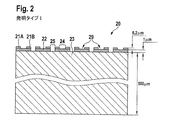
この概念による第1の好ましい実施形態を、図2に示す。図2は、複数のTHzアンテナ29を有するTHzアンテナアレー20の断面図であり、THzアンテナ29は光導電領域22と、第1電極21Aと、第2電極21Bとを備える。電極21A、21Bは、光導電領域22の少なくとも一部分の上を横方向(水平方向)に延びるスペース領域24によって間隔を空けて配置される。本発明の概念によれば、アレー20において隣接するTHzアンテナ29間の横方向領域25は非光導電性構造である。本実施形態は、領域25に光導電性材料を設けない。この場合、光導電領域22は、スペース領域24と電極21A、21Bの横方向を超えない横方向の伸展部(水平部)に限定される。光導電領域は、THz放射に有利な短い電荷キャリア寿命を有するLT−GaAsから形成される。これは、一般に光導電材料に使用されるGaAs基板(LT−GaAsに比べて比較的長い電荷キャリア寿命を有しかつ比較的不利な散乱および減衰特性を有する)に勝る利点を有する。電極21A、21Bの厚みは、約200nmである。光導電領域の厚みは約1,000nmであり、したがって、一般に使用される光導電層より明らかに薄い。基板の厚みは、500μmの範囲内である。図2に示される実施形態では、基板は、光透過性、光非導電性の基板としてサファイア基板23で形成されている。これは、THzおよび光周波数領域の両方において特に小さい散乱および減衰を示す。
A first preferred embodiment according to this concept is shown in FIG. FIG. 2 is a cross-sectional view of a
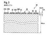
図3は、同じく複数のTHzアンテナを有するTHzアンテナアレー30の特に好ましい別の実施形態を示し、THzアンテナ39は、光導電領域32と、光導電領域32の少なくとも一部分を覆って横方向に延びるスペース領域34によって間隔を空けて配置された第1電極31Aおよび第2電極31Bとを備える。THzアンテナ39は、非ドープシリコン基板33上に形成されている。層の厚みは、図2における層と同様に生成される。
FIG. 3 shows another particularly preferred embodiment of a
図3に示される実施形態では、電極31A、31Bは「埋込み式」である。図2に示される実施形態とは異なり、光導電領域32は、図2におけるように電極31A、31Bの下側に配置されかつスペーサ領域34の横方向の伸展部および電極31A、31Bに延びる層32Aに加えて、別の光導電層32Bを有する。この光導電領域はまた、電極31A、31B間に配置され、この場合はスペース領域34の横方向の伸展部(水平部)のみに延びる層32Bを有する。
In the embodiment shown in FIG. 3, the
図4は、図2および図3の断面図に示される実施形態の平面図であり、同じ参照符号が相応して使用されている。この図では、電極21A、21B、31A、31Bのフィンガ構造が明らかである。
FIG. 4 is a plan view of the embodiment shown in the cross-sectional views of FIGS. 2 and 3, and the same reference numerals are used accordingly. In this figure, the finger structure of the
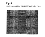
図5は、図2に示される実施形態によるTHzアンテナアレーの構造を示す、即ち出発材料からのエピタキシャルリフトオフよりも前のTHzアンテナアレーを示す適切な倍率の顕微鏡写真である。 FIG. 5 is a photomicrograph at a suitable magnification showing the structure of the THz antenna array according to the embodiment shown in FIG. 2, ie showing the THz antenna array prior to the epitaxial lift-off from the starting material.
本製造方法では、出発材料は、図8(a)に概略的に示されているように準備される。この場合、100nmのGaAs(図示せず)、犠牲層としての100nmのAlAs52および厚みが500nm〜2000nmの範囲のLT−GaAs層53で構成されるエピタキシャル付着(epitaxially applied)されたヘテロ構造層を有するGaAs基板51である。
In this production method, the starting material is prepared as schematically shown in FIG. 8 (a). In this case, it has an epitaxially applied heterostructure layer composed of 100 nm GaAs (not shown), 100 nm AlAs 52 as a sacrificial layer, and an LT-
図8(b)のフィンガ構造体54の形体の電極の形成は、一方の手順では、感光性コーティング上でのスピニングおよびこれに続くリソグラフィによって実行できる。これに続いて、電極物質の金属蒸着が行われ、次に、アセトン内での感光性コーティングの溶解による不要な金属表面のリフトオフが実行される。他方の手順では、まず金属蒸着を行ない、次に感光性コーティング上のスピニング、続いてリソグラフィを実施することができる。これに続いて、不要な金属電極部位の湿式化学エッチングが実行される。
The formation of an electrode in the form of a
図5に示される方法の段階では、感光性コーティングのスピニングが追加実行され、次にリソグラフィが実行される。この後、図8(c)のように、アレー内の隣接するTHzアンテナ間のLT−GaAs横方向領域が、湿式化学手段または乾式化学手段によってエッチングされ除去される。 In the method step shown in FIG. 5, additional spinning of the photosensitive coating is performed, followed by lithography. Thereafter, as shown in FIG. 8C, the LT-GaAs lateral region between adjacent THz antennas in the array is etched and removed by wet chemical means or dry chemical means.
図8(d)のとおり、例えばフッ化水素酸におけるAlAs犠牲層の湿式化学エッチングの結果として、図5に示すアンテナアレー構造体52全体のエピタキシャルリフトオフ(剥離)が発生する。
As shown in FIG. 8D, for example, as a result of the wet chemical etching of the AlAs sacrificial layer in hydrofluoric acid, the epitaxial lift-off (peeling) of the entire
図6は、詳細には示されていない図8(e)に示す支持基板55上への転写を行った後の図5におけるTHzアンテナアレーを示す。基板55は、THz領域において比較的少ない吸収および散乱を示す非ドープシリコンであってもよく、また任意選択として、および追加的に、サファイアまたは石英ガラス等の光透過基板であってもよい。図8(f)は、本製造プロセスの終わりにおける最終的なTHzアンテナアレーを示す。
FIG. 6 shows the THz antenna array in FIG. 5 after transfer onto the
図5および図6に示される顕微鏡写真は詳細なものである。GaAs出発基板51上では多数のアンテナアレーが並行処理されるため、製造においては比較的多量の個体数が得られる。
The micrographs shown in FIGS. 5 and 6 are detailed. Since a large number of antenna arrays are processed in parallel on the
図7は、本発明によるTHzアンテナアレー40の特に好ましい別の実施形態を示す、図4に類似する概略平面図であり、同様に、電極41A、41Bのフィンガ構造がスペース領域44の介在を伴って示されている。このスペース領域44は、光導電領域42の少なくとも一部分を覆って横方向に延びる。アレー40内のTHzアンテナ49は、図5および図6を参照して説明された製造方法に従って非ドープシリコン基板43上に形成される。フィンガ構造体のフィンガ状電極41A、41Bは、THz共振器の形成に寄与する光導電領域(電極41A、41B間の方形状領域48)から離れた方向を向くT字形状体46を、横方向の伸展部において有する。
FIG. 7 is a schematic plan view similar to FIG. 4 showing another particularly preferred embodiment of a
さらに、より詳しくは示されていないが、第1の複数のTHzアンテナ49’は、第2の複数のTHzアンテナ49’’とは異なる電位に設定できる。その結果、特に、前記共振器46を別々に制御することができ、および/またはアレー全体の放射特性を有利に変調することができる。
Furthermore, although not shown in more detail, the first plurality of THz antennas 49 'can be set to a different potential than the second plurality of
上述のTHzアンテナアレー20、30、40の製造に関するこれまでに述べたマイクロ技術手法は、さらに、ナノテクノロジー、光通信学およびマイクロシステム方法を利用することによって、達成可能なTHz出力信号パワーを好ましくは少なくとも10倍は向上することができる。これら方法を利用することによって、製造コストが増大してしまうことはほとんどない。このため、図9は上述のTHzアンテナアレー20、30、40の概略図を示している。この場合、詳細には、斜線で示される光励起において、具体的には光導電領域22、32、42におい同一のTHzアンテナ29、39、49、49’、49’’を示している。この光励起は、第1電極21A、31A、41Aと第2電極21B、31B、41Bとの間の改良によって既に集光されており、詳細には示されていないTHz透過基板を通してTHz放射53が取り出される。すなわち、光は透過方向の励起側から出ていく。光励起が集中されるこの改良された概念は、ここでは詳細に示されていない、THzアンテナに対する励起側のマイクロレンズの配列によって達成可能である。図9には詳細に示されていない隣接する2つのTHzアンテナ間の間隔を、例えば、本図のように金属−半導体−金属配列(MSMアンテナ)でTHz波長のλ/2の長さまで拡大することにより、THzアンテナアレーの利得は大幅に向上される。
The previously described microtechniques for the fabrication of the
図10および図11は、これらの、および他の改良を示し、これらは、第1に構成要素設計に関連し、第2に光励起に関連し、第3に金属ナノ粒子による半導体表面の機能化による効率向上に関連する。本事例の場合、これらはTHzアンテナアレー50の別の好ましい実施形態において実現され、アンテナアレーの古典的場の理論の電位を改良した形で利用する。この場合、個々のMSMアンテナ素子59の、例えば図9または先行する各図に示されている間隔DをTHz放射の波長の例えばλ/20からλ/2の長さまで拡大することにより、THzアンテナアレーの配列の利得を大幅に向上させることができ、その結果、周囲の全体システムにおける光学的損失は著しく低減される。この利得は、個々のアンテナ59の電磁結合にも依存するが、これも同様に、屈折率の適合化などの有利な方策によって改善することが可能である。個々のMSMアンテナ素子59の間隔Dを拡大する上述の方策によって、必要に応じて、前記利得は10倍またはそれ以上まで増加することができる。
FIGS. 10 and 11 show these and other improvements, which are first related to component design, second related to photoexcitation, and third to semiconductor surface functionalization with metal nanoparticles. It is related to the efficiency improvement by. In the present case, these are implemented in another preferred embodiment of the
アンテナの間隔Dの拡大は、中間の不活性表面の拡大、即ち先の図面に示されているスペース領域24、34、44の拡大を意味する可能性がある。図10に示されるTHzアンテナアレー50の実施形態において、図9で説明されたマイクロレンズを用いる収束の概念を進展させて、マイクロレンズアレー55が、THzアンテナアレー50におけるTHzアンテナ59よりも上方の励起側に組み込まれる。マイクロレンズアレー55は本装置の構成要素である。マイクロレンズアレー55は、光励起ビームとなる光励起51をTHzアンテナアレーにおいて反復して配置されたアンテナ59上に集光させる。この方法では、図10に示されるとおり、活性領域のみを、即ち先の図面に示されるスペース領域24、34、44を照射することが可能であり、およびこの方法では、光励起エネルギーをより効率的に利用できる。このため、特にTHzアンテナアレー50上に設けられるマイクロレンズアレーは、要求されるアンテナ間隔Dに適合するように設計可能である。さらに、光励起51を一方の電極21A、31A、41Aと他方の電極21B、31B、41Bとの間のスペース領域24、34、44上に集光させる場合、集光に必要な実際の面積をスペース領域24、34、44の伸展部よりも小さくなるように設計できることも立証されている。また、結局は、スペース領域の伸展部よりも下側にこのタイプの光励起51が集光することから、スペース領域24、34、44に生成される電荷キャリアはその利用できる容積が大きく、これによりスクリーニング効果は低減される。その結果、効率が向上することも判明している。また、光学的集中(集光)を中心よりも陽極に近づけて生成する、または、陰極に近づけて集中させることは、これにより同じくスクリーニング効果が比較的低く維持され、これによりTHz放射の効率を高めることができることから有利である場合がある。
Increasing the antenna spacing D may mean an expansion of the intermediate inert surface, ie the expansion of the
THz信号発生における別の改良は、本事例の場合のように、例えば、相互に分離される金のナノ粒子から成る蒸着層である半導体表面の改質過程において達成できる。本事例では、高い誘電定数を有する、数ナノメートルの範囲の直径を有する粒子形状の金属および他の材料が、センサ表面を大きくするためだけでなく、光励起によって生成される電荷キャリアの場の力学に影響を与えるためにも使用される。具体的には、励起によって表面プラズモン共鳴が達成され、また粒子サイズおよび密度の関数として、様々な吸収特性を生成することができる。このような金属ナノ粒子のすぐ近くにプラズモン励起の場合に高強度の場が発生するが、これを、例えば本THzアンテナアレーの感度を向上させるために利用することもできる。本事例では、この改良において、層61における金属ナノ粒子の光プラズモン共鳴特性を変換効率の上昇に利用できることが認識されている。本事例では、これは、エミッタとして設計されるTHzアレー50の光導電効率を高める作用をし、または光導電検出器の感度を高める作用もする。図11は、図10におけるTHzアンテナアレー50を三次元的に示したものである。マイクロレンズアレー55は、上述のとおり、THzアンテナアレー50と統合されてTHz放射成分を形成することができる。本事例の場合、図11にはフィンガ構造であるTHzアンテナ配列が概略的に示され、その上に、機能化されたナノスケール表面61が推定位置で示されている。
Another improvement in THz signal generation can be achieved, for example, in the process of modifying the semiconductor surface, which is a deposited layer of gold nanoparticles separated from one another, as in the present case. In this case, particle-shaped metals and other materials with diameters in the range of a few nanometers with high dielectric constants are used not only to enlarge the sensor surface, but also to the dynamics of the field of charge carriers generated by photoexcitation. Also used to affect. Specifically, surface plasmon resonance is achieved by excitation, and various absorption properties can be generated as a function of particle size and density. In the case of plasmon excitation, a high-intensity field is generated in the immediate vicinity of such metal nanoparticles, and this can be used, for example, to improve the sensitivity of the THz antenna array. In this case, it is recognized that in this improvement, the optical plasmon resonance characteristics of the metal nanoparticles in the
本事例の場合、このような表面61は低コストのプロセスとして、例えばSiO2表面上に金のナノ粒子を蒸着する過程で得ることができる。図12は、このような例を示す。電子ビーム気化プロセスを用いて、高さ2ナノメートルおよび直径3〜6ナノメートルを有する金粒子が約20ナノメートルの平均間隔で製造される。これに関連して、図12のAFM写真はAu粒子の明確な分離を示している。これは、例えば図9または図10に示すようなエミッタにおけるTHz変換の効率向上効果を得る上で特に適する。図1〜図8に示されているTHzアンテナアレーは、このために使用できる。
In this case, such a
21A,21B 電極
22 光導電領域
24 スペース領域
25 横方向領域
29 テラヘルツアンテナ
21A,
Claims (31)
前記テラヘルツアンテナ(29、39、49、49’、49’’)は、光導電領域(22、32、42)、第1電極(21A、31A、41A)、および第2電極(21B、31B、41B)を備え、
前記電極は、前記光導電領域(22、32、42)の少なくとも一部分上を水平方向に延びるスペース領域(24、34、44)によって間隔を空けて配置され、
隣接するテラヘルツアンテナ(29、39、49、49’、49’’)間の横方向領域(25、35、45)は非光導電性である、テラヘルツアンテナアレー(20、30、40、50)。 A terahertz antenna array (20, 30, 40, 50) having a plurality of terahertz antennas (29, 39, 49, 49 ′, 49 ″),
The terahertz antenna (29, 39, 49, 49 ′, 49 ″) includes a photoconductive region (22, 32, 42), a first electrode (21A, 31A, 41A), and a second electrode (21B, 31B, 41B)
The electrodes are spaced apart by a space region (24, 34, 44) extending horizontally over at least a portion of the photoconductive region (22, 32, 42);
The lateral regions (25, 35, 45) between adjacent terahertz antennas (29, 39, 49, 49 ′, 49 ″) are non-photoconductive, terahertz antenna arrays (20, 30, 40, 50) .
少なくとも第1の複数のテラヘルツアンテナアレー(20、30、40、50)は第2の複数のテラヘルツアンテナアレー(20、30、40、50)とは異なる電位にある、システム。 A system comprising a plurality of terahertz antenna arrays (20, 30, 40, 50) according to any of claims 1 to 21,
The system wherein at least the first plurality of terahertz antenna arrays (20, 30, 40, 50) are at a different potential than the second plurality of terahertz antenna arrays (20, 30, 40, 50).
THzアンテナ(22、39、49’、49’’)は、光導電領域(22、32、42)、第1電極(21A、31A、41A)、および第2電極(21B、31B、41B)を備え、前記電極は、前記光導電領域(22、32、42)の少なくとも一部分上を横方向に延びるスペース領域(24、34、44)によって間隔を空けて配置されており、
−光導電領域(22、32、42)を有する出発材料(51)を準備し、
−前記光導電領域(22、32、42)上に前記電極(21A、21B、31A、31B、41A、41B)を形成し、
−前記アレー(20、30、40、50)内の隣接するテラヘルツアンテナ(29、39、49、49’、49’’)間の横方向領域(25、35、45)における前記光導電領域(22、32、42)の一部を除去し、前記アレー(20、30、40、50)にいおける隣接するテラヘルツアンテナ(29、39、49、49’、49’’)間の横方向領域(25、35、45)は非光導電構造とし、
−得られたテラヘルツアンテナアレー(20、30、40、50)の構造体を前記出発材料からリフトオフして非光導電基板に転写する、テラヘルツアレーの製造方法。 A method of manufacturing a terahertz antenna array (20, 30, 40, 50) having a plurality of terahertz antennas (29, 39, 49, 49 ′, 49 ″),
The THz antenna (22, 39, 49 ′, 49 ″) includes a photoconductive region (22, 32, 42), a first electrode (21A, 31A, 41A), and a second electrode (21B, 31B, 41B). The electrodes are spaced apart by a space region (24, 34, 44) extending laterally over at least a portion of the photoconductive region (22, 32, 42);
Providing a starting material (51) having photoconductive regions (22, 32, 42);
-Forming the electrodes (21A, 21B, 31A, 31B, 41A, 41B) on the photoconductive regions (22, 32, 42);
The photoconductive region (25, 35, 45) in the lateral region (25, 35, 45) between adjacent terahertz antennas (29, 39, 49, 49 ′, 49 ″) in the array (20, 30, 40, 50); 22, 32, 42) in a lateral region between adjacent terahertz antennas (29, 39, 49, 49 ′, 49 ″) in the array (20, 30, 40, 50) (25, 35, 45) are non-photoconductive structures,
A method for manufacturing a terahertz array, wherein the structure of the obtained terahertz antenna array (20, 30, 40, 50) is lifted off from the starting material and transferred to a non-photoconductive substrate.
Applications Claiming Priority (2)
| Application Number | Priority Date | Filing Date | Title |
|---|---|---|---|
| DE102006014801A DE102006014801A1 (en) | 2006-03-29 | 2006-03-29 | Terahertz antenna-array, has electrodes arranged at distance over displacement region, and lateral region formed between antennas of array in non-conducting manner, where lateral region is free from practically non-conductive material |
| PCT/EP2007/002790 WO2007112925A1 (en) | 2006-03-29 | 2007-03-29 | THz ANTENNA ARRAY, SYSTEM AND METHOD FOR PRODUCING A THz ANTENNA ARRAY |
Publications (2)
| Publication Number | Publication Date |
|---|---|
| JP2009531841A true JP2009531841A (en) | 2009-09-03 |
| JP2009531841A5 JP2009531841A5 (en) | 2011-05-19 |
Family
ID=38267950
Family Applications (1)
| Application Number | Title | Priority Date | Filing Date |
|---|---|---|---|
| JP2009501952A Pending JP2009531841A (en) | 2006-03-29 | 2007-03-29 | Terahertz antenna array, terahertz antenna array system, and method for manufacturing terahertz antenna array |
Country Status (5)
| Country | Link |
|---|---|
| US (1) | US8581784B2 (en) |
| EP (1) | EP1999456B1 (en) |
| JP (1) | JP2009531841A (en) |
| DE (1) | DE102006014801A1 (en) |
| WO (1) | WO2007112925A1 (en) |
Cited By (6)
| Publication number | Priority date | Publication date | Assignee | Title |
|---|---|---|---|---|
| JP4534027B1 (en) * | 2010-03-01 | 2010-09-01 | 国立大学法人 岡山大学 | Electromagnetic wavefront shaping element, electromagnetic wave imaging apparatus including the same, and electromagnetic wave imaging method |
| JP2015513067A (en) * | 2012-01-23 | 2015-04-30 | ザ・リージェンツ・オブ・ザ・ユニバーシティ・オブ・ミシガンThe Regents Of The University Of Michigan | Photoconductive device having a plasmon electrode |
| CN106486729A (en) * | 2016-09-29 | 2017-03-08 | 东南大学 | Compact closed-loop resonator based on artificial surface phasmon |
| US10863895B2 (en) | 2015-05-27 | 2020-12-15 | The Regents Of The University Of California | Terahertz endoscopy through laser-driven terahertz sources and detectors |
| US11249017B2 (en) | 2017-04-20 | 2022-02-15 | The Regents Of The University Of California | Systems and methods for high frequency nanoscopy |
| US11906424B2 (en) | 2019-10-01 | 2024-02-20 | The Regents Of The University Of California | Method for identifying chemical and structural variations through terahertz time-domain spectroscopy |
Families Citing this family (18)
| Publication number | Priority date | Publication date | Assignee | Title |
|---|---|---|---|---|
| DE102008023991A1 (en) * | 2008-05-16 | 2009-12-03 | Forschungszentrum Dresden - Rossendorf E.V. | Scalable terahertz antennas, their manufacture and use |
| DE102008031751B3 (en) * | 2008-07-04 | 2009-08-06 | Batop Gmbh | Photo-conductive antenna for material analysis in terahertz spectral range, has lens array comprising flat-convex lenses, whose focal points are found at surface between beginnings of spiral arms in center of antenna rows |
| US8563955B2 (en) | 2009-06-12 | 2013-10-22 | Baden-Wurttemberg Stiftung Ggmbh | Passive terahertz radiation source |
| US8642964B2 (en) * | 2010-08-31 | 2014-02-04 | The United States of America, as represented by the Secretary of Commerce, NIST | High repetition rate photoconductive terahertz emitter using a radio frequency bias |
| WO2012057710A1 (en) * | 2010-10-29 | 2012-05-03 | Agency For Science, Technology And Research | THz PHOTOMIXER EMITTER AND METHOD |
| JP2012222303A (en) * | 2011-04-13 | 2012-11-12 | Seiko Epson Corp | Terahertz wave generator, camera, imaging apparatus, and measuring apparatus |
| JP5765086B2 (en) * | 2011-06-24 | 2015-08-19 | セイコーエプソン株式会社 | Terahertz wave generator, camera, imaging device, and measuring device |
| DE102012010926A1 (en) | 2012-06-04 | 2013-12-05 | Amo Gmbh | Photoconductive structure e.g. radiation source, for optical generation of field signals in terahertz- frequency range in bio analysis, has metallic layers formed from locations and provided in direct contact with semiconductor material |
| US9136421B2 (en) | 2013-01-15 | 2015-09-15 | Electronics And Telecommunications Research Institute | Wide area array type photonic crystal photomixer for generating and detecting broadband terahertz wave |
| JP6955337B2 (en) * | 2014-06-13 | 2021-10-27 | ザ リージェンツ オブ ザ ユニバーシティ オブ カリフォルニアThe Regents Of The University Of California | Low Duty Cycle Continuous Wave Photoconducting Terahertz Imaging and Spectroscopy System |
| GB2546654B (en) * | 2014-10-30 | 2021-06-02 | Mitsubishi Electric Corp | Array antenna apparatus and method for manufacturing the same |
| US10436780B2 (en) * | 2015-06-04 | 2019-10-08 | Purdue Research Foundation | Multi-site particle sensing system |
| KR102257556B1 (en) * | 2016-03-03 | 2021-05-31 | 한국전자통신연구원 | Apparatus for generating terahertz wave and method for controlling terahertz wavefront using the same |
| RU2622093C9 (en) * | 2016-05-13 | 2017-07-25 | Государственное образовательное учреждение высшего профессионального образования Кыргызско-Российский Славянский университет (КРСУ) | Source of terahertz radiation |
| DE102016116900B3 (en) * | 2016-09-09 | 2017-11-16 | Helmholtz-Zentrum Dresden - Rossendorf E.V. | THz antenna and device for transmitting and / or receiving THz radiation |
| DE102016011383A1 (en) | 2016-09-21 | 2018-03-22 | Batop Gmbh | Photoconductive antenna for generating or receiving terahertz radiation |
| RU201847U1 (en) * | 2020-10-21 | 2021-01-15 | Федеральное государственное бюджетное образовательное учреждение высшего образования «Сибирский государственный университет геосистем и технологий» (СГУГиТ) | Photoconductive antenna array |
| CN112510352A (en) * | 2020-11-04 | 2021-03-16 | 西南科技大学 | Terahertz wave radiation method and system of microstructure photoconductive antenna |
Citations (3)
| Publication number | Priority date | Publication date | Assignee | Title |
|---|---|---|---|---|
| JP2005311324A (en) * | 2004-03-26 | 2005-11-04 | Canon Inc | Photosemiconductor device and its manufacturing method |
| JP2005538542A (en) * | 2002-09-04 | 2005-12-15 | テラビュー リミテッド | Electrodes on photoconductive substrates for generation and detection of terahertz radiation |
| JP2006064691A (en) * | 2004-07-30 | 2006-03-09 | Canon Inc | Sensing apparatus |
Family Cites Families (5)
| Publication number | Priority date | Publication date | Assignee | Title |
|---|---|---|---|---|
| US5401953A (en) * | 1993-09-23 | 1995-03-28 | The United States Of America As Represented By The Administrator Of The National Aeronautics And Space Administration | Optically-switched submillimeter-wave oscillator and radiator having a switch-to-switch propagation delay |
| US5663639A (en) | 1994-01-18 | 1997-09-02 | Massachusetts Institute Of Technology | Apparatus and method for optical heterodyne conversion |
| US20040196660A1 (en) | 2001-09-21 | 2004-10-07 | Mamoru Usami | Terahertz light apparatus |
| US7615787B2 (en) * | 2004-03-26 | 2009-11-10 | Canon Kabushiki Kaisha | Photo-semiconductor device and method of manufacturing the same |
| DE102004046123A1 (en) * | 2004-09-23 | 2006-08-24 | Forschungszentrum Rossendorf E.V. | Coherent terahertz radiation source |
-
2006
- 2006-03-29 DE DE102006014801A patent/DE102006014801A1/en not_active Withdrawn
-
2007
- 2007-03-29 US US12/294,442 patent/US8581784B2/en not_active Expired - Fee Related
- 2007-03-29 JP JP2009501952A patent/JP2009531841A/en active Pending
- 2007-03-29 WO PCT/EP2007/002790 patent/WO2007112925A1/en active Application Filing
- 2007-03-29 EP EP07723734.5A patent/EP1999456B1/en not_active Not-in-force
Patent Citations (3)
| Publication number | Priority date | Publication date | Assignee | Title |
|---|---|---|---|---|
| JP2005538542A (en) * | 2002-09-04 | 2005-12-15 | テラビュー リミテッド | Electrodes on photoconductive substrates for generation and detection of terahertz radiation |
| JP2005311324A (en) * | 2004-03-26 | 2005-11-04 | Canon Inc | Photosemiconductor device and its manufacturing method |
| JP2006064691A (en) * | 2004-07-30 | 2006-03-09 | Canon Inc | Sensing apparatus |
Non-Patent Citations (1)
| Title |
|---|
| JPN5009002944; DREYHAUPT A: CONFERENCE DIGEST OF THE 2004 JOINT 29TH INTERNATIONAL CONFERENCE ON INFRARED AND MILLIMETER WAVES A , 20040927, P83-84, IEEE * |
Cited By (12)
| Publication number | Priority date | Publication date | Assignee | Title |
|---|---|---|---|---|
| JP4534027B1 (en) * | 2010-03-01 | 2010-09-01 | 国立大学法人 岡山大学 | Electromagnetic wavefront shaping element, electromagnetic wave imaging apparatus including the same, and electromagnetic wave imaging method |
| WO2011108518A1 (en) * | 2010-03-01 | 2011-09-09 | 国立大学法人 岡山大学 | Electromagnetic wave wavefront shaping element and electromagnetic wave imaging device using the same, and method of electromagnetic wave imaging |
| JP2011179989A (en) * | 2010-03-01 | 2011-09-15 | Okayama Univ | Electromagnetic wavefront shaping element, electromagnetic wave imaging device provided with the same, and electromagnetic wave imaging method |
| JP2015513067A (en) * | 2012-01-23 | 2015-04-30 | ザ・リージェンツ・オブ・ザ・ユニバーシティ・オブ・ミシガンThe Regents Of The University Of Michigan | Photoconductive device having a plasmon electrode |
| US9804026B2 (en) | 2012-01-23 | 2017-10-31 | The Regents Of The University Of Michigan | Photoconductive emitter device with plasmonic electrodes |
| US11112305B2 (en) | 2012-01-23 | 2021-09-07 | The Regents Of The University Of California | Photoconductive detector device with plasmonic electrodes |
| US11231318B2 (en) | 2012-01-23 | 2022-01-25 | The Regents Of The University Of California | Photoconductive detector device with plasmonic electrodes |
| US10863895B2 (en) | 2015-05-27 | 2020-12-15 | The Regents Of The University Of California | Terahertz endoscopy through laser-driven terahertz sources and detectors |
| CN106486729A (en) * | 2016-09-29 | 2017-03-08 | 东南大学 | Compact closed-loop resonator based on artificial surface phasmon |
| CN106486729B (en) * | 2016-09-29 | 2021-05-04 | 东南大学 | Compact closed-loop resonator based on artificial surface plasmon |
| US11249017B2 (en) | 2017-04-20 | 2022-02-15 | The Regents Of The University Of California | Systems and methods for high frequency nanoscopy |
| US11906424B2 (en) | 2019-10-01 | 2024-02-20 | The Regents Of The University Of California | Method for identifying chemical and structural variations through terahertz time-domain spectroscopy |
Also Published As
| Publication number | Publication date |
|---|---|
| US8581784B2 (en) | 2013-11-12 |
| EP1999456B1 (en) | 2016-07-20 |
| EP1999456A1 (en) | 2008-12-10 |
| US20110080329A1 (en) | 2011-04-07 |
| WO2007112925A1 (en) | 2007-10-11 |
| DE102006014801A1 (en) | 2007-10-04 |
Similar Documents
| Publication | Publication Date | Title |
|---|---|---|
| JP2009531841A (en) | Terahertz antenna array, terahertz antenna array system, and method for manufacturing terahertz antenna array | |
| US11231318B2 (en) | Photoconductive detector device with plasmonic electrodes | |
| US7791291B2 (en) | Diamond field emission tip and a method of formation | |
| US8638035B2 (en) | Terahertz radiation sources and methods of manufacturing the same | |
| EP1010997B1 (en) | Three-dimensional periodical structure, its manufacturing method, and method of manufacturing film | |
| US7608814B2 (en) | Optical structure for localising an electromagnetic field and detector or emitter device including such a structure | |
| US7728397B2 (en) | Coupled nano-resonating energy emitting structures | |
| JP2009531841A5 (en) | ||
| JP2005538542A (en) | Electrodes on photoconductive substrates for generation and detection of terahertz radiation | |
| US20090284126A1 (en) | Vacuum Electronic Devices and Cavities and Fabrication Methods Therefor | |
| JP5222950B2 (en) | High-speed plasmonic devices to enhance the performance of microelectronic devices | |
| US8153999B2 (en) | Terahertz wave generating device and apparatus using the same | |
| US7791053B2 (en) | Depressed anode with plasmon-enabled devices such as ultra-small resonant structures | |
| US7710040B2 (en) | Single layer construction for ultra small devices | |
| US10622181B2 (en) | Nanoscale field-emission device and method of fabrication | |
| CN109781250B (en) | Photosensitive imaging detection chip based on tip electron fluorescence excitation and preparation method thereof | |
| CN110767519B (en) | Field emission electron source structure and forming method thereof, electron source and microwave tube | |
| JP2007324310A (en) | Electromagnetic wave generator | |
| US20110169404A1 (en) | Traveling wave electron device with membrane-supported slow wave circuit | |
| EP3836232B1 (en) | Three-dimensional photoconductive transducer for terahertz signals or picosecond electrical pulses | |
| CN218632058U (en) | AlGaN-based plasmon polariton photoelectric detector structure | |
| CN111370276A (en) | Vacuum channel type photoelectric cathode and preparation method thereof | |
| JPH11266055A (en) | Semiconductor light-emitting device and manufacture thereof | |
| CN116125573A (en) | Method for realizing energy valley emission direction separation of two-dimensional material by utilizing electron beam | |
| CN117091697A (en) | Broadband microcavity array coupling structure for quantum well detector and preparation method thereof |
Legal Events
| Date | Code | Title | Description |
|---|---|---|---|
| A621 | Written request for application examination |
Free format text: JAPANESE INTERMEDIATE CODE: A621 Effective date: 20100325 |
|
| A521 | Written amendment |
Free format text: JAPANESE INTERMEDIATE CODE: A523 Effective date: 20110315 |
|
| A977 | Report on retrieval |
Free format text: JAPANESE INTERMEDIATE CODE: A971007 Effective date: 20121121 |
|
| A131 | Notification of reasons for refusal |
Free format text: JAPANESE INTERMEDIATE CODE: A131 Effective date: 20130219 |
|
| A601 | Written request for extension of time |
Free format text: JAPANESE INTERMEDIATE CODE: A601 Effective date: 20130517 |
|
| A602 | Written permission of extension of time |
Free format text: JAPANESE INTERMEDIATE CODE: A602 Effective date: 20130524 |
|
| A601 | Written request for extension of time |
Free format text: JAPANESE INTERMEDIATE CODE: A601 Effective date: 20130612 |
|
| A602 | Written permission of extension of time |
Free format text: JAPANESE INTERMEDIATE CODE: A602 Effective date: 20130619 |
|
| A521 | Written amendment |
Free format text: JAPANESE INTERMEDIATE CODE: A523 Effective date: 20130712 |
|
| A02 | Decision of refusal |
Free format text: JAPANESE INTERMEDIATE CODE: A02 Effective date: 20140128 |