JP2009246337A - Semiconductor device and method of manufacturing the same - Google Patents
Semiconductor device and method of manufacturing the same Download PDFInfo
- Publication number
- JP2009246337A JP2009246337A JP2008328986A JP2008328986A JP2009246337A JP 2009246337 A JP2009246337 A JP 2009246337A JP 2008328986 A JP2008328986 A JP 2008328986A JP 2008328986 A JP2008328986 A JP 2008328986A JP 2009246337 A JP2009246337 A JP 2009246337A
- Authority
- JP
- Japan
- Prior art keywords
- semiconductor device
- bonding pad
- manufacturing
- shape
- connection bump
- Prior art date
- Legal status (The legal status is an assumption and is not a legal conclusion. Google has not performed a legal analysis and makes no representation as to the accuracy of the status listed.)
- Pending
Links
Images


Classifications
-
- H—ELECTRICITY
- H01—ELECTRIC ELEMENTS
- H01L—SEMICONDUCTOR DEVICES NOT COVERED BY CLASS H10
- H01L24/00—Arrangements for connecting or disconnecting semiconductor or solid-state bodies; Methods or apparatus related thereto
- H01L24/01—Means for bonding being attached to, or being formed on, the surface to be connected, e.g. chip-to-package, die-attach, "first-level" interconnects; Manufacturing methods related thereto
- H01L24/10—Bump connectors ; Manufacturing methods related thereto
- H01L24/15—Structure, shape, material or disposition of the bump connectors after the connecting process
- H01L24/16—Structure, shape, material or disposition of the bump connectors after the connecting process of an individual bump connector
-
- H—ELECTRICITY
- H01—ELECTRIC ELEMENTS
- H01L—SEMICONDUCTOR DEVICES NOT COVERED BY CLASS H10
- H01L2224/00—Indexing scheme for arrangements for connecting or disconnecting semiconductor or solid-state bodies and methods related thereto as covered by H01L24/00
- H01L2224/01—Means for bonding being attached to, or being formed on, the surface to be connected, e.g. chip-to-package, die-attach, "first-level" interconnects; Manufacturing methods related thereto
- H01L2224/02—Bonding areas; Manufacturing methods related thereto
- H01L2224/04—Structure, shape, material or disposition of the bonding areas prior to the connecting process
- H01L2224/05—Structure, shape, material or disposition of the bonding areas prior to the connecting process of an individual bonding area
- H01L2224/0554—External layer
- H01L2224/0556—Disposition
- H01L2224/05568—Disposition the whole external layer protruding from the surface
-
- H—ELECTRICITY
- H01—ELECTRIC ELEMENTS
- H01L—SEMICONDUCTOR DEVICES NOT COVERED BY CLASS H10
- H01L2224/00—Indexing scheme for arrangements for connecting or disconnecting semiconductor or solid-state bodies and methods related thereto as covered by H01L24/00
- H01L2224/01—Means for bonding being attached to, or being formed on, the surface to be connected, e.g. chip-to-package, die-attach, "first-level" interconnects; Manufacturing methods related thereto
- H01L2224/02—Bonding areas; Manufacturing methods related thereto
- H01L2224/04—Structure, shape, material or disposition of the bonding areas prior to the connecting process
- H01L2224/05—Structure, shape, material or disposition of the bonding areas prior to the connecting process of an individual bonding area
- H01L2224/0554—External layer
- H01L2224/05573—Single external layer
-
- H—ELECTRICITY
- H01—ELECTRIC ELEMENTS
- H01L—SEMICONDUCTOR DEVICES NOT COVERED BY CLASS H10
- H01L2224/00—Indexing scheme for arrangements for connecting or disconnecting semiconductor or solid-state bodies and methods related thereto as covered by H01L24/00
- H01L2224/01—Means for bonding being attached to, or being formed on, the surface to be connected, e.g. chip-to-package, die-attach, "first-level" interconnects; Manufacturing methods related thereto
- H01L2224/10—Bump connectors; Manufacturing methods related thereto
- H01L2224/12—Structure, shape, material or disposition of the bump connectors prior to the connecting process
- H01L2224/13—Structure, shape, material or disposition of the bump connectors prior to the connecting process of an individual bump connector
- H01L2224/13001—Core members of the bump connector
- H01L2224/13099—Material
-
- H—ELECTRICITY
- H01—ELECTRIC ELEMENTS
- H01L—SEMICONDUCTOR DEVICES NOT COVERED BY CLASS H10
- H01L2224/00—Indexing scheme for arrangements for connecting or disconnecting semiconductor or solid-state bodies and methods related thereto as covered by H01L24/00
- H01L2224/01—Means for bonding being attached to, or being formed on, the surface to be connected, e.g. chip-to-package, die-attach, "first-level" interconnects; Manufacturing methods related thereto
- H01L2224/10—Bump connectors; Manufacturing methods related thereto
- H01L2224/15—Structure, shape, material or disposition of the bump connectors after the connecting process
- H01L2224/16—Structure, shape, material or disposition of the bump connectors after the connecting process of an individual bump connector
-
- H—ELECTRICITY
- H01—ELECTRIC ELEMENTS
- H01L—SEMICONDUCTOR DEVICES NOT COVERED BY CLASS H10
- H01L2224/00—Indexing scheme for arrangements for connecting or disconnecting semiconductor or solid-state bodies and methods related thereto as covered by H01L24/00
- H01L2224/80—Methods for connecting semiconductor or other solid state bodies using means for bonding being attached to, or being formed on, the surface to be connected
- H01L2224/81—Methods for connecting semiconductor or other solid state bodies using means for bonding being attached to, or being formed on, the surface to be connected using a bump connector
- H01L2224/8119—Arrangement of the bump connectors prior to mounting
- H01L2224/81193—Arrangement of the bump connectors prior to mounting wherein the bump connectors are disposed on both the semiconductor or solid-state body and another item or body to be connected to the semiconductor or solid-state body
-
- H—ELECTRICITY
- H01—ELECTRIC ELEMENTS
- H01L—SEMICONDUCTOR DEVICES NOT COVERED BY CLASS H10
- H01L2224/00—Indexing scheme for arrangements for connecting or disconnecting semiconductor or solid-state bodies and methods related thereto as covered by H01L24/00
- H01L2224/80—Methods for connecting semiconductor or other solid state bodies using means for bonding being attached to, or being formed on, the surface to be connected
- H01L2224/81—Methods for connecting semiconductor or other solid state bodies using means for bonding being attached to, or being formed on, the surface to be connected using a bump connector
- H01L2224/8138—Bonding interfaces outside the semiconductor or solid-state body
- H01L2224/81399—Material
- H01L2224/814—Material with a principal constituent of the material being a metal or a metalloid, e.g. boron [B], silicon [Si], germanium [Ge], arsenic [As], antimony [Sb], tellurium [Te] and polonium [Po], and alloys thereof
-
- H—ELECTRICITY
- H01—ELECTRIC ELEMENTS
- H01L—SEMICONDUCTOR DEVICES NOT COVERED BY CLASS H10
- H01L2924/00—Indexing scheme for arrangements or methods for connecting or disconnecting semiconductor or solid-state bodies as covered by H01L24/00
- H01L2924/0001—Technical content checked by a classifier
- H01L2924/00014—Technical content checked by a classifier the subject-matter covered by the group, the symbol of which is combined with the symbol of this group, being disclosed without further technical details
-
- H—ELECTRICITY
- H01—ELECTRIC ELEMENTS
- H01L—SEMICONDUCTOR DEVICES NOT COVERED BY CLASS H10
- H01L2924/00—Indexing scheme for arrangements or methods for connecting or disconnecting semiconductor or solid-state bodies as covered by H01L24/00
- H01L2924/01—Chemical elements
- H01L2924/01005—Boron [B]
-
- H—ELECTRICITY
- H01—ELECTRIC ELEMENTS
- H01L—SEMICONDUCTOR DEVICES NOT COVERED BY CLASS H10
- H01L2924/00—Indexing scheme for arrangements or methods for connecting or disconnecting semiconductor or solid-state bodies as covered by H01L24/00
- H01L2924/01—Chemical elements
- H01L2924/01006—Carbon [C]
-
- H—ELECTRICITY
- H01—ELECTRIC ELEMENTS
- H01L—SEMICONDUCTOR DEVICES NOT COVERED BY CLASS H10
- H01L2924/00—Indexing scheme for arrangements or methods for connecting or disconnecting semiconductor or solid-state bodies as covered by H01L24/00
- H01L2924/01—Chemical elements
- H01L2924/01029—Copper [Cu]
-
- H—ELECTRICITY
- H01—ELECTRIC ELEMENTS
- H01L—SEMICONDUCTOR DEVICES NOT COVERED BY CLASS H10
- H01L2924/00—Indexing scheme for arrangements or methods for connecting or disconnecting semiconductor or solid-state bodies as covered by H01L24/00
- H01L2924/01—Chemical elements
- H01L2924/01033—Arsenic [As]
-
- H—ELECTRICITY
- H01—ELECTRIC ELEMENTS
- H01L—SEMICONDUCTOR DEVICES NOT COVERED BY CLASS H10
- H01L2924/00—Indexing scheme for arrangements or methods for connecting or disconnecting semiconductor or solid-state bodies as covered by H01L24/00
- H01L2924/01—Chemical elements
- H01L2924/01079—Gold [Au]
-
- H—ELECTRICITY
- H01—ELECTRIC ELEMENTS
- H01L—SEMICONDUCTOR DEVICES NOT COVERED BY CLASS H10
- H01L2924/00—Indexing scheme for arrangements or methods for connecting or disconnecting semiconductor or solid-state bodies as covered by H01L24/00
- H01L2924/01—Chemical elements
- H01L2924/01082—Lead [Pb]
-
- H—ELECTRICITY
- H01—ELECTRIC ELEMENTS
- H01L—SEMICONDUCTOR DEVICES NOT COVERED BY CLASS H10
- H01L2924/00—Indexing scheme for arrangements or methods for connecting or disconnecting semiconductor or solid-state bodies as covered by H01L24/00
- H01L2924/30—Technical effects
- H01L2924/35—Mechanical effects
- H01L2924/351—Thermal stress
Abstract
Description
本発明は、半導体装置及びその製造方法に関し、より詳しくは、フリップチップ型半導体装置及びその製造方法に関するものである。 The present invention relates to a semiconductor device and a manufacturing method thereof, and more particularly to a flip chip type semiconductor device and a manufacturing method thereof.
半導体装置は通信、ネットワーク、コンピュータ、家電製品、事務機器、カメラ、さらにはゲーム機器など、産業用機器から身回りの道具、携帯機器までさまざまな分野で利用されており、その需要は急速に成長しつつある。その急速に成長する需要に伴って、半導体装置の小型化、多ピン化、薄型化が要求されている一方、小型化、多ピン化、薄型化のために、機能を悪化させたりコストが高くなることを抑制するのみに止まることはできず、さらに高性能化と低コスト化が強く要望されている。 Semiconductor devices are used in a variety of fields, from industrial equipment to personal tools and portable equipment, such as communications, networks, computers, home appliances, office equipment, cameras, and even game machines. I am doing. Along with the rapidly growing demand, semiconductor devices are required to be downsized, multi-pin, and thin. On the other hand, functions, functions, and costs are high due to downsizing, multi-pins, and thinning. However, there is a strong demand for higher performance and lower cost.
上述の小型化、薄型化、多ピン化の目的を果たすために、IC素子(ダイと称することがある)を取り付けて、外部電極と信号のやり取りを行うために、IC素子の接続端子とリードフレームの接続方式を、従来の金細線によるワイヤボンデング型から、金細線を不要としたフリップチップ型半導体装置が開発され、それが現在の半導体装置の主流となっている。 In order to achieve the above-mentioned purpose of miniaturization, thinning, and increase in the number of pins, an IC element (sometimes referred to as a die) is attached, and in order to exchange signals with external electrodes, the connection terminals and leads of the IC element From the conventional wire bonding type using a fine gold wire to a frame connection method, a flip chip type semiconductor device that does not require a fine gold wire has been developed, and this is the mainstream of current semiconductor devices.
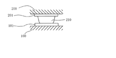
図1に示すように、半導体チップ200のマウンティングパッド201上に金属バンプ210を形成し、基板100のボンディングパッド101と上記半導体チップ200のマウンティングパッド201を上記金属バンプ210を介して熱溶融又は加圧圧着によって電気接続を行う。又、従来の回路のパターンニング工程でボンディングパッドを形成するには、ドライエッチング又はウェットエッチング法が使用されていた。ドライエッチングはボンディングパッドを寸法精度高く形成することができる一方、手数が掛ってコストが高くて不経済である。故に回路パターンニングの工程は、割とコストが低く手数が掛らないウェットエッチング法がよく使われる(例えば、特許文献1参照)。
As shown in FIG. 1,
ウェットエッチングは一般に強性酸又は強アルカリ性エッチング液を使用してエッチング液と被加工物の金属層表面と化学反応を発生させ、その拡散効果(diffusion)を利用して被加工物の所望の部位の材料を取り去る方法である。ところでウェットエッチングは同方性(isotropic)エッチングであるので、エッチング液が被加工物表面の金属層と長時間接続すると、形成される回路パターンの断面形状が大きく変形し、図4(A)に示すように、エッチングによって形成される孔部の上縁部が孔部の底部よりエッチングが進んでいく。その結果ウェットエッチングによって形成されるボンディングパッド又は金属バンプは、上面やや丸みのある形状になっていた。こうして形成されたボンディングパッド101を、金属バンプを介してとマウンティングパッドを互いに押圧して圧着すると、金属バンプは押圧されて扁平状になり、ボンディングパッドとマウンティングパッドの接合強度が弱くなる。エッチング部位の形状の変化を少なくするためにエッチング速度を早くしてエッチング液と被加工物との接触時間を短くするには、金属層の厚さを薄くする必要があり、金属層の厚さを薄くすると回路パターンが剥離しやすくなり、それによる信頼性の低下と、加工性の困難度の増加をもたらしていた。
In wet etching, a strong acid or strong alkaline etching solution is generally used to generate a chemical reaction between the etching solution and the surface of the metal layer of the workpiece, and its diffusion effect is used to obtain a desired part of the workpiece. It is a method of removing the material. By the way, since wet etching is isotropic etching, when the etching solution is connected to the metal layer on the surface of the workpiece for a long time, the cross-sectional shape of the circuit pattern to be formed is greatly deformed, as shown in FIG. In this way, the etching proceeds at the upper edge of the hole formed by etching from the bottom of the hole. As a result, the bonding pad or metal bump formed by wet etching has a slightly rounded upper surface. When the
本発明は上述の従来の技術の問題に鑑みて行われたものであって、従来のウェットエッチングによる回路パターンの欠点を改善した半導体装置とその製造方法を提供することを目的とする。 The present invention has been made in view of the above-described problems of the prior art, and an object of the present invention is to provide a semiconductor device and a method for manufacturing the same, in which a defect of a circuit pattern by conventional wet etching is improved.
本発明はさらに、ドライエッチングによるコストの浪費とエッチング選択性が悪いというような問題のない半導体装置とその製造方法を提供することを目的とする。 It is another object of the present invention to provide a semiconductor device and a method for manufacturing the same that do not have the problem of waste of cost due to dry etching and poor etching selectivity.
本発明はさらに、製造工程の信頼性の高い半導体装置とその製造方法を提供することを目的とする。 It is another object of the present invention to provide a semiconductor device having a high reliability in the manufacturing process and a manufacturing method thereof.
本発明はさらに、基板と半導体チップの接合強度の高い半導体装置とその製造方法を提供することを目的とする。 It is another object of the present invention to provide a semiconductor device having a high bonding strength between a substrate and a semiconductor chip and a method for manufacturing the same.
上記の目的を達成するために、本発明は、
表面に、内部回路に電気接続された接続バンプが形成された半導体チップと、表面の導電性金属層をウェットエッチングによって、上記接続バンプと電気接続するためのボンディングパッドを形成した基板を提供し、前記半導体チップを裏返して前記接続バンプと前記ボンディングパッドとの位置合わせを行い、前記ボンディングパッドと前記接続バンプの溶点より低い温度で前記接続バンプと前記ボンディングパッドを圧接し、前記ボンディングパッドが前記接続バンプ内に嵌入するように接合することを特徴とする、半導体装置の製造方法を提供する。
In order to achieve the above object, the present invention provides:
Provided is a substrate having a semiconductor chip on which a connection bump electrically connected to an internal circuit is formed and a bonding pad for electrically connecting the conductive metal layer on the surface to the connection bump by wet etching. The semiconductor chip is turned over to align the connection bump and the bonding pad, and the connection bump and the bonding pad are pressed against each other at a temperature lower than the melting point of the bonding pad and the connection bump. Provided is a method for manufacturing a semiconductor device, wherein the semiconductor bumps are joined so as to be fitted into connection bumps.
本発明の一実施例によれば、本発明は、コア板を提供し、前記コア板の表面をウェットエッチング法で複数のボンディングパッドを形成し、作用面上に複数の接続バンプを有する半導体チップを提供し、前記半導体チップと前記コア板を、接続バンプとボンディングパッドを互いに嵌合して電気接続を形成すべく、前記ボンディングパッドを前記接続バンプに圧接する、半導体装置の製造方法であって、前記圧接が、前記ボンディングパッド及び前記接続バンプの溶点より低い温度で行われることを特徴とする半導体装置の製造方法を提供する。 According to an embodiment of the present invention, the present invention provides a core plate, a plurality of bonding pads are formed on the surface of the core plate by a wet etching method, and a semiconductor chip having a plurality of connection bumps on the working surface A method of manufacturing a semiconductor device, wherein the semiconductor chip and the core plate are press-contacted to the connection bump so that the connection bump and the bonding pad are fitted to each other to form an electrical connection. The method of manufacturing a semiconductor device is characterized in that the pressure contact is performed at a temperature lower than a melting point of the bonding pad and the connection bump.
本発明の他の実施例によれば、本発明は、コア板を提供し、前記コア板の表面に金属層を形成し、前記金属層上に、フォトレジスト層を形成し、前記フォトレジスト層に複数の開口を設けて前記金属層を前記複数の開口に露出させ、ウェットエッチング液で前記複数の開口に露出した金属層を除去し、続いて前記フォトレジストを除去して、前記コア板の表面に、上面の断面幅が底面の断面幅より小さいボンディングパッドを複数形成した基板構造を形成し、作用面に、サイズが前記ボンディングパッドより大きい接続バンプを複数有する半導体チップを提供し、前記接続バンプと前記ボンディングパッドが互いに嵌合しあって電気的に接続されるように前記半導体チップを前記基板構造に圧接する半導体装置の製造方法で、前記圧接時の温度が、前記ボンディングパッド及び前記接続バンプの溶点より低いことを特徴とする半導体装置の製造方法を提供する。 According to another embodiment of the present invention, the present invention provides a core plate, a metal layer is formed on a surface of the core plate, a photoresist layer is formed on the metal layer, and the photoresist layer is formed. A plurality of openings are provided to expose the metal layer to the plurality of openings, the metal layer exposed to the plurality of openings is removed with a wet etchant, and then the photoresist is removed to form the core plate. A substrate structure in which a plurality of bonding pads having a cross-sectional width on the upper surface smaller than a cross-sectional width on the bottom surface is formed on the surface, and a semiconductor chip having a plurality of connection bumps on the working surface larger in size than the bonding pads is provided. A method of manufacturing a semiconductor device in which the semiconductor chip is pressed against the substrate structure so that the bump and the bonding pad are fitted and electrically connected to each other. But to provide a method of manufacturing a semiconductor device, wherein the lower point amount of the bonding pads and the connection bumps.
又、本発明は、表面に、内部の電気回路と電気的に接続された接続バンプを複数有する半導体チップと、表面にボンディングパッドを複数有する基板が、前記複数の接続バンプと複数のバンディングパッドが電気的に接続されるように圧接されてなる半導体装置であって、前記ボンディングパッドが前記接続バンプより硬質な導電性金属をウェットエッチングによって前記基板上に形成され、前記ボンディングパッドが前記接続バンプ内に嵌合され、前記接続バンプと前記ボンディングパッドの圧接が、前記ボンディングパッド及び前記接続バンプの溶点より低い温度で行われたことを特徴とする半導体装置を提供する。 According to another aspect of the present invention, a semiconductor chip having a plurality of connection bumps electrically connected to an internal electric circuit on the surface, a substrate having a plurality of bonding pads on the surface, the plurality of connection bumps and a plurality of banding pads are provided. A semiconductor device that is press-contacted so as to be electrically connected, wherein the bonding pad is formed on the substrate by wet etching with a conductive metal harder than the connection bump, and the bonding pad is formed in the connection bump. The semiconductor device is characterized in that the contact bump and the bonding pad are pressed at a temperature lower than the melting point of the bonding pad and the connection bump.
本発明の一実施例によれば、前記ボンディングパッドの上面の断面の幅は前記ボンディングパッドの底面の断面の幅より小さく、且つ前記接続バンプのサイズが前記基板のボンディングパッドのサイズより大きくしている。言い換えると、前記接続バンプは第1の接触端を有し、前記ボンディングパッドは前記基板と前記半導体チップが互いに圧接される際に前記第1の接触端に対応する第2の接触端を有し、前記第1接触端の幅が前記第2接触端より大きく形成されている。 According to an embodiment of the present invention, the width of the cross section of the upper surface of the bonding pad is smaller than the width of the cross section of the bottom surface of the bonding pad, and the size of the connection bump is larger than the size of the bonding pad of the substrate. Yes. In other words, the connection bump has a first contact end, and the bonding pad has a second contact end corresponding to the first contact end when the substrate and the semiconductor chip are pressed against each other. The width of the first contact end is larger than that of the second contact end.
要するに、本発明に係る半導体装置とその製造方法は、基板表面の導電性金属層をウェットエッチングで上面の断面の幅が底面の断面の幅より小さいボンディングパッドを形成し、サイズが前記基板のボンディングパッドのサイズより大きいと共に前記ボンディングパッドより硬度が小さい材質よりなる接続バンプを有する半導体チップを提供し、前記半導体チップと前記基板を前記接続バンプと前記ボンディングパッドが互いに嵌合して電気的に接続されるように圧接して、前記ボンディングパッドと前記接続バンプの接合強度を高め、半導体装置の製造方法の信頼性を高めるようにしたのである。 In short, in the semiconductor device and the manufacturing method thereof according to the present invention, the conductive metal layer on the substrate surface is wet-etched to form a bonding pad whose upper cross-sectional width is smaller than the bottom cross-sectional width, and the size is the bonding of the substrate. Provided is a semiconductor chip having a connection bump made of a material larger in size than the pad and having a hardness lower than that of the bonding pad, and electrically connecting the semiconductor chip and the substrate by fitting the connection bump and the bonding pad to each other. In this way, the bonding strength between the bonding pads and the connection bumps is increased to improve the reliability of the semiconductor device manufacturing method.
さらに、本発明は、従来のウェットエッチングの欠点と見なされていたエッチングの拡散現象を優点として、比較的に厚い金属層をウェットエッチングによってフリップチップ型半導体チップと基板の接合を効果的に可能とし、回路パターンの微細化と高信頼性化を可能としたのでドライエッチングによるコスト高とエッチングの選択性不良などの問題を回避することができる。 Furthermore, the present invention can effectively bond a flip chip type semiconductor chip and a substrate by wet etching of a relatively thick metal layer, with the advantage of etching diffusion phenomenon, which has been regarded as a drawback of conventional wet etching. Thus, miniaturization and high reliability of the circuit pattern can be achieved, so that problems such as high cost due to dry etching and poor etching selectivity can be avoided.
本発明のその他の優点と効果は、以下の本発明の半導体装置とその製造方法の好ましい実施態様を図面についての詳細な説明により容易に理解することができる。 Other advantages and effects of the present invention can be easily understood from the following detailed description of the drawings of preferred embodiments of the semiconductor device of the present invention and the manufacturing method thereof.
本発明に係る半導体装置の製造方法は、表面に、内部の電気回路と電気的に接続された接続バンプを有する半導体チップと、表面に設けられた導電性金属層をウェットエッチングして、前記接続バンプに対応して形成されたボンディングパッドを有する基板を提供し、前記半導体チップを裏返して、前記接続バンプと前記ボンディングパッドとを位置合わせして加圧して接合する方法であって、前記接続バンプと前記ボンディングパッドの圧接を前記ボンディングパッド及び前記接続バンプの溶点より低い温度で行い、前記ボンディングパッドが前記接続バンプ内に嵌合するように圧接することを特徴とする。 The method of manufacturing a semiconductor device according to the present invention includes wet etching a semiconductor chip having connection bumps electrically connected to an internal electric circuit on a surface and a conductive metal layer provided on the surface, and performing the connection. A method of providing a substrate having a bonding pad formed corresponding to a bump, turning the semiconductor chip over, aligning and pressing the connection bump and the bonding pad, the connection bump And the bonding pad are pressed at a temperature lower than the melting point of the bonding pad and the connection bump, and the bonding pad is pressed so as to fit into the connection bump.
又、本発明に係る半導体装置は、表面に、内部の電気回路と電気的に接続された接続バンプを有する半導体チップと、表面に設けられた導電性金属層をウェットエッチングによって、前記接続バンプに対応して形成されたボンディングパッドを有する基板が、前記接続バンプと前記ボンディングパッドが互いに圧接されて接合された半導体装置であって、前記ボンディングパッドが前記接続バンプより硬質であり、且つ前記ボンディングパッドが前記接続バンプ内に嵌合され、前記圧接が、前記ボンディングパッド及び前記接続バンプの溶点より低い温度で行われたことを特徴とする。 In addition, the semiconductor device according to the present invention has a semiconductor chip having connection bumps electrically connected to an internal electric circuit on the surface, and a conductive metal layer provided on the surface to the connection bumps by wet etching. A substrate having a bonding pad formed correspondingly is a semiconductor device in which the connection bump and the bonding pad are bonded to each other by pressure contact, the bonding pad being harder than the connection bump, and the bonding pad Is fitted into the connection bump, and the pressure contact is performed at a temperature lower than the melting point of the bonding pad and the connection bump.
次に図3及び図4(A)、(B)を参照して本発明の半導体装置及びその製造方法の一実施例を説明する。 Next, an embodiment of the semiconductor device of the present invention and the method for manufacturing the same will be described with reference to FIGS.
先ず、図3(A)、(B)に示すように、表面に導電性金属層101を有するコア板100を提供する。導電性金属層101は、銅が好ましいが、ニッケル、又は銅―ニッケル合金でも良い。次に前記金属層101上に、所定のパターンが形成されたフォトレジスト層102を形成し、露光と現像を行い。フォトレジスト層102に、金属層101が露出する開口103を形成する。
First, as shown in FIGS. 3A and 3B, a
次に、図3(C)、(D)に示すように、金属層101の露出した部分を酸性又はアルカリ性のエッチング液でエッチング(ウェットエッチング)を行って除去する。これによって、所定のパターン適合した複数のボンディングパッド110と、配線層120を形成する。
配線層120はボンディングパッド110を形成する方法と同一方法で形成される。
Next, as shown in FIGS. 3C and 3D, the exposed portion of the
The
このとき、コア板100上に半導体チップ(ダイ)を接着するためのボンディングパッド110のみを形成し、配線層120がないパッケージ用基板100’を形成することもできる。
At this time, only the
又、図4(A)、(B)に示すように、ウェットエッチングのために、拡散現象が発生して、フォトレジスト層102と金属層101の界面のエッチングが開口部の部分より進んで、エッチングされない部分の上面がその下方の部分より小さくなり、フォトレジスト層を除去した後に残された部分(アイランド)の上面形状が凸面状になる。
Also, as shown in FIGS. 4A and 4B, a diffusion phenomenon occurs due to wet etching, and etching at the interface between the
次に図4(C)に示すように、表面に内部の電気回路と電気接続された複数の接続バンプ210が形成された半導体チップ200を提供する。本実施例では、硬度が前記基板100のボンディングパッド110より低い材料で例えば錫又はハンダで前記接続バンプ210を形成する。
Next, as shown in FIG. 4C, a
又、前記接続バンプ210のサイズを、前記基板100のボンディングパッドより大きくして、前記ボンディングパッドが前記接続バンプに圧入して嵌合しうるようにする。言い換えれば、前記接続バンプ210は第1の接続端2101を有し、前記ボンディングパッド110は前記接続バンプの第1の接触端に対応する第2の接触端1101を有し、前記第1の接触端2101の幅を、前記第2の接触端1101の幅より大きくしている。
Further, the size of the
言い換えれば、本発明の他の実施例においては、ボンディングパッド110と金属バンプ210を圧接するときの対向面、即ち圧着表面(互いに平行又は不平行の表面)は大きさが違っており、前記第1接触端2101の幅を前記第2接触端1101の幅より大きくしてある。
In other words, in another embodiment of the present invention, the opposing surfaces when the
次に、前記半導体チップ200を裏返して、接続バンプである金属バンプ210とボンディングパッド110の位置合わせを行い、加熱圧接、又は加熱超音波圧接することで、金属バンプ210を有する半導体チップ200と、ボンディングパッド110を有する基板100'を圧接して、基板100'と半導体チップ200を電気的に接続する。
Next, the
前記金属バンプ210の大きさを前記ボンディングパッド110の大きさより大きくしていると共に、金属バンプ210の材料を、硬度がボンディングパッド110の硬度より小さい材料として、金属バンプ210とボンディングパッド110を電気的に接続するように圧接したので、硬度が高い方のボンディングパッド110が硬度が低い方の金属バンプ210に圧入嵌合されて、一方が他方を包むような凹凸嵌合接合構造が形成される。これによってボンディングパッド110と金属バンプ210接合強度が強くなり、従来のリフローによる接合に比べて、基板100'と半導体チップ200の応力(熱融着による応力)が少なくなるので最後にでき上がる半導体装置の信頼性が高まる。
The size of the metal bumps 210 is larger than the size of the
又、本実施例では、金属バンプ210とボンディングパッド110を圧接するときに、ボンディングパッドと金属バンプのそれぞれの溶点より低い温度で圧接を行った。例えば金属バンプをハンダで形成した場合その溶点は180℃、ボンディングパッドを銅で形成した場合その溶点は1063℃であるので、圧接時の温度は50度乃至180℃として、ハンダと銅のいずれとも溶融しない温度で圧接を行う。又、圧接の圧力の大きさと圧接時間の長さは、この技術に通常の知識を有するものが自由に設定することができる。
Further, in this embodiment, when the
金属バンプ210の硬度とボンディングパッド110の硬度はそれぞれの材料によって決められる。前の「一方が他方を包むような凹凸嵌合接合構造とするためには、包む一方(凹状になる一方)の材料硬度を包まれる一方(凸状になる一方)の材料硬度より低いものとした場合、包む一方の大きさを包まれる一方の大きさより大きくすることする。」前記の実施態様では、金属バンプ210をハンダ、ボンディングパッド110を銅としたが、それぞれの材料はハンダ対銅に限られず、大きさが大きい方の材料硬度が、大きさが小さい方の材料硬度より低いようにすれば良い。
The hardness of the
又、半導体チップ200と基板100'の間の空間を充填材料(under fill)220で充填して金属バンプ210とボンディングパッド110の接合を保護するとともに、半導体チップと基板との接合強度を高めることもできる。
In addition, the space between the
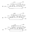
次に図5に基づいて本発明の半導体装置の変形例を説明する。図5(A)は、ボンディングパッド110の表面と金属バンプ210の表面が不平行である場合を示す。図5(B)、(C)はボンディングパッド110の表面と金属パッドの表面が平行である場合を示す。いずれの場合も接合の効果に変わりはない。
Next, a modification of the semiconductor device of the present invention will be described with reference to FIG. FIG. 5A shows a case where the surface of the
又、硬度が低い金属バンプ210の表面である第一接触端2101の幅が、硬度が高いボンディングバッド110の表面である第2接触面1101の幅より大きくしていれば、一方が他方を包むような凹凸構造となるように圧接される。
If the width of the
さらに、ボンディングパッド110又は配線回路層120の断面形状はエッチング液の種類とエッチング条件を調整することによって、三角形(図5(A)に示す)、梯形(図5(B))、又は弾丸状(図5(C))にすることができ、これらの形状は、いずれもボンディングパッドの断面の上面幅がその底面幅より小さく形成されている。
Furthermore, the cross-sectional shape of the
本発明の実施例による半導体装置は、上述の方法によって製造され、次の構成を含む、表面にウェットエッチングによって形成される複数のボンディングパッド110を有する基板100'と、作用面に複数の金属バンプ210が形成された半導体チップ210とを有する半導体装置であって、前記金属バンプ210とボンディングパッド110が圧接によって嵌合されて電気的に接続され、前記圧接は、前記ボンディングパッド110及び金属バンプの溶点より低い温度で行われ、前記ボンディングパッド110の硬度が前記金属バンプ210の硬度より高く、且つ、前記ボンディング110の上面断面幅がその底面断面幅より小さくされている。
A semiconductor device according to an embodiment of the present invention is manufactured by the above-described method, and includes a
さらに、第一接触端210の幅を第2接触端の幅より大きくしている。
Furthermore, the width of the
又、本発明の半導体装置の製造方法は、従来のウェットエッチング法で基板表面に凸出形状を呈するボンディングパッドを形成し、その上面端面の幅を底面の幅より小さくなるようにしている。そしてこうしたボンディングパッドを有する基板と、作用面に接続バンプを有する半導体チップと圧接して接合する。そして前記接続パッドは、基板のボンディングパッドのサイズより大きいサイズを有する金属バンプとしている。さらに前記金属バンプを硬度が前記ボンディングパッドの材質の硬度より低い材質より形成し、前記金属バンプ及び前記ボンディングパッドの溶点より低い温度で前記圧接を行うようにしている。従って従来の技術に比して、加熱融着による熱応力が少なく、ボンディングパッドと金属バンプの接合強度を高めることができ、出来上がった半導体装置の製品の信頼性を向上させることができる。 In the method for manufacturing a semiconductor device according to the present invention, a bonding pad having a protruding shape is formed on the substrate surface by a conventional wet etching method, and the width of the upper end face is made smaller than the width of the bottom face. Then, the substrate having such a bonding pad and a semiconductor chip having connection bumps on the working surface are pressed and bonded. The connection pad is a metal bump having a size larger than the size of the bonding pad of the substrate. Further, the metal bump is formed of a material whose hardness is lower than the hardness of the material of the bonding pad, and the press contact is performed at a temperature lower than the melting point of the metal bump and the bonding pad. Therefore, the thermal stress due to heat fusion is less than that of the conventional technique, the bonding strength between the bonding pad and the metal bump can be increased, and the reliability of the finished semiconductor device product can be improved.
さらに本発明は従来のウェットエッチングの欠点と見なされていたエッチングの拡散現象を効果に利用してそれを優点としたので比較的に厚い金属層を使用することができる。これはフリップチップと基板の接合に好適に応用され、配線の高密度化、微細化、半導体装置の薄型化が可能となるとともに、比較的に低コストで信頼性の高い半導体装置を実現することができる。 Furthermore, since the present invention uses the etching diffusion phenomenon, which has been regarded as a drawback of the conventional wet etching, as an advantage, a relatively thick metal layer can be used. This is suitably applied to the bonding of flip chip and substrate, enabling high density and miniaturization of wiring, thinning of the semiconductor device, and realizing a highly reliable semiconductor device at a relatively low cost. Can do.
以上、好ましい実施例によって本発明の半導体装置とその製造方法を説明したが、本発明の技術特徴は以上に説明した実施例に限定されるものではなく、添付の特許請求の範囲に記載される範囲内で変型が可能である。 The semiconductor device and the manufacturing method thereof according to the present invention have been described with the preferred embodiments. However, the technical features of the present invention are not limited to the embodiments described above, and are described in the appended claims. Variations are possible within the range.
100 コア版
100' 基板
101 金属層
101a 接触端辺部
102 フォトレジスト層
103 開口
110 ボンディングパッド
1101 第2の接触端
111 上面
112 底面
120 配線層
100
Claims (28)
Applications Claiming Priority (2)
| Application Number | Priority Date | Filing Date | Title |
|---|---|---|---|
| TW97111224 | 2008-03-28 | ||
| TW097122489A TW200941672A (en) | 2008-03-28 | 2008-06-17 | Semiconductor device and method of manufacturing the same |
Publications (1)
| Publication Number | Publication Date |
|---|---|
| JP2009246337A true JP2009246337A (en) | 2009-10-22 |
Family
ID=41115868
Family Applications (1)
| Application Number | Title | Priority Date | Filing Date |
|---|---|---|---|
| JP2008328986A Pending JP2009246337A (en) | 2008-03-28 | 2008-12-25 | Semiconductor device and method of manufacturing the same |
Country Status (3)
| Country | Link |
|---|---|
| US (1) | US7993970B2 (en) |
| JP (1) | JP2009246337A (en) |
| TW (1) | TW200941672A (en) |
Families Citing this family (7)
| Publication number | Priority date | Publication date | Assignee | Title |
|---|---|---|---|---|
| DE10333841B4 (en) * | 2003-07-24 | 2007-05-10 | Infineon Technologies Ag | A method of producing a benefit having semiconductor device locations arranged in rows and columns and methods of making a semiconductor device |
| JP2011009570A (en) * | 2009-06-26 | 2011-01-13 | Fujitsu Ltd | Electronic component package and method of manufacturing the same |
| JP2011077307A (en) * | 2009-09-30 | 2011-04-14 | Fujitsu Ltd | Semiconductor device and method of manufacturing semiconductor device |
| US8766439B2 (en) | 2009-12-10 | 2014-07-01 | International Business Machines Corporation | Integrated circuit chip with pyramid or cone-shaped conductive pads for flexible C4 connections and a method of forming the integrated circuit chip |
| KR101932727B1 (en) * | 2012-05-07 | 2018-12-27 | 삼성전자주식회사 | Bump structure, semiconductor package having the bump structure, and method of manufacturing the bump structure |
| KR102420126B1 (en) | 2016-02-01 | 2022-07-12 | 삼성전자주식회사 | Semiconductor Device |
| US10516092B2 (en) * | 2016-05-06 | 2019-12-24 | Qualcomm Incorporated | Interface substrate and method of making the same |
Citations (3)
| Publication number | Priority date | Publication date | Assignee | Title |
|---|---|---|---|---|
| JPH11251363A (en) * | 1998-03-03 | 1999-09-17 | Olympus Optical Co Ltd | Flip-chip mounting method and structure thereof |
| JP2001223243A (en) * | 2000-02-14 | 2001-08-17 | Seiko Epson Corp | Semiconductor device and its manufacturing method, circuit board and electronic equipment |
| JP2003152024A (en) * | 2001-11-14 | 2003-05-23 | Seiko Epson Corp | Semiconductor device and method for manufacturing the same, circuit board and electronic equipment |
Family Cites Families (4)
| Publication number | Priority date | Publication date | Assignee | Title |
|---|---|---|---|---|
| US6492738B2 (en) * | 1999-09-02 | 2002-12-10 | Micron Technology, Inc. | Apparatus and methods of testing and assembling bumped devices using an anisotropically conductive layer |
| US20030001286A1 (en) * | 2000-01-28 | 2003-01-02 | Ryoichi Kajiwara | Semiconductor package and flip chip bonding method therein |
| EP1278612B1 (en) * | 2000-03-10 | 2010-02-24 | Chippac, Inc. | Flip chip Interconnection structure and method of obtaining the same |
| TW583757B (en) * | 2003-02-26 | 2004-04-11 | Advanced Semiconductor Eng | A structure of a flip-chip package and a process thereof |
-
2008
- 2008-06-17 TW TW097122489A patent/TW200941672A/en unknown
- 2008-12-25 JP JP2008328986A patent/JP2009246337A/en active Pending
-
2009
- 2009-03-27 US US12/412,444 patent/US7993970B2/en active Active
Patent Citations (3)
| Publication number | Priority date | Publication date | Assignee | Title |
|---|---|---|---|---|
| JPH11251363A (en) * | 1998-03-03 | 1999-09-17 | Olympus Optical Co Ltd | Flip-chip mounting method and structure thereof |
| JP2001223243A (en) * | 2000-02-14 | 2001-08-17 | Seiko Epson Corp | Semiconductor device and its manufacturing method, circuit board and electronic equipment |
| JP2003152024A (en) * | 2001-11-14 | 2003-05-23 | Seiko Epson Corp | Semiconductor device and method for manufacturing the same, circuit board and electronic equipment |
Also Published As
| Publication number | Publication date |
|---|---|
| US7993970B2 (en) | 2011-08-09 |
| TW200941672A (en) | 2009-10-01 |
| US20090243096A1 (en) | 2009-10-01 |
| TWI360872B (en) | 2012-03-21 |
Similar Documents
| Publication | Publication Date | Title |
|---|---|---|
| JP5347222B2 (en) | Manufacturing method of semiconductor device | |
| JP4568215B2 (en) | CIRCUIT DEVICE AND CIRCUIT DEVICE MANUFACTURING METHOD | |
| JP2005203497A (en) | Semiconductor device and method for manufacturing same | |
| JP2009246337A (en) | Semiconductor device and method of manufacturing the same | |
| JP2006310530A (en) | Circuit device and its manufacturing process | |
| TW200834853A (en) | Wiring board and semiconductor device | |
| CN109390306A (en) | Electronic package | |
| JP4131681B2 (en) | Manufacturing method of semiconductor device | |
| JP2018037504A5 (en) | ||
| TW201411793A (en) | Semiconductor device and method for manufacturing same | |
| JP2002368155A (en) | Wiring board, manufacturing method therefor, and semiconductor device | |
| JP2011187635A (en) | Semiconductor device, and method of manufacturing the same | |
| JP5812123B2 (en) | Manufacturing method of electronic equipment | |
| JPH11111761A (en) | Packaged semiconductor chip parts | |
| JP2012023409A (en) | Circuit device and method for manufacturing thereof | |
| JP4688443B2 (en) | Manufacturing method of semiconductor device | |
| CN101562159A (en) | Semiconductor device and manufacturing method thereof | |
| JP2008053406A (en) | Semiconductor device, and manufacturing method thereof | |
| JP2010040884A (en) | Semiconductor device and method of bonding semiconductor chip | |
| JP2005353854A (en) | Wiring board and semiconductor device using the same | |
| JP2005072098A (en) | Semiconductor device | |
| JP5022963B2 (en) | Projection electrode structure, element mounting substrate and manufacturing method thereof, semiconductor module, and portable device | |
| JP3870013B2 (en) | Wafer level CSP terminal forming method | |
| JP2004253598A (en) | Method for packaging electronic component | |
| JP4619104B2 (en) | Semiconductor device |
Legal Events
| Date | Code | Title | Description |
|---|---|---|---|
| A977 | Report on retrieval |
Free format text: JAPANESE INTERMEDIATE CODE: A971007 Effective date: 20110823 |
|
| A131 | Notification of reasons for refusal |
Free format text: JAPANESE INTERMEDIATE CODE: A131 Effective date: 20110830 |
|
| A02 | Decision of refusal |
Free format text: JAPANESE INTERMEDIATE CODE: A02 Effective date: 20120214 |