JP2009246334A - Thermosetting resin composition for light reflection, substrate for loading photosemiconductor device and manufacturing method therefor, and photosemiconductor device - Google Patents
Thermosetting resin composition for light reflection, substrate for loading photosemiconductor device and manufacturing method therefor, and photosemiconductor device Download PDFInfo
- Publication number
- JP2009246334A JP2009246334A JP2008304642A JP2008304642A JP2009246334A JP 2009246334 A JP2009246334 A JP 2009246334A JP 2008304642 A JP2008304642 A JP 2008304642A JP 2008304642 A JP2008304642 A JP 2008304642A JP 2009246334 A JP2009246334 A JP 2009246334A
- Authority
- JP
- Japan
- Prior art keywords
- resin composition
- thermosetting resin
- optical semiconductor
- light reflection
- semiconductor element
- Prior art date
- Legal status (The legal status is an assumption and is not a legal conclusion. Google has not performed a legal analysis and makes no representation as to the accuracy of the status listed.)
- Pending
Links
Images


Classifications
-
- H—ELECTRICITY
- H01—ELECTRIC ELEMENTS
- H01L—SEMICONDUCTOR DEVICES NOT COVERED BY CLASS H10
- H01L2224/00—Indexing scheme for arrangements for connecting or disconnecting semiconductor or solid-state bodies and methods related thereto as covered by H01L24/00
- H01L2224/01—Means for bonding being attached to, or being formed on, the surface to be connected, e.g. chip-to-package, die-attach, "first-level" interconnects; Manufacturing methods related thereto
- H01L2224/26—Layer connectors, e.g. plate connectors, solder or adhesive layers; Manufacturing methods related thereto
- H01L2224/31—Structure, shape, material or disposition of the layer connectors after the connecting process
- H01L2224/32—Structure, shape, material or disposition of the layer connectors after the connecting process of an individual layer connector
- H01L2224/321—Disposition
- H01L2224/32151—Disposition the layer connector connecting between a semiconductor or solid-state body and an item not being a semiconductor or solid-state body, e.g. chip-to-substrate, chip-to-passive
- H01L2224/32221—Disposition the layer connector connecting between a semiconductor or solid-state body and an item not being a semiconductor or solid-state body, e.g. chip-to-substrate, chip-to-passive the body and the item being stacked
- H01L2224/32245—Disposition the layer connector connecting between a semiconductor or solid-state body and an item not being a semiconductor or solid-state body, e.g. chip-to-substrate, chip-to-passive the body and the item being stacked the item being metallic
-
- H—ELECTRICITY
- H01—ELECTRIC ELEMENTS
- H01L—SEMICONDUCTOR DEVICES NOT COVERED BY CLASS H10
- H01L2224/00—Indexing scheme for arrangements for connecting or disconnecting semiconductor or solid-state bodies and methods related thereto as covered by H01L24/00
- H01L2224/01—Means for bonding being attached to, or being formed on, the surface to be connected, e.g. chip-to-package, die-attach, "first-level" interconnects; Manufacturing methods related thereto
- H01L2224/42—Wire connectors; Manufacturing methods related thereto
- H01L2224/47—Structure, shape, material or disposition of the wire connectors after the connecting process
- H01L2224/48—Structure, shape, material or disposition of the wire connectors after the connecting process of an individual wire connector
- H01L2224/4805—Shape
- H01L2224/4809—Loop shape
- H01L2224/48091—Arched
-
- H—ELECTRICITY
- H01—ELECTRIC ELEMENTS
- H01L—SEMICONDUCTOR DEVICES NOT COVERED BY CLASS H10
- H01L2224/00—Indexing scheme for arrangements for connecting or disconnecting semiconductor or solid-state bodies and methods related thereto as covered by H01L24/00
- H01L2224/01—Means for bonding being attached to, or being formed on, the surface to be connected, e.g. chip-to-package, die-attach, "first-level" interconnects; Manufacturing methods related thereto
- H01L2224/42—Wire connectors; Manufacturing methods related thereto
- H01L2224/47—Structure, shape, material or disposition of the wire connectors after the connecting process
- H01L2224/48—Structure, shape, material or disposition of the wire connectors after the connecting process of an individual wire connector
- H01L2224/481—Disposition
- H01L2224/48151—Connecting between a semiconductor or solid-state body and an item not being a semiconductor or solid-state body, e.g. chip-to-substrate, chip-to-passive
- H01L2224/48221—Connecting between a semiconductor or solid-state body and an item not being a semiconductor or solid-state body, e.g. chip-to-substrate, chip-to-passive the body and the item being stacked
- H01L2224/48245—Connecting between a semiconductor or solid-state body and an item not being a semiconductor or solid-state body, e.g. chip-to-substrate, chip-to-passive the body and the item being stacked the item being metallic
- H01L2224/48247—Connecting between a semiconductor or solid-state body and an item not being a semiconductor or solid-state body, e.g. chip-to-substrate, chip-to-passive the body and the item being stacked the item being metallic connecting the wire to a bond pad of the item
-
- H—ELECTRICITY
- H01—ELECTRIC ELEMENTS
- H01L—SEMICONDUCTOR DEVICES NOT COVERED BY CLASS H10
- H01L2224/00—Indexing scheme for arrangements for connecting or disconnecting semiconductor or solid-state bodies and methods related thereto as covered by H01L24/00
- H01L2224/73—Means for bonding being of different types provided for in two or more of groups H01L2224/10, H01L2224/18, H01L2224/26, H01L2224/34, H01L2224/42, H01L2224/50, H01L2224/63, H01L2224/71
- H01L2224/732—Location after the connecting process
- H01L2224/73251—Location after the connecting process on different surfaces
- H01L2224/73265—Layer and wire connectors
Abstract
Description
本発明は、光反射用熱硬化性樹脂組成物、光半導体素子搭載用基板及びその製造方法、並びに光半導体装置に関する。 The present invention relates to a thermosetting resin composition for light reflection, a substrate for mounting an optical semiconductor element, a method for manufacturing the same, and an optical semiconductor device.
LED(Light Emitting Diode:発光ダイオード)等の光半導体素子と蛍光体とを組み合わせた光半導体装置は、エネルギー効率が高く、寿命が長いことから、屋外用ディスプレイ、携帯液晶バックライト、車載用途に使用され、その需要が拡大しつつある。これに伴いLEDデバイスの高輝度化が進んでおり、素子の発熱量増大によるジャンクション温度の上昇や、直接的な光エネルギーの増大による光半導体装置の劣化を防ぐことが求められている。 An optical semiconductor device combining an optical semiconductor element such as an LED (Light Emitting Diode) and a phosphor is high in energy efficiency and has a long life, so it is used for outdoor displays, portable liquid crystal backlights, and in-vehicle applications. The demand is expanding. As a result, the brightness of LED devices is increasing, and it is required to prevent an increase in junction temperature due to an increase in the amount of heat generated by the element and deterioration of the optical semiconductor device due to a direct increase in light energy.
特許文献1には、可視光から近紫外光領域において高い反射率を有する光反射用熱硬化性樹脂組成物を用いた光半導体素子搭載用基板が開示されている。
しかし、従来の光反射用熱硬化性樹脂組成物を用いてトランスファー成形により光半導体素子搭載用基板を製造しようとした場合、トランスファー成形時に光反射用熱硬化性樹脂組成物に硬化阻害が生じて樹脂が成形金型やプランジャーに付着してしまい、金型から取り出す時に形成した硬化物の一部が破壊してしまうことがある。 However, when an optical semiconductor element mounting substrate is produced by transfer molding using a conventional thermoreflective resin composition for light reflection, curing inhibition occurs in the thermosetting resin composition for light reflection during transfer molding. The resin may adhere to the molding die or the plunger, and a part of the cured product formed when taken out from the die may be destroyed.
また、最近、光半導体素子搭載用基板の製造方法として、光反射用熱硬化性樹脂組成物のコスト低減や量産性向上を目的に、成形機の自動化並びに成形後に不要となるランナー、スプルー等を極力低減したマルチポット成形が行われている。特に、光反射用熱硬化性樹脂組成物をミニタブレットにして用いるマルチポット方式では、複数のプランジャー下端で形成した硬化物が破壊することない硬化性の優れた光反射用熱硬化性樹脂組成物が求められている。 Recently, as a method for manufacturing a substrate for mounting an optical semiconductor element, runners, sprues, etc. that are not required after molding and molding are automated in order to reduce the cost and improve the mass productivity of the thermosetting resin composition for light reflection. Multi-pot molding is performed as much as possible. In particular, in the multi-pot method using the light-reflective thermosetting resin composition as a mini-tablet, the light-reflective thermosetting resin composition has excellent curability so that the cured product formed at the lower ends of the plurality of plungers does not break. Things are sought.
本発明は、トランスファー成形時における硬化阻害を改善し、形成する硬化物に破壊が生じ難く、かつ、可視光から近紫外光領域における光反射率が十分に高い硬化物を形成可能な光反射用熱硬化性樹脂組成物、これを用いた光半導体素子搭載用基板及びその製造方法、並びに光半導体装置を提供することを目的とする。 The present invention improves the inhibition of curing at the time of transfer molding, makes it difficult to cause a cured product to be formed, and can form a cured product having a sufficiently high light reflectance in the visible to near-ultraviolet region. An object is to provide a thermosetting resin composition, a substrate for mounting an optical semiconductor element using the same, a method for manufacturing the same, and an optical semiconductor device.
本発明者らは、光反射用熱硬化性樹脂組成物の硬化を阻害する要因について鋭意検討を重ねた結果、光反射特性を向上するために光反射用熱硬化性樹脂組成物中に含有されるアルミナの表面に存在する特定の化学種に起因することを突き止めた。アルミナ粒子の最表面には、通常、アルミニウム原子に結合したヒドロキシル基とこれに水素結合した水が存在する。その一方で、アルミナの表面のわずかな領域にはアルミニウムカチオンが存在しており、アルミニウムカチオンの濃度が高いと熱硬化性樹脂成分に対して触媒として作用してしまい、意図した熱硬化反応の進行を妨げてしまうことがある。特に、アルミナの中心粒径が小さい場合(例えば、10μm以下)、アルミナが熱硬化性樹脂成分と接する界面積が大きくなって、アルミニウムカチオンの影響を受けやすくなると考えられる。 As a result of intensive studies on the factors that inhibit the curing of the light-reflective thermosetting resin composition, the present inventors have included the light-reflective thermosetting resin composition in order to improve the light-reflecting properties. It was found that this was caused by a specific chemical species present on the surface of alumina. On the outermost surface of the alumina particles, there are usually hydroxyl groups bonded to aluminum atoms and water bonded to hydrogen. On the other hand, aluminum cations are present in a small area on the surface of alumina, and if the concentration of aluminum cations is high, it acts as a catalyst for the thermosetting resin component, and the progress of the intended thermosetting reaction proceeds. May be disturbed. In particular, when the center particle diameter of alumina is small (for example, 10 μm or less), it is considered that the interfacial area where alumina contacts the thermosetting resin component becomes large and is easily affected by aluminum cations.
そこで、本発明者らは、アルミナの表面を処理して、その表面に無機酸化物層が形成された被覆アルミナ粒子を用いることで、アルミニウムカチオンの作用を抑制することでき、光反射用熱硬化性樹脂組成物の硬化阻害を改善できるものと推測している。 Therefore, the present inventors can treat the surface of alumina and use coated alumina particles having an inorganic oxide layer formed on the surface, thereby suppressing the action of aluminum cations, and heat curing for light reflection. It is presumed that the curing inhibition of the functional resin composition can be improved.
本発明は、エポキシ樹脂及び硬化剤を含む熱硬化性樹脂と、粒子状のアルミナ及び該アルミナの表面の少なくとも一部を覆う無機酸化物層を備える被覆アルミナ粒子とを含有する光反射用熱硬化性樹脂組成物を提供する。これにより、トランスファー成形時における硬化阻害を改善し、形成する硬化物に破壊が生じ難く、かつ、可視光から近紫外光領域における光反射率が十分に高い硬化物を形成可能となる。 The present invention relates to a thermosetting for light reflection comprising a thermosetting resin containing an epoxy resin and a curing agent, and coated alumina particles comprising particulate alumina and an inorganic oxide layer covering at least a part of the surface of the alumina. A functional resin composition is provided. Thereby, the inhibition of curing at the time of transfer molding is improved, and the cured product to be formed is less likely to be broken, and a cured product having a sufficiently high light reflectance in the visible to near-ultraviolet region can be formed.
上記光反射用熱硬化性樹脂組成物は、成形金型で180℃で90秒間硬化させた後、成形金型から取り出してから30秒後のショアD硬度が、80〜95であることが好ましい。また、光反射用熱硬化性樹脂組成物は、硬化後の波長800〜350nmにおける光反射率が80%以上であることが好ましい。 The light-reflective thermosetting resin composition is preferably cured with a molding die at 180 ° C. for 90 seconds, and then has a Shore D hardness of 80 to 95 after 30 seconds from removal from the molding die. . Moreover, it is preferable that the light reflectivity in the wavelength 800-350 nm after hardening of the thermosetting resin composition for light reflections is 80% or more.
本発明の光反射用熱硬化性樹脂組成物において、上記被覆アルミナ粒子は、金属アルコキサイド誘導体を含む表面処理剤でアルミナを被覆処理して無機酸化物層が形成されたものであることが好ましい。これにより、トランスファー成形時における硬化阻害をより一層改善し、形成する硬化物に破壊が生じ難くなる。 In the thermosetting resin composition for light reflection of the present invention, the coated alumina particles are preferably those in which an inorganic oxide layer is formed by coating alumina with a surface treatment agent containing a metal alkoxide derivative. Thereby, the inhibition of curing at the time of transfer molding is further improved, and the cured product to be formed does not easily break.
また、上記被覆アルミナ粒子は、水分含有量0.5質量%以下のアルミナと、金属アルコキサイド誘導体を含む表面処理剤とを乾式で混合する工程を有するアルミナの処理方法により無機酸化物層が形成されたものであることが好ましい。 The coated alumina particles have an inorganic oxide layer formed by an alumina treatment method comprising a step of dry mixing alumina having a water content of 0.5% by mass or less and a surface treatment agent containing a metal alkoxide derivative. It is preferable that
本発明の光反射用熱硬化性樹脂組成物において、金属アルコキサイド誘導体がシランアルコキサイド、アルミニウムアルコキサイド及びチタンアルコキサイドからなる群より選ばれる少なくとも1種の金属アルコキサイドであることが好ましく、テトラエトキシシランであることがより好ましい。 In the thermosetting resin composition for light reflection of the present invention, the metal alkoxide derivative is preferably at least one metal alkoxide selected from the group consisting of silane alkoxide, aluminum alkoxide and titanium alkoxide, Tetraethoxysilane is more preferable.
熱硬化性樹脂中への分散性を向上する観点から、(B)被覆アルミナ粒子の中心粒径が、0.1〜50μmであることが好ましい。 From the viewpoint of improving dispersibility in the thermosetting resin, it is preferable that the center particle diameter of the (B) coated alumina particles is 0.1 to 50 μm.
また、(B)被覆アルミナ粒子の配合量が、熱硬化性樹脂組成物全体に対して10〜85体積%であると、上記光反射用熱硬化性樹脂組成物は、より成形性に優れるものとなる。 Further, when the blending amount of the (B) coated alumina particles is 10 to 85% by volume with respect to the whole thermosetting resin composition, the thermosetting resin composition for light reflection is more excellent in moldability. It becomes.
上記硬化性樹脂において、エポキシ樹脂が1分子中に2個以上のエポキシ基を有し、硬化剤が1分子中に1個以上の酸無水物基を有することが好ましい。 In the curable resin, the epoxy resin preferably has two or more epoxy groups in one molecule, and the curing agent preferably has one or more acid anhydride groups in one molecule.
本発明は、底面及び壁面から構成される凹部を有し、凹部の底面が光半導体素子搭載部であり、凹部の壁面の少なくとも一部が本発明の光反射用熱硬化性樹脂組成物の硬化物からなる光半導体素子搭載用基板を提供する。 The present invention has a recess composed of a bottom surface and a wall surface, the bottom surface of the recess is an optical semiconductor element mounting portion, and at least a part of the wall surface of the recess is cured by the thermosetting resin composition for light reflection of the present invention. Provided is a substrate for mounting an optical semiconductor element made of a material.
本発明はまた、底面及び壁面から構成される凹部を有する光半導体素子搭載用基板の製造方法であって、凹部の壁面の少なくとも一部を本発明の光反射用熱硬化性樹脂組成物を用いたトランスファー成形により形成する工程を備える光半導体素子搭載用基板の製造方法を提供する。 The present invention is also a method for manufacturing a substrate for mounting an optical semiconductor element having a recess composed of a bottom surface and a wall surface, wherein the thermosetting resin composition for light reflection of the present invention is used for at least a part of the wall surface of the recess. The manufacturing method of the board | substrate for optical-semiconductor element mounting provided with the process formed by transfer molding which has been provided.
本発明はさらに、底面及び壁面から構成される凹部を有する光半導体素子搭載用基板と、光半導体素子搭載用基板の凹部内に設けられた光半導体素子と、凹部を充填して光半導体素子を封止する封止樹脂部とを備え、凹部の壁面の少なくとも一部が、本発明の光反射用熱硬化性樹脂組成物の硬化物からなる光半導体装置を提供する。 The present invention further includes an optical semiconductor element mounting substrate having a recess composed of a bottom surface and a wall surface, an optical semiconductor element provided in the recess of the optical semiconductor element mounting substrate, and an optical semiconductor element filled with the recess. There is provided an optical semiconductor device including a sealing resin portion to be sealed, and at least a part of the wall surface of the recess is made of a cured product of the thermosetting resin composition for light reflection of the present invention.
本発明によれば、トランスファー成形時における硬化阻害を改善し、形成する硬化物に破壊が生じ難く、かつ、可視光から近紫外光領域における光反射率が十分に高い硬化物を形成可能な光反射用熱硬化性樹脂組成物、これを用いた光半導体素子搭載用基板及びその製造方法、並びに光半導体装置を提供することができる。 According to the present invention, light that is capable of forming a cured product that improves curing inhibition during transfer molding, is less likely to break down in the cured product, and has a sufficiently high light reflectance in the visible to near-ultraviolet region. A reflective thermosetting resin composition, an optical semiconductor element mounting substrate using the same, a manufacturing method thereof, and an optical semiconductor device can be provided.
以下、必要に応じて図面を参照しつつ、本発明の好適な実施形態について詳細に説明する。なお、図面中、同一要素には同一符号を付すこととし、重複する説明は省略する。また、上下左右等の位置関係は、特に断らない限り、図面に示す位置関係に基づくものとする。更に、図面の寸法比率は図示の比率に限られるものではない。また、本明細書における「(メタ)アクリレート」とは、「アクリレート」及びそれに対応する「メタクリレート」を意味する。 Hereinafter, preferred embodiments of the present invention will be described in detail with reference to the drawings as necessary. In the drawings, the same elements are denoted by the same reference numerals, and redundant description is omitted. Further, the positional relationship such as up, down, left and right is based on the positional relationship shown in the drawings unless otherwise specified. Further, the dimensional ratios in the drawings are not limited to the illustrated ratios. In addition, “(meth) acrylate” in the present specification means “acrylate” and “methacrylate” corresponding thereto.
[光反射用熱硬化性樹脂組成物]
本発明の光反射用熱硬化性樹脂組成物は、エポキシ樹脂及び硬化剤を含む熱硬化性樹脂と、粒子状のアルミナ及び該アルミナの表面の少なくとも一部を覆う無機酸化物層を備える被覆アルミナ粒子とを含有するものである。
[Thermosetting resin composition for light reflection]
The thermosetting resin composition for light reflection of the present invention is a coated alumina comprising a thermosetting resin containing an epoxy resin and a curing agent, particulate alumina and an inorganic oxide layer covering at least a part of the surface of the alumina. It contains particles.
<アルミナ粒子>
(アルミナの表面処理方法)
上記被覆アルミナ粒子は、金属アルコキサイド誘導体を含む表面処理剤で粒子状のアルミナを被覆処理することで無機酸化物層が形成されたものであることが好ましい。アルミナの表面処理方法は、特に限定されないが、アルミナと、金属アルコキサイド誘導体を含む表面処理剤とを乾式で混合する方法を用いることができる。
<Alumina particles>
(Alumina surface treatment method)
The coated alumina particles are preferably those in which an inorganic oxide layer is formed by coating particulate alumina with a surface treatment agent containing a metal alkoxide derivative. The surface treatment method of alumina is not particularly limited, but a method of mixing alumina and a surface treatment agent containing a metal alkoxide derivative in a dry manner can be used.
金属アルコキサイド誘導体とは、金属原子の結合価数と同じ数の有機アルコキサイド分子が結合してなる化合物、さらにはこれらが多量化し鎖を形成した化合物である。有機アルコキサイドとしては、例えば、炭素数2〜10のアルコキシ基、メトキシ基、エトキシ基、n−プロポキシ基、イソプロポキシ基が挙げられる。金属アルコキサイド誘導体として、具体的には、シランアルコキサイド、アルミニウムアルコキサイド、チタンアルコキサイドからなる群より選ばれる少なくとも1種であることが好ましい。これらの中でも、材料コストの観点から、表面処理剤としてシランアルコキサイドを用いることがより好ましい。アルミナ粒子の凝集を防ぐ観点から、上記シランアルコキサイドは、テトラエトキシシランであることが特に好ましい。テトラエテキシシランは、テトラメトキシシランに比較し反応性が低いため、水分が混入してもすぐにはゲル化しないため、アルミナと混合した際に、アルミナ粒子が凝集することを抑制することができる。 The metal alkoxide derivative is a compound in which organic alkoxide molecules having the same number as the valence number of a metal atom are bonded, and further, a compound in which these are quantified to form a chain. Examples of the organic alkoxide include an alkoxy group having 2 to 10 carbon atoms, a methoxy group, an ethoxy group, an n-propoxy group, and an isopropoxy group. Specifically, the metal alkoxide derivative is preferably at least one selected from the group consisting of silane alkoxide, aluminum alkoxide, and titanium alkoxide. Among these, it is more preferable to use silane alkoxide as a surface treating agent from the viewpoint of material cost. From the viewpoint of preventing aggregation of alumina particles, the silane alkoxide is particularly preferably tetraethoxysilane. Tetraethysilane is less reactive than tetramethoxysilane, so it does not gel immediately even when moisture is mixed in. Therefore, it prevents the alumina particles from aggregating when mixed with alumina. it can.
表面処理剤の添加量としては特に制限されないが、アルミナ100質量部に対して0.5〜20質量部であることが好ましく、1.0〜10質量部であることがより好ましい。表面処理剤の添加量が20質量部を超えると、アルミナ粒子を凝集させてしまう傾向があり、1.0質量部未満であると充分な表面処理効果が得られ難くなる。 Although it does not restrict | limit especially as addition amount of a surface treating agent, It is preferable that it is 0.5-20 mass parts with respect to 100 mass parts of alumina, and it is more preferable that it is 1.0-10 mass parts. When the addition amount of the surface treatment agent exceeds 20 parts by mass, the alumina particles tend to aggregate, and when it is less than 1.0 part by mass, it is difficult to obtain a sufficient surface treatment effect.
表面処理時の凝集を防ぐ観点から、アルミナは、水分含有量が0.5質量%以下であることが好ましい。また、アルミナの中心粒径は、0.1〜50μmであることが好ましく、0.1〜10μmであることがより好ましく、0.1〜5.0μmであることが更に好ましい。 From the viewpoint of preventing aggregation during the surface treatment, the alumina preferably has a water content of 0.5% by mass or less. The center particle diameter of alumina is preferably 0.1 to 50 μm, more preferably 0.1 to 10 μm, and still more preferably 0.1 to 5.0 μm.
アルミナと、表面処理剤とを混合する方法としては、公知の方法を用いることができ、具体的には、ミックスロータ、ビーズミル、ジェットミル、ヘンシェルミキサを用いて混合する方法が挙げられる。 As a method of mixing alumina and the surface treatment agent, a known method can be used, and specifically, a method of mixing using a mix rotor, a bead mill, a jet mill, or a Henschel mixer can be mentioned.
アルミナと、表面処理剤とを混合する温度は、特に制限されないが、20〜150℃で行うことが好ましい。上記混合温度が20℃未満となると、表面処理にかかる時間が長時間となり生産性に乏しくなる。一方、混合温度が150℃を超えると、表面処理剤の反応性が高くなり、ゲル化してしまうか又はアルミナ粒子を凝集させてしまう傾向がある。アルミナと、表面処理剤との混合は、20〜50℃で10〜20時間にわたって行うこと特に好ましい。 The temperature at which the alumina and the surface treatment agent are mixed is not particularly limited, but is preferably 20 to 150 ° C. When the mixing temperature is less than 20 ° C., it takes a long time for the surface treatment, resulting in poor productivity. On the other hand, when the mixing temperature exceeds 150 ° C., the reactivity of the surface treatment agent becomes high and tends to gel or agglomerate alumina particles. The mixing of alumina and the surface treatment agent is particularly preferably performed at 20 to 50 ° C. for 10 to 20 hours.
ここで、上記表面処理剤は、アルミナ表面のアルミニウムカチオンと、アルミナ表面に存在する水分とが触媒となり、アルミナ上に無機酸化物の薄膜を形成すると考えられる。その際、生成物としてアルコールと水が発生する。これらアルコールは必要に応じて除去してもよく、その具体的方法としては、アルミナ表面の吸着水やアルコールを気化させて除去することができる温度まで加熱処理を行う方法である。アルミナと、表面処理剤とを混合分散させた後に、100〜200℃の温度条件で乾燥させることができる。乾燥の効率を挙げるために、減圧しながら行ってもよい。 Here, in the surface treatment agent, it is considered that an aluminum cation on the alumina surface and moisture present on the alumina surface serve as a catalyst to form an inorganic oxide thin film on the alumina. At that time, alcohol and water are generated as products. These alcohols may be removed as needed, and a specific method thereof is a method in which heat treatment is performed to a temperature at which the adsorbed water and alcohol on the alumina surface can be vaporized and removed. After mixing and dispersing alumina and the surface treatment agent, it can be dried at a temperature of 100 to 200 ° C. In order to increase the efficiency of drying, the drying may be performed while reducing the pressure.
また、無機酸化物によって被覆されたアルミナ粒子は、熱硬化性樹脂成分との密着性を向上させる観点から、エポキシシラン、アミノシラン等のシランカップリング剤を用いてさらに表面を有機処理してもよい。 The alumina particles coated with the inorganic oxide may be further subjected to organic treatment with a silane coupling agent such as epoxysilane or aminosilane from the viewpoint of improving adhesion with the thermosetting resin component. .
被覆アルミナ粒子の中心粒径は、0.1〜50μmであることが好ましく、0.1〜10μmであることがより好ましく、0.1〜5μmであることが更に好ましい。 The center particle diameter of the coated alumina particles is preferably from 0.1 to 50 μm, more preferably from 0.1 to 10 μm, still more preferably from 0.1 to 5 μm.
被覆アルミナ粒子の配合量は、光反射用熱硬化性樹脂組成物全体に対して、10〜85体積%であることが好ましい。被覆アルミナ粒子の配合量が10体積%未満であると硬化物の十分に高い光反射特性が得られ難い傾向があり、85体積%を超えると樹脂組成物の成型性が低下し基板の作製が困難となる傾向がある。 The amount of the coated alumina particles is preferably 10 to 85% by volume based on the entire thermosetting resin composition for light reflection. If the blended amount of the coated alumina particles is less than 10% by volume, it is difficult to obtain sufficiently high light reflection characteristics of the cured product, and if it exceeds 85% by volume, the moldability of the resin composition is lowered and the substrate can be produced. It tends to be difficult.
なお、本発明に用いられるアルミナは、その入手方法には特に制限はなく、市販のアルミナを用いることができる。同様に、本発明に係る被覆アルミナ粒子は、上記アルミナの表面処理方法に限定されず、市販品を用いてもよい。 The method for obtaining the alumina used in the present invention is not particularly limited, and commercially available alumina can be used. Similarly, the coated alumina particles according to the present invention are not limited to the above-described alumina surface treatment method, and commercially available products may be used.
<熱硬化性樹脂>
(エポキシ樹脂)
エポキシ樹脂としては、電子部品封止用エポキシ樹脂成形材料で一般に使用されているものを用いることができる。エポキシ樹脂として、例えば、フェノールノボラック型エポキシ樹脂及びオルソクレゾールノボラック型エポキシ樹脂等のフェノール類とアルデヒド類のノボラック樹脂をエポキシ化したもの、ビスフェノールA、ビスフェノールF、ビスフェノールS及びアルキル置換ビスフェノール等のジグリシジルエーテル、ジアミノジフェニルメタン及びイソシアヌル酸等のポリアミンとエピクロルヒドリンとの反応により得られるグリシジルアミン型エポキシ樹脂、オレフィン結合を過酢酸等の過酸で酸化して得られる線状脂肪族エポキシ樹脂、並びに脂環族エポキシ樹脂が挙げられる。これらは、1種を単独で又は2種以上を組み合わせて用いることができる。
<Thermosetting resin>
(Epoxy resin)
As an epoxy resin, what is generally used with the epoxy resin molding material for electronic component sealing can be used. Epoxy resins include, for example, epoxidized phenol and aldehyde novolak resins such as phenol novolac type epoxy resin and orthocresol novolak type epoxy resin, diglycidyl such as bisphenol A, bisphenol F, bisphenol S and alkyl substituted bisphenol Glycidylamine type epoxy resin obtained by reaction of polyamine such as ether, diaminodiphenylmethane and isocyanuric acid with epichlorohydrin, linear aliphatic epoxy resin obtained by oxidizing olefin bond with peracid such as peracetic acid, and alicyclic An epoxy resin is mentioned. These can be used alone or in combination of two or more.
これらのうち、ビスフェノールA型エポキシ樹脂、ビスフェノールF型エポキシ樹脂、ビスフェノールS型エポキシ樹脂、ジグリシジルイソシアヌレート、トリグリシジルイソシアヌレート、及び、1,2−シクロヘキサンジカルボン酸、1,3−シクロヘキサンジカルボン酸又は1,4−シクロヘキサンジカルボン酸から誘導されるジカルボン酸ジグリシジルエステルが、比較的着色が少ないことから好ましい。同様の理由から、フタル酸、テトラヒドロフタル酸、ヘキサヒドロフタル酸、メチルテトラヒドロフタル酸、ナジック酸及びメチルナジック酸等のジカルボン酸のジグリシジルエステルも好適である。芳香環が水素化された脂環式構造を有する核水素化トリメリット酸、核水素化ピロメリット酸等のグリシジルエステルも挙げられる。シラン化合物を有機溶媒、有機塩基及び水の存在下に加熱して、加水分解・縮合させることにより製造される、エポキシ基を有するポリオルガノシロキサンも挙げられる。また、(A)成分として、グリシジル(メタ)アクリレート単量体と、これと重合可能な単量体との共重合体である、下記式(1)で示されるエポキシ樹脂を用いることもできる。 Among these, bisphenol A type epoxy resin, bisphenol F type epoxy resin, bisphenol S type epoxy resin, diglycidyl isocyanurate, triglycidyl isocyanurate, and 1,2-cyclohexanedicarboxylic acid, 1,3-cyclohexanedicarboxylic acid or A dicarboxylic acid diglycidyl ester derived from 1,4-cyclohexanedicarboxylic acid is preferable because of relatively little coloring. For the same reason, diglycidyl esters of dicarboxylic acids such as phthalic acid, tetrahydrophthalic acid, hexahydrophthalic acid, methyltetrahydrophthalic acid, nadic acid and methylnadic acid are also suitable. Examples thereof include glycidyl esters such as nuclear hydrogenated trimellitic acid and nuclear hydrogenated pyromellitic acid having an alicyclic structure in which an aromatic ring is hydrogenated. Polyorganosiloxane having an epoxy group produced by heating and hydrolyzing and condensing a silane compound in the presence of an organic solvent, an organic base and water is also included. Further, as the component (A), an epoxy resin represented by the following formula (1), which is a copolymer of a glycidyl (meth) acrylate monomer and a polymerizable monomer, can also be used.

式(1)中、R1はグリシジル基を示し、R2は水素原子又はメチル基を示し、R3は水素原子又は炭素数1〜6の飽和若しくは不飽和の1価の炭化水素基を示し、R4は1価の飽和炭化水素基を示す。a及びbは正の整数を示す。 In formula (1), R 1 represents a glycidyl group, R 2 represents a hydrogen atom or a methyl group, R 3 represents a hydrogen atom or a saturated or unsaturated monovalent hydrocarbon group having 1 to 6 carbon atoms. , R 4 represents a monovalent saturated hydrocarbon group. a and b represent a positive integer.
(硬化剤)
硬化剤としては、電子部品封止用エポキシ樹脂成形材料で一般に使用されている硬化剤を用いることができる。このような硬化剤としては、エポキシ樹脂と反応するものであれば、特に限定されないが、着色の少ないものが好ましく、無色又は淡黄色であることがより好ましい。
(Curing agent)
As a hardening | curing agent, the hardening | curing agent generally used with the epoxy resin molding material for electronic component sealing can be used. Such a curing agent is not particularly limited as long as it reacts with an epoxy resin, but is preferably less colored, and more preferably colorless or light yellow.
このような硬化剤として、例えば、酸無水物系硬化剤、イソシアヌル酸誘導体系硬化剤、フェノール系硬化剤が挙げられる。酸無水物系硬化剤としては、例えば、無水フタル酸、無水マレイン酸、無水トリメリット酸、無水ピロメリット酸、ヘキサヒドロ無水フタル酸、テトラヒドロ無水フタル酸、無水メチルナジック酸、無水ナジック酸、無水グルタル酸、無水ジメチルグルタル酸、無水ジエチルグルタル酸、無水コハク酸、メチルヘキサヒドロ無水フタル酸、メチルテトラヒドロ無水フタル酸が挙げられる。イソシアヌル酸誘導体としては、1,3,5−トリス(1−カルボキシメチル)イソシアヌレート、1,3,5−トリス(2−カルボキシエチル)イソシアヌレート、1,3,5−トリス(3−カルボキシプロピル)イソシアヌレート、1,3−ビス(2−カルボキシエチル)イソシアヌレートが挙げられる。これらの硬化剤の中では、無水フタル酸、無水トリメリット酸、ヘキサヒドロ無水フタル酸、テトラヒドロ無水フタル酸、メチルヘキサヒドロ無水フタル酸、メチルテトラヒドロ無水フタル酸、無水グルタル酸、無水ジメチルグルタル酸、無水ジエチルグルタル酸又は1,3,5−トリス(3−カルボキシプロピル)イソシアヌレートを用いることが好ましい。上記硬化剤は、1種を単独で又は2種以上を組み合わせてもよい。 Examples of such a curing agent include an acid anhydride curing agent, an isocyanuric acid derivative curing agent, and a phenol curing agent. Examples of the acid anhydride curing agent include phthalic anhydride, maleic anhydride, trimellitic anhydride, pyromellitic anhydride, hexahydrophthalic anhydride, tetrahydrophthalic anhydride, methyl nadic anhydride, nadic anhydride, glutaric anhydride. Examples include acid, dimethyl glutaric anhydride, diethyl glutaric anhydride, succinic anhydride, methyl hexahydrophthalic anhydride, and methyl tetrahydrophthalic anhydride. Isocyanuric acid derivatives include 1,3,5-tris (1-carboxymethyl) isocyanurate, 1,3,5-tris (2-carboxyethyl) isocyanurate, 1,3,5-tris (3-carboxypropyl) ) Isocyanurate, 1,3-bis (2-carboxyethyl) isocyanurate. Among these curing agents, phthalic anhydride, trimellitic anhydride, hexahydrophthalic anhydride, tetrahydrophthalic anhydride, methylhexahydrophthalic anhydride, methyltetrahydrophthalic anhydride, glutaric anhydride, dimethylglutaric anhydride, anhydrous It is preferred to use diethyl glutaric acid or 1,3,5-tris (3-carboxypropyl) isocyanurate. The above curing agents may be used alone or in combination of two or more.
上述の硬化剤は、分子量が100〜400であることが好ましい。また、無水トリメリット酸、無水ピロメリット酸等の芳香環を有する酸無水物よりも、芳香環の不飽和結合のすべてを水素化した無水物が好ましい。酸無水物系硬化剤として、ポリイミド樹脂の原料として一般的に使用される酸無水物を用いてもよい。 The above-mentioned curing agent preferably has a molecular weight of 100 to 400. In addition, an anhydride obtained by hydrogenating all unsaturated bonds of an aromatic ring is preferable to an acid anhydride having an aromatic ring such as trimellitic anhydride or pyromellitic anhydride. As the acid anhydride curing agent, an acid anhydride generally used as a raw material for the polyimide resin may be used.
本発明の光反射用熱硬化性樹脂組成物において、硬化剤の配合量は、エポキシ樹脂100質量部に対して、1〜150質量部であることが好ましく、50〜120質量部であることがより好ましい。 In the thermosetting resin composition for light reflection of the present invention, the blending amount of the curing agent is preferably 1 to 150 parts by mass, and preferably 50 to 120 parts by mass with respect to 100 parts by mass of the epoxy resin. More preferred.
また、硬化剤は、エポキシ樹脂中のエポキシ基1当量に対して、当該エポキシ基との反応可能な硬化剤中の活性基(酸無水物基又は水酸基)が0.5〜0.9当量となるように配合することが好ましく、0.7〜0.8当量となることがより好ましい。上記活性基が0.5当量未満では、熱硬化性樹脂組成物の硬化速度が遅くなると共に、得られる硬化体のガラス転移温度が低くなり、充分な弾性率が得られ難くなる傾向がある。一方、上記活性基が0.9当量を超えると、硬化後の強度が低下する傾向がある。 The curing agent has 0.5 to 0.9 equivalent of an active group (an acid anhydride group or a hydroxyl group) in the curing agent capable of reacting with the epoxy group with respect to 1 equivalent of the epoxy group in the epoxy resin. It is preferable to mix | blend so that it may become 0.7-0.8 equivalent. If the said active group is less than 0.5 equivalent, while the cure rate of a thermosetting resin composition will become slow, the glass transition temperature of the hardened | cured material obtained will become low, and there exists a tendency for sufficient elasticity modulus to become difficult to be obtained. On the other hand, when the active group exceeds 0.9 equivalent, the strength after curing tends to decrease.
(硬化促進剤)
本発明の光反射用熱硬化性樹脂組成物は、硬化反応を促進するために、硬化促進剤を含むことが好ましい。硬化促進剤としては、例えば、アミン化合物、イミダゾール化合物、有機リン化合物、アルカリ金属化合物、アルカリ土類金属化合物、第4級アンモニウム塩が挙げられる。これらの硬化促進剤の中でも、アミン化合物、イミダゾール化合物又は有機リン化合物を用いることが好ましい。アミン化合物としては、例えば、1,8−ジアザ−ビシクロ(5,4,0)ウンデセン−7、トリエチレンジアミン、トリ−2,4,6−ジメチルアミノメチルフェノールが挙げられる。また、イミダゾール化合物として、例えば、2−エチル−4−メチルイミダゾールが挙げられる。更に、有機リン化合物としては、例えば、トリフェニルホスフィン、テトラフェニルホスホニウムテトラフェニルボレート、テトラ−n−ブチルホスホニウム−o,o−ジエチルホスホロジチオエート、テトラ−n−ブチルホスホニウム−テトラフルオロボレート、テトラ−n−ブチルホスホニウム−テトラフェニルボレートが挙げられる。これらの硬化促進剤は、1種を単独で又は2種以上を組み合わせて使用してもよい。
(Curing accelerator)
The light-reflective thermosetting resin composition of the present invention preferably contains a curing accelerator in order to accelerate the curing reaction. Examples of the curing accelerator include amine compounds, imidazole compounds, organic phosphorus compounds, alkali metal compounds, alkaline earth metal compounds, and quaternary ammonium salts. Among these curing accelerators, it is preferable to use an amine compound, an imidazole compound, or an organic phosphorus compound. Examples of the amine compound include 1,8-diaza-bicyclo (5,4,0) undecene-7, triethylenediamine, and tri-2,4,6-dimethylaminomethylphenol. Examples of the imidazole compound include 2-ethyl-4-methylimidazole. Furthermore, examples of the organic phosphorus compound include triphenylphosphine, tetraphenylphosphonium tetraphenylborate, tetra-n-butylphosphonium-o, o-diethylphosphorodithioate, tetra-n-butylphosphonium-tetrafluoroborate, tetra -N-butylphosphonium-tetraphenylborate. These curing accelerators may be used alone or in combination of two or more.
上記硬化促進剤の配合量は、エポキシ樹脂100質量部に対して、0.01〜8質量部であることが好ましく、0.1〜3質量部であることがより好ましい。硬化促進剤の配合量が、0.01質量部未満では、十分な硬化促進効果を得られない場合があり、8質量部を超えると、得られる硬化物に変色が見られる場合がある。 The blending amount of the curing accelerator is preferably 0.01 to 8 parts by mass and more preferably 0.1 to 3 parts by mass with respect to 100 parts by mass of the epoxy resin. When the blending amount of the curing accelerator is less than 0.01 parts by mass, a sufficient curing acceleration effect may not be obtained, and when it exceeds 8 parts by mass, discoloration may be seen in the obtained cured product.
<その他の成分>
本発明の光反射用熱硬化性樹脂組成物は、光反射特性をより一層向上する観点から、無機充填材及び/又は白色顔料を更に含んでいてもよい。また、これらを添加する際は、熱硬化性樹脂成分との密着性を向上させる観点から、カップリング剤を添加することができる。
<Other ingredients>
The thermosetting resin composition for light reflection of the present invention may further contain an inorganic filler and / or a white pigment from the viewpoint of further improving the light reflection characteristics. Moreover, when adding these, a coupling agent can be added from a viewpoint of improving adhesiveness with a thermosetting resin component.
(無機充填材)
無機充填材としては、例えば、シリカ、酸化マグネシウム、酸化アンチモン、酸化チタン、酸化ジルコニウム、水酸化アルミニウム、水酸化マグネシウム、硫酸バリウム、炭酸マグネシウム、炭酸バリウムが挙げられる。熱伝導性、光反射特性、成型性、難燃性の点から、無機充填剤は、シリカ、酸化マグネシウム、酸化アンチモン、酸化チタン、酸化ジルコニウム、水酸化アルミニウム、水酸化マグネシウムからなる群から選ばれる2種以上の混合物であることが好ましい。また、無機充填材の中心粒径は、白色顔料とのパッキング性を向上させる観点から、1〜100μmであることが好ましい。
(Inorganic filler)
Examples of the inorganic filler include silica, magnesium oxide, antimony oxide, titanium oxide, zirconium oxide, aluminum hydroxide, magnesium hydroxide, barium sulfate, magnesium carbonate, and barium carbonate. The inorganic filler is selected from the group consisting of silica, magnesium oxide, antimony oxide, titanium oxide, zirconium oxide, aluminum hydroxide, and magnesium hydroxide in terms of thermal conductivity, light reflection characteristics, moldability, and flame retardancy. A mixture of two or more is preferred. Moreover, it is preferable that the center particle diameter of an inorganic filler is 1-100 micrometers from a viewpoint of improving packing property with a white pigment.
(白色顔料)
白色顔料としては、公知のものを使用することができ、特に限定されない白色顔料として、例えば、酸化マグネシウム、酸化アンチモン、酸化チタン、酸化ジルコニウム、無機中空粒子等を用いることができる。これらは、1種を単独で又は2種以上を併用することができる。無機中空粒子としては、例えば、珪酸ソーダガラス、アルミ珪酸ガラス、硼珪酸ソーダガラス、シラス(白砂)が挙げられる。白色顔料の粒径は、中心粒径が0.1〜50μmであることが好ましい、この中心粒径が0.1μm未満であると粒子が凝集しやすく分散性が低下する傾向があり、50μmを超えると硬化物の反射特性が十分に得られ難くなる。
(White pigment)
As the white pigment, known pigments can be used, and examples of the white pigment that are not particularly limited include magnesium oxide, antimony oxide, titanium oxide, zirconium oxide, and inorganic hollow particles. These can be used alone or in combination of two or more. Examples of the inorganic hollow particles include sodium silicate glass, aluminum silicate glass, borosilicate soda glass, and shirasu (white sand). The white pigment preferably has a central particle size of 0.1 to 50 μm. If the central particle size is less than 0.1 μm, the particles tend to aggregate and the dispersibility tends to decrease. When it exceeds, it will become difficult to obtain sufficient reflective properties of the cured product.
無機充填材及び白色顔料の合計配合量は、光反射用熱硬化性樹脂組成物全体に対して、10〜85体積%であることが好ましい。これらの配合量が10体積%未満であると硬化物の十分に高い光反射特性が得られ難い傾向があり、85体積%を超えると樹脂組成物の成型性が低下し基板の作製が困難となる傾向がある。 The total blending amount of the inorganic filler and the white pigment is preferably 10 to 85% by volume with respect to the entire thermosetting resin composition for light reflection. If the blending amount is less than 10% by volume, it is difficult to obtain sufficiently high light reflection characteristics of the cured product, and if it exceeds 85% by volume, the moldability of the resin composition is lowered and it is difficult to produce a substrate. Tend to be.
(カップリング剤)
カップリング剤としては、特に限定されないが、例えば、シランカップリング剤及びチタネート系カップリング剤が挙げられる。シランカップリング剤としては、一般にエポキシシラン系、アミノシラン系、カチオニックシラン系、ビニルシラン系、アクリルシラン系、メルカプトシラン系及びこれらの複合系が挙げられ、任意の添加量で用いることができる。なお、カップリング剤の配合量は、熱硬化性樹脂組成物全体に対して5質量%以下であることが好ましい。
(Coupling agent)
Although it does not specifically limit as a coupling agent, For example, a silane coupling agent and a titanate coupling agent are mentioned. Examples of the silane coupling agent generally include epoxy silane, amino silane, cationic silane, vinyl silane, acryl silane, mercapto silane, and composites thereof, and can be used in any amount. In addition, it is preferable that the compounding quantity of a coupling agent is 5 mass% or less with respect to the whole thermosetting resin composition.
また、本発明の光反射用熱硬化性樹脂組成物には、必要に応じて、酸化防止剤、離型剤、イオン捕捉剤等の添加剤を添加してもよい。 Moreover, you may add additives, such as antioxidant, a mold release agent, and an ion capture agent, to the thermosetting resin composition for light reflections of this invention as needed.
[光反射用熱硬化性樹脂組成物の作製方法]
本実施形態の光反射用熱硬化性樹脂組成物は、上述した各種成分を均一に分散混合することで得ることができ、その手段や条件等は特に限定されない。光反射用熱硬化性樹脂組成物を作製する一般的な方法として、各成分を押出機、ニーダー、ロール、エクストルーダー等によって混練した後、混練物を冷却し、粉砕する方法を挙げることができる。各成分を混練する際には、分散性を向上する観点から、溶融状態で行うことが好ましい。
[Method for producing thermosetting resin composition for light reflection]
The light-reflective thermosetting resin composition of the present embodiment can be obtained by uniformly dispersing and mixing the various components described above, and means and conditions thereof are not particularly limited. As a general method for producing a thermosetting resin composition for light reflection, a method in which each component is kneaded with an extruder, a kneader, a roll, an extruder, etc., and then the kneaded product is cooled and pulverized can be exemplified. . When kneading each component, it is preferable to carry out in a molten state from the viewpoint of improving dispersibility.
混練の条件は、各成分の種類や配合量により適宜決定すればよく、例えば、15〜100℃で5〜40分間混練することが好ましく、20〜100℃で10〜30分間混練することがより好ましい。混練温度が15℃未満であると、各成分を混練させ難くなり、分散性も低下する傾向にあり、100℃を超えると、熱硬化性樹脂の高分子量化が進行し、混練時に熱硬化性樹脂が硬化してしまう可能性がある。また、混練時間が5分未満であると、トランスファー成形時に樹脂バリが発生してしまう可能性がある。混練時間が40分を超えると、熱硬化性樹脂の高分子量化が進行し、熱硬化性樹脂が硬化してしまう可能性がある。 The kneading conditions may be appropriately determined depending on the type and blending amount of each component. For example, kneading is preferably performed at 15 to 100 ° C. for 5 to 40 minutes, and kneading at 20 to 100 ° C. for 10 to 30 minutes is more preferable. preferable. When the kneading temperature is less than 15 ° C., it becomes difficult to knead each component and the dispersibility tends to decrease. When the kneading temperature exceeds 100 ° C., the high molecular weight of the thermosetting resin proceeds, and thermosetting during kneading. The resin may be cured. If the kneading time is less than 5 minutes, resin burrs may be generated during transfer molding. If the kneading time exceeds 40 minutes, the thermosetting resin may increase in molecular weight, and the thermosetting resin may be cured.
本実施形態の光反射用熱硬化性樹脂組成物は、室温付近(15〜30℃)において、加圧成形しタブレットを作製可能であり、熱硬化後の、波長350〜800nmにおける光反射率が80%以上であることが好ましい。上記加圧成形は、例えば、室温において、5〜50MPa、1〜5秒間程度の条件で行うことができる。上記光反射率が80%未満では、光半導体装置の輝度向上に充分寄与できない傾向があり、より好ましい光反射率は90%以上である。 The light-reflective thermosetting resin composition of the present embodiment can be pressure-molded to produce a tablet near room temperature (15 to 30 ° C.), and has a light reflectance at a wavelength of 350 to 800 nm after thermosetting. It is preferable that it is 80% or more. The pressure molding can be performed, for example, at room temperature under conditions of 5 to 50 MPa and 1 to 5 seconds. If the light reflectance is less than 80%, there is a tendency that it cannot sufficiently contribute to the improvement of the luminance of the optical semiconductor device, and a more preferable light reflectance is 90% or more.
本発明の光反射用熱硬化性樹脂組成物は、トランスファー成形時の成形温度が100〜200℃の範囲で、90秒間の条件で成形したときに、成形直後のショアD硬度、即ち、熱時硬度が80〜95であることが必要である。熱時硬度が80未満であると、成形体の硬化が阻害されており、金型から成形物を離型する際に成形物がなき別れるなど破壊されてしまう可能性がある。このような成形体の破壊が発生すると光半導体素子搭載用基板を製造する歩留りが低下し、光半導体装置を作製できなくなる。 When the thermosetting resin composition for light reflection of the present invention is molded under conditions of 90 seconds at a molding temperature of 100 to 200 ° C. during transfer molding, the Shore D hardness immediately after molding, that is, when hot The hardness needs to be 80-95. When the hot hardness is less than 80, curing of the molded product is hindered, and when the molded product is released from the mold, the molded product may be broken or broken. When such a molded body breaks down, the yield for manufacturing the substrate for mounting an optical semiconductor element decreases, and the optical semiconductor device cannot be manufactured.
本発明の光反射用熱硬化性樹脂組成物は、成形温度100℃〜200℃、成形圧力0.5〜20MPa、成形時間60〜120秒の条件でトランスファー成形した時のバリの長さが5mm以下となることが好ましい。バリの長さが5mmを超えると、光半導体素子搭載用基板を作製する際、光半導体素子搭載領域となる開口部(凹部)に樹脂汚れが発生し、光半導体素子を搭載する際の障害となる可能性があり、また、光半導体素子と金属配線とを電気的に接続する際の障害になる可能性がある。半導体装置製造時の作業性の観点から、上記バリ長さは、3mm以下であることがより好ましく、1mm以下であることがさらに好ましい。 The light-reflective thermosetting resin composition of the present invention has a burr length of 5 mm when transfer molded under conditions of a molding temperature of 100 ° C. to 200 ° C., a molding pressure of 0.5 to 20 MPa, and a molding time of 60 to 120 seconds. It is preferable that If the length of the burrs exceeds 5 mm, when manufacturing the optical semiconductor element mounting substrate, resin contamination occurs in the opening (concave portion) serving as the optical semiconductor element mounting region, and this is an obstacle to mounting the optical semiconductor element. In addition, there is a possibility that it becomes an obstacle when electrically connecting the optical semiconductor element and the metal wiring. From the viewpoint of workability at the time of manufacturing a semiconductor device, the burr length is more preferably 3 mm or less, and further preferably 1 mm or less.
本実施形態の光反射用熱硬化性樹脂組成物は、高い透明性及び耐熱性を必要とする電気絶縁材料、光半導体封止材料、接着材料、塗料材料並びにトランスファー成型用エポキシ樹脂成形材料など様々な用途において有用である。 The light-reflective thermosetting resin composition of the present embodiment includes various electrical insulating materials, optical semiconductor sealing materials, adhesive materials, paint materials, and epoxy resin molding materials for transfer molding that require high transparency and heat resistance. Useful in various applications.
[光半導体素子搭載用基板]
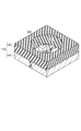
本発明の半導体素子搭載用基板は、底面及び壁面から構成される凹部を有し、凹部の底面が光半導体素子搭載部であり、凹部の壁面の少なくとも一部が本発明の光反射用熱硬化性樹脂組成物の硬化物からなるものである。図1は、本発明の光半導体素子搭載用基板の一実施形態を示す斜視図である。光半導体素子搭載用基板110は、金属配線105と、リフレクター103とを備え、金属配線105とリフレクター103とから形成されたる凹部を有している。すなわち、凹部の底面は金属配線105から構成され、凹部の壁面はリフレクター103から構成されるものであり、リフレクター103は、本発明の光反射用熱硬化性樹脂組成物の硬化物からなる成形体である。
[Optical semiconductor device mounting substrate]
The substrate for mounting a semiconductor element of the present invention has a recess composed of a bottom surface and a wall surface, the bottom surface of the recess is an optical semiconductor element mounting portion, and at least a part of the wall surface of the recess is the thermosetting for light reflection of the present invention. It consists of the hardened | cured material of an adhesive resin composition. FIG. 1 is a perspective view showing an embodiment of a substrate for mounting an optical semiconductor element of the present invention. The optical semiconductor
本発明の光半導体素子搭載用基板の製造方法は特に限定されないが、例えば、本発明の光反射用熱硬化性樹脂組成物を用いたトランスファー成形により製造することができる。図2は、本発明の光半導体素子搭載用基板を製造する工程の一実施形態を示す概略図である。光半導体素子搭載用基板は、例えば、金属箔から打ち抜きやエッチング等の公知の方法により金属配線105を形成する工程(図2(a))、次いで、該金属配線105を所定形状の金型151に配置し、金型151の樹脂注入口150から本発明の光反射用熱硬化性樹脂組成物を注入して、所定の条件でトランスファー成形する工程(図2(b))、そして、金型151を外し、形成された熱硬化性樹脂組成物の硬化物からなるリフレクター103に周囲を囲まれてなる光半導体素子搭載領域(凹部)200の所定位置に、電気めっきによりNi/銀めっき104を施す工程(図2(c))を経て製造することができる。なお、上記トランスファー成形の条件としては、金型温度170〜200℃、成形圧力0.5〜20MPaで60〜120秒間、アフターキュア温度120℃〜180℃で1〜3時間が好ましい。
Although the manufacturing method of the board | substrate for optical semiconductor element mounting of this invention is not specifically limited, For example, it can manufacture by transfer molding using the thermosetting resin composition for light reflections of this invention. FIG. 2 is a schematic view showing an embodiment of a process for producing an optical semiconductor element mounting substrate of the present invention. For the optical semiconductor element mounting substrate, for example, a step of forming the
[光半導体装置]
本発明の光半導体装置は、上記光半導体素子搭載用基板と、光半導体素子搭載用基板の凹部内に設けられた光半導体素子と、凹部を充填して光半導体素子を封止する封止樹脂部とを備えるものである。
[Optical semiconductor device]
An optical semiconductor device of the present invention includes the optical semiconductor element mounting substrate, an optical semiconductor element provided in a recess of the optical semiconductor element mounting substrate, and a sealing resin that fills the recess and seals the optical semiconductor element. Part.
図3は、本発明の光半導体素子搭載用基板110に光半導体素子100を搭載した状態の一実施形態を示す斜視図である。図3に示すように、光半導体素子100は、光半導体素子搭載用基板110の光半導体素子搭載領域(凹部)200の所定位置に搭載され、金属配線105とボンディングワイヤ102により電気的に接続される。図4及び5は、本発明の光半導体装置の一実施形態を示す模式断面図である。図4及び5に示すように、光半導体装置は、光半導体素子搭載用基板110と、光半導体素子搭載用基板110の凹部200内の所定位置に設けられた光半導体素子100と、凹部200を充填して光半導体素子を封止する蛍光体106を含む透明封止樹脂101からなる封止樹脂部とを備えており、光半導体素子100と金属配線105とがボンディングワイヤ102又ははんだバンプ107により電気的に接続されている。
FIG. 3 is a perspective view showing an embodiment in which the
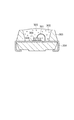
図6もまた、本発明の光半導体装置の一実施形態を示す模式断面図である。図6に示す光半導体装置では、リフレクター303が形成されたリード304上の所定位置にダイボンド材306を介してLED素子300が配置され、LED素子300とリード304とがボンディングワイヤ301により電気的に接続され、蛍光体305を含む透明封止樹脂302によりLED体素子300が封止されている。
FIG. 6 is also a schematic cross-sectional view showing an embodiment of the optical semiconductor device of the present invention. In the optical semiconductor device shown in FIG. 6, the
以上、本発明の好適な実施形態について説明したが、本発明はこれに制限されるものではない。 As mentioned above, although preferred embodiment of this invention was described, this invention is not restrict | limited to this.
以下に、本発明を実施例に基づいて具体的に説明するが、本発明はこれに限定されるものではない。 Hereinafter, the present invention will be specifically described based on examples, but the present invention is not limited thereto.
<被覆アルミナ粒子の作製>
アルミナ(アドマテックス社製、商品名「AO−802」、中心粒径1.0μm)100質量部及びテトラエトキシシラン(コルコート社製、商品名「TEOS28」)1.3質量部をプラスチック容器に入れ、ミックスロータで16時間混合した。次いで、上記混合物をガラス製容器に移し、オーブン中で100℃に加熱し、8時間乾燥し、無機酸化物層が形成された被覆アルミナ粒子を得た。
<Preparation of coated alumina particles>
100 parts by mass of alumina (manufactured by Admatechs, product name “AO-802”, center particle size 1.0 μm) and 1.3 parts by mass of tetraethoxysilane (manufactured by Colcoat, product name “TEOS28”) are put in a plastic container. And mixed for 16 hours in a mix rotor. Next, the mixture was transferred to a glass container, heated to 100 ° C. in an oven, and dried for 8 hours to obtain coated alumina particles on which an inorganic oxide layer was formed.
得られた被覆アルミナ粒子の中心粒径をBeckman Coulter社製、商品名「LS 13 320」を用いて測定したところ、0.28μmであった。また、赤外分光光度法により、得られた被覆アルミナ粒子の表面に二酸化ケイ素及びSi−OH基由来のシグナルが観られ、被覆アルミナ粒子の表面に二酸化ケイ素からなる薄膜が存在していることを確認した。さらに、得られた被覆アルミナ粒子の表面を電子顕微鏡で観察し、被覆アルミナ粒子が凝集していないことを確認した。 The center particle diameter of the obtained coated alumina particles was measured using a product name “LS 13 320” manufactured by Beckman Coulter, and found to be 0.28 μm. Further, by infrared spectrophotometry, signals derived from silicon dioxide and Si—OH groups were observed on the surface of the obtained coated alumina particles, and a thin film made of silicon dioxide was present on the surface of the coated alumina particles. confirmed. Furthermore, the surface of the obtained coated alumina particles was observed with an electron microscope, and it was confirmed that the coated alumina particles were not aggregated.
<光反射用熱硬化性樹脂組成物の作製>
(実施例1〜5)
上記被覆アルミナ粒子を用い、表1に示す配合量で各成分を配合し、ミキサーによって十分混練した後、ミキシングロールにより40℃で15分溶融混練し、冷却、粉砕を行い、実施例1〜5の光反射用熱硬化性樹脂組成物を作製した。なお、表中の各成分の配合量の単位は質量部を示す。
<Preparation of thermosetting resin composition for light reflection>
(Examples 1-5)
Using the above coated alumina particles, each component was blended in the blending amounts shown in Table 1, sufficiently kneaded with a mixer, then melt-kneaded with a mixing roll at 40 ° C. for 15 minutes, cooled and ground, and Examples 1 to 5 A thermosetting resin composition for light reflection was prepared. In addition, the unit of the compounding quantity of each component in a table | surface shows a mass part.
*1:トリスグリシジルイソシアヌレート(エポキシ当量100、日産化学社製、商品名:TEPIC−S)
*2:ヘキサヒドロ無水フタル酸(和光純薬工業社製)
*3:水素化トリメリット酸無水物(三菱ガス化学社製、商品名:H−TMAn)
*4:テトラ−n−ブチルホスホニウム−o,o−ジエチルホスホロジチエート(日本化学工業社製、商品名:PX−4ET)
*5:トリメトキシエポキシシラン(東レダウコーニング社製、商品名:A−187)
*6:脂肪酸エステル(クラリアント社製、商品名:ヘキストワックスE)
*7:脂肪族エーテル(東洋ペトロライト社製、商品名:ユニトックス420)
*8:溶融シリカ(電気化学工業社製、商品名:FB−301)
*9:中空粒子(住友3M社製、商品名:S60−HS:)
* 1: Trisglycidyl isocyanurate (epoxy equivalent 100, manufactured by Nissan Chemical Co., Ltd., trade name: TEPIC-S)
* 2: Hexahydrophthalic anhydride (manufactured by Wako Pure Chemical Industries, Ltd.)
* 3: Hydrogenated trimellitic anhydride (Mitsubishi Gas Chemical Co., Ltd., trade name: H-TMAn)
* 4: Tetra-n-butylphosphonium-o, o-diethyl phosphorodithioate (manufactured by Nippon Chemical Industry Co., Ltd., trade name: PX-4ET)
* 5: Trimethoxyepoxysilane (manufactured by Toray Dow Corning, trade name: A-187)
* 6: Fatty acid ester (manufactured by Clariant, trade name: Hoechst wax E)
* 7: Aliphatic ether (Toyo Petrolite, product name: Unitox 420)
* 8: Fused silica (manufactured by Denki Kagaku Kogyo, trade name: FB-301)
* 9: Hollow particles (manufactured by Sumitomo 3M, trade name: S60-HS :)
(比較例1〜5)
未処理のアルミナ(アドマテックス社製、商品名「AO−802」)を用い、表2に示す配合量で各成分を配合し、ミキサーによって十分混練した後、ミキシングロールにより40℃で15分溶融混練し、冷却、粉砕を行い、比較例1〜5の光反射用熱硬化性樹脂組成物を作製した。
(Comparative Examples 1-5)
Using untreated alumina (manufactured by Admatechs, trade name “AO-802”), each component was blended in the blending amounts shown in Table 2 and sufficiently kneaded with a mixer, and then melted at 40 ° C. for 15 minutes with a mixing roll. It knead | mixed, cooled and grind | pulverized, and produced the thermosetting resin composition for light reflections of Comparative Examples 1-5.
<光反射用熱硬化性樹脂組成物の評価>
(熱時硬度の測定)
実施例1〜5及び比較例1〜5で得られた光反射用熱硬化性樹脂組成物を、成形金型温度180℃、成形圧力6.9MPa及び硬化時間90秒の条件で、それぞれトランスファー成形した。成形金型から取り出してから30秒後の成形品の硬度をショアD硬度計(ASTM D2240に準拠しショアDで測定した。)を用いて測定した。結果を表3に示す。
<Evaluation of thermosetting resin composition for light reflection>
(Measurement of hot hardness)
The light-reflective thermosetting resin compositions obtained in Examples 1 to 5 and Comparative Examples 1 to 5 were each formed by transfer molding under conditions of a molding die temperature of 180 ° C., a molding pressure of 6.9 MPa, and a curing time of 90 seconds. did. The hardness of the molded product 30 seconds after taking out from the molding die was measured using a Shore D hardness meter (measured with Shore D according to ASTM D2240). The results are shown in Table 3.
(離型性の評価)
実施例1〜5及び比較例1〜5で得られた光反射用熱硬化性樹脂組成物を、上述の条件で、それぞれトランスファー成形した後、成形温度を保ったまま金型から成形物を離型する際にカル、スプルー、ランナー、ゲート、キャビティーのいずれかの箇所で成形物に破壊が生じるか否かを目視で確認した。同様の操作を各光反射用熱硬化性樹脂組成物について、10回を行った。結果を表3に示す。
(Evaluation of releasability)
After the light-reflective thermosetting resin compositions obtained in Examples 1 to 5 and Comparative Examples 1 to 5 were respectively transfer molded under the above-described conditions, the molded product was separated from the mold while maintaining the molding temperature. When molding, it was visually confirmed whether or not the molded product was broken at any of the locations of the cull, sprue, runner, gate, and cavity. The same operation was performed 10 times for each light-reflective thermosetting resin composition. The results are shown in Table 3.
(光反射率の測定)
実施例1〜5及び比較例1〜5で得られた光反射用熱硬化性樹脂組成物を上述の条件でトランスファー成型した後、150℃で2時間ポストキュアして、厚み1.0mmのテストピースを作製した。積分球型分光光度計V−750型(日本分光株式会社製、商品名)を用いて、波長460nmにおける上記テストピースの初期光学反射率(光反射率)を測定した。結果を表3に示す。
(Measurement of light reflectance)
After the light-reflective thermosetting resin compositions obtained in Examples 1 to 5 and Comparative Examples 1 to 5 were transfer molded under the above-mentioned conditions, they were post-cured at 150 ° C. for 2 hours, and a thickness of 1.0 mm was tested. Pieces were made. The initial optical reflectivity (light reflectivity) of the test piece at a wavelength of 460 nm was measured using an integrating sphere spectrophotometer V-750 type (trade name, manufactured by JASCO Corporation). The results are shown in Table 3.
表3に示したように、実施例1〜5で得られた光反射用熱硬化性樹脂組成物は、いずれも成形直後の熱時硬度が高く、硬化促進剤の添加量によらず成形金型からの離型時に成形物が破壊されることはなかった。これに対して、比較例1〜5で得られた光反射用熱硬化性樹脂組成物は、熱時硬度が80未満と低く、成形金型からの離型時に成形物が破壊する場合があり、硬化促進剤の量が少なくなると成形物の破壊が増大した。これは、硬化阻害によるものであり、破壊モードは凝集破壊であった。以上のように、無機酸化物で被覆されたアルミナ粒子を配合することによって、アルミナ表面に存在するアルミニウムカチオンの影響を抑制し、成形性、硬化性に優れた光反射用熱硬化性樹脂組成物を製造できることが確認された。 As shown in Table 3, all of the thermoreflective resin compositions for light reflection obtained in Examples 1 to 5 have high heat hardness immediately after molding, and the molding metal is independent of the amount of curing accelerator added. The molded product was not destroyed when released from the mold. On the other hand, the light-reflective thermosetting resin compositions obtained in Comparative Examples 1 to 5 have a thermal hardness as low as less than 80, and the molded product may be destroyed when released from the molding die. When the amount of the curing accelerator decreases, the destruction of the molded product increases. This was due to inhibition of curing, and the failure mode was cohesive failure. As described above, by incorporating alumina particles coated with inorganic oxide, the influence of aluminum cations existing on the alumina surface is suppressed, and the thermosetting resin composition for light reflection excellent in moldability and curability. It was confirmed that can be manufactured.
100…光半導体素子、101…透明封止樹脂、102…ボンディングワイヤ、103…光反射用熱硬化性樹脂組成物の硬化物(リフレクター)、104…Ni/Agめっき、105…金属配線、106…蛍光体、107…はんだバンプ、110…光半導体素子搭載用基板、150…樹脂注入口、151…金型、200…光半導体素子搭載領域、300…LED素子、301…ワイヤボンド、302…透明封止樹脂、303…リフレクター、304…リード、305…蛍光体、306…ダイボンド材。
DESCRIPTION OF
Claims (13)
粒子状のアルミナ及び該アルミナの表面の少なくとも一部を覆う無機酸化物層を備える被覆アルミナ粒子と、
を含有する光反射用熱硬化性樹脂組成物。 A thermosetting resin containing an epoxy resin and a curing agent;
Coated alumina particles comprising particulate alumina and an inorganic oxide layer covering at least part of the surface of the alumina;
A thermosetting resin composition for light reflection, comprising:
前記凹部の底面が光半導体素子搭載部であり、前記凹部の壁面の少なくとも一部が請求項1〜10のいずれか一項に記載の光反射用熱硬化性樹脂組成物の硬化物からなる、光半導体素子搭載用基板。 Having a recess composed of a bottom surface and a wall surface;
The bottom surface of the recess is an optical semiconductor element mounting portion, and at least a part of the wall surface of the recess is made of a cured product of the thermosetting resin composition for light reflection according to any one of claims 1 to 10. A substrate for mounting optical semiconductor elements.
前記凹部の壁面の少なくとも一部を、請求項1〜10のいずれか一項に記載の光反射用熱硬化性樹脂組成物を用いたトランスファー成形により形成する工程を備える、光半導体素子搭載用基板の製造方法。 A method of manufacturing a substrate for mounting an optical semiconductor element having a recess composed of a bottom surface and a wall surface,
A substrate for mounting an optical semiconductor element, comprising a step of forming at least a part of the wall surface of the concave portion by transfer molding using the thermosetting resin composition for light reflection according to any one of claims 1 to 10. Manufacturing method.
前記光半導体素子搭載用基板の凹部内に設けられた光半導体素子と、
前記凹部を充填して前記光半導体素子を封止する封止樹脂部と、
を備え、
前記凹部の壁面の少なくとも一部が、請求項1〜10のいずれか一項に記載の光反射用熱硬化性樹脂組成物の硬化物からなる、光半導体装置。
An optical semiconductor element mounting substrate having a recess composed of a bottom surface and a wall surface;
An optical semiconductor element provided in a recess of the optical semiconductor element mounting substrate;
A sealing resin portion that fills the recess and seals the optical semiconductor element;
With
The optical semiconductor device in which at least one part of the wall surface of the said recessed part consists of hardened | cured material of the thermosetting resin composition for light reflections as described in any one of Claims 1-10.
Priority Applications (1)
| Application Number | Priority Date | Filing Date | Title |
|---|---|---|---|
| JP2008304642A JP2009246334A (en) | 2008-03-12 | 2008-11-28 | Thermosetting resin composition for light reflection, substrate for loading photosemiconductor device and manufacturing method therefor, and photosemiconductor device |
Applications Claiming Priority (2)
| Application Number | Priority Date | Filing Date | Title |
|---|---|---|---|
| JP2008062574 | 2008-03-12 | ||
| JP2008304642A JP2009246334A (en) | 2008-03-12 | 2008-11-28 | Thermosetting resin composition for light reflection, substrate for loading photosemiconductor device and manufacturing method therefor, and photosemiconductor device |
Publications (2)
| Publication Number | Publication Date |
|---|---|
| JP2009246334A true JP2009246334A (en) | 2009-10-22 |
| JP2009246334A5 JP2009246334A5 (en) | 2011-12-01 |
Family
ID=41307872
Family Applications (1)
| Application Number | Title | Priority Date | Filing Date |
|---|---|---|---|
| JP2008304642A Pending JP2009246334A (en) | 2008-03-12 | 2008-11-28 | Thermosetting resin composition for light reflection, substrate for loading photosemiconductor device and manufacturing method therefor, and photosemiconductor device |
Country Status (1)
| Country | Link |
|---|---|
| JP (1) | JP2009246334A (en) |
Cited By (6)
| Publication number | Priority date | Publication date | Assignee | Title |
|---|---|---|---|---|
| JP2011249786A (en) * | 2010-04-28 | 2011-12-08 | Mitsubishi Chemicals Corp | Package for semiconductor light emitting device and light emitting device |
| JP2012049519A (en) * | 2010-07-26 | 2012-03-08 | Mitsubishi Chemicals Corp | Package for semiconductor light-emitting device, and light-emitting device |
| JP2012049505A (en) * | 2010-07-30 | 2012-03-08 | Mitsubishi Chemicals Corp | Package for semiconductor light-emitting device and semiconductor light-emitting device |
| US8338845B2 (en) | 2010-01-29 | 2012-12-25 | Kabushiki Kaisha Toshiba | LED package and method for manufacturing the same |
| JP2014517518A (en) * | 2011-05-19 | 2014-07-17 | 晶能光電(江西)有限公司 | Production method and manufacturing method of gallium nitride base film chip |
| JP2020181924A (en) * | 2019-04-26 | 2020-11-05 | 日亜化学工業株式会社 | Manufacturing method of light-emitting device |
Citations (3)
| Publication number | Priority date | Publication date | Assignee | Title |
|---|---|---|---|---|
| JPH07316459A (en) * | 1994-05-25 | 1995-12-05 | Shin Etsu Chem Co Ltd | Production of surface-treated alumina |
| JP2006140207A (en) * | 2004-11-10 | 2006-06-01 | Hitachi Chem Co Ltd | Thermosetting resin composition for light reflection, optical semiconductor loading substrate using the same, its manufacturing method and optical semiconductor device |
| JP2007297601A (en) * | 2006-04-06 | 2007-11-15 | Hitachi Chem Co Ltd | Thermosetting resin composition for light reflection, substrate for loading photosemiconductor device using the same, method for producing the same, and photosemiconductor device |
-
2008
- 2008-11-28 JP JP2008304642A patent/JP2009246334A/en active Pending
Patent Citations (3)
| Publication number | Priority date | Publication date | Assignee | Title |
|---|---|---|---|---|
| JPH07316459A (en) * | 1994-05-25 | 1995-12-05 | Shin Etsu Chem Co Ltd | Production of surface-treated alumina |
| JP2006140207A (en) * | 2004-11-10 | 2006-06-01 | Hitachi Chem Co Ltd | Thermosetting resin composition for light reflection, optical semiconductor loading substrate using the same, its manufacturing method and optical semiconductor device |
| JP2007297601A (en) * | 2006-04-06 | 2007-11-15 | Hitachi Chem Co Ltd | Thermosetting resin composition for light reflection, substrate for loading photosemiconductor device using the same, method for producing the same, and photosemiconductor device |
Cited By (7)
| Publication number | Priority date | Publication date | Assignee | Title |
|---|---|---|---|---|
| US8338845B2 (en) | 2010-01-29 | 2012-12-25 | Kabushiki Kaisha Toshiba | LED package and method for manufacturing the same |
| JP2011249786A (en) * | 2010-04-28 | 2011-12-08 | Mitsubishi Chemicals Corp | Package for semiconductor light emitting device and light emitting device |
| JP2012049519A (en) * | 2010-07-26 | 2012-03-08 | Mitsubishi Chemicals Corp | Package for semiconductor light-emitting device, and light-emitting device |
| JP2012049505A (en) * | 2010-07-30 | 2012-03-08 | Mitsubishi Chemicals Corp | Package for semiconductor light-emitting device and semiconductor light-emitting device |
| JP2014517518A (en) * | 2011-05-19 | 2014-07-17 | 晶能光電(江西)有限公司 | Production method and manufacturing method of gallium nitride base film chip |
| JP2020181924A (en) * | 2019-04-26 | 2020-11-05 | 日亜化学工業株式会社 | Manufacturing method of light-emitting device |
| JP7256382B2 (en) | 2019-04-26 | 2023-04-12 | 日亜化学工業株式会社 | Method for manufacturing light emitting device |
Similar Documents
| Publication | Publication Date | Title |
|---|---|---|
| JP6306652B2 (en) | Thermosetting light reflecting resin composition and method for producing the same | |
| JP6365606B2 (en) | Thermosetting light reflecting resin composition, optical semiconductor element mounting substrate and optical semiconductor device using the resin composition | |
| JP5298468B2 (en) | Thermosetting light reflecting resin composition, substrate for mounting optical semiconductor element using the same, method for manufacturing the same, and optical semiconductor device | |
| JP5599561B2 (en) | Thermosetting resin composition, optical semiconductor element mounting substrate using the same, method for producing the same, and optical semiconductor device | |
| JP5672318B2 (en) | Manufacturing method of optical semiconductor device | |
| JP6096090B2 (en) | Thermosetting resin composition, optical semiconductor element mounting substrate using the same, method for producing the same, and optical semiconductor device | |
| JP2010242095A (en) | Thermosetting molding material | |
| JP5233186B2 (en) | Thermosetting light reflecting resin composition, substrate for mounting optical semiconductor element using the same, method for manufacturing the same, and optical semiconductor device | |
| JP2009246334A (en) | Thermosetting resin composition for light reflection, substrate for loading photosemiconductor device and manufacturing method therefor, and photosemiconductor device | |
| JP5936804B2 (en) | Thermosetting resin composition, substrate for mounting optical semiconductor element, manufacturing method thereof, and optical semiconductor device | |
| JP5803883B2 (en) | Optical semiconductor element mounting substrate, manufacturing method thereof, and optical semiconductor device | |
| JP5401907B2 (en) | Method for manufacturing thermosetting resin composition, substrate for mounting optical semiconductor element, method for manufacturing the same, and optical semiconductor device | |
| JP2015017271A (en) | Thermosetting resin composition, substrate for mounting optical semiconductor element and method for manufacturing the same, and optical semiconductor device |
Legal Events
| Date | Code | Title | Description |
|---|---|---|---|
| A521 | Written amendment |
Free format text: JAPANESE INTERMEDIATE CODE: A523 Effective date: 20111013 |
|
| A621 | Written request for application examination |
Free format text: JAPANESE INTERMEDIATE CODE: A621 Effective date: 20111013 |
|
| A131 | Notification of reasons for refusal |
Free format text: JAPANESE INTERMEDIATE CODE: A131 Effective date: 20121113 |
|
| A977 | Report on retrieval |
Free format text: JAPANESE INTERMEDIATE CODE: A971007 Effective date: 20121114 |
|
| A02 | Decision of refusal |
Free format text: JAPANESE INTERMEDIATE CODE: A02 Effective date: 20130312 |