JP2009246332A - Method of forming fine pattern of semiconductor device - Google Patents
Method of forming fine pattern of semiconductor device Download PDFInfo
- Publication number
- JP2009246332A JP2009246332A JP2008261675A JP2008261675A JP2009246332A JP 2009246332 A JP2009246332 A JP 2009246332A JP 2008261675 A JP2008261675 A JP 2008261675A JP 2008261675 A JP2008261675 A JP 2008261675A JP 2009246332 A JP2009246332 A JP 2009246332A
- Authority
- JP
- Japan
- Prior art keywords
- pattern
- region
- fine
- hard mask
- forming
- Prior art date
- Legal status (The legal status is an assumption and is not a legal conclusion. Google has not performed a legal analysis and makes no representation as to the accuracy of the status listed.)
- Granted
Links
Images


Classifications
-
- H—ELECTRICITY
- H01—ELECTRIC ELEMENTS
- H01L—SEMICONDUCTOR DEVICES NOT COVERED BY CLASS H10
- H01L21/00—Processes or apparatus adapted for the manufacture or treatment of semiconductor or solid state devices or of parts thereof
- H01L21/02—Manufacture or treatment of semiconductor devices or of parts thereof
- H01L21/02104—Forming layers
- H01L21/02107—Forming insulating materials on a substrate
- H01L21/02109—Forming insulating materials on a substrate characterised by the type of layer, e.g. type of material, porous/non-porous, pre-cursors, mixtures or laminates
- H01L21/02112—Forming insulating materials on a substrate characterised by the type of layer, e.g. type of material, porous/non-porous, pre-cursors, mixtures or laminates characterised by the material of the layer
- H01L21/02118—Forming insulating materials on a substrate characterised by the type of layer, e.g. type of material, porous/non-porous, pre-cursors, mixtures or laminates characterised by the material of the layer carbon based polymeric organic or inorganic material, e.g. polyimides, poly cyclobutene or PVC
-
- H—ELECTRICITY
- H01—ELECTRIC ELEMENTS
- H01L—SEMICONDUCTOR DEVICES NOT COVERED BY CLASS H10
- H01L21/00—Processes or apparatus adapted for the manufacture or treatment of semiconductor or solid state devices or of parts thereof
- H01L21/02—Manufacture or treatment of semiconductor devices or of parts thereof
- H01L21/04—Manufacture or treatment of semiconductor devices or of parts thereof the devices having at least one potential-jump barrier or surface barrier, e.g. PN junction, depletion layer or carrier concentration layer
- H01L21/18—Manufacture or treatment of semiconductor devices or of parts thereof the devices having at least one potential-jump barrier or surface barrier, e.g. PN junction, depletion layer or carrier concentration layer the devices having semiconductor bodies comprising elements of Group IV of the Periodic System or AIIIBV compounds with or without impurities, e.g. doping materials
- H01L21/30—Treatment of semiconductor bodies using processes or apparatus not provided for in groups H01L21/20 - H01L21/26
- H01L21/302—Treatment of semiconductor bodies using processes or apparatus not provided for in groups H01L21/20 - H01L21/26 to change their surface-physical characteristics or shape, e.g. etching, polishing, cutting
- H01L21/306—Chemical or electrical treatment, e.g. electrolytic etching
- H01L21/308—Chemical or electrical treatment, e.g. electrolytic etching using masks
-
- H—ELECTRICITY
- H01—ELECTRIC ELEMENTS
- H01L—SEMICONDUCTOR DEVICES NOT COVERED BY CLASS H10
- H01L21/00—Processes or apparatus adapted for the manufacture or treatment of semiconductor or solid state devices or of parts thereof
- H01L21/02—Manufacture or treatment of semiconductor devices or of parts thereof
- H01L21/02104—Forming layers
- H01L21/02107—Forming insulating materials on a substrate
- H01L21/02225—Forming insulating materials on a substrate characterised by the process for the formation of the insulating layer
- H01L21/0226—Forming insulating materials on a substrate characterised by the process for the formation of the insulating layer formation by a deposition process
- H01L21/02282—Forming insulating materials on a substrate characterised by the process for the formation of the insulating layer formation by a deposition process liquid deposition, e.g. spin-coating, sol-gel techniques, spray coating
-
- H—ELECTRICITY
- H01—ELECTRIC ELEMENTS
- H01L—SEMICONDUCTOR DEVICES NOT COVERED BY CLASS H10
- H01L21/00—Processes or apparatus adapted for the manufacture or treatment of semiconductor or solid state devices or of parts thereof
- H01L21/02—Manufacture or treatment of semiconductor devices or of parts thereof
- H01L21/027—Making masks on semiconductor bodies for further photolithographic processing not provided for in group H01L21/18 or H01L21/34
- H01L21/033—Making masks on semiconductor bodies for further photolithographic processing not provided for in group H01L21/18 or H01L21/34 comprising inorganic layers
- H01L21/0334—Making masks on semiconductor bodies for further photolithographic processing not provided for in group H01L21/18 or H01L21/34 comprising inorganic layers characterised by their size, orientation, disposition, behaviour, shape, in horizontal or vertical plane
- H01L21/0337—Making masks on semiconductor bodies for further photolithographic processing not provided for in group H01L21/18 or H01L21/34 comprising inorganic layers characterised by their size, orientation, disposition, behaviour, shape, in horizontal or vertical plane characterised by the process involved to create the mask, e.g. lift-off masks, sidewalls, or to modify the mask, e.g. pre-treatment, post-treatment
-
- H—ELECTRICITY
- H01—ELECTRIC ELEMENTS
- H01L—SEMICONDUCTOR DEVICES NOT COVERED BY CLASS H10
- H01L21/00—Processes or apparatus adapted for the manufacture or treatment of semiconductor or solid state devices or of parts thereof
- H01L21/02—Manufacture or treatment of semiconductor devices or of parts thereof
- H01L21/04—Manufacture or treatment of semiconductor devices or of parts thereof the devices having at least one potential-jump barrier or surface barrier, e.g. PN junction, depletion layer or carrier concentration layer
- H01L21/18—Manufacture or treatment of semiconductor devices or of parts thereof the devices having at least one potential-jump barrier or surface barrier, e.g. PN junction, depletion layer or carrier concentration layer the devices having semiconductor bodies comprising elements of Group IV of the Periodic System or AIIIBV compounds with or without impurities, e.g. doping materials
- H01L21/30—Treatment of semiconductor bodies using processes or apparatus not provided for in groups H01L21/20 - H01L21/26
- H01L21/302—Treatment of semiconductor bodies using processes or apparatus not provided for in groups H01L21/20 - H01L21/26 to change their surface-physical characteristics or shape, e.g. etching, polishing, cutting
- H01L21/306—Chemical or electrical treatment, e.g. electrolytic etching
- H01L21/308—Chemical or electrical treatment, e.g. electrolytic etching using masks
- H01L21/3083—Chemical or electrical treatment, e.g. electrolytic etching using masks characterised by their size, orientation, disposition, behaviour, shape, in horizontal or vertical plane
- H01L21/3086—Chemical or electrical treatment, e.g. electrolytic etching using masks characterised by their size, orientation, disposition, behaviour, shape, in horizontal or vertical plane characterised by the process involved to create the mask, e.g. lift-off masks, sidewalls, or to modify the mask, e.g. pre-treatment, post-treatment
-
- H—ELECTRICITY
- H01—ELECTRIC ELEMENTS
- H01L—SEMICONDUCTOR DEVICES NOT COVERED BY CLASS H10
- H01L21/00—Processes or apparatus adapted for the manufacture or treatment of semiconductor or solid state devices or of parts thereof
- H01L21/02—Manufacture or treatment of semiconductor devices or of parts thereof
- H01L21/04—Manufacture or treatment of semiconductor devices or of parts thereof the devices having at least one potential-jump barrier or surface barrier, e.g. PN junction, depletion layer or carrier concentration layer
- H01L21/18—Manufacture or treatment of semiconductor devices or of parts thereof the devices having at least one potential-jump barrier or surface barrier, e.g. PN junction, depletion layer or carrier concentration layer the devices having semiconductor bodies comprising elements of Group IV of the Periodic System or AIIIBV compounds with or without impurities, e.g. doping materials
- H01L21/30—Treatment of semiconductor bodies using processes or apparatus not provided for in groups H01L21/20 - H01L21/26
- H01L21/31—Treatment of semiconductor bodies using processes or apparatus not provided for in groups H01L21/20 - H01L21/26 to form insulating layers thereon, e.g. for masking or by using photolithographic techniques; After treatment of these layers; Selection of materials for these layers
- H01L21/3105—After-treatment
- H01L21/31058—After-treatment of organic layers
-
- H—ELECTRICITY
- H01—ELECTRIC ELEMENTS
- H01L—SEMICONDUCTOR DEVICES NOT COVERED BY CLASS H10
- H01L21/00—Processes or apparatus adapted for the manufacture or treatment of semiconductor or solid state devices or of parts thereof
- H01L21/02—Manufacture or treatment of semiconductor devices or of parts thereof
- H01L21/04—Manufacture or treatment of semiconductor devices or of parts thereof the devices having at least one potential-jump barrier or surface barrier, e.g. PN junction, depletion layer or carrier concentration layer
- H01L21/18—Manufacture or treatment of semiconductor devices or of parts thereof the devices having at least one potential-jump barrier or surface barrier, e.g. PN junction, depletion layer or carrier concentration layer the devices having semiconductor bodies comprising elements of Group IV of the Periodic System or AIIIBV compounds with or without impurities, e.g. doping materials
- H01L21/30—Treatment of semiconductor bodies using processes or apparatus not provided for in groups H01L21/20 - H01L21/26
- H01L21/31—Treatment of semiconductor bodies using processes or apparatus not provided for in groups H01L21/20 - H01L21/26 to form insulating layers thereon, e.g. for masking or by using photolithographic techniques; After treatment of these layers; Selection of materials for these layers
- H01L21/312—Organic layers, e.g. photoresist
-
- H—ELECTRICITY
- H01—ELECTRIC ELEMENTS
- H01L—SEMICONDUCTOR DEVICES NOT COVERED BY CLASS H10
- H01L21/00—Processes or apparatus adapted for the manufacture or treatment of semiconductor or solid state devices or of parts thereof
- H01L21/02—Manufacture or treatment of semiconductor devices or of parts thereof
- H01L21/04—Manufacture or treatment of semiconductor devices or of parts thereof the devices having at least one potential-jump barrier or surface barrier, e.g. PN junction, depletion layer or carrier concentration layer
- H01L21/18—Manufacture or treatment of semiconductor devices or of parts thereof the devices having at least one potential-jump barrier or surface barrier, e.g. PN junction, depletion layer or carrier concentration layer the devices having semiconductor bodies comprising elements of Group IV of the Periodic System or AIIIBV compounds with or without impurities, e.g. doping materials
- H01L21/30—Treatment of semiconductor bodies using processes or apparatus not provided for in groups H01L21/20 - H01L21/26
- H01L21/31—Treatment of semiconductor bodies using processes or apparatus not provided for in groups H01L21/20 - H01L21/26 to form insulating layers thereon, e.g. for masking or by using photolithographic techniques; After treatment of these layers; Selection of materials for these layers
- H01L21/3205—Deposition of non-insulating-, e.g. conductive- or resistive-, layers on insulating layers; After-treatment of these layers
- H01L21/321—After treatment
- H01L21/3213—Physical or chemical etching of the layers, e.g. to produce a patterned layer from a pre-deposited extensive layer
- H01L21/32139—Physical or chemical etching of the layers, e.g. to produce a patterned layer from a pre-deposited extensive layer using masks
-
- H—ELECTRICITY
- H01—ELECTRIC ELEMENTS
- H01L—SEMICONDUCTOR DEVICES NOT COVERED BY CLASS H10
- H01L27/00—Devices consisting of a plurality of semiconductor or other solid-state components formed in or on a common substrate
- H01L27/02—Devices consisting of a plurality of semiconductor or other solid-state components formed in or on a common substrate including semiconductor components specially adapted for rectifying, oscillating, amplifying or switching and having at least one potential-jump barrier or surface barrier; including integrated passive circuit elements with at least one potential-jump barrier or surface barrier
- H01L27/04—Devices consisting of a plurality of semiconductor or other solid-state components formed in or on a common substrate including semiconductor components specially adapted for rectifying, oscillating, amplifying or switching and having at least one potential-jump barrier or surface barrier; including integrated passive circuit elements with at least one potential-jump barrier or surface barrier the substrate being a semiconductor body
- H01L27/10—Devices consisting of a plurality of semiconductor or other solid-state components formed in or on a common substrate including semiconductor components specially adapted for rectifying, oscillating, amplifying or switching and having at least one potential-jump barrier or surface barrier; including integrated passive circuit elements with at least one potential-jump barrier or surface barrier the substrate being a semiconductor body including a plurality of individual components in a repetitive configuration
- H01L27/105—Devices consisting of a plurality of semiconductor or other solid-state components formed in or on a common substrate including semiconductor components specially adapted for rectifying, oscillating, amplifying or switching and having at least one potential-jump barrier or surface barrier; including integrated passive circuit elements with at least one potential-jump barrier or surface barrier the substrate being a semiconductor body including a plurality of individual components in a repetitive configuration including field-effect components
-
- H—ELECTRICITY
- H10—SEMICONDUCTOR DEVICES; ELECTRIC SOLID-STATE DEVICES NOT OTHERWISE PROVIDED FOR
- H10B—ELECTRONIC MEMORY DEVICES
- H10B99/00—Subject matter not provided for in other groups of this subclass
Abstract
Description
本発明は、半導体素子の微細パターン形成方法に係り、特に、SARP(Self−Aligned Reverse Pattering)工程を利用して微細ピッチのハードマスクパターンを形成するに当たって、基板上の相異なる領域で相異なるパターン密度で微細パターンを形成するための半導体素子の微細パターン形成方法に関する。 The present invention relates to a method for forming a fine pattern of a semiconductor device, and more particularly, in forming a hard mask pattern with a fine pitch using a SARP (Self-Aligned Reverse Patterning) process, different patterns in different regions on a substrate. The present invention relates to a method for forming a fine pattern of a semiconductor device for forming a fine pattern with a density.
高集積化された半導体素子の製造時において、パターン微細化が必須である。狭い面積に多くの素子を集積させるためには、個別素子のサイズをなるべく小さく形成せねばならず、このためには形成しようとするパターンそれぞれの幅と前記パターン間の間隔との和であるピッチを小さくせねばならない。最近、半導体素子のデザインルールが急減するにつれて、半導体素子の具現に必要なパターンを形成するためのフォトリソグラフィ工程において、解像限界のために微細ピッチを持つパターンを形成するのに限界がある。特に、基板上にラインアンドスペースパターン(line and space pattern、以下、“L/Sパターン”という)の形成のためのフォトリソグラフィ工程時に、解像限界によって微細ピッチを持つ所望のパターンを形成するのに限界がある。 Pattern miniaturization is indispensable when manufacturing highly integrated semiconductor devices. In order to integrate a large number of elements in a small area, the size of each individual element must be made as small as possible. For this purpose, the pitch is the sum of the width of each pattern to be formed and the interval between the patterns. Must be reduced. Recently, as the design rules for semiconductor devices have rapidly decreased, there is a limit in forming a pattern having a fine pitch due to a resolution limit in a photolithography process for forming a pattern necessary for realizing the semiconductor device. In particular, a desired pattern having a fine pitch is formed by a resolution limit during a photolithography process for forming a line and space pattern (hereinafter referred to as “L / S pattern”) on a substrate. There is a limit.
前記のようなフォトリソグラフィ工程での解像限界を克服するために、微細ピッチを持つハードマスクパターンを形成するための多様な方法が提案された。
しかし、半導体基板上のセルアレイ領域のようにパターン密度が比較的高い領域と、周辺回路領域またはコア領域のようにパターン密度が比較的低い領域とで、相異なるパターン密度を持つ微細パターンを同時に形成するための新たな工程開発が要求される。
In order to overcome the resolution limit in the photolithography process as described above, various methods for forming a hard mask pattern having a fine pitch have been proposed.
However, fine patterns with different pattern densities are formed simultaneously in a relatively high pattern density region such as a cell array region on a semiconductor substrate and a relatively low pattern density region such as a peripheral circuit region or a core region. New process development is required.
本発明の目的は、フォトリソグラフィ工程での解像限界を克服できる微細ピッチのパターンを具現するに当たって、同じ基板上にパターン密度、またはパターン幅の異なる多様なサイズ及び多様なピッチのパターンを同時に形成できる半導体素子の微細パターン形成方法を提供することである。 It is an object of the present invention to simultaneously form patterns of various sizes and various pitches having different pattern densities or pattern widths on the same substrate in realizing a fine pitch pattern capable of overcoming the resolution limit in the photolithography process. Another object is to provide a method for forming a fine pattern of a semiconductor device.
前記目的を達成するために、本発明による半導体素子の微細パターン形成方法では、第1領域及び第2領域を備える基板上に、前記第1領域及び前記第2領域のうち、前記第1領域のみに第1ピッチで反復配置される複数のモールドパターンを形成するステップと、前記第1領域で前記モールドパターンを覆う微細マスク層を、前記基板上の第1領域及び第2領域に同時に形成するステップと、前記第1領域及び前記第2領域のうち、前記第2領域のみに前記微細マスク層の上面のうち一部を覆う上部ハードマスクパターンを形成するステップと、前記上部ハードマスクパターンをエッチングマスクとして、前記第1領域及び前記第2領域で前記微細マスク層をエッチングし、前記第1領域には、前記微細マスク層の第1部分で形成される複数の微細スペーサを前記複数のモールドパターンそれぞれの両側壁に形成すると同時に、前記第2領域には前記微細マスク層の第2部分で形成される低密度マスクパターンを形成するステップと、を含む。 In order to achieve the above object, in the method for forming a fine pattern of a semiconductor device according to the present invention, only the first region of the first region and the second region is formed on a substrate including the first region and the second region. Forming a plurality of mold patterns repeatedly arranged at a first pitch, and simultaneously forming a fine mask layer covering the mold pattern in the first region in the first region and the second region on the substrate. Forming an upper hard mask pattern that covers a part of the upper surface of the fine mask layer only in the second region of the first region and the second region; and etching the upper hard mask pattern into an etching mask. As a result, the fine mask layer is etched in the first region and the second region, and the first region includes a plurality of portions formed by the first portion of the fine mask layer. At the same time the fine spacers are formed on both side walls of each of the plurality of mold patterns, the second region and forming a low-density mask pattern formed of a second portion of the fine mask layer.
前記基板は被エッチング膜を備え、前記複数のモールドパターン及び前記微細マスク層はそれぞれ前記被エッチング膜上に形成され、前記複数の微細スペーサ及び低密度マスクパターンが形成された後、前記複数の微細スペーサ及び低密度マスクパターンをエッチングマスクとして、前記第1領域及び前記第2領域で前記被エッチング膜をエッチングするステップをさらに含む。 The substrate includes an etching target film, the plurality of mold patterns and the fine mask layer are respectively formed on the etching target film, and the plurality of fine spacers and the low density mask pattern are formed, and then the plurality of fine patterns are formed. The method further includes etching the film to be etched in the first region and the second region using the spacer and the low density mask pattern as an etching mask.
前記基板は、半導体基板と、前記半導体基板上に形成された下部ハードマスク層とを備え、前記複数のモールドパターン及び前記微細マスク層は、それぞれ前記下部ハードマスク層上に形成される。前記下部ハードマスク層は1種の物質からなる単一層、またはそれぞれ異なる物質からなる複数のハードマスク層が順次積層された多重層で形成される。 The substrate includes a semiconductor substrate and a lower hard mask layer formed on the semiconductor substrate, and the plurality of mold patterns and the fine mask layer are respectively formed on the lower hard mask layer. The lower hard mask layer may be a single layer made of one material or a multiple layer in which a plurality of hard mask layers made of different materials are sequentially stacked.
前記複数の微細スペーサ及び低密度マスクパターンが形成された後、前記複数の微細スペーサ及び前記低密度マスクパターンをエッチングマスクとして、前記第1領域及び前記第2領域で前記下部ハードマスク層を同時にエッチングして、前記第1領域及び前記第2領域でそれぞれ異なるパターン密度を持つ下部ハードマスクパターンを形成する。また、前記下部ハードマスクパターンが形成された後、前記下部ハードマスクパターンをエッチングマスクとして、前記第1領域及び前記第2領域で前記半導体基板をエッチングして、前記第1領域及び前記第2領域でそれぞれ異なる密度を持つ活性領域を同時に定義できる。 After the plurality of fine spacers and the low density mask pattern are formed, the lower hard mask layer is simultaneously etched in the first region and the second region using the plurality of fine spacers and the low density mask pattern as an etching mask. Then, lower hard mask patterns having different pattern densities are formed in the first region and the second region. In addition, after the lower hard mask pattern is formed, the semiconductor substrate is etched in the first region and the second region using the lower hard mask pattern as an etching mask, and the first region and the second region are etched. Can simultaneously define active regions with different densities.
前記複数のモールドパターンと前記上部ハードマスクパターンとは、同じ物質からなってもよく、相異なる物質からなってもよい。
前記上部ハードマスクパターンを形成するステップは、前記第1領域及び前記第2領域で前記微細マスク層上に上部ハードマスク層を形成するステップと、前記第1領域及び前記第2領域のうち、前記第2領域のみに前記上部ハードマスク層の上面のうち一部を覆うマスクパターンを形成するステップと、前記マスクパターンをエッチングマスクとして、前記上部ハードマスク層をエッチングして前記上部ハードマスクパターンを形成するステップと、を含む。
The plurality of mold patterns and the upper hard mask pattern may be made of the same material or different materials.
The step of forming the upper hard mask pattern includes forming an upper hard mask layer on the fine mask layer in the first region and the second region, and out of the first region and the second region, Forming a mask pattern covering a part of the upper surface of the upper hard mask layer only in the second region; and etching the upper hard mask layer using the mask pattern as an etching mask to form the upper hard mask pattern Including the steps of:
本発明による半導体素子の微細パターン形成方法で、前記複数の微細スペーサ及び低密度マスクパターンが形成された後、前記複数のモールドパターン及び前記上部ハードマスクパターンを除去するステップをさらに含む。前記複数のモールドパターン及び前記上部ハードマスクパターンは、同時に除去されてもよく、順次除去されてもよい。 The method for forming a fine pattern of a semiconductor device according to the present invention further comprises removing the plurality of mold patterns and the upper hard mask pattern after the plurality of fine spacers and the low density mask pattern are formed. The plurality of mold patterns and the upper hard mask pattern may be removed simultaneously or sequentially.
本発明による半導体素子の微細パターン形成方法によれば、基板上の相異なる領域で相異なるパターン密度を持つ微細マスクパターンを同時に形成した後、これをエッチングマスクとして利用して前記基板上の相異なる領域に相異なる密度を持つパターンを同時に形成する。したがって、基板上で形成しようとする単位素子の種類及び密度によって基板に多様な幅及び多様なピッチを持つ微細パターンを、単純化された工程により形成できる。特に、高密度パターン領域に具現しようとする微細パターンを形成するに当たって、フォトリソグラフィ工程での解像限界を克服できる微細ピッチのパターンを容易に形成でき、このような微細ピッチのパターンを形成する時に、高密度パターン領域での微細パターン形成工程を低密度パターン領域でのパターン形成工程と同時に進めることによって、同一層上に低密度パターン及び高密度パターンを同時に具現できる。したがって、高集積半導体素子の製造工程が単純化され、低コストになって製品競争力を向上させることができる。 According to the method for forming a fine pattern of a semiconductor device according to the present invention, a fine mask pattern having a different pattern density is simultaneously formed in different regions on the substrate, and then different from each other on the substrate by using this as an etching mask. Patterns having different densities are simultaneously formed in the region. Therefore, fine patterns having various widths and various pitches can be formed on the substrate by a simplified process according to the type and density of unit elements to be formed on the substrate. In particular, when forming a fine pattern to be embodied in a high-density pattern region, it is possible to easily form a fine pitch pattern that can overcome the resolution limit in the photolithography process, and when forming such a fine pitch pattern. By performing the fine pattern forming process in the high density pattern region simultaneously with the pattern forming process in the low density pattern region, the low density pattern and the high density pattern can be simultaneously realized on the same layer. Therefore, the manufacturing process of the highly integrated semiconductor device is simplified, the cost is reduced, and the product competitiveness can be improved.
次いで、本発明の望ましい実施形態について添付図面を参照して詳細に説明する。しかし、本発明の実施形態はいろいろな形態に変形でき、本発明の範囲が後述する実施形態に限定されると解釈されてはならない。図面で、層及び領域の厚さは明細書の明確性のために誇張されている。図面上で同じ符号は同じ要素を称する。 Next, preferred embodiments of the present invention will be described in detail with reference to the accompanying drawings. However, the embodiments of the present invention can be modified in various forms, and the scope of the present invention should not be construed to be limited to the embodiments described below. In the drawings, the thickness of layers and regions are exaggerated for clarity. Like reference numerals refer to like elements throughout the drawings.
(第1実施形態)
図1Aから図1Kは、本発明の第1実施形態による半導体素子の微細パターン形成方法を説明するために工程順序によって示した断面図である。
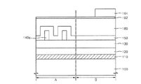
図1Aを参照すれば、基板100上に被エッチング膜110を形成し、被エッチング膜110上に下部ハードマスク層120、130を形成する。
本実施形態においては、下部ハードマスク層120、130は、第1ハードマスク層120及び第2ハードマスク層130が順次積層された二重層構造を持つ。しかし、本発明はこれに限定されるものではない。例えば、下部マスク層は1種の物質からなる単一層、またはそれぞれ異なる物質からなる複数のハードマスク層が順次積層された多重層で形成されることもある。
(First embodiment)
1A to 1K are cross-sectional views illustrating a method for forming a fine pattern of a semiconductor device according to a first embodiment of the present invention according to a process order.
Referring to FIG. 1A, a film to be etched 110 is formed on the
In the present embodiment, the lower
基板100は、高密度パターン領域A及び低密度パターン領域Bを備える。高密度パターン領域Aは、例えば、半導体素子のセルアレイ領域のように単位面積当たりパターン密度が比較的高い領域である。低密度パターン領域Bは、単位面積当たりパターン密度が比較的低い領域であり、例えば、周辺回路領域またはコア領域、その中でも特に低電圧領域または高電圧領域でありうる。または、低密度パターン領域Bは、セルアレイ領域のうち形成しようとするパターンの密度が比較的低い領域でありうる。
The
基板100は、シリコン基板で形成されうる。
被エッチング膜110は、形成しようとするパターンの用途によって多様な物質からなりうる。基板100上にゲート電極を形成する場合には、被エッチング膜110は導電層、例えば、ドーピングされたポリシリコン層、またはドーピングされたポリシリコン層と金属シリサイド層との積層構造になりうる。そして、ビットラインを形成する場合には、被エッチング膜100は、金属、例えば、タングステンまたはアルミニウムからなりうる。被エッチング膜110が絶縁層である場合、例えば、TEOS(tetraethyl orthosilicate)、FSG(fluorine silicate glass)、SiOC、SiLKなどのように比較的低い誘電定数を持つ絶縁物質からなりうる。または、被エッチング膜110は、導電層と絶縁層との組み合わせで形成されうる。最終的に形成しようとする微細パターンが基板100のエッチングにより形成される場合には、被エッチング膜110は省略できる。例えば、基板100に活性領域を定義するために本発明による方法を利用する場合には、被エッチング膜110を省略できる。
The
The
第1ハードマスク層120及び第2ハードマスク層130は、それぞれ被エッチング膜110の材料、後続工程で第2ハードマスク層130上に形成される他のエッチングマスクの材料、及び形成しようとするパターンの用途によって、下部の被エッチング膜のエッチング時にエッチング耐性を持つことができる多様な物質からなりうる。第1ハードマスク層120及び第2ハードマスク層130は、所定のエッチング条件に対して相異なるエッチング選択比を持つ相異なる物質からなる。例えば、第1ハードマスク層120及び第2ハードマスク層130は、それぞれ酸化膜、窒化膜、及びポリシリコン膜で選択される相異なる膜で形成されうる。例えば、第1ハードマスク層120及び第2ハードマスク層130のうち一つは、熱酸化膜、CVD酸化膜、USG膜(Undoped Silicate Glassfilm)及びHDP酸化膜(High Density Plasma oxide film)からなる群から選択されるいずれか一つの酸化膜で形成されうる。または、第1ハードマスク層120及び第2ハードマスク層130のうち一つは、SiON、SiN、SiBN、BNのような窒化膜、またはポリシリコン膜で形成されうる。
The first
図1Bを参照すれば、第2ハードマスク層130上にモールド層140及び反射防止膜142を順次形成し、高密度パターン領域Aで、反射防止膜142上にフォトレジストパターン144を形成する。
モールド層140は、例えば、炭素含有膜、酸化膜、ポリシリコン膜、窒化膜、フォトレジスト膜、またはAl、Wのような金属膜で形成されうる。モールド層140が炭素含有膜で形成される場合、モールド層140を構成する炭素含有膜は、芳香族環を含む炭化水素化合物またはその誘導体からなる有機化合物で形成されうる。例えば、モールド層140を構成する炭素含有膜は、フェニル、ベンゼン、またはナフタレンのような芳香族環を含む有機化合物からなりうる。前記炭素含有膜は、モールド層140を構成する有機化合物の総重量を基準に約85〜99重量%の比較的高い炭素含有量を持つ膜で形成されうる。前記炭素含有膜は、例えば、スピンコーティングにより形成されうる。前記炭素含有膜を形成するための例示的な方法で、第2ハードマスク層130上に有機化合物を約1000〜5000Åの厚さでスピンコーティングした後、得られた有機化合物層を約150〜350℃の温度下で1次ベイクして前記炭素含有膜を形成する。前記1次ベイクは約60秒間行なわれうる。次いで、前記炭素含有膜を約300〜550℃の温度下で2次ベイクして硬化させる。前記2次ベイクは約30〜300秒間行なわれうる。このように、前記炭素含有膜を硬化させることによって、前記炭素含有膜上に他の膜質を形成する時に約400℃以上の比較的高温下で蒸着工程を行っても、蒸着工程中に前記炭素含有膜に悪影響が及ばなくなる。
Referring to FIG. 1B, a
The
反射防止膜142は、無機物または有機物からなりうる。例えば、反射防止膜142は、SiON膜またはBARC膜(Bottom Anti−Reflective Coating film)で形成されうる。
フォトレジストパターン144は、高密度パターン領域Aで最終的に形成しようとする微細パターンのピッチ(PA)より2倍大きいピッチ(2PA)を持つように形成できる。
The
The
図1Cを参照すれば、フォトレジストパターン144をエッチングマスクとして、反射防止膜142及びモールド層140をエッチングして複数のモールドパターン140aを形成する。次いで、モールドパターン140a上に残っている反射防止膜142及びフォトレジストパターン144を除去する。
Referring to FIG. 1C, the
高密度パターン領域Aで、複数のモールドパターン140aは、最終的に形成しようとする微細パターンのピッチ(PA)より2倍大きい第1ピッチ(2PA)を持つように形成できる。
図1Dを参照すれば、モールドパターン140a及び第2ハードマスク層130上に微細マスク層150を形成する。微細マスク層150は、高密度パターン領域Aでモールドパターン140aの上面及び側壁と第2ハードマスク層130の上面とを均一な厚さで覆うと同時に、低密度パターン領域Bで第2ハードマスク層130の上面を均一な厚さで覆うように形成される。
In the high-density pattern region A, the plurality of
Referring to FIG. 1D, a
微細マスク層150は、モールドパターン140a及び第2ハードマスク層130のエッチング時にエッチング耐性を持つことができる物質からなる。例えば、微細マスク層150は、ALD(Atomic Layer Deposition)工程により形成される酸化膜、または窒化膜で形成されうる。例えば、モールドパターン140aは、図1Bを参照して説明した炭素含有膜で形成され、微細マスク層150は、酸化膜で形成されうる。または、モールドパターン140aは酸化膜で形成され、微細マスク層150は窒化膜で形成されうる。
The
図1Eを参照すれば、基板100上の高密度パターン領域A及び低密度パターン領域Bに、それぞれ微細マスク層150を完全に覆う上部ハードマスク層160を形成する。次いで、上部ハードマスク層160上に反射防止膜162を形成し、高密度パターン領域Aに所定形状のフォトレジストパターン164を形成する。
Referring to FIG. 1E, an upper
フォトレジストパターン164は、低密度パターン領域Bで最終的に具現しようとするパターンと同じピッチ及び同じ形状を持つように形成できる。
反射防止膜162は無機物または有機物からなりうる。例えば、反射防止膜162は、SiON膜またはBARC膜からなりうる。
The
The
上部ハードマスク層160は、炭素含有膜、例えば、芳香族環を含む炭化水素化合物またはその誘導体からなる有機化合物を含む炭素含有膜で形成されうる。例えば、上部ハードマスク層160を構成する炭素含有膜は、フェニル、ベンゼン、またはナフタレンのような芳香族環を含む有機化合物からなりうる。前記炭素含有膜は、前記上部ハードマスク層160を構成する有機化合物の総重量を基準に約85〜99重量%の比較的高い炭素含有量を持つ膜で形成されうる。前記炭素含有膜は、例えば、スピンコーティングにより形成できる。前記炭素含有膜を形成するための例示的な方法で、前記微細マスク層150上に有機化合物を約1000〜5000Åの厚さでスピンコーティングした後、得られた有機化合物層を約150〜350℃の温度下で1次ベイクして前記炭素含有膜を形成する。前記1次ベイクは、約60秒間行なわれうる。次いで、前記炭素含有膜を約300〜550℃の温度下で2次ベイクして硬化させる。前記2次ベイクは、約30〜300秒間行なわれうる。このように、前記炭素含有膜を硬化させることによって、前記炭素含有膜上に他の膜質を形成するとき、約400℃以上の比較的高温下で蒸着工程を行っても、蒸着工程中に前記炭素含有膜に悪影響が及ばなくなる。
The upper
例示的な方法で、上部ハードマスク層160をモールドパターン140aと同じ物質で形成できる。上部ハードマスク層160を形成するために炭素含有膜をスピンコーティング工程で形成する場合、高密度パターン領域Aのうち、相互隣接した2個のモールドパターン140aの間で前記微細マスク層150の上面に形成された段差によって形成されるリセスの内部にも、上部ハードマスク層160がボイドなしによく満たされうる。
In an exemplary method, the upper
図1Fを参照すれば、フォトレジストパターン164をエッチングマスクとして、反射防止膜162及び上部ハードマスク層160を異方性ドライエッチングして、低密度パターン領域Bに上部ハードマスクパターン160aを形成する。
次いで、必要に応じて上部ハードマスクパターン160a上に残っている反射防止膜162及びフォトレジストパターン164を除去できる。反射防止膜162及びフォトレジストパターン164は、上部ハードマスク層160のエッチング過程中に消耗されてその一部または全部が除去されることもある。
Referring to FIG. 1F, the upper
Next, if necessary, the
図1Gを参照すれば、上部ハードマスクパターン160aをエッチングマスクとして、高密度パターン領域A及び低密度パターン領域Bで微細マスク層150を異方性ドライエッチングして第2ハードマスク層130の上面を露出させる。
その結果、高密度パターン領域Aでは微細マスク層150が全面エッチングされて、複数のモールドパターン140aそれぞれの両側壁を覆う複数の微細スペーサ150aが形成される。これと同時に、低密度パターン領域Bでは、微細マスク層150に上部ハードマスクパターン160aの形状が転写されて低密度マスクパターン150bが形成される。微細スペーサ150aは、第1幅W1を持ち、低密度マスクパターン150bは、微細スペーサ150aの第1幅W1より大きい第2幅W2を持つように形成される。
Referring to FIG. 1G, using the upper
As a result, the entire surface of the
例えば、高密度パターン領域Aで前数の微細スペーサ150aは、複数のモールドパターン140aのピッチ(2PA)の1/2であるピッチ(PA)で形成される。低密度パターン領域Bで低密度マスクパターン150bのピッチは、フォトレジストパターン164のピッチと同一である。
図1Hを参照すれば、モールドパターン140a及び上部ハードマスクパターン160aを除去する。
For example, in the high-density pattern region A, the number of
Referring to FIG. 1H, the
その結果、高密度パターン領域Aでは、複数の微細スペーサ150aの間に第2ハードマスク層130の上面が露出される。高密度パターン領域Aでは、第2ハードマスク層130上に複数の微細スペーサ150aのみが残り、低密度パターン領域Bでは、第2ハードマスク層130上に低密度マスクパターン150bのみが残る。
As a result, in the high-density pattern region A, the upper surface of the second
モールドパターン140a及び上部ハードマスクパターン160aを除去するために、ドライエッチング、ウェットエッチング、またはアッシング工程を利用できる。例えば、モールドパターン140a及び上部ハードマスクパターン160aが同じ炭素含有膜で形成された場合、モールドパターン140a及び上部ハードマスクパターン160aを除去するためにアッシング及びストリップ工程を利用できる。他の例として、モールドパターン140aは酸化膜で形成され、上部ハードマスクパターン160aは炭素含有膜で形成され、微細スペーサ150a及び低密度マスクパターン150bは窒化膜で形成された場合、モールドパターン140aを先ずドライエッチング工程で除去した後、上部ハードマスクパターン160aをアッシング及びストリップ工程で除去する方法、または上部ハードマスクパターン160aをアッシング及びストリップ工程で先ず除去した後、モールドパターン140aをウェットエッチング工程で除去する方法を利用できる。
In order to remove the
場合によって、モールドパターン140a及び上部ハードマスクパターン160aを除去する工程を省略することもある。
図1Iを参照すれば、複数の微細スペーサ150a及び低密度マスクパターン150bをエッチングマスクとして、高密度パターン領域A及び低密度パターン領域Bで同時に第2ハードマスク層130を異方性ドライエッチングして、高密度パターン領域A及び低密度パターン領域Bに、それぞれ高密度第2ハードマスクパターン130a及び低密度第2ハードマスクパターン130bを形成する。
In some cases, the process of removing the
Referring to FIG. 1I, the second
モールドパターン140a及び上部ハードマスクパターン160aが、それぞれ第2ハードマスク層130と同一物質または同一系列の類似した物質からなるか、所定のエッチング条件に対してこれら相互間のエッチング選択比が互いに同一または類似した場合には、前記図1Hを参照して説明したモールドパターン140a及び上部ハードマスクパターン160aの除去工程を省略しても、図1Iの工程で複数の微細スペーサ150a及び低密度マスクパターン150bをエッチングマスクとして第2ハードマスク層130をエッチングするとき、モールドパターン140a及び上部ハードマスクパターン160aも共に除去されうる。
The
第2ハードマスク層130がエッチングされる間に、複数の微細スペーサ150a及び低密度マスクパターン150bの一部が消耗されうる。
図1Jを参照すれば、高密度第2ハードマスクパターン130a及び低密度第2ハードマスクパターン130bをエッチングマスクとして、高密度パターン領域A及び低密度パターン領域Bで同時に第1ハードマスク層120を異方性ドライエッチングして、高密度パターン領域A及び低密度パターン領域Bに、それぞれ高密度第1ハードマスクパターン120a及び低密度第1ハードマスクパターン120bを形成する。
While the second
Referring to FIG. 1J, the high-density second
第1ハードマスク層120がエッチングされる間、複数の微細スペーサ150a及び低密度マスクパターン150bと高密度第2ハードマスクパターン130a及び低密度第2ハードマスクパターン130bとの一部が消耗されうる。
図1Kを参照すれば、高密度第1ハードマスクパターン120a及び低密度第1ハードマスクパターン120bをエッチングマスクとして、被エッチング膜110を異方性ドライエッチングして、高密度パターン領域A及び低密度パターン領域Bに、それぞれ高密度パターン110a及び低密度パターン110bを形成する。
While the first
Referring to FIG. 1K, the
被エッチング膜110がエッチングされる間、高密度第2ハードマスクパターン130a及び低密度第2ハードマスクパターン130bと、高密度第1ハードマスクパターン120a及び低密度第1ハードマスクパターン120bとの一部が消耗されうる。
高密度パターン領域Aに形成された高密度パターン110aは、低密度パターン領域Bに形成された低密度パターン110bに比べて小さなピッチで反復形成される微細パターンを構成する。高密度パターン110aは、通常のフォトリソグラフィ工程での解像限界を超える微細ピッチのパターンで構成できる。
While the
The
図1Aから図1Kを参照して説明した方法のように、本実施形態による方法により基板上の相異なる領域で相異なるパターン密度を持つ微細マスクパターンを同時に形成した後、これをエッチングマスクとして利用して前記基板上の相異なる領域に相異なる密度を持つパターンを形成することによって、基板上で形成しようとする単位素子の種類及び密度によって、基板に多様な幅及び多様なピッチを持つ微細パターンを、単純化された工程により形成できる。 Like the method described with reference to FIGS. 1A to 1K, after the micro mask patterns having different pattern densities are simultaneously formed in different regions on the substrate by the method according to the present embodiment, this is used as an etching mask. Then, by forming patterns having different densities in different regions on the substrate, depending on the type and density of unit elements to be formed on the substrate, a fine pattern having various widths and various pitches on the substrate. Can be formed by a simplified process.
(第2実施形態)
図2Aから図2Gは、本発明の第2実施形態による半導体素子の微細パターン形成方法を説明するために工程順序によって示した断面図である。
本実施形態では、図1Aから図1Kに例示された第1実施形態による工程を利用して、基板100の高密度領域A及び低密度領域Bでそれぞれ異なる密度を持つ活性領域を形成する工程を例として説明する。
(Second Embodiment)
2A to 2G are cross-sectional views illustrating a method for forming a fine pattern of a semiconductor device according to a second embodiment of the present invention in order of processes.
In this embodiment, a process of forming active regions having different densities in the high-density region A and the low-density region B of the
図2Aから図2Gにおいて、図1Aから図1Kと同じ参照符号は同一部材を表し、これらについての詳細な説明は省略する。
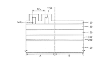
図2Aを参照すれば、基板100上の高密度パターン領域A及び低密度パターン領域Bに、それぞれパッド酸化膜210及び窒化膜212を順次形成する。
次いで、図1A及び図1Bを参照して説明したような方法で、窒化膜212上に第1ハードマスク層120、第2ハードマスク層130、モールド層140及び反射防止膜142を順次形成し、高密度パターン領域Aで反射防止膜142上にフォトレジストパターン144を形成する。
2A to 2G, the same reference numerals as those in FIGS. 1A to 1K represent the same members, and detailed descriptions thereof will be omitted.
Referring to FIG. 2A, a
Next, the first
図2Bを参照すれば、図1Cを参照して説明したような方法で、基板100上の高密度パターン領域Aで、第2ハードマスク層130上に複数のモールドパターン140aを形成する。
次いで、図1Dを参照して説明したような方法で、高密度パターン領域Aでモールドパターン140aの上面及び側壁と第2ハードマスク層130の上面とを均一な厚さで覆うと同時に、低密度パターン領域Bで第2ハードマスク層130の上面を均一な厚さで覆う微細マスク層150を形成する。
Referring to FIG. 2B, a plurality of
Next, in the method described with reference to FIG. 1D, the upper surface and sidewalls of the
図2Cを参照すれば、図1Eから図1Gを参照して説明したような方法で、高密度パターン領域Aでモールドパターン140aの両側壁に形成される複数の微細スペーサ150aと、低密度パターン領域Bに形成される低密度マスクパターン150bとを同時に形成する。低密度マスクパターン150bは、微細スペーサ150aの第1幅W1より大きい第2幅W2を持つように形成される。
Referring to FIG. 2C, a plurality of
図2Dを参照すれば、図1Hを参照して説明したような方法で、モールドパターン140a及び上部ハードマスクパターン160aを除去した後、図1Iおよび図1Jを参照して説明したような方法で、複数の微細スペーサ150a及び低密度マスクパターン150bをエッチングマスクとして、高密度パターン領域A及び低密度パターン領域Bで同時に第2ハードマスク層130を異方性ドライエッチングして、高密度の第2ハードマスクパターン130a及び低密度の第2ハードマスクパターン130bを形成した後、これをエッチングマスクとして第1ハードマスク層120を異方性ドライエッチングして、高密度パターン領域A及び低密度パターン領域Bで、それぞれ窒化膜212上に高密度第1ハードマスクパターン120a及び低密度第1ハードマスクパターン120bを形成する。
Referring to FIG. 2D, after the
図2Eを参照すれば、図1Kを参照して説明した通りに、高密度パターン領域A及び低密度パターン領域Bで、それぞれ高密度第1ハードマスクパターン120a及び低密度第1ハードマスクパターン120bをエッチングマスクとして、窒化膜212を異方性ドライエッチングする。その結果、高密度パターン領域A及び低密度パターン領域Bには、それぞれ高密度窒化膜パターン212a及び低密度窒化膜パターン212bが形成される。
Referring to FIG. 2E, as described with reference to FIG. 1K, the high-density first
図2Eには、高密度窒化膜パターン212a及び低密度窒化膜パターン212b上に、高密度第1ハードマスクパターン120a及び低密度第1ハードマスクパターン120bが残っていないと図示されている。しかし、場合によって高密度窒化膜パターン212a及び低密度窒化膜パターン212bが形成された後、高密度窒化膜パターン212a及び低密度窒化膜パターン212bの上面に、それぞれ高密度第1ハードマスクパターン120a及び低密度第1ハードマスクパターン120bが残留していることもある。
FIG. 2E illustrates that the high-density first
図2Fを参照すれば、高密度窒化膜パターン212a及び低密度窒化膜パターン212bをエッチングマスクとして、パッド酸化膜210及び基板100を異方性ドライエッチングする。その結果、高密度パターン領域A及び低密度パターン領域Bには、それぞれ高密度活性領域260a及び低密度活性領域260bを限定する高密度トレンチ262a及び低密度トレンチ262bが形成される。
Referring to FIG. 2F, the
図2Gを参照すれば、高密度トレンチ262a及び低密度トレンチ262bの内部と、高密度窒化膜パターン212a及び低密度窒化膜パターン212b上に絶縁物質を蒸着した後、これを高密度窒化膜パターン212a及び低密度窒化膜パターン212bが露出されるまでCMP(Chemical Mechanical Polishing)工程により平坦化して、高密度トレンチ262a及び低密度トレンチ262b内にそれぞれ素子分離膜270を形成する。
Referring to FIG. 2G, after an insulating material is deposited on the
図2Aから図2Gを参照して説明した方法のように、本実施形態による方法により基板上の相異なる領域で相異なるパターン密度を持つ微細マスクパターンを同時に形成した後、これをエッチングマスクとして利用して前記基板をエッチングしてトレンチを形成することによって、基板上で形成しようとする単位素子の種類及び密度によって、基板に多様な幅及び多様なピッチを持つ活性領域を比較的単純な工程により定義できる。 Like the method described with reference to FIGS. 2A to 2G, after the micro mask patterns having different pattern densities are simultaneously formed in different regions on the substrate by the method according to the present embodiment, this is used as an etching mask. Then, by etching the substrate to form a trench, active regions having various widths and various pitches can be formed on the substrate by a relatively simple process according to the type and density of unit elements to be formed on the substrate. Can be defined.
以上、本発明を望ましい実施形態を挙げて詳細に説明したが、本発明は前記実施形態に限定されず、本発明の技術的思想及び範囲内で当業者によっていろいろな変形及び変更が可能である。 The present invention has been described in detail with reference to preferred embodiments. However, the present invention is not limited to the above-described embodiments, and various modifications and changes can be made by those skilled in the art within the technical idea and scope of the present invention. .
本発明は、半導体素子関連の技術分野に好適に用いられる。 The present invention is suitably used in the technical field related to semiconductor devices.
100:基板、110:被エッチング膜、110a:低密度パターン、110b:高密度パターン、120:第1ハードマスク層、120a:高密度第1ハードマスクパターン、120b:低密度第1ハードマスクパターン、130:第2ハードマスク層、130a:高密度第2ハードマスクパターン、130b:低密度第2ハードマスクパターン、140:モールド層、140a:モールドパターン、142:反射防止膜、144:フォトレジストパターン、150:微細マスク層、150a:微細スペーサ、150b:低密度マスクパターン、160:上部ハードマスク層、160a:上部ハードマスクパターン、162:反射防止膜、164:フォトレジストパターン、210:パッド酸化膜、212:窒化膜、212a:高密度窒化膜パターン、212b:低密度窒化膜パターン、260a:高密度活性領域、260b:低密度活性領域、262a:高密度トレンチ、262b:低密度トレンチ、270:素子分離膜、A:高密度パターン領域、B:低密度パターン領域 100: substrate, 110: film to be etched, 110a: low density pattern, 110b: high density pattern, 120: first hard mask layer, 120a: high density first hard mask pattern, 120b: low density first hard mask pattern, 130: second hard mask layer, 130a: high density second hard mask pattern, 130b: low density second hard mask pattern, 140: mold layer, 140a: mold pattern, 142: antireflection film, 144: photoresist pattern, 150: fine mask layer, 150a: fine spacer, 150b: low density mask pattern, 160: upper hard mask layer, 160a: upper hard mask pattern, 162: antireflection film, 164: photoresist pattern, 210: pad oxide film, 212: nitride film, 212a: high density nitriding Pattern, 212b: low density nitride film pattern, 260a: high density active region, 260b: low density active region, 262a: high density trench, 262b: low density trench, 270: element isolation film, A: high density pattern region, B : Low density pattern area
Claims (20)
前記第1領域で前記モールドパターンを覆う微細マスク層を、前記基板上の第1領域及び前記第2領域に同時に形成するステップと、
前記第1領域及び前記第2領域のうち、前記第2領域のみに前記微細マスク層の上面のうち一部を覆う上部ハードマスクパターンを形成するステップと、
前記上部ハードマスクパターンをエッチングマスクとして、前記第1領域及び前記第2領域で前記微細マスク層をエッチングし、前記第1領域には、前記微細マスク層の第1部分で形成される複数の微細スペーサを前記複数のモールドパターンそれぞれの両側壁に形成すると同時に、前記第2領域には前記微細マスク層の第2部分で形成される低密度マスクパターンを形成するステップと、を含むことを特徴とする半導体素子の微細パターン形成方法。 Forming a plurality of mold patterns repeatedly arranged at a first pitch only on the first region of the first region and the second region on a substrate including the first region and the second region;
Forming a fine mask layer covering the mold pattern in the first region simultaneously in the first region and the second region on the substrate;
Forming an upper hard mask pattern that covers a part of the upper surface of the fine mask layer only in the second region of the first region and the second region;
Using the upper hard mask pattern as an etching mask, the fine mask layer is etched in the first region and the second region, and a plurality of fine portions formed by the first portion of the fine mask layer are formed in the first region. Forming a spacer on both side walls of each of the plurality of mold patterns, and simultaneously forming a low-density mask pattern formed in the second portion of the fine mask layer in the second region. A method for forming a fine pattern of a semiconductor device.
前記第2領域で前記低密度マスクパターンは、前記第1パターン密度よりさらに低い第2パターン密度で形成されることを特徴とする請求項1に記載の半導体素子の微細パターン形成方法。 In the first region, the plurality of fine spacers are formed with a first pattern density,
2. The method of claim 1, wherein the low-density mask pattern is formed at a second pattern density lower than the first pattern density in the second region.
前記複数の微細スペーサ及び低密度マスクパターンが形成された後、前記複数の微細スペーサ及び低密度マスクパターンをエッチングマスクとして、前記第1領域及び前記第2領域で前記被エッチング膜をエッチングするステップをさらに含むことを特徴とする請求項1に記載の半導体素子の微細パターン形成方法。 The substrate includes an etching target film, and the plurality of mold patterns and the fine mask layer are respectively formed on the etching target film.
Etching the film to be etched in the first region and the second region using the plurality of fine spacers and the low density mask pattern as an etching mask after the plurality of fine spacers and the low density mask pattern are formed; The method for forming a fine pattern of a semiconductor device according to claim 1, further comprising:
前記複数のモールドパターン及び前記微細マスク層は、それぞれ前記下部ハードマスク層上に形成されることを特徴とする請求項1に記載の半導体素子の微細パターン形成方法。 The substrate includes a semiconductor substrate and a lower hard mask layer formed on the semiconductor substrate,
The method of claim 1, wherein the plurality of mold patterns and the fine mask layer are respectively formed on the lower hard mask layer.
前記第1領域及び前記第2領域で前記微細マスク層上に上部ハードマスク層を形成するステップと、
前記第1領域及び前記第2領域のうち、前記第2領域のみに前記上部ハードマスク層の上面のうち一部を覆うマスクパターンを形成するステップと、
前記マスクパターンをエッチングマスクとして、前記上部ハードマスク層をエッチングして前記上部ハードマスクパターンを形成するステップと、を含むことを特徴とする請求項1に記載の半導体素子の微細パターン形成方法。 Forming the upper hard mask pattern comprises:
Forming an upper hard mask layer on the fine mask layer in the first region and the second region;
Forming a mask pattern covering a part of the upper surface of the upper hard mask layer only in the second region of the first region and the second region;
The method of claim 1, further comprising: etching the upper hard mask layer to form the upper hard mask pattern using the mask pattern as an etching mask.
前記第1除去工程及び第2除去工程は、それぞれドライエッチング工程、ウェットエッチング工程、及びアッシング工程中で選択されるいずれか一つの工程により行なわれ、
前記第1除去工程及び第2除去工程は、相異なる工程で行なわれることを特徴とする請求項17に記載の半導体素子の微細パターン形成方法。 The step of removing the plurality of mold patterns and the upper hard mask pattern includes a first removal process for removing the plurality of mold patterns and a second removal process for removing the upper hard mask pattern. ,
The first removal step and the second removal step are each performed by any one selected from a dry etching step, a wet etching step, and an ashing step,
The method of claim 17, wherein the first removal step and the second removal step are performed in different steps.
Applications Claiming Priority (4)
| Application Number | Priority Date | Filing Date | Title |
|---|---|---|---|
| KR1020080029329A KR101448854B1 (en) | 2008-03-28 | 2008-03-28 | Method of forming fine patterns of semiconductor device |
| KR10-2008-0029329 | 2008-03-28 | ||
| US12/217,782 | 2008-07-09 | ||
| US12/217,782 US7998357B2 (en) | 2008-03-28 | 2008-07-09 | Method of fine patterning semiconductor device |
Publications (2)
| Publication Number | Publication Date |
|---|---|
| JP2009246332A true JP2009246332A (en) | 2009-10-22 |
| JP5323438B2 JP5323438B2 (en) | 2013-10-23 |
Family
ID=41117894
Family Applications (1)
| Application Number | Title | Priority Date | Filing Date |
|---|---|---|---|
| JP2008261675A Expired - Fee Related JP5323438B2 (en) | 2008-03-28 | 2008-10-08 | Method for forming fine pattern of semiconductor element |
Country Status (4)
| Country | Link |
|---|---|
| US (1) | US7998357B2 (en) |
| JP (1) | JP5323438B2 (en) |
| KR (1) | KR101448854B1 (en) |
| CN (1) | CN101546693B (en) |
Cited By (1)
| Publication number | Priority date | Publication date | Assignee | Title |
|---|---|---|---|---|
| JP2015005662A (en) * | 2013-06-21 | 2015-01-08 | 株式会社東芝 | Pattern formation method |
Families Citing this family (14)
| Publication number | Priority date | Publication date | Assignee | Title |
|---|---|---|---|---|
| KR101653149B1 (en) * | 2010-07-06 | 2016-09-02 | 에스케이하이닉스 주식회사 | Method for fabricating contact hole in semiconductor device |
| KR101169164B1 (en) * | 2010-10-27 | 2012-07-30 | 에스케이하이닉스 주식회사 | Semiconductor device and method for forming the same |
| KR20130015145A (en) * | 2011-08-02 | 2013-02-13 | 삼성전자주식회사 | Method of forming fine patterns for semiconductor device |
| US8557675B2 (en) | 2011-11-28 | 2013-10-15 | Globalfoundries Inc. | Methods of patterning features in a structure using multiple sidewall image transfer technique |
| US8669186B2 (en) | 2012-01-26 | 2014-03-11 | Globalfoundries Inc. | Methods of forming SRAM devices using sidewall image transfer techniques |
| KR102564551B1 (en) | 2016-01-26 | 2023-08-04 | 삼성전자주식회사 | Method for manufacturing the semiconductor device |
| CN108231770B (en) * | 2016-12-22 | 2021-05-04 | 联华电子股份有限公司 | Method for forming pattern |
| US11127594B2 (en) * | 2017-12-19 | 2021-09-21 | Tokyo Electron Limited | Manufacturing methods for mandrel pull from spacers for multi-color patterning |
| US10475648B1 (en) | 2018-05-01 | 2019-11-12 | United Microelectronics Corp. | Method for patterning a semiconductor structure |
| US10658427B2 (en) * | 2018-10-18 | 2020-05-19 | Micron Technology, Inc. | Memory for embedded applications |
| CN111383920A (en) * | 2018-12-29 | 2020-07-07 | 中芯国际集成电路制造(上海)有限公司 | Semiconductor structure and forming method thereof |
| CN110783272B (en) * | 2019-10-17 | 2022-05-27 | 上海华力集成电路制造有限公司 | Truncation process method of fin field effect transistor |
| CN111430231A (en) * | 2020-05-21 | 2020-07-17 | 中国科学院微电子研究所 | Planarization method and semiconductor device |
| US11444180B2 (en) * | 2020-08-09 | 2022-09-13 | Nanya Technology Corporation | Method of forming uniform fin features |
Citations (4)
| Publication number | Priority date | Publication date | Assignee | Title |
|---|---|---|---|---|
| JP2001188357A (en) * | 1999-12-28 | 2001-07-10 | Matsushita Electric Ind Co Ltd | Method and device for forming resin film to substrate for display element as well as method for manufacturing liquid crystal display device using the method |
| JP2004361637A (en) * | 2003-06-04 | 2004-12-24 | Tokyo Ohka Kogyo Co Ltd | Positive photoresist composition for manufacture of liquid crystal display (lcd) and method for forming resist pattern |
| WO2006101695A1 (en) * | 2005-03-15 | 2006-09-28 | Micron Technology, Inc. | Pitch reduced patterns relative to photolithography features |
| WO2007117718A2 (en) * | 2006-04-07 | 2007-10-18 | Micron Technology, Inc. | Simplified pitch doubling process flow |
Family Cites Families (4)
| Publication number | Priority date | Publication date | Assignee | Title |
|---|---|---|---|---|
| KR100354440B1 (en) | 2000-12-04 | 2002-09-28 | 삼성전자 주식회사 | Method for forming patterns of semiconductor device |
| US7115525B2 (en) * | 2004-09-02 | 2006-10-03 | Micron Technology, Inc. | Method for integrated circuit fabrication using pitch multiplication |
| KR100640640B1 (en) * | 2005-04-19 | 2006-10-31 | 삼성전자주식회사 | Method of forming fine pattern of semiconductor device using fine pitch hardmask |
| KR100672123B1 (en) * | 2006-02-02 | 2007-01-19 | 주식회사 하이닉스반도체 | Method for forming micro pattern in semiconductor device |
-
2008
- 2008-03-28 KR KR1020080029329A patent/KR101448854B1/en not_active IP Right Cessation
- 2008-07-09 US US12/217,782 patent/US7998357B2/en not_active Expired - Fee Related
- 2008-09-27 CN CN2008101492915A patent/CN101546693B/en active Active
- 2008-10-08 JP JP2008261675A patent/JP5323438B2/en not_active Expired - Fee Related
Patent Citations (4)
| Publication number | Priority date | Publication date | Assignee | Title |
|---|---|---|---|---|
| JP2001188357A (en) * | 1999-12-28 | 2001-07-10 | Matsushita Electric Ind Co Ltd | Method and device for forming resin film to substrate for display element as well as method for manufacturing liquid crystal display device using the method |
| JP2004361637A (en) * | 2003-06-04 | 2004-12-24 | Tokyo Ohka Kogyo Co Ltd | Positive photoresist composition for manufacture of liquid crystal display (lcd) and method for forming resist pattern |
| WO2006101695A1 (en) * | 2005-03-15 | 2006-09-28 | Micron Technology, Inc. | Pitch reduced patterns relative to photolithography features |
| WO2007117718A2 (en) * | 2006-04-07 | 2007-10-18 | Micron Technology, Inc. | Simplified pitch doubling process flow |
Cited By (1)
| Publication number | Priority date | Publication date | Assignee | Title |
|---|---|---|---|---|
| JP2015005662A (en) * | 2013-06-21 | 2015-01-08 | 株式会社東芝 | Pattern formation method |
Also Published As
| Publication number | Publication date |
|---|---|
| KR20090103612A (en) | 2009-10-01 |
| CN101546693B (en) | 2012-11-14 |
| US7998357B2 (en) | 2011-08-16 |
| CN101546693A (en) | 2009-09-30 |
| KR101448854B1 (en) | 2014-10-14 |
| JP5323438B2 (en) | 2013-10-23 |
| US20090246966A1 (en) | 2009-10-01 |
Similar Documents
| Publication | Publication Date | Title |
|---|---|---|
| JP5323438B2 (en) | Method for forming fine pattern of semiconductor element | |
| US7842601B2 (en) | Method of forming small pitch pattern using double spacers | |
| US7709396B2 (en) | Integral patterning of large features along with array using spacer mask patterning process flow | |
| US7473647B2 (en) | Method of forming pattern using fine pitch hard mask | |
| KR100843236B1 (en) | Method of forming fine patterns of semiconductor device using double patterning process | |
| US7563712B2 (en) | Method of forming micro pattern in semiconductor device | |
| US8623771B2 (en) | Method for fabricating micropattern of semiconductor device | |
| US7919414B2 (en) | Method for forming fine patterns in semiconductor device | |
| JP5356762B2 (en) | Method for forming fine pattern of semiconductor element | |
| US20090068838A1 (en) | Method for forming micropatterns in semiconductor device | |
| US8110340B2 (en) | Method of forming a pattern of a semiconductor device | |
| US20090068842A1 (en) | Method for forming micropatterns in semiconductor device | |
| US8304175B2 (en) | Patterning method | |
| KR20090076743A (en) | Method of forming fine patterns of semiconductor device | |
| KR20100098843A (en) | Methods of forming a pattern | |
| KR100832016B1 (en) | Method for fabricating landing plug conatct in semiconductor device | |
| KR100792386B1 (en) | Method for fabricating semiconductor device | |
| CN107045974B (en) | Method for manufacturing semiconductor device | |
| KR20070113604A (en) | Method for forming micro pattern of semiconductor device | |
| JP2009010156A (en) | Pattern forming method | |
| KR20080061165A (en) | Method of manufacturing a contact hole in semiconductor device | |
| KR20100039572A (en) | Method of manufacturing flash memory device |
Legal Events
| Date | Code | Title | Description |
|---|---|---|---|
| A621 | Written request for application examination |
Free format text: JAPANESE INTERMEDIATE CODE: A621 Effective date: 20110928 |
|
| A977 | Report on retrieval |
Free format text: JAPANESE INTERMEDIATE CODE: A971007 Effective date: 20121005 |
|
| A131 | Notification of reasons for refusal |
Free format text: JAPANESE INTERMEDIATE CODE: A131 Effective date: 20121012 |
|
| A521 | Request for written amendment filed |
Free format text: JAPANESE INTERMEDIATE CODE: A523 Effective date: 20121228 |
|
| TRDD | Decision of grant or rejection written | ||
| A01 | Written decision to grant a patent or to grant a registration (utility model) |
Free format text: JAPANESE INTERMEDIATE CODE: A01 Effective date: 20130621 |
|
| A61 | First payment of annual fees (during grant procedure) |
Free format text: JAPANESE INTERMEDIATE CODE: A61 Effective date: 20130717 |
|
| R150 | Certificate of patent or registration of utility model |
Free format text: JAPANESE INTERMEDIATE CODE: R150 |
|
| R250 | Receipt of annual fees |
Free format text: JAPANESE INTERMEDIATE CODE: R250 |
|
| R250 | Receipt of annual fees |
Free format text: JAPANESE INTERMEDIATE CODE: R250 |
|
| LAPS | Cancellation because of no payment of annual fees |