JP2009212173A - Wafer film cutting apparatus - Google Patents
Wafer film cutting apparatus Download PDFInfo
- Publication number
- JP2009212173A JP2009212173A JP2008051556A JP2008051556A JP2009212173A JP 2009212173 A JP2009212173 A JP 2009212173A JP 2008051556 A JP2008051556 A JP 2008051556A JP 2008051556 A JP2008051556 A JP 2008051556A JP 2009212173 A JP2009212173 A JP 2009212173A
- Authority
- JP
- Japan
- Prior art keywords
- film
- wafer
- base
- unit
- cutting
- Prior art date
- Legal status (The legal status is an assumption and is not a legal conclusion. Google has not performed a legal analysis and makes no representation as to the accuracy of the status listed.)
- Ceased
Links
- 238000005520 cutting process Methods 0.000 title claims abstract description 66
- 238000011084 recovery Methods 0.000 claims abstract description 10
- 230000002093 peripheral effect Effects 0.000 claims description 7
- 238000002844 melting Methods 0.000 abstract description 5
- 230000008018 melting Effects 0.000 abstract description 5
- 238000010438 heat treatment Methods 0.000 abstract description 3
- 230000007547 defect Effects 0.000 abstract 1
- 239000010408 film Substances 0.000 description 163
- 235000012431 wafers Nutrition 0.000 description 112
- 239000000853 adhesive Substances 0.000 description 16
- 230000001070 adhesive effect Effects 0.000 description 16
- 238000004519 manufacturing process Methods 0.000 description 9
- 239000010409 thin film Substances 0.000 description 7
- 238000000034 method Methods 0.000 description 6
- 230000000694 effects Effects 0.000 description 5
- 238000004140 cleaning Methods 0.000 description 2
- 229910003460 diamond Inorganic materials 0.000 description 2
- 239000010432 diamond Substances 0.000 description 2
- 238000009713 electroplating Methods 0.000 description 2
- 238000001179 sorption measurement Methods 0.000 description 2
- 230000032258 transport Effects 0.000 description 2
- 238000011109 contamination Methods 0.000 description 1
- 230000000994 depressogenic effect Effects 0.000 description 1
- 238000010586 diagram Methods 0.000 description 1
- 238000005516 engineering process Methods 0.000 description 1
- 238000001459 lithography Methods 0.000 description 1
- 239000000155 melt Substances 0.000 description 1
- 230000001681 protective effect Effects 0.000 description 1
- 239000004065 semiconductor Substances 0.000 description 1
Images




Landscapes
- Perforating, Stamping-Out Or Severing By Means Other Than Cutting (AREA)
- Container, Conveyance, Adherence, Positioning, Of Wafer (AREA)
Abstract
Description
本発明は、ウエハフィルム裁断装置に関する。特にウエハ上方に位置するフィルムプレス上、下台によってフィルム裁断を行い、ウエハ面積より大きい或いは同等のフィルム体を裁断することができる効果を達成するウエハフィルム裁断装置に係る。 The present invention relates to a wafer film cutting apparatus. In particular, the present invention relates to a wafer film cutting apparatus that achieves an effect of cutting a film body that is larger than or equivalent to the wafer area by performing film cutting with a lower base on a film press located above the wafer.
公知のウエハフィルム裁断装置は、長方形のフィルムをウエハ上に接着し、さらにレーザー或いはダイヤモンドカッターにより余分な部分を除去する。レーザー或いはダイヤモンドカッターとウエハとの接触を避けるため、その裁断されたフィルムはウエハ面積より大きくなければならない。しかし、ウエハ製造工程に対応するため、ウエハ外周を巡ってフィルム非接着領域を残す必要があるため、現行技術では露光或いはリソグラフ方式によって余分なフィルムを除去している。
しかし、この種の方式では製造工程のステップ及びコストを増大させてしまう。よって一般的には先ずフィルムを予め裁断し、次に手作業で所定の寸法形状となったフィルムをウエハ上に置いているが、この種の方式は効率が極めて悪いため、生産能力を向上させることができない。
A known wafer film cutting apparatus bonds a rectangular film onto a wafer, and further removes an excess portion with a laser or a diamond cutter. In order to avoid contact between the laser or diamond cutter and the wafer, the cut film must be larger than the wafer area. However, in order to cope with the wafer manufacturing process, it is necessary to leave a film non-adhesive region around the outer periphery of the wafer. Therefore, in the current technology, excess film is removed by exposure or lithographic method.
However, this type of system increases the steps and costs of the manufacturing process. Therefore, in general, the film is first cut in advance, and then a film having a predetermined size and shape is manually placed on the wafer. However, this type of method is extremely inefficient and improves the production capacity. I can't.
これらの事情を踏まえ、改善方式が提案された。中華民国特許申請案第096202954号「ウエハのフィルム接着裁断機」は水平な台体上に枠フレーム体、上接着裁断機構、下接着裁断機構、供給ユニット、排出料ユニットを設置する。
該枠フレーム体は該台体上に設置し、該上接着裁断機構は該枠フレーム体下方においてオーバーハング設置する。
該上接着裁断機構は、該枠フレーム体に対応し数本の可動棒によって上下移動を行う。該上接着裁断機構底部には上外環体、内環体、刃片環を設置する。
該下接着裁断機構は、該上接着裁断機構下方の台体位置に設置し、底板、下外環体、セットテーブルを含む。
該供給ユニットは該下接着裁断機構片側に設置し、ロール状フィルムを設置し、供給する。
該排出ユニットは該下接着裁断機構の該進料ユニットに相対する反対側に設置し、ロール状フィルムを巻き取ることができる。
公知のフィルム裁断設備では該上接着裁断機構の下降移動によって、該上外環体が先ず下圧してフィルムを展張し、該内環体をウエハを置くセットテーブル上まで下降させ、これによりフィルムをウエハと枠フレーム頂面に接着し、同時に該内環体外周の刃片環が下降してフィルムを切断する。さらに吸気ユニットによってフィルムをウエハ上に密着させる。
しかし、この種の公知設備はフィルムをウエハ上に接着する前に、先ずフィルムを拡張させて張る必要があり、その後にウエハに接着するため、ステップが多く、しかもフィルムをウエハに接着する時、衝突が起こり易い。これによりウエハは損傷するため、使用において理想的ではない。さらに、フィルムはウエハ上に接着し、その後にフィルムの裁断を行うため、刃片環とウエハの衝突を避けるため、このフィルムはウエハより大きくなければならない。このためウエハ外周縁に線路を設置する必要があり、これによりフィルムはウエハよりやや小さい或いは同等とする。よって該公知設備はニーズに応えることはできない。
Based on these circumstances, an improvement method was proposed. The Chinese Patent Application No. 096202954 "Wafer Film Bonding Cutting Machine" has a frame body, an upper bonding cutting mechanism, a lower bonding cutting mechanism, a supply unit, and a discharge unit on a horizontal base.
The frame frame body is installed on the base body, and the upper adhesive cutting mechanism is installed overhanging below the frame frame body.
The upper adhesive cutting mechanism moves up and down by several movable bars corresponding to the frame body. An upper outer ring body, an inner ring body, and a blade piece ring are installed at the bottom of the upper adhesive cutting mechanism.
The lower adhesive cutting mechanism is installed at a base position below the upper adhesive cutting mechanism, and includes a bottom plate, a lower outer ring, and a set table.
The supply unit is installed on one side of the lower adhesive cutting mechanism, and a roll film is installed and supplied.
The discharge unit is installed on the opposite side of the lower adhesive cutting mechanism to the fee unit, and can roll up a roll film.
In the known film cutting equipment, the upper outer ring body first pressurizes and stretches the film by the downward movement of the upper adhesive cutting mechanism, and the inner ring body is lowered onto the set table on which the wafer is placed. The wafer and the frame frame are bonded to the top surface, and at the same time, the blade ring on the outer periphery of the inner ring is lowered to cut the film. Further, the film is brought into close contact with the wafer by the intake unit.
However, this kind of known equipment requires that the film is first stretched and stretched before bonding the film onto the wafer, and then has many steps to bond to the wafer, and when the film is bonded to the wafer, Collisions are likely to occur. This damages the wafer and is not ideal for use. In addition, the film must be larger than the wafer in order to adhere to the wafer and subsequently cut the film, so as to avoid collision between the blade ring and the wafer. For this reason, it is necessary to install a track on the outer periphery of the wafer, so that the film is slightly smaller or equivalent to the wafer. Therefore, this known facility cannot meet the needs.
また、特開昭63−096907号公報の「半導体保護膜の自動フィルム裁断装置」では、ロール装置を利用し薄膜を輸送し、裁断しようとする薄膜をウエハ表面上まで輸送し、下ピストンによってウエハを受け止め、該下ピストンを上から下へと作動させ、これにより該ウエハ外周縁の円形カッターは突出し、上ピストンが下方へとプッシュして薄膜を裁断し、裁断された薄膜をウエハと共に横へと移動させる。
この種の公知方式はウエハ外周縁の円形カッターを設置し、中央に位置したウエハをウエハ積載する下ピストンによってウエハを薄膜と共に下方へと移動させ、上ピストンを下方へと作動させて薄膜を裁断するものである。しかし、カッターはウエハ外周縁に位置するため、裁断を経た薄膜は当然ウエハより大きく、同様に、フィルムをウエハより小さくするとのニーズに応えることはできない。しかもこの種の公知設備の円形カッターはウエハをウエハ積載する下ピストン外周縁に設置するため、円形カッターサイズの変更は非常に面倒で、製造工程での利用には不便である。
さらに、上記2種の公知方式は共に一回に一単位のウエハのフィルム裁断、接着しか行うことができないため、全体的な生産能力には限界がある。同一製造工程において大量の機械を調達しなければならないとすれば、莫大な資金を必要とし、コストを押し上げる結果となってしまう。
In this type of known method, a circular cutter is installed at the outer periphery of the wafer, the wafer is moved downward together with the thin film by the lower piston for loading the wafer located at the center, and the thin film is cut by operating the upper piston downward. To do. However, since the cutter is located at the outer peripheral edge of the wafer, the thin film that has been cut is naturally larger than the wafer, and similarly, the need to make the film smaller than the wafer cannot be met. In addition, since the circular cutter of this kind of known equipment is installed on the outer peripheral edge of the lower piston on which the wafer is loaded, changing the size of the circular cutter is very troublesome and inconvenient for use in the manufacturing process.
Furthermore, since the above two known methods can only perform film cutting and bonding of one unit of wafer at a time, there is a limit to the overall production capacity. If a large number of machines must be procured in the same manufacturing process, a huge amount of money is required, resulting in an increase in cost.
本発明が解決しようとする課題は、公知のフィルム裁断装置のウエハより小さい或いは同等のフィルム体を裁断することができず、しかも一回に一単位のフィルム体しか裁断することができず、また裁断サイズを簡単に変更することができないという欠接点を改善することができるウエハフィルム裁断装置を提供することである。 The problem to be solved by the present invention is that a film body smaller than or equivalent to a wafer of a known film cutting apparatus cannot be cut, and only one unit of film body can be cut at a time. It is an object of the present invention to provide a wafer film cutting apparatus that can improve a missing contact that the cutting size cannot be easily changed.
上記課題を解決するため、本発明は下記のウエハフィルム裁断装置を提供する。
フィルムプレス上台、フィルムプレス下台、フィルム供給ユニット、フィルム回収ユニット、ウエハ積載ユニットを設置し、
該フィルムプレス上台は複数の上刃台を設置し、
該フィルムプレス下台上方端面には複数の下刃台を設置し、該下刃台内直径はウエハの直径より小さい或いは同等で、該フィルムプレス下台下方端面にはウエハ収容部を陥没設置し該下刃台と連通し、該ウエハ収容部外周縁には肩部を環状に設置し、しかも該肩部高度はウエハ厚度より大きく、
該フィルムプレス上台上方には吸着盤台を設置し、該吸着盤台下方端面には複数の吸着盤を設置し、該吸着盤はちょうど該フィルムプレス上台の上刃台に対応し設置し、該吸着盤内側にはそれぞれ少なくとも一個の接着ユニットを設置し、該接着ユニットは熱溶融効果を提供するための装置で、これにより裁断が完了したフィルム体は熱溶融を受けウエハ上に接着し、
公知のフィルム裁断装置は、露光或いはリソグラフステップを行い、或いは手作業によりフィルム体を置く必要があるが、これでは一回に一単位のフィルム体しか切除できず、しかもカッター裁断方式の制限を受け、ウエハ面積より大きいフィルム体しか裁断することができず、ウエハ面積より小さい或いは同等に裁断することができず、カッター裁断のサイズを変更することもできない。
本発明は、ウエハウエハ積載ユニット上方に位置するフィルムプレス上、下台を利用し複数の上、下刃台を設置し、一回のプレス裁断作業を行うだけで複数のフィルム体を裁断することができ、生産能力を向上させることができ、露光或いはリソグラフ等ステップを省くことができる。
本発明は、ウエハ上に設置する上、下刃台によってフィルム体を裁断し、該下刃台内直径はウエハ直径より小さい或いは同等で、ウエハ面積より小さい或いは同等のフィルム体を裁断することができ、使用者はウエハ外周縁において電気メッキ接点設定に用いることができ、しかも該フィルム体は吸着盤により先に吸引上昇して次に下ろし、これにより裁断の残りかすを掃除することができ、ウエハの汚染を回避可能である。
また、該吸着盤内側には接着ユニットを設置して、フィルム体を加熱溶融し、フィルム体がウエハ上に置かれると、ちょうどウエハ上に接着し、フィルム接着の効果を達成する。
さらに、該フィルムプレス上台及び該フィルムプレス下台は交換可能で、異なるサイズの上、下刃台に交換し、各種ウエハサイズに対応可能で、こうして他の機械を調達する必要なく、異なるサイズのウエハのフィルム裁断作業を行うことができる。
In order to solve the above problems, the present invention provides the following wafer film cutting apparatus.
Installed a film press upper base, film press lower base, film supply unit, film recovery unit, wafer stacking unit,
The film press upper base is provided with a plurality of upper blade bases,
A plurality of lower blade bases are installed on the upper end surface of the film press lower base, and the inner diameter of the lower blade base is smaller than or equal to the diameter of the wafer. It communicates with the blade base, and a shoulder portion is annularly installed on the outer peripheral edge of the wafer accommodating portion, and the shoulder height is larger than the wafer thickness,
An upper surface of the film press is provided with a suction platen base, and a plurality of suction plates are provided on the lower end surface of the suction platen base. At least one adhesive unit is installed inside each suction disk, and the adhesive unit is a device for providing a thermal melting effect, whereby the film body that has been cut is subjected to thermal melting and bonded onto the wafer,
Known film cutting devices require exposure, lithographic steps or manual placement of the film body, but this can only cut one unit of film body at a time and is limited by the cutter cutting method. Only the film body larger than the wafer area can be cut, and the film can be cut smaller than or equal to the wafer area, and the cutter cutting size cannot be changed.
The present invention can cut a plurality of film bodies only by performing a single press cutting operation by installing a plurality of upper and lower blade bases using a lower base on a film press positioned above the wafer wafer stacking unit. Production capacity can be improved, and steps such as exposure or lithography can be omitted.
In the present invention, the film body is cut on the wafer by the lower blade base on the wafer, and the inner diameter of the lower blade base is smaller than or equal to the wafer diameter, and the film body smaller than or equal to the wafer area can be cut. Can be used for setting the electroplating contact point at the outer periphery of the wafer, and the film body is first sucked up and then lowered by the suction disk, thereby cleaning the residue of cutting, Wafer contamination can be avoided.
In addition, an adhesive unit is installed inside the suction plate, the film body is heated and melted, and when the film body is placed on the wafer, it is just bonded onto the wafer to achieve the effect of film adhesion.
In addition, the film press upper base and the film press lower base can be exchanged, and can be exchanged for different wafer sizes by changing to different size upper and lower blade bases. Thus, there is no need to procure other machines, and thus different size wafers can be obtained. The film cutting operation can be performed.
上記のように、本発明はウエハ面積より小さい、或いは同等のフィルム体に裁断することが可能となり、複数のフィルム体を裁断することもでき、裁断サイズを変更することも容易である。 As described above, the present invention can be cut into a film body that is smaller than or equivalent to the wafer area, a plurality of film bodies can be cut, and the cutting size can be easily changed.
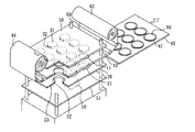
本発明ウエハフィルム裁断装置は、図1及び図2に示すように、フィルムプレス上台10、フィルムプレス下台20、フィルム供給ユニット61、フィルム回収ユニット62、ウエハ積載ユニット40、プッシュユニット50を設置する。
該フィルムプレス上台10は、該フィルムプレス下台20の上方に位置して固定され、該フィルムプレス上台10は、複数の上刃台11を設置する。該上刃台11は、該フィルムプレス上台10下面に配置され、内部に陥没した円形状開口構造を呈し、かつ該上刃台11内側壁の下方端面内径は上方端面内径より大きい。
該フィルムプレス下台20は、上下昇降可能な構造で、該フィルムプレス下台20は複数の下刃台21を設置し、該下刃台21は該フィルムプレス下台20上面に配置され、凸出した円形開口状構造を呈し、該下刃台21上下内径は相同で、真っ直ぐで平坦な内側壁を呈する。該下刃台21外側壁の上方外径は下方外径より小さく、しかも該下刃台21内直径はウエハ41の直径より小さい或いは同等である。これにより、該下刃台21はちょうど該上刃台11内に収容され、凸出した下刃台21の凸出した外周縁は該上刃台11内側壁の傾斜角度に対応する。
該フィルムプレス下台20下面には、上記下刃台21と対応する位置にウエハ収容部22を陥没して設けてフィルムプレス下台の円形開口を連通して開口する。該ウエハ収容部22外周縁には肩部23を環状に形成し、該肩部23の厚さウエハ41厚さより大きい。
As shown in FIGS. 1 and 2, the wafer film cutting apparatus of the present invention is provided with a film press
The film press
The film press
On the lower surface of the film press
該フィルム供給ユニット61及び該フィルム回収ユニット62はそれぞれ該フィルムプレス上台10、該フィルムプレス下台20の進行方向前後に配置される。該フィルム供給ユニット61及び該フィルム回収ユニット62にはロール式のフィルム体60を設置する。該フィルム体60は、該フィルムプレス上台10及び該フィルムプレス下台20の間を通って配置され、該フィルムプレス上台10の下面に接する。該フィルム供給ユニット61は、未裁断フィルム体60を送り出し、該フィルム回収ユニット62は裁断後のフィルム体60を巻き取って回収する。
該フィルムプレス上台10上方には吸着盤台30を設置し、該吸着盤台30下方端面には複数の吸着盤31を設置する。該吸着盤31は、ちょうど該フィルムプレス上台10の上刃台11の位置に対応して配置する。該吸着盤31は、真空吸引力により該上刃台11、該下刃台21の裁断を経たフィルム体60を吸引して上に上げる。
該吸着盤31内側にはそれぞれ少なくとも一個の接着ユニット32を設置する。該接着ユニット32は、熱溶融効果を提供するための装置で、裁断が完了したフィルム体60は熱溶融を受けて該ウエハ41上に接着する。
The
An adsorbing
At least one
作業時には、該ウエハ積載ユニット40は該フィルムプレス下台20下方に移動し、該フィルム供給ユニット61は該ウエハ積載ユニット40の移動に対応して裁断されていないフィルム体60を送り出す。該吸着盤台30は該上刃台11、該下刃台21に対応して配置された吸着盤31によって、先ず未裁断のフィルム体60を上方へと吸引し、該フィルムプレス上台10の下面に密着させる。
該プッシュユニット50は、油圧或いは気圧等の技術手段により、下から上へとプッシュ板台51を該ウエハ積載ユニット40と共に押上げて上昇させ、これにより該ウエハ積載ユニット40はフィルムプレス下台20に押し当てられる。該フィルムプレス下台20と該ウエハ積載ユニット40の接触面にはウエハ収容部22が介在し、該ウエハ収容部22の凹部内径は該ウエハ積載ユニット40上のウエハ41より大きく、外周側には肩部23が形成されているため、該肩部23が該ウエハ積載ユニット40に接触して支持することにより、該ウエハ41は該フィルムプレス下台20と接触しない。
該プッシュユニット50がさらに上昇すると、該フィルムプレス下台20と該フィルムプレス上台10は接合し、該下刃台21は該上刃台11内に収容される。こうして該フィルムプレス下台20と該フィルムプレス上台10の間に位置するフィルム体60は該上刃台11、該下刃台21により円形に裁断される。
また該吸着盤31は、裁断作業前に既にフィルム体60を吸着しているため、裁断後は該フィルム体60を吸引上昇し、該吸着盤31内側に設置された接着ユニット32は該フィルム体60を加熱溶融する。このとき、該吸着盤31は残余のフィルム体60と分離して裁断フィルム体60をウエハ41上に接着することができる。これによりフィルム裁断と接着の効果を達成し、ウエハ41表面積より小さいフィルム体60を裁断することができる。
In operation, the
The
When the
Further, since the
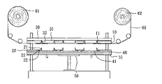
図3〜図6の操作指示図中の図3に示すように、該ウエハ積載ユニット40上に複数のウエハ41を載置し、該ウエハ積載ユニット40は機械アーム、コンベアベルト(図示なし)等の移送手段によって該フィルムプレス下台20下方に移動し、該フィルムプレス上台10、該フィルムプレス上台10両側に位置するフィルム供給ユニット61及び該フィルム回収ユニット62は使用済みのフィルム体60を巻き取り、未裁断のフィルム体60を該フィルムプレス下台20及び該フィルムプレス上台10の間に送る。
As shown in FIG. 3 in the operation instruction diagrams of FIGS. 3 to 6, a plurality of
図4に示すように、該吸着盤台30はスタート時には未裁断のフィルム体60を上方へと吸引し、該フィルムプレス上台10下面に密着させる。該プッシュユニット50は該ウエハ積載ユニット40を下から上へと押し上げ、該ウエハ積載ユニット40は上方へと該フィルムプレス下台20を押し上げる。該フィルムプレス下台20と該ウエハ積載ユニット40の接触面にはウエハ収容部22が位置するため、該ウエハ収容部22は外側肩部23によって該ウエハ積載ユニット40に当接し、これにより該ウエハ41は該フィルムプレス下台20と一切接触することがなくなり、ウエハ41の損傷を回避することができる。
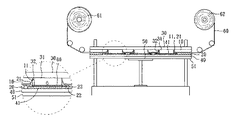
図5に示すように、該ウエハ積載ユニット40は、該フィルムプレス下台20と共に該プッシュユニット50に続けて押し上げられ、該フィルムプレス下台20と該フィルムプレス下台20は接合し、該下刃台21は該上刃台11に嵌入し、該フィルムプレス上台10と該フィルムプレス下台20間に位置するフィルム体60は該上刃台11と該下刃台21の嵌合により円形に裁断される。該下刃台21は該上刃台11内に嵌設され、該下刃台21内直径はウエハ41直径より小さい或いは同等であるため、裁断されたフィルム体60はウエハ41表面積より小さいか或いは同等である。裁断工程のスタート時には未裁断のフィルム体60は該吸着盤台30により吸着されているため、該上刃台11及び該下刃台21が接合してフィルム体60を裁断すると、該裁断後のフィルム体60は吸引上昇し、フィルム体60裁断により残留する残余のフィルム体の掃除に便利である。こうしてウエハ41は汚染を回避可能で、該吸着盤31内側には接着ユニット32を設置するため、該接着ユニット32は吸引上昇したフィルム体60周縁を加熱溶融する。
As shown in FIG. 4, at the start, the
As shown in FIG. 5, the
図6及び図7に示すように、該吸着盤31の吸引作業が終了すると、該吸着盤台30は熱溶融済みのフィルム体60を下方へ下降させてウエハ41上に接着し、フィルム接着する。前記の下刃台21内直径はウエハ41直径より小さいか或いは同等であるため、裁断されたフィルム体60の面積はウエハ41面積より小さいか或いは同等である。こうしてウエハ41外周に電気メッキ接点を形成することができる。
さらに該フィルムプレス上台10、該フィルムプレス下台20は複数の上刃台11、下刃台21を設置するため、同時に複数のフィルム体60をプレス裁断可能で、生産能力を高めることができる。
フィルム裁断後、該プッシュユニット50は下降し、それに伴って該プッシュ板台51、該ウエハ積載ユニット40が下降する。該フィルムプレス下台20は押されなくなり元の位置に戻り、機械アーム、コンベアベルト等の移送手段により該ウエハ積載ユニット40をウエハ41、ウエハ41に接着されたフィルム体60と共に自動圧フィルム機に送り圧合し、或いは真空圧フィルム機に送り圧合し、及び他の製造工程ステップへと送る。
As shown in FIGS. 6 and 7, when the suction operation of the
Furthermore, since the film press
After the film cutting, the
10 フィルムプレス上台
11 上刃台
20 フィルムプレス下台
21 下刃台
22 ウエハ収容部
23 肩部
30 吸着盤台
31 吸着盤
32 接着ユニット
40 ウエハ積載ユニット
41 ウエハ
50 プッシュユニット
51 プッシュ板台
60 フィルム体
61 フィルム供給ユニット
62 フィルム回収ユニット
DESCRIPTION OF
Claims (6)
該フィルムプレス上台及びフィルムプレス下台は、それぞれ相対して上下に配置されると共にそれぞれ相対する一以上の上及び下刃台を設け、
該フィルムプレス下台は、その上面に向けて環状の裁断刃を具えた下刃台を設けると共にその裁断刃よりも大きいウエハ収容部を下刃台裁断形状の開口に連通してその下面に凹部として形成し、
該フィルムプレス上台の上刃台にはこれと対応する環状の裁断刃を具え、
これら上記上下刃台の裁断寸法をウエハと同等以下とし、
該フィルムプレス下台下方には該フィルムプレス下台を昇降させるプッシュユニットを設置し、
該プッシュユニットにより該フィルムプレス下台を上昇させて上記上刃台と下刃台の間でフィルムを裁断し、裁断されたフィルムを上記エハ収容部内のウエハに供給する
ことを特徴とするウエハフィルム裁断装置。 It consists of a film press upper base, a film press lower base, and a push unit.
The film press upper base and the film press lower base are respectively arranged one above the other and provided with one or more upper and lower blade bases facing each other,
The film press lower base is provided with a lower blade base having an annular cutting blade toward the upper surface thereof, and a wafer accommodating portion larger than the cutting blade is communicated with the opening of the lower blade base cutting shape so as to form a recess on the lower surface. Forming,
The upper cutter rest of the upper film press has an annular cutting blade corresponding thereto,
The cutting dimensions of these upper and lower blade bases are equal to or less than the wafer,
A push unit for raising and lowering the film press lower base is installed below the film press lower base,
Wafer film cutting characterized in that the film press lower base is raised by the push unit to cut the film between the upper blade base and the lower blade base, and the cut film is supplied to the wafer in the wafer housing portion. apparatus.
Priority Applications (1)
| Application Number | Priority Date | Filing Date | Title |
|---|---|---|---|
| JP2008051556A JP2009212173A (en) | 2008-03-03 | 2008-03-03 | Wafer film cutting apparatus |
Applications Claiming Priority (1)
| Application Number | Priority Date | Filing Date | Title |
|---|---|---|---|
| JP2008051556A JP2009212173A (en) | 2008-03-03 | 2008-03-03 | Wafer film cutting apparatus |
Publications (1)
| Publication Number | Publication Date |
|---|---|
| JP2009212173A true JP2009212173A (en) | 2009-09-17 |
Family
ID=41185062
Family Applications (1)
| Application Number | Title | Priority Date | Filing Date |
|---|---|---|---|
| JP2008051556A Ceased JP2009212173A (en) | 2008-03-03 | 2008-03-03 | Wafer film cutting apparatus |
Country Status (1)
| Country | Link |
|---|---|
| JP (1) | JP2009212173A (en) |
Cited By (6)
| Publication number | Priority date | Publication date | Assignee | Title |
|---|---|---|---|---|
| CN104716021A (en) * | 2013-12-13 | 2015-06-17 | 朗姆研究公司 | Methods and systems for forming semiconductor laminate structures |
| CN106783680A (en) * | 2016-12-12 | 2017-05-31 | 北京中电科电子装备有限公司 | A kind of semiconductor manufacturing equipment membrane treatment appts and method |
| CN109079912A (en) * | 2018-09-06 | 2018-12-25 | 苏州滕艺科技有限公司 | Apertured film attaches die-cutting device |
| JP6454812B1 (en) * | 2018-08-09 | 2019-01-16 | 信越エンジニアリング株式会社 | Work transfer chuck and work transfer method |
| CN113290628A (en) * | 2021-05-26 | 2021-08-24 | 苏州安洁科技股份有限公司 | Processing technology for conductive cloth and conductive foam |
| CN116825653A (en) * | 2023-05-25 | 2023-09-29 | 广东派顿新能源有限公司 | Photovoltaic panel assembly preparation method based on recovered silicon wafer and photovoltaic panel assembly |
Citations (3)
| Publication number | Priority date | Publication date | Assignee | Title |
|---|---|---|---|---|
| JPS6396907A (en) * | 1986-10-13 | 1988-04-27 | Ryoji Wakabayashi | Automatic punching machine for protective film at semiconductor wafer |
| JP2000065996A (en) * | 1998-08-19 | 2000-03-03 | Konica Corp | Method for cutting lamination body and method for cutting stimulable phosphor plate |
| JP2002367931A (en) * | 2001-06-07 | 2002-12-20 | Lintec Corp | Die bonding sheet sticking apparatus and die bonding sheet sticking method |
-
2008
- 2008-03-03 JP JP2008051556A patent/JP2009212173A/en not_active Ceased
Patent Citations (3)
| Publication number | Priority date | Publication date | Assignee | Title |
|---|---|---|---|---|
| JPS6396907A (en) * | 1986-10-13 | 1988-04-27 | Ryoji Wakabayashi | Automatic punching machine for protective film at semiconductor wafer |
| JP2000065996A (en) * | 1998-08-19 | 2000-03-03 | Konica Corp | Method for cutting lamination body and method for cutting stimulable phosphor plate |
| JP2002367931A (en) * | 2001-06-07 | 2002-12-20 | Lintec Corp | Die bonding sheet sticking apparatus and die bonding sheet sticking method |
Cited By (8)
| Publication number | Priority date | Publication date | Assignee | Title |
|---|---|---|---|---|
| CN104716021A (en) * | 2013-12-13 | 2015-06-17 | 朗姆研究公司 | Methods and systems for forming semiconductor laminate structures |
| CN104716021B (en) * | 2013-12-13 | 2019-04-09 | 朗姆研究公司 | Method and system for forming semiconductor stack structures |
| CN106783680A (en) * | 2016-12-12 | 2017-05-31 | 北京中电科电子装备有限公司 | A kind of semiconductor manufacturing equipment membrane treatment appts and method |
| JP6454812B1 (en) * | 2018-08-09 | 2019-01-16 | 信越エンジニアリング株式会社 | Work transfer chuck and work transfer method |
| CN109079912A (en) * | 2018-09-06 | 2018-12-25 | 苏州滕艺科技有限公司 | Apertured film attaches die-cutting device |
| CN109079912B (en) * | 2018-09-06 | 2024-06-07 | 苏州滕艺科技有限公司 | Die cutting equipment for attaching porous film |
| CN113290628A (en) * | 2021-05-26 | 2021-08-24 | 苏州安洁科技股份有限公司 | Processing technology for conductive cloth and conductive foam |
| CN116825653A (en) * | 2023-05-25 | 2023-09-29 | 广东派顿新能源有限公司 | Photovoltaic panel assembly preparation method based on recovered silicon wafer and photovoltaic panel assembly |
Similar Documents
| Publication | Publication Date | Title |
|---|---|---|
| JP5273791B2 (en) | Equipment for applying adhesive tape to substrates | |
| JP5543812B2 (en) | Adhesive tape application method and adhesive tape application device | |
| KR101352484B1 (en) | Vaccum lamination system and vaccum lamination molding method | |
| JP6636696B2 (en) | Semiconductor wafer mounting method and semiconductor wafer mounting apparatus | |
| JP2011199158A (en) | Workpiece transfer method and workpiece transfer device | |
| KR101819162B1 (en) | A vacuum laminator for bonding adhesive film to carrier wafer and a method for operating the same | |
| KR102327469B1 (en) | Adhesive tape attaching method and adhesive tape attaching apparatus | |
| TW200845286A (en) | Method for joining adhesive tape and apparatus using the method | |
| JP2009044008A5 (en) | ||
| JP2004349435A (en) | Device for attaching dicing die-bond tape to substrate | |
| JP4941944B2 (en) | Method and apparatus for attaching adhesive tape to substrate | |
| JP2015162634A (en) | Device of pasting protective tape to wafer and method of manufacturing wafer | |
| JP2012216606A (en) | Substrate transfer method and substrate transfer device | |
| JP2009246067A5 (en) | ||
| CN202498808U (en) | Battery Automatic Laminating Machine | |
| JP6298381B2 (en) | Substrate laminating method and substrate laminating apparatus | |
| CN218255505U (en) | A wafer cutting device | |
| TWI353646B (en) | ||
| KR100921390B1 (en) | Wafer Membrane Cutting Machine | |
| JP2011091118A (en) | Wafer laminate dicing saw | |
| JP2019040941A (en) | Adhesive tape affixing device to substrate and affixing method | |
| CN210477830U (en) | A keyboard hot melt film integrated equipment | |
| JP6653032B2 (en) | Semiconductor wafer mounting method and semiconductor wafer mounting apparatus | |
| JP2005230883A (en) | Automatic press apparatus | |
| CN218602406U (en) | Wafer carrying platform for circular cutting |
Legal Events
| Date | Code | Title | Description |
|---|---|---|---|
| A131 | Notification of reasons for refusal |
Free format text: JAPANESE INTERMEDIATE CODE: A131 Effective date: 20100812 |
|
| A977 | Report on retrieval |
Free format text: JAPANESE INTERMEDIATE CODE: A971007 Effective date: 20100812 |
|
| A521 | Written amendment |
Free format text: JAPANESE INTERMEDIATE CODE: A523 Effective date: 20101104 |
|
| A521 | Written amendment |
Free format text: JAPANESE INTERMEDIATE CODE: A523 Effective date: 20101207 |
|
| RD02 | Notification of acceptance of power of attorney |
Free format text: JAPANESE INTERMEDIATE CODE: A7422 Effective date: 20101207 |
|
| A01 | Written decision to grant a patent or to grant a registration (utility model) |
Free format text: JAPANESE INTERMEDIATE CODE: A01 Effective date: 20110111 |
|
| A601 | Written request for extension of time |
Free format text: JAPANESE INTERMEDIATE CODE: A601 Effective date: 20110112 |
|
| A602 | Written permission of extension of time |
Free format text: JAPANESE INTERMEDIATE CODE: A602 Effective date: 20110117 |
|
| A045 | Written measure of dismissal of application |
Free format text: JAPANESE INTERMEDIATE CODE: A045 Effective date: 20110624 |