JP2009188223A - Semiconductor device - Google Patents
Semiconductor device Download PDFInfo
- Publication number
- JP2009188223A JP2009188223A JP2008027246A JP2008027246A JP2009188223A JP 2009188223 A JP2009188223 A JP 2009188223A JP 2008027246 A JP2008027246 A JP 2008027246A JP 2008027246 A JP2008027246 A JP 2008027246A JP 2009188223 A JP2009188223 A JP 2009188223A
- Authority
- JP
- Japan
- Prior art keywords
- region
- channel
- channel region
- conductivity type
- semiconductor device
- Prior art date
- Legal status (The legal status is an assumption and is not a legal conclusion. Google has not performed a legal analysis and makes no representation as to the accuracy of the status listed.)
- Withdrawn
Links
- 239000004065 semiconductor Substances 0.000 title claims abstract description 49
- 239000000758 substrate Substances 0.000 claims 5
- 239000011347 resin Substances 0.000 abstract description 2
- 229920005989 resin Polymers 0.000 abstract description 2
- 238000007789 sealing Methods 0.000 abstract description 2
- 230000035882 stress Effects 0.000 description 21
- 238000000034 method Methods 0.000 description 10
- 238000010586 diagram Methods 0.000 description 7
- 230000000694 effects Effects 0.000 description 4
- 238000004519 manufacturing process Methods 0.000 description 3
- WHXSMMKQMYFTQS-UHFFFAOYSA-N Lithium Chemical compound [Li] WHXSMMKQMYFTQS-UHFFFAOYSA-N 0.000 description 2
- 229910052744 lithium Inorganic materials 0.000 description 2
- 238000004806 packaging method and process Methods 0.000 description 2
- 238000012858 packaging process Methods 0.000 description 2
- 229910021420 polycrystalline silicon Inorganic materials 0.000 description 2
- 229920005591 polysilicon Polymers 0.000 description 2
- 230000006641 stabilisation Effects 0.000 description 2
- 238000011105 stabilization Methods 0.000 description 2
- XUIMIQQOPSSXEZ-UHFFFAOYSA-N Silicon Chemical compound [Si] XUIMIQQOPSSXEZ-UHFFFAOYSA-N 0.000 description 1
- 230000015572 biosynthetic process Effects 0.000 description 1
- 238000001514 detection method Methods 0.000 description 1
- 229910052710 silicon Inorganic materials 0.000 description 1
- 239000010703 silicon Substances 0.000 description 1
- 230000008646 thermal stress Effects 0.000 description 1
Images


Classifications
-
- H—ELECTRICITY
- H01—ELECTRIC ELEMENTS
- H01L—SEMICONDUCTOR DEVICES NOT COVERED BY CLASS H10
- H01L21/00—Processes or apparatus adapted for the manufacture or treatment of semiconductor or solid state devices or of parts thereof
- H01L21/70—Manufacture or treatment of devices consisting of a plurality of solid state components formed in or on a common substrate or of parts thereof; Manufacture of integrated circuit devices or of parts thereof
- H01L21/77—Manufacture or treatment of devices consisting of a plurality of solid state components or integrated circuits formed in, or on, a common substrate
- H01L21/78—Manufacture or treatment of devices consisting of a plurality of solid state components or integrated circuits formed in, or on, a common substrate with subsequent division of the substrate into plural individual devices
- H01L21/82—Manufacture or treatment of devices consisting of a plurality of solid state components or integrated circuits formed in, or on, a common substrate with subsequent division of the substrate into plural individual devices to produce devices, e.g. integrated circuits, each consisting of a plurality of components
- H01L21/822—Manufacture or treatment of devices consisting of a plurality of solid state components or integrated circuits formed in, or on, a common substrate with subsequent division of the substrate into plural individual devices to produce devices, e.g. integrated circuits, each consisting of a plurality of components the substrate being a semiconductor, using silicon technology
- H01L21/8232—Field-effect technology
- H01L21/8234—MIS technology, i.e. integration processes of field effect transistors of the conductor-insulator-semiconductor type
- H01L21/823412—MIS technology, i.e. integration processes of field effect transistors of the conductor-insulator-semiconductor type with a particular manufacturing method of the channel structures, e.g. channel implants, halo or pocket implants, or channel materials
-
- H—ELECTRICITY
- H01—ELECTRIC ELEMENTS
- H01L—SEMICONDUCTOR DEVICES NOT COVERED BY CLASS H10
- H01L21/00—Processes or apparatus adapted for the manufacture or treatment of semiconductor or solid state devices or of parts thereof
- H01L21/02—Manufacture or treatment of semiconductor devices or of parts thereof
- H01L21/04—Manufacture or treatment of semiconductor devices or of parts thereof the devices having at least one potential-jump barrier or surface barrier, e.g. PN junction, depletion layer or carrier concentration layer
- H01L21/18—Manufacture or treatment of semiconductor devices or of parts thereof the devices having at least one potential-jump barrier or surface barrier, e.g. PN junction, depletion layer or carrier concentration layer the devices having semiconductor bodies comprising elements of Group IV of the Periodic System or AIIIBV compounds with or without impurities, e.g. doping materials
-
- H—ELECTRICITY
- H01—ELECTRIC ELEMENTS
- H01L—SEMICONDUCTOR DEVICES NOT COVERED BY CLASS H10
- H01L23/00—Details of semiconductor or other solid state devices
- H01L23/12—Mountings, e.g. non-detachable insulating substrates
-
- H—ELECTRICITY
- H01—ELECTRIC ELEMENTS
- H01L—SEMICONDUCTOR DEVICES NOT COVERED BY CLASS H10
- H01L27/00—Devices consisting of a plurality of semiconductor or other solid-state components formed in or on a common substrate
- H01L27/02—Devices consisting of a plurality of semiconductor or other solid-state components formed in or on a common substrate including semiconductor components specially adapted for rectifying, oscillating, amplifying or switching and having at least one potential-jump barrier or surface barrier; including integrated passive circuit elements with at least one potential-jump barrier or surface barrier
- H01L27/04—Devices consisting of a plurality of semiconductor or other solid-state components formed in or on a common substrate including semiconductor components specially adapted for rectifying, oscillating, amplifying or switching and having at least one potential-jump barrier or surface barrier; including integrated passive circuit elements with at least one potential-jump barrier or surface barrier the substrate being a semiconductor body
- H01L27/08—Devices consisting of a plurality of semiconductor or other solid-state components formed in or on a common substrate including semiconductor components specially adapted for rectifying, oscillating, amplifying or switching and having at least one potential-jump barrier or surface barrier; including integrated passive circuit elements with at least one potential-jump barrier or surface barrier the substrate being a semiconductor body including only semiconductor components of a single kind
- H01L27/085—Devices consisting of a plurality of semiconductor or other solid-state components formed in or on a common substrate including semiconductor components specially adapted for rectifying, oscillating, amplifying or switching and having at least one potential-jump barrier or surface barrier; including integrated passive circuit elements with at least one potential-jump barrier or surface barrier the substrate being a semiconductor body including only semiconductor components of a single kind including field-effect components only
- H01L27/088—Devices consisting of a plurality of semiconductor or other solid-state components formed in or on a common substrate including semiconductor components specially adapted for rectifying, oscillating, amplifying or switching and having at least one potential-jump barrier or surface barrier; including integrated passive circuit elements with at least one potential-jump barrier or surface barrier the substrate being a semiconductor body including only semiconductor components of a single kind including field-effect components only the components being field-effect transistors with insulated gate
-
- H—ELECTRICITY
- H01—ELECTRIC ELEMENTS
- H01L—SEMICONDUCTOR DEVICES NOT COVERED BY CLASS H10
- H01L29/00—Semiconductor devices adapted for rectifying, amplifying, oscillating or switching, or capacitors or resistors with at least one potential-jump barrier or surface barrier, e.g. PN junction depletion layer or carrier concentration layer; Details of semiconductor bodies or of electrodes thereof ; Multistep manufacturing processes therefor
- H01L29/66—Types of semiconductor device ; Multistep manufacturing processes therefor
- H01L29/68—Types of semiconductor device ; Multistep manufacturing processes therefor controllable by only the electric current supplied, or only the electric potential applied, to an electrode which does not carry the current to be rectified, amplified or switched
- H01L29/76—Unipolar devices, e.g. field effect transistors
- H01L29/772—Field effect transistors
- H01L29/78—Field effect transistors with field effect produced by an insulated gate
Abstract
Description
本発明は、高精度な半導体装置およびその製造方法に関する。 The present invention relates to a highly accurate semiconductor device and a manufacturing method thereof.
電圧検出器(VD)、電圧レギュレータ(VR)、リチウム電池保護IC等の電源ICにおいては、近年、更なる高精度化が要求されている。通常、高精度を実現する為には、ウエハー製造工程(前工程)段階で発生した製造ばらつきを、ウエハーテスト工程(後工程)において、ポリシリコン製のヒューズをレーザー等によってトリミングして特性値を合わせこみ、高精度を実現するなどの手法が取られている。 In recent years, there has been a demand for higher precision in power supply ICs such as a voltage detector (VD), a voltage regulator (VR), and a lithium battery protection IC. Normally, in order to achieve high accuracy, manufacturing variations that occurred in the wafer manufacturing process (pre-process) are trimmed in the wafer test process (post-process) using a polysilicon fuse or the like to obtain characteristic values. Techniques such as fitting and achieving high accuracy are taken.
しかし、このようにして高精度に作成したチップでも、パッケージング工程やプリント基板への実装工程に於ける特性変化があると、場合によっては製品仕様を満たせない事態が発生する。パッケージング工程や基板実装工程での特性変化の原因は、熱応力による素子特性の変化と考えられる。すなわち、これらの工程を経ることによって半導体チップに応力がかかり、若しくは加えられた熱によって応力のかかり方が変化することで、ポリシリコン抵抗の抵抗値やトランジスタの閾値電圧などが変化するのである。 However, even if the chip is manufactured with high accuracy in this way, if there is a change in characteristics in the packaging process or the mounting process on the printed circuit board, the situation where the product specifications cannot be satisfied may occur. The cause of the characteristic change in the packaging process or the board mounting process is considered to be a change in element characteristics due to thermal stress. That is, through these steps, stress is applied to the semiconductor chip, or the manner in which the stress is applied by the applied heat changes, thereby changing the resistance value of the polysilicon resistor, the threshold voltage of the transistor, and the like.
こうした変化を防止する為に、プリント基板への実装後に半導体製品の特性を調整できるようにしておくなどの発明が開示されている(例えば、特許文献1参照)。しかしながら、引用した発明の工程は複雑であり、実現するのはコスト的に難しいと考えられ、よりシンプルでコスト的に見合った特性値安定化手法が望まれている。
本願発明が解決しようとする問題点は、以下のとおりである。 The problems to be solved by the present invention are as follows.
半導体製品をパッケージングするにあたって、高精度の半導体製品の特性が変化してしまう。この原因は、前述したとおり応力による素子特性の変化と考えられる。例えば封止樹脂から半導体チップに対して応力がかかり、ピエゾ抵抗効果によって素子の抵抗値、特性が変化する。近年、部品の小型化要求により、小型のパッケージへの実装が盛んに行われているが、それに伴って半導体チップの薄型化も進んでいる。半導体チップが薄型化すればするほど、同じ応力がかかった場合、より大きく半導体チップがひずみ、より大きな特性変化が発生する懸念がある。特性の変化量は、例えばリチウム電池保護ICの過充電検出電圧にして数mVといった程度の変化であるが、高精度の製品においてこの変化量は無視できないものである。 When packaging semiconductor products, the characteristics of highly accurate semiconductor products change. The cause of this is considered to be a change in element characteristics due to stress as described above. For example, stress is applied to the semiconductor chip from the sealing resin, and the resistance value and characteristics of the element change due to the piezoresistance effect. In recent years, due to demands for miniaturization of components, mounting on small packages has been actively performed, and accordingly, semiconductor chips have been made thinner. As the semiconductor chip becomes thinner, there is a concern that when the same stress is applied, the semiconductor chip is more distorted and a larger characteristic change occurs. The amount of change in characteristics is, for example, a change of about several millivolts when the overcharge detection voltage of a lithium battery protection IC is used. However, this amount of change cannot be ignored in high-precision products.
一方、高精度な半導体製品においては、対を形成したトランジスタ間で特性が同じであることを利用して高精度を実現している。例えば、カレントミラー回路は、対を形成するPチャネルMOSトランジスタ間で同一な電流が流れることを利用して、2つの電流経路の電流が等しくなるように働くことを利用した回路である。通常、対を成すトランジスタはその特性が大きく違わないように、半導体製品内で出来るだけ近く、可能であれば隣接しておくことが望ましい。また、そのチャネル方向も揃えて置くことが特性安定化に寄与する。 On the other hand, in high-precision semiconductor products, high accuracy is realized by utilizing the fact that the characteristics of the paired transistors are the same. For example, a current mirror circuit is a circuit that uses the fact that the same current flows between P-channel MOS transistors that form a pair and works to make the currents of two current paths equal. In general, it is desirable that the paired transistors be as close as possible in the semiconductor product, and adjacent if possible, so that the characteristics are not greatly different. In addition, the channel direction is also aligned to contribute to characteristic stabilization.
このような半導体製品に応力がかかり、特性値の変動(シフト)が発生する。このとき、対を形成しているトランジスタ間で不均一な応力がかかった場合、すなわちそれぞれのトランジスタにかかる応力が違った場合に、それぞれのトランジスタでの特性値変動が違う事になる。本発明は、このような応力による特性値変動を低減することが可能な半導体装置を提供することを目的とする。 Stress is applied to such a semiconductor product, and the characteristic value fluctuates (shifts). At this time, when non-uniform stress is applied between the transistors forming the pair, that is, when the stress applied to each transistor is different, the characteristic value variation in each transistor is different. An object of the present invention is to provide a semiconductor device capable of reducing such fluctuations in characteristic values due to stress.
上記課題を解決するために、本発明は次の手段を用いた。 In order to solve the above problems, the present invention uses the following means.
応力とキャリアの進行方向のなす角度依存性を利用し、素子特性の応力による変化を相殺し、結果として特性変化を低減する事を特徴とする半導体装置とした。 The semiconductor device is characterized in that the change in the element characteristic due to the stress is canceled by utilizing the angle dependency between the stress and the traveling direction of the carrier, and as a result, the characteristic change is reduced.
また、別の手段として、対を形成するトランジスタ間で応力のかかりかたを均等にすることで特性変化を低減する事を特徴とする半導体装置とした。 As another means, the semiconductor device is characterized in that the characteristic change is reduced by equalizing the stress applied between the transistors forming the pair.
この発明を用いることにより、半導体装置の実装時の特性値変動を従来よりも低減することが可能となり、より高精度の半導体装置を実現することが可能となる。 By using this invention, it becomes possible to reduce the characteristic value fluctuation at the time of mounting of a semiconductor device as compared with the prior art, and it becomes possible to realize a more accurate semiconductor device.
以下、本発明の実施の形態を図1〜図4に基づいて説明する。 Hereinafter, embodiments of the present invention will be described with reference to FIGS.
半導体素子は、実装時の応力によるピエゾ抵抗効果によってキャリアの移動度が変化し、素子の抵抗値、若しくは電流値が変化することが知られている。MOSトランジスタにおいては、特に移動度の変化による相互コンダクタンスGm値の変化が顕著に見られる。そうすると、カレントミラーなど対となったトランジスタ間のGm値が一定であることを前提とした回路ではこの実装による応力での特性値変化が無視できないほど大きくなる。ここで例に示したカレントミラー回路を考えると、対を形成しているトランジスタ間でGm値の変化量ΔGmが異なる場合に回路としての特性値変動を生じることとなる。 It is known that a semiconductor element has a carrier mobility that changes due to a piezoresistive effect due to stress during mounting, and the resistance value or current value of the element changes. In the MOS transistor, the change in the mutual conductance Gm value due to the change in mobility is particularly noticeable. Then, in a circuit based on the premise that the Gm value between the paired transistors such as a current mirror is constant, the characteristic value change due to the stress due to this mounting becomes so large that it cannot be ignored. Considering the current mirror circuit shown as an example here, when the change amount ΔGm of the Gm value differs between the transistors forming a pair, the characteristic value fluctuation as a circuit occurs.
そこで、こういった特性値に影響の大きい対を形成したトランジスタ間の特性値変動、ここではGm値の変動を等しくすることで、対を成すトランジスタ間の特性値変動を相殺する事が可能となる。実装時にチップにかかる応力を測定、若しくはシミュレーションする事で予測し、素子にかかる応力の大きさと、応力とチャネルがなす角度が対となったトランジスタ間で同一になるようにレイアウトを行なう。このことにより、対となったトランジスタ間でのシフトが同じになるため、結果的にパッケージング時の特性変化を低減することが可能となる。 Therefore, it is possible to cancel the characteristic value fluctuation between the paired transistors by equalizing the characteristic value fluctuation between the transistors forming a pair having a large influence on the characteristic value, in this case, the Gm value fluctuation. Become. The stress applied to the chip at the time of mounting is predicted by measuring or simulating, and the layout is performed so that the magnitude of the stress applied to the element and the angle between the stress and the channel are the same between the paired transistors. As a result, the shift between the paired transistors becomes the same, and as a result, it is possible to reduce characteristic changes during packaging.
シリコン半導体のピエゾ抵抗効果は面方位依存性を示すが、この面方位依存性を利用して、シフトを低減するという手法をとる。例えば、<110>方向の正孔移動度は応力の方向に対する角度が垂直の場合と平行の場合で、逆の変動を示すことが判っている。この効果を利用し、チャネルの形成される方向を一方向に限定せず、直交した角度をもつようにレイアウトを工夫してひとつのトランジスタを形成することにより、それぞれの応力に対するシフト方向が反対であるため、シフト同士が相殺され、結果として特性値変動を低減することが可能となる。 The piezoresistive effect of a silicon semiconductor shows a plane orientation dependence, and a technique of reducing the shift by utilizing this plane orientation dependence is taken. For example, it has been found that the hole mobility in the <110> direction shows opposite fluctuations when the angle with respect to the direction of the stress is vertical and parallel. By taking advantage of this effect, the direction of channel formation is not limited to one direction, but the layout is devised so as to have an orthogonal angle so that one transistor is formed. Therefore, the shifts are canceled out, and as a result, the characteristic value fluctuation can be reduced.
図1には、本発明の第1の実施例の模式図を示した。第一のソース電極4と第一のゲート電極6と第一のドレイン電極8と第一のゲート電極直下にゲート絶縁膜とチャネル領域を有する第一のトランジスタ10と、第二のソース電極5と第二のゲート電極7と第二のドレイン電極9と第二のゲート電極直下にゲート絶縁膜とチャネル領域を有する第二のトランジスタ11とが互いのソース電極で接続され、かつ、互いのトランジスタのチャネル角度が90°異なって配置されている。一方のトランジスタ10では半導体チップの1辺に対し垂直方向のチャネルが形成され、他方のトランジスタ11では該1辺に対し平行方向のチャネルが形成される。このようにチャネル方向が垂直方向のトランジスタと平行方向のトランジスタを組み合わせることで、各々のトランジスタ動作時の特性値変動を相殺することが可能となる。
FIG. 1 shows a schematic diagram of the first embodiment of the present invention. A
実際の回路においては、このようにして、異なるチャネル角度を有する複数のトランジスタをさらに対を形成して配置することになる。これによって、特性値の変動が小さな高精度な回路を形成できる。 In an actual circuit, a plurality of transistors having different channel angles are arranged in pairs in this way. This makes it possible to form a highly accurate circuit with small variation in characteristic values.
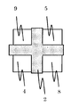
図2には、本発明における第2の実施例の模式図を示した。チャネル領域を覆うようにゲート絶縁膜とゲート電極2が十字型に形成されており、チャネル領域によって区切られた4つの領域のうち2つの領域には、ソース領域およびソース電極4、5が対向するように配置され、残りの2つの領域には、ドレイン領域およびドレイン電極8、9が対向するように配置されている。チャネル領域が十字型であるため、その直交した成分同士がトランジスタ動作時の特性値変動を相殺することが可能となる。
In FIG. 2, the schematic diagram of the 2nd Example in this invention was shown. The gate insulating film and the
図3には、本発明における第3の実施例の模式図を示した。矩形帯状のチャネル領域の内側にはドレイン領域3、チャネル領域の外側にはソース領域1が配置され、かつチャネル領域を覆うようにゲート絶縁膜とゲート電極が形成されている。トランジスタが動作した場合、4方向のチャネルが形成され、これらが互いの特性変動を相殺するように働く。図3では矩形帯状のチャネル領域を例に説明したが、このチャネル領域は環状であっても良い。すなわち、環状のチャネル領域の内側にはドレイン領域、チャネル領域の外側にはソース領域が配置され、かつチャネル領域を覆うようにゲート絶縁膜とゲート電極が形成されている。トランジスタが動作するとチャネルは全方向に形成されるため、特性値変動のより効率的な相殺が可能となる。
In FIG. 3, the schematic diagram of the 3rd Example in this invention was shown. A
また、別の実施例として、図4に示すように、トランジスタを配置するという方法もある(コモンセントロイド配置)。第一のソース電極4と第一のゲート電極6と第一のドレイン電極8と第一のゲート電極直下にゲート絶縁膜とチャネル領域を有しタスキがけ状に配置された第一のトランジスタ10および13のゲート電極およびドレイン電極をそれぞれ接続し、第二のソース電極5と第二のゲート電極7と第二のドレイン電極9と第二のゲート電極直下にゲート絶縁膜とチャネル領域を有しタスキがけ状に配置された第二のトランジスタ11および12のゲート電極およびドレイン電極をそれぞれ接続し、各々のトランジスタのソース電極は、トランジスタ11、10、12,13の順にシリーズに接続するものである。
As another embodiment, there is a method of arranging transistors as shown in FIG. 4 (common centroid arrangement). A
この配置は、前述の実施例で見られた様なチャネルと応力のなす角度が2つ以上有り、それらが直交しているわけではない。しかし、タスキがけ状に配置することで、結果的にシフトを低減することが可能となる。この配置により、半導体チップ内の応力分布があった場合に、ペアトランジスタ間でかかる応力の平均値が均一になるという効果が生じる。この効果によって、結果的に特性値の変動を低減することが可能となる In this arrangement, there are two or more angles between the channel and stress as seen in the previous embodiment, and they are not perpendicular to each other. However, it is possible to reduce the shift as a result of the arrangement in the form of a mark. With this arrangement, when there is a stress distribution in the semiconductor chip, the average value of the stress applied between the paired transistors becomes uniform. As a result, it becomes possible to reduce the fluctuation of the characteristic value as a result.
1 ソース電極
2 ゲート電極
3 ドレイン電極
4 第一のソース電極
5 第二のソース電極
6 第一のゲート電極
7 第二のゲート電極
8 第一のドレイン電極
9 第二のドレイン電極
10 第一のトランジスタ
11 第二のトランジスタ
12 第三のトランジスタ
13 第四のトランジスタ
DESCRIPTION OF SYMBOLS 1
Claims (6)
前記半導体基板上に互いに直交して配置された複数のチャネル方向からなるチャネル領域を有し、前記チャネルを挟んで対向する複数のソース領域および複数のドレイン領域がそれぞれ互いに接続されてひとつのトランジスタとして動作するMOSトランジスタの対とからなる半導体装置。 A semiconductor substrate;
The semiconductor substrate has a channel region composed of a plurality of channel directions arranged orthogonal to each other, and a plurality of source regions and a plurality of drain regions facing each other across the channel are connected to each other to form one transistor. A semiconductor device comprising a pair of operating MOS transistors.
Priority Applications (5)
| Application Number | Priority Date | Filing Date | Title |
|---|---|---|---|
| JP2008027246A JP2009188223A (en) | 2008-02-07 | 2008-02-07 | Semiconductor device |
| US12/363,989 US20090200613A1 (en) | 2008-02-07 | 2009-02-02 | Semiconductor device |
| KR1020090009268A KR20090086329A (en) | 2008-02-07 | 2009-02-05 | Semiconductor device |
| CNA2009100066366A CN101504946A (en) | 2008-02-07 | 2009-02-06 | Semiconductor device |
| TW098103877A TW201001676A (en) | 2008-02-07 | 2009-02-06 | Semiconductor device |
Applications Claiming Priority (1)
| Application Number | Priority Date | Filing Date | Title |
|---|---|---|---|
| JP2008027246A JP2009188223A (en) | 2008-02-07 | 2008-02-07 | Semiconductor device |
Publications (2)
| Publication Number | Publication Date |
|---|---|
| JP2009188223A true JP2009188223A (en) | 2009-08-20 |
| JP2009188223A5 JP2009188223A5 (en) | 2011-02-03 |
Family
ID=40938172
Family Applications (1)
| Application Number | Title | Priority Date | Filing Date |
|---|---|---|---|
| JP2008027246A Withdrawn JP2009188223A (en) | 2008-02-07 | 2008-02-07 | Semiconductor device |
Country Status (5)
| Country | Link |
|---|---|
| US (1) | US20090200613A1 (en) |
| JP (1) | JP2009188223A (en) |
| KR (1) | KR20090086329A (en) |
| CN (1) | CN101504946A (en) |
| TW (1) | TW201001676A (en) |
Cited By (2)
| Publication number | Priority date | Publication date | Assignee | Title |
|---|---|---|---|---|
| JP2012064854A (en) * | 2010-09-17 | 2012-03-29 | Toshiba Corp | Semiconductor device |
| JP2020177393A (en) * | 2019-04-17 | 2020-10-29 | エイブリック株式会社 | Constant current circuit and semiconductor device |
Families Citing this family (8)
| Publication number | Priority date | Publication date | Assignee | Title |
|---|---|---|---|---|
| FR2993983A1 (en) * | 2012-07-30 | 2014-01-31 | St Microelectronics Rousset | METHOD FOR COMPENSATING MECHANICAL STRESS EFFECTS IN A MICROCIRCUIT |
| KR101972077B1 (en) | 2012-09-28 | 2019-08-19 | 삼성디스플레이 주식회사 | Organic light emitting diode display |
| US9293730B2 (en) | 2013-10-15 | 2016-03-22 | Samsung Display Co., Ltd. | Flexible organic light emitting diode display and manufacturing method thereof |
| CN206774547U (en) * | 2017-05-11 | 2017-12-19 | 合肥鑫晟光电科技有限公司 | Thin-film transistor structure, circuit structure, display base plate and display device |
| JP7092692B2 (en) * | 2019-01-22 | 2022-06-28 | エイブリック株式会社 | Stress compensation control circuit and semiconductor sensor device |
| US10903369B2 (en) | 2019-02-27 | 2021-01-26 | International Business Machines Corporation | Transistor channel having vertically stacked nanosheets coupled by fin-shaped bridge regions |
| US10957799B2 (en) | 2019-02-27 | 2021-03-23 | International Business Machines Corporation | Transistor channel having vertically stacked nanosheets coupled by fin-shaped bridge regions |
| JP7297479B2 (en) * | 2019-03-15 | 2023-06-26 | エイブリック株式会社 | semiconductor equipment |
Citations (6)
| Publication number | Priority date | Publication date | Assignee | Title |
|---|---|---|---|---|
| JPS4895194A (en) * | 1972-03-16 | 1973-12-06 | ||
| JP2001177357A (en) * | 1999-12-17 | 2001-06-29 | Matsushita Electric Works Ltd | Differential amplifier |
| JP2005197622A (en) * | 2004-01-09 | 2005-07-21 | Sharp Corp | Method and device for designing semiconductor integrated circuit, method for evaluating current value relative variation characteristic of semiconductor integrated circuit, method for evaluating resistance value relative variation characteristic of semiconductor integrated circuit, manufacturing method of semiconductor integrated circuit, control program and readable record medium |
| JP2007053265A (en) * | 2005-08-18 | 2007-03-01 | Seiko Epson Corp | Semiconductor device, electro-optical device and electronic instrument |
| JP2007184481A (en) * | 2006-01-10 | 2007-07-19 | Sharp Corp | Semiconductor device |
| JP2009021360A (en) * | 2007-07-11 | 2009-01-29 | Mitsumi Electric Co Ltd | Mos transistor and mos transistor circuit using the same |
Family Cites Families (4)
| Publication number | Priority date | Publication date | Assignee | Title |
|---|---|---|---|---|
| EP0466463A1 (en) * | 1990-07-10 | 1992-01-15 | Kawasaki Steel Corporation | Basic cell and arrangement structure thereof |
| US6140687A (en) * | 1996-11-28 | 2000-10-31 | Matsushita Electric Industrial Co., Ltd. | High frequency ring gate MOSFET |
| US6601224B1 (en) * | 1999-08-30 | 2003-07-29 | Intel Corporation | Layout to minimize gate orientation related skew effects |
| US6794718B2 (en) * | 2002-12-19 | 2004-09-21 | International Business Machines Corporation | High mobility crystalline planes in double-gate CMOS technology |
-
2008
- 2008-02-07 JP JP2008027246A patent/JP2009188223A/en not_active Withdrawn
-
2009
- 2009-02-02 US US12/363,989 patent/US20090200613A1/en not_active Abandoned
- 2009-02-05 KR KR1020090009268A patent/KR20090086329A/en not_active Application Discontinuation
- 2009-02-06 TW TW098103877A patent/TW201001676A/en unknown
- 2009-02-06 CN CNA2009100066366A patent/CN101504946A/en active Pending
Patent Citations (6)
| Publication number | Priority date | Publication date | Assignee | Title |
|---|---|---|---|---|
| JPS4895194A (en) * | 1972-03-16 | 1973-12-06 | ||
| JP2001177357A (en) * | 1999-12-17 | 2001-06-29 | Matsushita Electric Works Ltd | Differential amplifier |
| JP2005197622A (en) * | 2004-01-09 | 2005-07-21 | Sharp Corp | Method and device for designing semiconductor integrated circuit, method for evaluating current value relative variation characteristic of semiconductor integrated circuit, method for evaluating resistance value relative variation characteristic of semiconductor integrated circuit, manufacturing method of semiconductor integrated circuit, control program and readable record medium |
| JP2007053265A (en) * | 2005-08-18 | 2007-03-01 | Seiko Epson Corp | Semiconductor device, electro-optical device and electronic instrument |
| JP2007184481A (en) * | 2006-01-10 | 2007-07-19 | Sharp Corp | Semiconductor device |
| JP2009021360A (en) * | 2007-07-11 | 2009-01-29 | Mitsumi Electric Co Ltd | Mos transistor and mos transistor circuit using the same |
Cited By (2)
| Publication number | Priority date | Publication date | Assignee | Title |
|---|---|---|---|---|
| JP2012064854A (en) * | 2010-09-17 | 2012-03-29 | Toshiba Corp | Semiconductor device |
| JP2020177393A (en) * | 2019-04-17 | 2020-10-29 | エイブリック株式会社 | Constant current circuit and semiconductor device |
Also Published As
| Publication number | Publication date |
|---|---|
| US20090200613A1 (en) | 2009-08-13 |
| TW201001676A (en) | 2010-01-01 |
| KR20090086329A (en) | 2009-08-12 |
| CN101504946A (en) | 2009-08-12 |
Similar Documents
| Publication | Publication Date | Title |
|---|---|---|
| JP2009188223A (en) | Semiconductor device | |
| US7934429B2 (en) | Stress-distribution detecting semiconductor package group and detection method of stress distribution in semiconductor package using the same | |
| USRE46486E1 (en) | Semiconductor pressure sensor | |
| TWI805583B (en) | Semiconductor device | |
| JP2014505894A (en) | Compensation of stress effects on pressure sensor elements. | |
| CN110501031B (en) | Compensating mechanical stress of Hall sensor circuit integrated in semiconductor substrate | |
| US10153073B2 (en) | Integrated circuit (IC) including semiconductor resistor and resistance compensation circuit and related methods | |
| JP2822951B2 (en) | Evaluation element of insulated gate field effect transistor, evaluation circuit and evaluation method using the same | |
| KR102642649B1 (en) | Semiconductor device | |
| JP5341543B2 (en) | Semiconductor device | |
| JP4765168B2 (en) | Reference voltage semiconductor device | |
| US10720418B2 (en) | Resistance circuit, oscillation circuit, and in-vehicle sensor apparatus | |
| US8674355B2 (en) | Integrated circuit test units with integrated physical and electrical test regions | |
| JP2007227478A (en) | Method of manufacturing semiconductor chip | |
| JP2006013300A (en) | Semiconductor device | |
| JPWO2018008068A1 (en) | Manufacturing method of semiconductor device | |
| JP4717246B2 (en) | Semiconductor device | |
| JP2009010135A (en) | Semiconductor evaluation element, semiconductor integrated circuit device, and evaluation method | |
| JP7365771B2 (en) | semiconductor equipment | |
| US11367831B2 (en) | Semiconductor device | |
| JP2013055238A (en) | Semiconductor device | |
| JP2018170457A (en) | Semiconductor device having resistance voltage dividing circuit | |
| JP2008205258A (en) | Semiconductor device and its trimming method | |
| US9299692B2 (en) | Layout of composite circuit elements | |
| JP2020085500A (en) | Humidity detector and method for determining failures |
Legal Events
| Date | Code | Title | Description |
|---|---|---|---|
| RD01 | Notification of change of attorney |
Free format text: JAPANESE INTERMEDIATE CODE: A7421 Effective date: 20091108 |
|
| RD01 | Notification of change of attorney |
Free format text: JAPANESE INTERMEDIATE CODE: A7421 Effective date: 20091113 |
|
| A521 | Written amendment |
Free format text: JAPANESE INTERMEDIATE CODE: A523 Effective date: 20101208 |
|
| A621 | Written request for application examination |
Free format text: JAPANESE INTERMEDIATE CODE: A621 Effective date: 20101208 |
|
| A977 | Report on retrieval |
Free format text: JAPANESE INTERMEDIATE CODE: A971007 Effective date: 20121121 |
|
| A131 | Notification of reasons for refusal |
Free format text: JAPANESE INTERMEDIATE CODE: A131 Effective date: 20121127 |
|
| A761 | Written withdrawal of application |
Free format text: JAPANESE INTERMEDIATE CODE: A761 Effective date: 20130124 |