JP2009166309A - Inkjet head and method for manufacturing inkjet head - Google Patents
Inkjet head and method for manufacturing inkjet head Download PDFInfo
- Publication number
- JP2009166309A JP2009166309A JP2008005494A JP2008005494A JP2009166309A JP 2009166309 A JP2009166309 A JP 2009166309A JP 2008005494 A JP2008005494 A JP 2008005494A JP 2008005494 A JP2008005494 A JP 2008005494A JP 2009166309 A JP2009166309 A JP 2009166309A
- Authority
- JP
- Japan
- Prior art keywords
- adhesive
- substrate
- wiring
- inkjet head
- electrode
- Prior art date
- Legal status (The legal status is an assumption and is not a legal conclusion. Google has not performed a legal analysis and makes no representation as to the accuracy of the status listed.)
- Pending
Links
Images


Classifications
-
- B—PERFORMING OPERATIONS; TRANSPORTING
- B41—PRINTING; LINING MACHINES; TYPEWRITERS; STAMPS
- B41J—TYPEWRITERS; SELECTIVE PRINTING MECHANISMS, i.e. MECHANISMS PRINTING OTHERWISE THAN FROM A FORME; CORRECTION OF TYPOGRAPHICAL ERRORS
- B41J2202/00—Embodiments of or processes related to ink-jet or thermal heads
- B41J2202/01—Embodiments of or processes related to ink-jet heads
- B41J2202/10—Finger type piezoelectric elements
Abstract
Description
本発明は、インクジェット画像記録の用いるインクジェットヘッド及びインクジェットヘッドの製造方法に関し、詳しくは、インクジェットヘッドの組み立て段階で、組みたて精度、組み立て容易性が向上し、構成部材の接着性に優れたインクジェットヘッド及びインクジェットヘッドの製造方法に関するものである。 The present invention relates to an inkjet head used for inkjet image recording and a method for manufacturing the inkjet head. More specifically, the inkjet head is improved in assembly accuracy and ease of assembly in an assembly stage of the inkjet head, and excellent in adhesiveness of constituent members. The present invention relates to a head and an ink jet head manufacturing method.
液体を微小な液滴の状態で吐出可能な液体噴射ヘッドは、例えば、記録紙上にインク滴を吐出して画像等を記録するインクジェットプリンタに用いられるインクジェットヘッド等として広く普及してきている。 Liquid ejecting heads that can eject liquid in the form of minute droplets have become widespread, for example, as ink jet heads used in ink jet printers that record images by ejecting ink droplets onto recording paper.
このようなインクジェットヘッドは、液体を吐出するための駆動素子として圧電体を用い、複数のノズルに対応する圧電体を選択的に駆動することにより、各圧電体の動圧に基づいてノズルから液体を吐出させるようにしており、複数の部材同士を接着剤を用いて接着することによって形成される。 Such an ink jet head uses a piezoelectric body as a drive element for ejecting liquid, and selectively drives the piezoelectric body corresponding to a plurality of nozzles, so that the liquid from the nozzle is based on the dynamic pressure of each piezoelectric body. It is formed by adhering a plurality of members using an adhesive.
また、多数配列されたチャネル内のインクをノズルから吐出するインクジェットヘッドは、チャネルが形成されたヘッドチップに電極を設け、この電極に配線基板の配線を電気的に接続することで、駆動回路からの駆動信号を配線基板の配線及び電極を介してチャネルに付与するようになっている。 In addition, an inkjet head that discharges ink in channels arranged in a large number from nozzles is provided with electrodes on a head chip in which channels are formed, and wirings of a wiring board are electrically connected to the electrodes from the drive circuit. The drive signal is applied to the channel via the wiring and electrodes of the wiring board.
従来、このヘッドチップのような電極部品と配線基板との接続には、ヘッドチップに電極を形成し、更に配線基板にも配線を形成した上で、両者間に絶縁接着剤を塗布して加圧接着したり、異方性導電フィルム等を用いて接続したりしていた。このとき、各電極や各配線は、蒸着やエッチングによりパターニングして形成したり、導電性ペーストを用いてパターニングした後焼成することで形成する。 Conventionally, an electrode component such as a head chip and a wiring board are connected by forming an electrode on the head chip and further forming a wiring on the wiring board, and then applying an insulating adhesive between them. They were pressure bonded or connected using an anisotropic conductive film or the like. At this time, each electrode and each wiring are formed by patterning by vapor deposition or etching, or by patterning using a conductive paste and firing.
また、電極と配線とを電気的に接続する際は、両者が確実に接触することで導通を確保する必要がある。しかし、導電性ペーストをパターニング後に焼成して形成した配線は、焼成後の収縮度合いのばらつきによって配線毎に膜厚が微妙に相違し、これが原因で電極との間で導通のばらつきが生じるおそれがある。このため、通常、電極部品に形成された電極と配線基板に形成された配線とを電気的に接続させる場合、配線の表面の一部に予めバンプを形成しておき、接合時に電極と配線とが確実に接触し得るようにしている。しかし、電極と配線とはバンプを介した点接触となるため、一定レベル以上の導通の信頼性を確保するには、両者の接合時の加圧力や接着剤の塗布厚等の細かな調整が必要であった。 Moreover, when electrically connecting an electrode and wiring, it is necessary to ensure conduction | electrical_connection by both contacting reliably. However, the wiring formed by baking the conductive paste after patterning has a slight difference in film thickness for each wiring due to the variation in the degree of shrinkage after baking, which may cause conduction variation between the electrodes. is there. For this reason, normally, when electrically connecting the electrode formed on the electrode component and the wiring formed on the wiring board, a bump is formed in advance on a part of the surface of the wiring, and the electrode and the wiring Is sure to make contact. However, since the electrodes and wiring are in point contact via bumps, in order to ensure the reliability of conduction above a certain level, fine adjustments such as the pressure applied at the time of bonding and the coating thickness of the adhesive are required. It was necessary.
特に、ヘッドチップに形成した電極と配線基板の配線とを電気的に接続させるインクジェットヘッドの製造においては、近年、チャネル数がますます高密度化し、それに伴って電極及び配線もますます細密化してきている。このため、各電極と各配線との確実な導通を信頼性高く確保することに細心の注意を払う必要があり、それが製造コストを高騰させる要因ともなっていた。 In particular, in the manufacture of inkjet heads that electrically connect the electrodes formed on the head chip and the wiring of the wiring board, in recent years, the number of channels has become higher and the electrodes and wiring have become increasingly finer. ing. For this reason, it is necessary to pay close attention to ensuring reliable continuity between each electrode and each wiring with high reliability, which has been a factor in increasing manufacturing costs.
上記課題に対し、各構成部材を貼合わせる接着剤として熱硬化性接着剤が用いられているが、例えば、熱硬化性接着剤を用いた配線基板と圧力室基板との貼合では、配線基板と圧力室基板との熱膨張率の違いにより接着剤を加熱硬化する際に接続がずれること、あるいは加熱の際に接着剤が低粘度になり流路に流れ込む等の問題を抱えている。 For the above problems, a thermosetting adhesive is used as an adhesive for bonding each constituent member. For example, in the bonding between a wiring board using a thermosetting adhesive and a pressure chamber board, the wiring board is used. Due to the difference in thermal expansion coefficient between the pressure chamber substrate and the pressure chamber substrate, there is a problem that the connection is lost when the adhesive is heat-cured, or the adhesive becomes low viscosity and flows into the flow path during the heating.
この様な熱硬化性接着剤を用いた際の上記課題を解決するために、光硬化型接着剤を用いて、加熱すること無しに光で硬化する光硬化性接着剤を用いた貼合方法が知られている。しかしながら、この光硬化性接着剤を用いた貼合方法では、配線基板を透明にして、基板側から光照射する方法であるとしても、配線基板上の電極の影になる部分の接着剤は硬化しないこと、耐溶剤性が充分高いレベルになるまで光照射すると接着力が低下する等の課題が残されている。 In order to solve the above-mentioned problems when using such a thermosetting adhesive, a bonding method using a photocurable adhesive that cures with light without heating using a photocurable adhesive. It has been known. However, in the bonding method using this photo-curable adhesive, even if the wiring substrate is made transparent and light is irradiated from the substrate side, the adhesive in the shadow of the electrode on the wiring substrate is cured. However, there remain problems such as lowering the adhesive strength when irradiated with light until the solvent resistance is sufficiently high.
上記とは異なる課題に対してではあるが、熱硬化性と光硬化性とを備えた接着剤で各構成部材を接着し、加熱硬化する前に、光照射することにより接着剤の流れ出しを抑え、その後、加熱処理により全体を硬化する方法等が提案されている。 Although it is a problem different from the above, each component is bonded with an adhesive with thermosetting and photo-curing properties, and before it is heat-cured, it is irradiated with light to prevent the adhesive from flowing out. Then, the method etc. which harden | cure the whole by heat processing are proposed.
例えば、記録素子基板と支持部材とを、エポキシ樹脂、エポキシ樹脂と熱反応可能なシランカップリング剤、光カチオン重合開始剤及び熱カチオン重合開始剤から構成される接着剤により固定したインクジェットヘッドの製造方法が開示されている(特許文献1参照。)
しかしながら、これら熱硬化性と光硬化性とを備えた接着剤を用いて、圧力室基板と配線基板とを接着させる場合、特に電極間のピッチが極めて細かい場合には、光硬化に引き続く熱硬化による位置ずれにより、断線が起きやすい。またヘッド使用当初は問題ないとしても、使用時間が長くなるとヘッドチップに形成した電極と配線基板の配線との電気的な接続が切れてインクが吐出しないチャネルが発生する。
However, when these pressure-curing adhesives and photo-curing adhesives are used to bond the pressure chamber substrate and the wiring substrate, especially when the pitch between the electrodes is extremely fine, the heat curing following the photo-curing. Disconnection is likely to occur due to misalignment. Even if there is no problem at the beginning of use of the head, if the use time is prolonged, the electrical connection between the electrode formed on the head chip and the wiring of the wiring board is cut off, and a channel where ink is not ejected is generated.
本発明は、上記課題に鑑みなされたものであり、その目的は、組みたて精度、組み立て容易性に優れ、構成部材の接着性に優れたインクジェットヘッド及びインクジェットヘッドの製造方法を提供することにある。 SUMMARY OF THE INVENTION The present invention has been made in view of the above problems, and an object of the present invention is to provide an inkjet head excellent in assembly accuracy and ease of assembly, and excellent in adhesiveness of constituent members, and an inkjet head manufacturing method. is there.
本発明の上記目的は、以下の構成により達成される。 The above object of the present invention is achieved by the following configurations.
1.インクの入口と出口とを有する圧力室基板内の圧力室壁から引き出された電極と電気的に接続するための接続電極が形成されていると共に、該接続電極に電圧を印加する配線が形成された配線基板が、圧力室基板のインクの入口側の端面に接着剤により接着され、該接着剤が、光硬化性と熱硬化性を併せ持ち、導電性微粒子を含有する接着剤であることを特徴とするインクジェットヘッド。 1. A connection electrode for electrically connecting to an electrode drawn out from the pressure chamber wall in the pressure chamber substrate having an ink inlet and an outlet is formed, and a wiring for applying a voltage to the connection electrode is formed. The printed wiring board is bonded to the end face on the ink inlet side of the pressure chamber substrate with an adhesive, and the adhesive is an adhesive having both photocuring property and thermosetting property and containing conductive fine particles. An inkjet head.
2.前記光硬化性と熱硬化性を併せ持つ接着剤が、重合性モノマーとしてエポキシモノマーを含有し、かつ重合開始剤として光重合開始剤及び熱重合開始剤を含有することを特徴とする前記1に記載のインクジェットヘッド。 2. 2. The adhesive having both photocuring property and thermosetting property contains an epoxy monomer as a polymerizable monomer and contains a photopolymerization initiator and a thermal polymerization initiator as a polymerization initiator. Inkjet head.
3.前記配線基板の支持体が、紫外線透過性であることを特徴とする前記1または2に記載のインクジェットヘッド。 3. 3. The inkjet head as described in 1 or 2 above, wherein the support of the wiring board is UV transmissive.
4.前記1〜3のいずれか1項に記載のインクジェットヘッドを製造するインクジェットヘッドの製造方法であって、配線基板の圧力室基板と接着する面に接着剤を塗設する工程と、該圧力室基板の位置を決めて該配線基板に貼合する工程と、該配線基板の接着面とは反対側の面から光を照射して該接着剤を光硬化する工程と、次いで加熱処理を施して該接着剤を熱硬化する工程とを経て製造することを特徴とするインクジェットヘッドの製造方法。 4). An inkjet head manufacturing method for manufacturing the inkjet head according to any one of 1 to 3, wherein a step of applying an adhesive to a surface of the wiring substrate to be bonded to the pressure chamber substrate, and the pressure chamber substrate Determining the position of and bonding to the wiring board; irradiating light from the surface opposite to the adhesive surface of the wiring board; and photocuring the adhesive; and then subjecting the adhesive to heat treatment. A method of manufacturing an ink jet head, wherein the method is manufactured through a step of thermally curing an adhesive.
5.前記1〜3のいずれか1項に記載のインクジェットヘッドを製造するインクジェットヘッドの製造方法であって、配線基板の圧力室基板と接着する面に接着剤を塗設する工程と、該圧力室基板の位置を決めて該配線基板に貼合する工程と、該配線基板の接着面の周囲から光を照射して該接着剤を光硬化する工程と、次いで加熱処理を施して該接着剤を熱硬化する工程とを経て製造することを特徴とするインクジェットヘッドの製造方法。 5). An inkjet head manufacturing method for manufacturing the inkjet head according to any one of 1 to 3, wherein a step of applying an adhesive to a surface of the wiring substrate to be bonded to the pressure chamber substrate, and the pressure chamber substrate Determining the position of the wiring board and bonding the wiring board to the wiring board; irradiating light from around the bonding surface of the wiring board; and curing the adhesive; and then subjecting the adhesive to heat treatment. A method for producing an ink jet head, comprising: a step of curing.
本発明により、組み立て精度、電気的接続性、組み立て容易性に優れ、構成部材の接着性に優れたインクジェットヘッド及びインクジェットヘッドの製造方法を提供することができた。 According to the present invention, it was possible to provide an inkjet head excellent in assembly accuracy, electrical connectivity, and ease of assembly, and excellent in adhesion of constituent members, and a method for manufacturing the inkjet head.
以下、本発明を実施するための最良の形態について詳細に説明する。 Hereinafter, the best mode for carrying out the present invention will be described in detail.
本発明者は、上記課題に鑑み鋭意検討を行った結果、インクの入口と出口とを有する圧力室基板内の圧力室壁から引き出された電極と電気的に接続するための接続電極が形成されていると共に、該接続電極に電圧を印加する配線が形成された配線基板が、圧力室基板のインクの入口側の端面に接着剤により接着され、該接着剤が、光硬化性と熱硬化性を併せ持つ接着剤であることを特徴とするインクジェットヘッドにより、組み立て精度、組み立て容易性に優れ、構成部材の接着性に優れたインクジェットヘッドを実現できることを見出し、本発明に至った次第である。 As a result of intensive studies in view of the above problems, the present inventor has formed a connection electrode for electrically connecting to an electrode drawn out from a pressure chamber wall in a pressure chamber substrate having an ink inlet and an outlet. In addition, a wiring board on which a wiring for applying a voltage to the connection electrode is formed is adhered to an end face on the ink inlet side of the pressure chamber substrate by an adhesive, and the adhesive is photocurable and thermosetting. As a result of the present invention, the present inventors have found that an ink jet head characterized by being an adhesive having a combination of the above can be realized with an ink jet head excellent in assembly accuracy and ease of assembly and excellent in adhesion of constituent members.
以下、本発明のインクジェットヘッドの詳細について説明する。 Hereinafter, the details of the inkjet head of the present invention will be described.
《インクジェットヘッド》
はじめに、本発明のインクジェットヘッドの基本的構成例について、図を交えて説明する。
<Inkjet head>
First, a basic configuration example of the ink jet head of the present invention will be described with reference to the drawings.
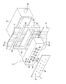
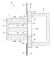
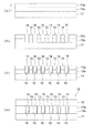
図1は、本発明のインクジェットヘッドの一例を示す分解斜視図であり、図2はその断面図である。図1、2において、Hはインクジェットヘッド、1は圧力室基板(ヘッドチップともいう)、2はヘッドチップ1の前面に接合されるノズルプレート、3はヘッドチップ1の後面に接合される配線基板、4は配線基板3に接合されるFPC、5は配線基板3の後面に接合されるインクマニホールドである。
FIG. 1 is an exploded perspective view showing an example of the ink jet head of the present invention, and FIG. 2 is a sectional view thereof. 1 and 2, H is an ink jet head, 1 is a pressure chamber substrate (also referred to as a head chip), 2 is a nozzle plate bonded to the front surface of the
なお、本発明においては、ヘッドチップ1からインクが吐出される側の面を「前面」と定義し、その反対側の面のインクの入口側を「後面」と定義する。また、ヘッドチップ1を前面又は後面から見て、並設されるチャネルを挟んで上下に位置する外側面をそれぞれ「上面」及び「下面」と定義する。 In the present invention, the surface where ink is ejected from the head chip 1 is defined as “front surface”, and the ink inlet side on the opposite surface is defined as “rear surface”. Further, when the head chip 1 is viewed from the front surface or the rear surface, the outer surfaces positioned above and below the channels arranged in parallel are defined as “upper surface” and “lower surface”, respectively.
ヘッドチップ1は、圧電素子からなる駆動壁13とチャネル14とが交互に並設されている。チャネル14の形状は、両側壁が上面及び下面に対してほぼ垂直に立ち上がっており、そして互いに平行である。図2に示すように、ヘッドチップ1の前面及び後面にそれぞれ各チャネル14の出口142と入口141とが配置されると共に、各チャネル14は入口141から出口142に亘る長さ方向で大きさと形状がほぼ変わらないストレートタイプである。
In the head chip 1, drive
このヘッドチップ1において、各チャネル14は図示上下に2列となるチャネル列を有している。各チャネル列はそれぞれ6個のチャネル14からなるが、ヘッドチップ1中のチャネル列を構成するチャネル14の数は何ら限定されない。
In the head chip 1, each
本発明のインクジェットヘッドは、図2に示すインクジェットヘッドHの作製過程で、下記に説明する方法により作製されるヘッドチップ1において、ヘッドチップ1を構成するチャネル(圧力室)14内に設けられた駆動電極15から引き出され、その駆動電極15と電気的に接続するための接続電極16と、圧力室14の入口141側にある配線基板3上に設けら、接続電極16に電圧を印可する配線電極33とを、本発明に係る光硬化性と熱硬化性を併せ持つ接着剤(以下、光・熱硬化型接着剤ともいう)で貼り合わせを行うことを特徴とする。
The inkjet head of the present invention is provided in a channel (pressure chamber) 14 constituting the head chip 1 in the head chip 1 manufactured by the method described below in the process of manufacturing the inkjet head H shown in FIG. A
また、本発明のインクジェットヘッドの作製方法においては、ヘッドチップ1の駆動電極15と接合させる配線基板3上に設けた配線電極33表面に、本発明に係る光・熱硬化型接着剤を塗設する工程と、ヘッドチップ1の位置を決めて、接着剤を塗設した配線電極33を有する配線基板3に貼合する工程と、配線基板3の接着面とは反対側の面であるインクの入口側141から光を照射して、本発明に係る光・熱硬化型接着剤を光硬化する工程と、次いで加熱処理を施して、光・熱硬化型接着剤を熱硬化する工程とを経て製造することを特徴とする。
In the method of manufacturing the ink jet head of the present invention, the photo / thermosetting adhesive according to the present invention is applied to the surface of the
また、他の本発明に係る光・熱硬化型接着剤の硬化方法としては、配線基板3の接着面の周囲から光を照射して、本発明に係る光・熱硬化型接着剤を光硬化した後、加熱処理を施して熱硬化する工程とを経て製造することも特徴の一つとする。
As another method for curing the light / thermosetting adhesive according to the present invention, the light / thermosetting adhesive according to the present invention is photocured by irradiating light from around the bonding surface of the
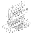
具体的なインクジェットヘッドの作製方法について、更に図3を用いて説明する。 A specific method for manufacturing the ink jet head will be further described with reference to FIGS.
図3は、インクジェットヘッドの構成の一例を示す分解斜視図である。 FIG. 3 is an exploded perspective view showing an example of the configuration of the inkjet head.
ヘッドチップ1は、複数の溝を有する圧電体101と蓋材102を接合して形成される。圧電体101の溝の表面は、図3において斜線で示した駆動電極15が形成されている。駆動電極15は、インクによる腐食を防止する目的で、透明な絶縁層により被覆されていることが好ましい。
The head chip 1 is formed by bonding a
ヘッドチップ1の後面には、各圧力室14の駆動電極15から引き出された接続電極16(電圧印加用電極)が形成されている。接続電極16の形成は、蒸着又はスパッタリングによって行うことができる。
On the rear surface of the head chip 1, connection electrodes 16 (voltage application electrodes) drawn from the
ノズルプレートは、ヘッドチップ1の各圧力室14の出口に対応する位置にそれぞれノズル21が開設されており、接続電極16が形成されたヘッドチップ1の前面に、例えば、本発明に係る光・熱硬化型接着剤を用いて接合される。従って、各圧力室14の入口、出口及びノズル21が直線状に配置される。
The nozzle plate is provided with
配線基板3は、ヘッドチップ1の各駆動電極15に図示しない駆動回路からの駆動電圧を印加する配線を接続するための板状の部材である。この配線基板3に用いられる基板には、非分極のPZTやAlN−BN、AlN等のセラミックス材料からなる基板、低熱膨張のプラスチックやガラスからなる基板、ヘッドチップ1に使用されている圧電体の基板材料と同一の基板材料を脱分極した基板等を用いることができる。好ましくは、熱膨張率の差に起因するヘッドチップ1の歪み等の発生を抑えるため、未分極のPZTを基準にして±3ppm以内の熱膨張係数の差を持つ材料を選定することである。
The
さらに光重合開始剤が感じる光を透過する材料が配線基板の接着面とは反対側から光照射したときに熱硬化前に接着部分の広い領域の硬化が進み、電極接続部分の位置ずれが更に抑制されることで好ましい。 Furthermore, when the light-transmitting material felt by the photopolymerization initiator is irradiated with light from the side opposite to the adhesive surface of the wiring board, curing of a wide area of the adhesive part proceeds before thermosetting, and the positional displacement of the electrode connection part further increases. It is preferable to be suppressed.
配線基板3を構成する基板は1枚板状のものに限らず、薄板状の基板材料を複数枚積層して所望の厚みとなるように形成してもよい。
The substrate constituting the
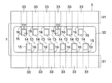
この配線基板3は、ヘッドチップ1の後面よりも大きな面積を有しており、ヘッドチップ1の圧力室14の並び方向(圧力室列方向)と直交する方向(図中のB方向)に延び、ヘッドチップ1からそれぞれ大きく張り出しており、各張り出し端が図示しないFPC等を接続するための配線接続部33となっている。また、配線基板3は、ヘッドチップ1の圧力室14の並び方向(図中のA方向)にもそれぞれ大きく張り出している。
The
配線基板3のほぼ中央部には開口部32が貫通形成されている。この開口部32は、ヘッドチップ1の後面に臨む全圧力室14の入口側を露呈させることができる程度の大きさに形成されている。
An
開口部32の形成方法としては、基板材料に応じて、ダイシングソーで加工する方法、超音波加工機で加工する方法、焼結前のセラミックスを型成形し、焼成する方法、サンドブラストにより形成する方法等が採用できる。
As a method for forming the
配線基板3のヘッドチップ1との接合面側となる表面に、ヘッドチップ1の後面に形成された各接続電極16と同数及び同ピッチ(W1+W2)で配線電極33(電圧印加用電極)が形成され、開口部32の周縁から各配線接続部31、31に延び、配線基板3の外縁まで至っている。この配線電極33は、FPC等が接合される際、FPC等に形成されている各配線と電気的に接続し、駆動回路からの駆動電圧を接続電極14を介して圧力室12内の駆動電極15に印加するための電極として機能する。
Wiring electrodes 33 (voltage application electrodes) are formed on the surface of the
なお、配線基板3の表面には、配線電極33の他に、ヘッドチップ1を位置決めするための位置決め用パターン38が形成されている。この位置決め用パターン38は、ヘッドチップ1との接合時にはヘッドチップ1の後面に形成された位置決め用パターン39と嵌合し、ヘッドチップ1の位置決めを行う際に使用される。
In addition to the
本発明において、このようにして形成されたヘッドチップ1と配線基板3の接合方法としては、はじめに、配線基板3のヘッドチップ1との接着部分(配線電極33の一部)に本発明に係る光・熱硬化型接着剤をディスペンサーで塗布する。次いで、配線基板3の配線電極33と、図4に記載のヘッドチップ1の接続電極16とが電気的に接続すると共に開口部32がヘッドチップ1の全チャネルを露呈させるように位置あわせをしながら、ヘッドチップ1と配線基板3を圧着する。
In the present invention, as a method of bonding the head chip 1 and the
次いで、配線基板3がガラスのように光透過性の場合は、高圧水銀灯を配線基板3の接着部の周辺から、例えば、5000mJ/cm2照度で照射する。また、配線基板3が光不透過性の材料から構成されている場合には、ヘッドチップのインク出口側142から、例えば、高圧水銀灯を5000mJ/cm2照射条件で照射する。更に、ヘッドチップ1と配線基板3を接合した周囲に高圧水銀灯を照射する。この様な光照射により、光硬化を行った後、所定の温度及び時間で加熱処理を行い熱硬化を施す。この工程においては、何れも構成部材も光硬化により固定されているので、圧着治具をはずしても加熱硬化ができる。
Next, when the
接着剤の光硬化に用いる照射光源としては、特定の波長領域の紫外線を安定した露光エネルギーで発光する紫外線ランプ及び特定の波長の紫外線を透過するフィルターを備えて構成される光源が好ましい。紫外線ランプとしては、水銀ランプ、メタルハライドランプ、エキシマーレーザー、紫外線レーザー、冷陰極管、熱陰極管、ブラックライト、LED(light emitting diode)等が適用可能であり、特に波長365nmの紫外線を発光する高圧水銀ランプが好ましい。 As the irradiation light source used for photocuring of the adhesive, a light source including an ultraviolet lamp that emits ultraviolet light in a specific wavelength region with stable exposure energy and a filter that transmits ultraviolet light of a specific wavelength is preferable. As the ultraviolet lamp, a mercury lamp, a metal halide lamp, an excimer laser, an ultraviolet laser, a cold cathode tube, a hot cathode tube, a black light, an LED (light emitting diode), and the like are applicable, and in particular, a high pressure that emits ultraviolet light having a wavelength of 365 nm. A mercury lamp is preferred.
また、加熱処理方法としては、電気オーブンまたはインクジェット記録ヘッドに圧着して加熱することができる加熱具が好ましく、例えば、ホットプレート、リボンヒーター等が挙げられる。また、加熱処理時に、少なくとも圧電体部を冷却する手段として、アルミニウムブロックに冷水を循環させて冷却させる手段を併用することが好ましい。 Moreover, as a heat processing method, the heating tool which can be heated by crimping | bonding to an electric oven or an inkjet recording head is preferable, for example, a hot plate, a ribbon heater, etc. are mentioned. In addition, as a means for cooling at least the piezoelectric body portion during the heat treatment, it is preferable to use a means for circulating cold water through the aluminum block for cooling.
次いで、配線基板3の配線電極33の形成方法について、更に図を用いて説明する。
Next, a method for forming the
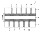
図5は、配線基板3の表面に導電性ペーストを用いて配線電極33をパターニングした状態を示す配線基板3の平面図である。このような導電性ペーストを用いた配線電極33のパターニングには、細密性とコスト安の両立が図り易い点でスクリーン印刷法が適している。また、その他、ディスペンサーやインクジェットを用いたパターニングを採用することもできる。
FIG. 5 is a plan view of the
本発明において用いられる導電性ペーストは、一般に導電剤としての金属粒子とバインダー樹脂の他、溶剤や増粘剤を含有する。金属粒子としては、特に制限はなく、一般にはAgを用いることができるが、その他、Au、Cu、AgPt、AgPtPd等を用いることもできる。 The conductive paste used in the present invention generally contains a solvent and a thickener in addition to metal particles and a binder resin as a conductive agent. There is no restriction | limiting in particular as a metal particle, Generally Ag can be used, However, Au, Cu, AgPt, AgPtPd etc. can also be used besides.
本発明において、ヘッドチップ1と配線基板3とは、配線基板3表面にこのようにして導電性ペーストを用いて配線電極33をパターニングした後、焼成処理を行った後、図6に示す様に配線電極33a部分に微量の金属粒子を含む導電性を有する本発明に係る光・熱硬化型接着剤を塗設した後、ヘッドチップ1の接続電極16と各配線電極33とを位置合わせした後、そのまま密着させ、その後に光照射処理及び加熱処理により硬化させる。この硬化処理により、同時にヘッドチップ1と配線基板3とが接着されて接合される。
In the present invention, the head chip 1 and the
なお、配線電極33を導電性ペーストを用いてパターニングする際、図5に示すように、配線電極33におけるヘッドチップ1の各接続電極16と接合される部位33aをその他の部位33bよりも細く形成することが好ましい。これにより、ヘッドチップ1と配線基板3とを密着させた際に、接続電極16と接合される部位33aが押し潰されて若干横に広がっても、隣接する配線33との電気的短絡を防ぐことができる。
When patterning the
図7、図8は、上記ヘッドチップ1を作製する方法の一例を示す概略断面図である。 7 and 8 are schematic cross-sectional views showing an example of a method for manufacturing the head chip 1.
図7の(a)に示す様に、はじめに、1枚のベース基板11上に、2枚の圧電素子基板13a、13bをそれぞれエポキシ系接着剤を用いて接合する。各圧電素子基板13a、13bに用いられる圧電材料としては、電圧を加えることにより変形を生じる公知の圧電材料を用いることができるが、特に、チタン酸ジルコン酸鉛(PZT)が好ましい。2枚の圧電素子基板13a、13bは互いに分極方向(矢印で示す)を反対方向に向けて積層し、基板11にエポキシ系接着剤接着剤を用いて接着する。
As shown in FIG. 7A, first, two
次いで、図7の(b)に示す様に、その2枚の圧電素子基板13a、13bに亘って、ダイシングソー等を用いて複数の平行な溝を研削する。これにより、ベース基板11上に高さ方向で分極方向が反対となる圧電素子からなる駆動壁13が並設される。各溝は圧電素子基板13a、13bの一方の端から他方の端に亘ってほぼ同じ一定の深さで研削することで、長さ方向で大きさと形状がほぼ変わらないストレート状のチャネル14となる。
Next, as shown in FIG. 7B, a plurality of parallel grooves are ground using a dicing saw or the like over the two
また、図示しないが、ベース基板11を用いる代わりに圧電素子基板13bを厚手のものとし、薄手の圧電素子基板13a側から厚手の圧電素子基板13bの中途部にまで至る複数の平行な溝を研削することにより、高さ方向で分極方向が反対となる駆動壁13の形成と同時にベース基板11の部分が圧電素子基板13bによって一体に形成されるようにしてもよい。
Although not shown, instead of using the
次いで、このようにして形成した各チャネル14の内面に駆動電極15を形成する。駆動電極15を形成する金属は、Ni、Co、Cu、Al等があり、電気抵抗の面からはAlやCuを用いることが好ましいが、腐食や強度、コストの面からNiが好ましく用いられる。また、Alの上に更にAuを積層した積層構造としてもよい。
Next, the
駆動電極15の形成は、蒸着法、スパッタリング法、めっき法、CVD(化学気相反応法)等の真空装置を用いた方法等によって金属被膜を形成する方法が挙げられるが、めっき法によるものが好ましく、特に無電解めっきにより形成することが好ましい。無電解めっきによれば、均一且つピンホールフリーの金属被膜を形成することができる。めっき膜の厚みは0.5〜5μmの範囲が好ましい。
Examples of the formation of the
次いで、図7の(c)に示す様に、駆動電極15はチャネル14毎に独立させる必要があるため、駆動壁13の上端面には金属被膜が形成されないようにする。このため、例えば各駆動壁13の上端面に予めドライフィルムを貼着したり、レジストを形成しておき、金属被膜を形成した後に除去することで、各駆動壁13の側面及び各チャネル14の底面に選択的に駆動電極15を形成するとよい。
Next, as shown in FIG. 7C, the
次いで、図7の(d)に示す様に、このようにして駆動電極15を形成した後、駆動壁13の上端面にカバー基板12をエポキシ系接着剤を用いて接合し、1列のチャネル列を有するヘッド基板10を作製する。ベース基板11及びカバー基板12には、駆動壁13を構成する圧電材料と同一の基板材料を脱分極して用いると、基板接着時の加熱や駆動の熱の影響による、熱膨張係数の差に起因する速度分布や駆動特性のばらつきを少なくすることができる。
Next, as shown in FIG. 7D, after the
また、このようなヘッド基板は、図7の(d)に示すようにして作製されるものに限らず、図8に示すように、ベース基板11を用いる代わりに圧電素子基板を厚手のものとして、平行な溝を研削して駆動壁13とチャネル14とを交互に並設し、各チャネル14の内面に駆動電極15を形成したものを2組(上側基板10aと下側基板10b)用意し、これを駆動壁13同士が相対するように接着することで、図7の(d)と類似のヘッド基板10Aとすることもできる。この場合、図7の(a)のように薄い圧電素子基板13aを圧電素子基板13b上に接着する必要がないのでコスト上有利である。但し、以下では、図7の(d)のヘッド基板10を用いて作製する場合について説明する。
Further, such a head substrate is not limited to the one manufactured as shown in FIG. 7D, but instead of using the
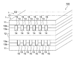
図7の(d)に示すようにして作製されたヘッド基板10を2枚用い、図9に示すように互いのカバー基板12同士を重ね合わせ、エポキシ系接着剤を用いて接合することで、上下で2列のチャネル列を有する積層ヘッド基板100を作製した後、この積層ヘッド基板100を、チャネル14の長さ方向と直交する方向に沿う複数のカットラインC1、C2・・・に沿って切断することにより、ハーモニカ型の複数のヘッドチップ1、1・・・を作製する。
By using two
このようにして作製されるヘッドチップ1、1・・・は、各チャネル列において圧電素子からなる駆動壁13とチャネル14とが交互に並設される。チャネル14の形状は、両側壁がヘッドチップ1のベース基板11からほぼ垂直方向に立ち上がっており、そして互いに平行である。ヘッドチップ1の前面及び後面には、それぞれ各チャネル14の出口142と入口141とが配置される。各チャネル14は、入口から出口に亘る長さ方向で大きさと形状がほぼ変わらないストレートタイプとなる。
In the head chips 1, 1... Thus manufactured, drive
このようなハーモニカ型のヘッドチップ1では、各チャネル14内の駆動電極15に駆動回路からの駆動電圧を印加するためのFPC等の配線を外部から接続できるようにするため、各駆動電極15をヘッドチップ1の外面にまで引き出す必要がある。そこで、次に、ヘッドチップ1の後面に、駆動電極15のうちのチャネル14の底面に形成された部分(チャネル14内に臨むベース基板11の表面)からベース基板11の後端面にかけて接続電極16を引き出し形成する。
In such a harmonica type head chip 1, each
図10は、ヘッドチップ1の外面に、各駆動電極15と電気的に接続する接続電極16を引き出し形成する方法の一例を説明する説明図である。
FIG. 10 is an explanatory diagram for explaining an example of a method of drawing out and forming
接続電極16は、図10の(a)に示すように、ヘッドチップ1の後面に、駆動電極15のうちのチャネル14内に臨むベース基板11表面に形成された部分を少なくとも含み、ヘッドチップ1の上面側及び下面側にかけて開設された開口部201を有する感光性ドライフィルム200を貼着し、Al等の電極形成用の金属を蒸着して、開口部201内に金属被膜を生成することによって形成することができる。
As shown in FIG. 10A, the
チャネル14内の駆動電極15と接続電極16をスムーズに接続するためには、蒸着方向に対してヘッドチップ1の後面を垂直にするのではなく、所定の角度傾けて蒸着することが望ましい。具体的には、蒸着方向(金属粒子が飛来する方向)が、図10の(a)の紙面に垂直ではく、垂直から上側及び下側に30〜60度程度傾いていることが望ましい。
In order to smoothly connect the
また、接続電極16は、Alの金属被膜の上に更にAuを蒸着する等の方法によって積層構造としてもよい。更に、接続電極16の形成は、蒸着に代えてスパッタリングによって行うようにしてもよい。
Further, the
特に、ヘッドチップ1を図8に示すように作製したヘッド基板10Aを用いて切断加工した場合、上側基板10aの駆動電極15と下側基板10bの駆動電極15は、間に接着剤が存在するので電気的に接続されていない。このため、感光性ドライフィルム200の開口部201内に金属被膜を形成する際に、この2つの駆動電極15、15が接続されるようにする必要がある。これは電極形成を蒸着で行う場合は、蒸着方向を所定の方向に複数回行うか、または蒸着中に基板の方向を変化させることにより実現できる。スパッタリングで電極形成する際は、金属粒子が種々の方向より飛来するので特に基板の向きを変えなくても2つの駆動電極15、15の接続をとることができる。
In particular, when the head chip 1 is cut using the
なお、開口部201は、感光性ドライフィルム200の現像工程・水洗工程での作業性を考え、チャネル14の全面において開口していることが望ましい。全面において開口していることにより、チャネル14内の現像液、洗浄水の除去が容易となる。
Note that the
この後、感光性ドライフィルム200を除去すると、図10の(b)に示すように、ヘッドチップ1の後面に、各チャネル14から駆動電極15と電気的に接続する接続電極16がチャネル14毎に独立して引き出される。
Thereafter, when the photosensitive
ノズルプレート2は、ヘッドチップ1の各チャネル14に対応する位置にそれぞれノズル21が開設されており、接続電極16が形成されたヘッドチップ1の前面に本発明に係る光・熱硬化性のエポキシ系接着剤を用いて接合することが好ましい。
The nozzle plate 2 is provided with
配線基板3はヘッドチップ1の駆動電極15に図示しない駆動回路から駆動電圧を印加する配線を接続するための板状の部材である。この配線基板3に用いられる材料はPZT、AlN−BN、AlNなどのセラミックス、ガラス、および低熱膨張率のプラスチックを用いることが出来る。好ましくは光透過性の材料が好ましく、ガラスが更に好ましい。
The
この配線基板3は、チャネル14の並び方向においてヘッドチップ1と同一またはそれ以上の幅を有すると共に、ヘッドチップ1のチャネル14の並び方向(チャネル列方向)と直交する方向(図1、図2における上下方向)に延び、ヘッドチップ1の上面及び下面からそれぞれ大きく張り出しており、各張り出し端がFPC4、4を接続するための配線接続部33となっている。
The
また、配線基板3のほぼ中央部には開口部32が貫通形成されている。この開口部32は、ヘッドチップ1の全チャネル14の入口141側を露呈させることができる程度の大きさに形成されている。従って、図11に示すように、ヘッドチップ1の後面に配線基板3を接合した状態で、この開口部32を通して、ヘッドチップ1の全駆動壁13、全チャネル14及び全駆動電極15を覗くことができるようになっている。
In addition, an
開口部32の形成方法としては、基板材料に応じて、ダイシングソーで加工する方法、超音波加工機で加工する方法、焼結前のセラミックスを型成形し、焼成する方法、またはサンドブラストにより形成する方法等が採用できる。
As a method of forming the
配線基板3のヘッドチップ1との接合面側となる表面に、ヘッドチップ1の後面に形成された各接続電極16と同数及び同ピッチで配線電極33が形成され、各配線接続部31、31まで延びている。この配線電極33は、FPC4が接合される際、FPC4に形成されている各配線41と電気的に接続し、FPC4の配線41を介して供給される駆動回路からの駆動電圧を、接続電極16を介してチャネル14内の駆動電極15に印加するための電極として機能する。
配線電極33の形成は、配線基板3の表面にスピンコート法によりポジレジストをコーティングし、その後、このポジレジストをストライプ状のマスクを用いて露光し、現像することにより、ストライプ状のポジレジストの間に接続電極16と同数及び同ピッチで配線基板3の表面を露呈させ、その表面に、蒸着法やスパッタリング法等によって電極形成用の金属によって金属被膜を形成することにより行うことができる。電極形成用の金属としては、接続電極16と同一のものを使用することができる。
The
《光硬化性と熱硬化性を併せ持つ接着剤》
本発明に係る光硬化性と熱硬化性を併せ持つ接着剤としては、特に制限はないが、重合性モノマーとしてエポキシモノマーを含有し、かつ重合開始剤として光重合開始剤及び熱重合開始剤を含有する接着剤であることが好ましい。
<< Adhesive with both photocuring and thermosetting >>
The adhesive having both photocurability and thermosetting according to the present invention is not particularly limited, but contains an epoxy monomer as a polymerizable monomer, and contains a photopolymerization initiator and a thermal polymerization initiator as a polymerization initiator. It is preferable to be an adhesive.
(重合性モノマー)
一般に、光・熱重合性モノマーとしては、ラジカル重合型モノマーとカチオン重合型モノマーが挙げられるが、本発明においては、インクに対する耐性が高く、転写性に優れたカチオン重合型モノマーが好ましい。カチオン重合型モノマーとしては、各種公知のカチオン重合性モノマーを挙げることができ、例えば、オキセタン環を有する化合物、エポキシ化合物、ビニルエーテル化合物等を挙げることができるが、その中でもエポシキモノマーを用いることが好ましい。
(Polymerizable monomer)
In general, examples of the photo / thermopolymerizable monomer include a radical polymerizable monomer and a cationic polymerizable monomer. In the present invention, a cationic polymerizable monomer having high resistance to ink and excellent transferability is preferable. Examples of the cationic polymerization type monomer include various known cationic polymerizable monomers, and examples include compounds having an oxetane ring, epoxy compounds, vinyl ether compounds, etc. Among them, it is preferable to use epoxy monomers. .
本発明に係る接着剤に適用可能なエポキシ化合物としては、エポキシ基を有する化合物のモノマー及びそのオリゴマーのいずれも使用できる。具体的には、従来公知の芳香族エポキシ化合物、脂環式エポキシ化合物及び脂肪族エポキシ化合物が挙げられる。なお、以下エポキシ化合物とは、モノマーまたはそのオリゴマーを意味する。 As an epoxy compound applicable to the adhesive according to the present invention, any of a monomer of an epoxy group-containing compound and an oligomer thereof can be used. Specific examples include conventionally known aromatic epoxy compounds, alicyclic epoxy compounds, and aliphatic epoxy compounds. Hereinafter, the epoxy compound means a monomer or an oligomer thereof.
芳香族エポキシ化合物として好ましいものは、少なくとも1個の芳香族核を有する多価フェノールあるいはそのアルキレンオキサイド付加体とエピクロルヒドリンとの反応によって製造されるジまたはポリグリシジルエーテルであり、例えば、ビスフェノールAあるいはそのアルキレンオキサイド付加体のジまたはポリグリシジルエーテル、水素添加ビスフェノールAあるいはそのアルキレンオキサイド付加体のジまたはポリグリシジルエーテル、ならびにノボラック型エポキシ樹脂等が挙げられる。ここでアルキレンオキサイドとしては、エチレンオキサイド及びプロピレンオキサイド等が挙げられる。 A preferable aromatic epoxy compound is a di- or polyglycidyl ether produced by the reaction of a polyhydric phenol having at least one aromatic nucleus or an alkylene oxide adduct thereof and epichlorohydrin, for example, bisphenol A or its Examples thereof include di- or polyglycidyl ethers of alkylene oxide adducts, hydrogenated bisphenol A or di- or polyglycidyl ethers of alkylene oxide adducts thereof, and novolak-type epoxy resins. Here, examples of the alkylene oxide include ethylene oxide and propylene oxide.
脂環式エポキシ化合物としては、少なくとも1個のシクロヘキセンまたはシクロペンテン環等のシクロアルカン環を有する化合物を、過酸化水素、過酸等の適当な酸化剤でエポキシ化することによって得られるシクロヘキセンオキサイドまたはシクロペンテンオキサイド含有化合物が好ましく、具体例としては、以下に示す化合物等が挙げられる。 As the alicyclic epoxy compound, cyclohexene oxide or cyclopentene obtained by epoxidizing a compound having at least one cycloalkane ring such as cyclohexene or cyclopentene ring with an appropriate oxidizing agent such as hydrogen peroxide or peracid. Oxide-containing compounds are preferred, and specific examples include the compounds shown below.
脂肪族エポキシ化合物の好ましいものとしては、脂肪族多価アルコールあるいはそのアルキレンオキサイド付加体のジまたはポリグリシジルエーテル等があり、その代表例としては、エチレングリコールのジグリシジルエーテル、プロピレングリコールのジグリシジルエーテルまたは1,6−ヘキサンジオールのジグリシジルエーテル等のアルキレングリコールのジグリシジルエーテル、グリセリンあるいはそのアルキレンオキサイド付加体のジまたはトリグリシジルエーテル等の多価アルコールのポリグリシジルエーテル、ポリエチレングリコールあるいはそのアルキレンオキサイド付加体のジグリシジルエーテル、ポリプロピレングリコールあるいはそのアルキレンオキサイド付加体のジグリシジルエーテル等のポリアルキレングリコールのジグリシジルエーテル等が挙げられる。ここでアルキレンオキサイドとしては、エチレンオキサイド及びプロピレンオキサイド等が挙げられる。 Preferred examples of the aliphatic epoxy compound include di- or polyglycidyl ethers of aliphatic polyhydric alcohols or alkylene oxide adducts thereof, and typical examples thereof include diglycidyl ether of ethylene glycol and diglycidyl ether of propylene glycol. Or polyglycidyl ether of polyhydric alcohol such as diglycidyl ether of alkylene glycol such as diglycidyl ether of 1,6-hexanediol, glycerin or alkylene oxide adduct thereof, polyethylene glycol or alkylene oxide thereof Diglycidyl ether, poly (alkylene glycol) such as polypropylene glycol or diglycidyl ether of alkylene oxide adducts thereof Include diglycidyl ether of. Here, examples of the alkylene oxide include ethylene oxide and propylene oxide.
更に、これらの化合物の他に、分子内に1個のオキシラン環を有するモノマーである脂肪族高級アルコールのモノグリシジルエーテル及びフェノール、クレゾールのモノグリシジルエーテル等も用いることができる。 In addition to these compounds, monoglycidyl ethers of aliphatic higher alcohols and monoglycidyl ethers of phenol and cresol, which are monomers having one oxirane ring in the molecule, can also be used.
本発明においては、エポキシモノマーとしては、脂環式エポキシ化合物、ビスフェノールA型エポキシ化合物、ビスフェノールF型エポキシ化合物等が好ましく、その中でも、特に脂環式エポキシ化合物が好ましく、中でも、3,4−エポキシシクロヘキシルカルボン酸−3′,4′−エポキシシクロヘキシルメチルが低温環境下の硬化が速く好ましい。特に、圧電体を使用するヘッドでは脱分極を生じさせないために硬化温度は100℃以下が好ましいので、硬化速度の速い脂環式エポキシモノマーが好ましい。 In the present invention, the epoxy monomer is preferably an alicyclic epoxy compound, a bisphenol A type epoxy compound, a bisphenol F type epoxy compound or the like, among which an alicyclic epoxy compound is particularly preferable, and among these, 3,4-epoxy Cyclohexylcarboxylic acid-3 ', 4'-epoxycyclohexylmethyl is preferred because it cures quickly in a low temperature environment. In particular, in a head using a piezoelectric body, the curing temperature is preferably 100 ° C. or lower in order not to cause depolarization. Therefore, an alicyclic epoxy monomer having a high curing rate is preferable.
これらの脂環式エポキシ化合物は、その製法は問わないが、例えば、丸善KK出版、第四版実験化学講座20有機合成II、213〜、平成4年、Ed.by Alfred Hasfner,The chemistry of heterocyclic compounds−Small Ring Heterocycles part3 Oxiranes,John&Wiley and Sons,An Interscience Publication,New York,1985、吉村、接着、29巻12号、32、1985、吉村、接着、30巻5号、42、1986、吉村、接着、30巻7号、42、1986、特開平11−100378号、特許2906245号、特許2926262号の各公報等の文献を参考にして合成できる。 These alicyclic epoxy compounds may be produced by any method. For example, Maruzen KK Publishing, 4th Edition Experimental Chemistry Course 20 Organic Synthesis II, 213, 1992, Ed. By Alfred Hasfner, The Chemistry of Heterocyclic Compounds-Small Ring Heterocycles part3, Oxilanes, John & Wiley and Sons, An Interc. 42, 1986, Yoshimura, Adhesion, Vol. 30, No. 7, 42, 1986, Japanese Patent Application Laid-Open No. 11-1000037, Japanese Patent No. 2906245, Japanese Patent No. 2926262, and the like.
(光重合開始剤)
本発明において、カチオン重合性モノマーを光重合させるためのカチオン性光重合開始剤(光重合開始剤)としては、公知のあらゆる光酸発生剤を用いることができる。光酸発生剤としては、例えば、化学増幅型フォトレジストや光カチオン重合に利用される化合物が用いられる(有機エレクトロニクス材料研究会編、「イメージング用有機材料」、ぶんしん出版(1993年)、187〜192ページ参照)。
(Photopolymerization initiator)
In the present invention, any known photoacid generator can be used as the cationic photopolymerization initiator (photopolymerization initiator) for photopolymerizing the cationic polymerizable monomer. As the photoacid generator, for example, a chemically amplified photoresist or a compound used for photocationic polymerization is used (edited by Organic Electronics Materials Research Group, “Organic Materials for Imaging”, Bunshin Publishing (1993), 187. To page 192).
第1に、ジアゾニウム、アンモニウム、ヨードニウム、スルホニウム、ホスホニウムなどの芳香族オニウム化合物のB(C6F5)4 -、PF6 -、AsF6 -、SbF6 -、CF3SO3 -塩を挙げることができ、第2にスルホン酸を発生するスルホン化物を挙げることができ、第3にハロゲン化水素を光発生するハロゲン化物も用いることができ、第4に鉄アレン錯体を挙げることができる。例えば、ジアリルヨードニウムやトリアリルスルホニウムのヘキサフルオロホスフェート、ヘキサフルオロアンチモネートまたはペンタフルオロフェニルボレート塩などが挙げられ、イルガキュア−261(チバガイギー社製)、SP−150、SP−170(以上、旭電化社製)、PI2074やUVI−6992(ダウケミカル製)などの商品名で市販されている。 First, B (C 6 F 5 ) 4 − , PF 6 − , AsF 6 − , SbF 6 − , CF 3 SO 3 − salt of aromatic onium compounds such as diazonium, ammonium, iodonium, sulfonium, phosphonium, etc. Secondly, sulfonates that generate sulfonic acid can be mentioned, thirdly, halides that generate hydrogen halide can also be used, and fourthly, iron allene complexes can be mentioned. Examples include hexafluorophosphate, hexafluoroantimonate or pentafluorophenyl borate salt of diallyl iodonium or triallyl sulfonium, Irgacure-261 (manufactured by Ciba Geigy), SP-150, SP-170 (above, Asahi Denka Co., Ltd.) ), PI2074, and UVI-6992 (manufactured by Dow Chemical).
(熱重合開始剤)
本発明において、カチオン重合性モノマーを熱重合させるためのカチオン性熱重合開始剤(光重合開始剤)としては、好ましく、特に10〜150℃の温度でカチオンを発生する化合物が好ましい。具体的には、オニウム塩を挙げることができる。このオニウム塩として、周期表第Va族元素の塩、例えば、ホスホニウム塩(例えば、ヘキサフルオロリン酸トリフェニルフェナシルホスホニウムなど)、第VIa族元素の塩、例えば、スルホニウム塩(例えば、テトラフルオロホウ酸トリフェニルスルホニウム、ヘキサフルオロリン酸トリフェニルスルホニウム、ヘキサフルオロリン酸トリス(4−チオメトキシフェニル)スルホニウム、およびヘキシサフルオロアンチモン酸トリフェニルスルホニウムなど)、第VIIa族元素の塩、例えば、ヨードニウム塩(例えば、塩化ジフェニルヨードニウムなど)、及びフッ化ホウ素アニリン錯体、三フッ化ホウ素モノエチルアミン錯体、トリアルキルスルホニウムアンチモンネートなどが挙げられる。中でも、脂肪族炭化水素を置換基とするオニウム塩が好ましい。
(Thermal polymerization initiator)
In the present invention, the cationic thermal polymerization initiator (photopolymerization initiator) for thermally polymerizing the cationic polymerizable monomer is preferably a compound that generates a cation at a temperature of 10 to 150 ° C. Specific examples include onium salts. Examples of the onium salts include salts of Group Va elements of the periodic table, such as phosphonium salts (for example, triphenylphenacylphosphonium hexafluorophosphate), salts of Group VIa elements, such as sulfonium salts (for example, tetrafluoroborates). Triphenylsulfonium acid, triphenylsulfonium hexafluorophosphate, tris (4-thiomethoxyphenyl) sulfonium hexafluorophosphate, and triphenylsulfonium hexahexafluoroantimonate), salts of Group VIIa elements such as iodonium salts (For example, diphenyliodonium chloride), boron fluoride aniline complex, boron trifluoride monoethylamine complex, trialkylsulfonium antimonate and the like. Among these, an onium salt having an aliphatic hydrocarbon as a substituent is preferable.
このような芳香族オニウム塩をエポキシ化合物の重合におけるカチオン熱重合開始剤として使用することは、米国特許第4,058,401号、同第4,069,055号、同第4,101,513号および同第4,161,478号公報に詳述されている。又特開2000−10271号、機能材料(1995年5月号Vol.13,No.5 P.5〜11)記載等の熱酸発生剤を用いることもできる。 The use of such an aromatic onium salt as a cationic thermal polymerization initiator in the polymerization of an epoxy compound is disclosed in U.S. Pat. Nos. 4,058,401, 4,069,055, and 4,101,513. No. and No. 4,161,478. Further, thermal acid generators such as those described in JP-A No. 2000-10271 and functional materials (May 1995, Vol. 13, No. 5 P. 5 to 11) can also be used.
具体的には、三新化学工業株式会社製サンエイドSIシリーズのサンエイドSI−60L(熱カチオン発生温度90℃)、SI−80L(熱カチオン発生温度110℃)、SI−100L(熱カチオン発生温度120℃)、みどり化学株式会社製、NDI105(熱カチオン発生温度100℃)、NB−101(熱カチオン発生温度110℃)等を使用できる。
Specifically, San-Aid SI-60L (thermal cation generation temperature 90 ° C.), SI-80L (thermal cation generation temperature 110 ° C.), SI-100L (thermal cation generation temperature 120) of San-Aid SI series manufactured by Sanshin Chemical Industry Co., Ltd. ° C), manufactured by Midori Chemical Co., Ltd., NDI105 (thermal
これら各重合開始剤の添加量としては、接着剤の固形分中に0.1〜30質量%添加することが好ましく、より好ましくは0.2〜10質量%である。 As addition amount of each of these polymerization initiators, it is preferable to add 0.1-30 mass% in solid content of an adhesive agent, More preferably, it is 0.2-10 mass%.
接着剤に含有される導電性微粒子は、金属微粒子や金属により被覆された非金属微粒子が挙げられる。中でも断線が生じにくい点でニッケル微粒子が好ましい。 Examples of the conductive fine particles contained in the adhesive include metal fine particles and non-metallic fine particles coated with metal. Among these, nickel fine particles are preferable in that disconnection hardly occurs.
以下、実施例を挙げて本発明を具体的に説明するが、本発明はこれらに限定されるものではない。なお、実施例において「部」あるいは「%」の表示を用いるが、特に断りがない限り「質量部」あるいは「質量%」を表す。 EXAMPLES Hereinafter, the present invention will be specifically described with reference to examples, but the present invention is not limited thereto. In addition, although the display of "part" or "%" is used in an Example, unless otherwise indicated, "part by mass" or "mass%" is represented.
実施例1
図1、図2、図3の構成からなるインクジェットヘッドを作製した。
Example 1
An ink jet head having the configuration shown in FIGS. 1, 2, and 3 was produced.
透明なガラス支持体からなる配線基板3のヘッドチップ1との接着部分に、図5、図6に記載の構成となる様に導電性ペーストをスクリーン印刷により形成及び焼結処理を行って、配線電極33を形成した。配線基板の熱膨張率とヘッドチップの熱膨張率の差は2%であった。次いで、形成した配線基板3のヘッドチップとの接合部分を被覆する様に、下記接着剤1をディスペンサーを用いて、厚さ5μmとなる条件で付与した。
A conductive paste is formed by screen printing and sintered on the bonding portion of the
次いで、接着剤1を付与した配線基板3の配線電極33と、図4に記載のヘッドチップ1の接続電極16とが電気的に接続すると共に開口部32がヘッドチップ1の全チャネルを露呈させるように位置あわせをしながら、ヘッドチップ1と配線基板3を圧着した。
Next, the
次いで、配線基板3から、インク入口側141にむけて、高圧水銀灯を用いて、2000mW/cm2の照度で10秒間照射した後、100℃で1時間の加熱処理を行って、ヘッドチップ1と配線基板3とを接合して、インクジェットヘッド1を作製した。
Next, irradiation was performed for 10 seconds at an illuminance of 2000 mW / cm 2 from the
(接着剤1の組成)
セロキサイド2021(脂環式エポキシ樹脂;ダイセルUCB社製) 50部
エピコート807(ビスフェノールF型エポキシ樹脂;ジャパンエポキシレジン製)
50部
アデカオプトマーSP−170(光カチオン重合開始剤;アデカ製) 2部
アデカオプトロンCP−77(熱カチオン重合開始剤;アデカ製) 0.4部
A−187(シランカップリング剤;日本ユニカー社製) 3部
ニッケル粒子(平均粒子径:3μm) 100部
上記作製したインクジェットヘッドは、チャネルへの接着剤の流れ込みは無かった。また、電極の断線やショートもなかった。
(Composition of adhesive 1)
Celoxide 2021 (alicyclic epoxy resin; manufactured by Daicel UCB) 50 parts Epicoat 807 (bisphenol F type epoxy resin; manufactured by Japan Epoxy Resin)
50 parts Adeka optomer SP-170 (photo cationic polymerization initiator; manufactured by Adeka) 2 parts Adeka Optron CP-77 (thermal cationic polymerization initiator; manufactured by Adeka) 0.4 part A-187 (silane coupling agent; Nippon Unicar) 3 parts Nickel particles (average particle size: 3 μm) 100 parts The inkjet head produced above had no flow of adhesive into the channel. Further, there was no disconnection or short circuit of the electrode.
上記作製したインクジェットヘッド1を用いて、溶剤顔料インクを用いて、1ヶ月間の連続出射を行った結果、ノズル欠の発生がなく、またヘッドチップ1と配線基板3の接着部を目視観察した結果、接着部の剥がれは、まったく認められなかった。
As a result of continuous emission for one month using the solvent pigment ink using the ink jet head 1 produced as described above, there was no nozzle shortage, and the adhesion part between the head chip 1 and the
実施例2
実施例1に記載のインクジェットヘッド1の作製において、2000mW/cm2の照度で10秒間の光照射を、インク入口側141を含めたヘッドチップ1と配線基板3の接合部周辺に行った以外は同様にして、インクジェットヘッド2を作製し、溶剤顔料インクを用いて、1ヶ月間の連続出射を行った結果、ノズル欠の発生がなく、またヘッドチップ1と配線基板3の接着部を目視観察した結果、接着部の剥がれは、まったく認められなかった。
Example 2
In the production of the inkjet head 1 described in Example 1, light irradiation for 10 seconds at an illuminance of 2000 mW / cm 2 was performed around the joint between the head chip 1 and the
比較例1
実施例1に記載の接着剤1の調製において、アデカオプトマーSP−170(光カチオン重合開始剤;アデカ製)を除き、アデカオプトロンCP−77(熱カチオン重合開始剤;アデカ製)の添加量を2.4部に変更した以外は同様にして接着剤2を調製した。
Comparative Example 1
In the preparation of the adhesive 1 described in Example 1, the addition amount of Adeka Optron CP-77 (Thermal Cationic Polymerization Initiator; manufactured by Adeka) except for Adekaoptomer SP-170 (Photo Cationic Polymerization Initiator; manufactured by Adeka) Adhesive 2 was prepared in the same manner except that was changed to 2.4 parts.
実施例1に記載のインクジェットヘッド1の作製において、接着剤1に代えて接着剤2を用いた以外は同様にして、インクジェットヘッド3を作製したが、接着剤によるチャネル詰まりが観察された。溶剤顔料インクを用いて、1ヶ月間の連続出射を行った結果、他のチャネルでもノズル欠の発生が認められ、またヘッドチップ1と配線基板3の接着部を目視観察した結果、接続電極16と配線基板の配線接続部33の間にズレが認められた。
In the production of the inkjet head 1 described in Example 1, the
比較例2
実施例1に記載の接着剤1の調製において、アデカオプトロンCP−77(熱カチオン重合開始剤;アデカ製)を除き、アデカオプトマーSP−170(光カチオン重合開始剤;アデカ製)の添加量を2.4部に変更した以外は同様にして接着剤3を調製した。
Comparative Example 2
In the preparation of the adhesive 1 described in Example 1, except for Adeka Optron CP-77 (thermal cationic polymerization initiator; manufactured by Adeka), an addition amount of Adeka optomer SP-170 (photo cationic polymerization initiator; manufactured by Adeka)
実施例1に記載のインクジェットヘッド1の作製において、接着剤1に代えて接着剤3を用いた以外は同様にして、インクジェットヘッド4を作製し、溶剤顔料インクを用いて、1ヶ月間の連続出射を行った結果、ノズル欠の発生が認められ、またヘッドチップ1と配線基板3の接着部を目視観察した結果、接着部に剥がれが認められた。
In the production of the inkjet head 1 described in Example 1, the inkjet head 4 was produced in the same manner except that the adhesive 3 was used in place of the adhesive 1, and the ink was continuously used for one month using the solvent pigment ink. As a result of the emission, the occurrence of a missing nozzle was observed. As a result of visual observation of the bonded portion between the head chip 1 and the
1 ヘッドチップ
10、10A ヘッド基板
11 ベース基板
12 カバー基板
13 駆動壁
13a、13b 圧電素子基板
14 チャネル
141 チャネルの入口
142 チャネルの出口
15 駆動電極
16 接続電極
2 ノズルプレート
21 ノズル
3 配線基板
31 配線接続部
32 開口部
33 配線電極
4 FPC
41 配線
5 インクマニホールド
H インクジェットヘッド
DESCRIPTION OF SYMBOLS 1
41
Claims (5)
Priority Applications (1)
| Application Number | Priority Date | Filing Date | Title |
|---|---|---|---|
| JP2008005494A JP2009166309A (en) | 2008-01-15 | 2008-01-15 | Inkjet head and method for manufacturing inkjet head |
Applications Claiming Priority (1)
| Application Number | Priority Date | Filing Date | Title |
|---|---|---|---|
| JP2008005494A JP2009166309A (en) | 2008-01-15 | 2008-01-15 | Inkjet head and method for manufacturing inkjet head |
Publications (1)
| Publication Number | Publication Date |
|---|---|
| JP2009166309A true JP2009166309A (en) | 2009-07-30 |
Family
ID=40968065
Family Applications (1)
| Application Number | Title | Priority Date | Filing Date |
|---|---|---|---|
| JP2008005494A Pending JP2009166309A (en) | 2008-01-15 | 2008-01-15 | Inkjet head and method for manufacturing inkjet head |
Country Status (1)
| Country | Link |
|---|---|
| JP (1) | JP2009166309A (en) |
Cited By (5)
| Publication number | Priority date | Publication date | Assignee | Title |
|---|---|---|---|---|
| JP2011116117A (en) * | 2009-12-04 | 2011-06-16 | Samsung Electro-Mechanics Co Ltd | Inkjet head package |
| JP2013014755A (en) * | 2011-06-10 | 2013-01-24 | Sekisui Chem Co Ltd | Anisotropic conductive material, connecting structure and method for producing connecting structure |
| JP2015051587A (en) * | 2013-09-06 | 2015-03-19 | コニカミノルタ株式会社 | Ink jet head and wiring board |
| WO2015190409A1 (en) * | 2014-06-12 | 2015-12-17 | コニカミノルタ株式会社 | Ink jet head and ink jet recording device |
| JP2021519536A (en) * | 2018-03-26 | 2021-08-10 | ソイテック | Method of transferring the piezoelectric layer onto the support substrate |
-
2008
- 2008-01-15 JP JP2008005494A patent/JP2009166309A/en active Pending
Cited By (8)
| Publication number | Priority date | Publication date | Assignee | Title |
|---|---|---|---|---|
| JP2011116117A (en) * | 2009-12-04 | 2011-06-16 | Samsung Electro-Mechanics Co Ltd | Inkjet head package |
| JP2013014755A (en) * | 2011-06-10 | 2013-01-24 | Sekisui Chem Co Ltd | Anisotropic conductive material, connecting structure and method for producing connecting structure |
| JP2015051587A (en) * | 2013-09-06 | 2015-03-19 | コニカミノルタ株式会社 | Ink jet head and wiring board |
| WO2015190409A1 (en) * | 2014-06-12 | 2015-12-17 | コニカミノルタ株式会社 | Ink jet head and ink jet recording device |
| JPWO2015190409A1 (en) * | 2014-06-12 | 2017-04-20 | コニカミノルタ株式会社 | Inkjet head and inkjet recording apparatus |
| EP3156234A4 (en) * | 2014-06-12 | 2018-01-24 | Konica Minolta, Inc. | Ink jet head and ink jet recording device |
| JP2021519536A (en) * | 2018-03-26 | 2021-08-10 | ソイテック | Method of transferring the piezoelectric layer onto the support substrate |
| JP7256204B2 (en) | 2018-03-26 | 2023-04-11 | ソイテック | A method for transferring a piezoelectric layer onto a supporting substrate |
Similar Documents
| Publication | Publication Date | Title |
|---|---|---|
| US7930824B2 (en) | Method of manufacturing ink jet recording head | |
| KR0152452B1 (en) | Manufacturing method of ink jet recording head | |
| JPS58220754A (en) | Ink jet recording head | |
| KR20070087163A (en) | Photosensitive laminate film for forming top plate portion of precision fine space and method of forming precision fine space | |
| US8158336B2 (en) | Process for making a micro-fluid ejection head structure | |
| JP5043548B2 (en) | Method for manufacturing ink jet recording head | |
| JP2009137155A (en) | Solution discharge head and manufacturing method thereof | |
| US20060109315A1 (en) | Method of manufacturing liquid discharge head, and liquid discharge head | |
| JP2009166309A (en) | Inkjet head and method for manufacturing inkjet head | |
| JP4078070B2 (en) | Inkjet head manufacturing method | |
| JP6238760B2 (en) | Structure manufacturing method and liquid discharge head manufacturing method | |
| KR20040005699A (en) | Method for Producing Fine Structured Member, Method for Producing Fine Hollow Structured Member and Method for Producing Liquid Discharge Head | |
| KR101778507B1 (en) | Use of photoresist material as an interstitial fill for pzt printhead fabrication | |
| EP3763764A1 (en) | Dry film formulation | |
| JP5104026B2 (en) | Inkjet head manufacturing method | |
| JP2007331334A (en) | Inkjet recording head, its manufacturing method and wiring protection sealant for inkjet recording head | |
| JP2012081602A (en) | Method of manufacturing inkjet recording head | |
| JP2008162110A (en) | Inkjet head, manufacturing method for inkjet head and wiring substrate for mounting head chip | |
| JP3986060B2 (en) | Inkjet recording head flow path component and inkjet recording head manufacturing method | |
| US20050167043A1 (en) | Formation of photopatterned ink jet nozzle modules using photopatternable nozzle-forming bonding layer | |
| JP2001179990A (en) | Ink jet recording head and method for manufacturing the same | |
| JP2004042396A (en) | Process for fabricating microstructure, process for manufacturing liquid ejection head, and liquid ejection head | |
| JP2006289637A (en) | Liquid ejecting head and method of manufacturing liquid ejecting head | |
| JP2001179979A (en) | Liquid ejection recording head and method of making the same | |
| JP4646610B2 (en) | Inkjet recording head |