JP2009135184A - 配線基板及びその製造方法 - Google Patents
配線基板及びその製造方法 Download PDFInfo
- Publication number
- JP2009135184A JP2009135184A JP2007308583A JP2007308583A JP2009135184A JP 2009135184 A JP2009135184 A JP 2009135184A JP 2007308583 A JP2007308583 A JP 2007308583A JP 2007308583 A JP2007308583 A JP 2007308583A JP 2009135184 A JP2009135184 A JP 2009135184A
- Authority
- JP
- Japan
- Prior art keywords
- wiring
- insulating layer
- wiring board
- layer
- reinforcing body
- Prior art date
- Legal status (The legal status is an assumption and is not a legal conclusion. Google has not performed a legal analysis and makes no representation as to the accuracy of the status listed.)
- Pending
Links
Images


Classifications
-
- H—ELECTRICITY
- H05—ELECTRIC TECHNIQUES NOT OTHERWISE PROVIDED FOR
- H05K—PRINTED CIRCUITS; CASINGS OR CONSTRUCTIONAL DETAILS OF ELECTRIC APPARATUS; MANUFACTURE OF ASSEMBLAGES OF ELECTRICAL COMPONENTS
- H05K1/00—Printed circuits
- H05K1/02—Details
-
- H—ELECTRICITY
- H05—ELECTRIC TECHNIQUES NOT OTHERWISE PROVIDED FOR
- H05K—PRINTED CIRCUITS; CASINGS OR CONSTRUCTIONAL DETAILS OF ELECTRIC APPARATUS; MANUFACTURE OF ASSEMBLAGES OF ELECTRICAL COMPONENTS
- H05K1/00—Printed circuits
- H05K1/02—Details
- H05K1/0271—Arrangements for reducing stress or warp in rigid printed circuit boards, e.g. caused by loads, vibrations or differences in thermal expansion
-
- H—ELECTRICITY
- H01—ELECTRIC ELEMENTS
- H01L—SEMICONDUCTOR DEVICES NOT COVERED BY CLASS H10
- H01L23/00—Details of semiconductor or other solid state devices
- H01L23/48—Arrangements for conducting electric current to or from the solid state body in operation, e.g. leads, terminal arrangements ; Selection of materials therefor
- H01L23/488—Arrangements for conducting electric current to or from the solid state body in operation, e.g. leads, terminal arrangements ; Selection of materials therefor consisting of soldered or bonded constructions
- H01L23/498—Leads, i.e. metallisations or lead-frames on insulating substrates, e.g. chip carriers
- H01L23/49833—Leads, i.e. metallisations or lead-frames on insulating substrates, e.g. chip carriers the chip support structure consisting of a plurality of insulating substrates
-
- H—ELECTRICITY
- H01—ELECTRIC ELEMENTS
- H01L—SEMICONDUCTOR DEVICES NOT COVERED BY CLASS H10
- H01L23/00—Details of semiconductor or other solid state devices
- H01L23/48—Arrangements for conducting electric current to or from the solid state body in operation, e.g. leads, terminal arrangements ; Selection of materials therefor
- H01L23/488—Arrangements for conducting electric current to or from the solid state body in operation, e.g. leads, terminal arrangements ; Selection of materials therefor consisting of soldered or bonded constructions
- H01L23/498—Leads, i.e. metallisations or lead-frames on insulating substrates, e.g. chip carriers
- H01L23/49838—Geometry or layout
-
- H—ELECTRICITY
- H01—ELECTRIC ELEMENTS
- H01L—SEMICONDUCTOR DEVICES NOT COVERED BY CLASS H10
- H01L23/00—Details of semiconductor or other solid state devices
- H01L23/562—Protection against mechanical damage
-
- H—ELECTRICITY
- H05—ELECTRIC TECHNIQUES NOT OTHERWISE PROVIDED FOR
- H05K—PRINTED CIRCUITS; CASINGS OR CONSTRUCTIONAL DETAILS OF ELECTRIC APPARATUS; MANUFACTURE OF ASSEMBLAGES OF ELECTRICAL COMPONENTS
- H05K3/00—Apparatus or processes for manufacturing printed circuits
- H05K3/22—Secondary treatment of printed circuits
- H05K3/24—Reinforcing the conductive pattern
-
- H—ELECTRICITY
- H01—ELECTRIC ELEMENTS
- H01L—SEMICONDUCTOR DEVICES NOT COVERED BY CLASS H10
- H01L2221/00—Processes or apparatus adapted for the manufacture or treatment of semiconductor or solid state devices or of parts thereof covered by H01L21/00
- H01L2221/67—Apparatus for handling semiconductor or electric solid state devices during manufacture or treatment thereof; Apparatus for handling wafers during manufacture or treatment of semiconductor or electric solid state devices or components; Apparatus not specifically provided for elsewhere
- H01L2221/683—Apparatus for handling semiconductor or electric solid state devices during manufacture or treatment thereof; Apparatus for handling wafers during manufacture or treatment of semiconductor or electric solid state devices or components; Apparatus not specifically provided for elsewhere for supporting or gripping
- H01L2221/68304—Apparatus for handling semiconductor or electric solid state devices during manufacture or treatment thereof; Apparatus for handling wafers during manufacture or treatment of semiconductor or electric solid state devices or components; Apparatus not specifically provided for elsewhere for supporting or gripping using temporarily an auxiliary support
- H01L2221/68345—Apparatus for handling semiconductor or electric solid state devices during manufacture or treatment thereof; Apparatus for handling wafers during manufacture or treatment of semiconductor or electric solid state devices or components; Apparatus not specifically provided for elsewhere for supporting or gripping using temporarily an auxiliary support used as a support during the manufacture of self supporting substrates
-
- H—ELECTRICITY
- H01—ELECTRIC ELEMENTS
- H01L—SEMICONDUCTOR DEVICES NOT COVERED BY CLASS H10
- H01L2924/00—Indexing scheme for arrangements or methods for connecting or disconnecting semiconductor or solid-state bodies as covered by H01L24/00
- H01L2924/0001—Technical content checked by a classifier
- H01L2924/0002—Not covered by any one of groups H01L24/00, H01L24/00 and H01L2224/00
-
- H—ELECTRICITY
- H01—ELECTRIC ELEMENTS
- H01L—SEMICONDUCTOR DEVICES NOT COVERED BY CLASS H10
- H01L2924/00—Indexing scheme for arrangements or methods for connecting or disconnecting semiconductor or solid-state bodies as covered by H01L24/00
- H01L2924/095—Indexing scheme for arrangements or methods for connecting or disconnecting semiconductor or solid-state bodies as covered by H01L24/00 with a principal constituent of the material being a combination of two or more materials provided in the groups H01L2924/013 - H01L2924/0715
- H01L2924/097—Glass-ceramics, e.g. devitrified glass
- H01L2924/09701—Low temperature co-fired ceramic [LTCC]
-
- H—ELECTRICITY
- H01—ELECTRIC ELEMENTS
- H01L—SEMICONDUCTOR DEVICES NOT COVERED BY CLASS H10
- H01L2924/00—Indexing scheme for arrangements or methods for connecting or disconnecting semiconductor or solid-state bodies as covered by H01L24/00
- H01L2924/30—Technical effects
- H01L2924/35—Mechanical effects
- H01L2924/351—Thermal stress
- H01L2924/3511—Warping
-
- H—ELECTRICITY
- H05—ELECTRIC TECHNIQUES NOT OTHERWISE PROVIDED FOR
- H05K—PRINTED CIRCUITS; CASINGS OR CONSTRUCTIONAL DETAILS OF ELECTRIC APPARATUS; MANUFACTURE OF ASSEMBLAGES OF ELECTRICAL COMPONENTS
- H05K2201/00—Indexing scheme relating to printed circuits covered by H05K1/00
- H05K2201/09—Shape and layout
- H05K2201/09209—Shape and layout details of conductors
- H05K2201/09654—Shape and layout details of conductors covering at least two types of conductors provided for in H05K2201/09218 - H05K2201/095
- H05K2201/09781—Dummy conductors, i.e. not used for normal transport of current; Dummy electrodes of components
-
- H—ELECTRICITY
- H05—ELECTRIC TECHNIQUES NOT OTHERWISE PROVIDED FOR
- H05K—PRINTED CIRCUITS; CASINGS OR CONSTRUCTIONAL DETAILS OF ELECTRIC APPARATUS; MANUFACTURE OF ASSEMBLAGES OF ELECTRICAL COMPONENTS
- H05K2201/00—Indexing scheme relating to printed circuits covered by H05K1/00
- H05K2201/10—Details of components or other objects attached to or integrated in a printed circuit board
- H05K2201/10613—Details of electrical connections of non-printed components, e.g. special leads
- H05K2201/10621—Components characterised by their electrical contacts
- H05K2201/10674—Flip chip
-
- H—ELECTRICITY
- H05—ELECTRIC TECHNIQUES NOT OTHERWISE PROVIDED FOR
- H05K—PRINTED CIRCUITS; CASINGS OR CONSTRUCTIONAL DETAILS OF ELECTRIC APPARATUS; MANUFACTURE OF ASSEMBLAGES OF ELECTRICAL COMPONENTS
- H05K2201/00—Indexing scheme relating to printed circuits covered by H05K1/00
- H05K2201/20—Details of printed circuits not provided for in H05K2201/01 - H05K2201/10
- H05K2201/2009—Reinforced areas, e.g. for a specific part of a flexible printed circuit
-
- H—ELECTRICITY
- H05—ELECTRIC TECHNIQUES NOT OTHERWISE PROVIDED FOR
- H05K—PRINTED CIRCUITS; CASINGS OR CONSTRUCTIONAL DETAILS OF ELECTRIC APPARATUS; MANUFACTURE OF ASSEMBLAGES OF ELECTRICAL COMPONENTS
- H05K3/00—Apparatus or processes for manufacturing printed circuits
- H05K3/10—Apparatus or processes for manufacturing printed circuits in which conductive material is applied to the insulating support in such a manner as to form the desired conductive pattern
- H05K3/20—Apparatus or processes for manufacturing printed circuits in which conductive material is applied to the insulating support in such a manner as to form the desired conductive pattern by affixing prefabricated conductor pattern
- H05K3/205—Apparatus or processes for manufacturing printed circuits in which conductive material is applied to the insulating support in such a manner as to form the desired conductive pattern by affixing prefabricated conductor pattern using a pattern electroplated or electroformed on a metallic carrier
-
- H—ELECTRICITY
- H05—ELECTRIC TECHNIQUES NOT OTHERWISE PROVIDED FOR
- H05K—PRINTED CIRCUITS; CASINGS OR CONSTRUCTIONAL DETAILS OF ELECTRIC APPARATUS; MANUFACTURE OF ASSEMBLAGES OF ELECTRICAL COMPONENTS
- H05K3/00—Apparatus or processes for manufacturing printed circuits
- H05K3/46—Manufacturing multilayer circuits
- H05K3/4602—Manufacturing multilayer circuits characterized by a special circuit board as base or central core whereon additional circuit layers are built or additional circuit boards are laminated
-
- H—ELECTRICITY
- H05—ELECTRIC TECHNIQUES NOT OTHERWISE PROVIDED FOR
- H05K—PRINTED CIRCUITS; CASINGS OR CONSTRUCTIONAL DETAILS OF ELECTRIC APPARATUS; MANUFACTURE OF ASSEMBLAGES OF ELECTRICAL COMPONENTS
- H05K3/00—Apparatus or processes for manufacturing printed circuits
- H05K3/46—Manufacturing multilayer circuits
- H05K3/4644—Manufacturing multilayer circuits by building the multilayer layer by layer, i.e. build-up multilayer circuits
Abstract
【解決手段】絶縁層20,20a,20b,20cと配線層18,18a,18b,18c,18dとが積層されてなる配線部材30Bと、この配線部材30Bの前記絶縁層間に設けられた補強体50Aとを有する配線基板であって、この補強体50Aを複数の線状部材が交錯された構成とする。
【選択図】図7
Description
絶縁層と配線層とが積層されてなる配線部材と、
該配線部材の前記絶縁層間に設けられた補強体とを有する配線基板であって、
該補強体が複数の線状部材を交錯させた構成である配線基板により解決することができる。
複数の線状部材を交錯させた構成とされた補強体に保護部材を配設する工程と、
該保護部材上に金属膜により電極を形成する工程と、
該保護部材及び前記補強体を覆うよう第1の樹脂部材を形成することによりベース半体を形成する工程と、
該ベース半体から前記保護部材を除去すると共に、該保護部材が除去された面に第2の樹脂材を配設する工程と、
前記第1及び第2の樹脂部材に、前記電極を露出させる開口部を形成する工程と、
前記開口部内及び前記第1及び第2の樹脂部材の表面に配線金属層を形成することによりベース体を形成する工程と、
該ベース体上に配線層と絶縁層を積層して配線部材を形成する工程とを有する配線基板の製造方法により解決することができる。
支持体上に配線層と絶縁層を積層して配線部材を形成する工程と、
前記配線部材から前記支持基板を除去する工程とを有する配線基板の製造方法において、
前記配線部材の形成途中に、前記絶縁層上に複数の線状部材を交錯させた構成の補強体を設ける工程を行う配線基板の製造方法により解決することができる。
(第1実施形態)
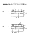
図2及び図3は、本発明の第1実施形態である配線基板1Aを示している。図2は配線基板1Aの部分断面図であり、図3は配線基板1Aを平面視した状態を示している。
配線部材30Aは、ベース体17、第2配線層18a、第3配線層18b、及びソルダーレジスト21,22等により構成されている。ベース体17は配線部材30Aの略中央位置に設けられている。このベース体17は、上部に位置するベース半体17aと、下部に位置するベース半体17bとにより構成されている。
(第2実施形態)
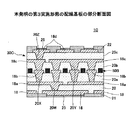
次に、本発明の第2実施形態について説明する。図7は第2実施形態である配線基板1Bを示す断面図であり、図8乃至図10は配線基板1Bの製造方法を示している。尚、図8乃至図10において、第1実施形態の説明に用いた図2乃至図6で示した構成と対応する構成については、同一符号を付してその説明は適宜省略することとする。
(第3実施形態)
次に、本発明の第3実施形態について説明する。図11は第3実施形態である配線基板1Cを示す断面図であり、図12及び図13は配線基板1Cの製造方法を示している。尚、以下説明する各実施形態で用いる図11乃至図17において、第2実施形態の説明に用いた図7乃至図10で示した構成と対応する構成については、同一符号を付してその説明は適宜省略することとする。
(第4実施形態)
次に、本発明の第4実施形態について説明する。図14は第4実施形態である配線基板1Dを示す断面図であり、図15乃至図17は配線基板1Bの製造方法を示している。
10 支持体
13 保護テープ
14 Cu箔
16,28 レジスト材
17 ベース体
18 第1配線層
18a 第2配線層
18b 第3配線層
18c 第4配線層
18d 第5配線層
20 第1絶縁層
20-1,20-2,20c-1,20C-2 絶縁層半体
20a 第2絶縁層
20b 第3絶縁層
20c 第4絶縁層
27 シード層
30A〜30D 配線部材
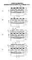
50A〜50E,50-1,50-2 補強体
51A,51B 線状部材
Claims (10)
- 絶縁層と配線層とが積層されてなる配線部材と、
該配線部材の前記絶縁層間に設けられた補強体とを有する配線基板であって、
該補強体は、複数の線状部材を交錯させた構成である配線基板。 - 前記補強体は、前記配線部材の厚さ方向に対する中心位置に配設されてなる請求項1記載の配線基板。
- 前記補強体は、前記配線部材の厚さ方向に対する中心位置を挟んでその上下に離間して配置されてなる請求項1記載の配線基板。
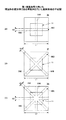
- 前記補強体は、平面視で、少なくとも十字形状、アスタリスク形状、メッシュ形状から選択される一の形状を有してなる請求項1乃至3のいずか一項に記載の配線基板。
- 複数の線状部材を交錯させた構成とされた補強体に保護部材を配設する工程と、
該保護部材上に金属膜により電極を形成する工程と、
該保護部材及び前記補強体を覆うよう第1の樹脂部材を形成することによりベース半体を形成する工程と、
該ベース半体から前記保護部材を除去すると共に、該保護部材が除去された面に第2の樹脂材を配設する工程と、
前記第1及び第2の樹脂部材に、前記電極を露出させる開口部を形成する工程と、
前記開口部内及び前記第1及び第2の樹脂部材の表面に配線金属層を形成することによりベース体を形成する工程と、
該ベース体上に配線層と絶縁層を積層して配線部材を形成する工程と、
を有する配線基板の製造方法。 - 支持体上に配線層と絶縁層を積層して配線部材を形成する工程と、
前記配線部材から前記支持基板を除去する工程とを有する配線基板の製造方法において、
前記配線部材の形成途中に、前記絶縁層上に複数の線状部材を交錯させた構成の補強体を設ける工程を行う配線基板の製造方法。 - 前記補強体を設ける工程は、
前記配線部材の形成途中に複数回実施する請求項6記載の配線基板の製造方法。 - 前記補強体を設ける工程は、
前記配線部材の形成途中において、前記配線部材が所定厚さの半分まで形成された際に1回実施する請求項6記載の配線基板の製造方法。 - 前記補強体を設ける工程では、
前記補強体を前記絶縁層上に搭載する請求項6乃至8のいずれか一項に記載の配線基板の製造方法。 - 前記補強体を設ける工程は、
めっき法を用いて前記絶縁層上に前記補強体を形成する処理を含む請求項6乃至8のいずれか一項に記載の配線基板の製造方法。
Priority Applications (5)
| Application Number | Priority Date | Filing Date | Title |
|---|---|---|---|
| JP2007308583A JP2009135184A (ja) | 2007-11-29 | 2007-11-29 | 配線基板及びその製造方法 |
| TW097144822A TW200924595A (en) | 2007-11-29 | 2008-11-20 | Wiring substrate and manufacturing method thereof |
| US12/323,648 US20090139751A1 (en) | 2007-11-29 | 2008-11-26 | Wiring substrate and manufacturing method thereof |
| KR1020080118746A KR20090056860A (ko) | 2007-11-29 | 2008-11-27 | 배선기판 및 그 제조방법 |
| EP08170158A EP2066157A3 (en) | 2007-11-29 | 2008-11-27 | Wiring substrate and manufacturing method thereof |
Applications Claiming Priority (1)
| Application Number | Priority Date | Filing Date | Title |
|---|---|---|---|
| JP2007308583A JP2009135184A (ja) | 2007-11-29 | 2007-11-29 | 配線基板及びその製造方法 |
Publications (2)
| Publication Number | Publication Date |
|---|---|
| JP2009135184A true JP2009135184A (ja) | 2009-06-18 |
| JP2009135184A5 JP2009135184A5 (ja) | 2010-10-07 |
Family
ID=40410186
Family Applications (1)
| Application Number | Title | Priority Date | Filing Date |
|---|---|---|---|
| JP2007308583A Pending JP2009135184A (ja) | 2007-11-29 | 2007-11-29 | 配線基板及びその製造方法 |
Country Status (5)
| Country | Link |
|---|---|
| US (1) | US20090139751A1 (ja) |
| EP (1) | EP2066157A3 (ja) |
| JP (1) | JP2009135184A (ja) |
| KR (1) | KR20090056860A (ja) |
| TW (1) | TW200924595A (ja) |
Cited By (4)
| Publication number | Priority date | Publication date | Assignee | Title |
|---|---|---|---|---|
| JP2011108959A (ja) * | 2009-11-20 | 2011-06-02 | Kyocera Corp | 配線基板およびプローブカードならびに電子装置 |
| JP2015008214A (ja) * | 2013-06-25 | 2015-01-15 | 株式会社デンソー | 電子装置 |
| US9814137B2 (en) | 2013-10-24 | 2017-11-07 | Murata Manufacturing Co., Ltd. | Wiring board and method of manufacturing same |
| JP2020533805A (ja) * | 2017-09-15 | 2020-11-19 | ステムコ カンパニー リミテッド | 回路基板およびその製造方法 |
Families Citing this family (10)
| Publication number | Priority date | Publication date | Assignee | Title |
|---|---|---|---|---|
| JP4473935B1 (ja) * | 2009-07-06 | 2010-06-02 | 新光電気工業株式会社 | 多層配線基板 |
| KR101088792B1 (ko) * | 2009-11-30 | 2011-12-01 | 엘지이노텍 주식회사 | 인쇄회로기판 및 그 제조방법 |
| JP2013038374A (ja) * | 2011-01-20 | 2013-02-21 | Ibiden Co Ltd | 配線板及びその製造方法 |
| KR20120124319A (ko) * | 2011-05-03 | 2012-11-13 | 엘지이노텍 주식회사 | 인쇄회로기판 및 그의 제조 방법 |
| CN104685978B (zh) * | 2012-09-26 | 2018-04-27 | 日立化成株式会社 | 多层配线板及多层配线板的制造方法 |
| KR101814843B1 (ko) | 2013-02-08 | 2018-01-04 | 엘지이노텍 주식회사 | 인쇄회로기판 및 그의 제조 방법 |
| TWI576025B (zh) * | 2014-10-29 | 2017-03-21 | 矽品精密工業股份有限公司 | 基板結構及其製法 |
| WO2016153644A1 (en) * | 2015-03-20 | 2016-09-29 | 3M Innovative Properties Company | Multilayer substrate for a light emitting semi-conductor device package |
| TWI573231B (zh) * | 2015-07-17 | 2017-03-01 | 矽品精密工業股份有限公司 | 封裝基板及其製法 |
| CN113540029A (zh) | 2020-04-16 | 2021-10-22 | 奥特斯奥地利科技与系统技术有限公司 | 部件承载件以及制造和设计部件承载件的方法 |
Citations (1)
| Publication number | Priority date | Publication date | Assignee | Title |
|---|---|---|---|---|
| JP2003136623A (ja) * | 2001-08-22 | 2003-05-14 | Tdk Corp | モジュール部品、コア基板要素集合体、多層基板、コア基板要素集合体の製造方法、多層基板の製造方法、及びモジュール部品の製造方法 |
Family Cites Families (10)
| Publication number | Priority date | Publication date | Assignee | Title |
|---|---|---|---|---|
| US3277347A (en) * | 1955-10-12 | 1966-10-04 | Minnesota Mining & Mfg | Electric circuit panelboard |
| JPS5831753B2 (ja) * | 1979-02-02 | 1983-07-08 | 鐘淵化学工業株式会社 | 電気用絶縁積層板及び印刷回路用金属箔張り積層板 |
| TW200638811A (en) * | 2004-09-21 | 2006-11-01 | Ibiden Co Ltd | Flexible printed wiring board |
| JP4072176B2 (ja) * | 2005-08-29 | 2008-04-09 | 新光電気工業株式会社 | 多層配線基板の製造方法 |
| JP4452222B2 (ja) * | 2005-09-07 | 2010-04-21 | 新光電気工業株式会社 | 多層配線基板及びその製造方法 |
| JP4377867B2 (ja) * | 2005-09-30 | 2009-12-02 | 日本ピラー工業株式会社 | 銅張積層板、プリント配線板及び多層プリント配線板並びにこれらの製造方法 |
| IL171378A (en) * | 2005-10-11 | 2010-11-30 | Dror Hurwitz | Integrated circuit support structures and the fabrication thereof |
| JP4334005B2 (ja) * | 2005-12-07 | 2009-09-16 | 新光電気工業株式会社 | 配線基板の製造方法及び電子部品実装構造体の製造方法 |
| JP2007227561A (ja) * | 2006-02-22 | 2007-09-06 | Renesas Technology Corp | 半導体装置及びその製造方法 |
| US7737370B2 (en) * | 2006-07-31 | 2010-06-15 | Hitachi Cable, Ltd. | Electromagnetic shielding filter |
-
2007
- 2007-11-29 JP JP2007308583A patent/JP2009135184A/ja active Pending
-
2008
- 2008-11-20 TW TW097144822A patent/TW200924595A/zh unknown
- 2008-11-26 US US12/323,648 patent/US20090139751A1/en not_active Abandoned
- 2008-11-27 EP EP08170158A patent/EP2066157A3/en not_active Withdrawn
- 2008-11-27 KR KR1020080118746A patent/KR20090056860A/ko not_active Application Discontinuation
Patent Citations (1)
| Publication number | Priority date | Publication date | Assignee | Title |
|---|---|---|---|---|
| JP2003136623A (ja) * | 2001-08-22 | 2003-05-14 | Tdk Corp | モジュール部品、コア基板要素集合体、多層基板、コア基板要素集合体の製造方法、多層基板の製造方法、及びモジュール部品の製造方法 |
Cited By (6)
| Publication number | Priority date | Publication date | Assignee | Title |
|---|---|---|---|---|
| JP2011108959A (ja) * | 2009-11-20 | 2011-06-02 | Kyocera Corp | 配線基板およびプローブカードならびに電子装置 |
| JP2015008214A (ja) * | 2013-06-25 | 2015-01-15 | 株式会社デンソー | 電子装置 |
| US9814137B2 (en) | 2013-10-24 | 2017-11-07 | Murata Manufacturing Co., Ltd. | Wiring board and method of manufacturing same |
| JP2020533805A (ja) * | 2017-09-15 | 2020-11-19 | ステムコ カンパニー リミテッド | 回路基板およびその製造方法 |
| US11147160B2 (en) | 2017-09-15 | 2021-10-12 | Stemco Co., Ltd. | Circuit board and method for manufacturing same |
| JP7002643B2 (ja) | 2017-09-15 | 2022-01-20 | ステムコ カンパニー リミテッド | 回路基板およびその製造方法 |
Also Published As
| Publication number | Publication date |
|---|---|
| EP2066157A2 (en) | 2009-06-03 |
| KR20090056860A (ko) | 2009-06-03 |
| EP2066157A3 (en) | 2011-03-09 |
| TW200924595A (en) | 2009-06-01 |
| US20090139751A1 (en) | 2009-06-04 |
Similar Documents
| Publication | Publication Date | Title |
|---|---|---|
| JP2009135184A (ja) | 配線基板及びその製造方法 | |
| KR101751232B1 (ko) | 일체식 구조적 요소를 갖는 다층 전자 구조체의 제조방법 | |
| KR101342031B1 (ko) | 다층 배선 기판 및 그 제조 방법 | |
| JP5144222B2 (ja) | 配線基板及びその製造方法 | |
| KR101329896B1 (ko) | 다층 배선기판 및 그 제조방법 | |
| US8581388B2 (en) | Multilayered wiring substrate | |
| US9763332B2 (en) | Support body, method of manufacturing support body, method of manufacturing wiring board, method of manufacturing electronic component, and wiring structure | |
| JP5096855B2 (ja) | 配線基板の製造方法及び配線基板 | |
| US20110154658A1 (en) | Circuit substrate and manufacturing method thereof | |
| JP4452650B2 (ja) | 配線基板およびその製造方法 | |
| JP2018032657A (ja) | プリント配線板およびプリント配線板の製造方法 | |
| JP2018032660A (ja) | プリント配線板およびプリント配線板の製造方法 | |
| US20090134530A1 (en) | Wiring substrate and method of manufacturing the same | |
| JP6637847B2 (ja) | 配線基板、配線基板の製造方法 | |
| KR101167422B1 (ko) | 캐리어 부재 및 이를 이용한 인쇄회로기판의 제조방법 | |
| JP2623980B2 (ja) | 半導体搭載用リード付き基板の製造法 | |
| JP5269757B2 (ja) | 多層配線基板 | |
| JP4335075B2 (ja) | 多層プリント配線基板およびその製造方法 | |
| JP2004087886A (ja) | 多層配線板の製造方法及び多層配線板 | |
| JP2004259776A (ja) | 回路基板とその製造方法 | |
| JPH09172122A (ja) | 半導体搭載用リ−ド付き基板の製造法 | |
| KR20100116931A (ko) | 인쇄회로기판 및 그 제조방법 | |
| JP2009206229A (ja) | 半導体装置およびその製造方法 |
Legal Events
| Date | Code | Title | Description |
|---|---|---|---|
| A521 | Request for written amendment filed |
Free format text: JAPANESE INTERMEDIATE CODE: A523 Effective date: 20100823 |
|
| A621 | Written request for application examination |
Free format text: JAPANESE INTERMEDIATE CODE: A621 Effective date: 20100823 |
|
| A977 | Report on retrieval |
Free format text: JAPANESE INTERMEDIATE CODE: A971007 Effective date: 20120119 |
|
| A131 | Notification of reasons for refusal |
Free format text: JAPANESE INTERMEDIATE CODE: A131 Effective date: 20120124 |
|
| A02 | Decision of refusal |
Free format text: JAPANESE INTERMEDIATE CODE: A02 Effective date: 20120529 |