JP2009054503A - Display device and its light emitting method - Google Patents
Display device and its light emitting method Download PDFInfo
- Publication number
- JP2009054503A JP2009054503A JP2007221980A JP2007221980A JP2009054503A JP 2009054503 A JP2009054503 A JP 2009054503A JP 2007221980 A JP2007221980 A JP 2007221980A JP 2007221980 A JP2007221980 A JP 2007221980A JP 2009054503 A JP2009054503 A JP 2009054503A
- Authority
- JP
- Japan
- Prior art keywords
- light
- display device
- image display
- optical filter
- light emitting
- Prior art date
- Legal status (The legal status is an assumption and is not a legal conclusion. Google has not performed a legal analysis and makes no representation as to the accuracy of the status listed.)
- Withdrawn
Links
- 238000000034 method Methods 0.000 title claims abstract description 50
- 239000000758 substrate Substances 0.000 claims abstract description 42
- 230000003287 optical effect Effects 0.000 claims abstract description 22
- 239000000463 material Substances 0.000 claims description 12
- 238000007789 sealing Methods 0.000 abstract description 25
- 238000000605 extraction Methods 0.000 abstract description 9
- 239000011521 glass Substances 0.000 description 18
- 238000005401 electroluminescence Methods 0.000 description 17
- 239000011159 matrix material Substances 0.000 description 15
- 239000010408 film Substances 0.000 description 14
- 230000006870 function Effects 0.000 description 9
- 238000010586 diagram Methods 0.000 description 8
- 238000002347 injection Methods 0.000 description 8
- 239000007924 injection Substances 0.000 description 8
- 239000002184 metal Substances 0.000 description 8
- 239000002904 solvent Substances 0.000 description 7
- 239000011248 coating agent Substances 0.000 description 5
- 238000000576 coating method Methods 0.000 description 5
- 230000000694 effects Effects 0.000 description 5
- 239000011368 organic material Substances 0.000 description 5
- 230000009471 action Effects 0.000 description 4
- YXFVVABEGXRONW-UHFFFAOYSA-N Toluene Chemical compound CC1=CC=CC=C1 YXFVVABEGXRONW-UHFFFAOYSA-N 0.000 description 3
- 230000006399 behavior Effects 0.000 description 3
- 238000004519 manufacturing process Methods 0.000 description 3
- 230000010287 polarization Effects 0.000 description 3
- 230000008569 process Effects 0.000 description 3
- 238000005070 sampling Methods 0.000 description 3
- 239000004642 Polyimide Substances 0.000 description 2
- 238000010521 absorption reaction Methods 0.000 description 2
- 230000000903 blocking effect Effects 0.000 description 2
- 239000003990 capacitor Substances 0.000 description 2
- 239000003086 colorant Substances 0.000 description 2
- 230000007423 decrease Effects 0.000 description 2
- 238000005274 electrospray deposition Methods 0.000 description 2
- 238000003475 lamination Methods 0.000 description 2
- 230000031700 light absorption Effects 0.000 description 2
- 238000000206 photolithography Methods 0.000 description 2
- 229920001721 polyimide Polymers 0.000 description 2
- 238000004544 sputter deposition Methods 0.000 description 2
- 238000007740 vapor deposition Methods 0.000 description 2
- 230000002411 adverse Effects 0.000 description 1
- 239000007864 aqueous solution Substances 0.000 description 1
- 230000008033 biological extinction Effects 0.000 description 1
- 230000005540 biological transmission Effects 0.000 description 1
- 238000004364 calculation method Methods 0.000 description 1
- 238000009125 cardiac resynchronization therapy Methods 0.000 description 1
- 230000008859 change Effects 0.000 description 1
- 238000006243 chemical reaction Methods 0.000 description 1
- 238000005229 chemical vapour deposition Methods 0.000 description 1
- 238000013500 data storage Methods 0.000 description 1
- 230000006866 deterioration Effects 0.000 description 1
- 238000011161 development Methods 0.000 description 1
- 238000009826 distribution Methods 0.000 description 1
- 238000005265 energy consumption Methods 0.000 description 1
- 239000004973 liquid crystal related substance Substances 0.000 description 1
- 239000000203 mixture Substances 0.000 description 1
- 239000003960 organic solvent Substances 0.000 description 1
- 239000004033 plastic Substances 0.000 description 1
- 229920000642 polymer Polymers 0.000 description 1
- 239000002861 polymer material Substances 0.000 description 1
- 230000002250 progressing effect Effects 0.000 description 1
- 230000036632 reaction speed Effects 0.000 description 1
- 238000012827 research and development Methods 0.000 description 1
- 239000013557 residual solvent Substances 0.000 description 1
- 238000004528 spin coating Methods 0.000 description 1
- 239000007921 spray Substances 0.000 description 1
- 239000010409 thin film Substances 0.000 description 1
- 230000032258 transport Effects 0.000 description 1
- 238000001771 vacuum deposition Methods 0.000 description 1
Images


Classifications
-
- H—ELECTRICITY
- H10—SEMICONDUCTOR DEVICES; ELECTRIC SOLID-STATE DEVICES NOT OTHERWISE PROVIDED FOR
- H10K—ORGANIC ELECTRIC SOLID-STATE DEVICES
- H10K59/00—Integrated devices, or assemblies of multiple devices, comprising at least one organic light-emitting element covered by group H10K50/00
- H10K59/80—Constructional details
- H10K59/875—Arrangements for extracting light from the devices
-
- H—ELECTRICITY
- H10—SEMICONDUCTOR DEVICES; ELECTRIC SOLID-STATE DEVICES NOT OTHERWISE PROVIDED FOR
- H10K—ORGANIC ELECTRIC SOLID-STATE DEVICES
- H10K50/00—Organic light-emitting devices
- H10K50/80—Constructional details
- H10K50/85—Arrangements for extracting light from the devices
-
- H—ELECTRICITY
- H10—SEMICONDUCTOR DEVICES; ELECTRIC SOLID-STATE DEVICES NOT OTHERWISE PROVIDED FOR
- H10K—ORGANIC ELECTRIC SOLID-STATE DEVICES
- H10K50/00—Organic light-emitting devices
- H10K50/80—Constructional details
- H10K50/84—Passivation; Containers; Encapsulations
- H10K50/844—Encapsulations
-
- H—ELECTRICITY
- H10—SEMICONDUCTOR DEVICES; ELECTRIC SOLID-STATE DEVICES NOT OTHERWISE PROVIDED FOR
- H10K—ORGANIC ELECTRIC SOLID-STATE DEVICES
- H10K50/00—Organic light-emitting devices
- H10K50/80—Constructional details
- H10K50/86—Arrangements for improving contrast, e.g. preventing reflection of ambient light
-
- H—ELECTRICITY
- H10—SEMICONDUCTOR DEVICES; ELECTRIC SOLID-STATE DEVICES NOT OTHERWISE PROVIDED FOR
- H10K—ORGANIC ELECTRIC SOLID-STATE DEVICES
- H10K59/00—Integrated devices, or assemblies of multiple devices, comprising at least one organic light-emitting element covered by group H10K50/00
- H10K59/80—Constructional details
- H10K59/8791—Arrangements for improving contrast, e.g. preventing reflection of ambient light
Abstract
Description
本発明は、表示装置及びその発光方法に関するものであり、特に、発光した光の干渉効果を抑制するための光学フィルターを備えた表示装置及びその発光方法に関するものである。 The present invention relates to a display device and a light emitting method thereof, and more particularly to a display device including an optical filter for suppressing an interference effect of emitted light and a light emitting method thereof.
電子銃によって電子をスクリーン上の蛍光体に衝突させ、そのエネルギーで蛍光体を発光させるブラウン管(CRT:Cathode Ray Tube)は、表示品質とコストの点で秀でており、長い間、テレビやパソコンなどの表示装置として使用されてきた。 CRT (Cathode Ray Tube), which uses an electron gun to collide electrons with phosphors on the screen and emits phosphors with the energy, has been excellent in terms of display quality and cost. It has been used as a display device.
近年では、重くて嵩高いCRTから、省スペースの利便性、携帯性を重視するフラットパネルディスプレイ(FPD:Flat Panel Display)の研究開発が進み、製品化もなされている。FPDには、非発光型の液晶ディスプレイや、自発光型のプラズマディスプレイ(PD)、フィールドエミッションディスプレイ(FED)、有機EL(Electro Luminescence)ディスプレイなどがある。 In recent years, research and development of flat panel displays (FPDs) that emphasize the convenience of space saving and portability have progressed from the heavy and bulky CRTs, and commercialization has also been made. The FPD includes a non-light emitting liquid crystal display, a self-light emitting plasma display (PD), a field emission display (FED), an organic EL (Electro Luminescence) display, and the like.
これらの表示装置には、室内灯や、部屋に差し込んでくる太陽光などの外光による画質劣化を防ぐために、表示装置表面に円偏光フィルターを設けたものがある。 Some of these display devices are provided with a circularly polarizing filter on the surface of the display device in order to prevent deterioration of image quality due to outside light such as room light or sunlight entering the room.
このような表示装置として、有機ELディスプレイの前面に円偏光フィルターを設けることにより、外光を除去するものが開示されている(特許文献1参照)。 As such a display device, a device that removes external light by disposing a circularly polarizing filter on the front surface of an organic EL display is disclosed (see Patent Document 1).
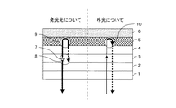
ところで、有機ELディスプレイの大画面化に向けて、高分子材料を用いた塗布型のディスプレイの開発が進んでいる。図6は、塗布型の有機ELディスプレイにおける一般的な画像表示素子の構成を示す模式図である。 By the way, development of a coating-type display using a polymer material is progressing toward the enlargement of the screen of the organic EL display. FIG. 6 is a schematic diagram showing a configuration of a general image display element in a coating type organic EL display.
図6において、画像表示素子は、ガラス基板23、透明電極24、発光に関与する積層25、金属電極26、及び封止層27からなり、さらに、光学フィルター22がガラス基板23の表面に設けられている。光学フィルター22の種類としては、例えば、円偏光フィルターを挙げることができる。
In FIG. 6, the image display element includes a
このような構成からなる画像表示素子について、発光に関与する積層25内で発光した光と、画像表示素子の外部から入射する外光とが、各々どのような振る舞いをするかを説明する。
With respect to the image display element having such a configuration, how the light emitted from the laminated
まず、発光に関与する積層25内で発光した光について説明する。図6(左側)において、符号28で示す星印を1つの発光点とする。有機EL画像表示素子からの発光は、ランダムに配置・配向された双極子からの自然放出光として取り扱うことができ、あらゆる方向に等しい強度で発光している点光源の集まりと考えられる。その点光源は、発光に関与する積層25内で電子とホールのキャリアバランスにより決定される、ある面近傍に多数並んでいる。
First, the light emitted in the
自然放出光の可干渉距離については、異なる点光源同士の発光は干渉しないと考えられる。したがって、1つの点光源から発光した光の干渉だけを考えればよく、その可干渉距離は、波長と同程度か数十波長程度、つまり、数μmである。そこで、発光点28を発光面の代表として、その干渉の影響を考える。
Regarding the coherence distance of spontaneously emitted light, it is considered that light emitted from different point light sources does not interfere. Therefore, it is only necessary to consider interference of light emitted from one point light source, and the coherence distance is about the same as the wavelength or about several tens of wavelengths, that is, several μm. Thus, the influence of the interference is considered with the
発光点28から全方位に発光した光のうち、吸収や、全反射の影響で除去される光を除くと、外部に取り出される光は、次の2つの光束である。すなわち、発光点28からそのままガラス基板23側に出ていく光と、発光点28から、金属電極26側に向かい、金属電極26の表面で反射され、ガラス基板23側に向かう光である。
Excepting light that is emitted in all directions from the
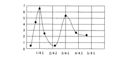
この両者の光は、図6中、符号29で示す点、すなわち発光に関与する積層25と透明電極24の界面等で干渉する。図7は、その干渉により外部に取り出される光の相対的な光量を計算により求めた一例を示している。図7において、横軸は、発光点28から金属電極26の表面までの光学距離で、発光に関与する積層25内での発光波長λを用いて示している。ここで、真空中の発光波長をλ0とし、屈折率nの発光に関与する積層25内での発光波長をλとすると、λ0=n・λとなる。また、図7において、縦軸は相対的な光量である。
These two lights interfere with each other at a point indicated by
図7に示すように、発光点28から金属電極26の表面までの光学距離が1/4λの時に、両者の光が強めあうことがわかり、RGBの三原色の波長に従って、最適な厚みとなるように各画像表示素子の厚みが設計されている。
As shown in FIG. 7, it can be seen that when the optical distance from the
一方、図6(右側)を参照して、外光の振る舞いを説明する。外部から入射した光は円偏光フィルター22を経て、各層を透過し、金属電極26の表面で反射され、再び各層を透過し、円偏光フィルター22を経て、外部に出てくる。この時、円偏光フィルター22と、反射層として機能する金属電極26との働きにより、ほとんどの外光は反射されない。図8を参照して、その働きを説明する。
On the other hand, the behavior of external light will be described with reference to FIG. 6 (right side). Light incident from the outside passes through each layer through the circular polarizing
図8において、円偏光フィルターは、偏光子32と、1/4波長板33とにより構成される。また、図8において、34は反射層であり、図6では、金属電極26の表面がこの反射層として機能する。無偏光の外光35が、x軸方向に直線偏光の透過軸方向を持つ偏光子32を通過すると、x軸方向に沿った直線偏光の光36となる。さらに、直線偏光の光36が、x軸とy軸の45度方向に合わせた1/4波長板33を通過すると、円偏光の光37に変換される。
In FIG. 8, the circularly polarizing filter includes a
円偏光の光37は、反射層34で、反対回りの円偏光の光38として反射される。説明のため、反射光を図8の右側に示す。反射された円偏光の光38は、再び、1/4波長板33を通過することで、直線偏光の光36とは直交する方向に、直線偏光の偏光方向を持つ光39に変換される。偏光子32は、y軸方向の直線偏光の光を吸収するものであるから、直線偏光の光39は、偏光子32により吸収され、外部に反射される光40は偏光子32の消光比に従って減少させられる。
The circularly polarized
このように、光学フィルターとしての円偏光フィルターと反射層との働きにより、外光はほとんど除去される。しかしながら、円偏光フィルターの偏光子32の影響で、発光に関与する積層で発光した光もおよそ半分の光量が吸収されてしまうという問題があった。
Thus, the external light is almost removed by the action of the circular polarizing filter as the optical filter and the reflective layer. However, due to the influence of the
また、他の先行技術として、光取り出し電極とは反対側の透明電極の外側に、光吸収層を配置する技術(特許文献2参照)、あるいは干渉によって反射を防ぐ層を配置する技術(特許文献3参照)が開示されている。 In addition, as another prior art, a technique of disposing a light absorption layer outside the transparent electrode opposite to the light extraction electrode (see Patent Document 2), or a technique of disposing a layer that prevents reflection by interference (Patent Document) 3) is disclosed.
有機ELディスプレイの画像表示素子を設計する際には、図7で示す干渉効果の最適値で膜厚を設計する。しかし、図7から明らかなように、最適値から厚みがずれて画像表示素子が作成されると、急激に外部に取り出される光量が落ちるという問題があった。特に、塗布型で大画面の画像表示素子を作成した場合には、厚み誤差が生じやすく、画面の場所によって、干渉による取り出し光量が変化するという問題があった。 When designing an image display element of an organic EL display, the film thickness is designed with the optimum value of the interference effect shown in FIG. However, as apparent from FIG. 7, when the image display element is created with the thickness deviated from the optimum value, there is a problem that the amount of light taken out suddenly decreases. In particular, when a coating-type large-screen image display element is produced, there is a problem that a thickness error is likely to occur, and the amount of light extracted due to interference varies depending on the location of the screen.
本発明は、上述した事情に鑑み提案されたもので、画像表示素子の膜厚誤差が生じた場合であっても、光の取り出し効率を減少させることがない表示装置及びその発光方法を提供することを目的とする。 The present invention has been proposed in view of the above-described circumstances, and provides a display device and a light emitting method thereof that do not reduce the light extraction efficiency even when a film thickness error of an image display element occurs. For the purpose.
本発明の表示装置及びその発光方法は、上述した目的を達成するため、以下の特徴点を備えている。すなわち、本発明の表示装置は、複数の画像表示素子からなる。そして、各画像表示素子は、少なくとも、発光に関与する複数の層からなる積層と、該積層を間に挟む形で配置された一対の電極と、一方の電極側に配置された透明基板と、他方の電極側に、電極側から順に光学フィルター、反射層が形成されている光学フィルター及び反射層とを含むことを特徴とするものである。 In order to achieve the above-described object, the display device and the light emitting method of the present invention have the following features. That is, the display device of the present invention includes a plurality of image display elements. Each image display element includes at least a laminate composed of a plurality of layers involved in light emission, a pair of electrodes arranged so as to sandwich the laminate, and a transparent substrate arranged on one electrode side, The other electrode side includes an optical filter, an optical filter in which a reflective layer is formed, and a reflective layer in order from the electrode side.
また、本発明の表示装置の発光方法は、発光に関与する複数の層からなる積層内で発光した光のうち、光学フィルター及び反射層を経て透明基板側に向かう光を除去する。また、発光に関与する複数の層からなる積層内で発光した光のうち、そのまま透明基板側に向かう光を透明基板の外側に導くことを特徴とするものである。 In addition, the light emitting method of the display device of the present invention removes light that travels to the transparent substrate side through the optical filter and the reflective layer, from the light emitted in the stack composed of a plurality of layers involved in light emission. In addition, among the light emitted in the stack composed of a plurality of layers involved in light emission, the light directed toward the transparent substrate is directly guided to the outside of the transparent substrate.
本発明の表示装置及びその発光方法によれば、画像表示素子の製造時に膜厚が変動したとしても、急激に光の取り出し効率が変化することがなく、光の取り出し効率を減少させることがない表示装置とすることができる。 According to the display device and the light emitting method of the present invention, even if the film thickness varies during the manufacture of the image display element, the light extraction efficiency does not change abruptly, and the light extraction efficiency does not decrease. It can be a display device.
以下、図面を参照して、本発明の表示装置及びその発光方法を実施するための最良の形態について詳細に説明する。 The best mode for carrying out the display device and the light emitting method thereof according to the present invention will be described below in detail with reference to the drawings.
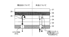
図1は、本発明の実施形態に係る表示装置及びその発光方法に用いる画像表示素子の構成を示す模式図である。 FIG. 1 is a schematic diagram showing a configuration of an image display element used in a display device and a light emitting method thereof according to an embodiment of the present invention.
図1において、1はガラスやプラスチックからなる透明基板で、本実施形態ではガラス基板を用いた。また、2はITOやZnO等からなる第1の透明電極、3は少なくとも1層が有機EL材料からなり、発光に関与する積層である。具体的には、積層3はPEDOT‐PSS等からなるホール注入層、高分子や中分子の塗布可能な有機EL材料からなる発光層、及びCs2CO3等からなる電子注入層などから構成される。もちろん、有機EL発光材料からなる発光層を含む発光に関与する積層3は、これに限定されるものではない。
In FIG. 1,
また、4はITOやZnO等からなる第2の透明電極であり、第1の透明電極2とで一対の電極を構成する。第2の透明電極は、第1の透明電極2と同じ材質であってもよく、あるいは違う材質であってもよい。また、5は光学フィルターとして機能する円偏光フィルターであり、6は反射層として機能する封止層である。ここでは、光学フィルターとして、円偏光フィルター5を例にとって説明するが、その他の機能を兼ね備えたフィルターであってもよい。
図1(左側)において、発光に寄与する積層3内に発光点7が存在するとする。発光点7から全方位に発光した光のうち、吸収や、全反射の影響で除去される光を除くと、次の2つの光束が残る。すなわち、発光点7からそのまま一方の電極である第1の透明電極2側に配置されたガラス基板1側(透明基板側)に出ていく光である。そして、発光点7から、他方の電極である第2の透明電極4側に配置され、反射層として機能する封止層6側に向かい、封止層6の表面で反射され、ガラス基板1側に向かう光である。
In FIG. 1 (left side), it is assumed that a
両者の光が、従来の画像表示素子と同様に存在すると、発光に関与する積層3と第1の透明電極2の界面8等で干渉する。
When both lights exist in the same manner as in a conventional image display element, they interfere with each other at the
しかしながら、本実施形態の発光装置及びその発光方法では、発光点7と、反射層として機能する封止層6の間に、円偏光フィルター5が配置されている。したがって、発光点7から封止層6側(すなわち、光学フィルター及び反射層側)に向かう光は、円偏光フィルター5と封止層6との働きによって、封止層6の表面で反射される。そして、円偏光フィルター5を出る段階(図中、符号9で示すポイント)で除去されることになる。これは、図8で示す外光の振る舞いと同様である。すなわち、発光点7から、反射層として機能する封止層6側に向かった光は干渉ポイント8に戻ってこないため、発光点7からそのままガラス基板1側に出ていく光との干渉現象が生じない。
However, in the light emitting device and the light emitting method of the present embodiment, the circularly
ここで、発光層では等方的に発光しているので、発光点7から反射層として機能する封止層6側に向かった光と、発光点7からそのままガラス基板1側に出ていく光はほぼ同等の光量と考えられる。本実施形態のように、発光点7から、反射層として機能する封止層6側に向かった光だけを除去したとすると、50%の光が除去されたことになる。これは、ガラス基板の表面に円偏光フィルターを配置した従来例において、円偏光フィルターにより、外に向かう光の50%の光量を除去するものと同等になっている。
Here, since the light emitting layer emits isotropically, the light traveling from the
しかしながら、本実施形態では、膜厚誤差による、取り出し効率の急激なムラを解消することができるので、画像表示素子作成の容易さを向上することができる。 However, according to the present embodiment, it is possible to eliminate a sudden unevenness in the extraction efficiency due to a film thickness error, and therefore it is possible to improve the ease of creating an image display element.
次に、図1(右側)を参照して、外光の振る舞いを説明する。図1に示すように、外部から入射した光のほとんどは、ガラス基板1、第1の透明電極2、発光に寄与する積層3、第2の透明電極4を透過して、円偏光フィルター5に入射し、反射層として機能する封止層6で反射され、再び、円偏光フィルター5に入る。ここで、円偏光フィルター5と反射層として機能する封止層6との働きは、図8で示したものと同様である。したがって、符号10で示すポイントにおいて、外光は円偏光フィルター5を出たところで除去されることになり、再び、ガラス基板1を出て外に放射されることはない。
Next, the behavior of outside light will be described with reference to FIG. As shown in FIG. 1, most of the light incident from the outside passes through the
このように、発光点7と反射層として機能する封止層6との間に円偏光フィルター5を配置しても、従来の画像表示素子と同様に外光を除去することができる。
As described above, even when the circularly
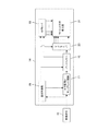
次に、図2を参照して、本発明の実施形態に係る表示装置に用いる画像表示素子の作成手順を説明する。図2は、本発明の実施形態に係る表示装置に用いる画像表示素子の作成手順を示すフローチャートである。 Next, with reference to FIG. 2, a procedure for creating an image display element used in the display device according to the embodiment of the present invention will be described. FIG. 2 is a flowchart showing a procedure for creating an image display element used in the display device according to the embodiment of the present invention.
本発明の実施形態に係る表示装置に用いる画像表示素子を作成するには、図2に示すように、まず、製造装置に基板となるガラス基板を投入し、駆動方法に応じて配線等を作成する(S1)。具体的には、アクティブマトリックス駆動の場合に、スイッチングや駆動電流を流すためのTFTとデータ記憶用のキャパシターなどを作成する。 In order to create an image display element used in a display device according to an embodiment of the present invention, as shown in FIG. 2, first, a glass substrate as a substrate is put into a manufacturing apparatus, and wirings and the like are created according to the driving method. (S1). Specifically, in the case of active matrix driving, a TFT for passing switching and driving current, a capacitor for storing data, and the like are created.
続いて、駆動方法に応じて処置が施されたガラス基板に対して、スパッタ蒸着やフォトリソグラフの工程を経て、表示画素の配置に応じて、ITO等の第1の透明電極を形成する(S2)。 Subsequently, a first transparent electrode such as ITO is formed on the glass substrate treated according to the driving method, through sputter deposition and photolithography processes, depending on the arrangement of display pixels (S2). ).
次に、発光に寄与する積層を順次形成する。ここで、低分子の有機EL材料を用いる場合には、蒸着によって積層を形成する。この方法は、膜厚を制御し易いが、大画面を製造するのが困難であるという特徴がある。また、中分子または高分子の有機EL材料を用いる場合には、塗布によって積層を形成することができ、大画面の表示装置の製造が可能となる。本実施形態では、塗布によって積層を形成する方法を説明する。 Next, a stack that contributes to light emission is sequentially formed. Here, when a low-molecular organic EL material is used, a stacked layer is formed by vapor deposition. This method is characterized in that it is easy to control the film thickness, but it is difficult to produce a large screen. Further, in the case of using a medium molecular or high molecular organic EL material, a laminate can be formed by coating, and a large-screen display device can be manufactured. In this embodiment, a method for forming a stack by coating will be described.
塗布によって積層を形成する方法には、数種類ある。例えば、圧電素子等によりノズルに圧力を加え、溶媒に溶かした有機材料等を基板に噴射するインクジェット方式がある。また、基板に溝(バンク)を形成し、細いノズルを用いて、溶媒に溶かした有機材料等を溝の間に流しこむノズル方式がある。また、溶媒に溶かした有機材料等を霧状にして基盤に噴霧するスプレーCVD方式がある。また、ノズルと基板間に電圧をかけて、積極的に溶媒に溶かした有機材料等を基板に噴射するESD(Electro Spray Deposition)方式がある。本実施形態では、ノズル方式を用いて積層を形成するが、他の方式であっても本発明に適応できることは勿論である。 There are several methods for forming a stack by coating. For example, there is an ink jet system in which pressure is applied to a nozzle by a piezoelectric element or the like, and an organic material or the like dissolved in a solvent is jetted onto a substrate. In addition, there is a nozzle system in which grooves (banks) are formed in a substrate and an organic material or the like dissolved in a solvent is poured between the grooves using a thin nozzle. Further, there is a spray CVD method in which an organic material or the like dissolved in a solvent is atomized and sprayed on a substrate. Further, there is an ESD (Electro Spray Deposition) method in which a voltage is applied between the nozzle and the substrate, and an organic material or the like that is actively dissolved in a solvent is sprayed onto the substrate. In this embodiment, the lamination is formed using the nozzle method, but it is needless to say that other methods can be applied to the present invention.
上述したステップ2(S2)に続いて、基板上に、溶媒に溶かした有機材料等を塗布するために必要なバンクを形成する(S3)。バンクの材料として、ポリイミドなどを用いることができる。ポリイミドを溶媒に溶かし、スピンコート法等により基板全体に塗布し、フォトリソグラフ工程で表示画素に応じたバンクが形成される。その後、バンクを硬化するためにベークを行う。 Subsequent to step 2 (S2) described above, a bank necessary for applying an organic material or the like dissolved in a solvent is formed on the substrate (S3). Polyimide or the like can be used as the bank material. A polyimide is dissolved in a solvent and applied to the entire substrate by a spin coating method or the like, and a bank corresponding to the display pixel is formed in a photolithography process. Thereafter, baking is performed to cure the bank.
次に、発光に寄与する積層を形成する。 Next, a stack that contributes to light emission is formed.
発光に寄与する積層を形成する工程では、まず、基板上にホール注入層を形成する(S4)。具体的には、PEDOT−PSSをホール注入層とした場合を考えると、ノズル方式により、PEDOT−PSSの水溶液をバンク間に流し込みホール注入層を形成する。その後、残留溶媒を飛ばすために、ベークを行う。 In the step of forming a stack that contributes to light emission, first, a hole injection layer is formed on a substrate (S4). Specifically, considering the case where PEDOT-PSS is used as a hole injection layer, an aqueous solution of PEDOT-PSS is poured between banks by a nozzle method to form a hole injection layer. Thereafter, baking is performed to remove residual solvent.
続いて、RGBの3原色に応じた有機EL材料をトルエン等の有機溶剤に溶かし、それぞれ別のノズルを用いてホール注入層の上でバンク間に流し込み、発光層を形成する(S5)。従来の画像表示素子では、干渉の効果を用いていたので、各色別々に最適な膜厚があり、大画面の基板全面で、膜厚を均一にするのはとても困難であった。これに対して、本実施形態では、光の干渉の効果は少なく、膜厚に対する要求は減じられている。 Subsequently, an organic EL material corresponding to the three primary colors of RGB is dissolved in an organic solvent such as toluene, and is poured between the banks on the hole injection layer using different nozzles to form a light emitting layer (S5). Since the conventional image display element uses the effect of interference, there is an optimum film thickness for each color, and it has been very difficult to make the film thickness uniform over the entire surface of a large-screen substrate. On the other hand, in this embodiment, the effect of light interference is small, and the demand for film thickness is reduced.
続いて、電子注入層を形成する(S6)。具体的には、真空蒸着等により、発光層の上にCs2CO3からなる電子注入層を形成する。 Subsequently, an electron injection layer is formed (S6). Specifically, an electron injection layer made of Cs 2 CO 3 is formed on the light emitting layer by vacuum deposition or the like.
続いて、第2の透明電極として、スパッタ蒸着等によりITOを形成する(S7)。 Subsequently, ITO is formed as the second transparent electrode by sputtering vapor deposition or the like (S7).
続いて、円偏光フィルターを形成する(S8)。ここでは、円偏光フィルターとして、フィルム状に作成されたものを用いて、基板全体を覆う形で作成する。 Subsequently, a circularly polarizing filter is formed (S8). Here, the circular polarizing filter is prepared in a form that covers the entire substrate using a film-shaped filter.
最後に、封止処理を行う(S9)。この際、CVD等で封止膜を形成してもよいし、ステップ7(S7)において、予めフィルム状の円偏光フィルターの裏面に封止膜を形成しておき、透明電極上に封止膜付きの円偏光フィルターを覆うように形成してもよい。すなわち、円偏光フィルター及び反射層をフィルム状に形成しておき、画像表示素子の片面を覆うことで画像表示素子を封止することもできる。 Finally, a sealing process is performed (S9). At this time, a sealing film may be formed by CVD or the like. In step 7 (S7), a sealing film is previously formed on the back surface of the film-like circularly polarizing filter, and the sealing film is formed on the transparent electrode. It may be formed so as to cover the attached circularly polarizing filter. That is, the image display element can be sealed by forming the circularly polarizing filter and the reflective layer in a film shape and covering one side of the image display element.
以上の工程で、本発明の実施形態に係る表示装置に用いる画像表示素子が作成される。なお、発光に寄与する積層を作成する工程で、キャリア分布を調整するための電子ブロッキング層やホールブロッキング層を形成しもよいし、ノズル方式により、ホールを発光層に輸送する層を形成してもよい。また、これらの層を形成する際に、光で硬化する性質の材料を用いて、各層上に塗布する溶剤に材料が溶けないようにしてもよい。 Through the above steps, an image display element used in the display device according to the embodiment of the present invention is created. In the step of creating a layer that contributes to light emission, an electron blocking layer or a hole blocking layer for adjusting carrier distribution may be formed, or a layer that transports holes to the light emitting layer is formed by a nozzle method. Also good. Further, when these layers are formed, a material having a property of being cured by light may be used so that the material does not dissolve in a solvent applied on each layer.
次に、本発明の表示装置及びその発光方法の他の実施形態を説明する。 Next, other embodiments of the display device and the light emitting method thereof according to the present invention will be described.
図3及び図4は、本発明の他の実施形態に係る表示装置及びその発光方法に用いる画像表示素子の構成を示す模式図である。なお、上述した実施形態と同様の機能を有する部分には同一の符号を付して、詳細な説明を省略する。 3 and 4 are schematic views showing the configuration of a display device according to another embodiment of the present invention and an image display element used in the light emitting method. In addition, the same code | symbol is attached | subjected to the part which has the function similar to embodiment mentioned above, and detailed description is abbreviate | omitted.
図3に示す画像表示素子は、円偏光フィルター5と封止層12との間に積極的に反射層11を形成し、その上に封止層12を形成したものである。このような構成とすることにより、反射層として機能する封止層12において一部の光が透過して迷光となり、他の色の画像表示素子や、TFT等に有害な影響を及ぼさないようにすることができる。
In the image display element shown in FIG. 3, the
図4に示す画像表示素子は、ガラス基板1の表面で反射される外光の影響を除くために、ガラス基板1の下に外光の拡散反射層13を形成したものである。このような構成とすることにより、表示装置を見ている人の像や、室内灯などの映り込みを除外することができる。
In the image display element shown in FIG. 4, a diffuse reflection layer 13 for external light is formed under the
次に、上述した画像表示素子を用いた表示装置について説明する。 Next, a display device using the above-described image display element will be described.
図5は、本発明の実施形態に係る表示装置を示すブロック図である。 FIG. 5 is a block diagram showing the display device according to the embodiment of the present invention.
本発明の実施形態に係る表示装置14は、上述した画像表示素子を用いて構成されている。この表示装置14は、図5に示すように、少なくとも、表示制御部16、A/D変換orサンプリング回路17、バッファメモリ18、Xドライバ19、Yドライバ20、及びマトリックス型の表示部21を有している。
The
表示制御部16は、外部から入力される映像信号15を各画素のデジタルデータに変換し、マトリックス型の表示部21に表示する一連の操作を制御するためのものである。
The
表示装置14に入力される映像信号15は、ビデオ信号等のアナログ信号であってもよいし、DVD等のデジタル信号であってもよい。映像信号15が表示装置14に入力されると、表示制御部16の制御に従って、A/D変換orサンプリング回路17において各画素の表示データに変換される。そして、各画素の表示データは、バッファメモリ18に格納される。
The
一方、バッファメモリ18に格納されている各画素の表示データは、表示制御部16の制御に従って読み出される。そして、Xドライバ19及びYドライバ20により、表示部21に対応した各画像表示素子に対して表示データを書き込むことで、画像が表示される。
On the other hand, the display data of each pixel stored in the
表示部21は、画像表示素子がマトリックス状に並んで構成される。画像表示素子の駆動方式を大別すると、パッシブマトリックス駆動方式と、アクティブマトリックス駆動方式とがある。
The
パッシブマトリックス駆動方式は構造がシンプルであり、列と行に分けた信号電極と、走査電極の交点の電極との間に電圧を与え、両電極間に挟まれた画素を光らせる駆動方式である。このパッシブマトリックス駆動方式は、小画面の有機ELディスプレイに採用されている。一方、アクティブマトリックス駆動方式は、画素毎に数個のTFT(Thin Film Transistor)と、データ記憶用のキャパシターとを必要とする。しかし、アクティブマトリックス駆動方式は、パッシブマトリックス駆動方式に比べて反応速度が短く、また、大画面にすると、駆動電圧やエネルギー消費の点で優位になる。したがって、このアクティブマトリックス駆動方式は、大画面の有機ELディスプレイに採用されている。 The passive matrix driving method has a simple structure and is a driving method in which a voltage is applied between the signal electrode divided into columns and rows and the electrode at the intersection of the scanning electrodes, and the pixels sandwiched between the two electrodes are illuminated. This passive matrix driving method is employed in small screen organic EL displays. On the other hand, the active matrix driving method requires several TFTs (Thin Film Transistors) and a capacitor for data storage for each pixel. However, the active matrix driving method has a shorter reaction speed than the passive matrix driving method, and a large screen is advantageous in terms of driving voltage and energy consumption. Therefore, this active matrix driving method is employed in a large screen organic EL display.
本実施形態では、アクティブマトリックス駆動方式を用いた大画面の有機ELディスプレイとしているが、小型の画面で用いられているパッシブマトリックス駆動であっても、本発明を適応することができる。 In this embodiment, an organic EL display having a large screen using an active matrix driving method is used. However, the present invention can be applied even to passive matrix driving used in a small screen.
以上説明したように、本発明の表示装置は、複数の画像表示素子からなる表示装置において、発光に関与する積層内の発光点と、反射層として機能する封止層との間に円偏光フィルターを配置した構成となっている。このような構成とすることにより、画像表示素子の製造時において膜厚が変動したとしても、光取り出し量の変動を抑制することができる。 As described above, the display device according to the present invention is a circular polarization filter between a light emitting point in a stack that participates in light emission and a sealing layer that functions as a reflective layer in a display device including a plurality of image display elements. It is the composition which arranged. With such a configuration, even if the film thickness varies during the manufacture of the image display element, the variation in the amount of light extraction can be suppressed.
また、従来のように、光取り出し電極とは反対側の透明電極の外側に、光吸収層を配置したものでは、光を吸収できず、光取り出し側の光と干渉を生じてしまう。これに対して、本発明の表示装置及びその発光方法を組み合わせることにより、光の吸収率を上昇させることができる。 Further, in the case where the light absorption layer is disposed outside the transparent electrode on the side opposite to the light extraction electrode as in the prior art, the light cannot be absorbed and interference with the light on the light extraction side occurs. On the other hand, the light absorptance can be increased by combining the display device of the present invention and the light emitting method thereof.
また、従来のように、干渉によって反射を防ぐ層を配置するものは、電極と反対側に向かう光と、電極側に向かう光との干渉の場合と同様に、層構成の精度要求が厳しい。これに対して、本発明の表示装置及びその発光方法では、層構成の精度要求が緩和されて有利となる。 In addition, in the case where a layer that prevents reflection due to interference is disposed as in the prior art, the accuracy of the layer configuration is severe as in the case of interference between light traveling toward the opposite side of the electrode and light traveling toward the electrode. On the other hand, the display device and the light emitting method thereof of the present invention are advantageous because the accuracy requirement of the layer configuration is relaxed.
1 透明基板(ガラス基板)
2 第1の透明電極
3 発光に関与する積層
4 第2の透明電極
5 円偏光フィルター
6 封止層(反射層)
11 反射層
12 封止層
13 外光の拡散反射層
14 表示装置
16 表示制御部
17 A/D変換orサンプリング回路
18 バッファメモリ
19 Xドライバ
20 Yドライバ
21 マトリックス型表示部
1 Transparent substrate (glass substrate)
2 First
DESCRIPTION OF
Claims (7)
前記画像表示素子は、少なくとも、発光に関与する複数の層からなる積層と、該積層を間に挟む形で配置された一対の電極と、一方の電極側に配置された透明基板と、他方の電極側に、電極側から順に光学フィルター、反射層が形成されている光学フィルター及び反射層とを含んで構成されたことを特徴とする表示装置。 In a display device composed of a plurality of image display elements,
The image display element includes at least a laminate composed of a plurality of layers involved in light emission, a pair of electrodes arranged so as to sandwich the laminate, a transparent substrate arranged on one electrode side, and the other A display device comprising an optical filter, an optical filter in which a reflective layer is formed, and a reflective layer in order from the electrode side on the electrode side.
前記画像表示素子は、少なくとも、発光に関与する複数の層からなる積層と、該積層を間に挟む形で配置された一対の電極と、一方の電極側に配置された透明基板と、他方の電極側に、電極側から順に光学フィルター、反射層が形成されている光学フィルター及び反射層とを含んで構成され、
前記発光に関与する複数の層からなる積層内で発光した光のうち、前記光学フィルター及び前記反射層を経て、前記透明基板側に向かう光を除去し、前記発光した光のうち、そのまま前記透明基板側に向かう光を前記透明基板の外側に導くことを特徴とする表示装置の発光方法。 In a light emitting method of a display device comprising a plurality of image display elements,
The image display element includes at least a laminate composed of a plurality of layers involved in light emission, a pair of electrodes arranged so as to sandwich the laminate, a transparent substrate arranged on one electrode side, and the other The electrode side includes an optical filter, an optical filter in which a reflective layer is formed, and a reflective layer in order from the electrode side,
Of the light emitted in the stack composed of a plurality of layers involved in the light emission, the light traveling toward the transparent substrate is removed through the optical filter and the reflective layer, and the transparent light is directly used as the transparent light. A light emitting method for a display device, wherein light directed toward a substrate is guided to the outside of the transparent substrate.
Priority Applications (4)
| Application Number | Priority Date | Filing Date | Title |
|---|---|---|---|
| JP2007221980A JP2009054503A (en) | 2007-08-29 | 2007-08-29 | Display device and its light emitting method |
| PCT/JP2008/064768 WO2009028356A1 (en) | 2007-08-29 | 2008-08-13 | Display apparatus |
| US12/667,189 US20110012136A1 (en) | 2007-08-29 | 2008-08-13 | Display apparatus |
| TW097132367A TW200920176A (en) | 2007-08-29 | 2008-08-25 | Display apparatus |
Applications Claiming Priority (1)
| Application Number | Priority Date | Filing Date | Title |
|---|---|---|---|
| JP2007221980A JP2009054503A (en) | 2007-08-29 | 2007-08-29 | Display device and its light emitting method |
Publications (2)
| Publication Number | Publication Date |
|---|---|
| JP2009054503A true JP2009054503A (en) | 2009-03-12 |
| JP2009054503A5 JP2009054503A5 (en) | 2010-10-07 |
Family
ID=40387079
Family Applications (1)
| Application Number | Title | Priority Date | Filing Date |
|---|---|---|---|
| JP2007221980A Withdrawn JP2009054503A (en) | 2007-08-29 | 2007-08-29 | Display device and its light emitting method |
Country Status (4)
| Country | Link |
|---|---|
| US (1) | US20110012136A1 (en) |
| JP (1) | JP2009054503A (en) |
| TW (1) | TW200920176A (en) |
| WO (1) | WO2009028356A1 (en) |
Cited By (2)
| Publication number | Priority date | Publication date | Assignee | Title |
|---|---|---|---|---|
| WO2011065721A2 (en) * | 2009-11-27 | 2011-06-03 | 한양대학교 산학협력단 | Organic light-emitting device comprising a color conversion layer |
| JP2013534648A (en) * | 2010-06-30 | 2013-09-05 | コーニンクレッカ フィリップス エヌ ヴェ | Autostereoscopic display device |
Families Citing this family (2)
| Publication number | Priority date | Publication date | Assignee | Title |
|---|---|---|---|---|
| US8637331B2 (en) * | 2008-10-17 | 2014-01-28 | Bloominescence, Llc | Transparent polarized light-emitting device |
| KR101308480B1 (en) | 2011-06-14 | 2013-09-16 | 엘지디스플레이 주식회사 | Plastic organic light emitting display panel and method of fabricating the same |
Family Cites Families (14)
| Publication number | Priority date | Publication date | Assignee | Title |
|---|---|---|---|---|
| TW359765B (en) * | 1996-05-10 | 1999-06-01 | Seiko Epson Corp | Projection type liquid crystal display apparatus |
| US6344887B1 (en) * | 1999-09-10 | 2002-02-05 | Yao-Dong Ma | Full spectrum reflective choleterics display employing circular polarizers with the same polarity but different disposition |
| JP2003017264A (en) * | 2001-04-27 | 2003-01-17 | Canon Inc | Electroluminescent element and image display device |
| JP2003031356A (en) * | 2001-07-16 | 2003-01-31 | Tdk Corp | Filter for el element, and el element |
| JP2004029750A (en) * | 2002-05-09 | 2004-01-29 | Pioneer Electronic Corp | Stereoscopic display device and method |
| EP1514316A2 (en) * | 2002-05-31 | 2005-03-16 | Koninklijke Philips Electronics N.V. | Electroluminescent device |
| JP3739348B2 (en) * | 2002-10-22 | 2006-01-25 | 日本電信電話株式会社 | 3D display device |
| JP2004191832A (en) * | 2002-12-13 | 2004-07-08 | Dainippon Printing Co Ltd | Optical retardation element, display element provided with the same, and production method of optical retardation element |
| JP4184189B2 (en) * | 2003-08-13 | 2008-11-19 | 株式会社 日立ディスプレイズ | Light-emitting display device |
| JP2005108540A (en) * | 2003-09-29 | 2005-04-21 | Sanyo Electric Co Ltd | Self-luminous display panel |
| JP2007064999A (en) * | 2005-08-29 | 2007-03-15 | Mitsubishi Electric Corp | Liquid crystal display device |
| US8217572B2 (en) * | 2005-10-18 | 2012-07-10 | Semiconductor Energy Laboratory Co., Ltd. | Display device with prism layer |
| JP4742880B2 (en) * | 2006-01-24 | 2011-08-10 | パナソニック電工株式会社 | Lighting panel and lighting fixture |
| JP4747053B2 (en) * | 2006-08-15 | 2011-08-10 | Nec液晶テクノロジー株式会社 | Liquid crystal display element and electronic device equipped with the same |
-
2007
- 2007-08-29 JP JP2007221980A patent/JP2009054503A/en not_active Withdrawn
-
2008
- 2008-08-13 WO PCT/JP2008/064768 patent/WO2009028356A1/en active Application Filing
- 2008-08-13 US US12/667,189 patent/US20110012136A1/en not_active Abandoned
- 2008-08-25 TW TW097132367A patent/TW200920176A/en unknown
Cited By (4)
| Publication number | Priority date | Publication date | Assignee | Title |
|---|---|---|---|---|
| WO2011065721A2 (en) * | 2009-11-27 | 2011-06-03 | 한양대학교 산학협력단 | Organic light-emitting device comprising a color conversion layer |
| WO2011065721A3 (en) * | 2009-11-27 | 2011-09-09 | 한양대학교 산학협력단 | Organic light-emitting device comprising a color conversion layer |
| KR101087898B1 (en) * | 2009-11-27 | 2011-11-30 | 한양대학교 산학협력단 | Organic light emitting device including color conversion layer |
| JP2013534648A (en) * | 2010-06-30 | 2013-09-05 | コーニンクレッカ フィリップス エヌ ヴェ | Autostereoscopic display device |
Also Published As
| Publication number | Publication date |
|---|---|
| WO2009028356A1 (en) | 2009-03-05 |
| TW200920176A (en) | 2009-05-01 |
| US20110012136A1 (en) | 2011-01-20 |
Similar Documents
| Publication | Publication Date | Title |
|---|---|---|
| US11605682B2 (en) | OLED display panel and electronic device having the same | |
| US10665641B2 (en) | Color filter (CF) substrate, manufacturing method thereof, display panel and display device | |
| US11133365B2 (en) | AMOLED double-side display | |
| CN108695361B (en) | OLED display device manufacturing method, mask and mask design method | |
| US9768382B2 (en) | Display substrate, its manufacturing method and display device | |
| US7923919B2 (en) | Organic electroluminescent panel and production method thereof, and color filter substrate and production method thereof | |
| US10263049B2 (en) | Color filter substrate and method of manufacturing the same, organic light emitting display panel and display device | |
| KR101903774B1 (en) | Organic light emitting diode display device and method for fabricating the same | |
| KR20090106099A (en) | Organic light emitting diode display and method for manufacturing the same | |
| JP6987141B2 (en) | OLED display device and its manufacturing method | |
| US20160293670A1 (en) | Amoled display panel and manufacturing method thereof, and display device | |
| CN112002734B (en) | OLED display panel | |
| JP2021130873A (en) | Mask assembly, manufacturing apparatus for display unit, and manufacturing method for display unit | |
| JP7309967B2 (en) | Display device and manufacturing method thereof | |
| JP2009054503A (en) | Display device and its light emitting method | |
| US11114639B2 (en) | Flexible display panel, fabricating method thereof and display apparatus | |
| JP2019160632A (en) | Organic el display device and manufacturing method thereof | |
| US11749615B2 (en) | Display device including alignment pattern | |
| JP2008016205A (en) | Optical device and electronic apparatus | |
| US20060164577A1 (en) | One-way transparent optical system, flat panel display having the same, and method of fabricating the one-way transparent optical system | |
| JP2011009093A (en) | Organic el device and electronic equipment | |
| KR20210149964A (en) | Display panel and display apparatus including the same | |
| US20220069045A1 (en) | Display apparatus and method of manufacturing the same | |
| JP2010086814A (en) | Display | |
| JP2007220431A (en) | Multi-color luminescent device and its manufacturing method |
Legal Events
| Date | Code | Title | Description |
|---|---|---|---|
| A521 | Request for written amendment filed |
Free format text: JAPANESE INTERMEDIATE CODE: A523 Effective date: 20100819 |
|
| A621 | Written request for application examination |
Free format text: JAPANESE INTERMEDIATE CODE: A621 Effective date: 20100819 |
|
| A761 | Written withdrawal of application |
Free format text: JAPANESE INTERMEDIATE CODE: A761 Effective date: 20120113 |