JP2009043537A - Mems switch, and its manufacturing method - Google Patents
Mems switch, and its manufacturing method Download PDFInfo
- Publication number
- JP2009043537A JP2009043537A JP2007206767A JP2007206767A JP2009043537A JP 2009043537 A JP2009043537 A JP 2009043537A JP 2007206767 A JP2007206767 A JP 2007206767A JP 2007206767 A JP2007206767 A JP 2007206767A JP 2009043537 A JP2009043537 A JP 2009043537A
- Authority
- JP
- Japan
- Prior art keywords
- forming
- sacrificial layer
- mems switch
- electric field
- electrode
- Prior art date
- Legal status (The legal status is an assumption and is not a legal conclusion. Google has not performed a legal analysis and makes no representation as to the accuracy of the status listed.)
- Withdrawn
Links
Images


Classifications
-
- H—ELECTRICITY
- H01—ELECTRIC ELEMENTS
- H01H—ELECTRIC SWITCHES; RELAYS; SELECTORS; EMERGENCY PROTECTIVE DEVICES
- H01H59/00—Electrostatic relays; Electro-adhesion relays
- H01H59/0009—Electrostatic relays; Electro-adhesion relays making use of micromechanics
-
- B—PERFORMING OPERATIONS; TRANSPORTING
- B81—MICROSTRUCTURAL TECHNOLOGY
- B81B—MICROSTRUCTURAL DEVICES OR SYSTEMS, e.g. MICROMECHANICAL DEVICES
- B81B7/00—Microstructural systems; Auxiliary parts of microstructural devices or systems
- B81B7/0032—Packages or encapsulation
- B81B7/0058—Packages or encapsulation for protecting against damages due to external chemical or mechanical influences, e.g. shocks or vibrations
-
- B—PERFORMING OPERATIONS; TRANSPORTING
- B81—MICROSTRUCTURAL TECHNOLOGY
- B81B—MICROSTRUCTURAL DEVICES OR SYSTEMS, e.g. MICROMECHANICAL DEVICES
- B81B2207/00—Microstructural systems or auxiliary parts thereof
- B81B2207/09—Packages
- B81B2207/091—Arrangements for connecting external electrical signals to mechanical structures inside the package
- B81B2207/094—Feed-through, via
- B81B2207/095—Feed-through, via through the lid
-
- B—PERFORMING OPERATIONS; TRANSPORTING
- B81—MICROSTRUCTURAL TECHNOLOGY
- B81C—PROCESSES OR APPARATUS SPECIALLY ADAPTED FOR THE MANUFACTURE OR TREATMENT OF MICROSTRUCTURAL DEVICES OR SYSTEMS
- B81C2203/00—Forming microstructural systems
- B81C2203/01—Packaging MEMS
- B81C2203/0145—Hermetically sealing an opening in the lid
-
- B—PERFORMING OPERATIONS; TRANSPORTING
- B81—MICROSTRUCTURAL TECHNOLOGY
- B81C—PROCESSES OR APPARATUS SPECIALLY ADAPTED FOR THE MANUFACTURE OR TREATMENT OF MICROSTRUCTURAL DEVICES OR SYSTEMS
- B81C2203/00—Forming microstructural systems
- B81C2203/01—Packaging MEMS
- B81C2203/0154—Moulding a cap over the MEMS device
-
- H—ELECTRICITY
- H01—ELECTRIC ELEMENTS
- H01H—ELECTRIC SWITCHES; RELAYS; SELECTORS; EMERGENCY PROTECTIVE DEVICES
- H01H9/00—Details of switching devices, not covered by groups H01H1/00 - H01H7/00
- H01H9/02—Bases, casings, or covers
- H01H9/04—Dustproof, splashproof, drip-proof, waterproof, or flameproof casings
Abstract
Description
本発明は、マイクロマシニング技術を用いて製造されるものであって、機械的に動作するスイッチ機構を備えたMEMSスイッチ及びその製造方法に関する。 The present invention relates to a MEMS switch that is manufactured using a micromachining technology and includes a mechanically operated switch mechanism, and a manufacturing method thereof.
近年、高周波帯域(RF帯域)で使用される多くの電子システムは、さらなる小形化・軽量化・高性能化が進められている。このような電子システムには、これまで電界効果トランジスタ(FET)やPINダイオードなどの半導体スイッチが使用されてきた。しかし、半導体スイッチは消費電力が大きく、また、高周波特性の改良に課題がある。 In recent years, many electronic systems used in a high frequency band (RF band) have been further reduced in size, weight, and performance. In such electronic systems, semiconductor switches such as field effect transistors (FETs) and PIN diodes have been used so far. However, the semiconductor switch consumes a large amount of power and has problems in improving high-frequency characteristics.
そこで、最近では、半導体微細加工技術、更には、これを拡張して微細な立体構造や可動機構を作れるようにしたマイクロマシニング技術を用いて、機械的に動作する超小型の高周波用MEMS(Micro Electro-Mechanical System)スイッチを製造する研究がなされている。この種のMEMSスイッチは、低挿入損失及び高絶縁性を備えていることから、半導体スイッチの短所を克服することが可能である。 Therefore, recently, micro-machining technology that can be mechanically operated using micro-machining technology that can be expanded to create a fine three-dimensional structure and movable mechanism. Electro-Mechanical System) switches have been researched. Since this type of MEMS switch has low insertion loss and high insulation, it is possible to overcome the disadvantages of semiconductor switches.
上記MEMSスイッチを駆動する方法として、静電気力を用いる方法がある。この静電気力を用いる方法は、対向する2つの電極間に作用する静電気力でスイッチをオン/オフする方法であり、構造及び製造工程が簡単であるという長所を持つ。このようなMEMSスイッチの一例として、特許文献1に記載されたMEMSスイッチ構造及び製造方法が知られている。 As a method for driving the MEMS switch, there is a method using electrostatic force. This method using electrostatic force is a method of turning on / off a switch by electrostatic force acting between two opposing electrodes, and has an advantage that the structure and the manufacturing process are simple. As an example of such a MEMS switch, a MEMS switch structure and a manufacturing method described in Patent Document 1 are known.
また、特許文献2には、スイッチの可動側接点を、オフ時に接地された接点に接触させておくことで、絶縁特性を良好に保つようにした構成が記載されている。この特許文献2の構成に対して、特許文献3においては、接地された接点に可動側接点が接触する構成であると、接点が粘着するおそれがあると指摘し、この不具合を解消する構成を提案している。
特許文献3に記載された構成では、弾性復元力と静電気力により接点の粘着を防止するように構成しており、これにより、絶縁性及び信頼性の向上を図っている。しかし、特許文献3に記載された構成の場合、MEMS構造部分(接点周辺)が露出したままであると、ダストや水分が付着して信頼性や歩留りが低下するという問題点があった。
The configuration described in
そこで、本発明の目的は、MEMS構造部分にダストや水分が付着することを防止できて、信頼性や歩留りを向上させることができるMEMSスイッチ及びその製造方法を提供することにある。 SUMMARY OF THE INVENTION An object of the present invention is to provide a MEMS switch that can prevent dust and moisture from adhering to a MEMS structure portion and can improve reliability and yield, and a manufacturing method thereof.
本発明のMEMSスイッチは、所定の空間に電界を発生させる手段を備え、前記空間に位置して設けられ、電界による静電気力により下方向に撓み、前記静電気力の消滅により弾性復元力で上方向に復帰変形する導電性材料製の梁を備え、前記梁が下方向に撓んだときに電気的に接続される信号線を備え、前記電界を発生させる手段と、前記梁と、前記信号線とを覆って密閉する保護キャップを備えて構成されている。 The MEMS switch according to the present invention includes means for generating an electric field in a predetermined space, is provided in the space, is bent downward by an electrostatic force due to the electric field, and is upward by an elastic restoring force due to the disappearance of the electrostatic force. Comprising a beam made of a conductive material that is deformed to return to, and comprising a signal line that is electrically connected when the beam is bent downward, means for generating the electric field, the beam, and the signal line And a protective cap that covers and seals.
本発明は、電界を発生させる手段と梁と信号線とを覆って密閉する保護キャップを備える構成したので、MEMS構造部分にダストや水分が付着することを防止できて、信頼性や歩留りを向上させることができる。 Since the present invention is provided with a means for generating an electric field and a protective cap that covers and seals the beam and the signal line, dust and moisture can be prevented from adhering to the MEMS structure, and reliability and yield can be improved. Can be made.
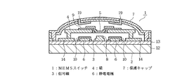
以下、本発明の第1の実施例について、図1ないし図19を参照しながら説明する。まず、図1は本実施例のMEMSスイッチ1の縦断面図であり、図2はMEMSスイッチ1の上面図である。MEMSスイッチ1は、絶縁基板2と、絶縁基板2上に設けられた信号線3と、絶縁基板2上に信号線3をまたぐように設けられた梁4と、梁4に設けられた梁電極5と、絶縁基板2上に設けられた静電電極6と、絶縁基板2上に設けられた保護キャップ7とを備えている。
Hereinafter, a first embodiment of the present invention will be described with reference to FIGS. First, FIG. 1 is a longitudinal sectional view of the MEMS switch 1 of this embodiment, and FIG. 2 is a top view of the MEMS switch 1. The MEMS switch 1 includes an
信号線3は、高周波信号が流れる信号線であり、図8に示すように、分断されており、分断された信号線3の上には、接点電極8(図1参照)が設けられている。梁4の梁電極5は、梁4の下方への変形(撓み変形)に応じて信号線3の接点電極8と接触して信号線3を導通する(即ち、MEMSスイッチ1をオンする)。また、梁電極5は、梁4の復帰変形(上方への変形)に応じて信号線3の接点電極8と開離して信号線3を遮断する(即ち、MEMSスイッチ1をオフする)。
The
上記梁4は、導電性材料で形成されている。静電電極6は、梁4を変形させるための静電気力を発生させるものであり、所定の空間(梁4と静電電極6との間の空間)に電界を発生させる手段を構成している。静電電極6と梁4との間にDC電圧を印加すると、静電気力が梁4に作用し、梁4が下方へ向けて(信号線3の接点電極8に接近する方向へ)撓み変形する。尚、梁電極5と梁4との間には、両者を電気的に絶縁する絶縁体膜9が設けられている。また、静電電極6の上面には、絶縁体膜10が設けられている。
The
一方、保護キャップ7の内面には、キャップ一体静電電極11が設けられている。このキャップ一体静電電極11は、空間(梁4とキャップ一体静電電極11との間の空間)に電界を発生させる手段を構成している。
On the other hand, a cap-integrated
この構成の場合、静電電極6と梁4との間に、DC電圧を印加することを止めると、梁4は上記静電気力の消滅により弾性復元力で上方向に(信号線3の接点電極8から開離する方向に)復帰変形する。このとき、キャップ一体静電電極11と梁4との間にDC電圧を印加すると、静電気力が梁4に作用し、梁4が上方へ向けて(接点電極8から開離する方向へ)復帰変形し易くなる構成となっている。
In this configuration, when the application of the DC voltage between the
次に、上記構成のMEMSスイッチ1を製造する製造プロセスについて、図3ないし図19を参照して説明する。まず、図3(a)に示すように、厚さ500μm程度のシリコン基板12の表面にSiO2等の絶縁膜13を熱酸化処理により形成する。この絶縁膜13の厚さは、電気的な絶縁が確保できるように、500nm〜数μm程度が望ましい。絶縁膜13が形成されたシリコン基板12が絶縁基板2を構成している。
Next, a manufacturing process for manufacturing the MEMS switch 1 having the above configuration will be described with reference to FIGS. First, as shown in FIG. 3A, an
続いて、図3(b)、(c)に示すように、絶縁膜13の上に、Cu、Al、Auなどの導体を成膜し(スパッタや蒸着方法により)、フォトリソグラフィにて信号線3、静電電極6、GND14を形成する。これらの厚さは、例えば1〜数μm程度に設定されている。図3(b)は、静電電極6を形成した状態を示す。図3(c)は、更に信号線3とGND14を形成した状態を示す。尚、図3(b)の静電電極6を形成した状態のシリコン基板12の上面図を、図7に示す。
Subsequently, as shown in FIGS. 3B and 3C, a conductor such as Cu, Al, or Au is formed on the insulating film 13 (by sputtering or vapor deposition), and the signal line is obtained by photolithography. 3. The
そして、図3(d)に示すように、信号線3の上に、AuやPt等の貴金属またはこれらの合金にて信号線3側の接点電極8を形成する。接点電極8の厚さは、数100nm〜1μm程度に設定されている。尚、図3(d)の接点電極8を形成した状態のシリコン基板12の上面図を、図8に示す。
Then, as shown in FIG. 3D, the
更に、図3(e)に示すように、静電電極6上にSiO2等の絶縁体膜10を形成する。絶縁体膜10の厚さは、数150〜300nm程度に設定されている。尚、図3(e)の絶縁体膜10を形成した状態のシリコン基板12の上面図を、図9に示す。
Further, as shown in FIG. 3E, an
上述したようにして、MEMSスイッチ1の下層部分の形成が終了すると、MEMSスイッチ1の特徴である梁4の中空構造を形成する工程を開始する。まず、図4(a)に示すように、第1の犠牲層15を形成する。この第1の犠牲層15は、例えば有機のスピンコートやスプレーコーティング等の塗布工程で形成する、または、ポリシリコン膜等をスパッタやCVDで形成することが良い。第1の犠牲層15の厚みは、接点電極8付近で1μm程度が望ましい。尚、図4(a)の第1の犠牲層15を形成した状態のシリコン基板12の上面図を、図10に示す。
As described above, when the formation of the lower layer portion of the MEMS switch 1 is completed, a process of forming a hollow structure of the
次に、図4(b)に示すように、Al等(導電性材料)によって梁4用の導体膜16を成膜し、梁電極5用の開口部16aを形成する。梁4用の導体膜16の厚みは、1〜数μm程度が望ましい。尚、図4(b)の梁4用の導体膜16を形成した状態のシリコン基板12の上面図を、図11に示す。
Next, as shown in FIG. 4B, the
続いて、図4(c)に示すように、梁電極5用の開口部16aの内面部及び周縁部にSiO2等にて絶縁体膜9を形成する。絶縁体膜9の厚さは、数150〜300nm程度に設定されている。そして、図4(d)に示すように、AuやPt等の貴金属またはこれらの合金によって梁4側の梁電極5を形成する。梁電極5の厚さは、数100nm〜1μm程度に設定されている。尚、図4(d)の梁電極5を形成した状態のシリコン基板12の上面図を、図12に示す。
Subsequently, as shown in FIG. 4C, an
続いて、図4(e)に示すように、梁4用の導体膜15をフォトリソグラフィにてパターニングすることにより、梁4を形成する。尚、図4(e)の梁4を形成した状態のシリコン基板12の上面図を、図13に示す。
Subsequently, as shown in FIG. 4E, the
次に、図5(a)に示すように、保護キャップ7を形成するための第2の犠牲層17を形成する。第2の犠牲層17は、第1の犠牲層15と同様に、例えば有機のスピンコートやスプレーコーティング等の塗布工程で形成する、または、ポリシリコン膜等をスパッタやCVDで形成することも良い。第2の犠牲層17の厚みは、基板面から5μm程度が望ましい。尚、図5(a)の第2の犠牲層17を形成した状態のシリコン基板12の上面図を、図14に示す。
Next, as shown in FIG. 5A, a second
続いて、図5(b)に示すように、第2の犠牲層17上にキャップ一体静電電極11を形成する。この場合、Cu、Al、Auなどの導体を成膜し(スパッタや蒸着方法により)、フォトリソグラフィにてキャップ一体静電電極11を形成する。キャップ一体静電電極11の厚さは、例えば1μm程度に設定されている。尚、図5(b)のキャップ一体静電電極11を形成した状態のシリコン基板11の上面図を、図15に示す。
Subsequently, as shown in FIG. 5B, the cap-integrated
次に、図5(c)に示すように、保護キャップ7用の膜(キャップ膜)18を形成する。このキャップ膜18の材質は、SiO2やSiN等である。キャップ膜18の厚さは、例えば1〜5μm程度に設定されている。続いて、キャップ膜18に電極への引き回し用の孔18aを開ける。尚、図5(c)のキャップ膜18を形成し、孔18aを開けた状態のシリコン基板11の上面図を、図16に示す。
Next, as shown in FIG. 5C, a film (cap film) 18 for the
そして、図5(d)に示すように、電極への引き回し線19を形成する。引き回し線19の材質は、Cu、Al、Auなどの導体である。引き回し線19の厚さは、例えば1μm程度に設定されている。尚、図5(d)の引き回し線19を形成した状態のシリコン基板11の上面図を、図17に示す。
Then, as shown in FIG. 5D, a
続いて、図6(a)に示すように、第1の犠牲層15及び第2の犠牲層17を除去するための除去孔(犠牲層除去用の開口部)20を形成する。尚、図6(a)の除去孔20を形成した状態のシリコン基板11の上面図を、図18に示す。この後、図6(b)に示すように、第1の犠牲層15及び第2の犠牲層17を除去する。この場合、犠牲層15、17が有機のポリイミド膜等であれば、アッシング装置を使用して除去する。尚、犠牲層15、17がポリシリコン膜等であれば、HF等の反応性ガスで除去する。犠牲層15、17を除去した状態のシリコン基板11の上面図を、図19に示す。
Subsequently, as shown in FIG. 6A, a removal hole (opening for sacrifice layer removal) 20 for removing the
ここで、犠牲層15、17を除去する場合に、Wetエッチング法を用いると、犠牲層の除去直後に梁4やキャップ膜18等の中空の構造体が基板12に貼り付いてしまう現象(スティッキング現象)が発生する。このため、ドライエッチングを用いることが望ましい。
Here, when the
この後、図6(c)に示すように、上記除去孔20を塞ぐ(犠牲層除去用の開口部を閉口する)ために、保護キャップ7用の膜(カバー膜)21を形成する。このカバー膜21と前記キャップ膜18とから、保護キャップ7が構成されている。カバー膜21の材質は、SiO2やSiN等である。カバー膜21の厚さは、例えば5μm前後程度に設定することが望ましい。
Thereafter, as shown in FIG. 6C, a film (cover film) 21 for the
上記カバー膜21の形成により、MEMSスイッチ1が完成する。上記カバー膜21を形成した状態のシリコン基板12の上面図を、図2に示す。尚、カバー膜21でキャップ膜18の上面全体を覆うように構成したが、これに代えて、カバー膜を除去孔20の周辺だけに設けて除去孔20を塞ぐように構成しても良い。
By forming the
このような構成の本実施例によれば、静電電極6(電界を発生させる手段)と、梁4と、信号線3とを保護キャップ7で覆って密閉するように構成したので、MEMS構造部分(即ち、梁4の上下面部や周辺部等)にダストや水分が付着することを防止できて、信頼性や歩留りを向上させることができる。
According to the present embodiment having such a configuration, the electrostatic electrode 6 (means for generating an electric field), the
また、上記実施例においては、保護キャップ7の内面にキャップ一体静電電極11を設け、梁4が下方向に撓んだ状態から弾性復元力で上方向に復帰変形するときに、キャップ一体静電電極11と梁4との間に電圧を印加することにより、キャップ一体静電電極11からの電界による静電気力によって梁4を上方向に復帰変形させるように構成したので、接点の粘着をより一層防止することができる。
In the above embodiment, the cap-integrated
更に、上記実施例では、MEMS構造部分を密閉して保護するための保護キャップ7を形成する工程を、半導体プロセス(半導体製造工程)内に設けるように構成したので、製造工程が簡単となり、製造コストを低減することができる。
Furthermore, in the above embodiment, since the process of forming the
尚、上記実施例においては、保護キャップ7の内面にキャップ一体静電電極11を設けたが、これに限られるものではなく、キャップ一体静電電極11を設けることを止めても良い。
In addition, in the said Example, although the cap integrated
また、上記実施例においては、梁4を導電性材料で構成したが、これに代えて、梁4を導電性材料であると共に軟磁性材料である材料(例えばFeSiやNi等)で構成しても良い。
In the above embodiment, the
図20は、本発明の第2の実施例を示すものである。尚、第1の実施例と同一構成には、同一符号を付している。この第2の実施例では、梁4を導電性材料であると共に軟磁性材料である材料(例えばFeSiやNi等)で構成し、更に、保護キャップ7の内面に、キャップ一体静電電極11の代わりにキャップ一体薄膜コイル22を設けた。このキャップ一体薄膜コイル22は、空間(梁4と保護キャップ7との間の空間)に磁界を発生させる手段を構成している。
FIG. 20 shows a second embodiment of the present invention. The same components as those in the first embodiment are denoted by the same reference numerals. In this second embodiment, the
上記構成の場合、梁4が下方向に撓んだ状態から弾性復元力で上方向に復帰変形するときに、キャップ一体薄膜コイル22に通電することにより、キャップ一体薄膜コイル22からの磁気力によって軟磁性材料製の梁4を上方向に復帰変形させる構成となっている。
In the case of the above configuration, when the
尚、上述した以外の第2の実施例の構成は、第1の実施例の構成と同じ構成となっている。従って、第2の実施例においても、第1の実施例とほぼ同じ作用効果を得ることができる。特に、第2の実施例によれば、保護キャップ7の内面にキャップ一体薄膜コイル22を設けたので、梁4が下方向に撓んだ状態から弾性復元力で上方向に復帰変形するときに、キャップ一体薄膜コイル22からの磁気力によって軟磁性材料製の梁4を上方向に復帰変形させることが可能である。
The configuration of the second embodiment other than that described above is the same as that of the first embodiment. Therefore, in the second embodiment, substantially the same operational effects as in the first embodiment can be obtained. In particular, according to the second embodiment, since the cap-integrated
図面中、1はMEMSスイッチ、2は絶縁基板、3は信号線、4は梁、5は梁電極、6は静電電極、7は保護キャップ、8は接点電極、9は絶縁体膜、10は絶縁体膜、11はキャップ一体静電電極、12はシリコン基板、13は絶縁膜、14はGND、15は第1の犠牲層、16は導体膜、16aは開口部、17は第2の犠牲層、18はキャップ膜、18aは引き回し用の孔、19は引き回し線、20は除去孔(犠牲層除去用の開口部)、21はカバー膜、22はキャップ一体薄膜コイルを示す。 In the drawings, 1 is a MEMS switch, 2 is an insulating substrate, 3 is a signal line, 4 is a beam, 5 is a beam electrode, 6 is an electrostatic electrode, 7 is a protective cap, 8 is a contact electrode, 9 is an insulator film, 10 Is an insulating electrode, 11 is a cap-integrated electrostatic electrode, 12 is a silicon substrate, 13 is an insulating film, 14 is GND, 15 is a first sacrificial layer, 16 is a conductor film, 16a is an opening, and 17 is a second electrode. The sacrificial layer, 18 is a cap film, 18a is a routing hole, 19 is a routing line, 20 is a removal hole (sacrificial layer opening), 21 is a cover film, and 22 is a cap-integrated thin film coil.
Claims (5)
前記空間に位置して設けられ、電界による静電気力により下方向に撓み、前記静電気力の消滅により弾性復元力で上方向に復帰変形する導電性材料製の梁と、
前記梁が下方向に撓んだときに電気的に接続される信号線と、
前記電界を発生させる手段と、前記梁と、前記信号線とを覆って密閉する保護キャップとを備えて構成されていることを特徴とするMEMSスイッチ。 Means for generating an electric field in a predetermined space;
A beam made of a conductive material that is provided in the space, bends downward by electrostatic force due to an electric field, and returns and deforms upward by elastic restoring force due to disappearance of the electrostatic force;
A signal line electrically connected when the beam is bent downward;
A MEMS switch comprising: a means for generating an electric field; a protective cap that covers and seals the beam and the signal line.
前記梁が下方向に撓んだ状態から弾性復元力で上方向に復帰変形するときに、前記保護キャップからの電界による静電気力により前記梁を上方向に復帰変形させることを特徴とする請求項1または2記載のMEMSスイッチ。 Means for generating an electric field in the space in the protective cap;
2. When the beam is deformed to return upward by an elastic restoring force from a state in which the beam is bent downward, the beam is restored and deformed upward by an electrostatic force due to an electric field from the protective cap. 3. The MEMS switch according to 1 or 2.
前記梁が下方向に撓んだ状態から弾性復元力で上方向に復帰変形するときに、前記保護キャップからの磁気力により前記梁を上方向に復帰変形させることを特徴とする請求項2記載のMEMSスイッチ。 Means for generating a magnetic field in the space in the protective cap;
3. The beam is deformed in the upward direction by a magnetic force from the protective cap when the beam is deformed in an upward direction by an elastic restoring force from a state in which the beam is bent in the downward direction. MEMS switch.
前記静電電極上に絶縁膜を形成する工程と、
前記絶縁基板上に第1の犠牲層を形成する工程と、
前記第1の犠牲層上に梁用の導体膜を形成する工程と、
前記導体膜上に梁の接点電極を形成する工程と、
前記導体膜上に第2の犠牲層を形成する工程と、
前記第2の犠牲層上に静電電極を形成する工程と、
前記第2の犠牲層上に梁を形成する工程と、
前記梁に前記犠牲層除去用の開口部を形成する工程と、
前記第1及び前記第2の犠牲層を除去する工程と、
前記開口部を閉口する工程とを備えてなるMEMSスイッチの製造方法。 Forming signal lines and electrostatic electrodes on an insulating substrate;
Forming an insulating film on the electrostatic electrode;
Forming a first sacrificial layer on the insulating substrate;
Forming a conductive film for a beam on the first sacrificial layer;
Forming a contact electrode of the beam on the conductor film;
Forming a second sacrificial layer on the conductor film;
Forming an electrostatic electrode on the second sacrificial layer;
Forming a beam on the second sacrificial layer;
Forming an opening for removing the sacrificial layer in the beam;
Removing the first and second sacrificial layers;
And a step of closing the opening.
Priority Applications (2)
| Application Number | Priority Date | Filing Date | Title |
|---|---|---|---|
| JP2007206767A JP2009043537A (en) | 2007-08-08 | 2007-08-08 | Mems switch, and its manufacturing method |
| US12/187,734 US20090071807A1 (en) | 2007-08-08 | 2008-08-07 | Mems switch and method of fabricating the same |
Applications Claiming Priority (1)
| Application Number | Priority Date | Filing Date | Title |
|---|---|---|---|
| JP2007206767A JP2009043537A (en) | 2007-08-08 | 2007-08-08 | Mems switch, and its manufacturing method |
Publications (1)
| Publication Number | Publication Date |
|---|---|
| JP2009043537A true JP2009043537A (en) | 2009-02-26 |
Family
ID=40444075
Family Applications (1)
| Application Number | Title | Priority Date | Filing Date |
|---|---|---|---|
| JP2007206767A Withdrawn JP2009043537A (en) | 2007-08-08 | 2007-08-08 | Mems switch, and its manufacturing method |
Country Status (2)
| Country | Link |
|---|---|
| US (1) | US20090071807A1 (en) |
| JP (1) | JP2009043537A (en) |
Cited By (3)
| Publication number | Priority date | Publication date | Assignee | Title |
|---|---|---|---|---|
| JP2012045656A (en) * | 2010-08-25 | 2012-03-08 | Toshiba Corp | Electrical component and method of manufacturing the same |
| CN107188109A (en) * | 2017-05-26 | 2017-09-22 | 北京有色金属研究总院 | A kind of low driving voltage concave electrodes electrostatic actuator and preparation method |
| CN113226979A (en) * | 2018-12-21 | 2021-08-06 | 罗伯特·博世有限公司 | Sensor device and method for producing a sensor device |
Families Citing this family (12)
| Publication number | Priority date | Publication date | Assignee | Title |
|---|---|---|---|---|
| TW200938479A (en) * | 2007-10-22 | 2009-09-16 | Toshiba Kk | Micromachine device and method of manufacturing the same |
| US8080460B2 (en) | 2008-11-26 | 2011-12-20 | Micron Technology, Inc. | Methods of forming diodes |
| JP2010280035A (en) * | 2009-06-04 | 2010-12-16 | Toshiba Corp | Mems device and method for manufacturing the same |
| US9892879B2 (en) * | 2011-01-11 | 2018-02-13 | Qorvo Us, Inc. | Encapsulated micro-electromechanical system switch and method of manufacturing the same |
| US8569091B2 (en) * | 2009-08-27 | 2013-10-29 | International Business Machines Corporation | Integrated circuit switches, design structure and methods of fabricating the same |
| US8535966B2 (en) | 2010-07-27 | 2013-09-17 | International Business Machines Corporation | Horizontal coplanar switches and methods of manufacture |
| US8946877B2 (en) * | 2010-09-29 | 2015-02-03 | Avago Technologies General Ip (Singapore) Pte. Ltd. | Semiconductor package including cap |
| KR101939175B1 (en) * | 2011-09-02 | 2019-01-16 | 카벤디시 키네틱스, 인크. | Mems device anchoring |
| US20130106875A1 (en) * | 2011-11-02 | 2013-05-02 | Qualcomm Mems Technologies, Inc. | Method of improving thin-film encapsulation for an electromechanical systems assembly |
| US8629036B2 (en) | 2011-11-11 | 2014-01-14 | International Business Machines Corporation | Integrated semiconductor devices with amorphous silicon beam, methods of manufacture and design structure |
| JP2015174150A (en) * | 2014-03-13 | 2015-10-05 | 株式会社東芝 | Mems device and manufacturing method thereof |
| EP3310707A1 (en) | 2015-06-22 | 2018-04-25 | INTEL Corporation | Integrating mems structures with interconnects and vias |
Family Cites Families (7)
| Publication number | Priority date | Publication date | Assignee | Title |
|---|---|---|---|---|
| US6094116A (en) * | 1996-08-01 | 2000-07-25 | California Institute Of Technology | Micro-electromechanical relays |
| US6069540A (en) * | 1999-04-23 | 2000-05-30 | Trw Inc. | Micro-electro system (MEMS) switch |
| US6496612B1 (en) * | 1999-09-23 | 2002-12-17 | Arizona State University | Electronically latching micro-magnetic switches and method of operating same |
| US6440767B1 (en) * | 2001-01-23 | 2002-08-27 | Hrl Laboratories, Llc | Monolithic single pole double throw RF MEMS switch |
| US7280014B2 (en) * | 2001-03-13 | 2007-10-09 | Rochester Institute Of Technology | Micro-electro-mechanical switch and a method of using and making thereof |
| US7463125B2 (en) * | 2002-09-24 | 2008-12-09 | Maxim Integrated Products, Inc. | Microrelays and microrelay fabrication and operating methods |
| TW200938479A (en) * | 2007-10-22 | 2009-09-16 | Toshiba Kk | Micromachine device and method of manufacturing the same |
-
2007
- 2007-08-08 JP JP2007206767A patent/JP2009043537A/en not_active Withdrawn
-
2008
- 2008-08-07 US US12/187,734 patent/US20090071807A1/en not_active Abandoned
Cited By (6)
| Publication number | Priority date | Publication date | Assignee | Title |
|---|---|---|---|---|
| JP2012045656A (en) * | 2010-08-25 | 2012-03-08 | Toshiba Corp | Electrical component and method of manufacturing the same |
| CN107188109A (en) * | 2017-05-26 | 2017-09-22 | 北京有色金属研究总院 | A kind of low driving voltage concave electrodes electrostatic actuator and preparation method |
| CN113226979A (en) * | 2018-12-21 | 2021-08-06 | 罗伯特·博世有限公司 | Sensor device and method for producing a sensor device |
| JP2022514339A (en) * | 2018-12-21 | 2022-02-10 | ロベルト・ボッシュ・ゲゼルシャフト・ミト・ベシュレンクテル・ハフツング | Sensor device and manufacturing method of sensor device |
| JP7177274B2 (en) | 2018-12-21 | 2022-11-22 | ロベルト・ボッシュ・ゲゼルシャフト・ミト・ベシュレンクテル・ハフツング | SENSOR DEVICE AND SENSOR DEVICE MANUFACTURING METHOD |
| CN113226979B (en) * | 2018-12-21 | 2024-04-02 | 罗伯特·博世有限公司 | Sensor device and method for producing a sensor device |
Also Published As
| Publication number | Publication date |
|---|---|
| US20090071807A1 (en) | 2009-03-19 |
Similar Documents
| Publication | Publication Date | Title |
|---|---|---|
| JP2009043537A (en) | Mems switch, and its manufacturing method | |
| US9000494B2 (en) | Micromechanical device and methods to fabricate same using hard mask resistant to structure release etch | |
| US7256670B2 (en) | Diaphragm activated micro-electromechanical switch | |
| JP5449756B2 (en) | MEMS switch with conductive mechanical stopper | |
| US9859076B2 (en) | Encapsulated micro-electromechanical system switch and method of manufacturing the same | |
| JP5193639B2 (en) | Micromachine device and method of manufacturing micromachine device | |
| JP2007535797A (en) | Beam for micromachine technology (MEMS) switches | |
| JP5951344B2 (en) | MEMS device and manufacturing method thereof | |
| EP2200063B1 (en) | Micro-electromechanical system switch | |
| US7851976B2 (en) | Micro movable device and method of making the same using wet etching | |
| US20080174390A1 (en) | Micro-switching device and method of manufacturing the same | |
| US9953787B2 (en) | Dual substrate electrostatic MEMS switch with multiple hinges and method of manufacture | |
| JP5881635B2 (en) | MEMS equipment | |
| JP5784513B2 (en) | MEMS device and manufacturing method thereof | |
| US20210017017A1 (en) | Eight spring dual substrate mems plate switch and method of manufacture | |
| US20190333728A1 (en) | Shielded dual substrate mems plate switch and method of manufacture | |
| JP2009009785A (en) | Mems switch and its manufacturing method | |
| US20160181041A1 (en) | Mems structure with thick movable membrane | |
| JP2009178816A (en) | Micromachine apparatus and method for manufacturing the same | |
| JP2009226501A (en) | Micromechanical apparatus and manufacturing method of micromechanical apparatus |
Legal Events
| Date | Code | Title | Description |
|---|---|---|---|
| A621 | Written request for application examination |
Free format text: JAPANESE INTERMEDIATE CODE: A621 Effective date: 20091001 |
|
| A761 | Written withdrawal of application |
Free format text: JAPANESE INTERMEDIATE CODE: A761 Effective date: 20100416 |