JP2009005391A - Communication system providing hybrid optical/wireless communications and related methods - Google Patents
Communication system providing hybrid optical/wireless communications and related methods Download PDFInfo
- Publication number
- JP2009005391A JP2009005391A JP2008208151A JP2008208151A JP2009005391A JP 2009005391 A JP2009005391 A JP 2009005391A JP 2008208151 A JP2008208151 A JP 2008208151A JP 2008208151 A JP2008208151 A JP 2008208151A JP 2009005391 A JP2009005391 A JP 2009005391A
- Authority
- JP
- Japan
- Prior art keywords
- optical
- optical fiber
- power
- core
- wireless
- Prior art date
- Legal status (The legal status is an assumption and is not a legal conclusion. Google has not performed a legal analysis and makes no representation as to the accuracy of the status listed.)
- Pending
Links
Images


Classifications
-
- H—ELECTRICITY
- H04—ELECTRIC COMMUNICATION TECHNIQUE
- H04B—TRANSMISSION
- H04B10/00—Transmission systems employing electromagnetic waves other than radio-waves, e.g. infrared, visible or ultraviolet light, or employing corpuscular radiation, e.g. quantum communication
-
- H—ELECTRICITY
- H04—ELECTRIC COMMUNICATION TECHNIQUE
- H04B—TRANSMISSION
- H04B10/00—Transmission systems employing electromagnetic waves other than radio-waves, e.g. infrared, visible or ultraviolet light, or employing corpuscular radiation, e.g. quantum communication
- H04B10/25—Arrangements specific to fibre transmission
- H04B10/2575—Radio-over-fibre, e.g. radio frequency signal modulated onto an optical carrier
- H04B10/25752—Optical arrangements for wireless networks
-
- H—ELECTRICITY
- H04—ELECTRIC COMMUNICATION TECHNIQUE
- H04B—TRANSMISSION
- H04B10/00—Transmission systems employing electromagnetic waves other than radio-waves, e.g. infrared, visible or ultraviolet light, or employing corpuscular radiation, e.g. quantum communication
- H04B10/25—Arrangements specific to fibre transmission
Abstract
Description
通信システムは、しばしば、ユーザ間でデータ信号、音声信号、及び/又は、映像信号をルーティングするのに用いられる。 Communication systems are often used to route data signals, audio signals, and / or video signals between users.
典型的な通信システムの1つは、複数のコンピュータ・ワークステーション・ユーザを相互接続するローカル・エリア・ネットワーク(LAN)である。おそらく、LANにおいてコンピュータ又は他の機器を一体に接続する最も一般的な方法は、導線を通じたものである。例えば、コンピュータ・ワークステーションへ接続された壁コネクタ又は床コネクタが建物中に配置され、金属製のワイヤが壁コネクタから例えばそれらがサーバなどのホストコンピュータ装置へ接続にされる1以上の中心位置まで延びる。 One typical communication system is a local area network (LAN) that interconnects multiple computer workstation users. Probably the most common way to connect computers or other equipment together in a LAN is through wires. For example, a wall connector or floor connector connected to a computer workstation is placed in the building, and metal wires extend from the wall connector to, for example, one or more central locations where they are connected to a host computer device such as a server. Extend.
ワイヤによるネットワークの使用にはいくつかの欠点が伴う可能性がある。例えば、電力がワイヤを通じて送信されているため、ワイヤの敷設は、電気コードの影響を受けやすく、敷設をより困難に、或いは、コスト高にさえし得る。さらに、典型的な金属製ワイヤ(例えば、銅線)を用いたときに利用可能な帯域幅は、用途によっては、所望の帯域幅に満たない可能性もある。 The use of a wire network can have several drawbacks. For example, because power is being transmitted over the wire, the laying of the wire is susceptible to electrical cords and can be more difficult or even costly. Furthermore, the bandwidth available when using typical metal wires (eg, copper wire) may be less than the desired bandwidth, depending on the application.
このような制限の結果として、「銅線無しの」ネットワークを提供するために、他の種類の相互接続の利用が試みられている。例えば、光ファイバラインは、電気信号に相当する光信号をコンピュータ又は他の機器間で非常に高速且つ広帯域幅で送信することを可能にする。しかし、光ファイバ通信は、ワイヤより高価であることが多いため、光ファイバラインを数多くの壁コネクタへ延ばすことは、状況によっては、法外なコストが掛かる可能性がある。 As a result of these limitations, other types of interconnections have been attempted to provide a “copper-free” network. For example, optical fiber lines allow optical signals corresponding to electrical signals to be transmitted between computers or other equipment at very high speeds and wide bandwidths. However, optical fiber communication is often more expensive than wires, so extending the fiber optic line to many wall connectors can be prohibitive in some situations.
さらに、光ファイバケーブルは、ワイヤよりも信号を抽出するのが難しい。結果として、光ファイバからの信号抽出の困難性を解決する様々な手法が開発されている。このような手法の1つは、米国特許第6,265,710号に開示されている。この手法によれば、光ファイバから出現した光は、光検出器又は別のガラスファイバの入力面において、集光素子によって方向付けされる。別の手法は、特定の波長の光を捕獲するように物理的に構成された格子を用いることである。この手法の一例は、Pattersonらの米国特許第6,304,696号に開示されている。 Furthermore, optical fiber cables are more difficult to extract signals than wires. As a result, various techniques have been developed to solve the difficulty of signal extraction from optical fibers. One such approach is disclosed in US Pat. No. 6,265,710. According to this approach, light emerging from the optical fiber is directed by the light collecting element at the input surface of the photodetector or another glass fiber. Another approach is to use a grating that is physically configured to capture light of a specific wavelength. An example of this approach is disclosed in US Pat. No. 6,304,696 to Patterson et al.
LANにおいて1以上の機器を相互接続する別の方法は、ワイヤレス通信リンクを用いることである。例えば、LAN内の各機器が、1以上の指定された周波数を用いて、データ信号を他の機器へ送受信するワイヤレス無線周波数(RF)送受信機を有する。この手法は、ワイヤによるネットワーク又は光ファイバによるネットワークに比べて、(もしあれば)壁コネクタがより少なくて済むという利点を有するが、ワイヤレス通信リンクは、機器が様々な場所を移動させられると、干渉や、信号歪みや、信号損失を受ける可能性がある。 Another way to interconnect one or more devices in a LAN is to use a wireless communication link. For example, each device in the LAN has a wireless radio frequency (RF) transceiver that transmits and receives data signals to other devices using one or more specified frequencies. This approach has the advantage of requiring fewer wall connectors (if any) compared to a wire or fiber optic network, but a wireless communication link allows a device to be moved from one location to another. Interference, signal distortion, and signal loss may occur.
以上の背景から、本発明の目的は、光ファイバ通信の利点とワイヤレス通信の利点とを効果的に用いる通信システムを提供することである。 From the above background, an object of the present invention is to provide a communication system that effectively uses the advantages of optical fiber communication and wireless communication.
本発明の上記及び他の目的、特徴、及び利点は、光ファイバと、光ファイバに接続された少なくとも1つの光−ワイヤレス機器とを有する通信システムによって提供される。一例として、上記少なくとも1つの光−ワイヤレス機器は、標準的なファイバコネクタ、上記ファイバ内の格子構造のミクロ製造、電子基板として機能する表面研磨ファイバ、などによって上記ファイバに接続される。さらに、上記光−ワイヤレス機器は、上記光ファイバに接続され、該光ファイバ内の光パワを電力へ変換する光ファイバパワユニットと、該光ファイバパワユニットによって電力が供給され、上記光ファイバに接続されたワイヤレス通信ユニットとを有する。この光−ワイヤレス機器は、上記光ファイバパワユニット及び上記ワイヤレス通信ユニットを上記光ファイバの上記縦側面に取り付ける基板を有する。 The above and other objects, features and advantages of the present invention are provided by a communication system having an optical fiber and at least one optical-wireless device connected to the optical fiber. As an example, the at least one optical-wireless device is connected to the fiber by a standard fiber connector, microfabrication of the lattice structure in the fiber, a surface-polished fiber that functions as an electronic substrate, and the like. Further, the optical-wireless device is connected to the optical fiber, and an optical fiber power unit that converts optical power in the optical fiber into electric power, and power is supplied by the optical fiber power unit, and is connected to the optical fiber. Wireless communication unit. The optical-wireless device includes a substrate for attaching the optical fiber power unit and the wireless communication unit to the vertical side surface of the optical fiber.
上記光ファイバパワユニットは、光起電装置と、該光起電装置を上記光ファイバの上記縦側面に接続するパワ光格子とを有する。上記ワイヤレス通信ユニットは、無線周波数送信器と、該送信器を上記光ファイバの上記縦側面に接続する信号光格子とを有する。 The optical fiber power unit includes a photovoltaic device and a power optical grating that connects the photovoltaic device to the vertical side surface of the optical fiber. The wireless communication unit includes a radio frequency transmitter and a signal light grating that connects the transmitter to the vertical side of the optical fiber.
本発明の別の重要な態様によれば、上記無線周波数送信器は、超広帯域送信器を有する。この超広帯域送信器は、上記信号光格子に接続された入力を備えた光検出器と、この光検出器の出力に接続された入力を備えた増幅器と、擬似ランダムコード生成器と、該増幅器及び該擬似ランダムコード生成器の出力に接続された入力を備えたマルチプレクサと、該マルチプレクサの出力に接続された入力を備えたパルス発生器とを有する。 According to another important aspect of the invention, the radio frequency transmitter comprises an ultra wideband transmitter. The ultra-wideband transmitter includes a photodetector with an input connected to the signal light grating, an amplifier with an input connected to the output of the photodetector, a pseudo-random code generator, and the amplifier And a multiplexer with an input connected to the output of the pseudo-random code generator, and a pulse generator with an input connected to the output of the multiplexer.
また、上記超広帯域送信器は、上記パルス発生器の出力に接続されたアンテナを有する。一例として、このアンテナは、例えばダイポールアンテナである。特にコンパクトで効率的な構造とするために、このダイポールアンテナは、上記光ファイバの上記縦側面に沿って反対方向に延びる第一の部分及び第二の部分を有することが好ましい。 The ultra wideband transmitter has an antenna connected to the output of the pulse generator. As an example, this antenna is, for example, a dipole antenna. In order to achieve a particularly compact and efficient structure, the dipole antenna preferably has a first portion and a second portion that extend in opposite directions along the longitudinal side of the optical fiber.
上記光ファイバは、コアと、該コアを囲むクラッドとを有する。したがって、上記光ファイバパワユニット及び上記ワイヤレス通信ユニットは、上記光ファイバの上記コアに接続される。 The optical fiber has a core and a clad surrounding the core. Therefore, the optical fiber power unit and the wireless communication unit are connected to the core of the optical fiber.
上記ワイヤレス通信ユニットがワイヤレス送信器を有する実施形態において、上記システムは、更に、上記ワイヤレス送信器から離間され、該ワイヤレス送信器から信号を受信する少なくとも1つのワイヤレス受信器を有する。逆に、上記ワイヤレス通信ユニットがワイヤレス受信器を有する実施形態において、上記システムは、上記ワイヤレス受信器から離間され、該ワイヤレス受信器へ信号を送信する少なくとも1つのワイヤレス送信器を有する。当然、更に別の実施形態として、全二重通信が提供されてもよい。 In embodiments where the wireless communication unit comprises a wireless transmitter, the system further comprises at least one wireless receiver spaced from the wireless transmitter and receiving a signal from the wireless transmitter. Conversely, in an embodiment where the wireless communication unit has a wireless receiver, the system has at least one wireless transmitter that is spaced from the wireless receiver and transmits a signal to the wireless receiver. Of course, as yet another embodiment, full duplex communication may be provided.
上記通信システムは、特に、銅線無しネットワークに適用できる。上記実施形態において、上記少なくとも1つの光−ワイヤレス機器は、上記光ファイバの上記縦側面に沿って間隔を空けて上記光ファイバに接続された複数の光−ワイヤレス機器を有し得る。状況によっては、複数の光−ワイヤレス機器を上記光ファイバに接続することができる。 The communication system is particularly applicable to a copper wire-free network. In the above embodiment, the at least one optical-wireless device may comprise a plurality of optical-wireless devices connected to the optical fiber spaced along the longitudinal side of the optical fiber. In some situations, multiple optical-wireless devices can be connected to the optical fiber.
上記光−ワイヤレス機器における電力供給及び信号送出には異なる光波長を用いることができる。特に、上記ワイヤレス通信ユニットが第一の光波長で作動し、上記システムが、上記光ファイバに接続され、上記光ファイバパワユニットに電力を供給すると共に、上記第一の光波長とは異なる第二の波長で作動する光パワ発生源を有する、ようにすることができる。加えて、異なる光波長の代わりに、上記光−ワイヤレス機器は、異なるモード、異なる極性、又は異なるコードで作動する、或いは、何らかの別の方法で光−ワイヤレス機器間で信号及び電力を異ならせることも可能である。 Different light wavelengths can be used for power supply and signal transmission in the optical-wireless device. In particular, the wireless communication unit operates at a first optical wavelength, the system is connected to the optical fiber, supplies power to the optical fiber power unit, and is different from the first optical wavelength. Having an optical power source operating at a wavelength of. In addition, instead of different optical wavelengths, the optical-wireless device can operate in different modes, different polarities, or different codes, or in some other way different signals and power between the optical-wireless device. Is also possible.
本発明の方法態様は、光−ワイヤレス通信用である。この方法は、光ファイバパワユニットと該光ファイバパワユニットに接続されたワイヤレス通信ユニットを有する少なくとも1つの光−ワイヤレス機器を光ファイバの縦側面に接続する。本方法は、更に、該光ファイバ内に光パワを供給し、上記光ファイバパワユニットを用いて、該光ファイバ内の光パワを電力へ変換し、該光パワから変換された該電力を用いて、光−ワイヤレス通信のために上記ワイヤレス通信ユニットに電力を供給する。加えて、例えば、太陽電池や、整流アンテナなどの方法によって、或いは、導線によって、外部電力が供給されてもよい。 The method aspect of the present invention is for optical-wireless communication. The method connects at least one optical-wireless device having an optical fiber power unit and a wireless communication unit connected to the optical fiber power unit to a longitudinal side of the optical fiber. The method further supplies optical power into the optical fiber, converts the optical power in the optical fiber into electric power using the optical fiber power unit, and uses the electric power converted from the optical power. Then, power is supplied to the wireless communication unit for optical-wireless communication. In addition, for example, external power may be supplied by a method such as a solar cell or a rectifying antenna, or by a conductive wire.
以下、本発明の好ましい実施形態が図示された添付図面を参照して、本発明をより完全に説明する。しかしながら、本発明は、多くの異なる形で具現化できるものであって、ここに説明する実施形態に限定されるものとして解釈されるべきではない。むしろ、これら実施形態は、この開示をより完全なものとし、本発明の範囲を当業者に完全に伝えるために提供されている。全体を通して同じ数字は同じ要素を示し、代替的実施形態における類似の要素を示すのにはプライム表記法が用いられる。 The present invention will now be described more fully hereinafter with reference to the accompanying drawings, in which preferred embodiments of the invention are shown. However, the present invention can be embodied in many different forms and should not be construed as limited to the embodiments set forth herein. Rather, these embodiments are provided so that this disclosure will be thorough and complete, and will fully convey the scope of the invention to those skilled in the art. Throughout, the same numbers indicate the same elements, and prime notation is used to indicate similar elements in alternative embodiments.
最初に図1を参照する。本発明に係る通信システム10は、一例として、光ファイバ11と、光ファイバの縦側面に沿って1以上のポイントに接続された少なくとも1つの光ワイヤレス機器12とを有する。例えばLANの場合、光ファイバ11は、PDA13、携帯電話14、及び/又は、パソコン15などの電子機器がアクセスを必要とするサーバ16又は他の中央データソース/ノードへ接続される。当然、当業者には明らかなように、本発明に係る通信システム10は、LAN以外の数多くの用途に用いることが可能であり、また、上記以外の種類の電子機器と共に用いることも可能である。
Reference is first made to FIG. The communication system 10 according to the present invention includes, as an example, an
したがって、当業者には明らかなように、通信システム10は、特に、銅線無しのネットワークに適用できる。このような実施形態において、複数の光ワイヤレス機器12a、12b、12cは、例えば、光ファイバの縦側面に沿って間隔を空けて光ファイバ11に接続される。光ワイヤレス機器12a、12b、12cは、PDA13、携帯電話14、及び、パソコン15とそれぞれワイヤレス通信を行うのに用いられる。後により完全に説明するように、光ワイヤレス機器12は、有益的なことに、光ファイバ11上で(例えばサーバ16によって)送信された光信号をワイヤレス信号へ変換して、それを個々の電子機器へ送信するのに用いることができる。逆に、光ワイヤレス機器12は、図1に矢印で例示するように、個々の電子機器から送信されたワイヤレス信号を対応する光信号へ変換してそれを光ファイバ11上で(例えばサーバ16へ)送信することもできる。
Thus, as will be apparent to those skilled in the art, the communication system 10 is particularly applicable to networks without copper wires. In such an embodiment, the plurality of optical
本発明の光ワイヤレス機器12の結果として、通信システム10は、有益的なことに、光通信とワイヤレス通信のいくつかの利点を、それらの個別の欠点の一部を回避しながら、実現することができる。より具体的には、1以上の光ファイバ11を用いて、物理的ネットワークエリア(例えば、建物の床や船、など)全体の至るところのサーバ16又は他の中央データソースからの信号を、光ファイバを延ばすことなく、数多くのワークステーション接続ポイントへルーティングすることができる。
As a result of the
さらに、光信号が劣化を最小に抑えながら光ファイバを通じて比較的長い距離を移動することができるため、通信システム10が達するレンジが、単なるワイヤレスネットワークよりも大幅に広がり、さらには、ワイヤレス信号中継局を必要とせず、建物間にも拡張することもできる。加えて、光ワイヤレス機器12と個々の電子機器との間で送信されるワイヤレス信号は、一般的に、単なるワイヤレスネットワークの場合ほど遠くまで飛ぶ必要がない(すなわち、それらはすぐ近くの光ファイバ11へ飛べばよく、サーバ16までのすべての行程を飛ぶ必要はない)ため、干渉及び信号歪みも低減する潜在的可能性がある。
Further, since the optical signal can travel a relatively long distance through the optical fiber while minimizing degradation, the range reached by the communication system 10 is significantly wider than a simple wireless network, and further, a wireless signal relay station Can also be extended between buildings. In addition, wireless signals transmitted between the
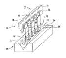
次に、図2〜4を参照する。ここでは、光ワイヤレス機器12についてより詳細に説明する。光ファイバ11は、一例として、当業者には明らかなように、コア23と、コアを囲むクラッド24とを有する。光ワイヤレス機器12は、一例として、コア23に接続され、後述するように光パワを電力に変換する光ファイバパワユニット20を有する。
Reference is now made to FIGS. Here, the
さらに、ワイヤレス通信ユニット25も、光ファイバ11のコア23に接続され、光ファイバパワユニット20から電力供給を受けることができる。図2に示すような実施形態などでは、光ファイバパワユニット20の一部とワイヤレス通信ユニット25の一部とが単体の機器として具現化されてもよい。よって、図2の破線は、1つの光ワイヤレス機器12において2つの別々の機能が実行される場合を示すためのものであって、様々な回路構成要素の特段の細分化又は配置は必要ない。
Further, the
光ファイバパワユニット20は、一例として、1以上の光起電装置21と、光ファイバ11のコア23から発電に用いられる光を特に抽出するように指定された個別の光格子22とを有する。したがって、パワ光格子22は、ワイヤレス通信機器25用の電力へ変換される特定の光波長λ1を有する光をコア23から抽出するように「チューニングされる」ことが好ましい。当業者には明らかなように、発電用の光を抽出するためのミクロ光学構造は、特定の波長、極性、モード等に「チューニングする」ことができる。当業者には明らかなように、光ファイバパワユニット20は、図5及び6に概略的に示すように、必要に応じてパワ調整回路が追加されてもよい。
The optical
光起電装置21として用いることが可能な具体的な種類の一例は、感光性表面上に広帯域反射防止コーティングが施された比較的広域に平面拡散したInGaAs光ダイオードである。このようなダイオードは、当業者には既知である。いくつかのこのような光起電装置21は、(例えば図5及び6に示すように)直列につなげて、ワイヤレス通信ユニット25に電力を供給し、その光信号検出器26(後述)を逆バイアスするのに必要な電圧を生成することができる。光ダイオード21は、照射効率が最適化されるように、個々の格子22上に配置されることが好ましい。
An example of a specific type that can be used as the
当業者には明らかなように、光ダイオードの照射効率を最適化するためには、コア23から抽出された光のうち光ダイオード21の空乏領域内で吸収される量を最大にすることが重要である。コア23から抽出され、空乏領域において吸収されない光は、損失及び効率の低下を表す。損失の原因は、例えば、反射、方向付けが誤った又は集光されなかった光、空乏領域外での光量子吸収、などである。当業者には明らかなように、反射防止コーティング、接合点方向付け、及び、ビーム集光は、損失を最小化するために、個々のデザイン用途に応じて調整することができる。
As will be apparent to those skilled in the art, in order to optimize the irradiation efficiency of the photodiode, it is important to maximize the amount of light extracted from the core 23 that is absorbed in the depletion region of the
光ダイオード21を照射する手法の一例は、光ダイオード接合点に垂直に光を入射させることである。別の手法は、光ダイオード21の接合点に平行に光を入射させることである。後者の手法は、接合点をコア23の長さ方向に沿って並べることができるという利点を有する。これにより、より長い格子22に例えば強化機能を与えることができる。当業者には明らかなように、他の手法も潜在的に用いることができる。
An example of a method for irradiating the
また、明らかなように、電源から負荷へ最大の電力を伝達するためには、負荷抵抗と等価な発生源抵抗とを等しくすることが好ましい。照射している間、開回路負荷に接続された光ダイオードは、光電圧VOCを産み出す。同様に、短絡回路負荷に接続された光ダイオードは、光電流ISCを産み出す。このとき、光ダイオードの等価な発生源抵抗REQは、約VOC/ISCである。当業者には明らかなように、光ワイヤレス機器12へのパワ伝達を最適化するために、発生源抵抗及び負荷抵抗は、それぞれの用途に応じて、最適な一致が実現されるように調整されることが好ましい。
Further, as is clear, in order to transmit the maximum power from the power source to the load, it is preferable to make the load resistance and the equivalent source resistance equal. During illumination, the photodiode connected to the open circuit load produces a photovoltage VOC. Similarly, a photodiode connected to a short circuit load produces a photocurrent ISC. At this time, the equivalent source resistance REQ of the photodiode is approximately VOC / ISC. As will be apparent to those skilled in the art, in order to optimize power transmission to the
光ダイオードの照射を最適化することに加えて、パッケージ化することによって電気的相互接続に導入された寄生インピーダンスが最小限に保たれることが好ましい。当業者には明らかなように、電源コネクタにおける寄生インピーダンスは、パワ変換効率を低減させる。送信器27とアンテナ34(図3)との間の寄生インピーダンスが放射パルスの帯域幅及び/又は形状を過度に制限しないようにも気を付ける必要がある。本発明では様々な種類の相互接続を用いることができ、その選択基準は、例えば、シンプルで、安価で、大量生産できるものであること、などである。
In addition to optimizing the illumination of the photodiode, packaging preferably keeps the parasitic impedance introduced to the electrical interconnect to a minimum. As will be apparent to those skilled in the art, the parasitic impedance in the power connector reduces the power conversion efficiency. Care must also be taken that the parasitic impedance between the
電気的相互接続を形成するこのような手法の1つは、導電性エポキシを用いることである。このようにして相互接続を形成することは、本分野では良く知られており、ワイヤボンディングより低い寄生インダクタンスを有し、他の従来の相互接続よりも占める物理的空間が少ない。また、このエポキシによる相互接続の形成は、機器を所定の場所に永久的に保持することができる。加えて、添加物を用いてエポキシの導電性を変え、信号検出ダイオード26をバイアスするのに用いられる抵抗39(図3)を形成することができる。これが可能であるのは、信号検出器回路のバイアス抵抗39に必要なパワが非常に低いためである。さらに、非導電性エポキシ44を用いて、光ダイオード21を1以上の信号検出ダイオード26から絶縁することも可能である。
One such technique for forming electrical interconnects is to use a conductive epoxy. Forming interconnects in this manner is well known in the art, has a lower parasitic inductance than wire bonding, and occupies less physical space than other conventional interconnects. Also, this epoxy interconnect formation can permanently hold the device in place. In addition, additives can be used to change the conductivity of the epoxy to form a resistor 39 (FIG. 3) that is used to bias the
エポキシを多機能に用いることにより、パッケージの複雑さ、サイズ、組立に必要な処理工程数、及び、コストを減らすことができる。ワイヤボンディングを用いることがより適切な場合、それに関連する寄生は最小限に保たれることが好ましい。ワイヤボンディングは、注意しなければ、ナノヘンリー(nano−Henry)レベルのインダクタンスを容易にパッケージ内に導入する可能性がある。ワイヤボンディングの寄生を減らす方法の1つは、パッケージ19又は基板43(図4)へ向けてボンドを平らに押圧することである。これは、ワイヤが曲がるのを制限して磁束鎖交を減らし、ワイヤをグランド面に近づけて、より制御されたインピーダンスを有する送信ラインとして機能させる。
By using epoxy in multiple functions, the complexity, size, number of processing steps required for assembly, and cost can be reduced. Where it is more appropriate to use wire bonding, the associated parasitics are preferably kept to a minimum. Wire bonding can easily introduce nano-henry level inductance into the package if care is not taken. One way to reduce wire bonding parasitics is to press the bond flat against the
特に、ワイヤボンド40は、上述のように、光ダイオード21を直列に連結するのに用いることができ、ワイヤボンド41は、光パワファイバユニット20をワイヤレス通信ユニット25へ連結するのに用いることができる。加えて、ワイヤボンド42a、42bは、ワイヤレス通信ユニット25をダイポールアンテナ素子34a、34b(図1)に連結するのに用いることができる。
In particular, the
ワイヤレス通信ユニット25は、一例として、無線周波数(RF)送信器27と、ファイバ11から光データ信号を抽出するのに最適化された光信号格子28とを有する。当然、光信号格子28及びパワ格子22は、それぞれに異なって最適化されてもよい。本発明の重要な態様の1つにおいて、RF送信器27は、超広帯域(UWB)送信器である。UWBは、非常に広い周波数帯域にわたった非常に低電力のスペクトル密度に拡散されたワイヤレス通信を提供する。データは、RFエネルギの離散パルスを変調し、放射することによって、送信される。結果として、UWBは、通信システム10において使用すると特に有益的となる。なぜなら、UWBは、多くの既存の持続波挟帯域システムと干渉無しで共存できるからである。さらに、UWBパルスの広スペクトル性質及び/又は低周波含有により、UWBパルスは、他の既存の技術よりも壁及び障害物を貫通するのにより良く適している。当然、当業者には明らかなように、他の形のワイヤレス通信も本発明において用いることができる。
As an example, the
図3に一例を示すように、超広帯域送信器27は、例えば、信号光格子(図2)に連結された入力を備えた光信号検出器26を有する。また、信号検出器26は、例えば、上述のInGaAs光ダイオードなどの光ダイオードである。上述の光ダイオード21の配置や効率等に関する考察は、光ダイオード26にも適用可能であるため、光ダイオード26は複数個用いることもできるが、信号を検出するのには通常1つだけで十分であることに注意する以外については、説明を省略する。さらに、ワイヤレス通信ユニット25が半導体技術を用いて実現された実施形態には、半導体技術を用いて実現することが可能な信号調整回路(図示せず)が更に含まれてもよい。
As shown in FIG. 3, for example, the
増幅器30は、光検出器26の出力に接続された入力を有する。送信器は、更に、擬似ランダムコード生成器31と、増幅器30及び擬似ランダムコード生成器31の出力に接続された入力を備えたマルチプレクサ32と、マルチプレクサの出力に接続された入力を備えたパルス発生器33とを有する。当業者には明らかなように、他のUWB送信器回路構成も可能である。
また、超広帯域送信器27は、パルス発生器33の出力に接続されたアンテナ34も有する。一例として、アンテナ34は、超広帯域送信器27(又は他の適切なRF機器)にワイヤボンド42a、42b(図1)によって接続されたダイポールアンテナである。特にコンパクトで効率的な構造のために、ダイポールアンテナ34は、図2に一例を示すように、光ファイバ11の縦側面に沿って反対方向に延びる第一の部分34aおよび第二の部分34bを有することが好ましい。
The ultra
低いプロファイルを維持するために、光ファイバ側に内蔵可能な広帯域ダイポールアンテナ34を用いることが好ましい。しかし、当業者には明らかなように、ほとんどのダイポールアンテナは内在的に狭い帯域を有する。なぜなら、それらは定常波をサポートする共鳴構造だからである。したがって、様々な手法を用いて、超広帯域送信をより効率的にサポートするようにダイポールアンテナ34の帯域幅を増加させることができる。このような手法の1つは、アンテナの電流分布が進行波をサポートするように変更される進行波法である。
In order to maintain a low profile, it is preferable to use a
より具体的には、ダイポールを作るのに抵抗材を用いることによって入力端子からの距離を減らすように電流波の振幅が作られる。アンテナ34は、電流分布がアンテナの性能に深刻な影響を与えないような微小となるポイントにおいて、切断されてもよい。ダイポール端点から反射される電流はほとんどないため、共鳴が回避され、この構造は進行波をサポートする。この手法は、帯域幅を向上させるが、アンテナ34におけるエネルギ損失のために効率が犠牲にされる可能性がある。当業者には明らかなように、アンテナ34の抵抗プロファイルは、用途によっては、効率と帯域幅の間のトレードオフを最適化するために長さ方向に沿って変える必要があるかもしれない。この手法に関する更なる情報は、Tonnら、「Traveling Wave Microstrip Dipole Antennas」、IEEE Electronics Letters、volume 31、issue24、1995年11月23日、2,064〜2,066頁、から得ることができる。
More specifically, the amplitude of the current wave is made to reduce the distance from the input terminal by using a resistive material to make the dipole. The
更に別の手法は、ダイポールの有効長を周波数依存にすることによって寄生を意図的に導入して周波数応答を広げるインピーダンス・ローディング(impedance loading)法である。これは、高周波が多重共鳴するのを防止し、それらをダイポールのより小さい一部分の範囲に限定することによって、達成される。ここで、再び、この手法は、寄生負荷のエネルギ損失のせいで、効率を犠牲にして帯域幅を向上させることができる。したがって、アンテナ34のインピーダンス・プロファイルは、用途によっては、効率と帯域幅との間のトレードオフを最適化するために、長さ方向に沿って変える必要があるかもしれない。この手法に関する更なる情報は、Austinら、「Numerical modeling and design of loaded broadband wire antennas」、IEEE Fourth International Conference on HF Radio Systems and Techniques、1988年、125〜129頁、に記載されている。
Yet another approach is an impedance loading technique that intentionally introduces parasitics to broaden the frequency response by making the effective length of the dipole frequency dependent. This is accomplished by preventing multiple resonances of the high frequency and limiting them to a smaller portion of the dipole. Here again, this approach can increase bandwidth at the expense of efficiency due to parasitic load energy loss. Thus, the impedance profile of
したがって、当業者は、上記の(又は他の)手法のうちいずれが本発明の特定の実施にあたって最も適切なものとなり得るかを判断する必要があるかもしれない。加えて、アンテナのインピーダンス・プロファイル及び/又は抵抗プロファイルは、帯域幅及び効率以外の理由によって調整することも可能である。プロファイルは、パルス成形や信号フィルタリングなどの機能に対して設計・最適化することができる。 Accordingly, one skilled in the art may need to determine which of the above (or other) approaches may be most appropriate for a particular implementation of the present invention. In addition, the impedance and / or resistance profile of the antenna can be adjusted for reasons other than bandwidth and efficiency. Profiles can be designed and optimized for functions such as pulse shaping and signal filtering.
上述のように、本発明の一態様によれば、パワ光格子22を用いてコア23からワイヤレス通信ユニット25へ光が抽出されると共に、光信号格子28を用いてコアから光を抽出する(ワイヤレス通信からの信号送信の場合)又はコアへ光を案内する(すなわち、ワイヤレス通信ユニットによる信号受信の場合)。当然、当業者には明らかなように、消散結合(evanescent coupling)や、パワ分離や、さらには複数のファイバなど、光ファイバ11から光を抽出する他の手法も存在する。これらの手法及び当業者には既知の他の適切な手法も、本発明の範囲内に含まれる。
As described above, according to one aspect of the present invention, light is extracted from the core 23 to the
光ワイヤレス機器12における電力供給及び信号送出には様々な光波長が用いられることが好ましい。特に、ワイヤレス通信ユニット25は、光信号発生源35(図5)によって(ワイヤレス通信ユニットによる送信の場合に)供給された光波長λ2の光で作動可能である。この場合、光信号格子28は、後述するように、λ2に「チューニング」される。さらに、通信システム10は、光ファイバ、特にコア23に接続され、上述のように、波長λ1の光を用いて光ファイバパワユニット20に電力を供給する光パワ発生源36を有することができる。当然、実施形態によっては、同じ波長の光の単一の発生源から信号と電力の双方を抽出することが可能となり得る。光パワ発生源36及び光信号発生源35は、例えばサーバ16の内部回路であってもよい。
Various optical wavelengths are preferably used for power supply and signal transmission in the
ここで、格子22及び28の製造について詳細に説明する。製造工程を円滑にするために、ファイバベンチ(fiber bench)29が用いられると有益的である。ファイバベンチは、クラッド24の一部を削ぎ落としてファイバコア23の非常に近くに平らな面が形成されたファイバの一部分である。当業者には明らかなように、ファイバベンチ29上に製造された表面格子22、28は、スペクトルフィルタリング、分散補償、モードマッチング、モードストリッピング、光抽出/注入、などの様々な機能を実行するために消散フィールド(evanescent field)を利用することができる。また、格子22、28は、これら機能を他に影響を与えずに、特定の波長(例えば、λ1及びλ2)又は特定のモード上で実行するように設計することもできる。
Here, the manufacture of the
このように光ファイバ11とのインターフェイスをとることは、挿入損失が低くなり、システムの複雑さが低減し、機能性が強化され、大量生産の可能性がある、といった利点を有する。このようにしていない従来の接続では、様々な波長で作動する複数の光ワイヤレス機器12を用いるときに光ファイバ11の損失が大きくなる可能性があった。また、ファイバベンチ29は、特定の実施形態では、MEMSや、センサ(例えば、生化学センサ、音響センサ、地震センサ、など)や、他のミクロシステムなどの小型デバイスを受け入れるミクロサイズの基板として用いることもできる。
Taking an interface with the
ファイバベンチ29は、ファイバをシリコンV字溝に置き、隙間をエポキシで埋めることによって作ることができる。エポキシを硬化させると、光ファイバ11のクラッド24がコア23の近くになるまでアッセンブリ全体が磨かれる。次いで、例えば液滴テスト測定を用いて、ファイバベンチ29表面からファイバコア23までの近さを精密に制御する。この工程は、自動化することができるため、ファイバベンチを備えたシステムは、低コストで大量生産することができる可能性がある。ファイバベンチの使用法に関する更なる詳細については、例えば、Leminger and Zengerle、Journal of Lightwave Technology、Volume 3、1985年、などを参照のこと。
The
この手法の更なる利点は、機器にシリコンベンチ29部分を用いて検出器エレクトロニクスと一体化することができることである。さらに、当業者には明らかなように、ファイバベンチ29のシリコン部分上に更なる光学素子及び/又はアンテナ素子(図示せず)を一体的に追加することが可能であると便利である。
A further advantage of this approach is that the instrument can be integrated with detector electronics using a
液滴テスト測定法は、ファイバベンチ29表面の光ファイバ11のコア23に対する近さを評価する。光は、光ファイバ11の一端へ注入され、ファイバベンチ29の領域を通って、最終的にはパワメータへ伝搬する。液体の一滴をファイバベンチ29表面上に置くことによって、光は、液体の領域から外れ、パワメータによって損失として測定することができる。光損失の一部は、ベンチ表面からファイバコアまでの距離を演算するのに用いることができる。
The droplet test measurement method evaluates the proximity of the surface of the
格子22、28を製造する1つの方法は、コア形成中にコアを傾けることである。当業者には明らかなように、格子は、その分散特性のために内在的にスペクトルを選択でき、コア23からの波長の帯域を選択的に再度方向付けるように設計することができる。外れた光は、次いで、光ファイバ11の平らな側面上に製造されたミクロ光素子を用いて、光ダイオード21、26上に集光される。この手法は、コア23に隣接する格子22、28を作るのに感光性ガラスを必要とするため、屈折率の大きな変化を実現することが困難となる可能性がある。屈折率の変化が小さいと、ファイバから大量の光パワを取り出すのに長いインタラクション長さを必要とする。これは、集光を複雑すると共に、ミクロパッケージングにするというオプションを制限する可能性がある。
One method of manufacturing the
したがって、例えば標準的なリソグラフィック工程を用いて、表面格子22、28は、それらを光ファイバ11の研磨面上にエッチングすることによって製造される。インタラクション長さを減らすために、格子構造の表面に高い屈折率の物質を上塗りすることによって屈折率変化を大幅に強化することが可能である。
Thus, for example, using standard lithographic processes, the
また、傾けられた表面格子構造は、光抽出及び光ダイオード照射効率を最適化するのに用いることができる可能性がある。これは、光ファイバ11を傾けられた固定物上に置き、異方性エッチングパターンをファイバベンチ29表面に用いることによって、実現可能である。この手法により、例えば0〜30°の傾斜角を得ることができる。集光光学系を追加する必要がないように、格子構造22、28のインタラクション長さは、それぞれ光ダイオード21、26のアクティブ領域より長くないことが好ましい。このように、取り出された光は、内在的に、アクティブ領域の面積に制限される。追加的な集光が必要となった場合、当業者には明らかなように、回折光学系を用いて、光を光ダイオード21、26上へ集光してもよい。
In addition, the tilted surface grating structure may be used to optimize light extraction and photodiode illumination efficiency. This can be achieved by placing the
上記の光を抽出する手法は、光ファイバ11から出て案内された光を電力抽出及び信号抽出のために特定の波長又はモードから再方向付け又はタッピングすることに基づくものである。別の手法は、この問題をスペクトル選択式方向性カプラとして考える。ファイバコア23及び光ダイオード基板は、伝搬する光の2つ領域を表す。当業者には明らかなように、これら2つの領域を近づけることによって、スペクトル選択式格子をこれら2つの領域の伝搬定数にマッチするように設計することによってファイバからの光を非常に効率的に光ダイオードへ接続することが可能となり、方向性カプラを効率的に形成することができる。
The above-described light extraction technique is based on redirecting or tapping light guided out of the
上述のように、信号用の光と電力は、波長選択式格子22、28を用いることによって、異なる波長λ1、λ2上で提供することができるため、電力及び信号光は別々に抽出することができる。別の手法として、信号用光と電力を異なる伝播モードで提供してもよい。例えば、この目的に適しているであろう段階的屈折率マルチモードの個々のモードをエキサイトさせるボルテックスレンズを用いるプロセスが開発されている。このプロセスは、Johnsonら、「Diffractive Vortex Lens for Mode−Matching Graded Index Fiber」、Optical Society of America、Topical Meeting on Diffractive and Micro−Optics、2000年、に記載されている。よって、当業者には明らかなように、回折光学系を用いて電力用波長λ1及び信号用波長λ2について光を異なる空間モードへ送り出すことも実現可能性があると言える。同様に、回折光学系は電力モード及び信号モードをそれぞれ空間的に逆多重化するように設計することも潜在的に可能であることは明らかである。
As described above, signal light and power can be provided on different wavelengths λ 1 , λ 2 by using the wavelength
別の手法として、一方のファイバが電力供給専用で、他方のファイバが信号を分配する二重ファイバアッセンブリを利用してもよい。これは、信号ファイバを妨害せずに、ネットワークの様々な場所において、電力チャネルを増幅又は再供給することができるという点でいくつかの利点を有する。このようにして電源を分散させることができるため、通信システム10をより信頼性が高く、より強力なものとすることができる。さらに、当業者には明らかなように、光ファイバ11を使うため、例えば、波長分割多重(WDM)方式や、高密度波長分割多重(DWDM)方式が採用できる。この手法は、標準的なパッシブWDM技術及び電力チャネルに対して標準的な増幅器技術を用いることによって、様々な信号を分配することができる。しかし、この一体化は、潜在的に、上述のシングル光ファイバ手法よりも多くの土地を必要とする。当然、両実施形態とも本発明の範囲内に含まれるものであり、実施形態によっては電力を供給するのに別体の導線を用いることさえもできることは明らかである。
Alternatively, a duplex fiber assembly may be utilized in which one fiber is dedicated to supplying power and the other fiber distributes the signal. This has several advantages in that the power channel can be amplified or re-supplied at various locations in the network without disturbing the signal fiber. Since the power supply can be distributed in this way, the communication system 10 can be made more reliable and more powerful. Further, as will be apparent to those skilled in the art, since the
上述のように、光ワイヤレス機器の一部は、パッケージング19(図2)を備えた半導体機器として実施されると有益的である。この実施形態では、パッケージング19は、光ファイバパワユニット20及びワイヤレス通信ユニット25を光ファイバ11の縦側面に対してマウントする基板として機能することができる。図4に示した実施形態のように、この目的のために別体の基板43(例えば、セラミック基板)を用いることも可能である。
As mentioned above, some of the optical wireless devices are beneficially implemented as semiconductor devices with packaging 19 (FIG. 2). In this embodiment, the
図4に示した1つの考えられるミクロパッケージング手法は、様々なハードウェア部分をモジュール化することを含む。特に、光ダイオード21、26の行が、セラミック基板43の前面に固定される。基板43の背面には、上述のUWB無線ハードウェアが設けられている。電気的相互接続は、同じく上述のように、導電性抵抗エポキシ、セラミック基板の金属製軌跡、及び、ワイヤボンドによって提供される。この構成において、例えば、セラミック基板及びシリコン基板を一体に「スナップ」させてもよい。
One possible micro-packaging approach shown in FIG. 4 involves modularizing the various hardware parts. In particular, the rows of
これも上述したように、光ワイヤレスユニット12は、ワイヤレス信号を送信も受信もすることができる。ワイヤレス通信ユニット12がワイヤレス送信器27を有する実施形態において、通信システム10は、更に、一例を図5に示すように、ワイヤレス送信器から離間し、ワイヤレス送信器から信号を受信する少なくとも1つのワイヤレス受信器37(及びそのアンテナ38)を有する。逆に、ワイヤレス通信ユニット12がワイヤレス受信器を有する実施形態においては、本システムは、ワイヤレス受信器から離間し、ワイヤレス受信器へ信号を送信する少なくとも1つのワイヤレス送信器60’(及びそのアンテナ61’)を有する。当然、更に別の実施形態として、双方向通信も可能である。すなわち、ワイヤレス通信ユニット12が例えば送受信機を有する。
As also described above, the
次いで、図7を参照し、本発明に係る光ワイヤレス通信の方法態様について説明する。本方法が開始すると(ブロック70)、ブロック71において、少なくとも1つの光ワイヤレス機器12を光ファイバ11の縦側面に接続する。このとき、該少なくとも1つの光ワイヤレス機器は、上述のように、光ファイバパワユニット20及びこれに接続されたワイヤレス通信ユニット25を有する。また、本方法は、ブロック72において、光ファイバ11内に光パワを供給し、ブロック73において、光ファイバパワユニット20を用いて光ファイバ内の光パワを電力に変換し、ブロック74において、光パワから変換された電力を用いて光ワイヤレス通信用のワイヤレス通信ユニット25に電力を供給して、そして、本方法を終了する(ブロック75)。上記説明から別の方法態様も明らかであるため、ここでは更に説明しない。
Next, a method aspect of optical wireless communication according to the present invention will be described with reference to FIG. When the method begins (block 70), at
よって、当業者には明らかなように、本発明に係る通信システム10によって数多くの利点が提供される。特に、これら利点は、例えば、光領域からワイヤレス領域へのシームレスな変換;信頼性が高く、束縛されず、高容量な光リンクへのアクセス;超広帯域インパルス無線の潜在的利点;高い変換度;小型でコンパクトな形要因;光−電気−光接続無しで光ファイバ11に沿ってワイヤレスノード機能を分散させること;追加された冗長性によるより生き残り得るシステム;従来の光−ワイヤレスシステムより管理が容易で携帯性が良いシステム;従来の光−ワイヤレス変換器より複雑でないシステム;ケーブルが最低限で済む;システムを低コストで迅速に開発できる;従来の光−ワイヤレスシステムより簡易且つ迅速に敷設可能な銅線無しLAN;「従来の」UWBリンク及びアドホック・ネットワークの到達可能距離の大幅な増加;待ち時間及び処理オーバーヘッドが光/ワイヤレス相互作用ポイントにおいて大幅に削減できる;周波数割当制限を無視できる;及び、システムコストを低減できる、などである。
Thus, as will be apparent to those skilled in the art, the communication system 10 according to the present invention provides numerous advantages. In particular, these advantages include, for example, seamless conversion from the optical domain to the wireless domain; access to reliable, unconstrained and high capacity optical links; potential advantages of ultra-wideband impulse radio; high degree of conversion; Compact and compact form factor; distributing wireless node functions along
Claims (8)
コアを有する光ファイバと、
前記光ファイバの長手方向側面に接続された少なくとも1つの光−ワイヤレス機器とを有し、
前記少なくとも1つの光−ワイヤレス機器は、
前記光ファイバに接続され、少なくとも1つの光起電装置と前記光ファイバのコアからの光を前記少なくとも1つの光起電装置に接続する光パワ格子とを有し、該光ファイバ内の光パワを電力へ変換する光ファイバパワユニットと、
前記光ファイバパワユニットによって電力が供給され、前記光ファイバの前記コアに接続され、無線周波数送受信機と前記無線周波数送受信機を前記光ファイバの前記コアと接続する光信号格子とを更に有するワイヤレス通信ユニットとを有する、ことを特徴とする通信システム。 A communication system,
An optical fiber having a core;
And at least one optical-wireless device connected to a longitudinal side of the optical fiber;
The at least one optical-wireless device is
An optical power grid connected to the optical fiber and connecting light from the core of the optical fiber to the at least one photovoltaic device, the optical power in the optical fiber; An optical fiber power unit that converts power into electricity,
Wireless communication further comprising a radio frequency transceiver connected to the core of the optical fiber and connected to the core of the optical fiber, and an optical signal grating connecting the radio frequency transceiver to the core of the optical fiber. A communication system comprising: a unit.
前記無線周波数送受信機は、超広帯域送受信機を有し、
前記超広帯域送信器は、
前記信号光格子に接続された入力と、出力とを備えた光検出器と、
前記光検出器の前記出力に接続された入力と、出力とを備えた増幅器と、
出力を備えた擬似ランダムコード生成器と、
前記増幅器及び前記擬似ランダムコード生成器の前記出力に接続された入力と、出力とを備えたマルチプレクサと、
前記マルチプレクサの前記出力に接続された入力と、出力とを備えたパルス発生器と、
前記パルス発生器の前記出力に接続されたアンテナとを有する、ことを特徴とする通信システム。 The communication system according to claim 1,
The radio frequency transceiver has an ultra-wideband transceiver,
The ultra wideband transmitter is:
A photodetector with an input connected to the signal light grating and an output;
An amplifier having an input connected to the output of the photodetector and an output;
A pseudo-random code generator with output;
A multiplexer having an input connected to the output of the amplifier and the pseudo-random code generator, and an output;
A pulse generator having an input connected to the output of the multiplexer and an output;
A communication system comprising an antenna connected to the output of the pulse generator.
前記少なくとも1つの光−ワイヤレス機器は、前記光ファイバの前記長手方向側面に沿って間隔を空けて前記光ファイバに接続された複数の光−ワイヤレス機器を有する、ことを特徴とする通信システム。 The communication system according to claim 1,
The communication system, wherein the at least one optical-wireless device comprises a plurality of optical-wireless devices connected to the optical fiber at intervals along the longitudinal side of the optical fiber.
前記光ファイバの前記長手方向側面に直接的に接続される基板と、
前記光ファイバに接続される前記基板に搭載され、少なくとも1つの光起電装置と前記光ファイバのコアからの光を前記少なくとも1つの光起電装置に接続するパワ光格子とを有し、前記光ファイバ内の光パワを電力へ変換する光ファイバパワユニットと、
前記基板に搭載され、前記光ファイバパワユニットによって電力供給され、前記光ファイバの前記コアに接続され、無線周波数送受信機と前記無線周波数送受信機を前記光ファイバの前記コアと接続する光信号格子とを更に有するワイヤレス通信ユニットと、を有することを特徴とする光−ワイヤレス機器。 An optical-wireless device connected to a longitudinal side of an optical fiber having a core,
A substrate directly connected to the longitudinal side of the optical fiber;
Mounted on the substrate connected to the optical fiber, and having at least one photovoltaic device and a power optical grating for connecting light from the core of the optical fiber to the at least one photovoltaic device, An optical fiber power unit for converting optical power in the optical fiber into electric power;
An optical signal grid mounted on the substrate, powered by the optical fiber power unit, connected to the core of the optical fiber, and connecting a radio frequency transceiver and the radio frequency transceiver to the core of the optical fiber; A wireless communication unit further comprising: an optical-wireless device.
前記光ファイバに長手方向に接続される基板と、
前記基板に搭載され、前記光ファイバの前記コアに接続され、超広帯域ワイヤレス送受信機と前記超広帯域ワイヤレス送受信機を前記光ファイバの前記コアと接続する光信号格子とを有する超広帯域ワイヤレス通信ユニットと、を有することを特徴とする光−ワイヤレス機器。 An optical-wireless device connected to an optical fiber having a core,
A substrate connected longitudinally to the optical fiber;
An ultra-wideband wireless communication unit mounted on the substrate and connected to the core of the optical fiber and comprising an ultra-wideband wireless transceiver and an optical signal grating connecting the ultra-wideband wireless transceiver to the core of the optical fiber; And an optical-wireless device.
光ファイバパワユニットと該光ファイバパワユニットに接続され、コアを有する光ファイバの前記コアと接続されたワイヤレス通信ユニットを有する少なくとも1つの光−ワイヤレス機器を前記光ファイバの長手方向側面に接続し、
前記光ファイバ内に光パワを供給し、
少なくとも1つの光起電装置と前記光ファイバのコアからの光を前記少なくとも1つの光起電装置に接続するパワ光格子とを有する前記光ファイバパワユニットを用いて、前記光ファイバ内の光パワを電力へ変換し、
前記光パワから変換された前記電力を用いて、光−ワイヤレス通信のために、無線周波数送受信機と前記無線周波数送受信機を前記光ファイバの前記コアと接続する光信号格子とを有する前記ワイヤレス通信ユニットに電力を供給する、ことを特徴とする方法。 An optical-wireless communication method,
Connecting at least one optical-wireless device having an optical fiber power unit and a wireless communication unit connected to the core of the optical fiber connected to the optical fiber power unit to the longitudinal side of the optical fiber;
Supplying optical power into the optical fiber;
Using the optical fiber power unit comprising at least one photovoltaic device and a power optical grating connecting light from the core of the optical fiber to the at least one photovoltaic device, an optical power in the optical fiber is used. To power,
The wireless communication having a radio frequency transceiver and an optical signal grating connecting the radio frequency transceiver to the core of the optical fiber for optical-wireless communication using the power converted from the optical power Supplying power to the unit.
前記光ファイバは、コアと、該コアを囲むクラッドとを有し、
前記接続は、前記光ファイバパワユニット及び前記ワイヤレス通信ユニットを前記コアへ接続することを含む、ことを特徴とする方法。 The method of claim 6, comprising:
The optical fiber has a core and a clad surrounding the core,
The method includes: connecting the fiber optic power unit and the wireless communication unit to the core.
前記ワイヤレス通信ユニットは、第一の光波長で作動し、
前記光パワの供給は、前記第一の光波長とは異なる第二の波長で光パワを供給することを含む、ことを特徴とする方法。 The method of claim 6, comprising:
The wireless communication unit operates at a first optical wavelength;
The method of claim 1, wherein supplying the optical power includes supplying optical power at a second wavelength different from the first optical wavelength.
Applications Claiming Priority (1)
| Application Number | Priority Date | Filing Date | Title |
|---|---|---|---|
| US10/238,835 US7583642B2 (en) | 2002-09-10 | 2002-09-10 | Communication system providing hybrid optical/wireless communications and related methods |
Related Parent Applications (1)
| Application Number | Title | Priority Date | Filing Date |
|---|---|---|---|
| JP2004536151A Division JP2005538649A (en) | 2002-09-10 | 2003-09-08 | Communication system and method for providing optical / wireless hybrid communication |
Related Child Applications (1)
| Application Number | Title | Priority Date | Filing Date |
|---|---|---|---|
| JP2010160328A Division JP2011010316A (en) | 2002-09-10 | 2010-07-15 | Communication system providing optical/wireless hybrid communication and method |
Publications (1)
| Publication Number | Publication Date |
|---|---|
| JP2009005391A true JP2009005391A (en) | 2009-01-08 |
Family
ID=31991045
Family Applications (3)
| Application Number | Title | Priority Date | Filing Date |
|---|---|---|---|
| JP2004536151A Pending JP2005538649A (en) | 2002-09-10 | 2003-09-08 | Communication system and method for providing optical / wireless hybrid communication |
| JP2008208151A Pending JP2009005391A (en) | 2002-09-10 | 2008-08-12 | Communication system providing hybrid optical/wireless communications and related methods |
| JP2010160328A Ceased JP2011010316A (en) | 2002-09-10 | 2010-07-15 | Communication system providing optical/wireless hybrid communication and method |
Family Applications Before (1)
| Application Number | Title | Priority Date | Filing Date |
|---|---|---|---|
| JP2004536151A Pending JP2005538649A (en) | 2002-09-10 | 2003-09-08 | Communication system and method for providing optical / wireless hybrid communication |
Family Applications After (1)
| Application Number | Title | Priority Date | Filing Date |
|---|---|---|---|
| JP2010160328A Ceased JP2011010316A (en) | 2002-09-10 | 2010-07-15 | Communication system providing optical/wireless hybrid communication and method |
Country Status (8)
| Country | Link |
|---|---|
| US (3) | US7583642B2 (en) |
| EP (1) | EP1547282A4 (en) |
| JP (3) | JP2005538649A (en) |
| KR (1) | KR100678398B1 (en) |
| CN (1) | CN1720679B (en) |
| AU (1) | AU2003268542A1 (en) |
| CA (1) | CA2500459C (en) |
| WO (1) | WO2004025877A1 (en) |
Families Citing this family (74)
| Publication number | Priority date | Publication date | Assignee | Title |
|---|---|---|---|---|
| US7583642B2 (en) * | 2002-09-10 | 2009-09-01 | Harris Corporation | Communication system providing hybrid optical/wireless communications and related methods |
| US7962042B2 (en) * | 2003-03-07 | 2011-06-14 | At&T Intellectual Property I, L.P. | Method and system for delivering broadband services over an ultrawide band radio system integrated with a passive optical network |
| US20050084033A1 (en) * | 2003-08-04 | 2005-04-21 | Lowell Rosen | Scalable transform wideband holographic communications apparatus and methods |
| US20050084032A1 (en) * | 2003-08-04 | 2005-04-21 | Lowell Rosen | Wideband holographic communications apparatus and methods |
| US20050100076A1 (en) * | 2003-08-04 | 2005-05-12 | Gazdzinski Robert F. | Adaptive holographic wideband communications apparatus and methods |
| US7469105B2 (en) * | 2004-04-09 | 2008-12-23 | Nextg Networks, Inc. | Optical fiber communications method and system without a remote electrical power supply |
| KR100717512B1 (en) * | 2006-01-23 | 2007-05-14 | 주식회사 월드멀티넷 | Hybrid fiber coax network, automatic power changer for use in hybrid fiber coax and method for automatic power change over |
| US20070248358A1 (en) * | 2006-04-19 | 2007-10-25 | Michael Sauer | Electrical-optical cable for wireless systems |
| US7495560B2 (en) * | 2006-05-08 | 2009-02-24 | Corning Cable Systems Llc | Wireless picocellular RFID systems and methods |
| US8472767B2 (en) * | 2006-05-19 | 2013-06-25 | Corning Cable Systems Llc | Fiber optic cable and fiber optic cable assembly for wireless access |
| US20070292136A1 (en) * | 2006-06-16 | 2007-12-20 | Michael Sauer | Transponder for a radio-over-fiber optical fiber cable |
| US7627250B2 (en) * | 2006-08-16 | 2009-12-01 | Corning Cable Systems Llc | Radio-over-fiber transponder with a dual-band patch antenna system |
| US7787823B2 (en) * | 2006-09-15 | 2010-08-31 | Corning Cable Systems Llc | Radio-over-fiber (RoF) optical fiber cable system with transponder diversity and RoF wireless picocellular system using same |
| US7848654B2 (en) * | 2006-09-28 | 2010-12-07 | Corning Cable Systems Llc | Radio-over-fiber (RoF) wireless picocellular system with combined picocells |
| US7684709B2 (en) * | 2006-09-29 | 2010-03-23 | Massachusetts Institute Of Technology | Fiber aided wireless network architecture |
| CN100428263C (en) * | 2006-12-15 | 2008-10-22 | 清华大学 | Radio-frequency card or radio frequency label based on super wideband wireless pulse mode |
| US8873585B2 (en) | 2006-12-19 | 2014-10-28 | Corning Optical Communications Wireless Ltd | Distributed antenna system for MIMO technologies |
| US8111998B2 (en) * | 2007-02-06 | 2012-02-07 | Corning Cable Systems Llc | Transponder systems and methods for radio-over-fiber (RoF) wireless picocellular systems |
| US7547150B2 (en) * | 2007-03-09 | 2009-06-16 | Corning Cable Systems, Llc | Optically addressed RFID elements |
| KR100875925B1 (en) * | 2007-03-22 | 2008-12-26 | 한국전자통신연구원 | High Power Efficiency Optical-Wireless Senders |
| US20100054746A1 (en) | 2007-07-24 | 2010-03-04 | Eric Raymond Logan | Multi-port accumulator for radio-over-fiber (RoF) wireless picocellular systems |
| US8175459B2 (en) | 2007-10-12 | 2012-05-08 | Corning Cable Systems Llc | Hybrid wireless/wired RoF transponder and hybrid RoF communication system using same |
| KR20090062664A (en) * | 2007-12-13 | 2009-06-17 | 한국전자통신연구원 | Communication system and method in a ship area network |
| US8644844B2 (en) | 2007-12-20 | 2014-02-04 | Corning Mobileaccess Ltd. | Extending outdoor location based services and applications into enclosed areas |
| US9673904B2 (en) | 2009-02-03 | 2017-06-06 | Corning Optical Communications LLC | Optical fiber-based distributed antenna systems, components, and related methods for calibration thereof |
| CN102396171B (en) | 2009-02-03 | 2015-09-30 | 康宁光缆系统有限责任公司 | Based on the distributing antenna system of optical fiber, assembly and the correlation technique for monitoring and configure distributing antenna system based on optical fiber, assembly |
| WO2010091004A1 (en) | 2009-02-03 | 2010-08-12 | Corning Cable Systems Llc | Optical fiber-based distributed antenna systems, components, and related methods for calibration thereof |
| US9590733B2 (en) * | 2009-07-24 | 2017-03-07 | Corning Optical Communications LLC | Location tracking using fiber optic array cables and related systems and methods |
| US8548330B2 (en) | 2009-07-31 | 2013-10-01 | Corning Cable Systems Llc | Sectorization in distributed antenna systems, and related components and methods |
| US8280259B2 (en) | 2009-11-13 | 2012-10-02 | Corning Cable Systems Llc | Radio-over-fiber (RoF) system for protocol-independent wired and/or wireless communication |
| US8275265B2 (en) | 2010-02-15 | 2012-09-25 | Corning Cable Systems Llc | Dynamic cell bonding (DCB) for radio-over-fiber (RoF)-based networks and communication systems and related methods |
| US20110268446A1 (en) | 2010-05-02 | 2011-11-03 | Cune William P | Providing digital data services in optical fiber-based distributed radio frequency (rf) communications systems, and related components and methods |
| US9525488B2 (en) | 2010-05-02 | 2016-12-20 | Corning Optical Communications LLC | Digital data services and/or power distribution in optical fiber-based distributed communications systems providing digital data and radio frequency (RF) communications services, and related components and methods |
| WO2012024247A1 (en) | 2010-08-16 | 2012-02-23 | Corning Cable Systems Llc | Remote antenna clusters and related systems, components, and methods supporting digital data signal propagation between remote antenna units |
| US9252874B2 (en) | 2010-10-13 | 2016-02-02 | Ccs Technology, Inc | Power management for remote antenna units in distributed antenna systems |
| EP2678972B1 (en) | 2011-02-21 | 2018-09-05 | Corning Optical Communications LLC | Providing digital data services as electrical signals and radio-frequency (rf) communications over optical fiber in distributed communications systems, and related components and methods |
| WO2012148940A1 (en) | 2011-04-29 | 2012-11-01 | Corning Cable Systems Llc | Systems, methods, and devices for increasing radio frequency (rf) power in distributed antenna systems |
| WO2012148938A1 (en) | 2011-04-29 | 2012-11-01 | Corning Cable Systems Llc | Determining propagation delay of communications in distributed antenna systems, and related components, systems and methods |
| WO2013148986A1 (en) | 2012-03-30 | 2013-10-03 | Corning Cable Systems Llc | Reducing location-dependent interference in distributed antenna systems operating in multiple-input, multiple-output (mimo) configuration, and related components, systems, and methods |
| EP2842245A1 (en) | 2012-04-25 | 2015-03-04 | Corning Optical Communications LLC | Distributed antenna system architectures |
| EP2883416A1 (en) | 2012-08-07 | 2015-06-17 | Corning Optical Communications Wireless Ltd. | Distribution of time-division multiplexed (tdm) management services in a distributed antenna system, and related components, systems, and methods |
| US9455784B2 (en) | 2012-10-31 | 2016-09-27 | Corning Optical Communications Wireless Ltd | Deployable wireless infrastructures and methods of deploying wireless infrastructures |
| WO2014085115A1 (en) | 2012-11-29 | 2014-06-05 | Corning Cable Systems Llc | HYBRID INTRA-CELL / INTER-CELL REMOTE UNIT ANTENNA BONDING IN MULTIPLE-INPUT, MULTIPLE-OUTPUT (MIMO) DISTRIBUTED ANTENNA SYSTEMS (DASs) |
| US9647758B2 (en) | 2012-11-30 | 2017-05-09 | Corning Optical Communications Wireless Ltd | Cabling connectivity monitoring and verification |
| US9432119B2 (en) * | 2013-03-14 | 2016-08-30 | Tyco Electronics Corporation | Contactless fiber optic connector assemblies |
| CN105452951B (en) | 2013-06-12 | 2018-10-19 | 康宁光电通信无线公司 | Voltage type optical directional coupler |
| EP3008828B1 (en) | 2013-06-12 | 2017-08-09 | Corning Optical Communications Wireless Ltd. | Time-division duplexing (tdd) in distributed communications systems, including distributed antenna systems (dass) |
| US9247543B2 (en) | 2013-07-23 | 2016-01-26 | Corning Optical Communications Wireless Ltd | Monitoring non-supported wireless spectrum within coverage areas of distributed antenna systems (DASs) |
| US9661781B2 (en) | 2013-07-31 | 2017-05-23 | Corning Optical Communications Wireless Ltd | Remote units for distributed communication systems and related installation methods and apparatuses |
| US9385810B2 (en) | 2013-09-30 | 2016-07-05 | Corning Optical Communications Wireless Ltd | Connection mapping in distributed communication systems |
| US10003131B2 (en) * | 2013-11-19 | 2018-06-19 | At&T Intellectual Property I, L.P. | System and method of optical antenna tuning |
| US9178635B2 (en) | 2014-01-03 | 2015-11-03 | Corning Optical Communications Wireless Ltd | Separation of communication signal sub-bands in distributed antenna systems (DASs) to reduce interference |
| US9775123B2 (en) | 2014-03-28 | 2017-09-26 | Corning Optical Communications Wireless Ltd. | Individualized gain control of uplink paths in remote units in a distributed antenna system (DAS) based on individual remote unit contribution to combined uplink power |
| US9357551B2 (en) | 2014-05-30 | 2016-05-31 | Corning Optical Communications Wireless Ltd | Systems and methods for simultaneous sampling of serial digital data streams from multiple analog-to-digital converters (ADCS), including in distributed antenna systems |
| US9525472B2 (en) | 2014-07-30 | 2016-12-20 | Corning Incorporated | Reducing location-dependent destructive interference in distributed antenna systems (DASS) operating in multiple-input, multiple-output (MIMO) configuration, and related components, systems, and methods |
| US9730228B2 (en) | 2014-08-29 | 2017-08-08 | Corning Optical Communications Wireless Ltd | Individualized gain control of remote uplink band paths in a remote unit in a distributed antenna system (DAS), based on combined uplink power level in the remote unit |
| US9602210B2 (en) | 2014-09-24 | 2017-03-21 | Corning Optical Communications Wireless Ltd | Flexible head-end chassis supporting automatic identification and interconnection of radio interface modules and optical interface modules in an optical fiber-based distributed antenna system (DAS) |
| US9420542B2 (en) | 2014-09-25 | 2016-08-16 | Corning Optical Communications Wireless Ltd | System-wide uplink band gain control in a distributed antenna system (DAS), based on per band gain control of remote uplink paths in remote units |
| US10659163B2 (en) | 2014-09-25 | 2020-05-19 | Corning Optical Communications LLC | Supporting analog remote antenna units (RAUs) in digital distributed antenna systems (DASs) using analog RAU digital adaptors |
| WO2016071902A1 (en) | 2014-11-03 | 2016-05-12 | Corning Optical Communications Wireless Ltd. | Multi-band monopole planar antennas configured to facilitate improved radio frequency (rf) isolation in multiple-input multiple-output (mimo) antenna arrangement |
| WO2016075696A1 (en) | 2014-11-13 | 2016-05-19 | Corning Optical Communications Wireless Ltd. | Analog distributed antenna systems (dass) supporting distribution of digital communications signals interfaced from a digital signal source and analog radio frequency (rf) communications signals |
| US9729267B2 (en) | 2014-12-11 | 2017-08-08 | Corning Optical Communications Wireless Ltd | Multiplexing two separate optical links with the same wavelength using asymmetric combining and splitting |
| EP3235336A1 (en) | 2014-12-18 | 2017-10-25 | Corning Optical Communications Wireless Ltd. | Digital interface modules (dims) for flexibly distributing digital and/or analog communications signals in wide-area analog distributed antenna systems (dass) |
| WO2016098111A1 (en) | 2014-12-18 | 2016-06-23 | Corning Optical Communications Wireless Ltd. | Digital- analog interface modules (da!ms) for flexibly.distributing digital and/or analog communications signals in wide-area analog distributed antenna systems (dass) |
| US20160249365A1 (en) | 2015-02-19 | 2016-08-25 | Corning Optical Communications Wireless Ltd. | Offsetting unwanted downlink interference signals in an uplink path in a distributed antenna system (das) |
| US9681313B2 (en) | 2015-04-15 | 2017-06-13 | Corning Optical Communications Wireless Ltd | Optimizing remote antenna unit performance using an alternative data channel |
| US9948349B2 (en) | 2015-07-17 | 2018-04-17 | Corning Optical Communications Wireless Ltd | IOT automation and data collection system |
| US10560214B2 (en) | 2015-09-28 | 2020-02-11 | Corning Optical Communications LLC | Downlink and uplink communication path switching in a time-division duplex (TDD) distributed antenna system (DAS) |
| US10236924B2 (en) | 2016-03-31 | 2019-03-19 | Corning Optical Communications Wireless Ltd | Reducing out-of-channel noise in a wireless distribution system (WDS) |
| US11137536B2 (en) * | 2018-07-26 | 2021-10-05 | Facebook Technologies, Llc | Bragg-like gratings on high refractive index material |
| KR102168373B1 (en) * | 2019-05-24 | 2020-10-22 | 세종대학교산학협력단 | Wireless optical charging system and method |
| US11226446B2 (en) | 2020-05-06 | 2022-01-18 | Facebook Technologies, Llc | Hydrogen/nitrogen doping and chemically assisted etching of high refractive index gratings |
| WO2022081614A1 (en) * | 2020-10-12 | 2022-04-21 | California Institute Of Technology | Optically enabled rf phased-arrays for data reception |
| US11726383B2 (en) | 2020-10-14 | 2023-08-15 | California Institute Of Technology | Modular hybrid optical phased arrays |
Citations (15)
| Publication number | Priority date | Publication date | Assignee | Title |
|---|---|---|---|---|
| JPH0273313A (en) * | 1988-09-09 | 1990-03-13 | Matsushita Electric Ind Co Ltd | Optical coupler |
| JPH03160833A (en) * | 1989-11-20 | 1991-07-10 | Nippon Telegr & Teleph Corp <Ntt> | Optical communication system |
| JPH0448832A (en) * | 1990-06-18 | 1992-02-18 | A T R Koudenpa Tsushin Kenkyusho:Kk | Optical link radio communication system |
| JPH0590715A (en) * | 1991-01-22 | 1993-04-09 | Canon Inc | Device for multi-wavelength light detection and/or light emission having grating directional couplers arranged in series |
| JPH0675137A (en) * | 1992-08-26 | 1994-03-18 | Hitachi Ltd | Light transmission module |
| JPH10160964A (en) * | 1996-11-27 | 1998-06-19 | Idec Izumi Corp | Optical device, optical guide-in device, and optical detecting device |
| JPH10508725A (en) * | 1994-09-20 | 1998-08-25 | タイム ドメイン コーポレイション | Ultra wideband communication system and method |
| JPH1168675A (en) * | 1997-08-08 | 1999-03-09 | Tokin Corp | Optical transmission reception system |
| JPH11340953A (en) * | 1998-05-25 | 1999-12-10 | Ntt Mobil Commun Network Inc | High frequency optical fiber transmission system using optical wavelength multiplexing |
| JPH11352366A (en) * | 1998-06-11 | 1999-12-24 | Sharp Corp | Optical transmission/reception module |
| JP2000022582A (en) * | 1998-04-28 | 2000-01-21 | Rcs:Kk | Distributed antenna device |
| JP2000056168A (en) * | 1998-08-05 | 2000-02-25 | Seiko Epson Corp | Optical transmitter |
| WO2000054377A1 (en) * | 1999-03-08 | 2000-09-14 | Optigain, Inc. | Side-pumped fiber laser |
| JP2001326415A (en) * | 2000-05-18 | 2001-11-22 | Minolta Co Ltd | Optical module and light source device |
| WO2001093482A2 (en) * | 2000-05-26 | 2001-12-06 | Xtremespectrum, Inc. | Carrierless ultra wideband wireless signals for conveying application data |
Family Cites Families (37)
| Publication number | Priority date | Publication date | Assignee | Title |
|---|---|---|---|---|
| JPS5748813A (en) * | 1980-09-06 | 1982-03-20 | Nec Corp | Automatic gain control circuit |
| FR2494514A1 (en) * | 1980-11-14 | 1982-05-21 | Lignes Telegraph Telephon | DEVICE FOR STABILIZING THE OUTPUT POWER OF A TRANSMITTER MODULE FOR AN OPTICAL FIBER TRANSMISSION SYSTEM |
| JPS6195634A (en) | 1984-10-16 | 1986-05-14 | Nec Corp | Optical repeater element |
| GB2169464B (en) | 1985-01-09 | 1988-09-21 | Stc Plc | Optical fibre transmission systems |
| JP2603086B2 (en) | 1987-10-20 | 1997-04-23 | 富士写真フイルム株式会社 | Optical waveguide device |
| AU4717393A (en) * | 1992-07-28 | 1994-02-14 | British Telecommunications Public Limited Company | Free space optical communication system |
| JPH06152539A (en) | 1992-10-30 | 1994-05-31 | Nec Corp | Sub-carrier multiplex optical transmitter |
| US5390271A (en) * | 1993-05-03 | 1995-02-14 | Litton Systems, Inc. | Optical interface for hybrid circuit |
| EP0748542B1 (en) * | 1994-02-28 | 2000-06-21 | International Business Machines Corporation | Method and apparatus for optical wireless communication |
| JP3160833B2 (en) | 1994-08-31 | 2001-04-25 | 日本電信電話株式会社 | Call admission control method and call admission control device |
| DE69529290T2 (en) * | 1994-09-21 | 2003-08-28 | Hill Rom Services Inc | OPTICAL DATA TRANSMISSION AND LOCATION DEVICE AND METHOD FOR USE WITH THE ABOVE DEVICE |
| KR0162753B1 (en) | 1994-11-15 | 1999-04-15 | 양승택 | Back-board optical signal interconnection module by using focusing grating coupler arrays |
| US6348986B1 (en) * | 1996-03-29 | 2002-02-19 | Dominion Lasercom. Inc. | Wireless fiber-coupled telecommunication systems based on atmospheric transmission of laser signals |
| AU717824B2 (en) * | 1996-07-19 | 2000-04-06 | Nextg Networks, Inc. | Telecommunications system simultaneously receiving and modulating an optical signal |
| US5933263A (en) * | 1997-02-14 | 1999-08-03 | The Boeing Company | Self-powered datalink activation system |
| WO1998041879A2 (en) * | 1997-03-17 | 1998-09-24 | Koninklijke Philips Electronics N.V. | Measurement system including antenna |
| DE19746171C2 (en) * | 1997-10-18 | 2001-05-17 | Deutsche Telekom Ag | Device for decoupling signals from an optical waveguide |
| JP3566842B2 (en) * | 1997-11-07 | 2004-09-15 | 松下電器産業株式会社 | Semiconductor light receiving device, method of manufacturing semiconductor light receiving device, bidirectional optical semiconductor device, and optical transmission system |
| DE19808004A1 (en) * | 1998-02-26 | 1999-09-09 | Vishay Semiconductor Gmbh | Component for bi-directional, wireless optical data transmission |
| US6141037A (en) * | 1998-03-18 | 2000-10-31 | Linvatec Corporation | Video camera system and related method |
| DE69831240T2 (en) * | 1998-10-15 | 2006-06-01 | Lucent Technologies Inc. | Reconfigurable fiber optic network for wireless transmission |
| US6246819B1 (en) * | 1998-12-11 | 2001-06-12 | Prc Inc. | Fiber optic cladding displacement connector |
| JP2000252922A (en) | 1999-02-24 | 2000-09-14 | Communication Research Laboratory Mpt | System and device for radio transmission and reception with optical fiber |
| US6965302B2 (en) * | 2000-04-14 | 2005-11-15 | Current Technologies, Llc | Power line communication system and method of using the same |
| US6356684B1 (en) * | 2000-04-14 | 2002-03-12 | General Dynamics Advanced Technology Systems, Inc. | Adjustable optical fiber grating dispersion compensators |
| JP3824541B2 (en) * | 2001-02-27 | 2006-09-20 | 日本碍子株式会社 | Optical component surface mounting substrate, method of manufacturing the same, and assembly using the same |
| US6719608B1 (en) * | 2001-04-19 | 2004-04-13 | Oluma, Inc. | Fabrication of devices with fibers engaged to grooves on substrates |
| US20020171897A1 (en) * | 2001-05-15 | 2002-11-21 | Kyuman Cho | System and method for a high-speed, customizible subscriber network using optical wireless links |
| US6853835B2 (en) * | 2001-08-13 | 2005-02-08 | Hewlett-Packard Development Company, L.P. | Asymmetric wireless communication system using two different radio technologies |
| US6925258B2 (en) * | 2001-12-20 | 2005-08-02 | Victor Yeeman Lo | System and method for increasing bandwidth efficiency and throughput of a data transmission network |
| US20030134596A1 (en) * | 2002-01-11 | 2003-07-17 | Superbt Canada Inc. | Bluetooth access point to provide more than seven users |
| US7146105B1 (en) * | 2002-04-12 | 2006-12-05 | Paul Tzeng | MEMS-based optical wireless communication system |
| US20060117113A1 (en) * | 2002-05-16 | 2006-06-01 | Elliott Brig B | Rapidly deployable ad hoc network |
| JP4048832B2 (en) | 2002-05-20 | 2008-02-20 | マツダ株式会社 | Engine valve gear |
| US6925322B2 (en) * | 2002-07-25 | 2005-08-02 | Biophan Technologies, Inc. | Optical MRI catheter system |
| US20040208598A1 (en) * | 2002-07-30 | 2004-10-21 | Wittenberger John C. | Optical wireless transceiver |
| US7583642B2 (en) * | 2002-09-10 | 2009-09-01 | Harris Corporation | Communication system providing hybrid optical/wireless communications and related methods |
-
2002
- 2002-09-10 US US10/238,835 patent/US7583642B2/en not_active Expired - Fee Related
-
2003
- 2003-09-08 KR KR1020057004153A patent/KR100678398B1/en not_active IP Right Cessation
- 2003-09-08 WO PCT/US2003/028095 patent/WO2004025877A1/en active Application Filing
- 2003-09-08 EP EP03749512A patent/EP1547282A4/en not_active Withdrawn
- 2003-09-08 CN CN038241188A patent/CN1720679B/en not_active Expired - Fee Related
- 2003-09-08 JP JP2004536151A patent/JP2005538649A/en active Pending
- 2003-09-08 AU AU2003268542A patent/AU2003268542A1/en not_active Abandoned
- 2003-09-08 CA CA002500459A patent/CA2500459C/en not_active Expired - Fee Related
-
2008
- 2008-08-12 JP JP2008208151A patent/JP2009005391A/en active Pending
-
2009
- 2009-05-27 US US12/472,586 patent/US8050244B2/en not_active Expired - Fee Related
-
2010
- 2010-07-15 JP JP2010160328A patent/JP2011010316A/en not_active Ceased
-
2011
- 2011-10-26 US US13/282,026 patent/US20120039611A1/en not_active Abandoned
Patent Citations (15)
| Publication number | Priority date | Publication date | Assignee | Title |
|---|---|---|---|---|
| JPH0273313A (en) * | 1988-09-09 | 1990-03-13 | Matsushita Electric Ind Co Ltd | Optical coupler |
| JPH03160833A (en) * | 1989-11-20 | 1991-07-10 | Nippon Telegr & Teleph Corp <Ntt> | Optical communication system |
| JPH0448832A (en) * | 1990-06-18 | 1992-02-18 | A T R Koudenpa Tsushin Kenkyusho:Kk | Optical link radio communication system |
| JPH0590715A (en) * | 1991-01-22 | 1993-04-09 | Canon Inc | Device for multi-wavelength light detection and/or light emission having grating directional couplers arranged in series |
| JPH0675137A (en) * | 1992-08-26 | 1994-03-18 | Hitachi Ltd | Light transmission module |
| JPH10508725A (en) * | 1994-09-20 | 1998-08-25 | タイム ドメイン コーポレイション | Ultra wideband communication system and method |
| JPH10160964A (en) * | 1996-11-27 | 1998-06-19 | Idec Izumi Corp | Optical device, optical guide-in device, and optical detecting device |
| JPH1168675A (en) * | 1997-08-08 | 1999-03-09 | Tokin Corp | Optical transmission reception system |
| JP2000022582A (en) * | 1998-04-28 | 2000-01-21 | Rcs:Kk | Distributed antenna device |
| JPH11340953A (en) * | 1998-05-25 | 1999-12-10 | Ntt Mobil Commun Network Inc | High frequency optical fiber transmission system using optical wavelength multiplexing |
| JPH11352366A (en) * | 1998-06-11 | 1999-12-24 | Sharp Corp | Optical transmission/reception module |
| JP2000056168A (en) * | 1998-08-05 | 2000-02-25 | Seiko Epson Corp | Optical transmitter |
| WO2000054377A1 (en) * | 1999-03-08 | 2000-09-14 | Optigain, Inc. | Side-pumped fiber laser |
| JP2001326415A (en) * | 2000-05-18 | 2001-11-22 | Minolta Co Ltd | Optical module and light source device |
| WO2001093482A2 (en) * | 2000-05-26 | 2001-12-06 | Xtremespectrum, Inc. | Carrierless ultra wideband wireless signals for conveying application data |
Also Published As
| Publication number | Publication date |
|---|---|
| KR20050083683A (en) | 2005-08-26 |
| JP2005538649A (en) | 2005-12-15 |
| AU2003268542A1 (en) | 2004-04-30 |
| EP1547282A4 (en) | 2006-11-29 |
| WO2004025877A1 (en) | 2004-03-25 |
| US20090232508A1 (en) | 2009-09-17 |
| US20040047313A1 (en) | 2004-03-11 |
| US7583642B2 (en) | 2009-09-01 |
| CA2500459C (en) | 2009-11-10 |
| CN1720679A (en) | 2006-01-11 |
| US20120039611A1 (en) | 2012-02-16 |
| CN1720679B (en) | 2010-04-28 |
| CA2500459A1 (en) | 2004-03-25 |
| KR100678398B1 (en) | 2007-02-02 |
| JP2011010316A (en) | 2011-01-13 |
| US8050244B2 (en) | 2011-11-01 |
| EP1547282A1 (en) | 2005-06-29 |
Similar Documents
| Publication | Publication Date | Title |
|---|---|---|
| JP2009005391A (en) | Communication system providing hybrid optical/wireless communications and related methods | |
| US7233725B2 (en) | 1×N fanout waveguide photodetector | |
| US5416861A (en) | Optical synchronous clock distribution network and high-speed signal distribution network | |
| TW586277B (en) | Remotely locatable RF power amplification system | |
| KR101521360B1 (en) | A high speed, wide optical bandwidth, and high efficiency resonant cavity enhanced photo-detector | |
| JP2003344679A (en) | Electronic circuit board | |
| CN103649800B (en) | multimode optical coupler | |
| US7676124B2 (en) | Monolithically integrated optoelectronic subassembly | |
| CN109254365A (en) | Light-receiving mould group and preparation method thereof, light receiving element | |
| JP3683865B2 (en) | Integrated circuit chip substrate for transmitting and receiving electromagnetic signals and method for manufacturing the same | |
| Liao et al. | Packaging of dual-mode wireless communication module using RF/optoelectronic devices with shared functional components | |
| Bowers et al. | A compact optically driven travelling-wave radiating source | |
| Schow et al. | 300-Gb/s, 24-channel full-duplex, 850-nm, CMOS-based optical transceivers | |
| Li et al. | The 8× 10 GHz receiver optical subassembly based on silica hybrid integration technology for data center interconnection | |
| Mathew et al. | Modulation characteristics of a laser-diode hybrid-integrated into a ceramic multilayer module for radio-over-fiber applications | |
| CN219392324U (en) | Optical module | |
| Zhao et al. | Ultra-compact four-lane hybrid-integrated ROSA based on three-dimensional microwave circuit design | |
| Lei | Integrated Optical Receivers for High-speed Indoor Optical Wireless Communication | |
| Liao et al. | Packaging of PIN photodiode on patch antenna for a dual-mode indoor RF/FSO receiver | |
| Ophir et al. | Analysis of high-bandwidth low-power microring links for off-chip interconnects | |
| US11437323B2 (en) | Silicon interposer for capacitive coupling of photodiode arrays | |
| US20230129104A1 (en) | Visible led-based flex waveguide interconnects | |
| Lim et al. | A novel packaging method of fully passive optical alignment for multi-chennel optical interconnection module | |
| Nandankar et al. | Implementation of CMOS-based Photo Diode for High-Efficiency end-to-end Communication and Enhanced Bit Error Rate | |
| CN117080290A (en) | Schottky junction multichannel photoelectric detector based on micro-ring structure |
Legal Events
| Date | Code | Title | Description |
|---|---|---|---|
| A131 | Notification of reasons for refusal |
Free format text: JAPANESE INTERMEDIATE CODE: A131 Effective date: 20090421 |
|
| A601 | Written request for extension of time |
Free format text: JAPANESE INTERMEDIATE CODE: A601 Effective date: 20090715 |
|
| A602 | Written permission of extension of time |
Free format text: JAPANESE INTERMEDIATE CODE: A602 Effective date: 20090721 |
|
| A601 | Written request for extension of time |
Free format text: JAPANESE INTERMEDIATE CODE: A601 Effective date: 20090819 |
|
| A602 | Written permission of extension of time |
Free format text: JAPANESE INTERMEDIATE CODE: A602 Effective date: 20090824 |
|
| A521 | Request for written amendment filed |
Free format text: JAPANESE INTERMEDIATE CODE: A523 Effective date: 20091019 |
|
| A02 | Decision of refusal |
Free format text: JAPANESE INTERMEDIATE CODE: A02 Effective date: 20100323 |
|
| A521 | Request for written amendment filed |
Free format text: JAPANESE INTERMEDIATE CODE: A523 Effective date: 20100715 |