JP2008529302A - Dual silicide process to improve device performance - Google Patents
Dual silicide process to improve device performance Download PDFInfo
- Publication number
- JP2008529302A JP2008529302A JP2007553101A JP2007553101A JP2008529302A JP 2008529302 A JP2008529302 A JP 2008529302A JP 2007553101 A JP2007553101 A JP 2007553101A JP 2007553101 A JP2007553101 A JP 2007553101A JP 2008529302 A JP2008529302 A JP 2008529302A
- Authority
- JP
- Japan
- Prior art keywords
- silicide
- substrate
- device region
- metal
- type
- Prior art date
- Legal status (The legal status is an assumption and is not a legal conclusion. Google has not performed a legal analysis and makes no representation as to the accuracy of the status listed.)
- Pending
Links
- 229910021332 silicide Inorganic materials 0.000 title claims abstract description 412
- FVBUAEGBCNSCDD-UHFFFAOYSA-N silicide(4-) Chemical compound [Si-4] FVBUAEGBCNSCDD-UHFFFAOYSA-N 0.000 title claims abstract description 394
- 238000000034 method Methods 0.000 title claims abstract description 88
- 230000008569 process Effects 0.000 title description 30
- 230000009977 dual effect Effects 0.000 title 1
- 239000000758 substrate Substances 0.000 claims abstract description 166
- 239000004065 semiconductor Substances 0.000 claims abstract description 38
- 239000000463 material Substances 0.000 claims abstract description 30
- 229910052751 metal Inorganic materials 0.000 claims description 189
- 239000002184 metal Substances 0.000 claims description 189
- 239000010410 layer Substances 0.000 claims description 122
- 239000011241 protective layer Substances 0.000 claims description 65
- 229910052710 silicon Inorganic materials 0.000 claims description 40
- 239000010703 silicon Substances 0.000 claims description 40
- 238000000151 deposition Methods 0.000 claims description 35
- 229910019001 CoSi Inorganic materials 0.000 claims description 31
- 238000000137 annealing Methods 0.000 claims description 25
- 229910052726 zirconium Inorganic materials 0.000 claims description 21
- 229910052697 platinum Inorganic materials 0.000 claims description 19
- 229910052750 molybdenum Inorganic materials 0.000 claims description 18
- 229910052735 hafnium Inorganic materials 0.000 claims description 17
- 229910052741 iridium Inorganic materials 0.000 claims description 17
- 229910017052 cobalt Inorganic materials 0.000 claims description 16
- 239000010941 cobalt Substances 0.000 claims description 16
- GUTLYIVDDKVIGB-UHFFFAOYSA-N cobalt atom Chemical compound [Co] GUTLYIVDDKVIGB-UHFFFAOYSA-N 0.000 claims description 16
- 229910052759 nickel Inorganic materials 0.000 claims description 16
- VLJQDHDVZJXNQL-UHFFFAOYSA-N 4-methyl-n-(oxomethylidene)benzenesulfonamide Chemical compound CC1=CC=C(S(=O)(=O)N=C=O)C=C1 VLJQDHDVZJXNQL-UHFFFAOYSA-N 0.000 claims description 15
- 229910021340 platinum monosilicide Inorganic materials 0.000 claims description 15
- 229910052804 chromium Inorganic materials 0.000 claims description 14
- 229910019974 CrSi Inorganic materials 0.000 claims description 13
- 229910016006 MoSi Inorganic materials 0.000 claims description 13
- 229910052763 palladium Inorganic materials 0.000 claims description 12
- 150000004767 nitrides Chemical class 0.000 claims description 11
- 229910006249 ZrSi Inorganic materials 0.000 claims description 8
- 230000001681 protective effect Effects 0.000 claims description 8
- 229910005883 NiSi Inorganic materials 0.000 claims description 7
- 229910021140 PdSi Inorganic materials 0.000 claims description 6
- 230000006872 improvement Effects 0.000 abstract description 15
- XUIMIQQOPSSXEZ-UHFFFAOYSA-N Silicon Chemical compound [Si] XUIMIQQOPSSXEZ-UHFFFAOYSA-N 0.000 description 35
- BASFCYQUMIYNBI-UHFFFAOYSA-N platinum Substances [Pt] BASFCYQUMIYNBI-UHFFFAOYSA-N 0.000 description 27
- 238000005530 etching Methods 0.000 description 21
- 230000008021 deposition Effects 0.000 description 13
- 238000004140 cleaning Methods 0.000 description 12
- 229910052691 Erbium Inorganic materials 0.000 description 11
- 229910052720 vanadium Inorganic materials 0.000 description 11
- 230000005669 field effect Effects 0.000 description 9
- 108091006146 Channels Proteins 0.000 description 8
- 239000004020 conductor Substances 0.000 description 7
- 150000002739 metals Chemical class 0.000 description 7
- 125000006850 spacer group Chemical group 0.000 description 7
- 229910000676 Si alloy Inorganic materials 0.000 description 6
- 230000015572 biosynthetic process Effects 0.000 description 6
- AIOWANYIHSOXQY-UHFFFAOYSA-N cobalt silicon Chemical compound [Si].[Co] AIOWANYIHSOXQY-UHFFFAOYSA-N 0.000 description 6
- 239000000126 substance Substances 0.000 description 6
- 229910000531 Co alloy Inorganic materials 0.000 description 5
- 230000008859 change Effects 0.000 description 5
- 238000010348 incorporation Methods 0.000 description 5
- 238000002955 isolation Methods 0.000 description 5
- 239000000203 mixture Substances 0.000 description 5
- 238000000206 photolithography Methods 0.000 description 5
- 229910019847 RhSi Inorganic materials 0.000 description 4
- 229910000577 Silicon-germanium Inorganic materials 0.000 description 4
- 229910045601 alloy Inorganic materials 0.000 description 4
- 239000000956 alloy Substances 0.000 description 4
- 230000006835 compression Effects 0.000 description 4
- 238000007906 compression Methods 0.000 description 4
- 239000003989 dielectric material Substances 0.000 description 4
- 239000002019 doping agent Substances 0.000 description 4
- 229920002120 photoresistant polymer Polymers 0.000 description 4
- 238000007747 plating Methods 0.000 description 4
- 238000004151 rapid thermal annealing Methods 0.000 description 4
- 238000004544 sputter deposition Methods 0.000 description 4
- 238000001039 wet etching Methods 0.000 description 4
- OKTJSMMVPCPJKN-UHFFFAOYSA-N Carbon Chemical compound [C] OKTJSMMVPCPJKN-UHFFFAOYSA-N 0.000 description 3
- 229910052581 Si3N4 Inorganic materials 0.000 description 3
- 229910052799 carbon Inorganic materials 0.000 description 3
- 230000000295 complement effect Effects 0.000 description 3
- 238000004519 manufacturing process Methods 0.000 description 3
- 229910044991 metal oxide Inorganic materials 0.000 description 3
- 238000005289 physical deposition Methods 0.000 description 3
- 238000000623 plasma-assisted chemical vapour deposition Methods 0.000 description 3
- HQVNEWCFYHHQES-UHFFFAOYSA-N silicon nitride Chemical compound N12[Si]34N5[Si]62N3[Si]51N64 HQVNEWCFYHHQES-UHFFFAOYSA-N 0.000 description 3
- GRYLNZFGIOXLOG-UHFFFAOYSA-N Nitric acid Chemical compound O[N+]([O-])=O GRYLNZFGIOXLOG-UHFFFAOYSA-N 0.000 description 2
- ATJFFYVFTNAWJD-UHFFFAOYSA-N Tin Chemical compound [Sn] ATJFFYVFTNAWJD-UHFFFAOYSA-N 0.000 description 2
- 239000010953 base metal Substances 0.000 description 2
- 230000009286 beneficial effect Effects 0.000 description 2
- 238000006243 chemical reaction Methods 0.000 description 2
- 230000007423 decrease Effects 0.000 description 2
- 239000012212 insulator Substances 0.000 description 2
- 238000004518 low pressure chemical vapour deposition Methods 0.000 description 2
- 229910001092 metal group alloy Inorganic materials 0.000 description 2
- 150000004706 metal oxides Chemical class 0.000 description 2
- 229910017604 nitric acid Inorganic materials 0.000 description 2
- 230000000737 periodic effect Effects 0.000 description 2
- 229910021420 polycrystalline silicon Inorganic materials 0.000 description 2
- 238000001289 rapid thermal chemical vapour deposition Methods 0.000 description 2
- 229910052703 rhodium Inorganic materials 0.000 description 2
- HBMJWWWQQXIZIP-UHFFFAOYSA-N silicon carbide Chemical compound [Si+]#[C-] HBMJWWWQQXIZIP-UHFFFAOYSA-N 0.000 description 2
- 229910010271 silicon carbide Inorganic materials 0.000 description 2
- ZXEYZECDXFPJRJ-UHFFFAOYSA-N $l^{3}-silane;platinum Chemical compound [SiH3].[Pt] ZXEYZECDXFPJRJ-UHFFFAOYSA-N 0.000 description 1
- ZOXJGFHDIHLPTG-UHFFFAOYSA-N Boron Chemical compound [B] ZOXJGFHDIHLPTG-UHFFFAOYSA-N 0.000 description 1
- 108090000699 N-Type Calcium Channels Proteins 0.000 description 1
- 102000004129 N-Type Calcium Channels Human genes 0.000 description 1
- 108010075750 P-Type Calcium Channels Proteins 0.000 description 1
- OAICVXFJPJFONN-UHFFFAOYSA-N Phosphorus Chemical compound [P] OAICVXFJPJFONN-UHFFFAOYSA-N 0.000 description 1
- 239000004952 Polyamide Substances 0.000 description 1
- -1 Si 3 N 4 Inorganic materials 0.000 description 1
- 229910004298 SiO 2 Inorganic materials 0.000 description 1
- VYPSYNLAJGMNEJ-UHFFFAOYSA-N Silicium dioxide Chemical compound O=[Si]=O VYPSYNLAJGMNEJ-UHFFFAOYSA-N 0.000 description 1
- LEVVHYCKPQWKOP-UHFFFAOYSA-N [Si].[Ge] Chemical compound [Si].[Ge] LEVVHYCKPQWKOP-UHFFFAOYSA-N 0.000 description 1
- 229910021417 amorphous silicon Inorganic materials 0.000 description 1
- 229910052787 antimony Inorganic materials 0.000 description 1
- 229910052785 arsenic Inorganic materials 0.000 description 1
- MKTJTLRLXTUJCM-UHFFFAOYSA-N azanium;hydrogen peroxide;hydroxide Chemical compound [NH4+].[OH-].OO MKTJTLRLXTUJCM-UHFFFAOYSA-N 0.000 description 1
- 229910052796 boron Inorganic materials 0.000 description 1
- 150000001721 carbon Chemical class 0.000 description 1
- 238000005229 chemical vapour deposition Methods 0.000 description 1
- 150000001875 compounds Chemical class 0.000 description 1
- 230000003247 decreasing effect Effects 0.000 description 1
- 238000001312 dry etching Methods 0.000 description 1
- 230000000694 effects Effects 0.000 description 1
- 238000005516 engineering process Methods 0.000 description 1
- 230000002349 favourable effect Effects 0.000 description 1
- 229910052732 germanium Inorganic materials 0.000 description 1
- 239000011521 glass Substances 0.000 description 1
- CABDFQZZWFMZOD-UHFFFAOYSA-N hydrogen peroxide;hydrochloride Chemical compound Cl.OO CABDFQZZWFMZOD-UHFFFAOYSA-N 0.000 description 1
- 239000012535 impurity Substances 0.000 description 1
- 229910010272 inorganic material Inorganic materials 0.000 description 1
- 239000011147 inorganic material Substances 0.000 description 1
- 229910052809 inorganic oxide Inorganic materials 0.000 description 1
- 229920000592 inorganic polymer Polymers 0.000 description 1
- 150000002500 ions Chemical class 0.000 description 1
- 150000002736 metal compounds Chemical class 0.000 description 1
- 238000002156 mixing Methods 0.000 description 1
- 229910021421 monocrystalline silicon Inorganic materials 0.000 description 1
- 229920000620 organic polymer Polymers 0.000 description 1
- 229910052698 phosphorus Inorganic materials 0.000 description 1
- 239000011574 phosphorus Substances 0.000 description 1
- 238000005240 physical vapour deposition Methods 0.000 description 1
- 238000001020 plasma etching Methods 0.000 description 1
- 229910021339 platinum silicide Inorganic materials 0.000 description 1
- 229920002647 polyamide Polymers 0.000 description 1
- 229920000642 polymer Polymers 0.000 description 1
- 229920005591 polysilicon Polymers 0.000 description 1
- 230000009467 reduction Effects 0.000 description 1
- LIVNPJMFVYWSIS-UHFFFAOYSA-N silicon monoxide Chemical compound [Si-]#[O+] LIVNPJMFVYWSIS-UHFFFAOYSA-N 0.000 description 1
- 229910052814 silicon oxide Inorganic materials 0.000 description 1
- 229910052719 titanium Inorganic materials 0.000 description 1
- 229910052727 yttrium Inorganic materials 0.000 description 1
Images


Classifications
-
- H—ELECTRICITY
- H01—ELECTRIC ELEMENTS
- H01L—SEMICONDUCTOR DEVICES NOT COVERED BY CLASS H10
- H01L29/00—Semiconductor devices adapted for rectifying, amplifying, oscillating or switching, or capacitors or resistors with at least one potential-jump barrier or surface barrier, e.g. PN junction depletion layer or carrier concentration layer; Details of semiconductor bodies or of electrodes thereof ; Multistep manufacturing processes therefor
- H01L29/66—Types of semiconductor device ; Multistep manufacturing processes therefor
- H01L29/68—Types of semiconductor device ; Multistep manufacturing processes therefor controllable by only the electric current supplied, or only the electric potential applied, to an electrode which does not carry the current to be rectified, amplified or switched
- H01L29/76—Unipolar devices, e.g. field effect transistors
- H01L29/772—Field effect transistors
- H01L29/78—Field effect transistors with field effect produced by an insulated gate
- H01L29/7842—Field effect transistors with field effect produced by an insulated gate means for exerting mechanical stress on the crystal lattice of the channel region, e.g. using a flexible substrate
- H01L29/7845—Field effect transistors with field effect produced by an insulated gate means for exerting mechanical stress on the crystal lattice of the channel region, e.g. using a flexible substrate the means being a conductive material, e.g. silicided S/D or Gate
-
- H—ELECTRICITY
- H01—ELECTRIC ELEMENTS
- H01L—SEMICONDUCTOR DEVICES NOT COVERED BY CLASS H10
- H01L21/00—Processes or apparatus adapted for the manufacture or treatment of semiconductor or solid state devices or of parts thereof
- H01L21/70—Manufacture or treatment of devices consisting of a plurality of solid state components formed in or on a common substrate or of parts thereof; Manufacture of integrated circuit devices or of parts thereof
- H01L21/77—Manufacture or treatment of devices consisting of a plurality of solid state components or integrated circuits formed in, or on, a common substrate
- H01L21/78—Manufacture or treatment of devices consisting of a plurality of solid state components or integrated circuits formed in, or on, a common substrate with subsequent division of the substrate into plural individual devices
- H01L21/82—Manufacture or treatment of devices consisting of a plurality of solid state components or integrated circuits formed in, or on, a common substrate with subsequent division of the substrate into plural individual devices to produce devices, e.g. integrated circuits, each consisting of a plurality of components
- H01L21/822—Manufacture or treatment of devices consisting of a plurality of solid state components or integrated circuits formed in, or on, a common substrate with subsequent division of the substrate into plural individual devices to produce devices, e.g. integrated circuits, each consisting of a plurality of components the substrate being a semiconductor, using silicon technology
- H01L21/8232—Field-effect technology
- H01L21/8234—MIS technology, i.e. integration processes of field effect transistors of the conductor-insulator-semiconductor type
- H01L21/8238—Complementary field-effect transistors, e.g. CMOS
- H01L21/823814—Complementary field-effect transistors, e.g. CMOS with a particular manufacturing method of the source or drain structures, e.g. specific source or drain implants or silicided source or drain structures or raised source or drain structures
-
- H—ELECTRICITY
- H01—ELECTRIC ELEMENTS
- H01L—SEMICONDUCTOR DEVICES NOT COVERED BY CLASS H10
- H01L21/00—Processes or apparatus adapted for the manufacture or treatment of semiconductor or solid state devices or of parts thereof
- H01L21/70—Manufacture or treatment of devices consisting of a plurality of solid state components formed in or on a common substrate or of parts thereof; Manufacture of integrated circuit devices or of parts thereof
- H01L21/77—Manufacture or treatment of devices consisting of a plurality of solid state components or integrated circuits formed in, or on, a common substrate
- H01L21/78—Manufacture or treatment of devices consisting of a plurality of solid state components or integrated circuits formed in, or on, a common substrate with subsequent division of the substrate into plural individual devices
- H01L21/82—Manufacture or treatment of devices consisting of a plurality of solid state components or integrated circuits formed in, or on, a common substrate with subsequent division of the substrate into plural individual devices to produce devices, e.g. integrated circuits, each consisting of a plurality of components
- H01L21/822—Manufacture or treatment of devices consisting of a plurality of solid state components or integrated circuits formed in, or on, a common substrate with subsequent division of the substrate into plural individual devices to produce devices, e.g. integrated circuits, each consisting of a plurality of components the substrate being a semiconductor, using silicon technology
- H01L21/8232—Field-effect technology
- H01L21/8234—MIS technology, i.e. integration processes of field effect transistors of the conductor-insulator-semiconductor type
- H01L21/8238—Complementary field-effect transistors, e.g. CMOS
- H01L21/823828—Complementary field-effect transistors, e.g. CMOS with a particular manufacturing method of the gate conductors, e.g. particular materials, shapes
- H01L21/823835—Complementary field-effect transistors, e.g. CMOS with a particular manufacturing method of the gate conductors, e.g. particular materials, shapes silicided or salicided gate conductors
-
- H—ELECTRICITY
- H01—ELECTRIC ELEMENTS
- H01L—SEMICONDUCTOR DEVICES NOT COVERED BY CLASS H10
- H01L29/00—Semiconductor devices adapted for rectifying, amplifying, oscillating or switching, or capacitors or resistors with at least one potential-jump barrier or surface barrier, e.g. PN junction depletion layer or carrier concentration layer; Details of semiconductor bodies or of electrodes thereof ; Multistep manufacturing processes therefor
- H01L29/66—Types of semiconductor device ; Multistep manufacturing processes therefor
- H01L29/66007—Multistep manufacturing processes
- H01L29/66075—Multistep manufacturing processes of devices having semiconductor bodies comprising group 14 or group 13/15 materials
- H01L29/66227—Multistep manufacturing processes of devices having semiconductor bodies comprising group 14 or group 13/15 materials the devices being controllable only by the electric current supplied or the electric potential applied, to an electrode which does not carry the current to be rectified, amplified or switched, e.g. three-terminal devices
- H01L29/66409—Unipolar field-effect transistors
- H01L29/66477—Unipolar field-effect transistors with an insulated gate, i.e. MISFET
- H01L29/665—Unipolar field-effect transistors with an insulated gate, i.e. MISFET using self aligned silicidation, i.e. salicide
-
- H—ELECTRICITY
- H01—ELECTRIC ELEMENTS
- H01L—SEMICONDUCTOR DEVICES NOT COVERED BY CLASS H10
- H01L21/00—Processes or apparatus adapted for the manufacture or treatment of semiconductor or solid state devices or of parts thereof
- H01L21/02—Manufacture or treatment of semiconductor devices or of parts thereof
- H01L21/04—Manufacture or treatment of semiconductor devices or of parts thereof the devices having at least one potential-jump barrier or surface barrier, e.g. PN junction, depletion layer or carrier concentration layer
- H01L21/18—Manufacture or treatment of semiconductor devices or of parts thereof the devices having at least one potential-jump barrier or surface barrier, e.g. PN junction, depletion layer or carrier concentration layer the devices having semiconductor bodies comprising elements of Group IV of the Periodic System or AIIIBV compounds with or without impurities, e.g. doping materials
- H01L21/28—Manufacture of electrodes on semiconductor bodies using processes or apparatus not provided for in groups H01L21/20 - H01L21/268
- H01L21/28008—Making conductor-insulator-semiconductor electrodes
- H01L21/28017—Making conductor-insulator-semiconductor electrodes the insulator being formed after the semiconductor body, the semiconductor being silicon
- H01L21/28026—Making conductor-insulator-semiconductor electrodes the insulator being formed after the semiconductor body, the semiconductor being silicon characterised by the conductor
- H01L21/28035—Making conductor-insulator-semiconductor electrodes the insulator being formed after the semiconductor body, the semiconductor being silicon characterised by the conductor the final conductor layer next to the insulator being silicon, e.g. polysilicon, with or without impurities
- H01L21/28044—Making conductor-insulator-semiconductor electrodes the insulator being formed after the semiconductor body, the semiconductor being silicon characterised by the conductor the final conductor layer next to the insulator being silicon, e.g. polysilicon, with or without impurities the conductor comprising at least another non-silicon conductive layer
- H01L21/28052—Making conductor-insulator-semiconductor electrodes the insulator being formed after the semiconductor body, the semiconductor being silicon characterised by the conductor the final conductor layer next to the insulator being silicon, e.g. polysilicon, with or without impurities the conductor comprising at least another non-silicon conductive layer the conductor comprising a silicide layer formed by the silicidation reaction of silicon with a metal layer
-
- H—ELECTRICITY
- H01—ELECTRIC ELEMENTS
- H01L—SEMICONDUCTOR DEVICES NOT COVERED BY CLASS H10
- H01L29/00—Semiconductor devices adapted for rectifying, amplifying, oscillating or switching, or capacitors or resistors with at least one potential-jump barrier or surface barrier, e.g. PN junction depletion layer or carrier concentration layer; Details of semiconductor bodies or of electrodes thereof ; Multistep manufacturing processes therefor
- H01L29/40—Electrodes ; Multistep manufacturing processes therefor
- H01L29/43—Electrodes ; Multistep manufacturing processes therefor characterised by the materials of which they are formed
- H01L29/49—Metal-insulator-semiconductor electrodes, e.g. gates of MOSFET
- H01L29/4916—Metal-insulator-semiconductor electrodes, e.g. gates of MOSFET the conductor material next to the insulator being a silicon layer, e.g. polysilicon doped with boron, phosphorus or nitrogen
- H01L29/4925—Metal-insulator-semiconductor electrodes, e.g. gates of MOSFET the conductor material next to the insulator being a silicon layer, e.g. polysilicon doped with boron, phosphorus or nitrogen with a multiple layer structure, e.g. several silicon layers with different crystal structure or grain arrangement
- H01L29/4933—Metal-insulator-semiconductor electrodes, e.g. gates of MOSFET the conductor material next to the insulator being a silicon layer, e.g. polysilicon doped with boron, phosphorus or nitrogen with a multiple layer structure, e.g. several silicon layers with different crystal structure or grain arrangement with a silicide layer contacting the silicon layer, e.g. Polycide gate
-
- H—ELECTRICITY
- H01—ELECTRIC ELEMENTS
- H01L—SEMICONDUCTOR DEVICES NOT COVERED BY CLASS H10
- H01L29/00—Semiconductor devices adapted for rectifying, amplifying, oscillating or switching, or capacitors or resistors with at least one potential-jump barrier or surface barrier, e.g. PN junction depletion layer or carrier concentration layer; Details of semiconductor bodies or of electrodes thereof ; Multistep manufacturing processes therefor
- H01L29/66—Types of semiconductor device ; Multistep manufacturing processes therefor
- H01L29/66007—Multistep manufacturing processes
- H01L29/66075—Multistep manufacturing processes of devices having semiconductor bodies comprising group 14 or group 13/15 materials
- H01L29/66227—Multistep manufacturing processes of devices having semiconductor bodies comprising group 14 or group 13/15 materials the devices being controllable only by the electric current supplied or the electric potential applied, to an electrode which does not carry the current to be rectified, amplified or switched, e.g. three-terminal devices
- H01L29/66409—Unipolar field-effect transistors
- H01L29/66477—Unipolar field-effect transistors with an insulated gate, i.e. MISFET
- H01L29/66568—Lateral single gate silicon transistors
- H01L29/66575—Lateral single gate silicon transistors where the source and drain or source and drain extensions are self-aligned to the sides of the gate
- H01L29/6659—Lateral single gate silicon transistors where the source and drain or source and drain extensions are self-aligned to the sides of the gate with both lightly doped source and drain extensions and source and drain self-aligned to the sides of the gate, e.g. lightly doped drain [LDD] MOSFET, double diffused drain [DDD] MOSFET
-
- H—ELECTRICITY
- H01—ELECTRIC ELEMENTS
- H01L—SEMICONDUCTOR DEVICES NOT COVERED BY CLASS H10
- H01L29/00—Semiconductor devices adapted for rectifying, amplifying, oscillating or switching, or capacitors or resistors with at least one potential-jump barrier or surface barrier, e.g. PN junction depletion layer or carrier concentration layer; Details of semiconductor bodies or of electrodes thereof ; Multistep manufacturing processes therefor
- H01L29/66—Types of semiconductor device ; Multistep manufacturing processes therefor
- H01L29/68—Types of semiconductor device ; Multistep manufacturing processes therefor controllable by only the electric current supplied, or only the electric potential applied, to an electrode which does not carry the current to be rectified, amplified or switched
- H01L29/76—Unipolar devices, e.g. field effect transistors
- H01L29/772—Field effect transistors
- H01L29/78—Field effect transistors with field effect produced by an insulated gate
- H01L29/7833—Field effect transistors with field effect produced by an insulated gate with lightly doped drain or source extension, e.g. LDD MOSFET's; DDD MOSFET's
Abstract
【課題】 nFETデバイス及びpFETデバイスの両方に接触するための低減された抵抗率を有する半導体コンタクト構造体、及び、その形成方法を提供すること。
【解決手段】 半導体構造体及びその形成方法は、p型デバイス領域(20)及びn型デバイス領域(10)を有する基板と、n型デバイス領域(10)への第1型シリサイド・コンタクト(30)と、p型デバイス領域(20)への第2型シリサイド・コンタクト(35)と、を含み、第1シリサイドはn型デバイス領域の伝導帯と実質的に合わせられた仕事関数を有し、第2シリサイドはp型デバイス領域の価電子帯と実質的に合わせられた仕事関数を有する。本発明はまた、シリサイド・コンタクト材料及びシリサイド・コンタクト加工条件がpFETデバイス及びnFETデバイに歪みに基づくデバイスの改善を与えるように選択された、半導体構造体及びその形成方法を提供する。
【選択図】 図1PROBLEM TO BE SOLVED: To provide a semiconductor contact structure having a reduced resistivity for contacting both an nFET device and a pFET device, and a method for forming the same.
A semiconductor structure and a method for forming the same include a substrate having a p-type device region (20) and an n-type device region (10), and a first-type silicide contact (30) to the n-type device region (10). ) And a second type silicide contact (35) to the p-type device region (20), the first silicide having a work function substantially matched to the conduction band of the n-type device region; The second silicide has a work function substantially matched to the valence band of the p-type device region. The present invention also provides a semiconductor structure and method for forming the same, wherein the silicide contact material and silicide contact processing conditions are selected to provide strain-based device improvements to pFET devices and nFET devices.
[Selection] Figure 1
Description
本発明は、半導体デバイスに用いるための金属シリサイド・コンタクトに関し、より詳細には、2つの異なる仕事関数を有する2つの異なる金属シリサイド・コンタクトを備えた構造体及びその形成方法に関する。本発明はまた、シリサイド・コンタクトの金属が歪みに基づくデバイスの改善を与えるように選択された、半導体デバイスに関する。 The present invention relates to metal silicide contacts for use in semiconductor devices, and more particularly to a structure with two different metal silicide contacts having two different work functions and a method of forming the same. The present invention also relates to a semiconductor device in which the metal of the silicide contact is selected to provide a strain-based device improvement.
現在実現可能である性能が増大した集積回路(IC)を製造できるようにするためには、電気接触抵抗を減少させるデバイス・コンタクトが開発されなければならない。コンタクトは、半導体デバイスの活性領域、例えばウェハ表面のトランジスタ・デバイスのソース/ドレーン又はゲートと金属層との間の電気的接続部であり、相互接続部として働く。 In order to be able to manufacture integrated circuits (ICs) with increased performance that are currently feasible, device contacts that reduce electrical contact resistance must be developed. A contact is an electrical connection between an active region of a semiconductor device, for example a source / drain or gate of a transistor device on the wafer surface, and a metal layer and serves as an interconnect.
シリサイド・コンタクトは、チップ性能を増大させるためにソース/ドレーン及びゲート領域における多くのSiコンタクトの電気抵抗を減少させる必要があるので、相補型金属酸化物半導体(CMOS)デバイスを含むICにとって特に重要である。シリサイドは、熱的に安定な金属化合物であり、Si/金属界面における低い電気抵抗を与える。接触抵抗の減少は、デバイス速度を向上させ、それによりデバイス性能を増大させる。 Silicide contacts are particularly important for ICs that include complementary metal oxide semiconductor (CMOS) devices because the electrical resistance of many Si contacts in the source / drain and gate regions needs to be reduced to increase chip performance. It is. Silicide is a thermally stable metal compound that provides low electrical resistance at the Si / metal interface. The reduction in contact resistance increases device speed and thereby increases device performance.
シリサイドの形成は、典型的には、Si含有材料又はウェハの表面上にNi、Co、Pd、Pt、Rh、Ir、Zr、Cr、Hr、Er、Mo又はTiのような金属を堆積させることを必要とする。堆積後に、構造体は、これに限られるものではないが急速熱アニーリングのような従来のプロセスを用いるアニーリング・ステップに供される。熱アニーリングの間に、堆積された金属がSiと反応して金属シリサイドを形成する。 Silicide formation typically involves depositing a metal such as Ni, Co, Pd, Pt, Rh, Ir, Zr, Cr, Hr, Er, Mo or Ti on the surface of the Si-containing material or wafer. Need. After deposition, the structure is subjected to an annealing step using conventional processes such as but not limited to rapid thermal annealing. During thermal annealing, the deposited metal reacts with Si to form a metal silicide.
技術が進歩するのに伴って、n型電界効果トランジスタ(nFET)とp型電界効果トランジスタ(pFET)は、相補型電界効果トランジスタ(CMOS)のように、必然的に同じ構造体内で組み合わされる。nFETデバイス及びpFETデバイスの両方における直列抵抗を最小にするために、nFETデバイス及びpFETデバイスの両方に低抵抗コンタクトが必要とされる。理想的には、pFETデバイスへの低抵抗シリサイド・コンタクトは、pFETの価電子帯と合わせられた仕事関数を有し、nFETデバイスへの低抵抗シリサイド・コンタクトは、nFETの伝導帯と合わせられた仕事関数を有する。CMOSのnFET及びpFETデバイス構造体への従来のコンタクトは、単一の導電性材料の堆積の間に形成されたコンタクトを用い、各々のコンタクトは同じ材料を含む。 As technology advances, n-type field effect transistors (nFETs) and p-type field effect transistors (pFETs) are necessarily combined in the same structure, such as complementary field effect transistors (CMOS). In order to minimize series resistance in both nFET and pFET devices, low resistance contacts are required in both nFET and pFET devices. Ideally, the low resistance silicide contact to the pFET device has a work function matched to the valence band of the pFET, and the low resistance silicide contact to the nFET device matched to the conduction band of the nFET. Has a work function. Conventional contacts to CMOS nFET and pFET device structures use contacts formed during the deposition of a single conductive material, each contact comprising the same material.
したがって、nFETデバイス及びpFETデバイスの両方へのコンタクトを形成するために1つのシリサイドが用いられるため、異なるデバイス・タイプ間の接触抵抗におけるトレードオフが存在し、一方のデバイス、例えばnFETの接触抵抗を最小にするように選択されたシリサイドは、他方のデバイス、例えばpFETの接触抵抗を増加させる。デバイスのスケーリングが続いていくのに伴って、接触抵抗がデバイスの性能を支配しないことを保証するために、nFETデバイス及びpFETデバイスへのシリサイド・コンタクトの接触抵抗の改善が必要とされる。 Thus, since one silicide is used to form contacts to both nFET and pFET devices, there is a tradeoff in contact resistance between different device types, and the contact resistance of one device, eg, nFET, is reduced. The silicide chosen to minimize increases the contact resistance of the other device, eg, pFET. As device scaling continues, improvements in the contact resistance of silicide contacts to nFET and pFET devices are required to ensure that the contact resistance does not dominate device performance.
さらに、従来のコンタクトは、接触抵抗を減少させるために非常に高いドーパント濃度を用いていた。現在のデバイスでは、ドーピング濃度はほぼその物理的限界に達している。したがって、コンタクトの接触抵抗を減少させるために新しい方法が考案されなければならない。 In addition, conventional contacts have used very high dopant concentrations to reduce contact resistance. In current devices, the doping concentration has almost reached its physical limit. Therefore, a new method must be devised to reduce the contact resistance of the contact.
さらに、シリコン金属酸化物半導体電界効果トランジスタ(MOSFET)の継続的な小型化が、過去30年間の全世界の半導体産業を動かしていた。しかしながら、MOSFETはそれらの旧来のスケーリングの限界に達し始めているという兆候が今日では高まっている。 Furthermore, the continued miniaturization of silicon metal oxide semiconductor field effect transistors (MOSFETs) has driven the global semiconductor industry for the past 30 years. However, there are increasing signs today that MOSFETs are beginning to reach their traditional scaling limits.
継続的なスケーリングを通じてMOSFET、したがって相補型金属酸化物半導体(CMOS)デバイスの性能を改善するのはだんだん難しくなってきているため、スケーリングなしに性能を改善する方法が重要となっている。これを行うための1つの手法は、キャリア(電子及び/又は正孔)移動度を増大させることである。キャリア移動度を増大させるための1つの方法は、Si格子に適切な歪みを導入することである。 Since it is becoming increasingly difficult to improve the performance of MOSFETs, and therefore complementary metal oxide semiconductor (CMOS) devices, through continuous scaling, methods for improving performance without scaling are important. One way to do this is to increase carrier (electron and / or hole) mobility. One way to increase carrier mobility is to introduce appropriate strain in the Si lattice.
応力又は歪みの適用は、Si含有基板の格子寸法を変化させる。格子寸法を変化させることによって、材料のエネルギー・ギャップも同様に変化する。真性半導体における変化はほんの僅かであり、結果としてほんの小さな抵抗の変化をもたらすのみであるが、半導体材料がドープされ、すなわちn型とされ、部分的にイオン化されたときには、エネルギー・バンドにおける非常に小さな変化が、不純物レベルとバンド・エッジとの間のエネルギー差の大きな割合の変化を生み出すことができる。したがって、応力が適用された材料の抵抗の変化は大きい。 Application of stress or strain changes the lattice dimensions of the Si-containing substrate. By changing the lattice dimensions, the energy gap of the material changes as well. The change in the intrinsic semiconductor is only small, resulting in only a small resistance change, but when the semiconductor material is doped, i.e. n-type and partially ionized, it is very much in the energy band. Small changes can produce a large percentage change in the energy difference between the impurity level and the band edge. Therefore, the resistance change of the material to which the stress is applied is large.
基板の歪みに基づく改善を与えるための従来の試みは、エッチング止めライナ又は埋設SiGe構造体を使用していた。n型チャネル電界効果トランジスタ(nFET)は、歪みに基づくデバイスの改善のためにチャネル上に張力を必要とし、一方、p型チャネル電界効果トランジスタ(pFET)は、歪みに基づくデバイスの改善のためにチャネル上に圧縮力を必要とする。半導体デバイスのさらなるスケーリングは、基板内に生成される歪みレベルが制御されこと、及び生成され得る歪みを増加させるための新しい方法が開発されることを必要とする。 Previous attempts to provide improvements based on substrate distortion have used etch stop liners or buried SiGe structures. N-type channel field effect transistors (nFETs) require tension on the channel for strain-based device improvement, while p-type channel field effect transistors (pFETs) for strain-based device improvement Requires compressive force on the channel. Further scaling of semiconductor devices requires that the level of strain generated in the substrate be controlled and that new methods be developed to increase the strain that can be generated.
上記の技術水準に照らして、各々の仕事関数が各々のデバイスへの低抵抗コンタクトを与えるように調整された、nFETデバイス及びpFETデバイスの両方への低接触抵抗シリサイド・コンタクトを提供する必要性が引き続き存在している。さらに、nFETデバイス及びpFETデバイスの両方について適切に歪むことができる、バルクSi又はSOI基板における歪んだSi基板を提供する必要性が引き続き存在している。 In light of the above state of the art, there is a need to provide low contact resistance silicide contacts to both nFET and pFET devices, each work function being tuned to provide a low resistance contact to each device. It continues to exist. Furthermore, there continues to be a need to provide a distorted Si substrate in a bulk Si or SOI substrate that can be appropriately distorted for both nFET and pFET devices.
本発明の目的は、nFETデバイス及びpFETデバイスの両方に接触するための低減された抵抗率を有する半導体コンタクト構造体、及び、その形成方法を提供することである。 It is an object of the present invention to provide a semiconductor contact structure with reduced resistivity for contacting both nFET and pFET devices and a method for forming the same.
本発明の別の目的は、nFETデバイス及びpFETデバイスの両方への低抵抗金属シリサイド・コンタクトを含む半導体コンタクト構造体、及び半導体構造体の形成方法を提供することである。「低抵抗金属シリサイド・コンタクト」という用語は、1×10⁻⁹ohm・cm−2から1×10⁻⁷ohm・cm−2までの範囲の接触抵抗を有するシリサイド・コンタクトのことを意味する。 Another object of the present invention is to provide a semiconductor contact structure including a low resistance metal silicide contact to both an nFET device and a pFET device, and a method of forming the semiconductor structure. The term “low resistance metal silicide contact” means a silicide contact having a contact resistance in the range of 1 × 10 −9 ohm · cm −2 to 1 × 10 −7 ohm · cm −2 .
本発明のさらなる目的は、デバイスのシリサイド・コンタクトがnFETデバイス及びpFETデバイスにおいて歪みに基づくデバイスの改善を与えるように選択された、半導体デバイス、及び半導体デバイスの形成方法を提供することである。 It is a further object of the present invention to provide a semiconductor device and method for forming a semiconductor device in which the silicide contact of the device is selected to provide strain-based device improvements in nFET and pFET devices.
本発明において、これらの並びに他の目的及び利点は、その後処理されてnFETデバイス又はpFETデバイスを与える基板の部分に、シリサイド材料が選択的に堆積されることを可能にする方法によって達成される。nFETデバイス及びpFETデバイスの両方に接触するための低減された抵抗率を有する半導体コンタクト構造体は、それらが電気的に接触するデバイスに対して最適化された仕事関数を有するシリサイド・コンタクトによって提供することができる。本発明は、pFETデバイスの価電子帯に近い電位をもつ仕事関数を有するpFETデバイスへのシリサイド・コンタクトを提供し、nFETデバイスの伝導帯に近い電位をもつ仕事関数を有するnFETデバイスへのシリサイド・コンタクトを提供する。 In the present invention, these and other objects and advantages are achieved by a method that allows a silicide material to be selectively deposited on the portion of the substrate that is then processed to provide an nFET or pFET device. Semiconductor contact structures with reduced resistivity for contacting both nFET and pFET devices are provided by silicide contacts with work functions optimized for the devices with which they are in electrical contact. be able to. The present invention provides a silicide contact to a pFET device having a work function with a potential close to the valence band of the pFET device, and a silicide contact to an nFET device having a work function with a potential close to the conduction band of the nFET device. Provide contact.
大まかには、本発明の構造体は、
第1デバイス領域におけるp型デバイス及び第2デバイス領域におけるn型デバイスを有する基板と、
第2デバイス領域におけるn型デバイスへの第1型シリサイド・コンタクトであって、第2デバイス領域におけるn型デバイスの伝導帯と実質的に合わせられた仕事関数を有する第1型シリサイド・コンタクトと、
第1デバイス領域におけるp型デバイスへの第2型シリサイド・コンタクトであって、第1デバイス領域におけるp型デバイスの価電子帯と実質的に合わせられた仕事関数を有する第2型シリサイド・コンタクトと、
を備える。
Broadly speaking, the structure of the present invention is
A substrate having a p-type device in the first device region and an n-type device in the second device region;
A first type silicide contact to an n-type device in the second device region, the first type silicide contact having a work function substantially matched to the conduction band of the n-type device in the second device region;
A second type silicide contact to a p-type device in the first device region, the second type silicide contact having a work function substantially matched to the valence band of the p-type device in the first device region; ,
Is provided.
第1型シリサイド・コンタクトは、nFETデバイスの伝導帯と実質的に合わせられた仕事関数を有し、第2型シリサイド・コンタクトは、pFETデバイスの価電子帯と実質的に合わせられた仕事関数を有する。 The first type silicide contact has a work function substantially aligned with the conduction band of the nFET device, and the second type silicide contact has a work function substantially aligned with the valence band of the pFET device. Have.
第2型シリサイド・コンタクトは、PtSi、Pt2Si、IrSi、Pd2Siのようなシリサイド、並びに、pFETデバイスの価電子帯と実質的に合わせられた仕事関数を有する他のものを含むことができる。第1型シリサイド・コンタクトは、CoSi2、VSi2、ErSi、ZrSi2、HfSi、MoSi2、NiSi、CrSi2、並びに、nFETデバイスの伝導帯と実質的に合わせられた仕事関数を有する他のものを含むことができる。第1型シリサイド・コンタクトの接触抵抗は、約10−9ohm・cm−2から約10−7ohm・cm−2までの範囲である。第2型シリサイドの接触抵抗は、約10−9ohm・cm−2から約10−7ohm・cm−2までの範囲である。
Second type silicide contacts may include silicides such as PtSi, Pt 2 Si, IrSi, Pd 2 Si, and others that have a work function substantially aligned with the valence band of the pFET device. it can.
本発明の別の態様は、nFETデバイス及びpFETデバイスの両方への低抵抗金属シリサイド・コンタクトを有する基板を形成する方法である。大まかには、本発明の方法は、基板の少なくとも第1デバイス領域上に第1シリサイド層を形成するステップであって、基板の第1デバイス領域が第1導電型デバイスを含み、第1シリサイド層が第1導電型デバイスの伝導帯と実質的に合わせられた仕事関数を有するステップと、基板の少なくとも第2デバイス領域上に第2シリサイド層を形成するステップであって、基板の第2デバイス領域が第2導電型デバイスを含み、第2シリサイド層が第2導電型デバイスの価電子帯と実質的に合わせられた仕事関数を有するステップと、を含む。 Another aspect of the invention is a method of forming a substrate having low resistance metal silicide contacts to both nFET and pFET devices. In general terms, the method of the present invention includes forming a first silicide layer over at least a first device region of a substrate, the first device region of the substrate including a first conductivity type device, and the first silicide layer. Having a work function substantially aligned with the conduction band of the first conductivity type device, and forming a second silicide layer on at least the second device region of the substrate, the second device region of the substrate Including a second conductivity type device, wherein the second silicide layer has a work function substantially aligned with the valence band of the second conductivity type device.
基板の第1デバイス領域は少なくとも1つのnFETデバイスを含み、基板の第2デバイス領域は少なくとも1つのpFETデバイスを含む。基板の第1デバイス領域上に第1シリサイド層を形成するステップは、基板の第1デバイス領域及び第2デバイス領域の上に第1保護材料層を堆積することを含む。次の加工ステップにおいて、第1保護層は、基板の第1デバイス領域を露出するためにエッチングされる。第1保護層は、基板の第2デバイス領域の上の第1保護層の部分を保護し、基板の第1デバイス領域の上の第1保護層の部分を露出する第1パターン形成ブロック・マスクを、第1保護層の上に形成することによって開放される。次いで、第1保護層は、基板の第1デバイス領域を露出するように選択的にエッチングされ、第1保護層の残りの部分は、基板の第2デバイス領域の上に重なるように位置決めされる。次いで、第1パターン形成ブロック・マスクが除去される。次いで、第1シリサイド金属が基板の少なくとも第1デバイス領域上に堆積される。第1シリサイド金属は、Co、Er、V、Zr、Hf、Mo、Ni、Cr、又はCo/TiNのスタック、或いは、nFETデバイスの伝導帯と実質的に合わせられた仕事関数を有するシリサイドを形成する他の金属又は金属合金を含むことができる。次いで、第1シリサイド金属は、第1シリサイド金属を第1シリサイド層に変換するためにアニールされる。シリサイド化の後で、未反応の金属が除去される。 The first device region of the substrate includes at least one nFET device, and the second device region of the substrate includes at least one pFET device. Forming the first silicide layer on the first device region of the substrate includes depositing a first protective material layer on the first device region and the second device region of the substrate. In the next processing step, the first protective layer is etched to expose the first device region of the substrate. The first protective layer protects a portion of the first protective layer over the second device region of the substrate and exposes a portion of the first protective layer over the first device region of the substrate. Is formed on the first protective layer. The first protective layer is then selectively etched to expose the first device region of the substrate, and the remaining portion of the first protective layer is positioned overlying the second device region of the substrate. . The first patterned block mask is then removed. A first silicide metal is then deposited on at least the first device region of the substrate. The first silicide metal forms a Co, Er, V, Zr, Hf, Mo, Ni, Cr, or Co / TiN stack or a silicide having a work function substantially aligned with the conduction band of the nFET device. Other metals or metal alloys may be included. The first silicide metal is then annealed to convert the first silicide metal into a first silicide layer. After silicidation, unreacted metal is removed.
基板の第2デバイス領域上に第2シリサイド層を形成するステップは、基板の第1デバイス領域及び第2デバイス領域の上に第2保護材料層を堆積し、次いで、第2保護層をエッチングして基板の第2デバイス領域を露出することを含む。第2保護層のエッチングは、第2パターン形成ブロック・マスクを形成することを含み、第2パターン形成ブロック・マスクは、基板の第1デバイス領域を保護し、基板の第2デバイス領域を露出する。次いで、第2保護層は、基板の第2デバイス領域を露出するように選択的にエッチングされ、第2保護層の残りの部分は、基板の第1デバイス領域の上に重なるように位置決めされる。次いで、第2パターン形成ブロック・マスクが除去される。次いで、第2シリサイド金属が基板の第2デバイス領域上に堆積される。第2シリサイド金属は、Pt、Ir、Pd、或いは、pFETデバイスの価電子帯と実質的に合わせられた仕事関数を有するシリサイドを形成する他の金属又は金属合金とすることができる。次いで、第2シリサイド金属は、第2シリサイド金属を第2シリサイド層に変換するためにアニールされる。シリサイド化の後で、第2シリサイド金属の未反応部分が除去される。次いで、第2保護層が随意的に除去される。 The step of forming a second silicide layer on the second device region of the substrate includes depositing a second protective material layer on the first device region and the second device region of the substrate, and then etching the second protective layer. Exposing the second device region of the substrate. Etching the second protective layer includes forming a second patterned block mask, the second patterned block mask protects the first device region of the substrate and exposes the second device region of the substrate. . The second protective layer is then selectively etched to expose the second device region of the substrate, and the remaining portion of the second protective layer is positioned overlying the first device region of the substrate. . The second patterned block mask is then removed. A second silicide metal is then deposited on the second device region of the substrate. The second silicide metal can be Pt, Ir, Pd, or other metal or metal alloy that forms a silicide having a work function substantially aligned with the valence band of the pFET device. The second silicide metal is then annealed to convert the second silicide metal into a second silicide layer. After silicidation, the unreacted portion of the second silicide metal is removed. The second protective layer is then optionally removed.
幾つかの実施形態は第1シリサイド層の形成前又は形成後のいずれかに第2シリサイド層を形成する理由を与え得るので、第2シリサイド層は、第1シリサイド層の形成前又は形成後のいずれかに形成されることができる。 Since some embodiments may provide a reason for forming the second silicide layer either before or after formation of the first silicide layer, the second silicide layer may be provided before or after formation of the first silicide layer. Either can be formed.
本発明の方法の他の実施形態においては、加工ステップの数は、第1及び第2金属シリサイド層を形成するのに用いられるブロック・マスクの数を減らすことによって減少させることができる。 In other embodiments of the method of the present invention, the number of processing steps can be reduced by reducing the number of block masks used to form the first and second metal silicide layers.
1つの例において、第1シリサイド金属は、基板の上にブランケット堆積され、次いでアニールされて第1デバイス領域及び第2デバイス領域の上にシリサイド層を形成する。次の加工ステップにおいて、単一の保護層が第1デバイス領域の上に形成され、第2シリサイド金属が、第2デバイス領域における露出された第1シリサイド層の上に形成される。アニーリングの間に、第2シリサイド金属が第2デバイス領域における第1シリサイド層と混合される。 In one example, a first silicide metal is blanket deposited over the substrate and then annealed to form a silicide layer over the first device region and the second device region. In the next processing step, a single protective layer is formed over the first device region and a second silicide metal is formed over the exposed first silicide layer in the second device region. During annealing, a second silicide metal is mixed with the first silicide layer in the second device region.
別の例においては、単一の保護層が第1導電型デバイス又は第2導電型デバイスのいずれかを含む基板の部分上に形成され、第1シリサイド層が基板の露出部分の上に形成される。次の加工ステップにおいて、単一の保護層が除去され、第2シリサイド金属が第1シリサイド層を含む基板表面の上にブランケット堆積される。その後のアニーリングの間に、第2デバイス領域の上の第2シリサイド金属が第2シリサイド層に変換され、第1デバイス領域における第2シリサイド金属が第1シリサイド層と混合される。 In another example, a single protective layer is formed on a portion of the substrate that includes either the first conductivity type device or the second conductivity type device, and a first silicide layer is formed on the exposed portion of the substrate. The In the next processing step, the single protective layer is removed and a second silicide metal is blanket deposited over the substrate surface including the first silicide layer. During the subsequent annealing, the second silicide metal on the second device region is converted to the second silicide layer, and the second silicide metal in the first device region is mixed with the first silicide layer.
本発明の別の実施形態においては、デバイスのソース領域及びドレーン領域へのシリサイド・コンタクトがpFETデバイス及びnFETデバイスに対して歪みに基づくデバイスの改善を与える、半導体デバイスが提供される。大まかには、そして特定の用語で、本発明の半導体デバイスは、
第1デバイス領域及び第2デバイス領域を有する基板と、
少なくとも1つの第1型デバイスであって、第1デバイス領域内の基板の第1デバイス・チャネル部分の上の第1ゲート領域と、第1デバイス・チャネルに隣接するソース及びドレーン領域と、ソース領域、ドレーン領域及び随意的にゲート領域に接触する第1シリサイドとを含み、第1シリサイド・コンタクトが基板の第1デバイス領域内に第1歪みを生成する、第1型デバイスと、
少なくとも1つの第2型デバイスであって、第2デバイス領域内の基板の第2デバイス・チャネル部分の上の第2ゲート領域と、第2デバイス・チャネルに隣接するソース及びドレーン領域と、ソース領域、ドレーン領域及び随意的にゲート領域に接触する第2シリサイドとを含み、第2シリサイド・コンタクトが基板の第2デバイス領域内に第2歪みを生成する、第2型デバイスと、を備え、第1歪み及び第2歪みは圧縮歪みであって第1圧縮歪みは第2圧縮歪みよりも大きく、又は第1歪みは圧縮歪みであって第2歪みは引張歪みであり、或いは第1歪み及び第2歪みは引張歪みであって第1引張歪みは第2引張歪みよりも小さい。
In another embodiment of the present invention, a semiconductor device is provided in which silicide contacts to the source and drain regions of the device provide strain-based device improvements over pFET and nFET devices. Broadly and in certain terms, the semiconductor device of the present invention is
A substrate having a first device region and a second device region;
At least one first-type device, a first gate region over a first device channel portion of a substrate in the first device region; a source and drain region adjacent to the first device channel; and a source region A first type device comprising: a first silicide contacting the drain region and optionally a gate region, wherein the first silicide contact generates a first strain in the first device region of the substrate;
At least one second-type device, a second gate region over a second device channel portion of the substrate in the second device region, a source and drain region adjacent to the second device channel, and a source region A second type device comprising: a second silicide contacting the drain region and optionally a gate region, wherein the second silicide contact generates a second strain in the second device region of the substrate; The first strain and the second strain are compression strains and the first compression strain is larger than the second compression strain, or the first strain is compression strain and the second strain is tensile strain, or the first strain and second strain The 2 strain is a tensile strain, and the first tensile strain is smaller than the second tensile strain.
本発明によれば、第1型デバイスはpFETとすることができ、第2型デバイスはnFETとすることができる。pFETデバイスは、nFETよりも大きい内部圧縮歪みを有するべきである。nFETデバイスは、圧縮歪み又は引張歪みのいずれを有してもよい。シリサイド・コンタクトは、それが各々のデバイスについての適切な応力を生み出すので、このシリサイドを形成するのに消費されたシリコンに対するシリサイドの体積差を生み出すように最適化されるべきである。例えば、CoSi2は、消費されたシリコンに対するシリサイドの体積比が0.97であり、これは中程度の引張応力をもたらし、nFETの移動度に有益となる。PtSiは、消費されたシリコンに対するシリサイドの体積比が1.5であり、これは圧縮応力をもたらし、pFETの移動度に有益となる。nFETにおける移動度に対して有利な、消費されたシリコンに対するシリサイドの体積比を有するシリサイドのさらなる例は、0.9の比を有するCrSi2、0.9の比を有するIrSi3、及び0.87の比を有するMoSi2であり、他のシリサイドもこの基準を満たすであろう。pFETにおける移動度に対して有利な、消費されたシリコンに対するシリサイドの体積比を有するシリサイドのさらなる例は、1.45の比を有するPdSi、1.35の比を有するRhSi、及び2.13の比を有するYSiであり、他のシリサイドもこの基準を満たすであろう。 According to the invention, the first type device can be a pFET and the second type device can be an nFET. The pFET device should have a larger internal compressive strain than the nFET. An nFET device may have either a compressive strain or a tensile strain. The silicide contact should be optimized to produce a volume difference of the silicide relative to the silicon consumed to form this silicide, as it produces the appropriate stress for each device. For example, CoSi 2 has a volume ratio of silicide to silicon consumed of 0.97, which results in moderate tensile stress and is beneficial to nFET mobility. PtSi has a volume ratio of silicide to silicon consumed of 1.5, which results in compressive stress and is beneficial to pFET mobility. Further examples of silicides with a volume ratio of silicide to silicon consumed that favors mobility in the nFET are CrSi 2 having a ratio of 0.9, IrSi 3 having a ratio of 0.9, and 0. MoSi 2 with a ratio of 87 and other silicides will meet this criterion. Further examples of silicides having a volume ratio of silicide to silicon consumed that favors mobility in pFETs are PdSi with a ratio of 1.45, RhSi with a ratio of 1.35, and 2.13 YSi with a ratio, and other silicides will also meet this criterion.
この応力の差を生み出す別の方法は、同じベース金属から2相のシリサイドを生成することであり、例えば、Zr2Siは2.7の比を有し、pFETに有利となり、Zr5Si3は0.25の比を有し、nFETに有利となる。 Another way to create this stress difference is to generate a two-phase silicide from the same base metal, for example, Zr 2 Si has a ratio of 2.7, which is advantageous for pFETs, Zr 5 Si 3 Has a ratio of 0.25, which is advantageous for nFETs.
この応力の差を生み出すさらに別の方法は、nFET上にCoを堆積し、0.97の比を有するCoSi2を形成し、5%から25%のシリコンを有するCo合金を堆積することであり、例えばCo2Siを堆積してCoSi2を形成すると、およそ1.29の比を有することになり、それはpFETに有利な応力をもたらす。 Yet another way to produce this stress difference is to deposit Co on the nFET to form CoSi 2 with a ratio of 0.97 and deposit a Co alloy with 5% to 25% silicon. For example, depositing Co 2 Si to form CoSi 2 will have a ratio of approximately 1.29, which results in advantageous stress for the pFET.
本発明の別の態様においては、前述の構造体を与える方法が提供される。大まかには、そして特定の用語で、半導体構造体を形成するための本発明の方法は、
基板の少なくとも第1デバイス領域上に第1シリサイド層を形成するステップであって、基板の第1デバイス領域が第1導電型デバイスを含み、第1シリサイド層が基板の第1デバイス領域内に第1歪みを生み出すステップと、
基板の少なくとも第2デバイス領域上に第2シリサイド層を形成するステップであって、基板の第2デバイス領域が第2導電型デバイスを含み、第2シリサイド層が基板の第2デバイス領域内に第2歪みを生み出すステップとを含み、第1歪みは第2歪みとは異なる。
In another aspect of the invention, a method for providing the aforementioned structure is provided. In general, and in certain terms, the method of the present invention for forming a semiconductor structure includes:
Forming a first silicide layer on at least a first device region of the substrate, wherein the first device region of the substrate includes a first conductivity type device, and the first silicide layer is formed in the first device region of the substrate; A step to create one distortion,
Forming a second silicide layer on at least a second device region of the substrate, wherein the second device region of the substrate includes a second conductivity type device, and the second silicide layer is within the second device region of the substrate; The first distortion is different from the second distortion.
本発明の方法によれば、第1歪みはpFETデバイスにおけるキャリア移動度を増大させ、第2歪みはnFETデバイスにおけるキャリア移動度を増大させる。第1シリサイド金属は、コバルト・シリコン合金、Zr、Pt、Pd、Rh又はY、或いは、圧縮応力を生み出す、消費されたシリコンに対するシリサイドの体積比をもたらす他の金属又は合金から形成されるシリサイドとすることができる。第2シリサイド金属は、Co、Zr、Cr、Ir、Mo、又は、第1シリサイドによって生み出された応力よりも大きい引張応力を生み出す、消費されたシリコンに対するシリサイドの体積比をもたらす他の金属又は合金から形成されたシリサイドとすることができる。 According to the method of the present invention, the first strain increases the carrier mobility in the pFET device, and the second strain increases the carrier mobility in the nFET device. The first silicide metal is a cobalt silicon alloy, Zr, Pt, Pd, Rh or Y, or a silicide formed from other metals or alloys that produce a compressive stress and a volume ratio of silicide to consumed silicon. can do. The second silicide metal is Co, Zr, Cr, Ir, Mo, or other metal or alloy that produces a volume ratio of silicide to consumed silicon that produces a tensile stress greater than the stress produced by the first silicide. It can be formed from silicide.
n型電界効果トランジスタ(nFET)及びp型電界効果トランジスタ(pFET)の両方への低接触抵抗シリサイド・コンタクトを含む半導体構造体、及びその形成方法を提供する本発明を、本明細書に付属の図面を参照することによって、ここでより詳しく説明される。図面は、1つの基板上に2つのみの電界効果トランジスタ(FET)の存在を示しているが、多数のFETも本発明の範囲内である。 Included herein is a semiconductor structure including a low contact resistance silicide contact to both an n-type field effect transistor (nFET) and a p-type field effect transistor (pFET), and a method of forming the same. This will now be described in more detail by reference to the drawings. Although the drawing shows the presence of only two field effect transistors (FETs) on a single substrate, many FETs are within the scope of the present invention.
本発明は、nFETデバイスへの金属シリサイド・コンタクトの組成がnFETデバイスの伝導帯と実質的に合わせられた仕事関数を有し、pFETデバイスへの金属シリサイド・コンタクトの組成がpFETデバイスの価電子帯と実質的に合わせられた仕事関数を有するnFETデバイス及びpFETデバイスの両方を備えた半導体構造体を提供する。 The present invention has a work function in which the composition of the metal silicide contact to the nFET device is substantially matched to the conduction band of the nFET device, and the composition of the metal silicide contact to the pFET device is the valence band of the pFET device. A semiconductor structure comprising both an nFET device and a pFET device having a work function substantially matched to.
「伝導帯と実質的に合わせられた仕事関数」という用語は、シリサイドの仕事関数が、nFETデバイスのバンド・ギャップ内の、バンド・ギャップのほぼ中央からn型材料の伝導帯までの範囲の、好ましくは伝導帯の方に近いところに位置する電位を有することをいう。伝導帯と実質的に合わせられた仕事関数を有するシリサイド・コンタクトは、低接触抵抗n型シリサイドをもたらす。「低接触抵抗n型シリサイド」という用語は、10−7ohms・cm−2よりも小さい接触抵抗を有するnFETデバイスへの金属シリサイドのことをいう。 The term “work function substantially matched to the conduction band” means that the work function of the silicide ranges from approximately the center of the band gap to the conduction band of the n-type material within the band gap of the nFET device. It preferably has a potential located near the conduction band. A silicide contact having a work function substantially matched to the conduction band results in a low contact resistance n-type silicide. The term “low contact resistance n-type silicide” refers to a metal silicide to an nFET device having a contact resistance of less than 10 −7 ohms · cm −2 .
「価電子帯と実質的に合わせられた仕事関数」という用語は、シリサイドの仕事関数が、pFETデバイスのバンド・ギャップ内の、バンド・ギャップのほぼ中央からp型材料の価電子帯までの範囲の、好ましくは価電子帯の方に近いところに位置する電位を有することをいう。価電子帯と実質的に合わせられた仕事関数を有するシリサイド・コンタクトは、低接触抵抗p型シリサイドをもたらす。「低接触抵抗p型シリサイド」という用語は、10−7ohms・cm−2よりも小さい接触抵抗を有するpFETデバイスへの金属シリサイドのことをいう。 The term “work function substantially matched to the valence band” refers to the range in which the work function of silicide ranges from approximately the center of the band gap to the valence band of the p-type material within the band gap of the pFET device. Preferably having a potential located closer to the valence band. A silicide contact having a work function substantially matched to the valence band results in a low contact resistance p-type silicide. The term “low contact resistance p-type silicide” refers to a metal silicide to a pFET device having a contact resistance of less than 10 −7 ohms · cm −2 .
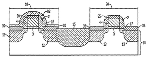
図1を参照すると、本発明の半導体デバイスは、第2のデバイス領域としてのnFETデバイス領域10と第1のデバイス領域としてのpFETデバイス領域20とを含む。分離領域15が、nFETデバイス領域10とpFETデバイス領域20とを分離してもよい。pFETデバイス領域20は、p型ソース/ドレーン領域13を有する少なくとも1つのトランジスタを含む。トランジスタの各々はさらに、ゲート誘電体3の上にゲート導体4を含むゲート領域5を有し、ゲート領域5には側壁スペーサ2が当接する。
Referring to FIG. 1, the semiconductor device of the present invention includes an
低抵抗p型シリサイド・コンタクト35は、p型ソース/ドレーン/ゲート・コンタクト領域13の両方の上に形成され、低抵抗p型シリサイド・コンタクト35の金属は、p型ソース/ドレーン13の材料の価電子帯と実質的に合わせられた仕事関数電位を有する金属シリサイドをもたらすように選択される。p型ソース/ドレーン領域13の上に位置決めされた低抵抗p型シリサイド・コンタクト35は、p型シリサイド・コンタクト35がp型ソース/ドレーン材料13の価電子帯と実質的に合わせられた仕事関数を有する限りは、PtSi、Pt2Si、IrSi、Pd2Si、CoSi2、PdSi、RhSi、YSi、Zr2Si、又は、基板のpFETデバイス領域20のための応力又は接触抵抗について最適化された他のシリサイドとすることができる。低抵抗p型シリサイド・コンタクト35の厚さは、およそ1nmからおよそ40nmまでの範囲とすることができる。
The low resistance p-
nFETデバイス領域10は、n型ソース/ドレーン領域12を有する少なくとも1つのトランジスタを含む。トランジスタの各々はさらに、ゲート誘電体3の上にゲート導体4を含むゲート領域5を有し、ゲート領域5には側壁スペーサ2が当接する。
The
低抵抗n型シリサイド・コンタクト30は、n型ソース/ドレーン/ゲート・コンタクト領域12の両方の上に形成され、低抵抗n型シリサイド・コンタクトの金属は、n型ソース/ドレーン材料12の伝導帯と実質的に合わせられた仕事関数電位を有する金属シリサイドをもたらすように選択される。n型ソース/ドレーン領域12の上に位置決めされた低抵抗n型シリサイド・コンタクト30は、n型シリサイド・コンタクト30がn型ソース/ドレーン材料12の伝導帯と実質的に合わせられた仕事関数を有する限りは、CoSi2、VSi2、ErSi、ZrSi2、HfSi、MoSi2、CrSi2、Zr5Si3、IrSi3、NiSi、又は、基板40のnFETデバイス領域10のための応力又は接触抵抗について最適化された他のシリサイドとすることができる。低抵抗n型シリサイド・コンタクトの厚さは、およそ1nmからおよそ40nmまでの範囲とすることができる。
A low resistance n-
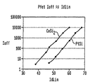
pFETデバイスにp型シリサイド・コンタクトを設ける効果は、図2に描かれたIdlin対Ioffプロットに示されている。Idlinは、デバイスがオンにされたときのpFETデバイスからの出力電流の測定値である。Idlinは、デバイスのオン電流を表し、x軸によって表される。Ioffは、デバイスがオフにされたときのpFETデバイスを通る漏れ電流を表し、y軸によって表される。チャネル長さが減少し、オン電流が増加するのに伴って、漏れ電流が指数関数的に増加する。 The effect of providing a p-type silicide contact in a pFET device is illustrated in the Idlin vs. Ioff plot depicted in FIG. Idlin is a measure of the output current from the pFET device when the device is turned on. Idlin represents the on-current of the device and is represented by the x-axis. Ioff represents the leakage current through the pFET device when the device is turned off and is represented by the y-axis. As the channel length decreases and the on-current increases, the leakage current increases exponentially.
pFETデバイスからの出力電流(Idlin)が増加することにより、デバイスの速度が増大する。出力電流(Idlin)は、シリサイド化プロセスの関数であり得、出力電流は低抵抗シリサイド・コンタクトによって増加し、高抵抗シリサイド・コンタクトによって減少する。デバイスのオフ電流(Ioff)は、ドーパントの位置決め(positioning)の関数であり、シリサイド化プロセスに直接は依存しない。 Increasing the output current (Idlin) from the pFET device increases the speed of the device. The output current (Idlin) may be a function of the silicidation process, with the output current increasing with the low resistance silicide contact and decreasing with the high resistance silicide contact. The device off-current (Ioff) is a function of dopant positioning and does not depend directly on the silicidation process.
したがって、出力電流(Idlin)はシリサイド化プロセスに依存し、オフ電流(Ioff)はシリサイド化プロセスに依存しないため、デバイスへのシリサイド・コンタクトの抵抗の減少は、一定のオフ電流(Ioff)のときの出力電流(Idlin)の増加によって測定することができる。本発明の別の態様は、デバイスからの出力電流(Idlin)を増加させ、オフ電流(Ioff)を一定に保つことによって、デバイスの速度及び性能を向上させることができるという点である。 Therefore, since the output current (Idlin) depends on the silicidation process and the off-current (Ioff) does not depend on the silicidation process, the decrease in resistance of the silicide contact to the device is at a constant off-current (Ioff). Can be measured by increasing the output current (Idlin). Another aspect of the present invention is that the speed and performance of the device can be improved by increasing the output current (Idlin) from the device and keeping the off current (Ioff) constant.
図2を参照すると、CoSi2コンタクト及びPtSiコンタクトのようなシリサイド・コンタクトを有するデバイスのuA/um単位の出力電流(Idlin)が、デバイスのオフ電流(Ioff)に対してプロットされている。図2に描かれたプロットから、CoSi2コンタクトに比べてPtSiコンタクトを用いてpFETデバイスの著しい改善が達成され、y軸上の任意の所与のオフ電流に対して、オン電流(Idlin)は、CoSi2コンタクトからPtSiコンタクトまで増加した。 Referring to FIG. 2, the output current (Idlin) in uA / um for devices having silicide contacts, such as CoSi 2 contacts and PtSi contacts, is plotted against the device off-current (Ioff). From the plot depicted in FIG. 2, a significant improvement of the pFET device is achieved using a PtSi contact compared to a CoSi 2 contact, and for any given off current on the y-axis, the on current (Idlin) is Increased from CoSi 2 contact to PtSi contact.
ここで、図1に描かれたような前述の半導体構造体の形成方法を、図3−図10を参照しながら説明する。本発明の方法の第1の実施形態が、図3−図5に描かれており、pFETデバイス領域20への低抵抗金属シリサイド・コンタクト35と、nFETデバイス領域10への異なる低抵抗金属シリサイド・コンタクト30とを有し、異なるデバイス・タイプのための接触抵抗を改善するようにシリサイドの差異が調整されたCMOS構造体を提供するための、本発明の方法の1つの実施形態が(断面図で)描かれている。
A method of forming the above-described semiconductor structure as depicted in FIG. 1 will now be described with reference to FIGS. A first embodiment of the method of the present invention is depicted in FIGS. 3-5, with a low resistance
図3を参照すると、シリコン(Si)含有材料の基板40上に形成されたnFETデバイス領域10及びpFETデバイス領域20を有する初期状態の構造体が用意される。Si含有材料には、シリコン、単結晶シリコン、多結晶シリコン、シリコン・ゲルマニウム、シリコン−オン−シリコン・ゲルマニウム、アモルファス・シリコン、シリコン−オン−インシュレータ(SOI)、シリコン・ゲルマニウム−オン−インシュレータ(SGOI)、及びアニール化ポリシリコンが含まれるが、これらに限定されるものではない。基板40はさらに、nFETデバイス領域10からpFETデバイス領域20を分離する分離領域15を含む。図3は、pFETデバイス領域20における1つのみのpFETデバイスと、nFETデバイス領域10における1つのみのnFETデバイスとを描いているが、nFETデバイス領域10及びpFETデバイス領域20内の多数のデバイスも意図されており、したがって本発明の開示の範囲内である。
Referring to FIG. 3, an initial structure having an
nFET及びpFETデバイスは、MOSFETデバイスを製造することができる従来の加工ステップを用いることによって形成される。各々のデバイスは、ゲート誘電体3の上にゲート導体4を有するゲート領域5を備える。少なくとも一組の側壁スペーサ2が、ゲート領域5に当接して配置されてもよい。延長領域16、17を含むソース/ドレーン領域12、13が、基板40内に配置され、デバイス・チャネルを画定する。nFETデバイスのソース/ドレーン領域12はn型ドープされる。pFETデバイスのソース/ド
レーン領域13はp型ドープされる。Si含有基板におけるn型ドーパントは、As、Sb及び/又はPのような元素周期表のV族からの元素である。Si含有基板におけるp型ドーパントは、Bのような元素周期表のIII族からの元素である。
nFET and pFET devices are formed by using conventional processing steps that can manufacture MOSFET devices. Each device comprises a
ここで図4を参照すると、ソース/ドレーンのアニール後に、nFETデバイス領域10及びpFETデバイス領域20を含む基板40の上に第1保護層81としてのの窒化物保護層が堆積される。窒化物保護層は、当該技術分野では典型的に知られているように化学気相成長プロセス又は同様のプロセスを用いて堆積される。好ましくは、窒化物保護層は、5nmから約20nmまでの範囲の厚さを有するSi3N4のようなコンフォーマル窒化物である。第1保護層81は窒化物を含むことが好ましいが、代替的に、第1保護層81は、酸化物又は酸窒化物、或いは他の適切な誘電体であってもよい。第1保護層81の材料は、その後のシリサイド化プロセスの間、第1保護層81の一体性が確実に維持されるように選択される。
Referring now to FIG. 4, after the source / drain anneal, a nitride protective layer as a first
次の加工ステップにおいて、第2デバイス領域(pFETデバイス領域20)の上に重なる第1保護層81の部分を保護し、第1デバイス領域(nFETデバイス領域10)の上に重なる第1保護層81の部分を露出する、第1ブロック・マスク50が形成される。次いで、基板40の露出された部分が、適切な金属シリサイドを用いてシリサイド化されて、そこに形成されたデバイスへの低抵抗コンタクトを形成する。図4に描かれた例においては、pFETデバイス領域20(第2デバイス領域)の上に重なり、nFETデバイス領域10(第1デバイス領域)を露出されたまま残して、第1ブロック・マスク50が形成される。この例においては、その後、nFETデバイス領域10内のデバイスへのn型シリサイド・コンタクトが形成される。
In the next processing step, the portion of the first
第1ブロック・マスク50は、低圧化学気相成長(LPCVD)、急速熱処理化学気相成長(RTCVD)、又はプラズマ化学気相成長(PECVD)により、基板40の上にブロック・マスク材料層をブランケット堆積することによって形成され、PECVDを用いるのが好ましい。次いで、従来のフォトリソグラフィ及びエッチング・プロセスを用いてブロック・マスク層がパターン形成される。最初に、構造体全体の上にフォトレジスト層が堆積される。次いで、フォトレジスト層は選択的に露光されて現像され、フォトレジスト層が、基板40のpFETデバイス領域20における第1保護層81の上に重なるブロック・マスク材料層の部分を保護し、nFETデバイス領域10の上に重なる第1保護層81の部分を露出するように、パターン形成される。
The
次に、パターンは、パターン形成されたフォトレジスト又は下にあるnFETデバイス領域10を実質的にエッチングすることなく第1保護層81を選択的に除去するエッチング・プロセスを用いて、第1保護層81に転写される。好ましくは、エッチング・プロセスは、反応性イオン・エッチングのような異方性(directional)エッチングである。
The pattern is then formed using an etching process that selectively removes the first
エッチングの後で、化学ストリップ及び/又は反応性プラズマ・エッチングによってブロック・マスク50が除去される。ブロック・マスク50が除去されると、シリサイド・コンタクトがその後形成される基板40の露出部分の表面をクリーンにするために、クリーニング・プロセスが行われる。クリーニング・プロセスは、当業者には公知の従来の化学クリーニングである。
After etching, the
さらに図4を参照すると、第1シリサイド層30(低抵抗n型シリサイド・コンタクト30)が、nFETデバイス領域10におけるデバイスのソース/ドレーン領域12及びゲート4の上に形成される。シリサイドの形成は、典型的には、Si含有材料の表面上に金属を堆積することを必要とする。図4に描かれた実施形態においては、第1シリサイド層30は低抵抗n型シリサイドであり、第1シリサイド金属は、n型デバイス領域10内のSi含有基板40のn型ソース/ドレーン領域12の伝導帯と実質的に合わせられた仕事関数を有するシリサイドを形成する。Si含有基板40内のn型ドープされたソース/ドレーン領域の伝導帯と実質的に合わせられた仕事関数を有するシリサイドを与えることができる金属としては、とりわけ、Co、Er、V、Zr、Hf、Mo又はCrが挙げられる。シリサイド金属は、めっき及びスパッタリングといった物理堆積法を用いて堆積されることができる。金属層は、約10Åから約100Åまでの範囲の厚さに堆積されることができ、70Åであることが好ましい。
Still referring to FIG. 4, a first silicide layer 30 (low resistance n-type silicide contact 30) is formed over the device source /
堆積の後で、構造体は、これに限定するものではないが急速熱アニーリングのような従来のプロセスを用いるアニーリング・ステップに供される。熱アニーリングの間、堆積された金属は、Siと反応して金属シリサイドを形成する。図4に描かれた実施形態においては、第1シリサイド金属30はCo、Er、V、Zr、Hf、Mo、Ni又はCrを含み、金属シリサイドは、CoSi2、VSi2、ErSi、ZrSi2、HfSi、MoSi2、NiSi、又はCrSi2とすることができる。アニーリング及びクリーニングの詳細は、シリサイドの各々のタイプについて当業者によって最適化されるであろう。CoSi2の場合は、第1アニールは、約1秒から約90秒までの範囲の時間にわたって約350℃から約600℃までの範囲の温度で完了する。本発明の幾つかの実施形態においては、低抵抗n型金属シリサイド・コンタクト30はさらに、随意にTiN層を含んでもよい。
After deposition, the structure is subjected to an annealing step using conventional processes such as, but not limited to, rapid thermal annealing. During thermal annealing, the deposited metal reacts with Si to form a metal silicide. In the embodiment depicted in FIG. 4, the
シリサイド化は、シリサイド金属がSi含有表面の上に堆積されることを必要とする。したがって、シリサイドは、Si含有基板40の露出部分の上に形成されるが、第1ブロック・マスク50又は側壁スペーサ2の上には形成されない。シリサイドは、誘電体材料層でゲート導体をキャッピングすることによって、ゲート導体の上に形成されるのを防止されてもよい。
Silicidation requires that a silicide metal be deposited on the Si-containing surface. Thus, the silicide is formed on the exposed portion of the Si-containing
次いで、側壁スペーサ、分離領域、及び第1ブロック・マスク50の上に位置する未反応シリサイド金属が、ウェット・エッチングを用いて剥離される。好ましくは、未反応の第1シリサイド金属は、未反応シリサイド金属を選択的に除去するウェット・エッチングによって除去される。
The unreacted silicide metal located over the sidewall spacers, isolation regions, and
随意の第2アニールは、低抵抗n型シリサイド・コンタクト30の抵抗率を減少させるために必要とされる。この第2アニールの温度は600℃から800℃までの範囲であり、約1秒から60秒までの範囲の時間にわたる。第2アニールは、CoSi2のようなジシリサイドを形成することができる。CoSi2の厚さは、初めに堆積されたCo金属の厚さの3.49倍である。
An optional second anneal is required to reduce the resistivity of the low resistance n-
シリサイド化の後で、第1保護層81は随意に除去されてもよい。第1保護層81は、pFETデバイス領域又はnFETデバイス領域10、20を実質的にエッチングすることなく第1保護層81を除去する高い選択性を有するウェット・エッチング又はドライ・エッチングによって除去されることができる。
After silicidation, the first
図5を参照すると、次の加工ステップにおいて、第2保護層82が、第1デバイス領域(nFETデバイス領域10)上に形成され、第2デバイス領域(pFETデバイス領域20)は露出されたまま残される。次いで、第2デバイス領域20(pFETデバイス領域)上に第2シリサイド層(低抵抗p型シリサイド・コンタクト35)が形成される。図5に描かれた実施形態においては、nFETデバイス領域10における低抵抗n型シリサイド・コンタクト30の上に重なる第2保護層82が形成され、露出されたpFETデバイス領域20の上に低抵抗p型シリサイド・コンタクト35が形成される。
Referring to FIG. 5, in the next processing step, a second
図4に描かれた第1保護層81を製造するのに用いられるのと同様の材料及びプロセスを用いて、nFETデバイス領域10の上に第2保護層82が形成される。具体的には、第2保護層82は、従来の堆積法、フォトリソグラフィ及びエッチングを用いて形成されることができる。第2保護層82は、酸化シリコン、炭化シリコン、窒化シリコン、又はシリコン炭窒化物、或いは他の適切な誘電体材料を含んでもよく、好ましくは窒化シリコンである。
A second
さらに図5を参照すると、次いで、pFETデバイス領域20の上に第2シリサイド金属が形成され、第2シリサイド金属は、pFETデバイス領域20内の基板40のp型ドープされたソース/ドレーン領域13の価電子帯と実質的に合わせられた仕事関数を有する第2シリサイド層を形成し、これにより低抵抗p型シリサイド・コンタクト35を与える。
Still referring to FIG. 5, a second silicide metal is then formed over the
第2シリサイド金属を堆積する前に、低抵抗p型金属シリサイド・コンタクトがその後形成される表面をクリーンにするために、クリーニング・プロセスが行われる。クリーニング・プロセスは、緩衝化HF又は希釈HFを含むことが好ましい。 Prior to depositing the second silicide metal, a cleaning process is performed to clean the surface on which the low resistance p-type metal silicide contact is subsequently formed. The cleaning process preferably includes buffered HF or diluted HF.
図5に描かれるような低抵抗p型シリサイド・コンタクト35は、p型デバイス領域20上に第2シリサイド金属層を堆積することによって形成され、第2シリサイド金属は、pFET領域20内のSi含有基板40のp型ソース/ドレーン領域13の価電子帯と実質的に合わせられた仕事関数を有するシリサイドを形成する。Si含有基板40のp型ソース/ドレーン領域13の価電子帯と実質的に合わせられた仕事関数を有するシリサイドを与えることができる金属には、Pt、Ir、Pd、並びに、pFETデバイスの価電子帯と実質的に合わせられた仕事関数を有する他の金属がある。p型シリサイド金属は、めっき及びスパッタリングといった物理堆積法を用いて堆積されることができる。第2シリサイド金属層は、1nmから約10nmまでの範囲の厚さに堆積されることができる。
A low resistance p-
堆積後に、構造体は、これに限られるものではないが急速熱アニーリングのような従来のプロセスを用いるアニーリング・ステップに供される。熱アニーリングの間に、堆積された第2シリサイド金属がSiと反応してPtSi、Pt2Si、IrSi、Pd2Siといった金属シリサイドを形成する。アニーリング及びクリーニング条件は、シリサイドによって変化することになり、当業者には公知である。PtSiの場合、第1アニールは、約1秒から約90秒までの範囲の時間にわたって350℃から600℃までの範囲の温度で完了する。Pt−シリサイドの厚さは、堆積されたシリサイド金属の厚さの1.98倍である。 After deposition, the structure is subjected to an annealing step using conventional processes such as but not limited to rapid thermal annealing. During thermal annealing, the deposited second silicide metal reacts with Si to form a metal silicide such as PtSi, Pt 2 Si, IrSi, Pd 2 Si. Annealing and cleaning conditions will vary with the silicide and are known to those skilled in the art. For PtSi, the first anneal is completed at a temperature in the range of 350 ° C. to 600 ° C. for a time in the range of about 1 second to about 90 seconds. The thickness of the Pt-silicide is 1.98 times the thickness of the deposited silicide metal.
側壁スペーサ2、分離領域15、及び第2保護層82の上に位置する未反応の第2シリサイド金属が、ウェット・エッチングを用いて剥離される。好ましくは、未反応Ptは、硝酸及びHClを含むウェット・エッチングを用いて除去される。次の加工ステップにおいて、第2保護層82は、nFETデバイス領域10又はpFETデバイス領域20を実質的にエッチングすることなく第2保護層82を除去する高い選択性を有するウェット・エッチング又はドライ・エッチングによって除去されることができる。
The unreacted second silicide metal located on the
シリサイドの形成後に、基板40は、従来のバック・エンド・オブ・ライン(BEOL)プロセスを用いて加工されてもよい。例えば、誘電体材料層を基板全体の上にブランケット堆積し、平坦化し、その中に、低抵抗n型及びp型シリサイド・コンタクト30、35への相互接続部を形成することができる。
After the formation of the silicide, the
ブランケット誘電体は、SiO2、Si3N4、SiOxNy、SiC、SiCO、SiCOH、及びSiCH化合物といったシリコン含有材料、幾らか又は全てのSiがGeによって置換された前述のシリコン含有材料、炭素ドープ酸化物、ホウ素及びリンドープ酸化物、無機酸化物、無機ポリマー、ハイブリッド・ポリマー、ポリアミド又はSiLK(商標)のような有機ポリマー、他の炭素含有材料、スピン−オン・ガラス及びシルセスキオキサンベースの材料のような有機−無機材料、並びにダイヤモンド状炭素(DLC、アモルファス水素化炭素、a−C:H)からなる群から選択されることができる。 The blanket dielectric is a silicon-containing material such as SiO 2 , Si 3 N 4 , SiO x N y , SiC, SiCO, SiCOH, and SiCH compound, the silicon-containing material described above, where some or all of the Si is replaced by Ge, Carbon doped oxides, boron and phosphorus doped oxides, inorganic oxides, inorganic polymers, hybrid polymers, organic polymers such as polyamides or SiLK ™, other carbon-containing materials, spin-on glasses and silsesquioxanes It can be selected from the group consisting of organic-inorganic materials such as base materials, as well as diamond-like carbon (DLC, amorphous hydrogenated carbon, a-C: H).
従来のフォトリソグラフィ及びエッチングを用いて誘電体材料内にバイアが形成され、従来のプロセスを用いてバイア・ホールの中に導電性金属を堆積することによって、低抵抗n型及びp型シリサイド・コンタクト30、35への相互接続部がバイアの中に形成される。 Low resistance n-type and p-type silicide contacts are formed by forming vias in the dielectric material using conventional photolithography and etching and depositing conductive metal into the via holes using conventional processes. Interconnections to 30, 35 are formed in the vias.
図3−図5には描かれていないが、もう1つの方法として、nFETデバイス領域を保護し、pFETデバイス領域を露出されたまま残す第1保護層が形成されてもよく、その後、pFETデバイス領域内に位置するデバイス・コンタクトへの低抵抗p型シリサイドが形成される。nFETデバイス領域から第1保護層を除去した後で、pFETデバイス領域における低抵抗p型金属シリサイドの上に重なる第2保護層が形成され、露出されたnFETデバイス領域の上に低抵抗n型金属シリサイド層が形成される。 Although not depicted in FIGS. 3-5, as an alternative, a first protective layer may be formed that protects the nFET device region and leaves the pFET device region exposed, after which the pFET device is formed. A low resistance p-type silicide is formed to the device contact located in the region. After removing the first protective layer from the nFET device region, a second protective layer is formed overlying the low resistance p-type metal silicide in the pFET device region, and the low resistance n-type metal over the exposed nFET device region. A silicide layer is formed.
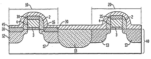
図6−図7は、pFETデバイス領域への低抵抗金属シリサイド・コンタクトと、nFETデバイス領域への異なる低抵抗金属シリサイド・コンタクトとを有し、異なるデバイス・タイプについての接触抵抗を改善するようにシリサイドの差異が調整されたCMOS構造体を提供するための、本発明の方法の第2の実施形態を(断面図で)示す。図6−図7を参照すると、nFETデバイス領域10への低抵抗n型シリサイド・コンタクト30と、pFETデバイス領域20への低抵抗p型シリサイド・コンタクト35とを有するCMOS構造体を提供するための加工ステップの数は、1つ又は複数のブロック・マスク及び保護層の使用を排除することによって減らされる。例えば、本発明の第1の実施形態において用いられる第2保護層を排除し、第1デバイス領域(n型デバイス領域)における第1シリサイド層(低抵抗n型シリサイド・コンタクト)の上、及び第2デバイス領域(p型デバイス領域)における基板表面の上に第2金属層ブランケット45を堆積することができる。ここで、本発明の第2の実施形態をより詳しく説明する。
6-7 have low resistance metal silicide contacts to pFET device regions and different low resistance metal silicide contacts to nFET device regions to improve contact resistance for different device types. Figure 2 shows (in cross-section) a second embodiment of the method of the present invention to provide a CMOS structure with tailored silicide differences. 6-7, a CMOS structure having a low resistance n-
第1の実施形態の図3−図4に描かれた最初の加工ステップと同様に、第1シリサイド層30(低抵抗n型シリサイド・コンタクト30)が、堆積、フォトリソグラフィ、及びエッチング・プロセスを用いて第1デバイス領域10(n型デバイス領域10)の上に選択的に形成される。具体的には、第1保護層81が、nFETデバイス領域10を露出されたまま残して、基板40の一部の上に形成される。次いで、第1シリサイド金属の金属層がnFETデバイス領域の上に堆積され、これがその後のアニーリングの間に低抵抗n型シリサイド・コンタクトを形成する。第1シリサイド金属は、好ましくは、CoSi2、VSi2、ErSi、ZrSi2、HfSi、MoSi2、CrSi2、並びに、nFETデバイスの伝導帯と実質的に合わせられた仕事関数を有する他のものを含み、基板40のnFETデバイス領域10におけるn型ソース/ドレーン領域12の伝導帯と実質的に合わせられた仕事関数を有するシリサイドをもたらす。
Similar to the first processing steps depicted in FIGS. 3-4 of the first embodiment, a first silicide layer 30 (low resistance n-type silicide contact 30) is used for deposition, photolithography, and etching processes. And selectively formed on the first device region 10 (n-type device region 10). Specifically, a first
図6を参照すると、本発明の第2の実施形態においては、低抵抗n型シリサイド・コンタクト30の形成後に、第1保護層81が基板40から除去され、nFETデバイス領域10における低抵抗n型シリサイド・コンタクト30及びpFETデバイス領域20の基板40の表面上に第2金属ブランケット層45が直接堆積される。第1保護層81は、形成されたn型シリサイド・コンタクト30又はp型デバイス領域20の表面を実質的にエッチングすることなく第1ブロック・マスクを除去する高選択性エッチング・プロセスによって除去される。
Referring to FIG. 6, in the second embodiment of the present invention, after the formation of the low resistance n-
第1保護層81の除去後に、低抵抗n型シリサイド・コンタクト30及びp型デバイス領域20の表面が、シリサイド化のためのクリーンな表面を与えるためにクリーニングされる。クリーニング・プロセスは、当業者には公知の従来の化学クリーニングとすることができる。
After removal of the first
次に、第2金属ブランケット層45がpFETデバイス領域20及び低抵抗n型シリサイド・コンタクト30の上に直接堆積される。第2金属ブランケット層45は、基板40のpFETデバイス領域20内のp型ソース/ドレーン領域13の価電子帯と実質的に合わせられた仕事関数を有するシリサイドをその後に形成する第2シリサイド金属を含む。第2金属ブランケット層45は、スパッタリング及びめっきといった物理気相成長法を用いて堆積されることができ、約1nmから約10nmまでの範囲の厚さを有する。第2金属ブランケット層45は、好ましくは、Pt、Ir、Pd、並びに、pFETデバイスの価電子帯と実質的に合わせられた仕事関数を有する他のものを含む。
Next, a second metal blanket layer 45 is deposited directly over the
図7を参照すると、第2金属ブランケット層45は次にアニーリングされて、基板40のpFETデバイス領域20内のp型ソース/ドレーン領域13の価電子帯と実質的に合わせられた仕事関数を有する第2シリサイド層35をもたらし、それにより低抵抗p型シリサイド・コンタクト35を与える。アニーリングの間に、第2金属ブランケット層45は、nFETデバイス領域10内の低抵抗n型金属コンタクト30と混合されて、Co、V、Er、Zr、Hf、Mo、Ni、Cr、並びに、nFETデバイスの伝導帯と実質的に合わせられた仕事関数を有する他のものを含むことができる低抵抗n型金属シリサイド・コンタクト30’を形成する。
Referring to FIG. 7, the second metal blanket layer 45 is then annealed to have a work function substantially aligned with the valence band of the p-type source /
Ptを取り込むことは、低抵抗n型シリサイド・コンタクト30’の仕事関数を、バンド・ギャップの中央の方、且つn型ソース/ドレーン領域12の伝導帯から遠ざかる方へ配置する。しかしながら、Ptを低抵抗n型金属コンタクト30の中に混合するにもかかわらず、低抵抗n型シリサイド・コンタクト30’の仕事関数は、依然としてn型ソース/ドレーン領域12の伝導帯と実質的に合わせられ、10−9ohm・cm−2から10−7ohm・cm−2までの範囲の接触抵抗を有するコンタクトを与える。
Incorporating Pt places the work function of the low resistance n-
シリサイド化の後で、第2金属ブランケット層45の未反応部分が、nFETデバイス領域10及びpFETデバイス領域20内の構造体を実質的にエッチングしない選択的エッチングによって除去される。好ましくは、未反応Ptは、硝酸及びHClを含む化学ストリップを用いて除去される。
After silicidation, unreacted portions of the second metal blanket layer 45 are removed by selective etching that does not substantially etch the structures in the
図3−図5に描かれた実施形態と同様に、nFETデバイス領域を保護し、pFETデバイス領域を露出されたまま残す第1保護層が代替的に形成されてもよく、その後、Ptを含む低抵抗p型シリサイド・コンタクトがpFETデバイス領域10内に形成されたデバイスに対して形成される。nFETデバイス領域から第1保護層を除去した後で、Co、V、Er、Zr、Hf、Mo、Ni、Crを含む第2金属層が、低抵抗p型シリサイド・コンタクト及び露出されたnFETデバイス領域の上に形成され、nFETデバイス領域内に形成されたデバイスへの低抵抗n型シリサイド・コンタクトが形成され、アニーリングの間に第2金属層が低抵抗p型金属シリサイド・コンタクトと混合される。
Similar to the embodiment depicted in FIGS. 3-5, a first protective layer may be alternatively formed that protects the nFET device region and leaves the pFET device region exposed, and then includes Pt. A low resistance p-type silicide contact is formed for the device formed in the
Co、V、Er、Zr、Hf、Mo、Ni、又はCrが低抵抗p型シリサイド・コンタクト30の中に取り込まれるにもかかわらず、低抵抗p型シリサイド・コンタクトの仕事関数は、依然としてp型ソース/ドレーン領域13の価電子帯と実質的に合わせられ、10−9ohm・cm−2から10−7ohm・cm−2までの範囲の低い接触抵抗を有するコンタクトを与える。
Despite the incorporation of Co, V, Er, Zr, Hf, Mo, Ni, or Cr into the low resistance p-
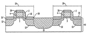
図8−図10は、pFETデバイス領域への低抵抗金属シリサイド・コンタクトと、nFETデバイス領域への異なる低抵抗金属シリサイド・コンタクトとを有し、異なるデバイス・タイプについての接触抵抗を改善するようにシリサイドの差異が調整されたCMOS構造体を提供するための、本発明の方法の第3の実施形態を(断面図で)示す。図8−図10を参照すると、本発明の第3の実施形態においては、nFETデバイス領域10への低接触抵抗n型シリサイド・コンタクト30と、pFETデバイス領域20への低抵抗p型シリサイド・コンタクト35とを有するCMOS構造体を提供するための加工ステップの数は、nFETデバイス領域10及びpFETデバイス領域20を含む基板40の上に第1金属層(第1金属ブランケット層)60を直接ブランケット堆積することによってさらに減らされる。ここで、本発明の第3実施形態をより詳しく説明する。
8-10 have a low resistance metal silicide contact to the pFET device region and a different low resistance metal silicide contact to the nFET device region to improve contact resistance for different device types. Figure 3 shows (in cross-section) a third embodiment of the method of the invention for providing a CMOS structure with tailored silicide differences. Referring to FIGS. 8-10, in a third embodiment of the present invention, a low contact resistance n-
図8を参照すると、第1加工ステップにおいて、nFETデバイス領域10及びpFETデバイス領域20を含む基板40の表面全体の上に第1金属層60が直接ブランケット堆積される。堆積前に、基板40の表面は、緩衝化HF、希釈HF、水酸化アンモニウム−過酸化水素、及び/又は、塩酸−過酸化水素を含む化学クリーニング組成物を用いてクリーニングされる。
Referring to FIG. 8, in a first processing step, a
その後、第1金属層60は、低抵抗n型シリサイド又は低抵抗p型シリサイドのいずれかを与える。低抵抗n型金属シリサイドは、シリサイド化されたときにnFETデバイス領域10における基板40のn型ドープされたソース/ドレーン領域12の伝導帯と実質的に合わせられた仕事関数を与えるCo、V、Er、Zr、Hf、Mo、Ni、Crといったシリサイド金属を堆積することによって形成される。p型金属シリサイドは、シリサイド化されたときにpFETデバイス領域20における基板40のp型ドープされたソース/ドレーン領域13の価電子帯と実質的に合わせられた仕事関数を与える金属、Pt、Ir又はPdを堆積することによって形成される。第1金属層60は、めっき及びスパッタリングといった物理堆積法を用いて堆積されることができる。図8−図10に描かれた実施形態においては、第1金属層60は、Co、V、Er、Zr、Hf、Mo、Ni、又はCrを含む。
Thereafter, the
図9を参照すると、堆積後に、第1金属層60は、アニーリングされて、nFETデバイス領域10への低抵抗n型金属シリサイド・コンタクト30を与える。本発明の第1実施形態と同様に、第1金属層60は、急速熱アニーリングのような従来のアニーリング・プロセスを用いて、350℃から600℃の範囲の温度で1秒から90秒の範囲の時間にわたりアニールされる。このシリサイド化プロセスの間に、pFETデバイス領域20の上に堆積された第1金属層60が、Co、V、Er、Zr、Hf、Mo、又はCrを含むpFETデバイス領域20における初期のシリサイド65を形成する。シリサイド化の後で、nFETデバイス領域10、pFETデバイス領域20又は基板40を実質的にエッチングすることなく残りの未反応の第1金属層60を除去する選択性を有するウェット・エッチングによって、残りの未反応の第1金属層60が除去される。
Referring to FIG. 9, after deposition, the
さらに図9を参照すると、第1保護層81が、pFETデバイス領域20を露出されたまま残して、nFETデバイス領域10の上に形成される。前の実施形態と同様に、第1保護層81は、好ましくは、窒化シリコンを含み、図4を参照しながら前述されたように、堆積、フォトリソグラフィ及びエッチングを用いて形成される。次いで、pFETデバイス領域20の表面が、シリサイド化のためのpFETデバイス領域20を用意するために、化学クリーニングを用いてクリーニングされる。このクリーニング・プロセスは、初期シリサイド65がpFETデバイス領域20に存在するため、省略されてもよい。
Still referring to FIG. 9, a first
次に、第2金属層(第2金属ブランケット層)70が、nFETデバイス領域10における第1保護層81を含む基板40の全体の上、及びpFETデバイス領域20における初期シリサイド65の上にブランケット堆積される。図8−図10に描かれた実施形態においては、第2金属層70は、基板40のpFET領域20におけるp型ソース/ドレーン領域13の荷電子帯と実質的に合わせられた仕事関数を有するシリサイドをもたらす、Pt、Ir又はPdといった金属を含む。
Next, a second metal layer (second metal blanket layer) 70 is blanket deposited over the
堆積後に、第2金属層70がアニーリングされ、アニーリングの間に、第2金属層70が初期シリサイド65と混合されて、pFETデバイス領域20への低抵抗p型シリサイド・コンタクト35’を形成する。低抵抗p型シリサイド35’コンタクトは、Co、V、Er、Zr、Hf、Mo、Ni又はCrと組み合わせてPt、Ir又はPdを含む。Pt、Ir又はPdの取り込みは、初期シリサイド・コンタクト65の仕事関数を、p型ソース/ドレーン領域13の価電子帯の方へと配置し、低抵抗p型シリサイド・コンタクト35をもたらす。Co、V、Er、Zr、Hf、Mo、Ni又はCrがPt、Ir又はPd−シリサイドに取り込まれるにもかかわらず、低抵抗p型シリサイド・コンタクト35の仕事関数は、p型ソース/ドレーン領域13の価電子帯と実質的に合わせられ、10−9ohm・cm−2から10−7ohm・cm−2までの範囲の低い接触抵抗を有するコンタクトを与える。
After deposition, the
nFETデバイス領域10は第1保護層81によって保護され、シリサイド化はSi含有表面を必要とするため、シリサイドはnFETデバイス領域10の上に形成されない。シリサイド化の後で、10に描かれるように、第2金属層70の未反応部分及び第1保護層81が、nFETデバイス領域10及びpFETデバイス領域内の構造体を実質的にエッチングしない選択的エッチングを用いて除去される。
Since the
図8−図10に描かれた実施形態においては、第1金属層は、代替的に、nFETデバイス領域及びpFETデバイス領域の上に直接堆積されるPt、Ir又はPdといった低抵抗p型シリサイド・コンタクトを与える金属を含んでもよく、次いで、第1金属層は、アニーリングされて、pFETデバイス領域への低抵抗p型金属シリサイド・コンタクト及びnFETデバイス領域への初期シリサイドを与え、nFETデバイス領域への初期シリサイドはPt、Ir又はPdを含む。次いで、第1保護層が、nFETデバイス領域を露出されたまま残して、pFETデバイス領域の上に形成される。次いで、Co、V、Er、Zr、Hf、Mo、Ni又はCrを含む第2金属層を、初期シリサイドを含む露出されたnFETデバイス領域の上に形成することができ、アニーリングの間に、第2金属層と初期シリサイドが混合されて、n型デバイス領域への低抵抗n型金属シリサイド・コンタクトを与える。 In the embodiment depicted in FIGS. 8-10, the first metal layer is alternatively a low resistance p-type silicide, such as Pt, Ir, or Pd, deposited directly over the nFET and pFET device regions. The first metal layer may then be annealed to provide a low resistance p-type metal silicide contact to the pFET device region and an initial silicide to the nFET device region, and the first metal layer may be annealed. The initial silicide includes Pt, Ir, or Pd. A first protective layer is then formed over the pFET device region, leaving the nFET device region exposed. A second metal layer comprising Co, V, Er, Zr, Hf, Mo, Ni or Cr can then be formed over the exposed nFET device region comprising the initial silicide, and during annealing, The two metal layers and the initial silicide are mixed to provide a low resistance n-type metal silicide contact to the n-type device region.
PtSi、Pt2Si、IrSi、Pd2Si、並びに、pFETデバイスの価電子帯と実質的に合わせられた仕事関数を有する他のもの。第1型シリサイド・コンタクトは、CoSi2、VSi2、ErSi、ZrSi2、HfSi、MoSi2、NiSi、CrSi2、並びに、nFETデバイスの伝導帯と実質的に合わせられた仕事関数を有する他のものを含むことができる。
PtSi, Pt 2 Si, IrSi, Pd 2 Si, and others with work functions substantially aligned with the valence band of the pFET device.
Co、V、Er、Zr、Hf、Mo、Ni又はCrの取り込みは、初期シリサイド・コンタクトの仕事関数をn型ソース/ドレーン領域の伝導帯の方へ配置し、低抵抗n型金属リサイド・コンタクトをもたらす。Pt、Ir又はPdがCo、V、Er、Zr、Hf、Mo、Ni又はCrシリサイドに取り込まれるにもかかわらず、低抵抗n型金属シリサイド・コンタクトの仕事関数は、n型ソース/ドレーン領域の伝導帯と実質的に合わせられ、10−9ohm・cm−2から10−7ohm・cm−2までの範囲の低い接触抵抗を有するコンタクトを与える。 The incorporation of Co, V, Er, Zr, Hf, Mo, Ni or Cr places the work function of the initial silicide contact towards the conduction band of the n-type source / drain region, resulting in a low resistance n-type metal resided contact Bring. Despite the incorporation of Pt, Ir or Pd into Co, V, Er, Zr, Hf, Mo, Ni or Cr silicide, the work function of the low resistance n-type metal silicide contact is that of the n-type source / drain region. A contact that is substantially matched to the conduction band and has a low contact resistance ranging from 10 −9 ohm · cm −2 to 10 −7 ohm · cm −2 .
本発明の別の実施形態においては、nFETデバイス領域及びpFETデバイス領域に形成されたシリサイド化金属は、pFETデバイス及びnFETデバイスにおけるキャリア移動度を増加させることによって、歪みに基づくデバイスの改善を与えるように選択されることができる。 In another embodiment of the present invention, the silicided metal formed in the nFET and pFET device regions provides improved device based on strain by increasing the carrier mobility in the pFET and nFET devices. Can be selected.
好ましい実施形態においては、pFET領域及びnFET領域を有する基板を含む半導体デバイスが提供され、nFET領域内のデバイスへのシリサイド・コンタクトはnFETデバイス性能を増加させる応力場をもたらし、pFET領域内のデバイスへのシリサイド・コンタクトはpFETデバイス性能を増加させるpFET領域内の応力場をもたらし、pFET領域内の応力場はnFET領域内の応力場よりも圧縮性が高い。 In a preferred embodiment, a semiconductor device is provided that includes a substrate having a pFET region and an nFET region, wherein the silicide contact to the device in the nFET region provides a stress field that increases nFET device performance, and to the device in the pFET region. The silicide contact provides a stress field in the pFET region that increases pFET device performance, and the stress field in the pFET region is more compressible than the stress field in the nFET region.
キャリア移動度は、pFETデバイスが形成される基板において圧縮応力場を生じさせることによって、pFETデバイスにおいて増大することができる。キャリア移動度は、pFET領域よりも低い圧縮応力をnFET領域内に生じさせることによって、又は、nFET領域において引張応力を形成することによって、nFETデバイスにおいて増大することができる。 Carrier mobility can be increased in pFET devices by creating a compressive stress field in the substrate on which the pFET device is formed. Carrier mobility can be increased in nFET devices by creating a lower compressive stress in the nFET region than in the pFET region, or by creating a tensile stress in the nFET region.
基板のnFET領域及びpFET領域の選択的処理は、前述の方法のいずれかを用いて達成され、接触抵抗を最適化する目的のためにプロセス条件及びシリサイド金属組成を選択する代わりに、プロセス条件及びシリサイド金属組成は、歪みに基づくデバイスの改善を与えるように選択される。 Selective processing of the nFET and pFET regions of the substrate is accomplished using any of the methods described above, instead of selecting process conditions and silicide metal composition for the purpose of optimizing contact resistance. The silicide metal composition is selected to provide device improvements based on strain.
1つの例において、nFET領域上にコバルトを堆積し、基板のpFET領域上にコバルト・シリコン合金を堆積することによって応力差が与えられ、シリサイド化の後で、コバルト・ジシリサイド・コンタクトがpFETデバイス及びnFETデバイス上に形成される。ここで、nFETデバイス領域とpFETデバイス領域との間の応力差を有する半導体デバイスを形成するための方法を、図11を参照しながらより詳しく説明する。 In one example, a stress difference is provided by depositing cobalt on the nFET region and depositing a cobalt silicon alloy on the pFET region of the substrate, and after silicidation, the cobalt disilicide contact is connected to the pFET device and Formed on nFET devices. A method for forming a semiconductor device having a stress difference between an nFET device region and a pFET device region will now be described in more detail with reference to FIG.
図3−図5に描かれた実施形態と同様に、nFETデバイス領域10及びpFETデバイス領域20を含む基板40が与えられる。次いで、第1保護層81が、第1デバイス領域、すなわちnFETデバイス領域10を露出されたまま残して、第2デバイス領域20、すなわちpFETデバイス領域20の上に形成される。
Similar to the embodiment depicted in FIGS. 3-5, a
次いで、露出されたデバイス領域は、基板内に応力場を誘起するデバイス・シリサイド・コンタクトを与えるように処理され、その上に形成されたデバイスに歪みに基づくデバイスの改善をもたらす。例えば、コバルトは、nFETデバイスにおいて歪みに基づくデバイスの改善のための適切な応力場を生み出す金属シリサイド・コンタクトを与えるために、nFETデバイス領域のシリコン含有表面の上に堆積される。堆積後に、コバルト金属は、アニーリングされて、nFETデバイス領域のシリコン表面の上に堆積されたコバルトはnFET金属シリサイド・コンタクト30’に変換される。コバルトのシリサイド化の間に生み出された応力状態は、nFET金属シリサイド・コンタクト30’に隣接するシリコン含有基板の部分の中に低圧縮性応力から引張応力までの状態を与えることができる。シリサイド化の後で、コバルトの未反応部分が選択的エッチング・プロセスによって除去される。応力は、反応したシリコンに対する生じたシリサイドの体積の変化に起因すると考えられる。CoSi2の場合には、シリサイドの体積は、反応したシリコンよりも3%小さく、これは、nFETにおけるキャリアの移動度のために望ましいものとなる中程度の引張応力を生み出すと考えられる。それに対して、CoSi2に変換されるCo2Siは、基板の反応したシリコンよりも29%大きいシリサイド体積を有し、これは、pFETにおけるキャリア移動度を改善する圧縮応力をもたらすことになる。 The exposed device region is then processed to provide a device silicide contact that induces a stress field in the substrate, resulting in a device improvement based on strain on the device formed thereon. For example, cobalt is deposited on the silicon-containing surface of the nFET device region to provide a metal silicide contact that creates an appropriate stress field for strain-based device improvement in nFET devices. After deposition, the cobalt metal is annealed and the cobalt deposited on the silicon surface of the nFET device region is converted to an nFET metal silicide contact 30 '. The stress conditions created during the silicidation of cobalt can give conditions from low compressive stress to tensile stress in the portion of the silicon-containing substrate adjacent to the nFET metal silicide contact 30 '. After silicidation, the unreacted portion of cobalt is removed by a selective etching process. The stress is believed to be due to the resulting change in silicide volume relative to the reacted silicon. In the case of CoSi 2 , the volume of silicide is 3% smaller than the reacted silicon, which is thought to produce moderate tensile stresses that are desirable for carrier mobility in nFETs. In contrast, Co 2 Si that is converted to CoSi 2 has a silicide volume that is 29% greater than the reacted silicon of the substrate, which will result in compressive stress that improves carrier mobility in the pFET.
ここで図12を参照すると、次の一連の加工ステップにおいて、第2保護層82が、基板40のpFET領域を露出されたまま残してnFETデバイス領域10の上に形成される。次いで、基板40のpFET領域20は、基板40内に応力場を誘起するpFET金属シリサイド・コンタクト35’を与えるように処理され、これがpFETデバイスにおいて歪みに基づくデバイスの改善をもたらす。1つの例において、コバルト・シリサイド合金(例えばCo2Si)が、基板40のpFET領域20の露出されたSi含有表面上に堆積され、コバルト・シリコン合金のシリサイド化の間に生じた応力状態は、pFET金属シリサイド・コンタクト35’に隣接する基板40の部分の中に高圧縮性の応力状態を与えることができる。
Referring now to FIG. 12, in the next series of processing steps, a second
コバルト・シリコン合金金属は、5原子量%から25原子量%までのシリコンと、95原子量%から75原子量%までのコバルトとを含む。好ましい実施形態においては、コバルト・シリコン合金はCo2Siである。コバルト・シリサイド合金と基板40との間のエッチング選択性が維持され、シリサイド化プロセスの間、基板40のpFET領域20内に圧縮応力が生み出される限り、他のシリコン濃度もまた意図されることに注意されたい。堆積後に、300℃から450℃までの範囲内の低温アニールが、Siに接触する領域において、材料をよりシリコン・リッチなシリサイドに変換する。この、よりシリコンリッチなシリサイドではなくCo2Siを除去するために選択的エッチングが用いられ、600℃から800℃までのさらなるアニールが、pFETシリサイド・コンタクト35’についてCoSi2への変換を完了させる。
Cobalt-silicon alloy metals include from 5 atomic percent to 25 atomic percent silicon and from 95 atomic percent to 75 atomic percent cobalt. In a preferred embodiment, the cobalt silicon alloy is Co 2 Si. Other silicon concentrations are also contemplated as long as the etch selectivity between the cobalt silicide alloy and the
基板のnFETデバイス領域10とpFETデバイス領域20との間の応力差は、基板40のpFET領域20において堆積されたコバルト・シリコン合金にSiが取り込まれることに起因する。本発明においては、Siを含有するコバルト合金層を堆積することにより、シリコン含有基板からコバルト合金層のシリサイドに要求されるシリコンの量を減少させる。コバルト合金のシリサイド化の間に基板のシリコン格子から除去されるシリコンをより少なくすることによって、その後形成されるpFET金属シリサイド・コンタクトに隣接する圧縮歪みの増大をもたらす体積膨張が起こる。既に述べたように、形成されたCoSi2と基板からの反応したシリコンとの間の体積差は、反応後では29%大きい体積である。これは、pFETキャリア移動度を助ける圧縮応力を生み出すことになる。
The stress difference between the
本発明の別の実施形態においては、基板40のpFETデバイス領域20は、白金シリサイドを与えるように処理されることができる。本発明のこの実施形態においては、pFETデバイス領域20とnFETデバイス領域10との間の応力差は、基板40のnFETデバイス領域10にコバルト・シリサイド又はコバルト・ジシリサイド・コンタクトを形成し、pFETデバイス領域に白金及びコバルトを含有するシリサイドを形成することによって生じる。基板のnFETデバイス領域におけるコバルト・シリサイド又はコバルト・ジシリサイドは、nFET領域10内に低圧縮又は引張応力場を生み出し、それにより、nFETデバイスにおけるキャリア移動度及びデバイス性能を向上させる。白金及びコバルトを含有するシリサイドは、pFETデバイス領域内に圧縮応力場を生み出し、それにより、pFETデバイスにおけるキャリア移動度及びデバイス性能を向上させる。
In another embodiment of the present invention, the
これらは、pFET内の応力を最適化するための材料の2つの例にすぎない。各々のデバイス内の応力を最適化させるシリサイドの例を挙げる。例えば、CoSi2は、消費されたシリコンに対するシリサイドの体積比0.97を有し、これは、中程度の引張応力を生み出し、nFETの移動度に有利となる。PtSiは、消費されたシリコンに対するシリサイドの体積比1.5を有し、これは、圧縮応力を生み出し、pFETの移動度に有利となる。nFETにおける移動度に有利な、消費されたシリコンに対するシリサイドの体積比を有するシリサイドのさらなる例は、0.9の比をもつCrSi2、0.9の比をもつIrSi3、0.87の比をもつMoSi2であり、他のシリサイドもこの基準を満たすであろう。pFETにおける移動度に有利な、消費されたシリコンに対するシリサイドの体積比を有するシリサイドのさらなる例は、1.45の比をもつPdSi、1.35の比をもつRhSi、及び、2.13の比をもつYSiであり、他のシリサイドもこの基準を満たすであろう。 These are just two examples of materials for optimizing stress in the pFET. Take an example of a silicide that optimizes the stress in each device. For example, CoSi 2 has a volume ratio of silicide to silicon consumed of 0.97, which produces moderate tensile stress and favors nFET mobility. PtSi has a volume ratio of silicide to silicon consumed of 1.5, which creates compressive stress and favors pFET mobility. A further example of a silicide having a volume ratio of silicide to consumed silicon that favors mobility in nFETs is CrSi 2 with a ratio of 0.9, IrSi 3 with a ratio of 0.9, ratio of 0.87 a MoSi 2 with, other silicides will also meet this criterion. Further examples of silicides with a volume ratio of silicide to consumed silicon favoring mobility in pFETs are PdSi with a ratio of 1.45, RhSi with a ratio of 1.35, and a ratio of 2.13. And other silicides will meet this criterion.
この応力差を生み出すための別の方法は、同じベース金属から2相のシリサイドをもたらすことであり、例えば、Zr2Siは2.7の比を有し、pFETに有利であり、Zr5Si3は0.25の比を有し、nFETに有利である。 Another way to create this stress difference is to provide a two-phase silicide from the same base metal, for example, Zr 2 Si has a ratio of 2.7, which is advantageous for pFETs, Zr 5 Si 3 has a ratio of 0.25, which is advantageous for nFETs.
この応力差を生み出すためのさらに別の方法は、nFET上にCoを堆積して0.97の比をもつCoSi2を形成し、そして5%から25%のシリコンを含有するCo合金を堆積することであり、これは、例えばCo2Siを堆積して、pFETに有利な応力を生み出すことになる約1.29の比を有するCoSi2を形成することである。 Yet another way to create this stress difference is to deposit Co on the nFET to form CoSi 2 with a ratio of 0.97 and to deposit a Co alloy containing 5% to 25% silicon. This is to deposit, for example, Co 2 Si to form CoSi 2 having a ratio of about 1.29 that will create stresses favorable to the pFET.
本発明を、その好ましい実施形態に関して特定的に図示され説明してきたが、形態及び詳細における上記の及び他の変化は、本発明の精神及び範囲から逸脱することなく成され得ることを、当業者であれば理解するであろう。したがって、本発明は、説明され図示された正確な形態及び詳細に限定されるものではなく、添付の請求項の範囲内に含まれることが意図される。 While the invention has been particularly shown and described with respect to preferred embodiments thereof, those skilled in the art will recognize that these and other changes in form and detail may be made without departing from the spirit and scope of the invention. You will understand. Accordingly, the invention is not limited to the precise forms and details described and illustrated, but is intended to be included within the scope of the following claims.
2:側壁スペーサ
3:ゲート誘電体
4:ゲート導体
5:ゲート領域
10:nFETデバイス領域
12、13:ソース/ドレーン領域
15:分離領域
20:pFETデバイス領域
30、35:シリサイド・コンタクト
30‘、35’:シリサイド・コンタクト
40:基板
45、60:金属層
50:ブロック・マスク
81、82:保護層
2: Side wall spacer 3: Gate dielectric 4: Gate conductor 5: Gate region 10:
Claims (28)
第1デバイス領域におけるp型デバイス及び第2デバイス領域におけるn型デバイスを有する基板と、
前記第2デバイス領域における前記n型デバイスへの第1型シリサイド・コンタクトであって、前記第2デバイス領域における前記n型デバイスの伝導帯と実質的に合わせられた仕事関数を有する第1型シリサイド・コンタクトと、
前記第1デバイス領域における前記p型デバイスへの第2型シリサイド・コンタクトであって、前記第1デバイス領域における前記p型デバイスの価電子帯と実質的に合わせられた仕事関数を有する第2型シリサイド・コンタクトと、
を備える半導体構造体。 A semiconductor structure,
A substrate having a p-type device in the first device region and an n-type device in the second device region;
A first-type silicide contact to the n-type device in the second device region, the first-type silicide having a work function substantially matched to a conduction band of the n-type device in the second device region・ Contacts
A second type silicide contact to the p-type device in the first device region, the second type having a work function substantially matched to a valence band of the p-type device in the first device region A silicide contact;
A semiconductor structure comprising:
基板の少なくとも第1デバイス領域上に第1シリサイド層を形成するステップであって、前記基板の前記第1デバイス領域が第1導電型デバイスを含み、前記第1シリサイド層が前記第1導電型デバイスの伝導帯と実質的に合わせられた仕事関数を有するステップと、
前記基板の少なくとも第2デバイス領域上に第2シリサイド層を形成するステップであって、前記基板の前記第2デバイス領域が第2導電型デバイスを含み、前記第2シリサイド層が前記第2導電型デバイスの価電子帯と実質的に合わせられた仕事関数を有するステップと、
を含む方法。 A method of forming a semiconductor structure, comprising:
Forming a first silicide layer on at least a first device region of a substrate, wherein the first device region of the substrate includes a first conductivity type device, and the first silicide layer is the first conductivity type device; Having a work function substantially matched to the conduction band of
Forming a second silicide layer on at least a second device region of the substrate, wherein the second device region of the substrate includes a second conductivity type device, and the second silicide layer is the second conductivity type. Having a work function substantially matched to the valence band of the device;
Including methods.
前記基板の前記第2デバイス領域を保護し、前記基板の前記第1デバイス領域を露出する第1保護層を、前記基板上に形成するステップと、
前記基板の少なくとも前記第1デバイス領域上に第1シリサイド金属を堆積するステップと、
前記基板をアニーリングして前記第1シリサイド金属を前記第1シリサイド層に変換するステップと、
前記第1保護層を除去するステップと、
を含む、請求項5に記載の方法。 The step of forming the first silicide layer on the first device region of the substrate further comprises:
Forming a first protective layer on the substrate for protecting the second device region of the substrate and exposing the first device region of the substrate;
Depositing a first silicide metal on at least the first device region of the substrate;
Annealing the substrate to convert the first silicide metal into the first silicide layer;
Removing the first protective layer;
The method of claim 5 comprising:
前記基板の前記第1デバイス領域を保護し、前記基板の前記第2デバイス領域を露出する第2保護層を、前記基板上に形成するステップと、
前記基板の前記第2デバイス領域上に第2シリサイド金属を堆積するステップと、
前記第2シリサイド金属をアニーリングして前記第2シリサイド金属を前記第2シリサイド層に変換するためにステップと、
前記第2保護層を除去するステップと、
を含む、請求項9に記載の方法。 Forming the second silicide layer on the second device region of the substrate;
Forming a second protective layer on the substrate for protecting the first device region of the substrate and exposing the second device region of the substrate;
Depositing a second silicide metal on the second device region of the substrate;
Annealing the second silicide metal to convert the second silicide metal into the second silicide layer;
Removing the second protective layer;
The method of claim 9, comprising:
第2シリサイド金属を前記第2デバイス領域上及び前記第1シリサイド層の上に堆積するステップと、
前記第2シリサイド金属をアニーリングして前記第2デバイス領域の上の前記第2シリサイド金属を前記第2シリサイド層に変換し、前記第1デバイス領域の上の前記第2シリサイド金属を前記第1シリサイド層の中に拡散させるステップと、
を含む、請求項11に記載の方法。 Forming the second silicide metal on the second device region of the substrate;
Depositing a second silicide metal on the second device region and on the first silicide layer;
Annealing the second silicide metal to convert the second silicide metal on the second device region to the second silicide layer, and converting the second silicide metal on the first device region to the first silicide Diffusing into the layers;
12. The method of claim 11 comprising:
前記基板の前記第1デバイス領域及び前記第2デバイス領域上に第1シリサイド金属を堆積するステップと、
前記第1シリサイド金属をアニーリングして前記第1シリサイド層を形成するステップと、
を含む、請求項5に記載の方法。 The step of forming the first silicide layer on the first device region of the substrate further comprises:
Depositing a first silicide metal on the first device region and the second device region of the substrate;
Annealing the first silicide metal to form the first silicide layer;
The method of claim 5 comprising:
前記基板の前記第1デバイス領域における前記第1シリサイド層の上に保護層を形成するステップと、
前記基板の前記第2デバイス領域における前記第1シリサイド層の上に第2シリサイド金属を堆積するステップと、
前記第2シリサイド金属をアニーリングして、前記第2シリサイド金属を前記基板の前記第2デバイス領域の上の前記第1シリサイド層の中に拡散させて、第2シリサイド層を与えるステップと、
を含む、請求項14に記載の方法。 Forming the second silicide layer on the second region;
Forming a protective layer on the first silicide layer in the first device region of the substrate;
Depositing a second silicide metal on the first silicide layer in the second device region of the substrate;
Annealing the second silicide metal to diffuse the second silicide metal into the first silicide layer over the second device region of the substrate to provide a second silicide layer;
15. The method of claim 14, comprising:
第1デバイス領域及び第2デバイス領域を有する基板と、
少なくとも1つの第1型デバイスであって、前記第1デバイス領域内の前記基板の第1デバイス・チャネル部分の上の第1ゲート領域と、前記第1デバイス・チャネルに隣接するソース及びドレーン領域と、前記第1デバイス・チャネルに隣接する前記ソース及びドレーン領域への第1シリサイド・コンタクトとを含み、前記第1シリサイド・コンタクトが前記基板の前記第1デバイス領域内に第1歪みを生み出す、第1型デバイスと、
少なくとも1つの第2型デバイスであって、前記第2デバイス領域内の前記基板の第2デバイス・チャネル部分の上の第2ゲート領域と、前記第2デバイス・チャネルに隣接するソース及びドレーン領域と、前記第2デバイス・チャネルに隣接する前記ソース及びドレーン領域への第2シリサイド・コンタクトとを含み、前記第2シリサイド・コンタクトが前記基板の前記第2デバイス領域内に第2歪みを生み出す、第2型デバイスと、
を含み、
前記第1歪み及び前記第2歪みは圧縮歪みであって前記第1圧縮歪みは前記第2圧縮歪みよりも大きく、又は前記第1歪みは圧縮歪みであって前記第2歪みは引張歪みであり、或いは前記第1歪み及び前記第2歪みは引張歪みであって前記第1引張歪みは前記第2引張歪みよりも小さい、半導体デバイス。 A semiconductor device,
A substrate having a first device region and a second device region;
At least one first-type device, a first gate region on a first device channel portion of the substrate in the first device region; and source and drain regions adjacent to the first device channel; A first silicide contact to the source and drain regions adjacent to the first device channel, wherein the first silicide contact creates a first strain in the first device region of the substrate. Type 1 device,
At least one second-type device, a second gate region on a second device channel portion of the substrate in the second device region, and source and drain regions adjacent to the second device channel; A second silicide contact to the source and drain regions adjacent to the second device channel, the second silicide contact creating a second strain in the second device region of the substrate, A type 2 device;
Including
The first strain and the second strain are compressive strains, and the first compressive strain is larger than the second compressive strain, or the first strain is compressive strain and the second strain is tensile strain. Alternatively, the first strain and the second strain are tensile strains, and the first tensile strain is smaller than the second tensile strain.
基板の少なくとも第1デバイス領域上に第1シリサイド層を形成するステップであって、前記基板の前記第1デバイス領域が第1導電型デバイスを含み、前記第1シリサイド層が前記基板の前記第1デバイス領域内に第1歪みを生み出すステップと、
前記基板の少なくとも第2デバイス領域上に第2シリサイド層を形成するステップであって、前記基板の前記第2デバイス領域が第2導電型デバイスを含み、前記第2シリサイド層が前記基板の前記第2デバイス領域内に第2歪みを生み出すステップと、
を含み、
前記第1歪みが前記第2歪みとは異なる、方法。 A method of forming a semiconductor structure, comprising:
Forming a first silicide layer on at least a first device region of a substrate, wherein the first device region of the substrate includes a first conductivity type device, and the first silicide layer is the first of the substrate; Creating a first strain in the device region;
Forming a second silicide layer on at least a second device region of the substrate, wherein the second device region of the substrate includes a second conductivity type device, and the second silicide layer is the first of the substrate; Creating a second strain in the two-device region;
Including
The method wherein the first strain is different from the second strain.
前記基板の前記第2デバイス領域を保護し、前記基板の前記第1デバイス領域を露出する第1保護窒化物層を、前記基板上に形成するステップと、
前記基板の少なくとも前記第1デバイス領域上に第1シリサイド金属を堆積するステップと、
前記基板をアニーリングして前記第1シリサイド金属を前記第1シリサイド層に変換するステップと、
前記第1保護窒化物層を除去するステップと、
を含む、請求項21に記載の方法。 The step of forming the first silicide layer on the first device region of the substrate further comprises:
Forming a first protective nitride layer on the substrate that protects the second device region of the substrate and exposes the first device region of the substrate;
Depositing a first silicide metal on at least the first device region of the substrate;
Annealing the substrate to convert the first silicide metal into the first silicide layer;
Removing the first protective nitride layer;
The method of claim 21, comprising:
前記基板の前記第1デバイス領域を保護し、前記基板の前記第2デバイス領域を露出する第2保護窒化物層を、前記基板上に形成するステップと、
前記基板の前記第2デバイス領域上に第2シリサイド金属を堆積するステップと、
前記第2シリサイド金属をアニーリングして前記第2シリサイド金属を前記第2シリサイド層に変換するステップと、
前記第2保護窒化物層を除去するステップと、
を含む、請求項23に記載の方法。 Forming the second silicide layer on the second device region of the substrate;
Forming a second protective nitride layer on the substrate that protects the first device region of the substrate and exposes the second device region of the substrate;
Depositing a second silicide metal on the second device region of the substrate;
Annealing the second silicide metal to convert the second silicide metal into the second silicide layer;
Removing the second protective nitride layer;
24. The method of claim 23, comprising:
前記基板の前記第1デバイス領域を保護し、前記基板の前記第2デバイス領域を露出する第2保護窒化物層を、前記基板上に形成するステップと、
前記基板の前記第2デバイス領域上に第2シリサイド金属を堆積するステップと、
前記第2シリサイド金属をアニーリングして前記第2シリサイド金属を前記第2シリサイド層に変換するステップと、
前記第2保護窒化物層を除去するステップと、
を含む、請求項24に記載の方法。 Forming the second silicide layer on the second device region of the substrate;
Forming a second protective nitride layer on the substrate that protects the first device region of the substrate and exposes the second device region of the substrate;
Depositing a second silicide metal on the second device region of the substrate;
Annealing the second silicide metal to convert the second silicide metal into the second silicide layer;
Removing the second protective nitride layer;
25. The method of claim 24, comprising:
Applications Claiming Priority (2)
| Application Number | Priority Date | Filing Date | Title |
|---|---|---|---|
| US10/905,945 US20060163670A1 (en) | 2005-01-27 | 2005-01-27 | Dual silicide process to improve device performance |
| PCT/US2005/046097 WO2006081012A1 (en) | 2005-01-27 | 2005-12-21 | Dual silicide process to improve device performance |
Publications (2)
| Publication Number | Publication Date |
|---|---|
| JP2008529302A true JP2008529302A (en) | 2008-07-31 |
| JP2008529302A5 JP2008529302A5 (en) | 2008-10-16 |
Family
ID=36695883
Family Applications (1)
| Application Number | Title | Priority Date | Filing Date |
|---|---|---|---|
| JP2007553101A Pending JP2008529302A (en) | 2005-01-27 | 2005-12-21 | Dual silicide process to improve device performance |
Country Status (6)
| Country | Link |
|---|---|
| US (1) | US20060163670A1 (en) |
| EP (1) | EP1842235A4 (en) |
| JP (1) | JP2008529302A (en) |
| CN (1) | CN100533709C (en) |
| TW (1) | TW200627528A (en) |
| WO (1) | WO2006081012A1 (en) |
Cited By (2)
| Publication number | Priority date | Publication date | Assignee | Title |
|---|---|---|---|---|
| WO2010050405A1 (en) * | 2008-10-30 | 2010-05-06 | 国立大学法人東北大学 | Contact formation method, semiconductor device manufacturing method, and semiconductor device |
| WO2013150571A1 (en) * | 2012-04-06 | 2013-10-10 | 国立大学法人東北大学 | Semiconductor device |
Families Citing this family (39)
| Publication number | Priority date | Publication date | Assignee | Title |
|---|---|---|---|---|
| JP2006344713A (en) * | 2005-06-08 | 2006-12-21 | Renesas Technology Corp | Semiconductor apparatus and its manufacturing method |
| DE102005030583B4 (en) * | 2005-06-30 | 2010-09-30 | Advanced Micro Devices, Inc., Sunnyvale | Method for producing contact insulation layers and silicide regions having different properties of a semiconductor device and semiconductor device |
| JP4880958B2 (en) * | 2005-09-16 | 2012-02-22 | 株式会社東芝 | Semiconductor device and manufacturing method thereof |
| JP2007101213A (en) * | 2005-09-30 | 2007-04-19 | Ricoh Co Ltd | Semiconductor device, infrared sensor and manufacturing method of semiconductor device |
| JP4247257B2 (en) * | 2006-08-29 | 2009-04-02 | 株式会社東芝 | Manufacturing method of semiconductor device |
| US20080070360A1 (en) * | 2006-09-19 | 2008-03-20 | International Business Machines Corporation | Method and structure for forming silicide contacts on embedded silicon germanium regions of cmos devices |
| DE102006051494B4 (en) * | 2006-10-31 | 2009-02-05 | Advanced Micro Devices, Inc., Sunnyvale | A method of forming a semiconductor structure comprising a strained channel field field effect transistor |
| TW200833871A (en) * | 2006-11-17 | 2008-08-16 | Sachem Inc | Selective metal wet etch composition and process |
| US8039284B2 (en) * | 2006-12-18 | 2011-10-18 | Taiwan Semiconductor Manufacturing Company, Ltd. | Dual metal silicides for lowering contact resistance |
| TW200910526A (en) * | 2007-07-03 | 2009-03-01 | Renesas Tech Corp | Method of manufacturing semiconductor device |
| US8263466B2 (en) * | 2007-10-17 | 2012-09-11 | Acorn Technologies, Inc. | Channel strain induced by strained metal in FET source or drain |
| US7615831B2 (en) * | 2007-10-26 | 2009-11-10 | International Business Machines Corporation | Structure and method for fabricating self-aligned metal contacts |
| US7964923B2 (en) | 2008-01-07 | 2011-06-21 | International Business Machines Corporation | Structure and method of creating entirely self-aligned metallic contacts |
| US7749847B2 (en) * | 2008-02-14 | 2010-07-06 | International Business Machines Corporation | CMOS integration scheme employing a silicide electrode and a silicide-germanide alloy electrode |
| JP4770885B2 (en) | 2008-06-30 | 2011-09-14 | ソニー株式会社 | Semiconductor device |
| DE102010004230A1 (en) | 2009-01-23 | 2010-10-14 | Qimonda Ag | Integrated circuit for use in e.g. electronic system, has interface-structures directly connected to doped area in respective partial areas of contact surface, where structures are made from respective conducting materials |
| JP5493849B2 (en) * | 2009-12-28 | 2014-05-14 | 株式会社リコー | Temperature sensor and living body detection device using the same |
| US8278200B2 (en) | 2011-01-24 | 2012-10-02 | International Business Machines Corpration | Metal-semiconductor intermixed regions |
| JP4771024B2 (en) * | 2011-04-15 | 2011-09-14 | ソニー株式会社 | Manufacturing method of semiconductor device |
| US8866195B2 (en) * | 2012-07-06 | 2014-10-21 | Taiwan Semiconductor Manufacturing Co., Ltd. | III-V compound semiconductor device having metal contacts and method of making the same |
| US20140048888A1 (en) * | 2012-08-17 | 2014-02-20 | Taiwan Semiconductor Manufacturing Company, Ltd. | Strained Structure of a Semiconductor Device |
| US9601630B2 (en) * | 2012-09-25 | 2017-03-21 | Stmicroelectronics, Inc. | Transistors incorporating metal quantum dots into doped source and drain regions |
| US9748356B2 (en) | 2012-09-25 | 2017-08-29 | Stmicroelectronics, Inc. | Threshold adjustment for quantum dot array devices with metal source and drain |
| KR20140101218A (en) | 2013-02-08 | 2014-08-19 | 삼성전자주식회사 | Semiconductor device and method for fabricating the same |
| US9508716B2 (en) * | 2013-03-14 | 2016-11-29 | Taiwan Semiconductor Manufacturing Company, Ltd. | Methods of manufacturing a semiconductor device |
| US10002938B2 (en) | 2013-08-20 | 2018-06-19 | Stmicroelectronics, Inc. | Atomic layer deposition of selected molecular clusters |
| US9093424B2 (en) | 2013-12-18 | 2015-07-28 | International Business Machines Corporation | Dual silicide integration with laser annealing |
| US9177810B2 (en) | 2014-01-29 | 2015-11-03 | International Business Machines Corporation | Dual silicide regions and method for forming the same |
| KR102236555B1 (en) | 2014-11-11 | 2021-04-06 | 삼성전자주식회사 | Semiconductor devices and methods of manufacturing the same |
| US9390981B1 (en) | 2015-02-05 | 2016-07-12 | Globalfoundries Inc. | Method of forming a complementary metal oxide semiconductor structure with N-type and P-type field effect transistors having symmetric source/drain junctions and optional dual silicides |
| US9564372B2 (en) | 2015-06-16 | 2017-02-07 | International Business Machines Corporation | Dual liner silicide |
| US9520363B1 (en) | 2015-08-19 | 2016-12-13 | International Business Machines Corporation | Forming CMOSFET structures with different contact liners |
| US9768077B1 (en) | 2016-06-02 | 2017-09-19 | International Business Machines Corporation | Low resistance dual liner contacts for Fin Field-Effect Transistors (FinFETs) |
| US10388576B2 (en) | 2016-06-30 | 2019-08-20 | International Business Machines Corporation | Semiconductor device including dual trench epitaxial dual-liner contacts |
| US11158543B2 (en) | 2019-07-09 | 2021-10-26 | International Business Machines Corporation | Silicide formation for source/drain contact in a vertical transport field-effect transistor |
| US11348839B2 (en) | 2019-07-31 | 2022-05-31 | Taiwan Semiconductor Manufacturing Company, Ltd. | Method of manufacturing semiconductor devices with multiple silicide regions |
| US11164947B2 (en) | 2020-02-29 | 2021-11-02 | International Business Machines Corporation | Wrap around contact formation for VTFET |
| US11615990B2 (en) | 2020-03-24 | 2023-03-28 | International Business Machines Corporation | CMOS top source/drain region doping and epitaxial growth for a vertical field effect transistor |
| TW202335094A (en) * | 2022-02-22 | 2023-09-01 | 美商應用材料股份有限公司 | Conductive oxide silicides for reliable low contact resistance |
Citations (7)
| Publication number | Priority date | Publication date | Assignee | Title |
|---|---|---|---|---|
| JP2000286411A (en) * | 1999-03-29 | 2000-10-13 | Toshiba Corp | Semiconductor device and manufacture thereof |
| JP2000349169A (en) * | 1999-06-09 | 2000-12-15 | Toshiba Corp | Semiconductor device and its manufacture |
| JP2002094058A (en) * | 2000-07-11 | 2002-03-29 | Toshiba Corp | Semiconductor device and manufacturing method thereof |
| JP2002110815A (en) * | 2000-09-27 | 2002-04-12 | Toshiba Corp | Semiconductor device and its manufacturing method |
| JP2002289697A (en) * | 2001-03-27 | 2002-10-04 | Toshiba Corp | Complementary insulated gate transistor |
| JP2005519468A (en) * | 2002-02-28 | 2005-06-30 | アドバンスト・マイクロ・ディバイシズ・インコーポレイテッド | Method for forming different silicide portions on different silicon-containing regions in a semiconductor device |
| JP2005209782A (en) * | 2004-01-21 | 2005-08-04 | Toshiba Corp | Semiconductor device |
Family Cites Families (20)
| Publication number | Priority date | Publication date | Assignee | Title |
|---|---|---|---|---|
| JP3095564B2 (en) * | 1992-05-29 | 2000-10-03 | 株式会社東芝 | Semiconductor device and method of manufacturing semiconductor device |
| US5668024A (en) * | 1996-07-17 | 1997-09-16 | Taiwan Semiconductor Manufacturing Company | CMOS device structure with reduced risk of salicide bridging and reduced resistance via use of a ultra shallow, junction extension, ion implantation process |
| US5952701A (en) * | 1997-08-18 | 1999-09-14 | National Semiconductor Corporation | Design and fabrication of semiconductor structure having complementary channel-junction insulated-gate field-effect transistors whose gate electrodes have work functions close to mid-gap semiconductor value |
| US6087225A (en) * | 1998-02-05 | 2000-07-11 | International Business Machines Corporation | Method for dual gate oxide dual workfunction CMOS |
| US6130123A (en) * | 1998-06-30 | 2000-10-10 | Intel Corporation | Method for making a complementary metal gate electrode technology |
| US6204103B1 (en) * | 1998-09-18 | 2001-03-20 | Intel Corporation | Process to make complementary silicide metal gates for CMOS technology |
| US20030235936A1 (en) * | 1999-12-16 | 2003-12-25 | Snyder John P. | Schottky barrier CMOS device and method |
| US6380024B1 (en) * | 2000-02-07 | 2002-04-30 | Taiwan Semiconductor Manufacturing Company | Method of fabricating an SRAM cell featuring dual silicide gates and four buried contact regions |
| US6391767B1 (en) * | 2000-02-11 | 2002-05-21 | Advanced Micro Devices, Inc. | Dual silicide process to reduce gate resistance |
| US6548842B1 (en) * | 2000-03-31 | 2003-04-15 | National Semiconductor Corporation | Field-effect transistor for alleviating short-channel effects |
| US6468900B1 (en) * | 2000-12-06 | 2002-10-22 | Advanced Micro Devices, Inc. | Dual layer nickel deposition using a cobalt barrier to reduce surface roughness at silicide/junction interface |
| US6509609B1 (en) * | 2001-06-18 | 2003-01-21 | Motorola, Inc. | Grooved channel schottky MOSFET |
| JP2003168740A (en) * | 2001-09-18 | 2003-06-13 | Sanyo Electric Co Ltd | Semiconductor device and method of manufacturing the same |
| DE10208904B4 (en) * | 2002-02-28 | 2007-03-01 | Advanced Micro Devices, Inc., Sunnyvale | Method for producing different silicide areas on different silicon-containing areas in a semiconductor element |
| DE10209059B4 (en) * | 2002-03-01 | 2007-04-05 | Advanced Micro Devices, Inc., Sunnyvale | A semiconductor element having different metal-semiconductor regions formed on a semiconductor region, and methods of manufacturing the semiconductor element |
| US6787864B2 (en) * | 2002-09-30 | 2004-09-07 | Advanced Micro Devices, Inc. | Mosfets incorporating nickel germanosilicided gate and methods for their formation |
| JP4197607B2 (en) * | 2002-11-06 | 2008-12-17 | 株式会社東芝 | Manufacturing method of semiconductor device including insulated gate field effect transistor |
| US6869866B1 (en) * | 2003-09-22 | 2005-03-22 | International Business Machines Corporation | Silicide proximity structures for CMOS device performance improvements |
| US20050156208A1 (en) * | 2003-09-30 | 2005-07-21 | Taiwan Semiconductor Manufacturing Company, Ltd. | Device having multiple silicide types and a method for its fabrication |
| US6977194B2 (en) * | 2003-10-30 | 2005-12-20 | International Business Machines Corporation | Structure and method to improve channel mobility by gate electrode stress modification |
-
2005
- 2005-01-27 US US10/905,945 patent/US20060163670A1/en not_active Abandoned
- 2005-12-21 EP EP05854758A patent/EP1842235A4/en not_active Withdrawn
- 2005-12-21 JP JP2007553101A patent/JP2008529302A/en active Pending
- 2005-12-21 WO PCT/US2005/046097 patent/WO2006081012A1/en active Application Filing
- 2005-12-21 CN CNB2005800472694A patent/CN100533709C/en not_active Expired - Fee Related
-
2006
- 2006-01-16 TW TW095101573A patent/TW200627528A/en unknown
Patent Citations (7)
| Publication number | Priority date | Publication date | Assignee | Title |
|---|---|---|---|---|
| JP2000286411A (en) * | 1999-03-29 | 2000-10-13 | Toshiba Corp | Semiconductor device and manufacture thereof |
| JP2000349169A (en) * | 1999-06-09 | 2000-12-15 | Toshiba Corp | Semiconductor device and its manufacture |
| JP2002094058A (en) * | 2000-07-11 | 2002-03-29 | Toshiba Corp | Semiconductor device and manufacturing method thereof |
| JP2002110815A (en) * | 2000-09-27 | 2002-04-12 | Toshiba Corp | Semiconductor device and its manufacturing method |
| JP2002289697A (en) * | 2001-03-27 | 2002-10-04 | Toshiba Corp | Complementary insulated gate transistor |
| JP2005519468A (en) * | 2002-02-28 | 2005-06-30 | アドバンスト・マイクロ・ディバイシズ・インコーポレイテッド | Method for forming different silicide portions on different silicon-containing regions in a semiconductor device |
| JP2005209782A (en) * | 2004-01-21 | 2005-08-04 | Toshiba Corp | Semiconductor device |
Cited By (6)
| Publication number | Priority date | Publication date | Assignee | Title |
|---|---|---|---|---|
| WO2010050405A1 (en) * | 2008-10-30 | 2010-05-06 | 国立大学法人東北大学 | Contact formation method, semiconductor device manufacturing method, and semiconductor device |
| JP2010109143A (en) * | 2008-10-30 | 2010-05-13 | Tohoku Univ | Method of forming contact, method of manufacturing semiconductor device, and semiconductor device |
| KR101288645B1 (en) * | 2008-10-30 | 2013-07-22 | 고에키자이단호진 고쿠사이카가쿠 신고우자이단 | Contact formation method, semiconductor device manufacturing method, and semiconductor device |
| US8575023B2 (en) | 2008-10-30 | 2013-11-05 | National University Corporation Tohoku University | Contact formation method, semiconductor device manufacturing method, and semiconductor device |
| WO2013150571A1 (en) * | 2012-04-06 | 2013-10-10 | 国立大学法人東北大学 | Semiconductor device |
| JPWO2013150571A1 (en) * | 2012-04-06 | 2015-12-14 | 国立大学法人東北大学 | Semiconductor device |
Also Published As
| Publication number | Publication date |
|---|---|
| CN100533709C (en) | 2009-08-26 |
| CN101124671A (en) | 2008-02-13 |
| TW200627528A (en) | 2006-08-01 |
| US20060163670A1 (en) | 2006-07-27 |
| WO2006081012A1 (en) | 2006-08-03 |
| EP1842235A1 (en) | 2007-10-10 |
| EP1842235A4 (en) | 2009-03-25 |
Similar Documents
| Publication | Publication Date | Title |
|---|---|---|
| JP2008529302A (en) | Dual silicide process to improve device performance | |
| US6905922B2 (en) | Dual fully-silicided gate MOSFETs | |
| KR101027107B1 (en) | Metal gate mosfet by full semiconductor metal alloy conversion | |
| US7504336B2 (en) | Methods for forming CMOS devices with intrinsically stressed metal silicide layers | |
| TWI485848B (en) | Semiconductor device and method for fabricating the same | |
| US8084309B2 (en) | Extremely thin silicon on insulator (ETSOI) complementary metal oxide semiconductor (CMOS) with in-situ doped source and drain regions formed by a single mask | |
| US8173540B2 (en) | Methods of forming silicide regions and resulting MOS devices | |
| US7229871B2 (en) | Integrated circuit containing polysilicon gate transistors and fully silicidized metal gate transistors | |
| US7112483B2 (en) | Method for forming a device having multiple silicide types | |
| US7372108B2 (en) | Semiconductor device and manufacturing method thereof | |
| US7732878B2 (en) | MOS devices with continuous contact etch stop layer | |
| JP2011510516A (en) | Generation of anisotropic stress by a stress-induced liner with sublithographic width. | |
| US7960223B2 (en) | Structure and method to integrate dual silicide with dual stress liner to improve CMOS performance | |
| JP4558841B2 (en) | Semiconductor structure with improved performance using a simplified dual stress liner configuration | |
| US8242485B2 (en) | Source/drain technology for the carbon nano-tube/graphene CMOS with a single self-aligned metal silicide process | |
| US20110065245A1 (en) | Method for fabricating mos transistor | |
| US7332435B2 (en) | Silicide structure for ultra-shallow junction for MOS devices | |
| JP2636786B2 (en) | Method for manufacturing semiconductor device | |
| JP2008047586A (en) | Semiconductor device, and its fabrication process | |
| US7544553B2 (en) | Integration scheme for fully silicided gate | |
| JP2005243664A (en) | Semiconductor device and its manufacturing method | |
| JP2004207354A (en) | Semiconductor device and method of manufacturing the same |
Legal Events
| Date | Code | Title | Description |
|---|---|---|---|
| A521 | Request for written amendment filed |
Free format text: JAPANESE INTERMEDIATE CODE: A523 Effective date: 20080822 |
|
| A621 | Written request for application examination |
Free format text: JAPANESE INTERMEDIATE CODE: A621 Effective date: 20080822 |
|
| A977 | Report on retrieval |
Free format text: JAPANESE INTERMEDIATE CODE: A971007 Effective date: 20100629 |
|
| A131 | Notification of reasons for refusal |
Free format text: JAPANESE INTERMEDIATE CODE: A131 Effective date: 20110405 |
|
| A02 | Decision of refusal |
Free format text: JAPANESE INTERMEDIATE CODE: A02 Effective date: 20111004 |