JP2007504440A - Pressure wave piezoelectric sensor - Google Patents
Pressure wave piezoelectric sensor Download PDFInfo
- Publication number
- JP2007504440A JP2007504440A JP2006524429A JP2006524429A JP2007504440A JP 2007504440 A JP2007504440 A JP 2007504440A JP 2006524429 A JP2006524429 A JP 2006524429A JP 2006524429 A JP2006524429 A JP 2006524429A JP 2007504440 A JP2007504440 A JP 2007504440A
- Authority
- JP
- Japan
- Prior art keywords
- electrode
- piezoelectric layer
- elements
- sensing device
- pressure wave
- Prior art date
- Legal status (The legal status is an assumption and is not a legal conclusion. Google has not performed a legal analysis and makes no representation as to the accuracy of the status listed.)
- Pending
Links
Images


Classifications
-
- B—PERFORMING OPERATIONS; TRANSPORTING
- B06—GENERATING OR TRANSMITTING MECHANICAL VIBRATIONS IN GENERAL
- B06B—METHODS OR APPARATUS FOR GENERATING OR TRANSMITTING MECHANICAL VIBRATIONS OF INFRASONIC, SONIC, OR ULTRASONIC FREQUENCY, e.g. FOR PERFORMING MECHANICAL WORK IN GENERAL
- B06B3/00—Methods or apparatus specially adapted for transmitting mechanical vibrations of infrasonic, sonic, or ultrasonic frequency
- B06B3/02—Methods or apparatus specially adapted for transmitting mechanical vibrations of infrasonic, sonic, or ultrasonic frequency involving a change of amplitude
-
- G—PHYSICS
- G01—MEASURING; TESTING
- G01N—INVESTIGATING OR ANALYSING MATERIALS BY DETERMINING THEIR CHEMICAL OR PHYSICAL PROPERTIES
- G01N27/00—Investigating or analysing materials by the use of electric, electrochemical, or magnetic means
- G01N27/02—Investigating or analysing materials by the use of electric, electrochemical, or magnetic means by investigating impedance
- G01N27/22—Investigating or analysing materials by the use of electric, electrochemical, or magnetic means by investigating impedance by investigating capacitance
- G01N27/226—Construction of measuring vessels; Electrodes therefor
-
- G—PHYSICS
- G01—MEASURING; TESTING
- G01N—INVESTIGATING OR ANALYSING MATERIALS BY DETERMINING THEIR CHEMICAL OR PHYSICAL PROPERTIES
- G01N33/00—Investigating or analysing materials by specific methods not covered by groups G01N1/00 - G01N31/00
- G01N33/26—Oils; viscous liquids; paints; inks
- G01N33/28—Oils, i.e. hydrocarbon liquids
- G01N33/2823—Oils, i.e. hydrocarbon liquids raw oil, drilling fluid or polyphasic mixtures
-
- G—PHYSICS
- G01—MEASURING; TESTING
- G01V—GEOPHYSICS; GRAVITATIONAL MEASUREMENTS; DETECTING MASSES OR OBJECTS; TAGS
- G01V1/00—Seismology; Seismic or acoustic prospecting or detecting
- G01V1/16—Receiving elements for seismic signals; Arrangements or adaptations of receiving elements
- G01V1/20—Arrangements of receiving elements, e.g. geophone pattern
-
- H—ELECTRICITY
- H10—SEMICONDUCTOR DEVICES; ELECTRIC SOLID-STATE DEVICES NOT OTHERWISE PROVIDED FOR
- H10N—ELECTRIC SOLID-STATE DEVICES NOT OTHERWISE PROVIDED FOR
- H10N30/00—Piezoelectric or electrostrictive devices
- H10N30/30—Piezoelectric or electrostrictive devices with mechanical input and electrical output, e.g. functioning as generators or sensors
- H10N30/302—Sensors
-
- G—PHYSICS
- G01—MEASURING; TESTING
- G01N—INVESTIGATING OR ANALYSING MATERIALS BY DETERMINING THEIR CHEMICAL OR PHYSICAL PROPERTIES
- G01N2291/00—Indexing codes associated with group G01N29/00
- G01N2291/02—Indexing codes associated with the analysed material
- G01N2291/028—Material parameters
- G01N2291/02863—Electric or magnetic parameters
-
- G—PHYSICS
- G01—MEASURING; TESTING
- G01N—INVESTIGATING OR ANALYSING MATERIALS BY DETERMINING THEIR CHEMICAL OR PHYSICAL PROPERTIES
- G01N2291/00—Indexing codes associated with group G01N29/00
- G01N2291/02—Indexing codes associated with the analysed material
- G01N2291/028—Material parameters
- G01N2291/02872—Pressure
Abstract
Description
本発明は感知装置に関するものであり、特にデュアルモード感知装置に関するものである。 The present invention relates to a sensing device, and more particularly to a dual mode sensing device.
石油産業は、更なる処理及び/又は精製のため、不均一混合物を抽出して分離させることに継続的に従事している。例えば、地中から原油を抽出するとき、一般的にそのオイル自体を不均一混合物から抽出する必要がある。このような混合物は、水、気体及び輸送粒子と共に主として原油を含むものである。オイルセパレータ船舶はこのような混合物を分離させるために用いられる装置であり、図1に示している。 The petroleum industry is continuously engaged in extracting and separating heterogeneous mixtures for further processing and / or refining. For example, when extracting crude oil from the ground, it is generally necessary to extract the oil itself from a heterogeneous mixture. Such a mixture is mainly comprised of crude oil along with water, gas and transport particles. An oil separator vessel is a device used to separate such a mixture and is shown in FIG.
図1に示す如く、オイルセパレータ船舶は複数の平行プレート1や堰2等を含むものであり、これらは、抽出された混合物をその成分に分離させるために利用される。混合物をセパレータから抽出するのではなく、船舶内で分離が行なわれるようにすることが望ましい。
As shown in FIG. 1, the oil separator vessel includes a plurality of parallel plates 1,
使用時、原油4、水5、気体6及び固体7の不均一混合物3を船舶に入れる。該混合物は泡8及び乳剤9となる。前記平行プレート1は、混合物をその様々な相に分離させるために用いられ、前記堰2は、水5から低密度オイル4を除去するために利用される。固体7は、平行プレート1の下部の排出口10から船舶外に出すことができる。同様に、気体は排出口11から、水は排出口12から、そしてオイルは排出口13から、セパレータから抽出される。
In use, a
混合物3を分離させんとするに際し、静電容量測定を利用して、該混合物3及び分離過程における対応相分布を撮像することができる。このような情報を用い、通常は堰2やプレート1等のリアルタイム制御によって、オイルセパレータ船舶をその混合物3の分離においてより効率的にすることができる(PCT出願番号PCT/GB98/02271、公開番号WO99/06891に開示されているように)。しかしながら、静電容量測定単独では、例えば乳剤(オイルと水との傾斜界面)や泡(オイルと気体との傾斜界面)という不明瞭な(曖昧とも言える)界面14を全ての状況下で特徴付けるのに十分ではない。又、縦に配列された複数の静電容量センサは、残留オイルで汚れることがよくある。
When the
上記不利点の少なくとも1つを除去或いは緩和することが本発明の目的である。 It is an object of the present invention to eliminate or mitigate at least one of the above disadvantages.
本発明の第1の態様によれば、第1素子と第2素子とを具え、前記素子はそれぞれ、第1電極と、第2電極と、第1電極と第2電極との間に介在してこれらに接続された圧電層とを具えている感知装置において、各素子の第1電極、第2電極及び圧電層は圧力波トランスデューサを形成し、第1及び第2素子は、第1素子の第2電極が第2素子の第2電極と対向するように配置され、両第2電極がコンデンサのプレートを形成するように前記両素子を互いに離間させる感知装置が提供される。 According to a first aspect of the present invention, a first element and a second element are provided, and the elements are respectively interposed between the first electrode, the second electrode, and the first electrode and the second electrode. A first electrode, a second electrode and a piezoelectric layer of each element form a pressure wave transducer, and the first and second elements are A sensing device is provided in which the second electrode is disposed opposite the second electrode of the second element, and the two elements are spaced apart such that both second electrodes form a plate of a capacitor.
本発明者らは、圧力波トランスデューサを利用することで必要な測定様式が追加されるということに気が付いた。即ち、圧力波と静電容量とを組み合わせた装置(即ちデュアルモード装置)は、最小数の構成部品を利用して、不明瞭な界面を特定し特徴付けるための必要な方法を提供する。 The inventors have realized that the use of a pressure wave transducer adds the necessary measurement format. That is, a device that combines pressure waves and capacitance (ie, a dual mode device) provides the necessary method to identify and characterize an obscured interface utilizing a minimal number of components.
本発明の第1の態様は、1つの装置が、圧電効果を利用すると共にコンデンサを形成しながら圧力波を生成及び検出できるという点において有利である。 The first aspect of the present invention is advantageous in that one device can generate and detect pressure waves while utilizing the piezoelectric effect and forming a capacitor.
最も好ましくは、少なくとも1つの素子が厚膜材料で構成され、好ましくは、前記両素子の1つの第1及び第2電極の少なくとも1つが金で構成されている。最も好ましくは、前記両圧電層の少なくとも1つが0−3複合体である。 Most preferably, at least one element is made of a thick film material, and preferably at least one of the first and second electrodes of both elements is made of gold. Most preferably, at least one of the two piezoelectric layers is a 0-3 composite.
前記両素子の少なくとも1つが更に、前記両電極の少なくとも1つの周囲を包囲するガードリングを具えていてもよい。 At least one of the two elements may further include a guard ring that surrounds at least one of the electrodes.
前記感知装置は、動作環境からの保護のための保護層で被覆されていてもよい。 The sensing device may be coated with a protective layer for protection from the operating environment.
前記装置は複数対の前記素子を具えていてもよい。最も好ましくは、前記複数対の素子は装置の長手軸に沿って離間しており、一対内の各素子は前記軸の両側に配備されている。 The device may comprise multiple pairs of the elements. Most preferably, the plurality of pairs of elements are spaced along the longitudinal axis of the device, and each element in the pair is disposed on either side of the axis.
本発明の第2の態様によれば、上述の如き感知装置であって、関心領域の両側に前記装置の両素子を配備して配置された装置を動作させることと、第1素子の第1及び第2電極を経て、前記第1装置の圧電層を横切り、該圧電層を膨張或いは収縮させ、これによって圧力波を生成するように第1電界を印加することと、第2素子の圧電層の膨張又は収縮及び結果として第2素子の第1及び第2電極に発生する第2電界を介して前記圧力波を検出することと、第1素子の第2電極及び第2素子の第2電極を介して、両第2電極間の前記領域の静電容量を測定することとを含む感知方法が提供される。 According to a second aspect of the present invention, operating the sensing device as described above, wherein both devices of the device are arranged on both sides of the region of interest, and the first of the first device is operated. And a second electrode, across the piezoelectric layer of the first device, expanding or contracting the piezoelectric layer, thereby applying a first electric field to generate a pressure wave, and a piezoelectric layer of the second element The pressure wave is detected via a second electric field generated in the first and second electrodes of the second element, and as a result, the second electrode of the first element and the second electrode of the second element A sensing method is provided comprising measuring the capacitance of said region between both second electrodes.
本発明の第2の態様は、1つの装置を設けることにより圧力波及び静電容量測定を利用して関心領域を特徴付けることができるという点において有利である。圧力波は、圧電層が膨張或いは収縮することによって生成される(即ちそれは機械的に変形するか、形状の変化を受ける)。 The second aspect of the present invention is advantageous in that the region of interest can be characterized using pressure waves and capacitance measurements by providing a single device. The pressure wave is generated by expansion or contraction of the piezoelectric layer (ie, it is mechanically deformed or undergoes a change in shape).
最も好ましくは、静電容量測定及び圧力波検出を用いて前記関心領域を特徴付け、最も好ましくは、生成された圧力波は超音波である。 Most preferably, capacitance measurement and pressure wave detection are used to characterize the region of interest, and most preferably the generated pressure wave is ultrasound.
最も好ましくは、圧力波の検出及び静電容量の測定は順番に行なわれる。 Most preferably, pressure wave detection and capacitance measurement are performed in sequence.
本発明の第3の態様によれば、第1電極と、第2電極と、第1電極と第2電極との間に介在してこれらに接続された圧電層とを具えた感知素子において、前記素子の第1電極、第2電極及び圧電層は圧力波トランスデューサを形成し、第2電極はコンデンサのプレートを形成する感知素子が提供される。 According to a third aspect of the present invention, in a sensing element comprising a first electrode, a second electrode, and a piezoelectric layer interposed between and connected to the first electrode and the second electrode, The first electrode, the second electrode, and the piezoelectric layer of the element form a pressure wave transducer, and the second electrode provides a sensing element that forms a capacitor plate.
この素子は、前記感知装置のベースユニットとなり、圧電効果を介して圧力波を生成或いは検出でき、又、コンデンサのプレートを形成するという点において有利である。 This element is advantageous in that it becomes the base unit of the sensing device, can generate or detect pressure waves via the piezoelectric effect, and forms the plate of the capacitor.
本発明の第4の態様によれば、第1層を沈着させ、これによって第1電極を形成することと、圧電層を沈着させることと、第3層を沈着させ、これによって第2電極を形成して、第1及び第3層が圧電層を挟むようにすることとを含む、素子の製造の方法が提供される。 According to the fourth aspect of the present invention, the first layer is deposited, thereby forming the first electrode, the piezoelectric layer is deposited, and the third layer is deposited, whereby the second electrode is Forming a device, the first and third layers sandwiching the piezoelectric layer.
次に、添付図面を参照して本発明の実施形態を説明する。
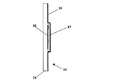
図2は、本発明の実施形態に従う素子15の断面図である。素子15は、第1電極16と、圧電層17と、第2電極18と、絶縁層24とを具えている。この実施形態において、絶縁層24は、電極16、18及び圧電層17の構造支持体及び基板として作用する。第1電極16、圧電層17及び第2電極18は圧力波トランスデューサを形成している。第2電極18は又、コンデンサのプレートを形成している。圧電層とは、機械的ひずみにより電気を生成する一方、逆に、印加された電界の効果により膨張或いは収縮する層のことである。絶縁層24は電気的絶縁体である。絶縁層24は、セラミック、例えばアルミナタイルとすることができる。第1電極16は15μm厚で、表面積は10mm×10mmであり、この表面積が圧力波トランスデューサの全体寸法を規定しているが、これは大きい方の第2電極18の寸法を制限するものではない。第2電極18も又15μm厚であるが、表面積は35mm×35mmである。図面は実物大ではなく、単に説明に役立つものとして意図されているということに留意されたい。第1電極16と第2電極18とは実質的に平行であり、50μm厚の圧電層17を共に挟んでいる。
Next, embodiments of the present invention will be described with reference to the accompanying drawings.
FIG. 2 is a cross-sectional view of
第1電極16、圧電層17及び第2電極18は全て、周知の方法、例えば、ペーストをスクリーン印刷してから該ペーストを焼成して厚膜層を形成することによって、基板24に沈着させる。第1電極16は、金ペースト(イングランド、リーディング所在エレクトロサイエンスラボラトリーズ製ESL8836金ペースト)として沈着させ、それから焼成して強固な厚膜を形成する。そして圧電層17は、0−3複合体、ジルコン酸チタン酸鉛厚膜ペースト(PZT型5A/ガラスペースト、サウサンプトン大学作成、イングランド、サウサンプトン所在モーガンエレクトロセラミックによって提供された原材料、PZT材料の分類「5A」に属する)として第1電極16の上に沈着させ(又、図示した例では、該電極16を超えて延びている)、それから焼成する。「0−3」という用語は、該複合体の構成結合材料が互いに直交するx、y及びz軸に沿って接続されていないが、構成圧電材料がこれらの互いに直交する軸の全てに沿って活性であるという事実を言っている。第2電極18は、金ペースト(ESL8836金ペースト)として沈着させ、それから焼成し、これによって、第1電極16と、絶縁層24と、第2電極18との間で圧電層17を挟む厚膜を形成する。厚膜が利用されてきたのは、それらがコンパクトで、強固で、比較的安価であると共に、1つの装置に圧力波トランスデューサとコンデンサとを組み合わせたものを作製するのに十分万能であるからである。厚膜は、水のような高温流体を含む環境での使用に特に適している。
The
図3は、本発明の第1実施形態に従う装置の断面図を示す。この場合において、前記素子15は厚膜形状でアルミナタイル24に沈着しており、該アルミナタイルは鋼製支持体21に実装されて前記素子に十分な剛性及び支持を付与している。前記装置は、図2に示す如き素子を2つ、第1素子15と第2素子19とを具えている。第2素子19は第1素子15と実質的に同一であり、第1電極16aと、圧電層17aと、第2電極18aとを具えている。この実施形態における第1素子15と同様、第2素子は、鋼製支持体21aに実装されたアルミナタイル24aに厚膜形状で沈着させている。
FIG. 3 shows a cross-sectional view of the device according to the first embodiment of the present invention. In this case, the
実装された両素子は互いに対向して配置され、第1素子15の第2電極18が第2素子19の第2電極18aに対向している。両素子は互いに20mm離間されている。第1素子15の第2電極18は第2素子19の第2電極18aに接続され、これによってコンデンサを形成している。
Both mounted elements are arranged to face each other, and the
前記両素子は、保護層、通常は素子の外表面に沈着させたエポキシ層(図示省略)に被覆されていてもよい。これにより、装置が物理的に厳しい動作環境で用いられる場合に幾らか保護され、保護層が装置の性能に悪影響を及ぼさないように好都合に薄い層を利用することができる。保護層は、ブラッシング又はスクレイピング等どのような好都合な手段によって沈着させてもよい。このような層を例えば0.1mm厚のエポキシ層とすることもできる。 Both elements may be covered with a protective layer, usually an epoxy layer (not shown) deposited on the outer surface of the element. This provides some protection when the device is used in physically demanding operating environments, and a thin layer can be advantageously used so that the protective layer does not adversely affect the performance of the device. The protective layer may be deposited by any convenient means such as brushing or scraping. Such a layer may be an epoxy layer having a thickness of 0.1 mm, for example.
前記装置は、圧力波又は静電容量測定を用いて関心領域を特徴付けるために用いることができる。このような領域が装置の2つの素子の中間にくるように該装置を配置することによって特徴付けが達成される。 The device can be used to characterize a region of interest using pressure waves or capacitance measurements. Characterization is achieved by positioning the device so that such a region is midway between the two elements of the device.
このような関心領域は、流体、又は複数の流体及び/又は固体微粒子を含む不均一混合物であってもよい。このような関心領域の特徴付けは、2つの相補的測定、即ち、該領域を通過する超音波の伝達及び該領域の静電容量の測定を用いることによって達成される。関心領域を通過する超音波の速度を測定することによって、構成材料の割合を抽出することができる。静電容量測定は、関心領域の誘電率における特性を特定するために使用される。誘電率の変化によって生じる静電容量全体の変化は、不均一混合物における相間の界面に対応するものである。 Such a region of interest may be a fluid or a heterogeneous mixture comprising a plurality of fluids and / or solid particulates. Such characterization of the region of interest is accomplished by using two complementary measurements: transmission of ultrasound through the region and measurement of the capacitance of the region. By measuring the speed of the ultrasonic wave passing through the region of interest, the proportion of the constituent material can be extracted. Capacitance measurements are used to identify characteristics in the dielectric constant of the region of interest. The change in overall capacitance caused by the change in dielectric constant corresponds to the interface between the phases in the heterogeneous mixture.
各素子は2つの電気接続部(図示省略)を有し、1つは第1電極16、16aに、1つは第2電極18、18aに接続されている。該電気接続部は更に、電気信号処理及び電気信号生成手段に接続されている。電気信号処理手段は、電極での信号を検出して素子間の静電容量を決定するため、及び/又は素子に起こる圧力波を検出するために利用される。電気信号生成手段は、素子15、19の1つの素子の両電極16、16a、18、18aに電気接続部を通して適切な電気信号を供給して圧力波を生成するために利用される。第1素子15を圧力波のアクチュエータとして用いると、第1及び第2電極16、18により圧電層17に亘って変動する電界が印加される。該電界は、圧力波を生成するように圧電層17を膨張及び収縮させるのに十分な周波数のものである。好ましくは、該周波数は超音波周波数(即ち20,000Hzを超える周波数)であり、これによって事実上超音波である圧力波を生成する。従って、第2素子19はセンサとして動作する。第2素子19の第2電極18aに作用する圧力波がこれを運動させる。このような運動により第2素子19の圧電層17aが膨張及び収縮し、これによって電気エネルギーを生成する。このように、第1及び第2電極18a、16a間に変動する電界が形成され、圧力波の検出が可能になる。発生した電気エネルギーを測定することによって、検出された圧力波を特徴付けることができる。
Each element has two electrical connections (not shown), one connected to the
静電容量測定は、第1素子15の第2電極18と第2素子19の第2電極18aとを電気的に接続することによって形成されたようなコンデンサを用いて行なうことができる。このような静電容量測定は順番に、或いは圧力波測定と平行して行なうことができる。
The capacitance measurement can be performed using a capacitor formed by electrically connecting the
前記装置は単に例として説明したものであり、特許請求の範囲によって得られる保護を超えないであろう様々な変形を前記装置に行なってもよいということが当業者には自明であろう。 It will be apparent to those skilled in the art that the apparatus has been described by way of example only and that various modifications may be made to the apparatus that would not exceed the protection afforded by the claims.
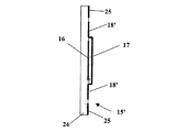
例えば、感知部品を電気的損傷から保護するために図2に示した素子15を変形することができるということが理解されるであろう。図5a及び図5bはそれぞれ、本発明の他の実施形態に従う素子15’の断面図及び平面図である。該素子15’は、図2を参照して説明したものと同様のものである。同一の参照符号を用いて同様の特徴を示している。しかしながら、この実施形態において、第2電極18’は表面積において図2のそれより小さい。又、第2電極18’の周囲に、しかしそれと接触しないで、ガードリング25が配置されている。該ガードリング25は、金ペースト等の厚膜導電体として沈着させる。使用時、ガードリング25はどのような容量ピックアップでも消散させ、これによって、それが包囲している電極が望ましくない電荷を蓄積することから保護している。
For example, it will be appreciated that the
ここまで、図2の素子15を参照して前記装置を説明したが、図5a及び5bを参照して説明した素子15’をこのような装置に実施することもできるということは容易に理解されるであろう。
Up to now, the device has been described with reference to
更に、前記装置は様々な寸法のものであってもよいということが理解されるであろう。例えば、それぞれの層の表面積は上述のものと異なっていてもよい。2つの素子の移動は、一方の素子の、他方によって生成された超音波を検出する能力によって制限されるのみである。該移動は、素子の構成層の寸法、そして又、特徴付けされるべき関心領域(例えば流体)の特性の機能である。 It will further be appreciated that the device may be of various dimensions. For example, the surface area of each layer may be different from that described above. The movement of the two elements is only limited by the ability of one element to detect the ultrasound generated by the other. The movement is a function of the dimensions of the component layers of the device and also the properties of the region of interest (eg fluid) to be characterized.
又、前記装置を構成する素子の圧電層として、0−3複合体同様、例えば、1−3複合体又は3−3複合体等の他の圧電材料を使用してもよいということが理解されるであろう。更に、圧電層は必ずしも厚膜性質のものでなくても、焼結セラミック又はポリマー圧電体等の他の材料から作製してもよいということが理解されるであろう。同じ機能性を有する装置を薄膜から作製してもよい。化学蒸着又はスパッタリング技術によって薄膜を沈着させてもよい。加えて、プラチナ又は銀等、金以外の金属から電極を作製してもよい。 Further, it is understood that other piezoelectric materials such as a 1-3 composite or a 3-3 composite may be used as the piezoelectric layer of the elements constituting the device, like the 0-3 composite. It will be. Furthermore, it will be appreciated that the piezoelectric layer is not necessarily of thick film nature and may be made from other materials such as sintered ceramics or polymeric piezoelectrics. Devices with the same functionality may be made from thin films. Thin films may be deposited by chemical vapor deposition or sputtering techniques. In addition, the electrodes may be made from a metal other than gold, such as platinum or silver.
更に、上述の例における絶縁層24は、2つの金属層、即ち第1及び第2電極間の電気的接続を防止するように配備されているということが理解されるであろう。他の構成において、別個の絶縁層は不要であるということが理解されるであろう。例えば、圧電層は、実質的に第2電極の下を延びてそれを第1電極から絶縁していてもよい。
Furthermore, it will be appreciated that the insulating
本発明の更なる実施形態を図4に示す。ここで、図3に示す如き複数の装置が長手方向に配置されている。これらの装置は、隣り合う装置の鋼製支持体21、21a が互いに平行で一線に沿うように配置されている。この実施形態において、鋼製支持体21、21aは連続した支持体を形成している。この実施形態において、前記連続した支持体はチューブとして整形されており、該チューブの表面内の隙間は、各装置を形成している両素子間にチューブの外側から物質を流すことができるようになっている。 A further embodiment of the present invention is shown in FIG. Here, a plurality of devices as shown in FIG. 3 are arranged in the longitudinal direction. These apparatuses are arranged so that the steel supports 21 and 21a of the adjacent apparatuses are parallel to each other and along a line. In this embodiment, the steel supports 21, 21a form a continuous support. In this embodiment, the continuous support is shaped as a tube, and the gap in the surface of the tube allows the material to flow from the outside of the tube between the elements forming each device. It has become.
図示の如く、これらの装置を形成している複数対の素子は装置の長手軸23に沿って離間しており、一対内の各素子は前記軸の両側に配備されている。
As shown, the pairs of elements forming these devices are spaced along the
使用時、複数の関心領域を同時に特徴付けることができる。従って、前記複数の装置を図1のオイルセパレータ船舶に設置し、複数の関心領域を特徴付け、更に、相間の不明瞭な界面を特徴付け、決定するために用いることができる。 In use, multiple regions of interest can be characterized simultaneously. Accordingly, the plurality of devices can be installed in the oil separator vessel of FIG. 1 and used to characterize and determine areas of interest and to characterize and determine indistinct interfaces between phases.
装置自体の、上述の材料及び寸法の変更同様、上に例示したもの以外の方法で前記複数の装置を配置してもよいということが当業者には理解されるであろう。前記複数の装置は、例えばアレイ又はマトリクス状の構造を形成することもできる。このような構造は多くの形をとることができる。 Those skilled in the art will appreciate that the devices may be arranged in ways other than those illustrated above, as well as the material and dimensional changes described above for the devices themselves. The plurality of devices may form an array or matrix structure, for example. Such a structure can take many forms.
例えば、複数の装置を線状に或いは長手方向に配置して、簡易な1次元の装置のアレイを形成してもよい。複数の1次元のアレイを前記線上配置の方向に直交する方向に配置して、装置の2次元アレイを形成してもよい。前記線状及び2次元の繰り返しの両方に直交する方向に前記2次元アレイを繰り返して、3次元アレイを形成してもよい。 For example, a plurality of devices may be arranged linearly or in the longitudinal direction to form a simple one-dimensional device array. A plurality of one-dimensional arrays may be arranged in a direction orthogonal to the linear arrangement direction to form a two-dimensional array of devices. The two-dimensional array may be repeated in a direction orthogonal to both the linear and two-dimensional repetitions to form a three-dimensional array.
Claims (18)
前記素子はそれぞれ、
第1電極と、
第2電極と、
第1電極と第2電極との間に介在してこれらに接続された圧電層
とを具えている感知装置において、
各素子の第1電極、第2電極及び圧電層は圧力波トランスデューサを形成し、
第1及び第2素子は、第1素子の第2電極が第2素子の第2電極と対向するように配置され、両第2電極がコンデンサのプレートを形成するように前記両素子を互いに離間させる感知装置。 Comprising a first element and a second element;
Each of the elements is
A first electrode;
A second electrode;
In a sensing device comprising a piezoelectric layer interposed between and connected to a first electrode and a second electrode,
The first electrode, the second electrode and the piezoelectric layer of each element form a pressure wave transducer,
The first and second elements are arranged such that the second electrode of the first element faces the second electrode of the second element, and the two elements are separated from each other so that both second electrodes form a capacitor plate. Sensing device.
第1素子の第1及び第2電極を経て、前記第1装置の圧電層を横切り、該圧電層を膨張或いは収縮させ、これによって圧力波を生成するように第1電界を印加することと、
第2素子の圧電層の膨張又は収縮及び結果として第2素子の第1及び第2電極に発生する第2電界を介して前記圧力波を検出することと、
第1素子の第2電極及び第2素子の第2電極を介して、両第2電極間の前記領域の静電容量を測定すること
とを含む感知方法。 Operating a sensing device according to any one of the preceding claims, wherein both devices of the device are arranged on both sides of a region of interest.
Applying a first electric field through the first and second electrodes of the first element across the piezoelectric layer of the first device and expanding or contracting the piezoelectric layer, thereby generating a pressure wave;
Detecting the pressure wave via expansion or contraction of the piezoelectric layer of the second element and, as a result, a second electric field generated in the first and second electrodes of the second element;
Measuring the capacitance of the region between the second electrodes via the second electrode of the first element and the second electrode of the second element.
第2電極と、
第1電極と第2電極との間に介在してこれらに接続された圧電層
とを具えた感知素子において、
前記素子の第1電極、第2電極及び圧電層は圧力波トランスデューサを形成し、第2電極はコンデンサのプレートを形成する感知素子。 A first electrode;
A second electrode;
In a sensing element comprising a piezoelectric layer interposed between and connected to a first electrode and a second electrode,
The first electrode, the second electrode and the piezoelectric layer of the element form a pressure wave transducer, and the second electrode forms a capacitor plate.
圧電層を沈着させることと、
第3層を沈着させ、これによって第2電極を形成して、第1及び第3層が圧電層を挟むようにすること
とを含む、素子の製造の方法。 Depositing a first layer, thereby forming a first electrode;
Depositing a piezoelectric layer;
Depositing a third layer, thereby forming a second electrode such that the first and third layers sandwich the piezoelectric layer.
Applications Claiming Priority (2)
| Application Number | Priority Date | Filing Date | Title |
|---|---|---|---|
| GBGB0320168.8A GB0320168D0 (en) | 2003-08-28 | 2003-08-28 | A sensing device |
| PCT/GB2004/003805 WO2005022106A1 (en) | 2003-08-28 | 2004-08-27 | Pressure wave piezoelectric sensor |
Publications (1)
| Publication Number | Publication Date |
|---|---|
| JP2007504440A true JP2007504440A (en) | 2007-03-01 |
Family
ID=28686492
Family Applications (1)
| Application Number | Title | Priority Date | Filing Date |
|---|---|---|---|
| JP2006524429A Pending JP2007504440A (en) | 2003-08-28 | 2004-08-27 | Pressure wave piezoelectric sensor |
Country Status (9)
| Country | Link |
|---|---|
| US (1) | US7499377B2 (en) |
| EP (1) | EP1660854B1 (en) |
| JP (1) | JP2007504440A (en) |
| AT (1) | ATE456789T1 (en) |
| CA (1) | CA2537223A1 (en) |
| DE (1) | DE602004025358D1 (en) |
| GB (1) | GB0320168D0 (en) |
| NO (1) | NO20061409L (en) |
| WO (1) | WO2005022106A1 (en) |
Families Citing this family (6)
| Publication number | Priority date | Publication date | Assignee | Title |
|---|---|---|---|---|
| GB0320168D0 (en) * | 2003-08-28 | 2003-10-01 | Univ Manchester | A sensing device |
| US20120250679A1 (en) * | 2011-03-29 | 2012-10-04 | Amazon Technologies, Inc. | Network Transpose Box and Switch Operation Based on Backplane Ethernet |
| US9996199B2 (en) * | 2012-07-10 | 2018-06-12 | Electronics And Telecommunications Research Institute | Film haptic system having multiple operation points |
| US8939906B2 (en) * | 2013-03-18 | 2015-01-27 | National Chiao Tung University | Wireless intraocular pressure monitoring device, and detecting module thereof |
| FR3012255B1 (en) * | 2013-10-17 | 2017-03-10 | Commissariat Energie Atomique | PROCESS FOR FORMING WRINKLES BY FUSIONING A FOUNDATION ON WHICH RESTORATES A CONSTRAINED LAYER |
| GB202005065D0 (en) * | 2020-04-06 | 2020-05-20 | Atout Process Ltd | Electrical capacitance tomography apparatus, systems and methods |
Citations (7)
| Publication number | Priority date | Publication date | Assignee | Title |
|---|---|---|---|---|
| US2963641A (en) * | 1958-08-01 | 1960-12-06 | Shell Oil Co | Exploration of earth formations associated with petroleum deposits |
| GB1354865A (en) * | 1971-07-08 | 1974-06-05 | Inst Francais Du Petrole | Pressure wave piezoelectric sensor |
| US3832762A (en) * | 1972-05-22 | 1974-09-03 | Texas Instruments Inc | Method of producing a matched parameter acceleration cancelling hydrophone |
| US4011748A (en) * | 1975-09-18 | 1977-03-15 | The Board Of Trustees Of Leland Stanford Junior University | Method and apparatus for acoustic and optical scanning of an object |
| US4398539A (en) * | 1980-06-30 | 1983-08-16 | Second Foundation | Extended focus transducer system |
| JPH0523694B2 (en) * | 1987-10-27 | 1993-04-05 | Nippon Kokan Kk | |
| JP2002209292A (en) * | 2001-01-11 | 2002-07-26 | Matsushita Electric Ind Co Ltd | Ultrasonic probe |
Family Cites Families (8)
| Publication number | Priority date | Publication date | Assignee | Title |
|---|---|---|---|---|
| US2963642A (en) * | 1958-08-01 | 1960-12-06 | Shell Oil Co | Method and apparatus for determining directional dielectric anisotropy in solids |
| FR2634088B1 (en) * | 1988-07-11 | 1991-05-31 | Inst Francais Du Petrole | PIEZOELECTRIC SENSOR COMPRISING AT LEAST ONE PAIR OF FLEXIBLE SENSITIVE ELEMENTS OF LONG LENGTH |
| US4954811A (en) * | 1988-11-29 | 1990-09-04 | Pennwalt Corporation | Penetration sensor |
| US5251627A (en) * | 1991-06-27 | 1993-10-12 | Morris Donald E | Non-invasive measurement of eyeball pressure using vibration |
| US5329496A (en) * | 1992-10-16 | 1994-07-12 | Duke University | Two-dimensional array ultrasonic transducers |
| ATE263388T1 (en) | 1997-08-02 | 2004-04-15 | Univ Manchester | FLOW CONTROL SYSTEM |
| JP2002538431A (en) * | 1999-02-25 | 2002-11-12 | メタセンサーズ インコーポレイテッド | Real-time fluid analysis device and method |
| GB0320168D0 (en) * | 2003-08-28 | 2003-10-01 | Univ Manchester | A sensing device |
-
2003
- 2003-08-28 GB GBGB0320168.8A patent/GB0320168D0/en not_active Ceased
-
2004
- 2004-08-27 DE DE602004025358T patent/DE602004025358D1/en active Active
- 2004-08-27 JP JP2006524429A patent/JP2007504440A/en active Pending
- 2004-08-27 CA CA002537223A patent/CA2537223A1/en not_active Abandoned
- 2004-08-27 WO PCT/GB2004/003805 patent/WO2005022106A1/en active Application Filing
- 2004-08-27 AT AT04768352T patent/ATE456789T1/en not_active IP Right Cessation
- 2004-08-27 US US10/569,899 patent/US7499377B2/en not_active Expired - Fee Related
- 2004-08-27 EP EP04768352A patent/EP1660854B1/en not_active Not-in-force
-
2006
- 2006-03-28 NO NO20061409A patent/NO20061409L/en not_active Application Discontinuation
Patent Citations (7)
| Publication number | Priority date | Publication date | Assignee | Title |
|---|---|---|---|---|
| US2963641A (en) * | 1958-08-01 | 1960-12-06 | Shell Oil Co | Exploration of earth formations associated with petroleum deposits |
| GB1354865A (en) * | 1971-07-08 | 1974-06-05 | Inst Francais Du Petrole | Pressure wave piezoelectric sensor |
| US3832762A (en) * | 1972-05-22 | 1974-09-03 | Texas Instruments Inc | Method of producing a matched parameter acceleration cancelling hydrophone |
| US4011748A (en) * | 1975-09-18 | 1977-03-15 | The Board Of Trustees Of Leland Stanford Junior University | Method and apparatus for acoustic and optical scanning of an object |
| US4398539A (en) * | 1980-06-30 | 1983-08-16 | Second Foundation | Extended focus transducer system |
| JPH0523694B2 (en) * | 1987-10-27 | 1993-04-05 | Nippon Kokan Kk | |
| JP2002209292A (en) * | 2001-01-11 | 2002-07-26 | Matsushita Electric Ind Co Ltd | Ultrasonic probe |
Also Published As
| Publication number | Publication date |
|---|---|
| EP1660854A1 (en) | 2006-05-31 |
| WO2005022106A1 (en) | 2005-03-10 |
| US20070007861A1 (en) | 2007-01-11 |
| ATE456789T1 (en) | 2010-02-15 |
| GB0320168D0 (en) | 2003-10-01 |
| DE602004025358D1 (en) | 2010-03-18 |
| NO20061409L (en) | 2006-03-28 |
| EP1660854B1 (en) | 2010-01-27 |
| US7499377B2 (en) | 2009-03-03 |
| CA2537223A1 (en) | 2005-03-10 |
Similar Documents
| Publication | Publication Date | Title |
|---|---|---|
| US9898640B2 (en) | Capacitive fingerprint sensing device and method for capturing a fingerprint using the sensing device | |
| US7791248B2 (en) | Piezoelectric composite based on flexoelectric charge separation | |
| Muralt et al. | Piezoelectric micromachined ultrasonic transducers based on PZT thin films | |
| EP3079837B1 (en) | Monolithically integrated three electrode cmut device | |
| US7759839B2 (en) | Acoustic decoupling in cMUTs | |
| US9821340B2 (en) | High displacement ultrasonic transducer | |
| EP0174897B1 (en) | Underwater piezoelectric arrangement | |
| CN105310715B (en) | Piezoelectric device, ultrasonic device, imaging apparatus, probe, and electronic apparatus | |
| US7581295B2 (en) | Piezoelectric element and method of manufacturing the same | |
| JP6953513B2 (en) | Micro pressure sensor | |
| WO2016115363A1 (en) | Piezoelectric transducers and methods of making and using the same | |
| WO2014134723A1 (en) | Capacitive micromachined ultrasonic transducer with multiple deflectable membranes | |
| EP2939281A1 (en) | Piezoelectric devices | |
| JP2007504440A (en) | Pressure wave piezoelectric sensor | |
| Pang et al. | A transparent capacitive micromachined ultrasonic transducer (CMUT) array for finger hover-sensing dial pads | |
| Cai et al. | A transfer matrix approach for acoustic analysis of a multilayered active acoustic coating | |
| Jung et al. | A top-crossover-to-bottom addressed segmented annular array using piezoelectric micromachined ultrasonic transducers | |
| Thränhardt et al. | A resonant CMUT sensor for fluid applications | |
| Decharat et al. | High frequency copolymer ultrasonic transducer array of size-effective elements | |
| JP2017005661A (en) | Ultrasonic vibrator and ultrasonic diagnostic apparatus | |
| CN107421655A (en) | A kind of even order Lamb wave generating means and system for detecting temperature | |
| Mo et al. | The effect of electrode pattern on the behavior of piezoelectric actuators in a circular diaphragm structure | |
| Ravi et al. | Modeling and Simulation of Dual Application Capacitive MEMS Sensor | |
| You et al. | Direction of arrival estimation using asymmetric mode components of CMUTs | |
| CN107275473B (en) | Transducer having at least one electrode of a first type, an electrode of a second type and at least one ferroelectret |
Legal Events
| Date | Code | Title | Description |
|---|---|---|---|
| A621 | Written request for application examination |
Free format text: JAPANESE INTERMEDIATE CODE: A621 Effective date: 20070807 |
|
| A131 | Notification of reasons for refusal |
Free format text: JAPANESE INTERMEDIATE CODE: A131 Effective date: 20100903 |
|
| A02 | Decision of refusal |
Free format text: JAPANESE INTERMEDIATE CODE: A02 Effective date: 20110301 Free format text: JAPANESE INTERMEDIATE CODE: A02 Effective date: 20110301 |