JP2007273631A - Method of detecting end position of probe and storage medium recorded therewith, and probe device - Google Patents
Method of detecting end position of probe and storage medium recorded therewith, and probe device Download PDFInfo
- Publication number
- JP2007273631A JP2007273631A JP2006095822A JP2006095822A JP2007273631A JP 2007273631 A JP2007273631 A JP 2007273631A JP 2006095822 A JP2006095822 A JP 2006095822A JP 2006095822 A JP2006095822 A JP 2006095822A JP 2007273631 A JP2007273631 A JP 2007273631A
- Authority
- JP
- Japan
- Prior art keywords
- transparent film
- probe
- height
- substrate
- probes
- Prior art date
- Legal status (The legal status is an assumption and is not a legal conclusion. Google has not performed a legal analysis and makes no representation as to the accuracy of the status listed.)
- Granted
Links
Images


Classifications
-
- H—ELECTRICITY
- H01—ELECTRIC ELEMENTS
- H01L—SEMICONDUCTOR DEVICES NOT COVERED BY CLASS H10
- H01L22/00—Testing or measuring during manufacture or treatment; Reliability measurements, i.e. testing of parts without further processing to modify the parts as such; Structural arrangements therefor
-
- G—PHYSICS
- G01—MEASURING; TESTING
- G01R—MEASURING ELECTRIC VARIABLES; MEASURING MAGNETIC VARIABLES
- G01R31/00—Arrangements for testing electric properties; Arrangements for locating electric faults; Arrangements for electrical testing characterised by what is being tested not provided for elsewhere
- G01R31/28—Testing of electronic circuits, e.g. by signal tracer
- G01R31/2851—Testing of integrated circuits [IC]
- G01R31/2886—Features relating to contacting the IC under test, e.g. probe heads; chucks
- G01R31/2891—Features relating to contacting the IC under test, e.g. probe heads; chucks related to sensing or controlling of force, position, temperature
Abstract
Description
本発明は、半導体ウエハ等の被検査体の電気的特性検査を行う際に使用するプローブの先端位置の検出方法、この方法を記録した記憶媒体、及びプローブ装置に関し、更に詳しくは、プローブカードの複数のプローブそれぞれの先端位置を高精度に検出することができ、延いては検査の信頼性を高めることができるプローブの先端位置の検出方法、この方法を記録した記憶媒体、及びプローブ装置に関するものである。 The present invention relates to a method for detecting the tip position of a probe used when inspecting an electrical property of an object to be inspected such as a semiconductor wafer, a storage medium recording the method, and a probe device. BACKGROUND OF THE INVENTION 1. Field of the Invention The present invention relates to a probe tip position detection method capable of detecting the tip positions of each of a plurality of probes with high accuracy, and thus improving the reliability of inspection, a storage medium recording this method, and a probe apparatus. It is.
プローブカードを用いて半導体ウエハ等の被検査体の電気的特性検査を行う場合には、例えばカメラを介してプローブカードに設けられた複数のプローブの先端を撮像し、プローブの先端位置を検出し、被検査体の電極とプローブとを接触させて検査を行う。カメラを用いたプローブの先端位置の検出には、プローブの先端にカメラの焦点を合わせるのに時間が掛かり、この結果被検査体とプローブカードのアライメントに多くに時間を割かざるを得ないため、通常、全てのプローブについて行わず、例えば代表的な数本のプローブを選択して行われている。しかし、電極が微細化した場合、全プローブがそれぞれの電極にうまく当たらない可能性が出てくるため、可能な限り全プローブの先端の位置を検出できる方が、プローブとウエハとのアライメントを行う場合に好ましい。 When using a probe card to inspect the electrical characteristics of an object to be inspected, such as a semiconductor wafer, for example, the tip of a plurality of probes provided on the probe card is imaged via a camera to detect the tip position of the probe. The inspection is performed by bringing the electrode of the object to be inspected into contact with the probe. Detection of the tip position of the probe using a camera takes time to focus the camera on the tip of the probe, and as a result, it takes much time to align the object to be inspected and the probe card. Usually, it does not carry out about all the probes, for example, it carries out by selecting several typical probes. However, when the electrodes are miniaturized, there is a possibility that all the probes do not hit each electrode well. Therefore, it is possible to detect the position of the tip of all the probes as much as possible to align the probe and the wafer. Preferred in some cases.
また、複数のプローブカードメーカーから様々な種類のプローブカードが開発されるため、その都度、複数のプローブを三次元で画像認識する専用のアルゴリズムを開発する必要がある。これに対応するには莫大な費用がかかるため、二次元のフィルム上に複数のプローブを転写することができれば、アルゴリズムの開発を容易に行うことができる。 In addition, since various types of probe cards are developed by a plurality of probe card manufacturers, it is necessary to develop a dedicated algorithm for recognizing a plurality of probes in three dimensions each time. Since it takes enormous costs to cope with this, if a plurality of probes can be transferred onto a two-dimensional film, an algorithm can be easily developed.
そこで、特許文献1にはプローブの検出時間を短縮したプローブ検査方法及びプローブ検査装置について記載されている。この技術では、検査前にプローブカードの複数のプローブの先端跡を変形体に転写し、この針跡開口の大きさに基づいてプローブの電極への押し込み深さを算出し、更にプローブの位置合わせを短縮している。また、プローブの先端跡及びプローブの押し込み深さを測定する手段として静電容量を利用した位置センサが記載されている。また、この文献1にはマトリックス状に配列された電極を有する位置センサを用いて複数のプローブのX、Y座標位置を検出することについて記載されている。 Therefore, Patent Document 1 describes a probe inspection method and a probe inspection apparatus that shorten the probe detection time. In this technology, the tip traces of multiple probes on the probe card are transferred to a deformed body before inspection, and the depth of probe probe push-in is calculated based on the size of the needle trace opening. Is shortened. Further, a position sensor using capacitance is described as means for measuring the probe tip trace and the probe push-in depth. Further, this document 1 describes that X, Y coordinate positions of a plurality of probes are detected using a position sensor having electrodes arranged in a matrix.
また、特許文献2にはエラストマー組成物からなるプローブ位置調整用フィルムについて記載されている。このプローブ位置調整用フィルムにプローブを接触させて傷跡を付け、この傷跡と集積回路の電極部との位置関係を確認し、必要に応じて傷跡と電極部との関係からプローブの位置を調整する。 Patent Document 2 describes a probe position adjusting film made of an elastomer composition. A probe is brought into contact with the probe position adjusting film to make a scar, the positional relationship between the scar and the electrode part of the integrated circuit is confirmed, and the position of the probe is adjusted from the relation between the scar and the electrode part as necessary. .
また、特許文献3には位置合わせ方法について記載されている。この方法では、探針の針跡をダミーウエハ上に付けてカメラで検出することにより探針の方向と設定位置を認識する。
特許文献4には検査方法について記載されている。この方法では、載置台横の支持台に配された転写シートに熱膨張したプローブを圧接して転写シートに針跡を付け、転写シートの針跡を検出した後、熱膨張後のプローブとウエハとを位置合わせするようにしている。 Patent Document 4 describes an inspection method. In this method, a thermally expanded probe is pressed against a transfer sheet placed on a support table next to the mounting table to create a needle mark on the transfer sheet, and after detecting the needle mark on the transfer sheet, the probe and wafer after thermal expansion are detected. Are aligned with each other.
また、特許文献5には半導体検査方法について記載されている。この方法では、載置台上に透明樹脂部材からなるプレートを供給し、プレートに針跡を付け、この針跡の画像情報に基づいて駆動部が駆動して載置台上の半導体素子と検査針との位置合わせを行う。 Patent Document 5 describes a semiconductor inspection method. In this method, a plate made of a transparent resin member is supplied onto the mounting table, a needle mark is provided on the plate, and a drive unit is driven based on image information of the needle mark, so that a semiconductor element and an inspection needle on the mounting table are provided. Perform position alignment.
また、特許文献6にはプローブ検査方法について記載されている。この方法では、載置台の横に配置された小片の中央に形成されたX、Y方向の基準点となる十字マークをターゲットとして載置台のX、Y、θ方向の位置を認識する。更に、Z方向の位置についてはターゲットの周辺に形成された導電性薄膜と静電容量センサとで認識する。そして、検査を行う時には、最初のチップの電極パッドに生じた針跡をCCDカメラで検出し、この針跡に基づいてその後の検査を実行するか否かを判断している。
しかしながら、特許文献1の技術の場合には、変形体に形成されたプローブ痕によりプローブの針先位置やプローブの押し込み深さを知ることができるが、変形体ではプローブと被検査体との位置関係を知ることができない。また、特許文献2の技術の場合には、プローブによってプローブ位置調整用フィルムに傷跡を付けることで、傷跡と集積回路の電極部の位置関係を確認できると記載されているが、傷跡と電極部の位置関係を確認する手法について具体的には一切言及されていない。 However, in the case of the technique of Patent Literature 1, the probe tip formed on the deformable body and the probe tip position and the probe push-in depth can be known. I can't know the relationship. In the case of the technique of Patent Document 2, it is described that the positional relationship between the scar and the electrode portion of the integrated circuit can be confirmed by making a scar on the probe position adjusting film with a probe. No specific mention is made of a method for confirming the positional relationship between the two.
また、特許文献3、4の技術では、いずれもダミーウエハや転写シートに複数のプローブの針跡を付け、ウエハの載置台を移動させて、これらの針跡を一つずつ撮像手段で検出するため、載置台の移動回数が多くなるほど移動量の誤差が累積されて、後の針跡ほど検出精度が悪くなる。
Further, in the techniques of
また、特許文献5の技術もプレートに載置台上の一部にプレートを供給し、このプレートに複数の検査針の針跡を付けてプローブの位置を検出する点では特許文献3、4の技術と共通している。また、特許文献6に技術は検査時に最初のチップの電極パッドに直接針跡を付けて、その後の検査を実行する2回目以降の検査を実行するか判断するため、事前に複数のプローブとウエハ全面の電極パッドとの位置関係を確認することはできない。
In the technique of Patent Document 5, the technique is disclosed in
本発明は、上記課題を解決するためになされたもので、高温時であっても複数のプローブと被検査体の検査用電極との位置関係を高速且つ高精度に検出することができ、もって電気的特性検査の信頼性を高めることができるプローブの先端位置の検出方法、この方法を記録した記憶媒体、及びプローブ装置を提供することを目的としている。 The present invention has been made to solve the above-described problems, and can detect the positional relationship between a plurality of probes and inspection electrodes of an object to be inspected at high speed and with high accuracy even at high temperatures. It is an object of the present invention to provide a probe tip position detection method capable of improving the reliability of electrical characteristic inspection, a storage medium recording this method, and a probe device.
本発明の請求項1に記載のプローブの先端位置の検出方法は、被検査体に複数のプローブを電気的に接触させて上記被検査体の電気的特性検査を行うに当たり、上記複数のプローブの先端の位置を検出する方法であって、上記被検査体と同一配列の電極を複数有する基板に透明フィルムを貼り付ける第1の工程と、第1の工程で得られた上記基板の複数の電極を、撮像手段を用いて上記透明フィルム越しに検出する第2の工程と、上記透明フィルムの表面高さを付与する第3の工程と、第2の工程で検出された上記基板の電極と上記複数のプローブとの位置合わせを行う第4の工程と、上記表面高さに基づいて上記複数のプローブと上記透明フィルムとを接触させて上記透明フィルムに針跡を付ける第5の工程と、上記複数の電極と上記透明フィルムの針跡に基づいて上記複数のプローブの先端の位置を検出する第6の工程と、を備えたことを特徴とするものである。 According to a first aspect of the present invention, there is provided a method for detecting a tip position of a probe, wherein when a plurality of probes are brought into electrical contact with an object to be inspected and an electrical characteristic inspection of the object to be inspected is performed, A method for detecting a position of a tip, a first step of attaching a transparent film to a substrate having a plurality of electrodes of the same arrangement as the object to be inspected, and a plurality of electrodes of the substrate obtained in the first step Is detected through the transparent film using an imaging means, a third step of imparting a surface height of the transparent film, the electrode of the substrate detected in the second step, and the above A fourth step of performing alignment with a plurality of probes, a fifth step of bringing the plurality of probes and the transparent film into contact with each other based on the surface height, and applying a needle mark to the transparent film; Multiple electrodes and transparent Based on the needle marks of Irumu it is characterized in that and a sixth step of detecting the position of the tip of the probes.
また、本発明の請求項2に記載のプローブの先端位置の検出方法は、請求項1に記載の発明において、上記第3の工程では、接触センサを上記透明フィルムの表面に接触させて、上記透明フィルムの表面高さを求めることを特徴とするものである。 The probe tip position detection method according to claim 2 of the present invention is the method according to claim 1, wherein in the third step, the contact sensor is brought into contact with the surface of the transparent film, The surface height of the transparent film is obtained.
また、本発明の請求項3に記載のプローブの先端位置の検出方法は、請求項1に記載の発明において、上記第3の工程では、上記撮像手段を用いて上記基板の見掛け上の高さと実際の高さとを測定し、この高低差と上記透明フィルムの屈折率とに基づいて上記透明フィルムの表面高さを求めることを特徴とするものである。 According to a third aspect of the present invention, there is provided a method for detecting a tip position of a probe according to the first aspect of the present invention, wherein, in the third step, the apparent height of the substrate is determined using the imaging means. The actual height is measured, and the surface height of the transparent film is obtained based on the height difference and the refractive index of the transparent film.
また、本発明の請求項4に記載のプローブの先端位置の検出方法は、請求項1〜請求項3のいずれか1項に記載の発明において、上記第4の工程に先立って、上記透明フィルムの表面高さに基づいて上記基板のオーバードライブ量を設定することを特徴とするものである。 Moreover, the detection method of the front-end | tip position of the probe of Claim 4 of this invention is the invention of any one of Claims 1-3. WHEREIN: Prior to the said 4th process, the said transparent film The overdrive amount of the substrate is set based on the surface height of the substrate.
また、本発明の請求項5に記載のプローブの先端位置の検出方法は、請求項3または請求項4に記載の発明において、上記第3の工程に先立って、上記接触センサを用いて上記基板の透明フィルムの厚さを測定し、また、上記撮像手段を用いて測定される上記基板の見掛け上の高さと実際の高さとの差を上記基板の高さの補正値として求め、上記透明フィルムの厚さと上記補正値に基づいて上記透明フィルムの屈折率を求め、上記屈折率に基づいて上記透明フィルムの表面高さを付与することを特徴とすることを特徴とするものである。 According to a fifth aspect of the present invention, there is provided a method for detecting the tip position of a probe according to the third or fourth aspect, wherein the substrate is used by using the contact sensor prior to the third step. The thickness of the transparent film is measured, and the difference between the apparent height of the substrate measured using the imaging means and the actual height is obtained as a correction value for the height of the substrate, and the transparent film The refractive index of the transparent film is obtained based on the thickness of the film and the correction value, and the surface height of the transparent film is imparted based on the refractive index.
また、本発明の請求項6に記載のプローブの先端位置の検出方法は、請求項1に記載の発明において、予め、上記接触センサを用いて厚さの異なる上記透明フィルムの厚さを測定し、また、上記撮像手段を用いて上記各透明フィルムについて測定される上記基板の見掛け上の高さと実際の高さとの差を補正値として求め、上記各透明フィルムの厚さと上記各透明フィルムの補正値との相関関係に基づいて測定される上記基板の見掛け上の高さと実際の高さとの差から上記透明フィルムの表面高さを付与することを特徴とするものである。 The probe tip position detection method according to claim 6 of the present invention is the method according to claim 1, wherein the thicknesses of the transparent films having different thicknesses are measured in advance using the contact sensor. Further, the difference between the apparent height of the substrate and the actual height measured for each transparent film using the imaging means is obtained as a correction value, and the thickness of each transparent film and the correction for each transparent film are obtained. The surface height of the transparent film is given from the difference between the apparent height of the substrate measured based on the correlation with the value and the actual height.
また、本発明の請求項7に記載のプローブの先端位置の検出方法は、請求項1〜請求項6のいずれか1項に記載の発明において、上記基板から上記透明フィルムを剥離する第6の工程を備えたことを特徴とするものである。 A probe tip position detection method according to a seventh aspect of the present invention is the sixth aspect of the invention according to any one of the first to sixth aspects, wherein the transparent film is peeled from the substrate. It is characterized by comprising a process.
また、本発明の請求項8に記載のプローブの先端位置の検出方法は、請求項7に記載の発明において、上記第6の工程に先立って、上記透明フィルムに紫外線を照射することを特徴とするものである。 The probe tip position detecting method according to claim 8 of the present invention is characterized in that, in the invention according to claim 7, the transparent film is irradiated with ultraviolet rays prior to the sixth step. To do.
また、本発明の請求項9に記載の記憶媒体は、コンピュータを駆動させて、請求項1〜請求項8のいずれか1項に記載のプローブの先端位置の検出方法を実行させることを特徴とするものである。 According to a ninth aspect of the present invention, there is provided a storage medium that drives a computer to execute the probe tip position detection method according to any one of the first to eighth aspects. To do.
また、本発明の請求項10に記載のプローブ装置は、制御装置の制御下で、被検査体に複数のプローブを接触させて上記被検査体の電気的特性検査を行うに当たり、上記被検査体と同一配列の電極を複数有する基板に貼り付けられた透明フィルムに上記複数のプローブの針跡を付けてこれらの針跡に基づいて上記複数のプローブの先端を検出するプローブ装置であって、上記基板を撮像する撮像手段と、上記透明フィルムの表面高さを付与する手段と、上記撮像手段を用いて上記透明フィルム越しに上記基板を撮像して上記複数の電極と上記複数のプローブとの位置合わせを行う手段と、上記表面高さに基づいて上記複数のプローブと上記透明フィルムとを接触させて上記透明フィルムに針跡を付ける手段と、上記複数の電極と上記透明フィルムの針跡に基づいて上記複数のプローブの先端の位置を検出する手段と、を備えたことを特徴とするものである。 According to a tenth aspect of the present invention, there is provided a probe device comprising: a plurality of probes that are in contact with an object to be inspected to perform an electrical characteristic inspection on the object to be inspected; A probe device that attaches needle traces of the plurality of probes to a transparent film affixed to a substrate having a plurality of electrodes of the same arrangement and detects the tips of the plurality of probes based on the needle traces, Image pickup means for picking up an image of the substrate, means for giving the surface height of the transparent film, and positions of the plurality of electrodes and the plurality of probes by picking up the image of the substrate through the transparent film using the image pickup means Means for aligning, means for bringing the plurality of probes and the transparent film into contact with each other on the basis of the surface height, and making needle marks on the transparent film; the plurality of electrodes; and the transparent film. Based on the arm of the needle marks it is characterized in further comprising a means for detecting the position of the tip of the probes.
また、本発明の請求項11に記載のプローブ装置は、請求項10に記載の発明において、上記透明フィルムの表面に接触し、上記透明フィルムの表面高さを検出する接触センサを備えたことを特徴とするものである。
The probe device according to
また、本発明の請求項12に記載のプローブ装置は、請求項10に記載の発明において、上記制御装置は、上記撮像手段を用いて測定された上記基板の見掛け上の高さと実際の高さとの高低差と上記透明フィルムの屈折率とに基づいて上記透明フィルムの表面高さを算出する手段を有することを特徴とするものである。 According to a twelfth aspect of the present invention, in the probe device according to the tenth aspect of the present invention, the control device includes an apparent height and an actual height of the substrate measured using the imaging unit. And a means for calculating the surface height of the transparent film based on the difference in height and the refractive index of the transparent film.
また、本発明の請求項13に記載のプローブ装置は、請求項10〜請求項12のいずれか1項に記載の発明において、上記制御装置は、上記透明フィルムの表面高さに基づいて上記基板のオーバードライブ量を設定指令する手段を有することを特徴とするものである。 The probe device according to a thirteenth aspect of the present invention is the probe device according to any one of the tenth to twelfth aspects, wherein the control device is configured such that the substrate is based on a surface height of the transparent film. And a means for commanding the setting of the overdrive amount.
また、本発明の請求項14に記載のプローブ装置は、請求項12または請求項13に記載の発明において、上記制御装置は、上記接触センサの検出値に基づいて上記基板の透明フィルムの厚さを算出する手段と、上記撮像手段を用いて測定された上記基板の見掛け上の高さと実際の高さとの差を上記基板の高さの補正値として求める手段と、上記透明フィルムの厚さと上記補正値に基づいて上記透明フィルムの屈折率を求める手段と、を有することを特徴とするものである。 According to a fourteenth aspect of the present invention, in the probe device according to the twelfth or thirteenth aspect of the invention, the control device is configured such that the thickness of the transparent film on the substrate is determined based on a detection value of the contact sensor. Means for calculating the difference between the apparent height of the substrate measured using the imaging means and the actual height as a correction value for the height of the substrate, the thickness of the transparent film, and the above Means for obtaining the refractive index of the transparent film based on a correction value.
また、本発明の請求項15に記載のプローブ装置は、請求項10〜請求項14のいずれか1項に記載の発明において、上記制御装置は、上記接触センサを用いて測定された複数の上記透明フィルムの厚さをそれぞれ記憶する手段と、上記撮像手段を用いて上記各透明フィルムについて測定された上記基板の見掛け上の高さと実際の高さとの差を補正値として記憶する手段と、上記各透明フィルムの厚さと上記各透明フィルムの補正値との相関関係に基づいて測定される上記基板の見掛け上の高さと実際の高さとの差から上記透明フィルムの表面高さを付与する手段と、を有することを特徴とするものである。 According to a fifteenth aspect of the present invention, in the probe device according to any one of the tenth to fourteenth aspects, the control device includes a plurality of the measurement devices measured using the contact sensor. Means for storing the thickness of each transparent film; means for storing a difference between the apparent height of the substrate measured for each transparent film using the imaging means and the actual height as a correction value; and Means for giving the surface height of the transparent film from the difference between the actual height and the apparent height of the substrate measured based on the correlation between the thickness of each transparent film and the correction value of each transparent film; , Characterized by having.
また、本発明の請求項16に記載のプローブ装置は、請求項10〜請求項15のいずれか1項に記載の発明において、上記透明フィルムに紫外線を照射する手段を備えたことを特徴とするものである。 Moreover, the probe apparatus according to claim 16 of the present invention is characterized in that in the invention according to any one of claims 10 to 15, the transparent film is provided with means for irradiating ultraviolet rays. Is.
本発明の請求項1〜請求項16に記載の発明によれば、高温時であっても複数のプローブと被検査体の検査用電極との位置関係を高速且つ高精度に検出することができ、もって電気的特性検査の信頼性を高めることができるプローブの先端位置の検出方法、この方法を記録した記憶媒体、及びプローブ装置を提供することができる。 According to the first to sixteenth aspects of the present invention, the positional relationship between the plurality of probes and the inspection electrodes of the object to be inspected can be detected at high speed and with high accuracy even at high temperatures. Therefore, it is possible to provide a probe tip position detection method, a storage medium recording the method, and a probe apparatus that can improve the reliability of the electrical characteristic inspection.
以下、図1〜図8に示す実施形態に基づいて本発明を説明する。 Hereinafter, the present invention will be described based on the embodiment shown in FIGS.
第1の実施形態
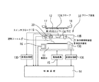
まず、本発明のプローブ装置について説明する。本実施形態のプローブ装置10は、例えば図1に示すように、被検査体であるウエハ(図示せず)を載置する移動可能な載置台11と、この載置台11の上方に配置されたプローブカード12と、このプローブカード12の複数のプローブ12Aと載置台11上のウエハとのアライメントを行うアライメント機構13と、載置台11及びアライメント機構13等を制御する制御装置14と、を備え、制御装置14の制御下でアライメント機構13が駆動して、載置台11上のウエハとプローブカード12の複数のプローブ12Aとのアライメントを行った後、複数のプローブ12Aとウエハとを電気的に接触させてウエハの電気的特性検査を行うように構成されている。本実施形態において、プローブ12Aの針跡を検出する場合には、同図に示すようにウエハに代えて透明フィルムFが貼り付けられた基板(検出用基板)Wを載置台11に載置する。
First Embodiment First, a probe apparatus of the present invention will be described. For example, as shown in FIG. 1, the probe apparatus 10 according to the present embodiment is arranged on a movable mounting table 11 on which a wafer (not shown) as an object to be inspected is mounted, and above the mounting table 11. A
載置台11は、制御装置14の制御下で駆動する駆動機構15を介してX、Y、Z及びθ方向に移動するように構成されている。載置台11の側方には荷重センサ(ロードセル)16が配置され、例えばプローブ12Aとの接触により、プローブ12A先端の高さを検出するようにしてある。プローブカード12は、カードホルダ17を介してプローバ室のヘッドプレート18に取り付けられ、オートレベリング機構(図示せず)を介して水平度を出すようにしてある。
The mounting table 11 is configured to move in the X, Y, Z, and θ directions via a
また、アライメント機構13は、載置台11にロードセル16から周方向へ偏倚させて配置された第1の撮像手段(CCDカメラ)13Aと、アライメントブリッジ13Bに固定された第2の撮像手段(CCDカメラ)13Cと、を備えて構成されている。第1のCCDカメラ13Aは、アライメントブリッジ13Bを介してプローバ室の最奥部からプローブセンタまで進出してプローブカード12と載置台11との間に位置し、ここで載置台11がX、Y方向へ移動する間に、ウエハの検査用電極を上方から検出して撮像し、その画像処理部13Dで画像処理して制御装置14へ画像信号を送信する。第2のCCDカメラ13Cは、プローブカードの下方で載置台11がX、Y方向へ移動する間に、プローブカード12の下方から複数のプローブ12Aを順次検出して撮像し、その画像処理部13Eで画像処理して制御装置14へ画像信号を送信する。
The alignment mechanism 13 includes a first imaging unit (CCD camera) 13A disposed on the mounting table 11 while being deviated from the
また、アライメントブリッジ13Bには接触センサ(スイッチプローブ)19が取り付けられ、スイッチプローブ19によって載置台11上の検出用基板W等の表面高さを検出するようにしてある。また、アライメントブリッジ13Bにはレーザー測長器20及び紫外線照射装置21が取り付けられている。レーザー測長器19は、例えばロードセル16の表面高さを測定し、紫外線照射装置21は本発明のプローブの先端位置の検出方法で使用される透明フィルムの粘着剤を劣化させて透明フィルムを検出用基板Wから剥れ易くする。
A contact sensor (switch probe) 19 is attached to the
また、制御装置14は、中央演算処理装置及び記憶装置を備え、本発明のプローブの先端位置の検出方法を実行する際に、中央演算処理装置においてプローブ装置10の各構成機器との間で種々の情報信号を送受信し、種々の演算処理を行い、その演算処理結果等の各種の情報を記憶装置において記憶する。記憶装置は主記憶装置及び補助記憶装置からなる。補助記憶装置には本発明のプローブの先端位置の検出方法を実行するための記憶媒体が格納されている。
The
次に、本発明のプローブの先端位置の検出方法の実施形態について図2〜図8を参照しながら説明する。 Next, an embodiment of the probe tip position detection method of the present invention will be described with reference to FIGS.
本実施形態のプローブの先端位置の検出方法は、ウエハの電気的特性検査に先立って実施される。この検出方法では、実際の検査対象となるウエハと同一に配列された電極を有する基板をプローブの針先位置の検出用基板として用いる。そこで、以下では検査用基板にも符号Wを附して説明する。 The method for detecting the tip position of the probe of this embodiment is performed prior to the inspection of the electrical characteristics of the wafer. In this detection method, a substrate having electrodes arranged in the same manner as the wafer to be actually inspected is used as a substrate for detecting the probe tip position. Therefore, in the following description, the inspection substrate is also denoted by the reference symbol W.
本実施形態の方法では、例えば図2に示すように検出用基板Wの電極側の面に透明フィルムを貼り付け、この検出用基板Wの複数の電極Pとこれらに対応するプローブ12Aとのアライメントを行った後、複数のプローブ12Aで透明フィルムFにプローブ12Aの針跡Mを付ける。そして、第1のCCDカメラ13A(図1参照)を用いて、検出用基板Wをインデックス送りしながら透明フィルムF越しに検出用基板Wの電極P及び針跡Mを同時に検出する。このように実際のウエハと同一配列の電極Pを有する検出用基板Wを用いて電極Pと針跡Mを同時に観察するため、針跡Mと検出用基板Wの電極Pと関連付けながら高精度且つ同時に検出することができる。従って、ように、転写シート等に付けられた複数の針跡に合わせて載置台を移動させて一つずつ針跡を検出する従来の方法と比較すれば、載置台の送りによる累積誤差がない。
In the method of the present embodiment, for example, as shown in FIG. 2, a transparent film is attached to the electrode-side surface of the detection substrate W, and alignment between the plurality of electrodes P of the detection substrate W and the
そこで、本実施形態のプローブの先端位置の検出方法を図3〜図8をも参照しながら更に詳細に説明する。 Therefore, the method for detecting the tip position of the probe according to this embodiment will be described in more detail with reference to FIGS.
まず、図2に示すように検出用基板Wの表面に透明フィルムFを貼り付ける。透明フィルムFは、塑性変形し、その形態を維持できる素材によって形成されている。このような素材として、例えばエチレンビニルアセテート(EVA)やポリエチレンテレフタレート(PET)等の合成樹脂が好ましく用いられる。EVAは例えば−40〜+70℃前後で使用され、PETは例えば70℃以上で使用される。 First, as shown in FIG. 2, a transparent film F is attached to the surface of the detection substrate W. The transparent film F is formed of a material that can be plastically deformed and maintain its form. As such a material, for example, a synthetic resin such as ethylene vinyl acetate (EVA) or polyethylene terephthalate (PET) is preferably used. EVA is used at, for example, around −40 to + 70 ° C., and PET is used at, for example, 70 ° C. or higher.
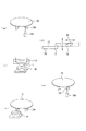
そして、検出用基板Wをプローブ装置10の載置台11へ載置する。そして、検出用基板Wとプローブカード12の複数のプローブ12Aとのアライメントを行う前に、図3の(a)〜(e)に示すようにプローブカード12の水平度をチェックする。
Then, the detection substrate W is mounted on the mounting table 11 of the probe apparatus 10. Before the alignment between the detection substrate W and the plurality of
それにはまず、図3の(a)に示すように、プローブカード12の下方で載置台11を移動させ、載置台11に固定された第2のCCDカメラ13Cによってプローブカード12の複数のプローブ12AのX、Y位置を検出する。その後、同図の(b)に示すように、アライメントブリッジ13Bがプローブセンタまで進出した後、載置台11のロードセル16がアライメントブリッジ13Bのレーザー測長器19の真下になるように載置台11が移動し、レーザー測長器19からレーザー光Lをロードセル16に向けて照射し、基準位置にあるロードセル16の表面高さを測長した後、アライメントブリッジ13Bがプローブセンタから退避する。これらの測定結果を制御装置14の補助記憶装置へ記憶する。
First, as shown in FIG. 3A, the mounting table 11 is moved below the
その後、図3の(c)に示すように、制御装置14の制御下でロードセル16が四隅のプローブ12Aに一本ずつ接触するように載置台11が順次移動し、これらのプローブ12Aをロードセル16で順次検出する。制御装置14では中央演算処理装置においてロードセル16がその基準位置との関係からプローブ12Aの先端位置を求める。四隅のプローブ12Aの先端位置の間に高低差があると、制御装置14の制御下でこれらの高低差に基づいて同図の(d)に示すようにオートレベリング機構22が駆動し、プローブカード12が水平になるように調整する。引き続き、同図の(e)に示すように第2のCCDカメラ13Cで四隅のプローブ12Aの先端位置を検出し、これらのプローブ12Aが同一高さになったことを確認する。そして、この高さを制御装置14の補助記憶装置へ記憶する。これら一連の動作でプローブカード12の水平を出した後、図4の(a)〜(d)に示すように検出用基板Wの電極Pとプローブカード12の複数のプローブ12Aとのアライメントを行う。
Thereafter, as shown in FIG. 3C, the mounting table 11 sequentially moves so that the
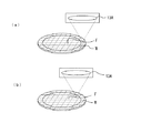
それにはまず、図4の(a)に示すように、アライメントブリッジ13Bがプローブセンタへ進出した後、検出用基板Wが第1のCCDカメラ13Aの真下になるように載置台11が移動する。そして、制御装置14の制御下で載置台11が検出用基板Wのインデックス送りを行って、第1のCCDカメラ13Aで検出用基板Wの複数の電極を透明フィルムF越しにそれぞれ検出する。これにより、検出用基板Wと複数のプローブ12Aとのアライメントを終了する。その後、制御装置14の制御下で載置台11が上昇し、透明フィルムFと複数のプローブ12Aとが接触し、透明フィルムFの表面に針跡Mを付ける。透明フィルムFに針跡Mを付けるためには、載置台11上における透明フィルムFの表面高さを求めて、制御装置14に与えなくてはならない。
For this purpose, first, as shown in FIG. 4A, after the
そこで、本実施形態では、図4の(b)に示すようにアライメントブリッジ13Bに取り付けられたスイッチプローブ19を使用して透明フィルムFの表面高さを検出する。それには載置台11に固定された第2のCCDカメラ13Cを用いてスイッチプローブ19の先端高さを検出する。次いで、載置台11がスイッチプローブ19の真下まで移動した後、載置台11が上昇して透明フィルムFとスイッチプローブ19とが接触する。制御装置14では、中央演算処理装置において第2のCCDカメラ13Cでスイッチプローブ19を検出した時の載置台11の高さと、透明フィルムFの表面を検出した時の載置台11の高さに基づいて透明フィルムFの表面高さを算出し、その表面高さを補助記憶装置に記憶する。
Therefore, in the present embodiment, the surface height of the transparent film F is detected using the
そして、制御装置14の中央演算処理装置においてプローブ12Aの高さと透明フィルムFの表面高さとの差を求め、この差分だけ制御装置14を介して載置台11を上昇させることにより、同図の(c)に示すように検出用基板Wとプローブ12Aとが接触し、更に制御装置14の制御下で予め設定されたオーバードライブ量だけ載置台11が上昇すると、図2に示すように透明フィルムFの表面に針跡Mを付けることができる。
Then, the central processing unit of the
引き続き、同図の(d)に示すように制御装置14の制御下で、アライメントブリッジ13Bがプローブセンタへ進出し、第1のCCDカメラ13Aの下方で載置台11が高速度でインデックス送りされると、制御装置14では第1のCCDカメラ13Aを介して検出用基板Wの電極Pと透明フィルムFの針跡Mを同時に高速に認識することができる。この結果に基づいて、検出用基板Wの電極Pと針跡Mとの位置ズレ等の位置関係を正確に知ることができる。そして、透明フィルムFから検出されたプローブ12の先端位置の位置データを制御装置14の補助記憶装置に記録しておくことにより、ウエハの電極パッドとプローブ12Aとを正確にアライメントすることができ、検査の信頼性を高めることができる。
Subsequently, as shown in FIG. 6D, under the control of the
上述のようにして透明フィルムFを使用してプローブ12Aの針跡Mと検出用基板Wの電極Pとの関係からプローブ12Aの先端位置を検出した後、アライメントブリッジ13Bがプローブセンタへ進出する。そして、載置台11が移動してアライメントブリッジ13Bの紫外線照射装置21の真下に検出用基板Wの中心部を配置する。そして、図5の(a)に矢印で示すように紫外線照射装置21から透明フィルムFに紫外線を照射して透明フィルムFの粘着剤を劣化させる。これにより同図の(b)に示すように透明フィルムFが検出用基板Wから簡単に剥がせる状態になる。その後、載置台11から検出用基板Wを取り出し、検査用基板Wを損傷することなく検査用基板Wから透明フィルムFを簡単に剥離することができ、検出用基板Wを繰り返し使用することができる。
After detecting the tip position of the
以上説明したように本実施形態によれば、ウエハの検査を行う前に行うプローブの先端位置を検出する方法として、ウエハと同一配列の電極Pを複数有する検出用基板Wに透明フィルムFを貼り付ける第1の工程と、この検出用基板Wの複数の電極Pを、第1のCCDカメラ13Aを用いて透明フィルムF越しに検出する第2の工程と、スイッチプローブ16を用いて透明フィルムFの表面高さを検出する第3の工程と、検出用基板Wの複数の電極Pと複数のプローブ12Aとの位置合わせを行う第4の工程と、透明フィルムFの表面高さに基づいて載置台11を上昇させて複数のプローブ12Aと透明フィルムFとを接触させて透明フィルムFに針跡Mを付ける第5の工程と、検出用基板Wの複数の電極Pと透明フィルムFの針跡Mに基づいて複数のプローブ12Aの先端の位置を検出する第6の工程と、を備えているため、高温時であっても、検出用基板Wに高精度に形成された電極Pを利用して、載置台11を高速でインデックス送りすることで、第1のCCDカメラ13Aによって全てのプローブ12Aの先端位置を高速且つ高精度に検出することができ、その後のウエハの検査工程ではウエハの複数の電極パッドと、これらの電極パッドに対応する複数のプローブ12Aと位置ズレなく正確に電気的に接触させることができ、延いては信頼性の高い検査を行うことができる。また、紫外線照射装置10によって透明フィルムF越しに検査用基板Wに紫外線を照射することにより、透明フィルムFを検出用基板Wから簡単に剥離することができ、検出用基板Wを繰り返し使用することができる。
As described above, according to the present embodiment, as a method for detecting the tip position of the probe performed before the wafer inspection, the transparent film F is pasted on the detection substrate W having a plurality of electrodes P in the same array as the wafer. A first step of attaching, a second step of detecting the plurality of electrodes P of the detection substrate W through the transparent film F using the
第2の実施形態
上記実施形態では第3の工程でスイッチプローブ16を使用して透明フィルムFの表面高さを直接測定する場合について説明したが、本実施形態では第3の工程では透明フィルムFの屈折率を利用して透明フィルムFの表面高さを求めた後プローブの位置を検出する点に特徴がある。透明フィルムFの屈折率を利用して透明フィルムFの表面高さを求めること以外は第1の実施形態と同一であるため、本実施形態の特徴について説明する。
Second Embodiment In the above embodiment, a case has been described in which the surface height of the transparent film F is directly measured using the
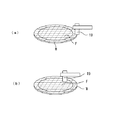
第1のCCDカメラ13Aで透明フィルムF越しに検出用基板Wの電極Pを検出すると、図2、図6の(a)に示すように透明フィルムFにおいて光が屈折し、実際の検出用基板Wの表面高さを検出することができず、制御装置14では図6の(b)に示すように検出用基板Wの見掛け上の表面高さを検出する。しかも、第1のCCDカメラ13Aは透明フィルムFの表面を検出することができないため、実際の透明フィルムFの表面高さが判らない。そこで、透明フィルムFの屈折率を利用することで、検出用基板Wの見掛け上の表面高さに補正を加えて実際の表面高さを求めることができる。尚、図6の(a)、(b)では針跡及び電極は省略されている。
When the
即ち、第1のCCDカメラ13Aの開口数N.A.(=sinθ)は既知であるため、この開口数と透明フィルムFの屈折率nによって透明フィルムFの厚さL1を制御装置14の中央演算処理装置において求めることができる。透明フィルムFの屈折率をnとすると、図5の(b)に示す関係から、下記の式1が成立する。
L1*tanφ=(L1+L2)*tanθ・・・式1
式1において、tanφ、tanθは既知であり、L2は第1のCCDカメラ13Aによって測定することができる。即ち、図7の(a)に示すように第1のカメラ13Aによって透明フィルムFの外側で検出用基板Wを検出すると、図6の(b)の一点鎖線の位置にある検査用基板Wの表面高さを実際に検出する。この時の載置台11の位置を補助記憶装置に記憶する。次いで、載置台11を移動させて第1のCCDカメラ13Aによって透明フィルムF越し検出用基板Wを検出すると、図6の(a)にある検出用基板Wを検出することができる。この時の載置台11の位置を補助記憶装置に記憶する。中央演算処理装置において図6の(a)に示す検出位置から同図の(b)に示す検出位置を差し引くと、L2を求めることができる。ここで、tanφ、tanθ及びL2が既知であるから、これらの値を式1に代入することによってL1、即ち透明フィルムFの厚さを求めることができる。
That is, the numerical aperture N.I. A. Since (= sin θ) is known, the central processing unit of the
L1 * tanφ = (L1 + L2) * tanθ Equation 1
In Equation 1, tan φ and tan θ are known, and L2 can be measured by the
従って、透明フィルムF越しに検出用基板Wを検出した時の図6の(b)に示す検出用基板Wの見掛け上の表面高さに補正値L2で表面高さを補正することによって透明フィルムF越しの検出用基板Wの実際の高さを求めることができる。更に、式1によって求めた透明フィルムFの厚さL1を加算することによって透明フィルムFの表面高さを計算によって求めることができる。このように検出用基板Wの表面高さと透明フィルムFの表面高さから、検査用基板Wのオーバードライブ量を正確に設定することができる。後は、第1の実施形態と同一の手順に従って透明フィルムFの表面にプローブ12Aの針跡Mを付けることができる。即ち、透明フィルムFの屈折率nが既知であれば、第1のCCDカメラ13Aを使用すれば透明フィルムFの表面高さを計算によって求めることができ、検出用基板Wのオーバードライブ量をも正確に設定することができる。その他、第1の実施形態と同様の作用効果を期することができる。
Therefore, the transparent film is corrected by correcting the surface height with the correction value L2 to the apparent surface height of the detection substrate W shown in FIG. 6B when the detection substrate W is detected through the transparent film F. The actual height of the detection substrate W over F can be obtained. Furthermore, the surface height of the transparent film F can be obtained by calculation by adding the thickness L1 of the transparent film F obtained by Equation 1. Thus, the amount of overdrive of the inspection substrate W can be accurately set from the surface height of the detection substrate W and the surface height of the transparent film F. Thereafter, the needle trace M of the
また、透明フィルムFの厚さL1は、図8の(a)、(b)に示すようにスイッチプローブ19を使用することによって求めることができる。即ち、同図の(a)に示すようにスイッチプローブ19を透明フィルムFの外側で検出用基板Wに接触させて、検出用基板Wの表面高さを検出する。次いで、載置台11を移動させて透明フィルムFの上方にスイッチプローブ19を配置し、載置台11を上昇させて透明フィルムFとスイッチプローブ19とを接触させて、透明フィルムFの表面高さを検出する。透明フィルムFの表面高さから検出用基板Wの表面高さを差し引くことで透明フィルムFの厚さL1を求めることができる。
Further, the thickness L1 of the transparent film F can be obtained by using the
従って、第1のCCDカメラ13Aとスイッチプローブ19を使用することによって透明フィルムFの表面高さを簡単に求めることができる。
Therefore, the surface height of the transparent film F can be easily obtained by using the
第3の実施形態
本実施形態は透明フィルムFの屈折率nが未知の場合に、透明フィルムFの屈折率nを求める点に特徴がある。この場合には透明フィルムFの屈折率nが未知であるため、式1から明らかなように透明フィルムFの厚さL1及び検査用基板Wの高さの補正値L2を測定により求めなくてはならない。
Third Embodiment The present embodiment is characterized in that the refractive index n of the transparent film F is obtained when the refractive index n of the transparent film F is unknown. In this case, since the refractive index n of the transparent film F is unknown, the thickness L1 of the transparent film F and the correction value L2 of the height of the inspection substrate W must be obtained by measurement as is apparent from Equation 1. Don't be.
それには、第1のCCDカメラ13Aを使用して図7の(a)、(b)に示す方法で検査用基板Wの高さの補正値L2を求めると共に、スイッチプローブ19を使用して図8の(a)、(b)に示す方法で透明フィルムFの厚さL1を求める。第1のCCDカメラ13Aの開口数は既知であるから、これらの値を式1に代入することによりtanφを求めることができる。ここで透明フィルムFの屈折率はn=sinθ/sinφで表され、この式とtanφから屈折率nを求めることができる。
For this purpose, the
透明フィルムFの厚さL1及び屈折率nは、温度によって変化するため、上記の各方法によって、ある厚さの透明フィルムFの厚さと温度のとの相関関係及び屈折率nと温度との相関関係を求めておき、補助記憶装置に記憶させておくことができる。そうすると、任意の検査温度における、ある厚さの透明フィルムFの厚さL1及び屈折率nはそれぞれの相関関係から簡単に求めることができ、延いては透明フィルムFの表面高さが簡単に求めることができる。 Since the thickness L1 and the refractive index n of the transparent film F change depending on the temperature, the correlation between the thickness and the temperature of the transparent film F having a certain thickness and the correlation between the refractive index n and the temperature are obtained by the above methods. The relationship can be obtained and stored in the auxiliary storage device. Then, the thickness L1 and the refractive index n of the transparent film F having a certain thickness at an arbitrary inspection temperature can be easily obtained from the respective correlations, and thus the surface height of the transparent film F is easily obtained. be able to.
また、厚さの異なる複数の透明フィルムFを用意し、それぞれの透明フィルムFについてスイッチプローブ19を用いてそれぞれの透明フィルムFの厚さを測定し、また、第1のCCDカメラ13Aを用いて透明フィルムFの補正値L2を測定する。そして、これらの値から式1に基づいて透明フィルタFの屈折率nを算出する。そして、横軸に透明フィルムFの厚さL1を取り、縦軸に補正値L2を取って、これらの両者の相関関係を求めておく。これにより、各透明フィルムの厚さL1と上記各透明フィルムの補正L2との相関関係に基づいて測定される検出用基板Wの見掛け上の高さと実際の高さとの差から透明フィルムの表面高さを付与することができる。
In addition, a plurality of transparent films F having different thicknesses are prepared, the thickness of each transparent film F is measured using the
更に、式1を用いて透明フィルムFの厚さL1と検出用基板Wの補正値L2との相関関係を求めることができる。この相関関係により、任意の厚さに対する補正値L2を簡単に求めることができ、延いては透明フィルムFの実際の表面高さを簡単に求めることができる。 Furthermore, the correlation between the thickness L1 of the transparent film F and the correction value L2 of the detection substrate W can be obtained using Equation 1. By this correlation, the correction value L2 for an arbitrary thickness can be easily obtained, and the actual surface height of the transparent film F can be easily obtained.
尚、本発明は上記各実施形態に何等制限されるものではなく、必要に応じて各構成要素を適宜変更することができる。 In addition, this invention is not restrict | limited at all to said each embodiment, Each component can be changed suitably as needed.
本発明は、半導体ウエハ等の被検査体の電気的特性検査を行うプローブ装置に好適に利用することができる。 INDUSTRIAL APPLICABILITY The present invention can be suitably used for a probe apparatus that performs an electrical property inspection of an object to be inspected such as a semiconductor wafer.
10 プローブ装置
11 載置台
12 プローブカード
12A プローブ
13A 第1のCCDカメラ(撮像手段)
14 制御装置
19 スイッチプローブ(接触センサ)
21 紫外線照射装置
DESCRIPTION OF SYMBOLS 10
14
21 UV irradiation equipment
Claims (16)
上記被検査体と同一配列の電極を複数有する基板に透明フィルムを貼り付ける第1の工程と、
第1の工程で得られた上記基板の複数の電極を、撮像手段を用いて上記透明フィルム越しに検出する第2の工程と、
上記透明フィルムの表面高さを付与する第3の工程と、
第2の工程で検出された上記基板の電極と上記複数のプローブとの位置合わせを行う第4の工程と、
上記表面高さに基づいて上記複数のプローブと上記透明フィルムとを接触させて上記透明フィルムに針跡を付ける第5の工程と、
上記複数の電極と上記透明フィルムの針跡に基づいて上記複数のプローブの先端の位置を検出する第6の工程と、を備えた
ことを特徴とするプローブの先端位置の検出方法。 A method of detecting the positions of the tips of the plurality of probes when performing electrical property inspection of the inspection object by electrically contacting a plurality of probes with the inspection object,
A first step of attaching a transparent film to a substrate having a plurality of electrodes of the same arrangement as the test object;
A second step of detecting the plurality of electrodes of the substrate obtained in the first step through the transparent film using an imaging means;
A third step of imparting a surface height of the transparent film;
A fourth step of aligning the electrodes of the substrate detected in the second step with the plurality of probes;
A fifth step of bringing the plurality of probes and the transparent film into contact with each other based on the height of the surface to make a needle mark on the transparent film;
And a sixth step of detecting the positions of the tips of the plurality of probes based on the plurality of electrodes and the needle marks of the transparent film.
上記基板を撮像する撮像手段と、
上記透明フィルムの表面高さを付与する手段と、
上記撮像手段を用いて上記透明フィルム越しに上記基板を撮像して上記複数の電極と上記複数のプローブとの位置合わせを行う手段と、
上記表面高さに基づいて上記複数のプローブと上記透明フィルムとを接触させて上記透明フィルムに針跡を付ける手段と、
上記複数の電極と上記透明フィルムの針跡に基づいて上記複数のプローブの先端の位置を検出する手段と、を備えた
ことを特徴とするプローブ装置。 Under the control of the control device, a plurality of probes are brought into contact with the object to be inspected to conduct an electrical property inspection of the object to be inspected. A probe device that attaches needle traces of the plurality of probes to a film and detects the tips of the plurality of probes based on these needle traces,
Imaging means for imaging the substrate;
Means for imparting a surface height of the transparent film;
Means for imaging the substrate through the transparent film using the imaging means and aligning the plurality of electrodes and the plurality of probes;
Means for contacting the plurality of probes with the transparent film based on the surface height to make a needle mark on the transparent film;
A probe device comprising: a plurality of electrodes; and means for detecting positions of tips of the plurality of probes based on needle traces of the transparent film.
Priority Applications (4)
| Application Number | Priority Date | Filing Date | Title |
|---|---|---|---|
| JP2006095822A JP4996119B2 (en) | 2006-03-30 | 2006-03-30 | Probe tip position detection method, storage medium recording this method, and probe apparatus |
| TW096111079A TWI431703B (en) | 2006-03-30 | 2007-03-29 | A method of detecting the leading position of the probe, and a recording medium and a probe device for recording the method |
| KR1020070030961A KR100881237B1 (en) | 2006-03-30 | 2007-03-29 | Detection method of probe's tip location, storage medium storing the method, and probe device |
| US11/694,100 US7397257B2 (en) | 2006-03-30 | 2007-03-30 | Detection method/device of probe's tip location using a transparent film attached to a substate having plurality of electrodes, and a storage medium for implementing the method |
Applications Claiming Priority (1)
| Application Number | Priority Date | Filing Date | Title |
|---|---|---|---|
| JP2006095822A JP4996119B2 (en) | 2006-03-30 | 2006-03-30 | Probe tip position detection method, storage medium recording this method, and probe apparatus |
Publications (3)
| Publication Number | Publication Date |
|---|---|
| JP2007273631A true JP2007273631A (en) | 2007-10-18 |
| JP2007273631A5 JP2007273631A5 (en) | 2009-05-21 |
| JP4996119B2 JP4996119B2 (en) | 2012-08-08 |
Family
ID=38557909
Family Applications (1)
| Application Number | Title | Priority Date | Filing Date |
|---|---|---|---|
| JP2006095822A Active JP4996119B2 (en) | 2006-03-30 | 2006-03-30 | Probe tip position detection method, storage medium recording this method, and probe apparatus |
Country Status (4)
| Country | Link |
|---|---|
| US (1) | US7397257B2 (en) |
| JP (1) | JP4996119B2 (en) |
| KR (1) | KR100881237B1 (en) |
| TW (1) | TWI431703B (en) |
Cited By (4)
| Publication number | Priority date | Publication date | Assignee | Title |
|---|---|---|---|---|
| WO2010029637A1 (en) * | 2008-09-12 | 2010-03-18 | 株式会社島津製作所 | Probe pin contact checking apparatus and liquid crystal substrate inspection apparatus |
| KR20150131495A (en) * | 2014-05-15 | 2015-11-25 | 삼성전자주식회사 | Probing apparatus and operating method thereof |
| CN105513990A (en) * | 2015-12-07 | 2016-04-20 | 杭州长川科技股份有限公司 | Probe station image positioning device and vision alignment method |
| US9995786B2 (en) | 2015-11-17 | 2018-06-12 | Mitsubishi Electric Corporation | Apparatus and method for evaluating semiconductor device |
Families Citing this family (16)
| Publication number | Priority date | Publication date | Assignee | Title |
|---|---|---|---|---|
| KR20110027641A (en) * | 2008-02-26 | 2011-03-16 | 덴끼 가가꾸 고교 가부시키가이샤 | Probe inspecting method and curable resin composition |
| KR101742506B1 (en) * | 2010-08-05 | 2017-06-02 | 주식회사 탑 엔지니어링 | Array Test Device And Array Test Method |
| CN104655883B (en) * | 2013-11-26 | 2018-02-13 | 北京确安科技股份有限公司 | A kind of method of wafer pyrometer testing needle trace control |
| US9291588B2 (en) * | 2014-03-31 | 2016-03-22 | Eastman Kodak Company | System for forming aligned patterns on a substrate |
| US9274431B2 (en) * | 2014-03-31 | 2016-03-01 | Eastman Kodak Company | Alignment structure for registering patterns on a substrate |
| US9291587B2 (en) * | 2014-03-31 | 2016-03-22 | Eastman Kodak Company | Method for forming aligned patterns on a substrate |
| CN104076267B (en) * | 2014-06-30 | 2016-09-28 | 上海华力微电子有限公司 | Parallel test system and method for testing thereof |
| JP6462296B2 (en) * | 2014-09-30 | 2019-01-30 | 東京エレクトロン株式会社 | Position accuracy inspection method, position accuracy inspection device, and position inspection unit |
| JP6415281B2 (en) * | 2014-12-05 | 2018-10-31 | 東京エレクトロン株式会社 | Probe apparatus and probe method |
| DE102016122797B4 (en) | 2015-11-25 | 2018-05-03 | Cascade Microtech, Inc. | A test system and method for automatically maintaining alignment between a probe and a device under test during a temperature change |
| US10365323B2 (en) | 2015-11-25 | 2019-07-30 | Formfactor Beaverton, Inc. | Probe systems and methods for automatically maintaining alignment between a probe and a device under test during a temperature change |
| TWI706487B (en) * | 2016-03-28 | 2020-10-01 | 日商東京精密股份有限公司 | Prober and operation method of prober |
| TWI652483B (en) * | 2017-12-12 | 2019-03-01 | 穩懋半導體股份有限公司 | Alignment method for heterogeneous receiver and anisotropic transmitter for wafer pinning system |
| JP7220554B2 (en) * | 2018-12-04 | 2023-02-10 | 東京エレクトロン株式会社 | PROBE DEVICE AND PROBE DEVICE ADJUSTMENT METHOD |
| US11204383B2 (en) * | 2019-09-30 | 2021-12-21 | Formfactor, Inc. | Methods for maintaining gap spacing between an optical probe of a probe system and an optical device of a device under test, and probe systems that perform the methods |
| TWI763090B (en) * | 2020-10-22 | 2022-05-01 | 牧德科技股份有限公司 | Correction method for probe offset |
Citations (9)
| Publication number | Priority date | Publication date | Assignee | Title |
|---|---|---|---|---|
| JPH02224260A (en) * | 1988-11-02 | 1990-09-06 | Tokyo Electron Ltd | Positioning method |
| JPH04330750A (en) * | 1991-03-07 | 1992-11-18 | Tokyo Electron Yamanashi Kk | Semiconductor inspection method and device |
| JPH07147304A (en) * | 1993-11-24 | 1995-06-06 | Tokyo Electron Ltd | Automatic setup probing |
| JP2001189353A (en) * | 2000-01-04 | 2001-07-10 | Toshiba Corp | Device and method for probe inspection |
| JP2001313350A (en) * | 2000-04-28 | 2001-11-09 | Sony Corp | Chip-shaped electronic component and its manufacturing method, and pseudo-wafer used for manufacture of chip- shaped electronic component and its manufacturing method |
| JP2004063877A (en) * | 2002-07-30 | 2004-02-26 | Tokyo Seimitsu Co Ltd | Wafer-positioning correction method |
| JP2004327805A (en) * | 2003-04-25 | 2004-11-18 | Okutekku:Kk | Probe equipment and alignment method |
| JP2005079253A (en) * | 2003-08-29 | 2005-03-24 | Tokyo Electron Ltd | Inspection method and inspection apparatus |
| JP2005308549A (en) * | 2004-04-21 | 2005-11-04 | Jsr Corp | Probe position adjusting film |
Family Cites Families (4)
| Publication number | Priority date | Publication date | Assignee | Title |
|---|---|---|---|---|
| US5321352A (en) * | 1991-08-01 | 1994-06-14 | Tokyo Electron Yamanashi Limited | Probe apparatus and method of alignment for the same |
| US5644245A (en) * | 1993-11-24 | 1997-07-01 | Tokyo Electron Limited | Probe apparatus for inspecting electrical characteristics of a microelectronic element |
| JP5089166B2 (en) * | 2003-03-14 | 2012-12-05 | ルドルフテクノロジーズ インコーポレイテッド | How to reduce the effects of component deflection in a probe card analyzer |
| JP4413130B2 (en) | 2004-11-29 | 2010-02-10 | Okiセミコンダクタ株式会社 | Semiconductor device inspection method using probe card and semiconductor device inspected by the inspection method |
-
2006
- 2006-03-30 JP JP2006095822A patent/JP4996119B2/en active Active
-
2007
- 2007-03-29 KR KR1020070030961A patent/KR100881237B1/en active IP Right Grant
- 2007-03-29 TW TW096111079A patent/TWI431703B/en not_active IP Right Cessation
- 2007-03-30 US US11/694,100 patent/US7397257B2/en not_active Expired - Fee Related
Patent Citations (9)
| Publication number | Priority date | Publication date | Assignee | Title |
|---|---|---|---|---|
| JPH02224260A (en) * | 1988-11-02 | 1990-09-06 | Tokyo Electron Ltd | Positioning method |
| JPH04330750A (en) * | 1991-03-07 | 1992-11-18 | Tokyo Electron Yamanashi Kk | Semiconductor inspection method and device |
| JPH07147304A (en) * | 1993-11-24 | 1995-06-06 | Tokyo Electron Ltd | Automatic setup probing |
| JP2001189353A (en) * | 2000-01-04 | 2001-07-10 | Toshiba Corp | Device and method for probe inspection |
| JP2001313350A (en) * | 2000-04-28 | 2001-11-09 | Sony Corp | Chip-shaped electronic component and its manufacturing method, and pseudo-wafer used for manufacture of chip- shaped electronic component and its manufacturing method |
| JP2004063877A (en) * | 2002-07-30 | 2004-02-26 | Tokyo Seimitsu Co Ltd | Wafer-positioning correction method |
| JP2004327805A (en) * | 2003-04-25 | 2004-11-18 | Okutekku:Kk | Probe equipment and alignment method |
| JP2005079253A (en) * | 2003-08-29 | 2005-03-24 | Tokyo Electron Ltd | Inspection method and inspection apparatus |
| JP2005308549A (en) * | 2004-04-21 | 2005-11-04 | Jsr Corp | Probe position adjusting film |
Cited By (5)
| Publication number | Priority date | Publication date | Assignee | Title |
|---|---|---|---|---|
| WO2010029637A1 (en) * | 2008-09-12 | 2010-03-18 | 株式会社島津製作所 | Probe pin contact checking apparatus and liquid crystal substrate inspection apparatus |
| KR20150131495A (en) * | 2014-05-15 | 2015-11-25 | 삼성전자주식회사 | Probing apparatus and operating method thereof |
| KR101934880B1 (en) | 2014-05-15 | 2019-01-03 | 삼성전자주식회사 | Probing apparatus and operating method thereof |
| US9995786B2 (en) | 2015-11-17 | 2018-06-12 | Mitsubishi Electric Corporation | Apparatus and method for evaluating semiconductor device |
| CN105513990A (en) * | 2015-12-07 | 2016-04-20 | 杭州长川科技股份有限公司 | Probe station image positioning device and vision alignment method |
Also Published As
| Publication number | Publication date |
|---|---|
| JP4996119B2 (en) | 2012-08-08 |
| US20070229098A1 (en) | 2007-10-04 |
| TWI431703B (en) | 2014-03-21 |
| US7397257B2 (en) | 2008-07-08 |
| KR100881237B1 (en) | 2009-02-03 |
| TW200746337A (en) | 2007-12-16 |
| KR20070098670A (en) | 2007-10-05 |
Similar Documents
| Publication | Publication Date | Title |
|---|---|---|
| JP4996119B2 (en) | Probe tip position detection method, storage medium recording this method, and probe apparatus | |
| JP4950719B2 (en) | Probe tip position detection method, alignment method, needle tip position detection device, and probe device | |
| JP5260119B2 (en) | Alignment method | |
| CN101498764B (en) | Probe apparatus and detection method | |
| JP4997127B2 (en) | Inspection method and program recording medium recording this inspection method | |
| KR950015701A (en) | Probing method and probe device | |
| US20040062104A1 (en) | Semiconductor handler interface auto alignment | |
| US7977957B2 (en) | Method and apparatus for electrical testing of a unit under test, as well as a method for production of a contact-making apparatus which is used for testing | |
| JP4652699B2 (en) | Substrate inspection device, position adjustment method | |
| TWM453235U (en) | A needle-probing device | |
| JP2004063877A (en) | Wafer-positioning correction method | |
| JP4156968B2 (en) | Probe apparatus and alignment method | |
| JP2002057196A (en) | Method and device for probe | |
| JP2005150224A (en) | Semiconductor testing apparatus using probe information and testing method | |
| JP3248136B1 (en) | Probe method and probe device | |
| JP5571224B2 (en) | Needle tip position detection device and probe device | |
| US8452563B2 (en) | Apparatus for measuring and calibrating error of wafer prober | |
| JP2913609B2 (en) | Probing apparatus, probing method and probe card | |
| JP2004253716A (en) | Probe unit | |
| JPS6216018B2 (en) | ||
| JP2006023229A (en) | Probe card quality evaluation method, its apparatus, and probe inspection method | |
| JP2004079733A (en) | Method for measuring prober precision | |
| JP2006177787A (en) | Stylus pressure adjustment probe card, stylus pressure adjustment method for probe stylus, and characteristics inspection method for semiconductor device | |
| JPH02158151A (en) | Prober | |
| JP2014041959A (en) | Wafer test method, and prober used in wafer test method |
Legal Events
| Date | Code | Title | Description |
|---|---|---|---|
| A521 | Request for written amendment filed |
Free format text: JAPANESE INTERMEDIATE CODE: A523 Effective date: 20090327 |
|
| A621 | Written request for application examination |
Free format text: JAPANESE INTERMEDIATE CODE: A621 Effective date: 20090327 |
|
| A977 | Report on retrieval |
Free format text: JAPANESE INTERMEDIATE CODE: A971007 Effective date: 20111209 |
|
| A131 | Notification of reasons for refusal |
Free format text: JAPANESE INTERMEDIATE CODE: A131 Effective date: 20120110 |
|
| A521 | Request for written amendment filed |
Free format text: JAPANESE INTERMEDIATE CODE: A523 Effective date: 20120215 |
|
| TRDD | Decision of grant or rejection written | ||
| A01 | Written decision to grant a patent or to grant a registration (utility model) |
Free format text: JAPANESE INTERMEDIATE CODE: A01 Effective date: 20120508 |
|
| A01 | Written decision to grant a patent or to grant a registration (utility model) |
Free format text: JAPANESE INTERMEDIATE CODE: A01 |
|
| A61 | First payment of annual fees (during grant procedure) |
Free format text: JAPANESE INTERMEDIATE CODE: A61 Effective date: 20120511 |
|
| FPAY | Renewal fee payment (event date is renewal date of database) |
Free format text: PAYMENT UNTIL: 20150518 Year of fee payment: 3 |
|
| R150 | Certificate of patent or registration of utility model |
Ref document number: 4996119 Country of ref document: JP Free format text: JAPANESE INTERMEDIATE CODE: R150 Free format text: JAPANESE INTERMEDIATE CODE: R150 |
|
| R250 | Receipt of annual fees |
Free format text: JAPANESE INTERMEDIATE CODE: R250 |
|
| R250 | Receipt of annual fees |
Free format text: JAPANESE INTERMEDIATE CODE: R250 |
|
| R250 | Receipt of annual fees |
Free format text: JAPANESE INTERMEDIATE CODE: R250 |
|
| R250 | Receipt of annual fees |
Free format text: JAPANESE INTERMEDIATE CODE: R250 |
|
| R250 | Receipt of annual fees |
Free format text: JAPANESE INTERMEDIATE CODE: R250 |