JP2007271969A - Color display device and active matrix device - Google Patents
Color display device and active matrix device Download PDFInfo
- Publication number
- JP2007271969A JP2007271969A JP2006097998A JP2006097998A JP2007271969A JP 2007271969 A JP2007271969 A JP 2007271969A JP 2006097998 A JP2006097998 A JP 2006097998A JP 2006097998 A JP2006097998 A JP 2006097998A JP 2007271969 A JP2007271969 A JP 2007271969A
- Authority
- JP
- Japan
- Prior art keywords
- circuit
- data
- column
- color display
- color
- Prior art date
- Legal status (The legal status is an assumption and is not a legal conclusion. Google has not performed a legal analysis and makes no representation as to the accuracy of the status listed.)
- Pending
Links
Images


Classifications
-
- G—PHYSICS
- G09—EDUCATION; CRYPTOGRAPHY; DISPLAY; ADVERTISING; SEALS
- G09G—ARRANGEMENTS OR CIRCUITS FOR CONTROL OF INDICATING DEVICES USING STATIC MEANS TO PRESENT VARIABLE INFORMATION
- G09G3/00—Control arrangements or circuits, of interest only in connection with visual indicators other than cathode-ray tubes
- G09G3/20—Control arrangements or circuits, of interest only in connection with visual indicators other than cathode-ray tubes for presentation of an assembly of a number of characters, e.g. a page, by composing the assembly by combination of individual elements arranged in a matrix no fixed position being assigned to or needed to be assigned to the individual characters or partial characters
- G09G3/22—Control arrangements or circuits, of interest only in connection with visual indicators other than cathode-ray tubes for presentation of an assembly of a number of characters, e.g. a page, by composing the assembly by combination of individual elements arranged in a matrix no fixed position being assigned to or needed to be assigned to the individual characters or partial characters using controlled light sources
- G09G3/30—Control arrangements or circuits, of interest only in connection with visual indicators other than cathode-ray tubes for presentation of an assembly of a number of characters, e.g. a page, by composing the assembly by combination of individual elements arranged in a matrix no fixed position being assigned to or needed to be assigned to the individual characters or partial characters using controlled light sources using electroluminescent panels
- G09G3/32—Control arrangements or circuits, of interest only in connection with visual indicators other than cathode-ray tubes for presentation of an assembly of a number of characters, e.g. a page, by composing the assembly by combination of individual elements arranged in a matrix no fixed position being assigned to or needed to be assigned to the individual characters or partial characters using controlled light sources using electroluminescent panels semiconductive, e.g. using light-emitting diodes [LED]
- G09G3/3208—Control arrangements or circuits, of interest only in connection with visual indicators other than cathode-ray tubes for presentation of an assembly of a number of characters, e.g. a page, by composing the assembly by combination of individual elements arranged in a matrix no fixed position being assigned to or needed to be assigned to the individual characters or partial characters using controlled light sources using electroluminescent panels semiconductive, e.g. using light-emitting diodes [LED] organic, e.g. using organic light-emitting diodes [OLED]
- G09G3/3225—Control arrangements or circuits, of interest only in connection with visual indicators other than cathode-ray tubes for presentation of an assembly of a number of characters, e.g. a page, by composing the assembly by combination of individual elements arranged in a matrix no fixed position being assigned to or needed to be assigned to the individual characters or partial characters using controlled light sources using electroluminescent panels semiconductive, e.g. using light-emitting diodes [LED] organic, e.g. using organic light-emitting diodes [OLED] using an active matrix
- G09G3/3233—Control arrangements or circuits, of interest only in connection with visual indicators other than cathode-ray tubes for presentation of an assembly of a number of characters, e.g. a page, by composing the assembly by combination of individual elements arranged in a matrix no fixed position being assigned to or needed to be assigned to the individual characters or partial characters using controlled light sources using electroluminescent panels semiconductive, e.g. using light-emitting diodes [LED] organic, e.g. using organic light-emitting diodes [OLED] using an active matrix with pixel circuitry controlling the current through the light-emitting element
- G09G3/3241—Control arrangements or circuits, of interest only in connection with visual indicators other than cathode-ray tubes for presentation of an assembly of a number of characters, e.g. a page, by composing the assembly by combination of individual elements arranged in a matrix no fixed position being assigned to or needed to be assigned to the individual characters or partial characters using controlled light sources using electroluminescent panels semiconductive, e.g. using light-emitting diodes [LED] organic, e.g. using organic light-emitting diodes [OLED] using an active matrix with pixel circuitry controlling the current through the light-emitting element the current through the light-emitting element being set using a data current provided by the data driver, e.g. by using a two-transistor current mirror
-
- G—PHYSICS
- G09—EDUCATION; CRYPTOGRAPHY; DISPLAY; ADVERTISING; SEALS
- G09G—ARRANGEMENTS OR CIRCUITS FOR CONTROL OF INDICATING DEVICES USING STATIC MEANS TO PRESENT VARIABLE INFORMATION
- G09G3/00—Control arrangements or circuits, of interest only in connection with visual indicators other than cathode-ray tubes
- G09G3/20—Control arrangements or circuits, of interest only in connection with visual indicators other than cathode-ray tubes for presentation of an assembly of a number of characters, e.g. a page, by composing the assembly by combination of individual elements arranged in a matrix no fixed position being assigned to or needed to be assigned to the individual characters or partial characters
- G09G3/22—Control arrangements or circuits, of interest only in connection with visual indicators other than cathode-ray tubes for presentation of an assembly of a number of characters, e.g. a page, by composing the assembly by combination of individual elements arranged in a matrix no fixed position being assigned to or needed to be assigned to the individual characters or partial characters using controlled light sources
- G09G3/30—Control arrangements or circuits, of interest only in connection with visual indicators other than cathode-ray tubes for presentation of an assembly of a number of characters, e.g. a page, by composing the assembly by combination of individual elements arranged in a matrix no fixed position being assigned to or needed to be assigned to the individual characters or partial characters using controlled light sources using electroluminescent panels
- G09G3/32—Control arrangements or circuits, of interest only in connection with visual indicators other than cathode-ray tubes for presentation of an assembly of a number of characters, e.g. a page, by composing the assembly by combination of individual elements arranged in a matrix no fixed position being assigned to or needed to be assigned to the individual characters or partial characters using controlled light sources using electroluminescent panels semiconductive, e.g. using light-emitting diodes [LED]
- G09G3/3208—Control arrangements or circuits, of interest only in connection with visual indicators other than cathode-ray tubes for presentation of an assembly of a number of characters, e.g. a page, by composing the assembly by combination of individual elements arranged in a matrix no fixed position being assigned to or needed to be assigned to the individual characters or partial characters using controlled light sources using electroluminescent panels semiconductive, e.g. using light-emitting diodes [LED] organic, e.g. using organic light-emitting diodes [OLED]
- G09G3/3275—Details of drivers for data electrodes
-
- G—PHYSICS
- G09—EDUCATION; CRYPTOGRAPHY; DISPLAY; ADVERTISING; SEALS
- G09G—ARRANGEMENTS OR CIRCUITS FOR CONTROL OF INDICATING DEVICES USING STATIC MEANS TO PRESENT VARIABLE INFORMATION
- G09G2300/00—Aspects of the constitution of display devices
- G09G2300/04—Structural and physical details of display devices
- G09G2300/0404—Matrix technologies
- G09G2300/0408—Integration of the drivers onto the display substrate
-
- G—PHYSICS
- G09—EDUCATION; CRYPTOGRAPHY; DISPLAY; ADVERTISING; SEALS
- G09G—ARRANGEMENTS OR CIRCUITS FOR CONTROL OF INDICATING DEVICES USING STATIC MEANS TO PRESENT VARIABLE INFORMATION
- G09G2310/00—Command of the display device
- G09G2310/02—Addressing, scanning or driving the display screen or processing steps related thereto
- G09G2310/0262—The addressing of the pixel, in a display other than an active matrix LCD, involving the control of two or more scan electrodes or two or more data electrodes, e.g. pixel voltage dependent on signals of two data electrodes
-
- G—PHYSICS
- G09—EDUCATION; CRYPTOGRAPHY; DISPLAY; ADVERTISING; SEALS
- G09G—ARRANGEMENTS OR CIRCUITS FOR CONTROL OF INDICATING DEVICES USING STATIC MEANS TO PRESENT VARIABLE INFORMATION
- G09G2310/00—Command of the display device
- G09G2310/02—Addressing, scanning or driving the display screen or processing steps related thereto
- G09G2310/0264—Details of driving circuits
- G09G2310/027—Details of drivers for data electrodes, the drivers handling digital grey scale data, e.g. use of D/A converters
-
- G—PHYSICS
- G09—EDUCATION; CRYPTOGRAPHY; DISPLAY; ADVERTISING; SEALS
- G09G—ARRANGEMENTS OR CIRCUITS FOR CONTROL OF INDICATING DEVICES USING STATIC MEANS TO PRESENT VARIABLE INFORMATION
- G09G2310/00—Command of the display device
- G09G2310/02—Addressing, scanning or driving the display screen or processing steps related thereto
- G09G2310/0264—Details of driving circuits
- G09G2310/0297—Special arrangements with multiplexing or demultiplexing of display data in the drivers for data electrodes, in a pre-processing circuitry delivering display data to said drivers or in the matrix panel, e.g. multiplexing plural data signals to one D/A converter or demultiplexing the D/A converter output to multiple columns
Abstract
Description
本発明は、電気光学素子を有する画素又は画素回路をマトリクス状に配置した表示装置及びアクティブマトリクス装置に関する。 The present invention relates to a display device and an active matrix device in which pixels or pixel circuits having electro-optic elements are arranged in a matrix.
近年、次世代ディスプレイとして電気光学素子を用いたディスプレイ等が注目されている。ここでは、素子に流れる電流によって発光輝度が制御される電流制御型の発光素子である有機エレクトロルミネッセンス(EL)素子を例に挙げて説明する。 In recent years, a display using an electro-optical element has attracted attention as a next-generation display. Here, an organic electroluminescence (EL) element, which is a current-controlled light-emitting element whose emission luminance is controlled by a current flowing through the element, will be described as an example.
周辺回路を含んだ有機EL表示装置では、表示領域に限らず、周辺回路においても薄膜トランジスタ(TFT)が用いられている。このような自発光素子であるEL素子を画像表示素子に利用し、その表示領域および周辺回路にTFTを用いた画像表示パネルが特許文献1及び特許文献2により知られている。
上記画像表示パネルに入力される映像信号は、赤(R)、緑(G)、青(B)の3色毎のデジタルカラー映像信号をデジタル・アナログ変換器(DAC)により変換されたアナログ映像信号である。或いは、デジタル輝度信号とデジタル色差信号をRGBの3色のデジタルカラー映像信号に変換した後、デジタル・アナログ変換器(DAC)により変換されたアナログ映像信号である。 The video signal input to the image display panel is an analog video obtained by converting a digital color video signal for each of three colors of red (R), green (G), and blue (B) by a digital / analog converter (DAC). Signal. Alternatively, it is an analog video signal that is converted by a digital-analog converter (DAC) after converting the digital luminance signal and the digital color difference signal into a digital color video signal of three colors of RGB.
この場合、DACは3つ必要になるが、DACが単結晶シリコンを用いた集積回路で構成されているとはいえ、3つのDACは特性ばらつきを有している。 In this case, three DACs are required, but the three DACs have characteristic variations even though the DACs are composed of integrated circuits using single crystal silicon.
本発明者は、このDACの特性ばらつきが、表示パネルにおいて固定パターンの表示不均一性となって顕在化してしまう恐れがあることを見出した。 The present inventor has found that this DAC characteristic variation may be manifested as non-uniform display of fixed patterns in the display panel.
本発明の目的は、DACの特性ばらつきによる表示不均一性を低減することができるカラー表示装置及びアクティブマトリクス装置を提供することにある。 An object of the present invention is to provide a color display device and an active matrix device capable of reducing display non-uniformity due to DAC characteristic variation.
本発明の第1の骨子は、
複数の電気光学素子を有する画素がマトリクス状に配置されたカラー表示部と、
前記カラー表示部に列毎に共通に接続された複数のデータ線と、
前記カラー表示部の列に対応して設けられ、前記画素に供給されるデータ信号を前記複数のデータ線に行毎に出力する複数の列駆動回路と、
を有するカラー表示装置において、
デジタル映像信号を色毎に各々DA変換して得られた色毎のアナログ映像信号の出力先となる前記列駆動回路を選択するための第1の選択回路と、
前記列駆動回路からの前記データ信号の出力先となる前記データ線を選択するための第2の選択回路と、
前記色毎のアナログ映像信号の出力先となる前記駆動回路と前記データ信号の出力先となる前記データ線とを走査期間毎に順次変更するように、前記第1及び第2の選択回路を制御する制御回路と、
を有することを特徴とする。
The first outline of the present invention is:
A color display unit in which pixels having a plurality of electro-optic elements are arranged in a matrix;
A plurality of data lines commonly connected to the color display section for each column;
A plurality of column driving circuits which are provided corresponding to the columns of the color display unit and which output data signals supplied to the pixels to the plurality of data lines for each row;
In a color display device having
A first selection circuit for selecting the column drive circuit that is an output destination of the analog video signal for each color obtained by performing DA conversion on each digital video signal;
A second selection circuit for selecting the data line that is the output destination of the data signal from the column drive circuit;
The first and second selection circuits are controlled so as to sequentially change the drive circuit serving as the output destination of the analog video signal for each color and the data line serving as the output destination of the data signal for each scanning period. A control circuit to
It is characterized by having.
本発明の第2の骨子は、
複数の画素回路がマトリクス状に配置されたマトリクス部と、
前記マトリクス部に列毎に共通に接続された複数のデータ線と、
前記マトリクス部の列に対応して設けられ、前記画素回路に供給されるデータ信号を前記複数のデータ線に行毎に出力する複数の列駆動回路と、
を有するアクティブマトリクス装置において、
デジタル映像信号を色毎に各々DA変換して得られた色毎のアナログ映像信号の出力先となる前記列駆動回路を選択するための第1の選択回路と、
前記列駆動回路からの前記データ信号の出力先となる前記データ線を選択するための第2の選択回路と、
前記色毎のアナログ映像信号の出力先となる前記駆動回路と前記データ信号の出力先となる前記データ線とを走査期間毎に順次変更するように、前記第1及び第2の選択回路を制御する制御線と、
を有することを特徴とする。
The second outline of the present invention is:
A matrix portion in which a plurality of pixel circuits are arranged in a matrix;
A plurality of data lines commonly connected to the matrix portion for each column;
A plurality of column driving circuits which are provided corresponding to the columns of the matrix portion and output data signals supplied to the pixel circuits to the plurality of data lines for each row;
In an active matrix device having:
A first selection circuit for selecting the column drive circuit that is an output destination of the analog video signal for each color obtained by performing DA conversion on each digital video signal;
A second selection circuit for selecting the data line that is the output destination of the data signal from the column drive circuit;
The first and second selection circuits are controlled so as to sequentially change the drive circuit serving as the output destination of the analog video signal for each color and the data line serving as the output destination of the data signal for each scanning period. A control line to
It is characterized by having.
本発明によれば、列駆動回路の出力先のデータ線を順次変更しながら、その出力を画素或いは画素回路に供給するように構成する。こうして、画素或いは画素回路に供給される電流の値のばらつきを時間的に平均化、換言すれば空間的に分散させることができる。よって、画面に現れる縦筋のような、表示画像の不均一性を視覚的に低減できる。しかも、DACからの出力先を変更する選択回路により、DACの特性ばらつきによる所定行毎の固定パターンの表示画像の不均一性を視覚的に低減できる。 According to the present invention, the output destination data line of the column driving circuit is sequentially changed, and the output is supplied to the pixel or the pixel circuit. In this way, variations in the value of the current supplied to the pixel or pixel circuit can be averaged over time, in other words, spatially dispersed. Therefore, it is possible to visually reduce display image non-uniformity such as vertical stripes appearing on the screen. In addition, the selection circuit that changes the output destination from the DAC can visually reduce the nonuniformity of the display image of the fixed pattern for each predetermined row due to the characteristic variation of the DAC.
図1は、第1の実施形態による表示装置の構成を示す模式図である。図1に示す表示装置は、表示パネル100を有する。表示パネル100の共通基板上には、RGB原色数のEL素子と、このEL素子に入力される電流を制御するためのTFTから構成される画素回路2とが、積層されている。色毎の画素又は画素回路(2R、2G、2B)は3N列×M行の2次元状に配列されたカラー表示部(マトリクス部)9を構成しており、周辺回路とともに共通基板上に集積化されている。
FIG. 1 is a schematic diagram illustrating a configuration of a display device according to the first embodiment. The display device illustrated in FIG. 1 includes a
14は各列毎に共通に画素回路2に接続されて設けられた複数(3N本)のデータ線、20は各行毎に設けられた複数(M本)の行選択線である。周辺回路には、列駆動回路1、列シフトレジスタ3、行シフトレジスタ5、ゲート回路4と、選択回路34とを備えている。デジタル映像データVideoは、信号処理回路32で処理され、信号処理回路内のDACに供給される。DACからの色毎のアナログ映像信号は、同信号処理回路内の第1の選択回路13を経て列駆動回路1に入力される。
表示パネル100の各回路のトランジスタは、多結晶シリコンなどの非単結晶半導体の活性層を有するTFTで構成される。また、信号処理回路32及び制御回路35のトランジスタは単結晶シリコンなどの単結晶半導体を活性層とするトランジスタで構成されている。
制御回路35は信号処理回路32内に集積化されていてもよい。
The transistors in each circuit of the
The
(画素回路)
図2は、本発明に用いられる電気光学素子としてのEL素子を含む画素回路2の構成例を示す。図1に示された行選択線20の1本は実はそれぞれ2本の走査線からなる。本発明に用いられる電気光学素子としては、有機EL素子、無機EL素子、電子放出素子と蛍光体とを組み合わせた表示素子、発光ダイオードなどが挙げられる。
(Pixel circuit)
FIG. 2 shows a configuration example of the
図2において、P1及びP2が走査信号であり、データ信号として電流データIdataが入力される。EL素子の陽極(アノード)はTFT(M4)のドレイン端子に接続されており、陰極(カソード)は接地電位CGNDに接続されている。M1、M2、M4がP型TFTであり、M3がN型TFTである。 In FIG. 2, P1 and P2 are scanning signals, and current data Idata is input as a data signal. The anode (anode) of the EL element is connected to the drain terminal of the TFT (M4), and the cathode (cathode) is connected to the ground potential CGND. M1, M2, and M4 are P-type TFTs, and M3 is an N-type TFT.
図3は、画素回路2の駆動方法を説明するタイミングチャートである。図4において、I(m−1)、I(m)、I(m+1)は、m−1行(1行前)、m行(対象行)、m+1行(1行後)の対象列の画素回路2に入力される電流データIdataを示す。
FIG. 3 is a timing chart for explaining a driving method of the
まず、時刻t0前の時点では、対象行の画素回路2には、走査信号P1にはLowレベルの信号が、P2にはHighレベルの信号が入力され、トランジスタM2がOFF、M3がOFF、M4がONの状態である。この状態では、対象行であるm行の画素回路2には、1行前の電流データIdataに対応するI(m−1)は入力されない。
First, at a time point before time t0, a low level signal is input to the
次いで、時刻t0では、P1にはHighレベルの信号が、P2にはLowレベルの信号が入力され、トランジスタM2、M3がON、M4はOFFとなる。この状態で、m行の画素回路2に該当行の電流データIdataに対応するI(m)が入力される。このとき、M4は導通状態でないため、EL素子には電流が流れない。入力されたIdataによりM1の電流駆動能力に応じた電圧が、M1のゲート端子と電源電位VCCの間に配置された容量C1に生じる。つまり、画素回路で一旦電流電圧変換を行う。
Next, at time t0, a high level signal is input to P1, a low level signal is input to P2, and the transistors M2 and M3 are turned on and M4 is turned off. In this state, I (m) corresponding to the current data Idata of the corresponding row is input to the
以上の説明では、アクティブマトリクス表示装置を例に挙げて説明したが、本発明に用いられる表示部(マトリクス部)としては、電気光学素子を複数のデータ線と複数の行選択線との交点に配したパッシブマトリクスであってもよい。 In the above description, the active matrix display device has been described as an example. However, as a display unit (matrix unit) used in the present invention, an electro-optic element is set at an intersection of a plurality of data lines and a plurality of row selection lines. It may be a passive matrix.
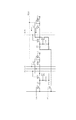
(列駆動回路)
本発明に用いられる列駆動回路を図4に示す。
この回路は、特許文献1に記載されている列駆動回路と同じである。詳しい説明は上記特許文献1を参照されたい。
(Column drive circuit)
A column drive circuit used in the present invention is shown in FIG.
This circuit is the same as the column drive circuit described in
この駆動回路は一対の電圧電流変換回路からなり、それらの主要な動作を説明する。スイッチングトランジスタM6がオフ、スイッチングトランジスタM10がオンされて、電圧電流変換トランジスタM9のドレイン電流が出力線idataに出力される。この時、サンプリング信号SPAにより、スイッチングトランジスタM1がオンして、アナログ映像信号電圧VIDEOはもう一つの電圧電流変換トランジスタM3のゲート電圧として蓄えられる。これにより、トランジスタM3は所定のドレイン電流を流せる状態となる。 This drive circuit is composed of a pair of voltage-current conversion circuits, and their main operations will be described. The switching transistor M6 is turned off, the switching transistor M10 is turned on, and the drain current of the voltage-current conversion transistor M9 is output to the output line data. At this time, the switching transistor M1 is turned on by the sampling signal SPA, and the analog video signal voltage VIDEO is stored as the gate voltage of another voltage-current conversion transistor M3. As a result, the transistor M3 enters a state in which a predetermined drain current can flow.
次に、トランジスタM6がオン、トランジスタM10がオフとなり、トランジスタM3のドレイン電流が出力線idataに出力される。この時、再び、サンプリング信号SPBによりスイッチングトランジスタM7がオンして、取り込まれたアナログ映像信号電圧VIDEOはトランジスタM9のゲート電圧として蓄えられる。これによりトランジスタM9はドレイン電流を流せる状態となる。 Next, the transistor M6 is turned on, the transistor M10 is turned off, and the drain current of the transistor M3 is output to the output line data. At this time, the switching transistor M7 is turned on again by the sampling signal SPB, and the captured analog video signal voltage VIDEO is stored as the gate voltage of the transistor M9. As a result, the transistor M9 enters a state in which a drain current can flow.
以上の2つの動作は行走査期間毎に繰り返され、出力線idataには順次、アナログ信号電流が出力される。アナログ映像信号電圧VIDEOの実効振幅によるトランジスタM3のゲート及びトランジスタM9のゲートの書き込み電圧Vと、トランジスタM3及びM9の駆動係数βを各々A及びBとする。 The above two operations are repeated for each row scanning period, and analog signal currents are sequentially output to the output line data. A write voltage V of the gate of the transistor M3 and the gate of the transistor M9 based on the effective amplitude of the analog video signal voltage VIDEO, and drive coefficients β of the transistors M3 and M9 are A and B, respectively.
トランジスタM3のドレイン電流i(M3)及びトランジスタM9のドレイン電流i(M9)は、以下の関係を満たす。
i(M3)=A×V2、
i(M9)=B×V2。
The drain current i (M3) of the transistor M3 and the drain current i (M9) of the transistor M9 satisfy the following relationship.
i (M3) = A × V 2 ,
i (M9) = B × V 2 .
各電圧電流変換回路の駆動係数は、容量C1(またはC3)とC2(またはC4)の容量分割比により決定される。また同時に電圧電流変換トランジスタM3(またはM9)のゲート長に対するゲート幅(W/L)によっても決定される。 The drive coefficient of each voltage-current conversion circuit is determined by the capacity division ratio of the capacitors C1 (or C3) and C2 (or C4). At the same time, it is determined by the gate width (W / L) with respect to the gate length of the voltage-current conversion transistor M3 (or M9).
各トランジスタに用いられる非単結晶半導体を活性層に用いたTFTは特性バラツキが大きいが、図4の回路構成では各列のトランジスタM3及びトランジスタM6の闘値電圧Vthの変動に基本的に影響されない。各列のトランジスタM3及びM6の駆動係数βの変動に対して影響は残るが、トランジスタM3及びM9のサイズを大きくすることで影響を低減できる。しかし、駆動係数βの変動に対して残った影響は、各列のデータ信号電流のバラツキとなり、該データ信号の電流量で表示輝度が決まるEL素子では表示画像に「縦筋」のような表示不均一性が視認されてしまう。 A TFT using a non-single crystal semiconductor used for each transistor as an active layer has a large variation in characteristics, but the circuit configuration in FIG. 4 is basically unaffected by fluctuations in the threshold voltage Vth of the transistors M3 and M6 in each column. . Although the influence remains on the variation of the drive coefficient β of the transistors M3 and M6 in each column, the influence can be reduced by increasing the sizes of the transistors M3 and M9. However, the remaining effect on the variation of the drive coefficient β is a variation in the data signal current of each column, and an EL element whose display luminance is determined by the current amount of the data signal displays a display such as “vertical stripe” on the display image. The non-uniformity will be visible.
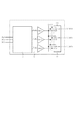
図5は表示画像に現れる「縦筋」を軽減する為の機能を含んだ列駆動回路3及び第2の選択回路の構成を示すものである。
FIG. 5 shows the configuration of the
図5はカラー表示装置に対応しており、RGB3に対応した3列の構成を示している。サンプリング信号SPA及びSPBは列電流発生回路1に入力される。
FIG. 5 corresponds to a color display device, and shows a three-row configuration corresponding to RGB3. Sampling signals SPA and SPB are input to the column
入力されるアナログ映像信号電圧VIDEO1は駆動係数A1及びB1をもつ電圧電流変換回路(上記図4と同じ一対の電圧電流変換回路)に入力される。入力されるアナログ映像信号電圧VIDEO2は駆動係数A2及びB2をもつ電圧電流変換回路(上記図4と同じ一対の電圧電流変換回路)に入力される。入力されるアナログ映像信号電圧VIDEO3は駆動係数A3及びB3をもつ電圧電流変換回路(上記図4と同じ一対の電圧電流変換回路)に入力される。 The input analog video signal voltage VIDEO1 is input to a voltage-current conversion circuit (the same pair of voltage-current conversion circuits as in FIG. 4) having drive coefficients A1 and B1. The input analog video signal voltage VIDEO2 is input to a voltage-current conversion circuit (the same pair of voltage-current conversion circuits as in FIG. 4) having drive coefficients A2 and B2. The input analog video signal voltage VIDEO3 is input to a voltage-current conversion circuit (the same pair of voltage-current conversion circuits as in FIG. 4) having drive coefficients A3 and B3.
3つの列駆動回路1の3つ出力線は3つの3入力1出力スイッチを含む分散スイッチ部(第2の選択回路)34に入力され、各々対応するR列、G列、B列にデータ信号電流iR、iG、iBとして出力される。
Three output lines of the three
分散スイッチ部34は、列駆動回路からデータ信号の出力先となるデータ線14を変更可能に選択する。制御線Ps2に制御回路35から供給される制御信号により、分散スイッチ部34の接続状態を変更可能に決定することができる。
The
そして、分散スイッチ部34の3つのスイッチは連動するように制御線Ps2に供給される制御信号により制御される。
The three switches of the distributed
図6は本発明に用いられる信号処理回路32を示す。図6の12は、入力されるデジタル映像データPIC1、PIC2、PIC3を表示パネル100で表示を行うためのデジタル映像信号に変換するデジタル信号処理するDSPである。DSP12から出力された表示パネルの画素構成に対応するデジタル映像信号は、赤色のデジタル映像信号Rdat、緑色のデジタル映像信号Gdat、青色のデジタル映像信号Bdatからなる。
FIG. 6 shows a
これらの色毎のデジタル映像信号は夫々デジタル・アナログ変換器DAC1、DAC2、DAC3で色毎のアナログ映像信号に変換され、マトリクス配線部を介して第1の選択回路である分散スイッチ部13に入力される。
These digital video signals for each color are converted into analog video signals for each color by the digital / analog converters DAC1, DAC2, and DAC3, respectively, and input to the
分散スイッチ部13は、制御線Ps1に入力される制御信号により、各DACの出力先であるアナログ映像信号ラインVIDEO1、VIDEO2、VIDEO3が適宜選択される。
The
制御線Ps1に供給される制御信号は信号処理回路13内部に集積化されている不図示の制御回路で生成される。制御線Ps1の制御信号によって、分散スイッチ部13の接続状態、つまりDACの出力先をどのアナログ映像信号ラインVIDEO1、VIDEO2、VIDEO3とするかを決定することができる。そして、この接続状態は変更可能である。
A control signal supplied to the control line Ps1 is generated by a control circuit (not shown) integrated in the
そして、第1の選択回路34と第2の選択回路13とは、協働して後述する適切な接続状態を選択するように、信号処理回路32内の制御回路13や制御回路35により制御される。
The
(比較例)
ここで、本発明の実施形態による作用効果を容易に理解しやすくするために、比較例について先に説明する。
(Comparative example)
Here, in order to easily understand the operational effects of the embodiment of the present invention, a comparative example will be described first.
列駆動回路及び選択回路として図5に示した構成を採用し、信号処理回路として、図7に示した構成を採用した場合について説明する。図7は信号処理回路の一例を示す。この回路は単結晶シリコンを用いたトランジスタの集積回路からなるLSIで構成される。 A case will be described in which the configuration shown in FIG. 5 is adopted as the column driving circuit and the selection circuit, and the configuration shown in FIG. 7 is adopted as the signal processing circuit. FIG. 7 shows an example of a signal processing circuit. This circuit is composed of an LSI composed of an integrated circuit of transistors using single crystal silicon.
入力されたデジタル映像データPIC1、PIC2、PIC3はDSP12に入力される。デジタル映像データPIC1、PIC2、PIC3はRGBデータ又はYUVデータでありうる。映像信号処理を行うDSP12ではデジタル映像データPIC1、PIC2、PIC3から表示装置に対応した色毎のデジタル映像信号Rdat、Gdat、Bdatを出力する。
The input digital video data PIC1, PIC2, and PIC3 are input to the
そのために、DSP12では、必要に応じて色空間変換(入力されるデジタル映像信号がRGBデータのときは不要)を行う。他にもDSP12では、解像度変換、輪郭強調、ノイズリダクション、ガンマ補正、ホワイトバランス、黒設定、輝度設定等から選択される少なくとも1種の処理がデジタル信号処理で行なわれる。
For this purpose, the
色毎のデジタル映像信号Rdat、Gdat、Bdatは、分散スイッチ部13を介して、それぞれゲインkのDAC1、DAC2、DAC3のいずれかに入力される。そして、DAC1、DAC2、DAC3からアナログ映像信号VIDEO1、VIDEO2、VIDEO3に変換されて出力される。
The digital video signals Rdat, Gdat, and Bdat for each color are input to any one of DAC1, DAC2, and DAC3 having a gain k through the
図5の列駆動回路と図7の表示装置制御回路から行なわれるRGB各表示に対応するための信号電流の発生動作を説明する。 An operation of generating signal currents corresponding to each RGB display performed from the column drive circuit of FIG. 5 and the display device control circuit of FIG. 7 will be described.
図7の分散スイッチ部13によって各DACに入力される各色データを下表1に示す。状態(1)から(3)は分散スイッチ部13の3つの接続状態に対応している。
The color data input to each DAC by the distributed

一方、図5の分散スイッチ部34によって選択された列駆動回路の駆動係数を示す。ここで、図4に示した列駆動回路では、先の水平走査期間でアナログ映像信号をサンプリングし、次の水平走査期間で先にサンプリングしたアナログ映像信号を電圧電流変換したデータ信号電流を供給する。よって、下表2に分散スイッチ部13の状態を対応させるとすると、上から(3)(1)(2)(3)(1)(2)の順になる。
On the other hand, the drive coefficient of the column drive circuit selected by the distributed
上述したとおり、図4の列駆動回路回路から出力される電流は1水平走査期間前に入力されたアナログ映像信号で決定されるので、表1及び表2からわかるように分散スイッチ部34、13の全ての選択状態においてRGB列のデータ線に所望色の信号電流が供給される。
As described above, since the current output from the column drive circuit circuit of FIG. 4 is determined by the analog video signal input before one horizontal scanning period, as can be seen from Tables 1 and 2, the
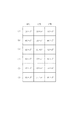
図8は列駆動回路の1式及び2式で示す電圧電流変換特性に従った各画素に対応する電圧電流変換係数を示した表である。 FIG. 8 is a table showing voltage-current conversion coefficients corresponding to the respective pixels according to the voltage-current conversion characteristics shown in the first and second formulas of the column drive circuit.
図8の左端にある数字は分散スイッチ部34、13の接続状態であり、各行で「(1)→(2)→(3)」を繰り返す。各列のデータ信号電流とも列駆動回路1内の駆動係数A1、B2、A3、B1、A2、B3の電圧電流変換回路を順次切り換えて出力している。よって、図8に示すように、駆動係数A1、B2、A3、B1、A2、B3間にバラツキが存在しても6行周期で分散されるので、表示画像の「縦筋」が視覚上低減される。
The numbers at the left end of FIG. 8 are the connection states of the distributed
しかしながら、図7のデジタル・アナログ変換器DAC1、DAC2、DAC3の各ゲインにはバラツキがある。これはLSI製造時に生じるトランジスタや内蔵抵抗器の特性ばらつきに因るものである。デジタル・アナログ変換器DAC1、DAC2、DAC3の各ゲインは、全て同一でなく、各々ゲインk1、k2、k3という互いに相違する値を持っている。 However, the gains of the digital / analog converters DAC1, DAC2, and DAC3 in FIG. 7 vary. This is due to variations in characteristics of transistors and built-in resistors that occur during LSI manufacturing. The gains of the digital / analog converters DAC1, DAC2, and DAC3 are not all the same, and have different values of gains k1, k2, and k3, respectively.
図9はこの場合の列駆動回路の1式及び2式で示す電圧電流変換特性に従った各画素に対応する電圧電流変換係数を示した表である。 FIG. 9 is a table showing voltage-current conversion coefficients corresponding to the respective pixels according to the voltage-current conversion characteristics shown in the first and second formulas of the column driving circuit in this case.
図9から理解できる様に、DAC1、DAC2、DAC3のゲインバラツキによって、各画素の電流が3行周期で変動してしまう。しかも、ゲインバラツキは2乗特性で強調されてしまう。このため表示画像全域に渡って、3行毎の繰り返し固定パターンの表示不均一性が発生してしまう。このゲインばらつきの2乗効果が、本発明者が見出した表示不均一性の一つの原因である。 As can be understood from FIG. 9, the current of each pixel fluctuates in a three-row cycle due to the gain variation of DAC1, DAC2, and DAC3. Moreover, the gain variation is emphasized by the square characteristic. For this reason, display nonuniformity of the repeated fixed pattern every three rows occurs over the entire display image. This square effect of gain variation is one cause of display non-uniformity found by the present inventors.
(実施形態1)
そこで、本発明は図1乃至6に示した構成のカラー表示装置により上記技術課題を解決する。図1の構成が、図7に示した構成と基本的に異なる点は、第1の選択回路である分散スイッチ部13とDACの位置が映像信号の流れに対して逆になっている点である。
(Embodiment 1)
Therefore, the present invention solves the above technical problem by the color display device having the configuration shown in FIGS. The configuration of FIG. 1 is fundamentally different from the configuration shown in FIG. 7 in that the positions of the
図1の分散スイッチ部13によって映像信号出力VIDEO1、VIDEO2、VIDEO3に出力される色信号を分散スイッチ部13の各接続状態で示す。
The color signals output to the video signal outputs VIDEO1, VIDEO2, and VIDEO3 by the distributed
図7の構成を採用した場合と同様に表3及び表2からわかるように分散スイッチ部34、13の全ての選択状態においてRGB列のデータ線に所望色のデータ信号電流が供給される。図10は列電流発生回路の1式及び2式で示す電圧電流変換特性に従った各画素に対応する電圧電流変換係数を示した表である。
As in the case of adopting the configuration of FIG. 7, as can be seen from Tables 3 and 2, a data signal current of a desired color is supplied to the data lines of the RGB columns in all selection states of the
図10の左端にある数字は分散スイッチ部34、13の接続状態であり、各行で「(1)→(2)→(3)」を繰り返す。各列の電流とも列駆動回路の駆動係数A1、B2、A3、B1、A2、B3の電圧電流変換回路を順次変更しながら発生させる。よって、図10からわかるよう駆動係数A1、B2、A3、B1、A2、B3間にバラツキが存在しても6行周期で分散される。しかも、各色列に供給されるデータ信号電流は同一のデジタル・アナログ変換器DACから来たアナログ映像信号に基づくものである。
The numbers at the left end of FIG. 10 are the connection states of the distributed
ゆえに、DAC1、DAC2、DAC3のゲインバラツキによる、3行毎の固定パターンの表示不均一性は発生しない。 Therefore, there is no display non-uniformity of the fixed pattern every three lines due to the gain variation of DAC1, DAC2, and DAC3.
確かに、DAC1、DAC2、DAC3のゲインバラツキによって、ホワイトバランスはズレるが、ホワイトバランスはDSP12において周知の方法によりデジタル処理で容易に調整可能である。
Certainly, the white balance shifts due to the gain variations of DAC1, DAC2, and DAC3, but the white balance can be easily adjusted by digital processing in the
したがって、図6の信号処理回路を使用すると図4に示した電圧電流変換回路の駆動係数A1、B2、A3、B1、A2、B3バラツキを表示画質に極力現れないように有効に分散できる。 Therefore, when the signal processing circuit shown in FIG. 6 is used, variations in driving coefficients A1, B2, A3, B1, A2, and B3 of the voltage-current conversion circuit shown in FIG. 4 can be effectively dispersed so as not to appear as much as possible in the display image quality.
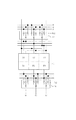
(実施形態2)
図11と図12は本実施の形態に用いられる第1及び第2の選択回路、列駆動回路、及び信号処理回路を示している。
(Embodiment 2)
11 and 12 show the first and second selection circuits, the column drive circuit, and the signal processing circuit used in this embodiment.
図12の信号処理回路には、第1の選択回路を設けずに、表示部と同じ絶縁性表面を有する基板上に、列駆動回路、第2の選択回路とともに第1の選択回路13が集積化されて設けられている。これらの回路のトランジスタは何れも多結晶シリコンなどの非単結晶半導体を活性層に用いたTFTで構成される。
In the signal processing circuit of FIG. 12, the
図12に示すように、DSP12からDAC1、DAC2、DAC3を介して各々R信号、G信号、B信号が並列に出力される。分散スイッチ部13は図11で示すように、列駆動回路や第2の選択回路34とともに集積化されている。図12ではDSP12とデジタル・アナログ変換器のみが、単結晶半導体基板に集積化され、1チップLSIとなっている。
As shown in FIG. 12, the R signal, the G signal, and the B signal are output in parallel from the
図11に示すように、第1の選択回路である分散スイッチ部13によって色毎のアナログ映像信号RGBは水平走査毎に接続状態が変更され、出力先の列駆動回路が変更される。しかしながら、第2の選択スイッチ34により、列駆動回路からのデータ信号電流の出力先が変更されるため、色毎のデータ信号電流は、対応する色のデータ線(iR,iG,iB)に供給される。
これら第1及び第2の選択回路は制御線Ps1及びPs2により制御される。
As shown in FIG. 11, the connection state of the analog video signal RGB for each color is changed every horizontal scanning by the
These first and second selection circuits are controlled by control lines Ps1 and Ps2.
実施形態1と同様に表3及び表2からわかるように分散スイッチ部34、13の全ての選択状態においてRGB列のデータ線に所望色のデータ信号電流が供給される。
As can be seen from Tables 3 and 2 in the same manner as in the first embodiment, a data signal current of a desired color is supplied to the RGB data lines in all selection states of the
図10に示すように各画素に対する電圧電流変換係数の分散状態は同じである。分散スイッチ部13は表示パネル上に表示画面の横サイズ全幅に亘って配置できるので分散スイッチ部13内の各スイッチの導通抵抗バラツキは極力抑えることができる。そして、各列駆動回路におけるサンプリング時定数に影響されるサンプリング動作のバランスがとれる。
As shown in FIG. 10, the dispersion state of the voltage-current conversion coefficient for each pixel is the same. Since the
また、図11ではデータ線一列に対して1つの分散用のスイッチを設けているが、複数のデータ線群に対して一つのスイッチを設けることも好ましい。このように、第1の選択回路のスイッチの数を列の数より少ない数にすることにより、RGBの各アナログ映像信号線マトリクス配線部の寄生容量を低減できる。また、選択回路13と列駆動回路1との間のマトリクス配線部における寄生容量も低減できる。更には、スイッチ部13自体のゲートの配線交差によって発生する寄生容量増加を抑えることもできる。こうして、サンプリング時定数が抑えられ、サンプリング動作のバランスが良くなる。
In FIG. 11, one distribution switch is provided for one line of data lines, but it is also preferable to provide one switch for a plurality of data line groups. Thus, by setting the number of switches of the first selection circuit to be smaller than the number of columns, the parasitic capacitance of each analog video signal line matrix wiring portion of RGB can be reduced. Further, the parasitic capacitance in the matrix wiring portion between the
また、実施形態1と同様に電圧電流変換回路の駆動係数A1、B2、A3、B1、A2、B3のバラツキが表示画質に極力現れないようにすることもできることは云うまでも無い。 Needless to say, as in the first embodiment, variations in the drive coefficients A1, B2, A3, B1, A2, and B3 of the voltage-current conversion circuit can be minimized in the display image quality.
1 列駆動回路
2 画素回路(色画素)
9 カラー表示部(マトリクス部)
13 第1の選択回路
14 データ線
32 信号処理回路
34 第2の選択回路
35 制御回路
Ps1、Ps2 制御線
1
9 Color display (matrix)
13
Claims (6)
前記カラー表示部に列毎に共通に接続された複数のデータ線と、
前記カラー表示部の列に対応して設けられ、前記画素に供給されるデータ信号を前記複数のデータ線に行毎に出力する複数の列駆動回路と、
を有するカラー表示装置において、
デジタル映像信号を色毎に各々DA変換して得られた色毎のアナログ映像信号の出力先となる前記列駆動回路を選択するための第1の選択回路と、
前記列駆動回路からの前記データ信号の出力先となる前記データ線を選択するための第2の選択回路と、
前記色毎のアナログ映像信号の出力先となる前記駆動回路と前記データ信号の出力先となる前記データ線とを走査期間毎に順次変更するように、前記第1及び第2の選択回路を制御する制御回路と、
を有することを特徴とするカラー表示装置。 A color display unit in which pixels having a plurality of electro-optic elements are arranged in a matrix;
A plurality of data lines commonly connected to the color display section for each column;
A plurality of column driving circuits which are provided corresponding to the columns of the color display unit and which output data signals supplied to the pixels to the plurality of data lines for each row;
In a color display device having
A first selection circuit for selecting the column drive circuit that is an output destination of the analog video signal for each color obtained by performing DA conversion on each digital video signal;
A second selection circuit for selecting the data line that is the output destination of the data signal from the column drive circuit;
The first and second selection circuits are controlled so as to sequentially change the drive circuit serving as the output destination of the analog video signal for each color and the data line serving as the output destination of the data signal for each scanning period. A control circuit to
A color display device comprising:
前記マトリクス部に列毎に共通に接続された複数のデータ線と、
前記マトリクス部の列に対応して設けられ、前記画素回路に供給されるデータ信号を前記複数のデータ線に行毎に出力する複数の列駆動回路と、
を有するアクティブマトリクス装置において、
デジタル映像信号を色毎に各々DA変換して得られた色毎のアナログ映像信号の出力先となる前記列駆動回路を選択するための第1の選択回路と、
前記列駆動回路からの前記データ信号の出力先となる前記データ線を選択するための第2の選択回路と、
前記色毎のアナログ映像信号の出力先となる前記駆動回路と前記データ信号の出力先となる前記データ線とを走査期間毎に順次変更するように、前記第1及び第2の選択回路を制御する制御線と、
を有することを特徴とするアクティブマトリクス装置。
A matrix portion in which a plurality of pixel circuits are arranged in a matrix;
A plurality of data lines commonly connected to the matrix portion for each column;
A plurality of column driving circuits which are provided corresponding to the columns of the matrix portion and output data signals supplied to the pixel circuits to the plurality of data lines for each row;
In an active matrix device having:
A first selection circuit for selecting the column drive circuit that is an output destination of the analog video signal for each color obtained by performing DA conversion on each digital video signal;
A second selection circuit for selecting the data line that is the output destination of the data signal from the column drive circuit;
The first and second selection circuits are controlled so as to sequentially change the drive circuit serving as the output destination of the analog video signal for each color and the data line serving as the output destination of the data signal for each scanning period. A control line to
An active matrix device comprising:
Priority Applications (3)
| Application Number | Priority Date | Filing Date | Title |
|---|---|---|---|
| JP2006097998A JP2007271969A (en) | 2006-03-31 | 2006-03-31 | Color display device and active matrix device |
| US12/063,306 US8305325B2 (en) | 2006-03-31 | 2007-03-30 | Color display apparatus and active matrix apparatus |
| PCT/JP2007/057690 WO2007114500A1 (en) | 2006-03-31 | 2007-03-30 | Data line driving circuit for colour active matrix display |
Applications Claiming Priority (1)
| Application Number | Priority Date | Filing Date | Title |
|---|---|---|---|
| JP2006097998A JP2007271969A (en) | 2006-03-31 | 2006-03-31 | Color display device and active matrix device |
Publications (2)
| Publication Number | Publication Date |
|---|---|
| JP2007271969A true JP2007271969A (en) | 2007-10-18 |
| JP2007271969A5 JP2007271969A5 (en) | 2009-05-14 |
Family
ID=38051689
Family Applications (1)
| Application Number | Title | Priority Date | Filing Date |
|---|---|---|---|
| JP2006097998A Pending JP2007271969A (en) | 2006-03-31 | 2006-03-31 | Color display device and active matrix device |
Country Status (3)
| Country | Link |
|---|---|
| US (1) | US8305325B2 (en) |
| JP (1) | JP2007271969A (en) |
| WO (1) | WO2007114500A1 (en) |
Families Citing this family (12)
| Publication number | Priority date | Publication date | Assignee | Title |
|---|---|---|---|---|
| US7608861B2 (en) * | 2004-06-24 | 2009-10-27 | Canon Kabushiki Kaisha | Active matrix type display having two transistors of opposite conductivity acting as a single switch for the driving transistor of a display element |
| JP5495510B2 (en) * | 2007-06-19 | 2014-05-21 | キヤノン株式会社 | Display device and electronic apparatus using the same |
| JP2009014836A (en) * | 2007-07-02 | 2009-01-22 | Canon Inc | Active matrix type display and driving method therefor |
| CN101779229B (en) * | 2007-08-21 | 2012-11-07 | 佳能株式会社 | Display apparatus and drive method thereof |
| JP2009080272A (en) * | 2007-09-26 | 2009-04-16 | Canon Inc | Active matrix type display device |
| JP2009109641A (en) * | 2007-10-29 | 2009-05-21 | Canon Inc | Driving circuit and active matrix type display device |
| JP2010008987A (en) * | 2008-06-30 | 2010-01-14 | Canon Inc | Drive circuit |
| JP2010122355A (en) * | 2008-11-18 | 2010-06-03 | Canon Inc | Display apparatus and camera |
| JP5284198B2 (en) * | 2009-06-30 | 2013-09-11 | キヤノン株式会社 | Display device and driving method thereof |
| JP2011013415A (en) * | 2009-07-01 | 2011-01-20 | Canon Inc | Active matrix type display apparatus |
| JP2011028135A (en) * | 2009-07-29 | 2011-02-10 | Canon Inc | Display device and driving method of the same |
| JP6124573B2 (en) | 2011-12-20 | 2017-05-10 | キヤノン株式会社 | Display device |
Citations (10)
| Publication number | Priority date | Publication date | Assignee | Title |
|---|---|---|---|---|
| JPH06222737A (en) * | 1993-01-21 | 1994-08-12 | Toshiba Corp | Driving circuit for display device |
| JPH0926765A (en) * | 1995-07-11 | 1997-01-28 | Texas Instr Japan Ltd | Signal line driving circuit for liquid crystal display |
| JPH09152850A (en) * | 1995-11-28 | 1997-06-10 | Victor Co Of Japan Ltd | Picture display device |
| JPH10260661A (en) * | 1997-03-19 | 1998-09-29 | Sharp Corp | Driving circuit for display device |
| JP2001242839A (en) * | 1999-12-24 | 2001-09-07 | Semiconductor Energy Lab Co Ltd | Semiconductor display device and electronics |
| JP2003157051A (en) * | 2001-09-04 | 2003-05-30 | Toshiba Corp | Display device |
| JP2003280616A (en) * | 2001-11-10 | 2003-10-02 | Lg Philips Lcd Co Ltd | Apparatus and method for driving data for liquid crystal display |
| JP2004145296A (en) * | 2002-09-02 | 2004-05-20 | Canon Inc | Current signal output circuit and display apparatus and information display apparatus using the current signal output circuit |
| JP2005164666A (en) * | 2003-11-28 | 2005-06-23 | Sanyo Electric Co Ltd | Driving system of display apparatus |
| JP2005301007A (en) * | 2004-04-14 | 2005-10-27 | Toppoly Optoelectronics Corp | Data driver and driving method |
Family Cites Families (15)
| Publication number | Priority date | Publication date | Assignee | Title |
|---|---|---|---|---|
| JP3529883B2 (en) | 1995-03-16 | 2004-05-24 | 株式会社東芝 | Signal converter |
| JP2001195042A (en) | 2000-01-05 | 2001-07-19 | Internatl Business Mach Corp <Ibm> | Source driver for liquid crystal panel and leveling method for source driver output variance |
| TW554558B (en) | 2001-07-16 | 2003-09-21 | Semiconductor Energy Lab | Light emitting device |
| KR100505773B1 (en) | 2001-08-22 | 2005-08-03 | 아사히 가세이 마이크로시스템 가부시끼가이샤 | Display panel drive circuit |
| JP2004094058A (en) * | 2002-09-02 | 2004-03-25 | Semiconductor Energy Lab Co Ltd | Liquid crystal display and its driving method |
| JP3950845B2 (en) | 2003-03-07 | 2007-08-01 | キヤノン株式会社 | Driving circuit and evaluation method thereof |
| JP4838498B2 (en) | 2003-05-21 | 2011-12-14 | キヤノン株式会社 | Display device |
| JP2005115287A (en) * | 2003-10-10 | 2005-04-28 | Nec Electronics Corp | Circuit for driving display device and its driving method |
| JP4054794B2 (en) | 2003-12-04 | 2008-03-05 | キヤノン株式会社 | DRIVE DEVICE, DISPLAY DEVICE, AND RECORDING DEVICE |
| US7184098B2 (en) | 2004-02-19 | 2007-02-27 | Spatialight, Inc. | Cyclic data signal averaging system and method for use in video display systems |
| US7608861B2 (en) | 2004-06-24 | 2009-10-27 | Canon Kabushiki Kaisha | Active matrix type display having two transistors of opposite conductivity acting as a single switch for the driving transistor of a display element |
| JP4438066B2 (en) | 2004-11-26 | 2010-03-24 | キヤノン株式会社 | Active matrix display device and current programming method thereof |
| JP4438067B2 (en) | 2004-11-26 | 2010-03-24 | キヤノン株式会社 | Active matrix display device and current programming method thereof |
| JP4438069B2 (en) | 2004-12-03 | 2010-03-24 | キヤノン株式会社 | Current programming device, active matrix display device, and current programming method thereof |
| US7872617B2 (en) | 2005-10-12 | 2011-01-18 | Canon Kabushiki Kaisha | Display apparatus and method for driving the same |
-
2006
- 2006-03-31 JP JP2006097998A patent/JP2007271969A/en active Pending
-
2007
- 2007-03-30 WO PCT/JP2007/057690 patent/WO2007114500A1/en active Application Filing
- 2007-03-30 US US12/063,306 patent/US8305325B2/en not_active Expired - Fee Related
Patent Citations (10)
| Publication number | Priority date | Publication date | Assignee | Title |
|---|---|---|---|---|
| JPH06222737A (en) * | 1993-01-21 | 1994-08-12 | Toshiba Corp | Driving circuit for display device |
| JPH0926765A (en) * | 1995-07-11 | 1997-01-28 | Texas Instr Japan Ltd | Signal line driving circuit for liquid crystal display |
| JPH09152850A (en) * | 1995-11-28 | 1997-06-10 | Victor Co Of Japan Ltd | Picture display device |
| JPH10260661A (en) * | 1997-03-19 | 1998-09-29 | Sharp Corp | Driving circuit for display device |
| JP2001242839A (en) * | 1999-12-24 | 2001-09-07 | Semiconductor Energy Lab Co Ltd | Semiconductor display device and electronics |
| JP2003157051A (en) * | 2001-09-04 | 2003-05-30 | Toshiba Corp | Display device |
| JP2003280616A (en) * | 2001-11-10 | 2003-10-02 | Lg Philips Lcd Co Ltd | Apparatus and method for driving data for liquid crystal display |
| JP2004145296A (en) * | 2002-09-02 | 2004-05-20 | Canon Inc | Current signal output circuit and display apparatus and information display apparatus using the current signal output circuit |
| JP2005164666A (en) * | 2003-11-28 | 2005-06-23 | Sanyo Electric Co Ltd | Driving system of display apparatus |
| JP2005301007A (en) * | 2004-04-14 | 2005-10-27 | Toppoly Optoelectronics Corp | Data driver and driving method |
Also Published As
| Publication number | Publication date |
|---|---|
| US8305325B2 (en) | 2012-11-06 |
| US20090102853A1 (en) | 2009-04-23 |
| WO2007114500A1 (en) | 2007-10-11 |
Similar Documents
| Publication | Publication Date | Title |
|---|---|---|
| JP2007271969A (en) | Color display device and active matrix device | |
| US10867561B2 (en) | Display apparatus | |
| US8552655B2 (en) | Image display apparatus | |
| JP6248352B2 (en) | Organic EL display device and driving method | |
| KR100535286B1 (en) | Display device and driving mithod thereof | |
| KR100659155B1 (en) | Current feedback type amoled driving circuit | |
| JP6232590B2 (en) | Display device and display method | |
| US11651720B2 (en) | Display device, method of driving display device, and electronic apparatus | |
| JP2010266848A (en) | El display device and driving method thereof | |
| JP2016009156A (en) | Gate driver circuit and el display device | |
| KR20190060909A (en) | Organic light emitting display device and method for driving thereof | |
| US20170316742A1 (en) | Data driver, display device, and electronic apparatus | |
| JP2007133351A (en) | Display unit, active matrix device, and driving method thereof | |
| KR20220084602A (en) | Electroluminescent Display Device And Driving Method Of The Same | |
| TW201220278A (en) | Organic light emitting diode displays | |
| WO2021111744A1 (en) | Electro-optical device, electronic equipment, and driving method | |
| CN111316345B (en) | Sub-pixel circuit, active type electroluminescent display and driving method thereof | |
| JP7344068B2 (en) | display device | |
| JP2012088550A (en) | Image display device and its control method | |
| TWI834387B (en) | Driving circuit for led panel and led panel thereof | |
| JP2015197477A (en) | Signal processing method, display device, and electronic apparatus | |
| KR102185118B1 (en) | Organic light emitting display and driving method thereof | |
| JP2005316110A (en) | Organic el display device and electronic apparatus | |
| US20150070377A1 (en) | Image signal processing circuit, image signal processing method and display apparatus | |
| US20190385539A1 (en) | Systems and methods of multiple color driving |
Legal Events
| Date | Code | Title | Description |
|---|---|---|---|
| A521 | Request for written amendment filed |
Free format text: JAPANESE INTERMEDIATE CODE: A523 Effective date: 20090331 |
|
| A621 | Written request for application examination |
Free format text: JAPANESE INTERMEDIATE CODE: A621 Effective date: 20090331 |
|
| RD04 | Notification of resignation of power of attorney |
Free format text: JAPANESE INTERMEDIATE CODE: A7424 Effective date: 20100201 |
|
| RD01 | Notification of change of attorney |
Free format text: JAPANESE INTERMEDIATE CODE: A7421 Effective date: 20100630 |
|
| A131 | Notification of reasons for refusal |
Free format text: JAPANESE INTERMEDIATE CODE: A131 Effective date: 20111108 |
|
| A02 | Decision of refusal |
Free format text: JAPANESE INTERMEDIATE CODE: A02 Effective date: 20120228 |