JP2007121368A - Liquid crystal device, and electronic device - Google Patents
Liquid crystal device, and electronic device Download PDFInfo
- Publication number
- JP2007121368A JP2007121368A JP2005309423A JP2005309423A JP2007121368A JP 2007121368 A JP2007121368 A JP 2007121368A JP 2005309423 A JP2005309423 A JP 2005309423A JP 2005309423 A JP2005309423 A JP 2005309423A JP 2007121368 A JP2007121368 A JP 2007121368A
- Authority
- JP
- Japan
- Prior art keywords
- liquid crystal
- display
- sub
- pixels
- display area
- Prior art date
- Legal status (The legal status is an assumption and is not a legal conclusion. Google has not performed a legal analysis and makes no representation as to the accuracy of the status listed.)
- Pending
Links
Images


Abstract
Description
本発明は、反射モードと透過モード、及び反射と透過の両方の表示を行う透過反射兼用
モードを備えた液晶装置、及び電子機器に関する。
The present invention relates to a liquid crystal device having a reflection mode and a transmission mode, and a transmission / reflection mode for performing both reflection and transmission, and an electronic apparatus.
近年、携帯電話やPDA等の表示装置として、反射モードと透過モードの双方を備えた
半透過反射型の液晶装置が広く使用されている。このような半透過反射型液晶装置として
は、アルミニウム等の金属膜に光透過用のスリット(開口部)を形成した反射膜を下基板
の内面に備え、この反射膜を半透過反射膜として機能させるものが知られている。この場
合、反射モードでは、上基板側から入射した外光が、液晶層を通過した後に下基板の内面
の反射膜で反射され、再び液晶層を通過して上基板側から射出され、表示に寄与する。一
方、透過モードでは下基板側から入射したバックライトからの光が、反射膜の開口部から
液晶層を通過した後、上基板側から外部に射出され、表示に寄与する。したがって、反射
膜の形成領域のうち、開口部が形成された領域が透過表示領域、その他の領域が反射表示
領域となる(特許文献1参照)。
このような半透過反射型の液晶装置としては、上基板又は下基板のいずれかにカラーフ
ィルタを設けたものが広く使用されている。例えば、先の特許文献1には、カラーフィル
タを透過表示領域(反射膜の開口部)のみに設けた液晶装置が開示されており、反射モー
ドをカラー表示とせずに、白黒表示として明るさを稼いでいる。
As such a transflective liquid crystal device, a liquid crystal device in which a color filter is provided on either an upper substrate or a lower substrate is widely used. For example,
しかしながら、上記の液晶装置では、1つのサブ画素(サブピクセル)に透過表示領域
と反射表示領域とを設けている。そのため、(1)透過カラー表示に反射表示のモノクロ
成分が混じることによる表示品位の低下、(2)反射モノクロ表示に透過表示領域からの
反射光が混じることによる表示品位の低下、(3)反射表示領域及び透過表示領域のみの
液晶駆動ができないため、表示に寄与しないサブピクセルを駆動することによる消費電力
の浪費、等の問題が生じ得る。
However, in the above-described liquid crystal device, a transmissive display area and a reflective display area are provided in one subpixel (subpixel). Therefore, (1) the display quality is reduced due to the mixture of the monochrome component of the reflective display in the transmissive color display, (2) the display quality is deteriorated due to the reflected monochrome display mixed with the reflected light from the transmissive display area, and (3) the reflection. Since the liquid crystal cannot be driven only in the display area and the transmissive display area, problems such as waste of power consumption due to driving sub-pixels that do not contribute to display may occur.
本発明はこのような事情に鑑みてなされたもので、外光の状態に応じて最適な表示モー
ドの選択が可能で、透過モードにおいては鮮やかなカラー表示が可能であり、反射モード
においては明るいモノカラー表示又はモノクロ表示が可能であるとともに、消費電力の低
減も実現可能な液晶装置、及びこれを備えた電子機器を提供することを目的としている。
The present invention has been made in view of such circumstances, and it is possible to select an optimal display mode according to the state of external light, vivid color display is possible in the transmissive mode, and bright in the reflective mode. It is an object of the present invention to provide a liquid crystal device capable of monochromatic display or monochrome display and also capable of reducing power consumption, and an electronic apparatus including the liquid crystal device.
上記の課題を解決するため、本発明の液晶装置は、一対の基板間に液晶層を挟持してな
る液晶パネルを具備した液晶装置であって、各々が異なる色に対応した複数のサブ画素か
らなる画素を備え、前記画素の各々には、透過表示を行う透過表示領域と、反射表示を行
う反射表示領域とが配設されてなり、前記透過表示領域は複数の前記サブ画素から構成さ
れる一方、前記反射表示領域は前記透過表示領域とは別個の前記サブ画素から構成されて
なることを特徴とする。
In order to solve the above problems, a liquid crystal device of the present invention is a liquid crystal device including a liquid crystal panel in which a liquid crystal layer is sandwiched between a pair of substrates, each of which includes a plurality of subpixels corresponding to different colors. Each of the pixels is provided with a transmissive display area for performing transmissive display and a reflective display area for performing reflective display, and the transmissive display area includes a plurality of the sub-pixels. On the other hand, the reflective display area is composed of the sub-pixels separate from the transmissive display area.
このような液晶装置によると、透過表示領域と反射表示領域をそれぞれ別個のサブ画素
で構成しているため、透過と反射の表示を別個に最適条件で行うことが可能となる。また
、従来のように透過表示領域と反射表示領域とを同一のサブ画素内に配設する場合とは異
なり、各表示領域を別個のサブ画素で構成しているため、当該各表示領域のサブ画素構造
を任意に最適化することができ、透過及び反射の各表示についてそれぞれ光学特性の最適
化を図ることが可能となる。さらに、各表示領域を別個のサブ画素で構成しているため、
透過又は反射のいずれか一方の表示モードの際には、一方の表示領域においてサブ画素を
駆動状態とし、他方の表示領域においてサブ画素を非駆動状態とすれば、消費電力の削減
を図ることが可能となる。また、透過モードと反射モードの切り換えを各サブ画素の駆動
により実現できるため、環境(外光の状態)に応じた透過と反射の表示切換が可能となる
。さらに、従来の特許文献1のような構成では、透過表示領域と反射表示領域とが同一の
サブ画素内に配置されることで混色の問題が生じたり、透過時に反射の光が視認され又は
反射時に透過の光が視認されてコントラストが低下したりする問題があるが、本発明では
各表示領域が別個のサブ画素を具備してなるため、そのような問題が悉く解決され、混色
防止さらには高コントラストの表示が実現されることとなる。
According to such a liquid crystal device, since the transmissive display area and the reflective display area are configured by separate sub-pixels, it is possible to perform transmissive and reflective display separately under optimum conditions. Further, unlike the conventional case where the transmissive display area and the reflective display area are arranged in the same subpixel, each display area is composed of separate subpixels. The pixel structure can be arbitrarily optimized, and the optical characteristics can be optimized for each of transmission and reflection displays. Furthermore, since each display area is composed of separate sub-pixels,
In one of the transmissive and reflective display modes, the power consumption can be reduced by setting the sub-pixel in the display state in one display region and in the non-drive state in the other display region. It becomes possible. In addition, since switching between the transmission mode and the reflection mode can be realized by driving each sub-pixel, it is possible to switch between transmission and reflection display according to the environment (state of external light). Further, in the configuration as in the
本発明の液晶装置において、前記透過表示領域ではフルカラー表示が行われる一方、前
記反射表示領域ではモノカラー表示又はモノクロ表示が行われるものとすることができる
。一般的に、透過表示ではバックライト(照明装置)を用いて表示を行い、反射表示では
外光を用いて表示を行う。したがって、透過表示は反射表示に比して表示特性が高く視認
性に優れている。そこで、本発明では、透過表示をフルカラー表示、反射表示をモノカラ
ー表示(単色表示)又はモノクロ表示(白黒表示)として表示の最適化を図っている。具
体的には、透過表示領域に、赤色の着色層が形成された赤色サブ画素と、緑色の着色層が
形成された緑色サブ画素と、青色の着色層が形成された青色サブ画素とを形成する一方、
反射表示領域に、無色透光性の樹脂層が形成されたモノクロサブ画素、又は所定の色の着
色層が形成されたモノカラーサブ画素を形成するものとすることができる。
In the liquid crystal device of the present invention, full-color display is performed in the transmissive display region, while mono-color display or monochrome display is performed in the reflective display region. In general, display is performed using a backlight (illumination device) in transmissive display, and display is performed using external light in reflective display. Accordingly, the transmissive display has higher display characteristics and better visibility than the reflective display. Therefore, in the present invention, the display is optimized by setting the transmissive display as a full color display and the reflective display as a monocolor display (monochrome display) or a monochrome display (monochrome display). Specifically, a red subpixel in which a red coloring layer is formed, a green subpixel in which a green coloring layer is formed, and a blue subpixel in which a blue coloring layer is formed are formed in the transmissive display area. While
A monochrome subpixel in which a colorless and translucent resin layer is formed or a monocolor subpixel in which a colored layer of a predetermined color is formed may be formed in the reflective display region.
また、本発明の液晶装置は、前記各サブ画素への注入電荷量を制御するソースドライバ
を有し、前記前記ソースドライバは、前記透過表示領域と前記反射表示領域の前記サブ画
素を駆動して透過表示と反射表示とを行う透過反射兼用モードと、前記透過表示領域に配
設されたサブ画素を駆動して透過表示を行う透過モードと、前記反射表示領域に配設され
たサブ画素を駆動して反射表示を行う反射モードとを選択可能に構成されているものとす
ることができる。このような構成によると、3つの駆動状態を環境(外光状態)に応じて
適宜選択することができるようになる。なお、透過反射兼用モードでは、暗い所では透過
が、明るい所では反射が視認される。
The liquid crystal device of the present invention further includes a source driver that controls the amount of charge injected into each subpixel, and the source driver drives the subpixels in the transmissive display area and the reflective display area. A transmissive / reflective mode for performing transmissive display and reflective display, a transmissive mode for performing transmissive display by driving sub-pixels arranged in the transmissive display area, and driving a sub-pixel arranged in the reflective display area Thus, the reflection mode for performing the reflection display can be selected. According to such a configuration, the three driving states can be appropriately selected according to the environment (external light state). In the transmission / reflection mode, transmission is visible in a dark place and reflection is visible in a bright place.
本発明の液晶装置において、前記液晶パネルの観察側とは反対側に、当該液晶パネルに
照明光を照射する照明装置が配設され、前記反射モードにおいて前記照明装置が消灯され
るものとすることができる。つまり、反射モード時は照明装置の照明光は不要なため、上
述のように照明装置を消灯すれば消費電力の低下に寄与することができ、また透過表示領
域からの漏光が視認される不具合発生も防止できることとなる。
In the liquid crystal device of the present invention, an illumination device that irradiates the liquid crystal panel with illumination light is disposed on the opposite side of the liquid crystal panel from the observation side, and the illumination device is turned off in the reflection mode. Can do. In other words, the illumination light of the illumination device is not necessary in the reflection mode, so if the illumination device is turned off as described above, it can contribute to a reduction in power consumption, and there is a problem that light leakage from the transmissive display area is visually recognized. Can also be prevented.
また、本発明の液晶装置は、前記反射モードにおいて、表示データを更新するリフレッ
シュレートが透過反射兼用モード又は前記透過モードよりも低くされているものとするこ
とができる。つまり、反射のモノカラー表示又はモノクロ表示では静止画や単調な動画表
示を採用することが多いため、リフレッシュレートを低くすることができるのである。
In the liquid crystal device of the present invention, the refresh rate for updating display data in the reflection mode may be lower than that in the transmission / reflection mode or the transmission mode. That is, in the reflective mono-color display or monochrome display, a still image or a monotone moving image display is often used, so that the refresh rate can be lowered.
さらに、前記反射モードにおいて、前記透過表示領域に配設されたサブ画素の表示が黒
表示とされるものとすることができる。反射モードにおいては透過表示が視認されないよ
うにすべきであり、上記のように反射モードで透過表示領域のサブ画素を黒表示とすれば
、表示上余分な光が混ざることを防止できるようになる。
一方、前記透過モードにおいて、前記反射表示領域に配設されたサブ画素の表示が黒表
示とされるものとすることができる。透過モードにおいては反射表示が視認されないよう
にすべきであり、上記のように透過モードで反射表示領域のサブ画素を黒表示とすれば、
表示上余分な光が混ざることを防止できるようになる。
なお、本発明の液晶装置において好ましくはノーマリブラックモードを採用するのが良
い。これにより非駆動状態のサブ画素を黒表示することができる。
Furthermore, in the reflection mode, the display of the sub-pixels disposed in the transmissive display area can be black. In the reflective mode, the transmissive display should not be visually recognized. If the sub-pixels in the transmissive display area are displayed in black in the reflective mode as described above, it is possible to prevent mixing of excess light on the display. .
On the other hand, in the transmissive mode, the display of the sub-pixels disposed in the reflective display area can be black. In the transmissive mode, the reflective display should not be visually recognized. As described above, if the sub-pixels in the reflective display area are displayed in black in the transmissive mode,
It is possible to prevent excessive light from being mixed on the display.
In the liquid crystal device of the present invention, a normally black mode is preferably adopted. As a result, the non-driven sub-pixel can be displayed in black.
また、本発明の液晶装置においては、前記ソースドライバの1つを用いて1つの画素内
の各サブ画素を時分割駆動するものとすることができる。この場合、透過反射兼用モード
では1つのソース出力で透過表示領域の各サブ画素と反射表示領域のサブ画素とを時分割
駆動し、透過モードでは1つのソース出力で透過表示領域の各サブ画素を時分割駆動し、
反射モードでは1つのソース出力で反射表示領域のサブ画素のみを時分割駆動することが
できる。このような時分割駆動の採用によりソースドライバの出力数を小さくすることが
できる。また、表示に寄与しないサブ画素を選択駆動しないことで、表示に寄与するサブ
画素へのデータ書き込みのマージンを広げることが可能となる。
In the liquid crystal device of the present invention, each of the sub-pixels in one pixel can be time-division driven using one of the source drivers. In this case, in the transmission / reflection combined mode, each subpixel of the transmissive display area and the subpixel of the reflective display area are time-division driven with one source output, and each subpixel of the transmissive display area is controlled with one source output in the transmissive mode. Time-sharing drive,
In the reflection mode, only the sub-pixels in the reflection display area can be time-division driven with one source output. By adopting such time division driving, the number of outputs of the source driver can be reduced. Further, by not selectively driving the sub-pixels that do not contribute to display, it is possible to widen the margin for data writing to the sub-pixels that contribute to display.
さらに、本発明の液晶装置において、前記一対の基板の少なくとも一方の基板の前記液
晶層側には、着色層を含むカラーフィルタ層が配設され、前記透過表示領域のカラーフィ
ルタ層には、前記各サブ画素毎に異なる色の着色層が配設される一方、前記反射表示領域
のカラーフィルタ層には、前記単一のサブ画素に着色層又は無色透光層が配設され、前記
反射表示領域の着色層又は無色透光層が前記透過表示領域の着色層よりも前記液晶層側に
突出形成されて、当該反射表示領域の液晶層厚が前記透過表示領域の液晶層厚よりも小さ
く構成されてなるものとすることができる。このように反射表示領域に配設された着色層
又は無色透光層を液晶層側に突出形成し、反射表示領域の液晶層厚を透過表示領域の液晶
層厚よりも小さく構成すれば、透過表示領域と反射表示領域とにおいてリタデーションの
均一化を図ることが可能となる。つまり、透過表示では照明装置から入射した光が液晶層
を1回通過して観察側に供される一方、反射表示では観察側から入射した外光が液晶層を
往復するため2回通過して観察側に供されるため、リタデーションの値が不均一となるが
、本発明のように着色層又は無色透光層を液晶層に突出形成することで当該リタデーショ
ン値の均一化を図ることができるのである。なお、反射表示領域における着色層又は無色
透光層の液晶層への突出量は、液晶層厚の半分に設計することが好ましい。
Furthermore, in the liquid crystal device of the present invention, a color filter layer including a colored layer is disposed on the liquid crystal layer side of at least one of the pair of substrates, and the color filter layer in the transmissive display region includes the color filter layer. A colored layer having a different color is provided for each sub-pixel, while a color layer or a colorless light-transmitting layer is provided for the single sub-pixel in the color filter layer of the reflective display region, and the reflective display A colored layer or a colorless light-transmitting layer in the region is formed so as to protrude toward the liquid crystal layer with respect to the colored layer in the transmissive display region, and the liquid crystal layer thickness in the reflective display region is smaller than the liquid crystal layer thickness in the transmissive display region It can be made. If a colored layer or a colorless light-transmitting layer arranged in the reflective display area is formed so as to protrude toward the liquid crystal layer and the thickness of the liquid crystal layer in the reflective display area is smaller than the liquid crystal layer thickness in the transmissive display area, It is possible to make the retardation uniform in the display area and the reflective display area. That is, in transmissive display, light incident from the illumination device passes through the liquid crystal layer once and is supplied to the observation side, whereas in reflective display, external light incident from the observation side passes through the liquid crystal layer and passes twice. Since it is provided on the observation side, the retardation value is non-uniform, but the retardation value can be made uniform by protruding the colored layer or the colorless light-transmitting layer on the liquid crystal layer as in the present invention. It is. In addition, it is preferable to design the protrusion amount to the liquid crystal layer of the colored layer or the colorless light-transmitting layer in the reflective display region to be half of the liquid crystal layer thickness.
また、本発明の液晶装置において、各サブ画素の面積が異なる構成としても良い。例え
ば反射表示を優先的に使うような場合には、反射表示領域のサブ画素の面積を大きくすれ
ば良い。また、反射表示領域におけるサブ画素の表示色については任意に選択可能である
が、省エネルギーで明るさを向上させるためには、好ましくは無色(白色)が好ましく、
この場合、透過表示に際して色付きが生じる等の問題も回避することができる。
In the liquid crystal device of the present invention, the sub pixels may have different areas. For example, when the reflective display is used preferentially, the area of the sub-pixels in the reflective display area may be increased. The display color of the sub-pixels in the reflective display area can be arbitrarily selected, but in order to improve the brightness with energy saving, it is preferably colorless (white),
In this case, it is possible to avoid problems such as coloring in transmissive display.
本発明の電子機器は、前述した本発明の液晶装置を備えたことを特徴とする。
これにより、透過モードにおいては鮮やかなカラー表示であり、反射モードにおいては
明るいモノカラー表示又はモノクロ表示が可能な表示部を備えた電子機器を提供すること
ができる。
An electronic apparatus according to the present invention includes the above-described liquid crystal device according to the present invention.
Accordingly, it is possible to provide an electronic device including a display unit that can display bright color in the transmissive mode and bright monochromatic or monochrome in the reflective mode.
以下、本発明の実施の形態を図面を用いて説明する。なお、各図においては、各層や各
部材を図面上で認識可能な程度の大きさとするため、各層や各部材毎に縮尺を異ならせて
ある。
Hereinafter, embodiments of the present invention will be described with reference to the drawings. In addition, in each figure, in order to make each layer and each member the size which can be recognized on drawing, the scale is varied for every layer and each member.
[液晶装置]
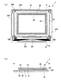
図1は、薄膜トランジスタを具備した液晶表示装置を示す全体平面図及び断面図であっ
て、本発明の液晶装置の一実施の形態に係るものである。つまり、図1(a)は、本実施
形態の液晶表示装置1を各構成要素とともに対向基板側からみた平面構成図、図1(b)
は、図1(a)に示すH−H線に沿う断面構成図、図2は、液晶装置の表示領域において
マトリクス状に配列形成された複数のサブ画素における回路構成図である。
[Liquid Crystal Device]
FIG. 1 is an overall plan view and a cross-sectional view showing a liquid crystal display device including a thin film transistor, and relates to an embodiment of the liquid crystal device of the present invention. That is, FIG. 1A is a plan configuration diagram of the liquid
FIG. 2 is a cross-sectional configuration diagram taken along line HH shown in FIG. 1A, and FIG. 2 is a circuit configuration diagram of a plurality of subpixels arranged in a matrix in the display region of the liquid crystal device.
図1(a)及び図1(b)に示すように、本実施形態の液晶表示装置1は、TFTアレ
イ基板(アクティブマトリクス基板)10と、対向基板20とが平面視略矩形枠状のシー
ル材52によって貼り合わされ、このシール材52に囲まれた領域内に液晶層50が封入
された構成を備えている。枠状のシール材52の内側には、その内周側に沿って平面視矩
形枠状の周辺見切り53が形成され、この周辺見切りの内側の領域が画像表示領域54と
されている。シール材52の外側の領域には、データ線駆動回路201及び外部回路実装
端子202がTFTアレイ基板10の1辺(図示下辺)に沿って形成されており、この1
辺に隣接する2辺に沿ってそれぞれ走査線駆動回路204,204が形成されている。T
FTアレイ基板10の残る1辺(図示上辺)には、画像表示領域11の両側の走査線駆動
回路204,204間を接続する複数の配線205が設けられている。
As shown in FIGS. 1A and 1B, the liquid
Scan
On the remaining one side (the upper side in the figure) of the
また、対向基板20の各角部においては、TFTアレイ基板10と対向基板20との間
の電気的導通をとるための基板間導通材206が配設されている。本実施形態の液晶表示
装置は、透過と反射の両表示が可能な液晶表示装置として構成されている。具体的に、透
過モードではTFTアレイ基板10側に配置された光源(図示略)からの光を液晶層50
で適宜変調して対向基板20側から出射するようになっている。一方、反射モードでは対
向基板20側からの光(外光等)を液晶層50において変調してTFTアレイ基板10上
に形成した反射膜13(図3参照)で反射させるとともに、当該反射光を再び液晶層50
で適宜変調して対向基板20側から出射するようになっている。
Further, an inter-substrate
Thus, the light is appropriately modulated and emitted from the
Thus, the light is appropriately modulated and emitted from the
なお、データ線駆動回路201および走査線駆動回路204,204をTFTアレイ基
板10の上に形成する代わりに、例えば、駆動用LSIが実装されたCOF(Chip On Fi
lm)基板とTFTアレイ基板10の周辺部に形成された端子群とを異方性導電膜を介して
電気的および機械的に接続するようにしてもよい。また、液晶表示装置においては、使用
する液晶の種類、すなわち、TN(Twisted Nematic)モード、STN(Super Twisted N
ematic)モード、垂直配向モード等の動作モードや、ノーマリホワイトモード/ノーマリ
ブラックモードの別に応じて、位相差板、偏光板等が所定の向きに配置されるが、ここで
は図示を省略する。
Instead of forming the data line driving
lm) The substrate and the terminal group formed on the periphery of the
ematic) mode, vertical alignment mode, and other modes, and a retardation plate, a polarizing plate, etc. are arranged in a predetermined direction depending on the normally white mode / normally black mode, but the illustration is omitted here. .
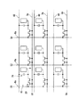
このような構造を有する液晶表示装置の画像表示領域には、図2に示すように、複数の
サブ画素41がマトリクス状に配置されており、これらのサブ画素41の各々には、画素
スイッチング用としてP型のp−SiTFT30が形成されている。このTFT30には
マルチゲート構造が採用されており、シングルゲート構造を採用したものに比べて、TF
T30の1つのTFTに印加されるドレイン−ソース間電圧を低減できるようになってい
る。このTFT30の複数のゲート電極には走査線3aが電気的に接続されており、走査
線3aから所定のタイミングでパルス状の走査信号G1、G2、・・・、Gmがこの順に
線順次で印加されるようになっている。また、TFT30のソース部にはデータ線6aが
電気的に接続されており、1走査期間内に画像信号S1、S2、・・・、Snが供給され
るようになっている。
In the image display area of the liquid crystal display device having such a structure, as shown in FIG. 2, a plurality of sub-pixels 41 are arranged in a matrix, and each of these sub-pixels 41 is provided for pixel switching. As a result, a p-type p-
The drain-source voltage applied to one TFT of T30 can be reduced. A
TFT30のドレイン部には画素電極9が電気的に接続されており、1走査期間内にデ
ータ線6aから供給される画像信号S1、S2、・・・、Snが各サブ画素に所定のタイ
ミングで書き込まれるようになっている。このようにして画素電極9を介して液晶に書き
込まれた所定レベルの画像信号S1、S2、・・・、Snは、図1(b)に示す対向基板
20の共通電極21との間で一定期間保持される。また、保持された画像信号S1、S2
、・・・、Snがリークするのを防ぐために、画素電極9と対向電極21との間に形成さ
れる液晶容量と並列に保持容量70が付加されている。
The
In order to prevent Sn from leaking, a
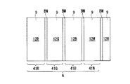
図3は、本実施形態の液晶表示装置を構成するTFTアレイ基板10上の1画素領域(
隣接画素領域を一部含む)の断面模式図であり、図4は、同じく1画素領域の平面模式図
である。なお、本実施形態では4つのサブ画素41(図3,4では符号41R,41G,
41B,41Wで示す)を1つのユニットとして1つの画素Aが構成されている。
TFTアレイ基板10には、図2に示したように、先述のデータ線6aと走査線3aと
が互いに交差して設けられ、これらのデータ線6aと走査線3aとによって区画された略
矩形状の領域によりサブ画素41が構成されている。そして、サブ画素41(41R,4
1G,41B,41W)と略重なる平面領域には、図3及び図4に示すように、ITO等
の透明導電材料からなる平面視矩形状の画素電極9が形成されている。
FIG. 3 shows one pixel region (on the
4 is a schematic plan view of one pixel region. In the present embodiment, four sub-pixels 41 (
41B and 41W) constitute one unit, and one pixel A is configured.
As shown in FIG. 2, the
1G, 41B, and 41W), a
ここで、本実施形態では各サブ画素41について、サブ画素41Rでは赤色の表示が、
サブ画素41Gでは緑色の表示が、サブ画素41Bでは青色の表示が、サブ画素41Wで
は白色の表示がそれぞれ可能とされている。また、サブ画素41R,41B,41Gは透
過表示領域Tを構成しており、サブ画素41Wは反射表示領域Rを構成している。したが
って、本実施形態の液晶表示装置1は、透過表示領域Tではフルカラー表示が、反射表示
領域Rではモノクロ表示が行われるものとなっている。なお、反射表示領域Rに単一の着
色層を配設して、当該反射表示領域Rをモノカラー表示可能な構成としても良い。
Here, in this embodiment, for each sub-pixel 41, the sub-pixel 41R displays red.
The sub-pixel 41G can display green, the sub-pixel 41B can display blue, and the sub-pixel 41W can display white. The sub-pixels 41R, 41B, and 41G constitute a transmissive display area T, and the sub-pixel 41W constitutes a reflective display area R. Therefore, in the liquid
次に、図3に示す断面構造において、TFTアレイ基板10は、例えば石英、ガラス、
プラスチック等からなる基板本体11の一面側に、下地絶縁膜(図示略)が形成され、こ
の下地絶縁膜上にTFT30(図3では図示省略)が設けられている。TFT30は、画
素電極9と接続されており、各画素電極9をスイッチング駆動できる構成とされている。
画素電極9は、各サブ画素41(41R,41G,41B,41W)毎にマトリクス状
に配設されている。なお、反射表示領域Rにおいては、基板本体11上にアルミニウム(
光反射性材料)からなる反射膜13が形成され、該反射膜13上に画素電極9が形成され
ている。また、TFTアレイ基板10の最表面には、ラビング処理等の配向処理が施され
たポリイミド膜等からなる配向膜16が設けられている。
Next, in the cross-sectional structure shown in FIG. 3, the
A base insulating film (not shown) is formed on one surface side of the
The
A
他方、対向基板20は、基板本体21の液晶層50側にカラーフィルタ12、平坦化膜
24、対向電極25、配向膜26を具備して構成されている。カラーフィルタ12は、画
素A毎に赤色着色層12R、緑色着色層12G、青色着色層12B、及び透光性樹脂層1
2Wを具備しており、各着色層12R,12G,12B,12WがブラックマトリクスB
Mにより区画構成されている。そして、赤色着色層12Rはサブ画素41Rに配設され、
緑色着色層12Gはサブ画素41G、青色着色層12Bはサブ画素41Gに配設されて各
サブ画素毎の色を創出しており、これら各色サブ画素を含む透過表示領域Tはフルカラー
表示が可能とされている。
On the other hand, the
2W, each
It is partitioned by M. The red
The green
また、透光性樹脂層12Wはサブ画素41Wに配設されて、反射表示領域Rのモノクロ
表示に寄与しており、且つ各着色層12R,12G,12Bよりも液晶層50側に突出す
る凸状部として構成されている。このように透光性樹脂層12Wを凸状部として構成する
ことで、当該反射表示領域Rにおける液晶層厚が透過表示領域Tにおける液晶層厚よりも
小さく構成されている。具体的には、反射表示領域Rの液晶層厚が透過表示領域Tの液晶
層厚の半分となるように、透光性樹脂層12Wの突出量が調整されている。なお、この場
合の透光性樹脂層12Wはアクリル樹脂よりなるものを採用している。
Further, the
次に、このようなカラーフィルタ12上には透光性樹脂からなる平坦化膜24を介して
対向電極(共通電極)25が基板全面ベタ状に配設されている。この場合の対向電極25
は、画素電極9と同様、ITO等の透光性導電材料から構成されている。なお、対向電極
25の液晶層50側には、先のTFTアレイ基板10の配向膜16と同様のポリイミド膜
からなる配向膜26が配設されている。
Next, on the
Like the
一方、一対の基板10,20間に液晶層50を挟持した構成の液晶パネル1aの内面側
、つまり当該液晶表示装置1の観察側とは異なる側にはバックライト(照明装置)40が
配設されている。液晶表示装置1では、このバックライト40からの光を利用して透過表
示が供され、観察側から入る外光等を利用して反射表示が供される。
On the other hand, a backlight (illumination device) 40 is disposed on the inner surface side of the
ここで、図1に示したデータ線駆動回路201は、各サブ画素41(41R,41G,
41B,41W)への注入電荷量を制御可能に構成されており、以下の3つの駆動モード
を選択可能とされている。
(1)全てのサブ画素41R,41G,41B,41Wを駆動して透過と反射との兼用
パネルとして動作する透過反射兼用モード。
(2)透過表示領域Tのサブ画素41R,41G,41Bを駆動して透過パネルとして
動作する透過モード。
(3)反射表示領域Rのサブ画素41Wを駆動して反射パネルとして動作する反射モー
ド。
なお、透過反射兼用モードでは、暗所で透過表示が供され、明所で反射表示が供される
。
Here, the data
41B, 41W), and the following three drive modes can be selected.
(1) A transmissive / reflective mode in which all the sub-pixels 41R, 41G, 41B, 41W are driven to operate as a transmissive / reflective panel.
(2) A transmissive mode in which the sub-pixels 41R, 41G, and 41B in the transmissive display area T are driven to operate as a transmissive panel.
(3) A reflection mode in which the sub-pixel 41W in the reflection display region R is driven to operate as a reflection panel.
In the transmissive / reflective mode, transmissive display is provided in a dark place and reflective display is provided in a bright place.
また、特に反射モードとして動作する場合は、バックライト40をOFF状態とし(消
灯し)、表示データを更新するリフレッシュレートを透過モード又は透過反射兼用モード
で作動する場合よりも低く設定している。反射時は照明光が不要であるとともに、反射の
モノクロ表示では、静止画や単調な動画表示が多いため、リフレッシュレートを低くして
も問題ないからである。
In particular, when operating in the reflective mode, the
なお、本実施形態の液晶表示装置1はノーマリブラックとして構成され、液晶層50へ
の電荷非印加状態で黒表示が行われるものである。
そして、反射モードで動作中は、透過表示領域Tのサブ画素41R,41G,41Bを
非駆動状態(注入電荷オフ状態)として液晶層50への電荷を非印加とし、当該透過表示
領域Tで黒表示を行うものとしている。
また、透過モードで動作中は、反射表示領域Rのサブ画素41Wを非駆動状態(注入電
荷オフ状態)として液晶層50への電荷を非印加とし、当該反射表示領域Rで黒表示を行
うものとしている。
Note that the liquid
During operation in the reflective mode, the sub-pixels 41R, 41G, and 41B in the transmissive display region T are set in a non-driven state (injected charge off state) so that no charge is applied to the
Further, during operation in the transmissive mode, the sub-pixel 41W in the reflective display region R is in a non-driven state (injected charge off state), no charge is applied to the
以上のような本実施形態の液晶表示装置1によれば、透過表示領域Tと反射表示領域R
をそれぞれ別個のサブ画素41で構成しているため、透過と反射の表示を別個に最適条件
で行うことが可能となる。また、透過表示領域Tと反射表示領域Rとを同一のサブ画素内
に配設する場合とは異なり、各表示領域T,Rを別個のサブ画素で構成しているため、当
該各表示領域T,Rのサブ画素構造を任意に最適化することができ、透過及び反射の各表
示についてそれぞれ光学特性の最適化を図ることが可能となる。
According to the liquid
Since each is composed of separate sub-pixels 41, transmission and reflection can be displayed separately under optimum conditions. In addition, unlike the case where the transmissive display area T and the reflective display area R are arranged in the same subpixel, each display area T, R is composed of separate subpixels. , R sub-pixel structures can be arbitrarily optimized, and optical characteristics can be optimized for transmission and reflection displays.
さらに、各表示領域T,Rを別個のサブ画素41で構成しているため、透過又は反射の
いずれか一方の表示モードの際には、一方の表示領域T(R)においてサブ画素41R,
41G,41B(41W)を駆動状態とし、他方の表示領域R(T)においてサブ画素4
1W(41R,41G,41B)を非駆動状態とすれば、消費電力の削減を図ることが可
能となる。また、透過モードと反射モードの切り換えを各サブ画素41R,41G,41
B及び41Wの駆動により実現できるため、環境(外光の状態)に応じた透過と反射の表
示切換が可能となる。また、透過表示領域Tと反射表示領域Rとを同一のサブ画素内に配
置したときに生じ得る混色の問題を回避でき、透過時に反射の光が視認され又は反射時に
透過の光が視認されてコントラストが低下したりする問題も回避できるようになる。
Further, since each display area T, R is composed of separate sub-pixels 41, in either the transmission or reflection display mode, the sub-pixels 41R, 41R, 41
41G and 41B (41W) are in a driving state, and the sub-pixel 4 in the other display region R (T).
If 1W (41R, 41G, 41B) is set to a non-driven state, it is possible to reduce power consumption. Further, switching between the transmission mode and the reflection mode is performed for each of the sub-pixels 41R, 41G, 41.
Since it can be realized by driving B and 41W, it is possible to switch between transmission and reflection display according to the environment (state of external light). In addition, the problem of color mixing that may occur when the transmissive display region T and the reflective display region R are arranged in the same subpixel can be avoided, and reflected light is visually recognized during transmission or transmitted light is visually recognized during reflection. Problems such as a decrease in contrast can also be avoided.
以上、本発明の一実施形態について説明したが、以下のような変形を適宜付与すること
ができる。例えば、本実施形態では各サブ画素41を同一面積で構成しているが、必ずし
も同一面積で構成する必要はない。例えば、反射モノクロ表示を優先的に使うような場合
は、反射のサブ画素41Wを大きく構成するものとしても良い。また、反射表示の色につ
いては、本実施形態では白黒表示としているが、モノカラー表示として構成することもで
きる。なお、省エネルギーで明るさ向上のためには本実施形態のような白黒表示が好まし
く、この場合、透過反射兼用モードのときに透過表示において色付きが生じ難いものとな
る。さらに、画素A内の各サブ画素41R,41G,41B,41Wの配置は、図4に示
したような並列配置に限らず、例えば図5に示すように正方配置とすることも可能である
。
As mentioned above, although one Embodiment of this invention was described, the following modifications can be provided suitably. For example, in the present embodiment, the sub-pixels 41 are configured with the same area, but are not necessarily configured with the same area. For example, when the reflective monochrome display is used preferentially, the
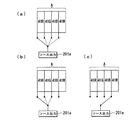
一方、液晶表示装置1において、1つのソースドライバ出力を用いて1つの画素A内の
各サブ画素41R,41G,41B,41Wを時分割駆動するものとしても良い。具体的
には、図6(a)に示すように、透過反射兼用モードでは1つのソース出力201aで透
過表示領域Tの各サブ画素41R,41G,41Bと反射表示領域Rのサブ画素41Wと
を時分割駆動し、図6(b)に示すように、透過モードでは1つのソース出力201aで
透過表示領域Tの各サブ画素41R,41G,41Bを時分割駆動し、図6(c)に示す
ように、反射モードでは1つのソース出力201aで反射表示領域Rのサブ画素41Wの
みを時分割駆動することができる。このような時分割駆動の採用によりソースドライバの
出力数を小さくすることが可能となり、表示に寄与しないサブ画素を選択駆動しないこと
で、表示に寄与するサブ画素へのデータ書き込みのマージンを広げることが可能となる。
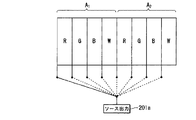
なお、図7に示すように、2画素A1.A2分の各サブ画素41を1つのソース出力20
1aにより時分割駆動することが可能で、場合によっては3画素分の各サブ画素を1つの
ソース出力により時分割駆動することも可能である。
On the other hand, in the liquid
In addition, as shown in FIG. Each sub-pixel 41 for A2 has one
1a can be time-division driven, and in some cases, each sub-pixel for three pixels can be time-division driven by one source output.
[電子機器]
次に、本発明の電子機器について説明する。図8は、本発明に係る電子機器の一例であ
る携帯電話を示す斜視図である。この携帯電話1300は、本発明の液晶表示装置を小サ
イズの表示部1301として備え、複数の操作ボタン1302、受話口1303、及び送
話口1304を備えて構成されている。この電子機器は、前述した本発明の液晶表示装置
を備えているので、透過モードにおいては鮮やかなカラー表示が可能であり、反射モード
においては明るいモノクロ表示が可能である。
[Electronics]
Next, the electronic apparatus of the present invention will be described. FIG. 8 is a perspective view showing a mobile phone as an example of the electronic apparatus according to the present invention. This
なお、上記実施の形態の液晶表示装置は、上記携帯電話に限らず、電子ブック、パーソ
ナルコンピュータ、ディジタルスチルカメラ、液晶テレビ、ビューファインダ型あるいは
モニタ直視型のビデオテープレコーダ、カーナビゲーション装置、ページャ、電子手帳、
電卓、ワードプロセッサ、ワークステーション、テレビ電話、POS端末、タッチパネル
を備えた機器等々の画像表示手段として好適に用いることができ、いずれの電子機器にお
いても、明るく、高コントラストであり、かつ広視野角の透過/反射表示が可能になって
いる。
The liquid crystal display device of the above embodiment is not limited to the mobile phone, but is an electronic book, a personal computer, a digital still camera, a liquid crystal television, a viewfinder type or a monitor direct view type video tape recorder, a car navigation device, a pager, Electronic notebook,
It can be suitably used as an image display means for devices such as calculators, word processors, workstations, videophones, POS terminals, touch panels, etc. In any electronic device, it is bright, has high contrast, and has a wide viewing angle. Transmission / reflection display is possible.
以上、添付図面を参照しながら本発明に係る好適な実施の形態例について説明したが、
本発明は係る例に限定されないことは言うまでもない。また、上述した例において示した
各構成部材の諸形状や組み合わせ等は一例であって、本発明の主旨から逸脱しない範囲に
おいて設計要求等に基づき種々変更可能である。本発明においては、少なくとも透過表示
領域T及び反射表示領域Rがそれぞれ独立に駆動するサブ画素から構成されていればよく
、それ以外の構成については任意に設定することができる。例えば、薄膜トランジスタの
代わりに薄膜ダイオードでスイッチング素子を形成したり、カラーフィルタを下基板(T
FTアレイ基板)側に配設したりすることもできる。また、反射表示領域Rにおいては反
射膜13上に画素電極9を形成するものとしているが、例えば反射膜13を画素電極とし
て用いることも可能である。さらに、前記の実施形態ではTNモードの液晶表示装置につ
いて本発明を適用した例を示したが、STN方式の液晶表示装置、さらにはこれ以外の方
式の液晶表示装置に対して本発明を適用することも可能である。
The preferred embodiment of the present invention has been described above with reference to the accompanying drawings.
It goes without saying that the present invention is not limited to such examples. Further, the shapes and combinations of the constituent members shown in the above-described examples are merely examples, and various modifications can be made based on design requirements and the like without departing from the gist of the present invention. In the present invention, it is sufficient that at least the transmissive display region T and the reflective display region R are composed of sub-pixels that are independently driven, and other configurations can be arbitrarily set. For example, a switching element is formed with a thin film diode instead of a thin film transistor, or a color filter is mounted on a lower substrate (T
It can also be arranged on the FT array substrate side. In the reflective display region R, the
1…液晶表示装置(液晶装置)、1a…液晶パネル、10…TFTアレイ基板(基板)
、20…対向基板(基板)、50…液晶層、41R,41G,41B,41W…サブ画素
、A…画素、T…透過表示領域、R…反射表示領域
DESCRIPTION OF
20 ... counter substrate (substrate), 50 ... liquid crystal layer, 41R, 41G, 41B, 41W ... sub-pixel, A ... pixel, T ... transmissive display area, R ... reflective display area
Claims (10)
各々が異なる色に対応した複数のサブ画素からなる画素を備え、
前記画素の各々には、透過表示を行う透過表示領域と、反射表示を行う反射表示領域と
が配設されてなり、
前記透過表示領域は複数の前記サブ画素から構成される一方、前記反射表示領域は前記
透過表示領域とは別個の前記サブ画素から構成されてなることを特徴とする液晶装置。 A liquid crystal device comprising a liquid crystal panel having a liquid crystal layer sandwiched between a pair of substrates,
Comprising a plurality of sub-pixels each corresponding to a different color;
Each of the pixels is provided with a transmissive display area for performing transmissive display and a reflective display area for performing reflective display.
The transmissive display area is composed of a plurality of the sub-pixels, while the reflective display area is composed of the sub-pixels separate from the transmissive display area.
ー表示又はモノクロ表示が行われることを特徴とする請求項1に記載の液晶装置。 2. The liquid crystal device according to claim 1, wherein full-color display is performed in the transmissive display area, and mono-color display or monochrome display is performed in the reflective display area.
前記ソースドライバは、前記透過表示領域と前記反射表示領域の前記サブ画素を駆動し
て透過表示と反射表示とを行う透過反射兼用モードと、前記透過表示領域に配設されたサ
ブ画素を駆動して透過表示を行う透過モードと、前記反射表示領域に配設されたサブ画素
を駆動して反射表示を行う反射モードとを選択可能であることを特徴とする請求項1又は
2に記載の液晶装置。 A source driver that controls the amount of charge injected into each of the sub-pixels;
The source driver drives the sub-pixels in the transmissive display area and the reflective display area to drive the sub-pixels disposed in the transmissive display area. 3. The liquid crystal according to claim 1, wherein a transmissive mode for performing transmissive display and a reflective mode for performing reflective display by driving a sub-pixel disposed in the reflective display region can be selected. apparatus.
配設され、前記反射モードにおいて前記照明装置が消灯されることを特徴とする請求項3
に記載の液晶装置。 4. An illumination device for irradiating the liquid crystal panel with illumination light is disposed on the opposite side of the liquid crystal panel from the observation side, and the illumination device is turned off in the reflection mode.
The liquid crystal device according to 1.
用モード又は前記透過モードよりも低くされていることを特徴とする請求項3又は4に記
載の液晶装置。 5. The liquid crystal device according to claim 3, wherein, in the reflection mode, a refresh rate for updating display data is set lower than that in the transmission / reflection mode or the transmission mode.
れることを特徴とする請求項3ないし5のいずれか1項に記載の液晶装置。 6. The liquid crystal device according to claim 3, wherein in the reflection mode, the display of the sub-pixels disposed in the transmissive display region is black display.
れることを特徴とする請求項3ないし6のいずれか1項に記載の液晶装置。 7. The liquid crystal device according to claim 3, wherein in the transmissive mode, the display of the sub-pixels disposed in the reflective display region is black display.
ことを特徴とする請求項3ないし7のいずれか1項に記載の液晶装置。 8. The liquid crystal device according to claim 3, wherein each of the sub-pixels in one pixel is time-division driven using one of the source drivers. 9.
ルタ層が配設され、
前記透過表示領域のカラーフィルタ層には、前記各サブ画素毎に異なる色の着色層が配
設される一方、前記反射表示領域のカラーフィルタ層には、前記単一のサブ画素に着色層
又は無色透光層が配設され、
前記反射表示領域の着色層又は無色透光層が前記透過表示領域の着色層よりも前記液晶
層側に突出形成されて、当該反射表示領域の液晶層厚が前記透過表示領域の液晶層厚より
も小さく構成されてなることを特徴とする請求項1ないし8のいずれか1項に記載の液晶
装置。 A color filter layer including a colored layer is disposed on the liquid crystal layer side of at least one of the pair of substrates.
The color filter layer in the transmissive display area is provided with a colored layer having a different color for each of the sub-pixels, while the color filter layer in the reflective display area has a colored layer or A colorless translucent layer is disposed,
A colored layer or a colorless light-transmitting layer in the reflective display region is formed to protrude toward the liquid crystal layer with respect to the colored layer in the transmissive display region, and the liquid crystal layer thickness in the reflective display region is larger than the liquid crystal layer thickness in the transmissive display region. 9. The liquid crystal device according to claim 1, wherein the liquid crystal device is configured to be small.
。
An electronic apparatus comprising the liquid crystal device according to claim 1.
Priority Applications (1)
| Application Number | Priority Date | Filing Date | Title |
|---|---|---|---|
| JP2005309423A JP2007121368A (en) | 2005-10-25 | 2005-10-25 | Liquid crystal device, and electronic device |
Applications Claiming Priority (1)
| Application Number | Priority Date | Filing Date | Title |
|---|---|---|---|
| JP2005309423A JP2007121368A (en) | 2005-10-25 | 2005-10-25 | Liquid crystal device, and electronic device |
Publications (2)
| Publication Number | Publication Date |
|---|---|
| JP2007121368A true JP2007121368A (en) | 2007-05-17 |
| JP2007121368A5 JP2007121368A5 (en) | 2008-02-21 |
Family
ID=38145315
Family Applications (1)
| Application Number | Title | Priority Date | Filing Date |
|---|---|---|---|
| JP2005309423A Pending JP2007121368A (en) | 2005-10-25 | 2005-10-25 | Liquid crystal device, and electronic device |
Country Status (1)
| Country | Link |
|---|---|
| JP (1) | JP2007121368A (en) |
Cited By (8)
| Publication number | Priority date | Publication date | Assignee | Title |
|---|---|---|---|---|
| JP2009008876A (en) * | 2007-06-28 | 2009-01-15 | Epson Imaging Devices Corp | Transflective liquid crystal display panel and electronic equipment |
| JP2009031619A (en) * | 2007-07-30 | 2009-02-12 | Epson Imaging Devices Corp | Transflective liquid crystal display panel |
| WO2011093000A1 (en) * | 2010-01-29 | 2011-08-04 | Semiconductor Energy Laboratory Co., Ltd. | Method for driving liquid crystal display device |
| JP2011170333A (en) * | 2010-01-20 | 2011-09-01 | Semiconductor Energy Lab Co Ltd | Method for driving liquid crystal display device |
| JP2012053455A (en) * | 2010-08-06 | 2012-03-15 | Semiconductor Energy Lab Co Ltd | Liquid crystal display device and its driving method |
| CN103714790A (en) * | 2012-09-28 | 2014-04-09 | 株式会社日本显示器 | Display device and electronic apparatus |
| WO2017110174A1 (en) | 2015-12-22 | 2017-06-29 | カシオ計算機株式会社 | Display device and method for controlling same |
| US11048109B2 (en) | 2015-12-22 | 2021-06-29 | Casio Computer Co., Ltd. | Display module, display device, and method for controlling same |
Citations (5)
| Publication number | Priority date | Publication date | Assignee | Title |
|---|---|---|---|---|
| JPH07159777A (en) * | 1993-12-10 | 1995-06-23 | Casio Comput Co Ltd | Liquid crystal display device |
| JPH11295717A (en) * | 1998-04-13 | 1999-10-29 | Hitachi Ltd | Liquid crystal display device |
| JP2000199897A (en) * | 1999-01-05 | 2000-07-18 | Dainippon Printing Co Ltd | Reflection type liquid crystal display device |
| JP2004177726A (en) * | 2002-11-28 | 2004-06-24 | Sharp Corp | Display device |
| JP2005024680A (en) * | 2003-06-30 | 2005-01-27 | Toppoly Optoelectronics Corp | Transmission/reflection liquid crystal display |
-
2005
- 2005-10-25 JP JP2005309423A patent/JP2007121368A/en active Pending
Patent Citations (5)
| Publication number | Priority date | Publication date | Assignee | Title |
|---|---|---|---|---|
| JPH07159777A (en) * | 1993-12-10 | 1995-06-23 | Casio Comput Co Ltd | Liquid crystal display device |
| JPH11295717A (en) * | 1998-04-13 | 1999-10-29 | Hitachi Ltd | Liquid crystal display device |
| JP2000199897A (en) * | 1999-01-05 | 2000-07-18 | Dainippon Printing Co Ltd | Reflection type liquid crystal display device |
| JP2004177726A (en) * | 2002-11-28 | 2004-06-24 | Sharp Corp | Display device |
| JP2005024680A (en) * | 2003-06-30 | 2005-01-27 | Toppoly Optoelectronics Corp | Transmission/reflection liquid crystal display |
Cited By (20)
| Publication number | Priority date | Publication date | Assignee | Title |
|---|---|---|---|---|
| JP2009008876A (en) * | 2007-06-28 | 2009-01-15 | Epson Imaging Devices Corp | Transflective liquid crystal display panel and electronic equipment |
| JP2009031619A (en) * | 2007-07-30 | 2009-02-12 | Epson Imaging Devices Corp | Transflective liquid crystal display panel |
| TWI603312B (en) * | 2010-01-20 | 2017-10-21 | 半導體能源研究所股份有限公司 | Method for driving liquid crystal display device |
| TWI562121B (en) * | 2010-01-20 | 2016-12-11 | Semiconductor Energy Lab Co Ltd | Method for driving liquid crystal display device |
| JP2011170333A (en) * | 2010-01-20 | 2011-09-01 | Semiconductor Energy Lab Co Ltd | Method for driving liquid crystal display device |
| JP2011175251A (en) * | 2010-01-29 | 2011-09-08 | Semiconductor Energy Lab Co Ltd | Method for driving liquid crystal display device |
| WO2011093000A1 (en) * | 2010-01-29 | 2011-08-04 | Semiconductor Energy Laboratory Co., Ltd. | Method for driving liquid crystal display device |
| TWI651705B (en) * | 2010-01-29 | 2019-02-21 | 日商半導體能源研究所股份有限公司 | Driving method of liquid crystal display device |
| US20110187758A1 (en) * | 2010-01-29 | 2011-08-04 | Semiconductor Energy Laboratory Co., Ltd. | Method for driving liquid crystal display device |
| US9076401B2 (en) | 2010-01-29 | 2015-07-07 | Semiconductor Energy Laboratory Co., Ltd. | Method for driving liquid crystal display device |
| US9507220B2 (en) | 2010-08-06 | 2016-11-29 | Semiconductor Energy Laboratory Co., Ltd. | Liquid crystal display device and driving method thereof |
| JP2012053455A (en) * | 2010-08-06 | 2012-03-15 | Semiconductor Energy Lab Co Ltd | Liquid crystal display device and its driving method |
| US9208744B2 (en) | 2012-09-28 | 2015-12-08 | Japan Display Inc. | Display device and electronic apparatus |
| CN103714790B (en) * | 2012-09-28 | 2016-06-01 | 株式会社日本显示器 | Display unit and electronics |
| JP2014071372A (en) * | 2012-09-28 | 2014-04-21 | Japan Display Inc | Display device and electronic equipment |
| CN103714790A (en) * | 2012-09-28 | 2014-04-09 | 株式会社日本显示器 | Display device and electronic apparatus |
| WO2017110174A1 (en) | 2015-12-22 | 2017-06-29 | カシオ計算機株式会社 | Display device and method for controlling same |
| US11048109B2 (en) | 2015-12-22 | 2021-06-29 | Casio Computer Co., Ltd. | Display module, display device, and method for controlling same |
| US11079835B2 (en) | 2015-12-22 | 2021-08-03 | Casio Computer Co., Ltd. | Display device and method for controlling same |
| US11194383B2 (en) | 2015-12-22 | 2021-12-07 | Casio Computer Co., Ltd. | Display device and method for controlling same |
Similar Documents
| Publication | Publication Date | Title |
|---|---|---|
| JP4539760B2 (en) | Electronics | |
| JP4607158B2 (en) | Liquid crystal display device and electronic device | |
| JP5623982B2 (en) | Transflective display device and electronic device | |
| JP2006071987A (en) | Liquid crystal display device, and electronic apparatus | |
| JP2007121368A (en) | Liquid crystal device, and electronic device | |
| US9093043B2 (en) | Display device and electronic apparatus | |
| JP2007334224A (en) | Liquid crystal display | |
| JP2007058007A (en) | Liquid crystal device and electronic apparatus | |
| JP2007279719A (en) | Image display system | |
| US7995169B2 (en) | Liquid crystal display device and electronic apparatus | |
| US9188824B2 (en) | Display device | |
| JP5175133B2 (en) | Liquid crystal device and electronic device | |
| JP4428330B2 (en) | Electro-optical device and electronic apparatus | |
| JP2005173565A (en) | Liquid crystal display device | |
| JP2009075421A (en) | Liquid crystal device and electronic equipment | |
| JP4305485B2 (en) | Liquid crystal device, driving method of liquid crystal device, projector and electronic apparatus | |
| JP5177984B2 (en) | Liquid crystal device and electronic device | |
| US8233121B2 (en) | Display panel and color filter substrate | |
| KR20080066565A (en) | Display device | |
| JP2007086506A (en) | Electrooptical device and electronic equipment | |
| JP2008009042A (en) | Liquid crystal display device and electronic equipment | |
| US20190011774A1 (en) | Display device | |
| JP2008180929A (en) | Liquid crystal display device and driving method of the same | |
| JP6255973B2 (en) | Electro-optical device and electronic apparatus | |
| JP2008083484A (en) | Liquid crystal device, its driving method, and electronic equipment |
Legal Events
| Date | Code | Title | Description |
|---|---|---|---|
| RD04 | Notification of resignation of power of attorney |
Free format text: JAPANESE INTERMEDIATE CODE: A7424 Effective date: 20070404 |
|
| A521 | Written amendment |
Free format text: JAPANESE INTERMEDIATE CODE: A523 Effective date: 20080107 |
|
| A621 | Written request for application examination |
Free format text: JAPANESE INTERMEDIATE CODE: A621 Effective date: 20080107 |
|
| A711 | Notification of change in applicant |
Free format text: JAPANESE INTERMEDIATE CODE: A711 Effective date: 20100526 |
|
| RD02 | Notification of acceptance of power of attorney |
Free format text: JAPANESE INTERMEDIATE CODE: A7422 Effective date: 20100526 |
|
| A977 | Report on retrieval |
Free format text: JAPANESE INTERMEDIATE CODE: A971007 Effective date: 20110125 |
|
| A131 | Notification of reasons for refusal |
Free format text: JAPANESE INTERMEDIATE CODE: A131 Effective date: 20110215 |
|
| A02 | Decision of refusal |
Free format text: JAPANESE INTERMEDIATE CODE: A02 Effective date: 20110628 |