JP2007080896A - 半導体素子 - Google Patents
半導体素子 Download PDFInfo
- Publication number
- JP2007080896A JP2007080896A JP2005263264A JP2005263264A JP2007080896A JP 2007080896 A JP2007080896 A JP 2007080896A JP 2005263264 A JP2005263264 A JP 2005263264A JP 2005263264 A JP2005263264 A JP 2005263264A JP 2007080896 A JP2007080896 A JP 2007080896A
- Authority
- JP
- Japan
- Prior art keywords
- layer
- semiconductor
- substrate
- nitride
- composition ratio
- Prior art date
- Legal status (The legal status is an assumption and is not a legal conclusion. Google has not performed a legal analysis and makes no representation as to the accuracy of the status listed.)
- Pending
Links
Images


Classifications
-
- H—ELECTRICITY
- H01—ELECTRIC ELEMENTS
- H01S—DEVICES USING THE PROCESS OF LIGHT AMPLIFICATION BY STIMULATED EMISSION OF RADIATION [LASER] TO AMPLIFY OR GENERATE LIGHT; DEVICES USING STIMULATED EMISSION OF ELECTROMAGNETIC RADIATION IN WAVE RANGES OTHER THAN OPTICAL
- H01S5/00—Semiconductor lasers
- H01S5/30—Structure or shape of the active region; Materials used for the active region
- H01S5/34—Structure or shape of the active region; Materials used for the active region comprising quantum well or superlattice structures, e.g. single quantum well [SQW] lasers, multiple quantum well [MQW] lasers or graded index separate confinement heterostructure [GRINSCH] lasers
- H01S5/343—Structure or shape of the active region; Materials used for the active region comprising quantum well or superlattice structures, e.g. single quantum well [SQW] lasers, multiple quantum well [MQW] lasers or graded index separate confinement heterostructure [GRINSCH] lasers in AIIIBV compounds, e.g. AlGaAs-laser, InP-based laser
- H01S5/34333—Structure or shape of the active region; Materials used for the active region comprising quantum well or superlattice structures, e.g. single quantum well [SQW] lasers, multiple quantum well [MQW] lasers or graded index separate confinement heterostructure [GRINSCH] lasers in AIIIBV compounds, e.g. AlGaAs-laser, InP-based laser with a well layer based on Ga(In)N or Ga(In)P, e.g. blue laser
-
- B—PERFORMING OPERATIONS; TRANSPORTING
- B82—NANOTECHNOLOGY
- B82Y—SPECIFIC USES OR APPLICATIONS OF NANOSTRUCTURES; MEASUREMENT OR ANALYSIS OF NANOSTRUCTURES; MANUFACTURE OR TREATMENT OF NANOSTRUCTURES
- B82Y20/00—Nanooptics, e.g. quantum optics or photonic crystals
-
- H—ELECTRICITY
- H01—ELECTRIC ELEMENTS
- H01L—SEMICONDUCTOR DEVICES NOT COVERED BY CLASS H10
- H01L33/00—Semiconductor devices with at least one potential-jump barrier or surface barrier specially adapted for light emission; Processes or apparatus specially adapted for the manufacture or treatment thereof or of parts thereof; Details thereof
- H01L33/02—Semiconductor devices with at least one potential-jump barrier or surface barrier specially adapted for light emission; Processes or apparatus specially adapted for the manufacture or treatment thereof or of parts thereof; Details thereof characterised by the semiconductor bodies
- H01L33/26—Materials of the light emitting region
- H01L33/30—Materials of the light emitting region containing only elements of group III and group V of the periodic system
- H01L33/32—Materials of the light emitting region containing only elements of group III and group V of the periodic system containing nitrogen
-
- H—ELECTRICITY
- H01—ELECTRIC ELEMENTS
- H01L—SEMICONDUCTOR DEVICES NOT COVERED BY CLASS H10
- H01L33/00—Semiconductor devices with at least one potential-jump barrier or surface barrier specially adapted for light emission; Processes or apparatus specially adapted for the manufacture or treatment thereof or of parts thereof; Details thereof
- H01L33/005—Processes
- H01L33/0062—Processes for devices with an active region comprising only III-V compounds
- H01L33/0075—Processes for devices with an active region comprising only III-V compounds comprising nitride compounds
-
- H—ELECTRICITY
- H01—ELECTRIC ELEMENTS
- H01L—SEMICONDUCTOR DEVICES NOT COVERED BY CLASS H10
- H01L33/00—Semiconductor devices with at least one potential-jump barrier or surface barrier specially adapted for light emission; Processes or apparatus specially adapted for the manufacture or treatment thereof or of parts thereof; Details thereof
- H01L33/02—Semiconductor devices with at least one potential-jump barrier or surface barrier specially adapted for light emission; Processes or apparatus specially adapted for the manufacture or treatment thereof or of parts thereof; Details thereof characterised by the semiconductor bodies
- H01L33/12—Semiconductor devices with at least one potential-jump barrier or surface barrier specially adapted for light emission; Processes or apparatus specially adapted for the manufacture or treatment thereof or of parts thereof; Details thereof characterised by the semiconductor bodies with a stress relaxation structure, e.g. buffer layer
-
- H—ELECTRICITY
- H01—ELECTRIC ELEMENTS
- H01S—DEVICES USING THE PROCESS OF LIGHT AMPLIFICATION BY STIMULATED EMISSION OF RADIATION [LASER] TO AMPLIFY OR GENERATE LIGHT; DEVICES USING STIMULATED EMISSION OF ELECTROMAGNETIC RADIATION IN WAVE RANGES OTHER THAN OPTICAL
- H01S2301/00—Functional characteristics
- H01S2301/17—Semiconductor lasers comprising special layers
- H01S2301/173—The laser chip comprising special buffer layers, e.g. dislocation prevention or reduction
-
- H—ELECTRICITY
- H01—ELECTRIC ELEMENTS
- H01S—DEVICES USING THE PROCESS OF LIGHT AMPLIFICATION BY STIMULATED EMISSION OF RADIATION [LASER] TO AMPLIFY OR GENERATE LIGHT; DEVICES USING STIMULATED EMISSION OF ELECTROMAGNETIC RADIATION IN WAVE RANGES OTHER THAN OPTICAL
- H01S2304/00—Special growth methods for semiconductor lasers
- H01S2304/04—MOCVD or MOVPE
-
- H—ELECTRICITY
- H01—ELECTRIC ELEMENTS
- H01S—DEVICES USING THE PROCESS OF LIGHT AMPLIFICATION BY STIMULATED EMISSION OF RADIATION [LASER] TO AMPLIFY OR GENERATE LIGHT; DEVICES USING STIMULATED EMISSION OF ELECTROMAGNETIC RADIATION IN WAVE RANGES OTHER THAN OPTICAL
- H01S2304/00—Special growth methods for semiconductor lasers
- H01S2304/12—Pendeo epitaxial lateral overgrowth [ELOG], e.g. for growing GaN based blue laser diodes
-
- H—ELECTRICITY
- H01—ELECTRIC ELEMENTS
- H01S—DEVICES USING THE PROCESS OF LIGHT AMPLIFICATION BY STIMULATED EMISSION OF RADIATION [LASER] TO AMPLIFY OR GENERATE LIGHT; DEVICES USING STIMULATED EMISSION OF ELECTROMAGNETIC RADIATION IN WAVE RANGES OTHER THAN OPTICAL
- H01S5/00—Semiconductor lasers
- H01S5/02—Structural details or components not essential to laser action
- H01S5/0206—Substrates, e.g. growth, shape, material, removal or bonding
- H01S5/0217—Removal of the substrate
-
- H—ELECTRICITY
- H01—ELECTRIC ELEMENTS
- H01S—DEVICES USING THE PROCESS OF LIGHT AMPLIFICATION BY STIMULATED EMISSION OF RADIATION [LASER] TO AMPLIFY OR GENERATE LIGHT; DEVICES USING STIMULATED EMISSION OF ELECTROMAGNETIC RADIATION IN WAVE RANGES OTHER THAN OPTICAL
- H01S5/00—Semiconductor lasers
- H01S5/20—Structure or shape of the semiconductor body to guide the optical wave ; Confining structures perpendicular to the optical axis, e.g. index or gain guiding, stripe geometry, broad area lasers, gain tailoring, transverse or lateral reflectors, special cladding structures, MQW barrier reflection layers
- H01S5/2004—Confining in the direction perpendicular to the layer structure
- H01S5/2009—Confining in the direction perpendicular to the layer structure by using electron barrier layers
-
- H—ELECTRICITY
- H01—ELECTRIC ELEMENTS
- H01S—DEVICES USING THE PROCESS OF LIGHT AMPLIFICATION BY STIMULATED EMISSION OF RADIATION [LASER] TO AMPLIFY OR GENERATE LIGHT; DEVICES USING STIMULATED EMISSION OF ELECTROMAGNETIC RADIATION IN WAVE RANGES OTHER THAN OPTICAL
- H01S5/00—Semiconductor lasers
- H01S5/20—Structure or shape of the semiconductor body to guide the optical wave ; Confining structures perpendicular to the optical axis, e.g. index or gain guiding, stripe geometry, broad area lasers, gain tailoring, transverse or lateral reflectors, special cladding structures, MQW barrier reflection layers
- H01S5/22—Structure or shape of the semiconductor body to guide the optical wave ; Confining structures perpendicular to the optical axis, e.g. index or gain guiding, stripe geometry, broad area lasers, gain tailoring, transverse or lateral reflectors, special cladding structures, MQW barrier reflection layers having a ridge or stripe structure
- H01S5/2205—Structure or shape of the semiconductor body to guide the optical wave ; Confining structures perpendicular to the optical axis, e.g. index or gain guiding, stripe geometry, broad area lasers, gain tailoring, transverse or lateral reflectors, special cladding structures, MQW barrier reflection layers having a ridge or stripe structure comprising special burying or current confinement layers
- H01S5/2214—Structure or shape of the semiconductor body to guide the optical wave ; Confining structures perpendicular to the optical axis, e.g. index or gain guiding, stripe geometry, broad area lasers, gain tailoring, transverse or lateral reflectors, special cladding structures, MQW barrier reflection layers having a ridge or stripe structure comprising special burying or current confinement layers based on oxides or nitrides
-
- H—ELECTRICITY
- H01—ELECTRIC ELEMENTS
- H01S—DEVICES USING THE PROCESS OF LIGHT AMPLIFICATION BY STIMULATED EMISSION OF RADIATION [LASER] TO AMPLIFY OR GENERATE LIGHT; DEVICES USING STIMULATED EMISSION OF ELECTROMAGNETIC RADIATION IN WAVE RANGES OTHER THAN OPTICAL
- H01S5/00—Semiconductor lasers
- H01S5/20—Structure or shape of the semiconductor body to guide the optical wave ; Confining structures perpendicular to the optical axis, e.g. index or gain guiding, stripe geometry, broad area lasers, gain tailoring, transverse or lateral reflectors, special cladding structures, MQW barrier reflection layers
- H01S5/22—Structure or shape of the semiconductor body to guide the optical wave ; Confining structures perpendicular to the optical axis, e.g. index or gain guiding, stripe geometry, broad area lasers, gain tailoring, transverse or lateral reflectors, special cladding structures, MQW barrier reflection layers having a ridge or stripe structure
- H01S5/223—Buried stripe structure
- H01S5/2231—Buried stripe structure with inner confining structure only between the active layer and the upper electrode
Abstract
【解決手段】この半導体素子(窒化物系半導体レーザ素子)は、2種類の3族元素であるAlおよびGaと窒素とからなるAlGaN基板1と活性層5との間に、AlGaN基板1と同一の構成元素からなるとともに、Al0.07Ga0.93NからなるAlGaN基板1のAl組成比(7%)より高いAl組成比(15%)を有するAl0.15Ga0.85Nからなる高Al組成層2が形成されている。
【選択図】図1
Description
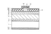
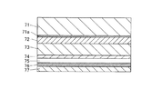
図1は、本発明の第1実施形態による窒化物系半導体レーザ素子(半導体素子)の構造を示した断面図である。図2は、図1に示した第1実施形態による窒化物系半導体レーザ素子の活性層の構造を示した断面図である。まず、図1および図2を参照して、第1実施形態による窒化物系半導体レーザ素子の構造について説明する。
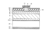
図7は、本発明の第2実施形態による窒化物系半導体レーザ素子の構造を示した断面図である。図7を参照して、この第2実施形態では、上記第1実施形態と異なり、高Al組成層21aが、AlGaN基板21の表面が変質された変質層からなる場合の構造について説明する。なお、第2実施形態のAlGaN基板21および高Al組成層21a以外の構造は、上記第1実施形態と同じであるため、高Al組成層21a以外の構造については説明を省略する。なお、AlGaN基板21は、本発明の「半導体基板」の一例である。
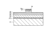
図8は、本発明の第3実施形態による窒化物系半導体レーザ素子(半導体素子)の構造を示した断面図である。図8を参照して、この第3実施形態では、上記第1および第2実施形態とは異なり、InGaN基板31上に変質層からなる高Ga組成層31aを形成した場合について説明する。
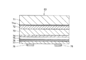
図12は、本発明の第4実施形態による窒化物系半導体発光ダイオード(LED)素子(半導体素子)の構造を示した断面図である。図13は、図12に示した第4実施形態による窒化物系半導体LED素子内部の歪の補償構造を説明するための断面図である。図12および図13を参照して、この第4実施形態では、上記第1〜第3実施形態とは異なり、AlGaNからなるn型クラッド層58と活性層56との間に歪補償層57を形成する場合について説明する。
図22は、本発明の第5実施形態による窒化物系半導体LED素子の構造を示した断面図である。図22を参照して、この第5実施形態では、上記第1〜第4実施形態と異なり、n型クラッド層68と活性層56との間に形成された歪補償層68aがn型クラッド層68の変質層からなる場合の構造について説明する。なお、この第5実施形態では、n型クラッド層68および歪補償層68a以外の構造については、上記第4実施形態と同様であるため、n型クラッド層68および歪補償層68a以外の構造については説明を省略する。
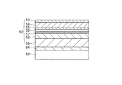
図23は、本発明の第6実施形態による窒化物系半導体LED素子(半導体素子)の構造を示した断面図である。図23を参照して、この第6実施形態では、上記第1〜第5実施形態とは異なり、In0.1Ga0.9Nからなるn型クラッド層77と活性層75との間に歪補償層76を形成する場合について説明する。
2、21a 高Al組成層(窒化物系半導体層)
3 バッファ層
43、64、80 低温バッファ層
4、32、58、68、77 n型クラッド層
5、34、56、75 活性層
8、54、73 p型クラッド層
9 p側コンタクト層
37、53 p型コンタクト層
10、39 電流ブロック層
15、38 リッジ部
31 InGaN基板(半導体基板)
31a 高Ga組成層(窒化物系半導体層)
40、52、72 p側電極
41、62、78 n側電極
57、68a、76 歪補償層(窒化物系半導体層)
59 n型コンタクト層
Claims (13)
- 少なくとも2種類の3族元素と窒素とからなる半導体基板と、
前記半導体基板上に形成される活性層と、
前記半導体基板と前記活性層との間の前記半導体基板の上面に形成されるとともに、前記半導体基板の構成元素と同一の構成元素からなり、かつ、前記構成元素の少なくとも2種類の3族元素の内、最も軽い元素の組成比が前記半導体基板の対応する元素の組成比よりも高い窒化物系半導体層とを備えた、半導体素子。 - 前記半導体基板の構成元素と同一の構成元素からなるクラッド層をさらに備える、請求項1に記載の半導体素子。
- 前記半導体基板および前記窒化物系半導体層は、AlGaN層であり、
前記窒化物系半導体層のAl組成比は、前記半導体基板のAl組成比より高い、請求項1または2に記載の半導体素子。 - 前記半導体基板および前記窒化物系半導体層は、InGaN層であり、
前記窒化物系半導体層のGa組成比は、前記半導体基板のGa組成比より高い、請求項1または2に記載の半導体素子。 - 前記窒化物系半導体層は、前記半導体基板の上面上に接触するように形成されている、請求項1〜4のいずれか1項に記載の半導体素子。
- 前記窒化物系半導体層は、前記半導体基板の表面が変質された変質層からなる、請求項1〜4のいずれか1項に記載の半導体素子。
- 少なくとも2種類の3族元素と窒素とからなる半導体層と、
活性層と、
前記活性層の前記半導体層とは反対側の面側に接着層により接着された基板と、
前記半導体層と前記活性層との間の前記半導体層の表面に形成されるとともに、前記半導体層の構成元素と同一の構成元素からなり、かつ、前記構成元素の少なくとも2種類の3族元素の内、最も軽い元素の組成比が前記半導体層の対応する元素の組成比よりも高い窒化物系半導体層とを備えた、半導体素子。 - 前記活性層には、前記活性層を構成する層の主表面に沿った方向の圧縮歪が印加されている、請求項7に記載の半導体素子。
- 前記半導体層は、前記活性層よりも大きい格子定数を有する、請求項7または8に記載の半導体素子。
- 前記半導体層および前記窒化物系半導体層は、AlGaN層であり、
前記窒化物系半導体層のAl組成比は、前記半導体層のAl組成比より高い、請求項7〜9のいずれか1項に記載の半導体素子。 - 前記半導体層および前記窒化物系半導体層は、InGaN層であり、
前記窒化物系半導体層のGa組成比は、前記半導体層のGa組成比より高い、請求項7〜9のいずれか1項に記載の半導体素子。 - 前記窒化物系半導体層は、前記半導体層の前記活性層側の表面上に、前記半導体層に接触するように形成されている、請求項7〜11に記載の半導体素子。
- 前記窒化物系半導体層は、前記半導体層の前記活性層側の表面が変質された変質層からなる、請求項7〜11に記載の半導体素子。
Priority Applications (3)
| Application Number | Priority Date | Filing Date | Title |
|---|---|---|---|
| JP2005263264A JP2007080896A (ja) | 2005-09-12 | 2005-09-12 | 半導体素子 |
| US11/518,235 US7518204B2 (en) | 2005-09-12 | 2006-09-11 | Semiconductor device |
| US12/402,196 US8334577B2 (en) | 2005-09-12 | 2009-03-11 | Semiconductor device |
Applications Claiming Priority (1)
| Application Number | Priority Date | Filing Date | Title |
|---|---|---|---|
| JP2005263264A JP2007080896A (ja) | 2005-09-12 | 2005-09-12 | 半導体素子 |
Publications (2)
| Publication Number | Publication Date |
|---|---|
| JP2007080896A true JP2007080896A (ja) | 2007-03-29 |
| JP2007080896A5 JP2007080896A5 (ja) | 2007-09-20 |
Family
ID=37854237
Family Applications (1)
| Application Number | Title | Priority Date | Filing Date |
|---|---|---|---|
| JP2005263264A Pending JP2007080896A (ja) | 2005-09-12 | 2005-09-12 | 半導体素子 |
Country Status (2)
| Country | Link |
|---|---|
| US (2) | US7518204B2 (ja) |
| JP (1) | JP2007080896A (ja) |
Cited By (11)
| Publication number | Priority date | Publication date | Assignee | Title |
|---|---|---|---|---|
| JP2008153531A (ja) * | 2006-12-19 | 2008-07-03 | Sumitomo Electric Ind Ltd | 半導体発光素子 |
| JP2008300700A (ja) * | 2007-05-31 | 2008-12-11 | Sanyo Electric Co Ltd | 窒化物系半導体レーザおよびその製造方法 |
| JP2009238803A (ja) * | 2008-03-26 | 2009-10-15 | Furukawa Electric Co Ltd:The | GaN系半導体基板、その製造方法および半導体素子 |
| JP2009277724A (ja) * | 2008-05-12 | 2009-11-26 | Sumitomo Electric Ind Ltd | 窒化物半導体レーザ |
| JP2010056234A (ja) * | 2008-08-27 | 2010-03-11 | Sumitomo Electric Ind Ltd | 窒化物系半導体発光素子を作製する方法、及びエピタキシャルウエハを作製する方法 |
| JP2010093128A (ja) * | 2008-10-09 | 2010-04-22 | Nec Corp | 半導体発光素子 |
| JP2010531058A (ja) * | 2007-06-22 | 2010-09-16 | エルジー イノテック カンパニー リミテッド | 半導体発光素子及びその製造方法 |
| JP2011513954A (ja) * | 2008-02-29 | 2011-04-28 | オスラム オプト セミコンダクターズ ゲゼルシャフト ミット ベシュレンクテル ハフツング | オプトエレクトロニクス素子およびオプトエレクトロニクス素子の製造方法 |
| JP2012074740A (ja) * | 2011-12-28 | 2012-04-12 | Sumitomo Electric Ind Ltd | 半導体発光素子 |
| JP2014508416A (ja) * | 2011-02-28 | 2014-04-03 | コーニング インコーポレイテッド | インジウム含有クラッド層を有する半導体レーザ |
| JP2019091801A (ja) * | 2017-11-14 | 2019-06-13 | シャープ株式会社 | 窒化物半導体レーザ素子 |
Families Citing this family (64)
| Publication number | Priority date | Publication date | Assignee | Title |
|---|---|---|---|---|
| US7707603B2 (en) * | 2005-01-28 | 2010-04-27 | Microsoft Corporation | Digital media transfer based on user behavior |
| JP2007080896A (ja) * | 2005-09-12 | 2007-03-29 | Sanyo Electric Co Ltd | 半導体素子 |
| KR100661602B1 (ko) * | 2005-12-09 | 2006-12-26 | 삼성전기주식회사 | 수직 구조 질화갈륨계 led 소자의 제조방법 |
| US20090238227A1 (en) * | 2008-03-05 | 2009-09-24 | Rohm Co., Ltd. | Semiconductor light emitting device |
| US20090301388A1 (en) * | 2008-06-05 | 2009-12-10 | Soraa Inc. | Capsule for high pressure processing and method of use for supercritical fluids |
| US8871024B2 (en) * | 2008-06-05 | 2014-10-28 | Soraa, Inc. | High pressure apparatus and method for nitride crystal growth |
| US8097081B2 (en) | 2008-06-05 | 2012-01-17 | Soraa, Inc. | High pressure apparatus and method for nitride crystal growth |
| US9157167B1 (en) | 2008-06-05 | 2015-10-13 | Soraa, Inc. | High pressure apparatus and method for nitride crystal growth |
| US8303710B2 (en) * | 2008-06-18 | 2012-11-06 | Soraa, Inc. | High pressure apparatus and method for nitride crystal growth |
| US20100006873A1 (en) * | 2008-06-25 | 2010-01-14 | Soraa, Inc. | HIGHLY POLARIZED WHITE LIGHT SOURCE BY COMBINING BLUE LED ON SEMIPOLAR OR NONPOLAR GaN WITH YELLOW LED ON SEMIPOLAR OR NONPOLAR GaN |
| US20090320745A1 (en) * | 2008-06-25 | 2009-12-31 | Soraa, Inc. | Heater device and method for high pressure processing of crystalline materials |
| WO2010005914A1 (en) * | 2008-07-07 | 2010-01-14 | Soraa, Inc. | High quality large area bulk non-polar or semipolar gallium based substrates and methods |
| US9404197B2 (en) | 2008-07-07 | 2016-08-02 | Soraa, Inc. | Large area, low-defect gallium-containing nitride crystals, method of making, and method of use |
| US8124996B2 (en) | 2008-08-04 | 2012-02-28 | Soraa, Inc. | White light devices using non-polar or semipolar gallium containing materials and phosphors |
| US8284810B1 (en) | 2008-08-04 | 2012-10-09 | Soraa, Inc. | Solid state laser device using a selected crystal orientation in non-polar or semi-polar GaN containing materials and methods |
| US8021481B2 (en) | 2008-08-07 | 2011-09-20 | Soraa, Inc. | Process and apparatus for large-scale manufacturing of bulk monocrystalline gallium-containing nitride |
| US10036099B2 (en) | 2008-08-07 | 2018-07-31 | Slt Technologies, Inc. | Process for large-scale ammonothermal manufacturing of gallium nitride boules |
| US20100031873A1 (en) * | 2008-08-07 | 2010-02-11 | Soraa, Inc. | Basket process and apparatus for crystalline gallium-containing nitride |
| US8430958B2 (en) | 2008-08-07 | 2013-04-30 | Soraa, Inc. | Apparatus and method for seed crystal utilization in large-scale manufacturing of gallium nitride |
| US8323405B2 (en) | 2008-08-07 | 2012-12-04 | Soraa, Inc. | Process and apparatus for growing a crystalline gallium-containing nitride using an azide mineralizer |
| US8979999B2 (en) | 2008-08-07 | 2015-03-17 | Soraa, Inc. | Process for large-scale ammonothermal manufacturing of gallium nitride boules |
| US7976630B2 (en) | 2008-09-11 | 2011-07-12 | Soraa, Inc. | Large-area seed for ammonothermal growth of bulk gallium nitride and method of manufacture |
| US8354679B1 (en) | 2008-10-02 | 2013-01-15 | Soraa, Inc. | Microcavity light emitting diode method of manufacture |
| US8455894B1 (en) | 2008-10-17 | 2013-06-04 | Soraa, Inc. | Photonic-crystal light emitting diode and method of manufacture |
| USRE47114E1 (en) | 2008-12-12 | 2018-11-06 | Slt Technologies, Inc. | Polycrystalline group III metal nitride with getter and method of making |
| US20100147210A1 (en) * | 2008-12-12 | 2010-06-17 | Soraa, Inc. | high pressure apparatus and method for nitride crystal growth |
| US8987156B2 (en) | 2008-12-12 | 2015-03-24 | Soraa, Inc. | Polycrystalline group III metal nitride with getter and method of making |
| US8461071B2 (en) * | 2008-12-12 | 2013-06-11 | Soraa, Inc. | Polycrystalline group III metal nitride with getter and method of making |
| US8878230B2 (en) * | 2010-03-11 | 2014-11-04 | Soraa, Inc. | Semi-insulating group III metal nitride and method of manufacture |
| US9543392B1 (en) | 2008-12-12 | 2017-01-10 | Soraa, Inc. | Transparent group III metal nitride and method of manufacture |
| US9589792B2 (en) | 2012-11-26 | 2017-03-07 | Soraa, Inc. | High quality group-III metal nitride crystals, methods of making, and methods of use |
| US20110100291A1 (en) * | 2009-01-29 | 2011-05-05 | Soraa, Inc. | Plant and method for large-scale ammonothermal manufacturing of gallium nitride boules |
| US8299473B1 (en) | 2009-04-07 | 2012-10-30 | Soraa, Inc. | Polarized white light devices using non-polar or semipolar gallium containing materials and transparent phosphors |
| US8306081B1 (en) * | 2009-05-27 | 2012-11-06 | Soraa, Inc. | High indium containing InGaN substrates for long wavelength optical devices |
| US8509275B1 (en) | 2009-05-29 | 2013-08-13 | Soraa, Inc. | Gallium nitride based laser dazzling device and method |
| US9800017B1 (en) | 2009-05-29 | 2017-10-24 | Soraa Laser Diode, Inc. | Laser device and method for a vehicle |
| US9250044B1 (en) | 2009-05-29 | 2016-02-02 | Soraa Laser Diode, Inc. | Gallium and nitrogen containing laser diode dazzling devices and methods of use |
| DE102009040438A1 (de) * | 2009-07-24 | 2011-01-27 | Osram Opto Semiconductors Gmbh | Optoelektronischer Halbleiterkörper mit einer Quantentopfstruktur |
| US8435347B2 (en) | 2009-09-29 | 2013-05-07 | Soraa, Inc. | High pressure apparatus with stackable rings |
| US9175418B2 (en) | 2009-10-09 | 2015-11-03 | Soraa, Inc. | Method for synthesis of high quality large area bulk gallium based crystals |
| KR101007087B1 (ko) * | 2009-10-26 | 2011-01-10 | 엘지이노텍 주식회사 | 발광소자 및 그 제조방법 |
| US9564320B2 (en) | 2010-06-18 | 2017-02-07 | Soraa, Inc. | Large area nitride crystal and method for making it |
| KR20130108058A (ko) * | 2010-09-16 | 2013-10-02 | 스미토모덴키고교가부시키가이샤 | 반도체 장치의 제조 방법 |
| US8729559B2 (en) | 2010-10-13 | 2014-05-20 | Soraa, Inc. | Method of making bulk InGaN substrates and devices thereon |
| JP5002703B2 (ja) * | 2010-12-08 | 2012-08-15 | 株式会社東芝 | 半導体発光素子 |
| US8786053B2 (en) | 2011-01-24 | 2014-07-22 | Soraa, Inc. | Gallium-nitride-on-handle substrate materials and devices and method of manufacture |
| US8492185B1 (en) | 2011-07-14 | 2013-07-23 | Soraa, Inc. | Large area nonpolar or semipolar gallium and nitrogen containing substrate and resulting devices |
| US9694158B2 (en) | 2011-10-21 | 2017-07-04 | Ahmad Mohamad Slim | Torque for incrementally advancing a catheter during right heart catheterization |
| US10029955B1 (en) | 2011-10-24 | 2018-07-24 | Slt Technologies, Inc. | Capsule for high pressure, high temperature processing of materials and methods of use |
| US8482104B2 (en) | 2012-01-09 | 2013-07-09 | Soraa, Inc. | Method for growth of indium-containing nitride films |
| JP5319810B2 (ja) * | 2012-03-08 | 2013-10-16 | 株式会社東芝 | 窒化物半導体層の製造方法 |
| US10145026B2 (en) | 2012-06-04 | 2018-12-04 | Slt Technologies, Inc. | Process for large-scale ammonothermal manufacturing of semipolar gallium nitride boules |
| US9275912B1 (en) | 2012-08-30 | 2016-03-01 | Soraa, Inc. | Method for quantification of extended defects in gallium-containing nitride crystals |
| US9299555B1 (en) | 2012-09-28 | 2016-03-29 | Soraa, Inc. | Ultrapure mineralizers and methods for nitride crystal growth |
| US9650723B1 (en) | 2013-04-11 | 2017-05-16 | Soraa, Inc. | Large area seed crystal for ammonothermal crystal growth and method of making |
| CN104134729B (zh) * | 2013-05-03 | 2017-04-26 | 展晶科技(深圳)有限公司 | 发光芯片及其制造方法 |
| US10174438B2 (en) | 2017-03-30 | 2019-01-08 | Slt Technologies, Inc. | Apparatus for high pressure reaction |
| US11421843B2 (en) | 2018-12-21 | 2022-08-23 | Kyocera Sld Laser, Inc. | Fiber-delivered laser-induced dynamic light system |
| US11239637B2 (en) | 2018-12-21 | 2022-02-01 | Kyocera Sld Laser, Inc. | Fiber delivered laser induced white light system |
| US11466384B2 (en) | 2019-01-08 | 2022-10-11 | Slt Technologies, Inc. | Method of forming a high quality group-III metal nitride boule or wafer using a patterned substrate |
| US11884202B2 (en) | 2019-01-18 | 2024-01-30 | Kyocera Sld Laser, Inc. | Laser-based fiber-coupled white light system |
| EP4104201A1 (en) | 2020-02-11 | 2022-12-21 | SLT Technologies, Inc. | Improved group iii nitride substrate, method of making, and method of use |
| US11721549B2 (en) | 2020-02-11 | 2023-08-08 | Slt Technologies, Inc. | Large area group III nitride crystals and substrates, methods of making, and methods of use |
| CN117253948B (zh) * | 2023-11-20 | 2024-03-08 | 江西兆驰半导体有限公司 | 发光二极管外延片及其制备方法、发光二极管 |
Citations (8)
| Publication number | Priority date | Publication date | Assignee | Title |
|---|---|---|---|---|
| JP2000101140A (ja) * | 1998-09-22 | 2000-04-07 | Matsushita Electric Ind Co Ltd | 窒化ガリウム系化合物半導体発光素子の製造方法 |
| JP2000200947A (ja) * | 1998-11-06 | 2000-07-18 | Matsushita Electronics Industry Corp | 半導体装置 |
| JP2000349396A (ja) * | 1999-03-26 | 2000-12-15 | Nec Corp | Iii−v族窒化物半導体レーザ |
| JP2001077423A (ja) * | 1999-09-01 | 2001-03-23 | Toyoda Gosei Co Ltd | Iii族窒化物系化合物半導体素子 |
| JP2003031552A (ja) * | 2001-07-19 | 2003-01-31 | Sharp Corp | 窒化物半導体処理方法および窒化物半導体並びに窒化物半導体素子 |
| JP2004165550A (ja) * | 2002-11-15 | 2004-06-10 | Matsushita Electric Ind Co Ltd | 窒化物半導体素子 |
| JP2004247563A (ja) * | 2003-02-14 | 2004-09-02 | Sony Corp | 半導体素子 |
| JP2005217375A (ja) * | 2004-02-02 | 2005-08-11 | Sumitomo Electric Ind Ltd | 化合物半導体素子の製造方法 |
Family Cites Families (37)
| Publication number | Priority date | Publication date | Assignee | Title |
|---|---|---|---|---|
| JPH1168158A (ja) * | 1997-08-20 | 1999-03-09 | Sanyo Electric Co Ltd | 窒化ガリウム系化合物半導体装置 |
| JPH11297631A (ja) * | 1998-04-14 | 1999-10-29 | Matsushita Electron Corp | 窒化物系化合物半導体の成長方法 |
| JP4352473B2 (ja) * | 1998-06-26 | 2009-10-28 | ソニー株式会社 | 半導体装置の製造方法 |
| US6608330B1 (en) * | 1998-09-21 | 2003-08-19 | Nichia Corporation | Light emitting device |
| JP3505405B2 (ja) * | 1998-10-22 | 2004-03-08 | 三洋電機株式会社 | 半導体素子及びその製造方法 |
| EP1003227B1 (en) * | 1998-11-06 | 2010-01-13 | Panasonic Corporation | Semiconductor device |
| DE19852328C1 (de) | 1998-11-13 | 2000-05-25 | Rudolf Weyergans | Verfahren zur Verbesserung der körperlichen Erscheinung bei Cellulite |
| US6456638B1 (en) * | 1999-02-08 | 2002-09-24 | Fuji Photo Film Co., Ltd. | High-power short-wavelength semiconductor light emitting device having active layer with increased indium content |
| JP4282173B2 (ja) * | 1999-09-03 | 2009-06-17 | シャープ株式会社 | 窒素化合物半導体発光素子およびその製造方法 |
| US6515313B1 (en) * | 1999-12-02 | 2003-02-04 | Cree Lighting Company | High efficiency light emitters with reduced polarization-induced charges |
| JP3636976B2 (ja) * | 2000-03-17 | 2005-04-06 | 日本電気株式会社 | 窒化物半導体素子およびその製造方法 |
| JP3778765B2 (ja) * | 2000-03-24 | 2006-05-24 | 三洋電機株式会社 | 窒化物系半導体素子およびその製造方法 |
| JP2002016311A (ja) * | 2000-06-27 | 2002-01-18 | Sharp Corp | 窒化ガリウム系発光素子 |
| US6586762B2 (en) * | 2000-07-07 | 2003-07-01 | Nichia Corporation | Nitride semiconductor device with improved lifetime and high output power |
| JP2002076522A (ja) * | 2000-09-01 | 2002-03-15 | Nec Corp | 窒化物半導体レーザ |
| JP4030722B2 (ja) * | 2001-02-15 | 2008-01-09 | 三星エスディアイ株式会社 | 有機エレクトロルミネッセンス素子およびこの製造方法 |
| US6589857B2 (en) * | 2001-03-23 | 2003-07-08 | Matsushita Electric Industrial Co., Ltd. | Manufacturing method of semiconductor film |
| US7105865B2 (en) * | 2001-09-19 | 2006-09-12 | Sumitomo Electric Industries, Ltd. | AlxInyGa1−x−yN mixture crystal substrate |
| US7030428B2 (en) * | 2001-12-03 | 2006-04-18 | Cree, Inc. | Strain balanced nitride heterojunction transistors |
| EP1363318A1 (en) * | 2001-12-20 | 2003-11-19 | Matsushita Electric Industrial Co., Ltd. | Method for making nitride semiconductor substrate and method for making nitride semiconductor device |
| US6954478B2 (en) * | 2002-02-04 | 2005-10-11 | Sanyo Electric Co., Ltd. | Nitride-based semiconductor laser device |
| JPWO2003075425A1 (ja) * | 2002-03-01 | 2005-06-30 | 三洋電機株式会社 | 窒化物系半導体レーザ素子 |
| US6791120B2 (en) * | 2002-03-26 | 2004-09-14 | Sanyo Electric Co., Ltd. | Nitride-based semiconductor device and method of fabricating the same |
| US7177336B2 (en) * | 2002-04-04 | 2007-02-13 | Sharp Kabushiki Kaisha | Semiconductor laser device |
| JP2006135221A (ja) * | 2004-11-09 | 2006-05-25 | Mitsubishi Electric Corp | 半導体発光素子 |
| JP3857295B2 (ja) * | 2004-11-10 | 2006-12-13 | 三菱電機株式会社 | 半導体発光素子 |
| JP2007080896A (ja) * | 2005-09-12 | 2007-03-29 | Sanyo Electric Co Ltd | 半導体素子 |
| JP4872450B2 (ja) * | 2006-05-12 | 2012-02-08 | 日立電線株式会社 | 窒化物半導体発光素子 |
| JP5383974B2 (ja) * | 2006-12-27 | 2014-01-08 | 住友電工デバイス・イノベーション株式会社 | 半導体基板および半導体装置 |
| JP5032171B2 (ja) * | 2007-03-26 | 2012-09-26 | 株式会社東芝 | 半導体発光素子およびその製造方法ならびに発光装置 |
| JP5223439B2 (ja) * | 2007-05-28 | 2013-06-26 | ソニー株式会社 | 半導体発光素子 |
| JP2009071172A (ja) * | 2007-09-14 | 2009-04-02 | Sony Corp | 半導体発光素子及びその製造方法、並びに、下地層の形成方法 |
| JP2009164234A (ja) * | 2007-12-28 | 2009-07-23 | Rohm Co Ltd | 窒化物半導体レーザ素子 |
| JP2009283912A (ja) * | 2008-04-25 | 2009-12-03 | Sanyo Electric Co Ltd | 窒化物系半導体素子およびその製造方法 |
| JP2010003768A (ja) * | 2008-06-18 | 2010-01-07 | Showa Denko Kk | Iii族窒化物半導体発光素子及びその製造方法、並びにランプ |
| CN102144342B (zh) * | 2008-09-05 | 2013-10-09 | 夏普株式会社 | 氮化物半导体发光器件和半导体发光器件 |
| JP5635246B2 (ja) * | 2009-07-15 | 2014-12-03 | 住友電気工業株式会社 | Iii族窒化物半導体光素子及びエピタキシャル基板 |
-
2005
- 2005-09-12 JP JP2005263264A patent/JP2007080896A/ja active Pending
-
2006
- 2006-09-11 US US11/518,235 patent/US7518204B2/en active Active
-
2009
- 2009-03-11 US US12/402,196 patent/US8334577B2/en active Active
Patent Citations (8)
| Publication number | Priority date | Publication date | Assignee | Title |
|---|---|---|---|---|
| JP2000101140A (ja) * | 1998-09-22 | 2000-04-07 | Matsushita Electric Ind Co Ltd | 窒化ガリウム系化合物半導体発光素子の製造方法 |
| JP2000200947A (ja) * | 1998-11-06 | 2000-07-18 | Matsushita Electronics Industry Corp | 半導体装置 |
| JP2000349396A (ja) * | 1999-03-26 | 2000-12-15 | Nec Corp | Iii−v族窒化物半導体レーザ |
| JP2001077423A (ja) * | 1999-09-01 | 2001-03-23 | Toyoda Gosei Co Ltd | Iii族窒化物系化合物半導体素子 |
| JP2003031552A (ja) * | 2001-07-19 | 2003-01-31 | Sharp Corp | 窒化物半導体処理方法および窒化物半導体並びに窒化物半導体素子 |
| JP2004165550A (ja) * | 2002-11-15 | 2004-06-10 | Matsushita Electric Ind Co Ltd | 窒化物半導体素子 |
| JP2004247563A (ja) * | 2003-02-14 | 2004-09-02 | Sony Corp | 半導体素子 |
| JP2005217375A (ja) * | 2004-02-02 | 2005-08-11 | Sumitomo Electric Ind Ltd | 化合物半導体素子の製造方法 |
Cited By (14)
| Publication number | Priority date | Publication date | Assignee | Title |
|---|---|---|---|---|
| JP2008153531A (ja) * | 2006-12-19 | 2008-07-03 | Sumitomo Electric Ind Ltd | 半導体発光素子 |
| JP2008300700A (ja) * | 2007-05-31 | 2008-12-11 | Sanyo Electric Co Ltd | 窒化物系半導体レーザおよびその製造方法 |
| US8664682B2 (en) | 2007-06-22 | 2014-03-04 | Lg Innotek Co., Ltd. | Semiconductor light emitting device and method of fabricating the same |
| JP2010531058A (ja) * | 2007-06-22 | 2010-09-16 | エルジー イノテック カンパニー リミテッド | 半導体発光素子及びその製造方法 |
| US8994053B2 (en) | 2007-06-22 | 2015-03-31 | Lg Innotek Co., Ltd. | Semiconductor light emitting device and method of fabricating the same |
| JP2011513954A (ja) * | 2008-02-29 | 2011-04-28 | オスラム オプト セミコンダクターズ ゲゼルシャフト ミット ベシュレンクテル ハフツング | オプトエレクトロニクス素子およびオプトエレクトロニクス素子の製造方法 |
| US8711893B2 (en) | 2008-02-29 | 2014-04-29 | Osram Opto Semiconductors Gmbh | Optoelectronic component and method for producing an optoelectronic component |
| JP2009238803A (ja) * | 2008-03-26 | 2009-10-15 | Furukawa Electric Co Ltd:The | GaN系半導体基板、その製造方法および半導体素子 |
| JP2009277724A (ja) * | 2008-05-12 | 2009-11-26 | Sumitomo Electric Ind Ltd | 窒化物半導体レーザ |
| JP2010056234A (ja) * | 2008-08-27 | 2010-03-11 | Sumitomo Electric Ind Ltd | 窒化物系半導体発光素子を作製する方法、及びエピタキシャルウエハを作製する方法 |
| JP2010093128A (ja) * | 2008-10-09 | 2010-04-22 | Nec Corp | 半導体発光素子 |
| JP2014508416A (ja) * | 2011-02-28 | 2014-04-03 | コーニング インコーポレイテッド | インジウム含有クラッド層を有する半導体レーザ |
| JP2012074740A (ja) * | 2011-12-28 | 2012-04-12 | Sumitomo Electric Ind Ltd | 半導体発光素子 |
| JP2019091801A (ja) * | 2017-11-14 | 2019-06-13 | シャープ株式会社 | 窒化物半導体レーザ素子 |
Also Published As
| Publication number | Publication date |
|---|---|
| US8334577B2 (en) | 2012-12-18 |
| US20090174035A1 (en) | 2009-07-09 |
| US7518204B2 (en) | 2009-04-14 |
| US20070057337A1 (en) | 2007-03-15 |
Similar Documents
| Publication | Publication Date | Title |
|---|---|---|
| JP2007080896A (ja) | 半導体素子 | |
| JP5041902B2 (ja) | 半導体レーザ素子 | |
| JP4416297B2 (ja) | 窒化物半導体発光素子、ならびにそれを使用した発光装置および光ピックアップ装置 | |
| JP5118392B2 (ja) | 半導体発光素子およびその製造方法 | |
| JP4868709B2 (ja) | 発光素子 | |
| JP5036617B2 (ja) | 窒化物系半導体発光素子 | |
| JP4924185B2 (ja) | 窒化物半導体発光素子 | |
| JP2010177651A (ja) | 半導体レーザ素子 | |
| JP2008311640A (ja) | 半導体レーザダイオード | |
| JP2008109066A (ja) | 発光素子 | |
| JP2009081374A (ja) | 半導体発光素子 | |
| JP2008198952A (ja) | Iii族窒化物半導体発光素子 | |
| JP2008141187A (ja) | 窒化物半導体レーザ装置 | |
| JP2009094360A (ja) | 半導体レーザダイオード | |
| JP2008187044A (ja) | 半導体レーザ | |
| JP5060055B2 (ja) | 窒化化合物半導体基板及び半導体デバイス | |
| JP2011003661A (ja) | 半導体レーザ素子 | |
| JP4928811B2 (ja) | 窒化物系半導体発光素子の製造方法および窒化物系半導体発光素子 | |
| JP4162560B2 (ja) | 窒化物系半導体発光素子 | |
| JP2010263251A5 (ja) | ||
| JP2010263251A (ja) | 発光素子およびその製造方法 | |
| JP2008226865A (ja) | 半導体レーザダイオード | |
| JP5350070B2 (ja) | 発光素子 | |
| JP4788138B2 (ja) | 窒化物半導体素子 | |
| JP4509217B2 (ja) | 発光素子の製造方法 |
Legal Events
| Date | Code | Title | Description |
|---|---|---|---|
| A621 | Written request for application examination |
Free format text: JAPANESE INTERMEDIATE CODE: A621 Effective date: 20071018 |
|
| A131 | Notification of reasons for refusal |
Free format text: JAPANESE INTERMEDIATE CODE: A131 Effective date: 20100601 |
|
| A977 | Report on retrieval |
Free format text: JAPANESE INTERMEDIATE CODE: A971007 Effective date: 20100601 |
|
| A521 | Request for written amendment filed |
Free format text: JAPANESE INTERMEDIATE CODE: A523 Effective date: 20100730 |
|
| A02 | Decision of refusal |
Free format text: JAPANESE INTERMEDIATE CODE: A02 Effective date: 20110201 |
|
| A521 | Request for written amendment filed |
Free format text: JAPANESE INTERMEDIATE CODE: A523 Effective date: 20110427 |
|
| A911 | Transfer to examiner for re-examination before appeal (zenchi) |
Free format text: JAPANESE INTERMEDIATE CODE: A911 Effective date: 20110511 |
|
| A912 | Re-examination (zenchi) completed and case transferred to appeal board |
Free format text: JAPANESE INTERMEDIATE CODE: A912 Effective date: 20110603 |
|
| RD02 | Notification of acceptance of power of attorney |
Free format text: JAPANESE INTERMEDIATE CODE: A7422 Effective date: 20111220 |
|
| RD04 | Notification of resignation of power of attorney |
Free format text: JAPANESE INTERMEDIATE CODE: A7424 Effective date: 20111221 |