JP2007018222A - Memory access control circuit - Google Patents
Memory access control circuit Download PDFInfo
- Publication number
- JP2007018222A JP2007018222A JP2005198625A JP2005198625A JP2007018222A JP 2007018222 A JP2007018222 A JP 2007018222A JP 2005198625 A JP2005198625 A JP 2005198625A JP 2005198625 A JP2005198625 A JP 2005198625A JP 2007018222 A JP2007018222 A JP 2007018222A
- Authority
- JP
- Japan
- Prior art keywords
- data transfer
- unit
- request
- data
- transfer request
- Prior art date
- Legal status (The legal status is an assumption and is not a legal conclusion. Google has not performed a legal analysis and makes no representation as to the accuracy of the status listed.)
- Withdrawn
Links
Images


Abstract
Description
本発明は、データ処理装置による同期型メモリに対するアクセス動作を制御するメモリアクセス制御回路に関するものである。 The present invention relates to a memory access control circuit for controlling an access operation to a synchronous memory by a data processing device.
近年、半導体プロセス技術の進化により、大規模システム回路が広く開発されている。大規模システム回路では、複数のデータ処理装置が1つのシステム内に設けられる場合があり、このような大規模システム回路(データ処理システム)では、それぞれのデータ処理装置が1つのメモリを共通に使用するユニファイドメモリアクセスシステムが採用されることが多い。ユニファイドメモリアクセスシステムでは、通常、複数のデータ処理装置から1つのメモリに対して発行されたデータ転送要求を調停するためにメモリアクセス制御回路が設けられている。ユニファイドメモリアクセスシステムに用いられたメモリアクセス制御回路としては、データ転送長を固定長に限定し、複数のデータ処理装置(リクエスタ)からのデータ転送の要求(リクエスト)を固定長のデータ転送要求に分割し、分割された要求毎に調停を行うようにしたものがある(例えば特許文献1を参照)。 In recent years, large-scale system circuits have been widely developed due to the evolution of semiconductor process technology. In a large-scale system circuit, a plurality of data processing devices may be provided in one system. In such a large-scale system circuit (data processing system), each data processing device uses one memory in common. A unified memory access system is often employed. In a unified memory access system, a memory access control circuit is usually provided to arbitrate data transfer requests issued from a plurality of data processing devices to one memory. As a memory access control circuit used in a unified memory access system, the data transfer length is limited to a fixed length, and data transfer requests (requests) from multiple data processing devices (requesters) are fixed length data transfer requests. And arbitration is performed for each divided request (see, for example, Patent Document 1).
また、上記のようなユニファイドメモリアクセスシステムでは、メモリにSDRAM(Synchronous DRAM)が用いられることが多い。SDRAMは、外部から供給されるカラムアドレスがプリセットされるカラムアドレスカウンタを備え、このカウンタを内部でインクリメントすることによって、連続的なデータアクセスが容易にできるという特徴がある。このようなアクセスは、バーストアクセスと呼ばれる。 In the above unified memory access system, SDRAM (Synchronous DRAM) is often used for the memory. The SDRAM has a column address counter preset with a column address supplied from the outside, and has a feature that continuous data access can be facilitated by incrementing the counter internally. Such access is called burst access.
また、SDRAMは、バーストアクセス中に別のカラムアドレスを入力すれば、ロウアドレスは同じで、カラムアドレスが別のデータにアクセスすることもできる。 In addition, if another column address is input during the burst access, the SDRAM can access the data having the same row address and different column address.
ただし、連続的にアクセスしている際に、ロウアドレスを変更すれば、カラムアドレス系の動作時間に加え、例えばプリチャージに要する時間等のロウアドレス系の動作時間がさらに必要になり、データが外部に読み出されるまでに、少なからず余計な時間がかかってしまうことになる。 However, if the row address is changed during continuous access, the operation time of the row address system such as the time required for the precharge is required in addition to the operation time of the column address system. It will take a little extra time to be read out.
アクセスに余計な時間がかかるのを避けるため、SDRAMは、独立して動作させることが可能な複数個のメモリブロック(以下、メモリバンク、または単にバンクと言う。)を備えている。一般的にはSDRAMには、バンクA、バンクB、バンクC、バンクDといった複数のメモリバンクがあり、このメモリバンクが順繰りにアクセスされることで効率的なデータ転送が可能になる。 In order to avoid taking extra time for access, the SDRAM includes a plurality of memory blocks (hereinafter referred to as memory banks or simply banks) that can be operated independently. Generally, an SDRAM has a plurality of memory banks such as a bank A, a bank B, a bank C, and a bank D, and efficient data transfer is possible by sequentially accessing these memory banks.
図13は、SDRAMのバンクA〜Dが順繰りにアクセスされるときのアクセスタイミングを例示している。同図は、4ワード毎にバンクを切換え、CL(カスレーテンシー:カラムアドレスが確定してから読み出しデータが確定するまでのメモリサイクル数)が3サイクルの例である。 FIG. 13 illustrates an access timing when the banks A to D of the SDRAM are accessed sequentially. The figure shows an example in which the bank is switched every 4 words, and CL (cassency: the number of memory cycles from the determination of the column address to the determination of the read data) is 3 cycles.
例えば、このアクセスタイミングで動作するSDRAMは、先ず、アクティブコマンド(Act)によりバンクAが選択されて、ロウアドレス0(Row0)が与えられ、その後、リードコマンド(Read)が入力されて、カラムアドレス0(Col0)が指定されることによって、バンクAから4ワードのデータA00〜A03が順次読み出される。続いて、バンクBを指定するアクティブコマンド、およびリードコマンドが入力されて、バンクBから4ワードのデータが読み出される。バンクC、およびバンクDについても同様に順次アクセスが行われ、それぞれのバンクから4ワードのデータが読み出される。 For example, in an SDRAM operating at this access timing, first, bank A is selected by an active command (Act), a row address 0 (Row 0) is given, and then a read command (Read) is inputted, and a column address By specifying 0 (Col0), 4-word data A00 to A03 are sequentially read from the bank A. Subsequently, an active command designating bank B and a read command are input, and four words of data are read from bank B. Similarly, bank C and bank D are sequentially accessed, and 4-word data is read from each bank.
バンクBに対するアクティブコマンド(Act)の入力、ロウアドレスの指定、およびリードコマンド(Read)によるカラムアドレスの指定は、バンクAのアクセス途中に発行することができる。したがって、何れかのバンクのアクセスしている途中で、次にアクセスするバンクに予めコマンドを発行して、バンクA〜Dを順次アクセスすることにより、無駄なアクセス時間を無くして、効率よくメモリをアクセスすることができる。また、図13に示した例では、バンクA、およびバンクBのRow1にアクセスするために、バンクA、およびバンクBに対して、プリチャージコマンド(Pre)を入力している。
The input of the active command (Act) to the bank B, the designation of the row address, and the designation of the column address by the read command (Read) can be issued during the access of the bank A. Therefore, by issuing a command in advance to the bank to be accessed next while accessing any of the banks, and sequentially accessing the banks A to D, the useless access time is eliminated and the memory is efficiently stored. Can be accessed. In the example illustrated in FIG. 13, a precharge command (Pre) is input to bank A and bank B in order to access
したがって、SDRAMによって構成されたユニファイドメモリアクセスシステムにおいて、例えば音声データや画像データのように連続性のあるデータがSDRAMに格納された場合には、効率のよいデータの転送を行うことが可能になる。例えば図14は、SDRAMのバンク構成を利用して、画像データのように連続したデータが格納された例を示している。この例では、画像の1ライン分に相当する連続したデータが4ワード毎にバンクA〜Dに格納されている。すなわち、データ0からデータ3までがバンクAに、続くデータ4からデータ7までがバンクBに、データ8からデータ11までがバンクCに、データ12からデータ15までがバンクDに、それぞれ格納されている。続く1ライン分のデータも同様に、それぞれ4ワード毎にバンクA〜Dに格納されている。
Therefore, in a unified memory access system constituted by SDRAM, when continuous data such as audio data and image data is stored in SDRAM, it is possible to transfer data efficiently. Become. For example, FIG. 14 shows an example in which continuous data such as image data is stored using the bank configuration of the SDRAM. In this example, continuous data corresponding to one line of the image is stored in the banks A to D every four words. That is,
このように格納されたデータは、メモリアクセス制御回路に制御されて、例えば読み出し開始位置が0、転送サイズが32ワードであれば、図14に示すように、バンクA〜Dがそれぞれ1回ずつアクセスされることによって画像の1ライン分に相当するデータが効率よく転送される。 The data stored in this way is controlled by the memory access control circuit. For example, if the read start position is 0 and the transfer size is 32 words, as shown in FIG. By accessing, data corresponding to one line of the image is efficiently transferred.
また、MPEG(Moving Picture Expert Group)等の画像圧縮技術では、例えば縦16画素、横16画素の単位で処理する。MPEGの規格上、圧縮、伸張の際は、前記単位で画像データを扱う。例えば、NTSC画像の1フレームは、図15のように横720画素、縦480画素からなる。これを縦、横ともに16画素ずつに分割する。1分割の単位をマクロブロックと呼ぶ(以下、MBと略す)。NTSC画像は、横45MB、縦30MB、全部で1350MBに分割される。 Further, in an image compression technique such as MPEG (Moving Picture Expert Group), processing is performed in units of 16 pixels vertically and 16 pixels horizontally, for example. According to the MPEG standard, image data is handled in the above units during compression and expansion. For example, one frame of an NTSC image is composed of 720 pixels horizontally and 480 pixels vertically as shown in FIG. This is divided into 16 pixels each in the vertical and horizontal directions. A unit of one division is called a macroblock (hereinafter abbreviated as MB). An NTSC image is divided into 45 MB in width, 30 MB in height, and 1350 MB in total.
この場合のメモリマップが、1MB毎にバンクアドレスが増加する場合、例えば、図16のMB1、MB2、MB46、MB47がそれぞれ、バンクA、バンクB、バンクB、バンクCとする。 In the memory map in this case, when the bank address increases every 1 MB, for example, MB1, MB2, MB46, and MB47 in FIG. 16 are bank A, bank B, bank B, and bank C, respectively.
しかし、上記のメモリアクセス制御回路では、バンクの途中からデータを読み取る場合や、バースト長より短い転送を複数回行う場合には、データ転送の無駄を生じてしまう場合がある。例えば、図16の4MBにまたがった横16画素、縦16画素の転送を行う場合、横方向ごとに1回ずつメモリアクセスが生じ、アクセスを行わないバンクがあるため、転送効率の悪化に繋がる。 However, in the above memory access control circuit, when data is read from the middle of the bank or when transfer shorter than the burst length is performed a plurality of times, data transfer may be wasted. For example, when transferring 16 horizontal pixels and 16 vertical pixels across 4 MB in FIG. 16, memory access occurs once in each horizontal direction, and there is a bank that does not perform access, leading to deterioration in transfer efficiency.
このように、ユニファイドメモリアクセスシステムにおける上記メモリアクセス制御回路では、転送の効率が転送サイズ、転送開始アドレス、データの構造が2次元データか、1次元データか、によって左右される。 As described above, in the memory access control circuit in the unified memory access system, the transfer efficiency depends on the transfer size, the transfer start address, and whether the data structure is two-dimensional data or one-dimensional data.
このような転送効率の悪化に対しては、SDRAMからデータを読み出す順序を変更することによって、メモリアクセスが必ず一定のバンクから始まり、一定のバンクで終了するようにして、無駄なアクセスをさせないようにしたメモリアクセス制御回路がある(例えば特許文献2を参照。)。
しかし、上記のデータの読み出す順序を変更するメモリアクセス制御回路は、途中からアクセスされるバンクに対しては、読み出し開始の位置に応じて、同一バンク内で、別のカラムアドレスのデータを組み合わせることによってバースト転送のサイズ分のデータ転送が行われるようにしていたので、データ転送(バースト転送)の途中でカラムアドレスを入力し直さなければならなかった。バースト転送の途中でカラムアドレスが変更されると、一つのバンクに対するアクセスが終了し、次のバンクにアクセスした際に、無効期間(データが出力されない期間)を生じてしまい、データ転送の効率が悪化してしまうという問題を有していた。 However, the memory access control circuit that changes the reading order of the data described above may combine data of different column addresses in the same bank, depending on the read start position, for the bank accessed from the middle. As a result, the data transfer for the size of the burst transfer is performed, so the column address has to be input again during the data transfer (burst transfer). If the column address is changed during burst transfer, access to one bank ends, and when the next bank is accessed, an invalid period (a period during which no data is output) occurs, and the efficiency of data transfer is reduced. It had the problem of getting worse.
例えば図17は、SDRAMのバンクA〜Dが順次アクセスされる際に、バンクAへのアクセス中に、ロウアドレスは変更されずに、カラムアドレスのみが変更されてSDRAMにアクセスされる場合のタイミングを示している。この例では、バンクAのRow1、Col0からのバーストアクセス中に、同じバンク、同じロウアドレスで、カラムアドレスのみがCol6に変更されて、アクセスされている。この場合、バーストアクセス中に別のカラムアドレスが入力されるので、アクティブコマンド(Act)、リード(Read)、およびライトコマンドの入力ができなくなり、バンクAの出力データとバンクBの出力データとの間に無効期間を生じている。
For example, FIG. 17 shows the timing when the SDRAMs A to D are accessed sequentially, and the row address is not changed and only the column address is changed and the SDRAM is accessed while the bank A is being accessed. Is shown. In this example, during the burst access from
本発明は、前記の問題に着目してなされたものであり、複数のメモリバンクに格納された連続的なデータに対し、データ処理装置が効率的にアクセスを行うことができるメモリアクセス制御回路を提供することを課題とする。 The present invention has been made paying attention to the above problem, and provides a memory access control circuit that allows a data processing device to efficiently access continuous data stored in a plurality of memory banks. The issue is to provide.
前記の課題を解決するため、請求項1の発明は、
データ処理装置によるメモリに対するアクセスを制御するメモリアクセス制御回路であって、
前記メモリは、独立して動作させることが可能な複数個のメモリバンクを有し、クロック信号に同期してデータをバースト転送することが可能な同期型メモリであり、
前記メモリに対する第1のデータ転送要求を前記データ処理装置から受け付けるとともに、受け付けた第1のデータ転送要求を、データ転送量が一度にバースト転送されるデータ量で、一度に転送されるデータが単一のメモリバンク内のデータである複数のデータ転送要求に分割するバースト転送長単位転送要求分割部と、
前記バースト転送長単位転送要求分割部が分割した複数のデータ転送要求を、各メモリバンクに対するデータ転送要求が1つずつ組み合わせられたデータ転送要求に組み立てて、複数の新たなデータ転送要求を生成する転送要求組み立て部と、
前記新たなデータ転送要求に基づいて、前記メモリと前記データ処理装置との間のデータ転送を制御するデータ転送制御部とを備え、
前記転送要求組み立て部は、データ転送要求を組み合わせる際に、何れかのメモリバンクに対するデータ転送要求が不足している場合には、前記バースト転送長単位転送要求分割部に、前記データ処理装置から第2のデータ転送要求または複数のデータ転送要求の受け付け、および前記分割処理をさせるとともに、分割されたデータ転送要求を組み合わせて、不足したメモリバンクに対するデータ転送要求を生成するように構成されていることを特徴とする。
In order to solve the above problems, the invention of
A memory access control circuit for controlling access to a memory by a data processing device,
The memory has a plurality of memory banks that can be operated independently, and is a synchronous memory capable of burst-transferring data in synchronization with a clock signal,
The first data transfer request for the memory is received from the data processing device, and the received first data transfer request is received at a single data transfer amount with a data transfer amount of burst transfer at a time. A burst transfer length unit transfer request dividing unit for dividing a plurality of data transfer requests that are data in one memory bank;
A plurality of data transfer requests divided by the burst transfer length unit transfer request dividing unit are assembled into data transfer requests in which data transfer requests for each memory bank are combined one by one, and a plurality of new data transfer requests are generated. A transfer request assembly unit;
A data transfer control unit for controlling data transfer between the memory and the data processing device based on the new data transfer request;
When the data transfer request for any of the memory banks is insufficient when combining the data transfer requests, the transfer request assembling unit sends the burst transfer length unit transfer request dividing unit from the data processing device to the burst transfer length unit transfer request dividing unit. The second data transfer request or the plurality of data transfer requests are accepted and the dividing process is performed, and the divided data transfer requests are combined to generate a data transfer request for the insufficient memory bank. It is characterized by.
また、請求項2の発明は、
請求項1のメモリアクセス制御回路であって、
前記転送要求組み立て部は、分割された、第1のデータ転送要求、第2のデータ転送要求、または複数のデータ転送要求を組み合わせる際に、何れかのメモリバンクに対するデータ転送要求が不足している場合かつ同一のメモリバンクに対するデータ転送要求が複数ある場合には、不足したデータ転送要求を生成して組み合わせるように構成されていることを特徴とする。
The invention of
The memory access control circuit according to
When the transfer request assembly unit combines the divided first data transfer request, second data transfer request, or a plurality of data transfer requests, the data transfer request for any memory bank is insufficient. In some cases, when there are a plurality of data transfer requests for the same memory bank, a shortage of data transfer requests is generated and combined.
また、請求項3の発明は、
請求項1および請求項2のうちの何れか1項のメモリアクセス制御回路であって、
前記バースト転送長単位転送要求分割部、および転送要求組み立て部は、少なくともそれぞれ2つ以上設けられ、
さらに、各転送要求組み立て部が生成したデータ転送要求の実行順序を決定する実行順序決定部を備え、
前記データ転送制御部は、前記実行順序決定部が決定した順序でデータ転送を制御するように構成されていることを特徴とする。
The invention of
A memory access control circuit according to any one of
At least two burst transfer length unit transfer request dividing units and transfer request assembling units are provided,
Furthermore, an execution order determination unit that determines the execution order of the data transfer requests generated by each transfer request assembly unit,
The data transfer control unit is configured to control data transfer in the order determined by the execution order determination unit.
これらにより、複数のメモリバンクに格納された2次元データに対し、データ処理装置が効率的にアクセスを行うことが可能になる。 As a result, the data processing apparatus can efficiently access the two-dimensional data stored in the plurality of memory banks.
また、各アクセス要求が複数のバンクに跨らないように、メモリに対するアクセス要求を分割し、所定のメモリバンクから順にメモリにアクセスされるように、分割したアクセス要求を並べ替えるので、無効期間(データが出力されない期間)を生じさせないようにできる。 In addition, the access requests for the memory are divided so that each access request does not cross over a plurality of banks, and the divided access requests are rearranged so that the memory is accessed sequentially from a predetermined memory bank. (Period in which data is not output).
また、請求項4の発明は、
請求項1および請求項2のうちの何れか1項のメモリアクセス制御回路であって、さらに、
前記バースト転送長単位転送要求分割部によってデータ転送要求が受け付けられるデータ処理装置とは互いに異なるデータ処理装置から前記メモリに対するデータ転送要求を受け付けるとともに、受け付けたデータ転送要求を、データ転送量が、一度にバースト転送されるデータ量と前記メモリが有するメモリバンクの数との乗算値であるデータ転送要求に分割して複数の新たなデータ転送要求を生成する全メモリバンク単位転送要求分割部と、
前記転送要求組み立て部が生成したデータ転送要求、および前記全メモリバンク単位転送要求分割部が生成したデータ転送要求の実行順序を決定する実行順序決定部とを備え、
前記データ転送制御部は、前記実行順序決定部が決定した順序でデータ転送を制御するように構成されていることを特徴とする。
The invention of
A memory access control circuit according to any one of
The data transfer request for the memory is received from a data processing device different from the data processing device from which the data transfer request is received by the burst transfer length unit transfer request dividing unit. An all-memory bank unit transfer request dividing unit that generates a plurality of new data transfer requests by dividing the data transfer request into a data transfer request that is a multiplication value of the amount of data burst-transferred and the number of memory banks included in the memory;
A data transfer request generated by the transfer request assembling unit, and an execution order determining unit that determines an execution order of the data transfer request generated by the all memory bank unit transfer request dividing unit,
The data transfer control unit is configured to control data transfer in the order determined by the execution order determination unit.
これにより、例えば、複数のメモリバンクに格納された2次元データに対し、バンクの途中からデータを読み取るような処理を行うデータ処理装置は、バースト転送長単位転送要求分割部に接続し、常に一定のバンクからデータを読み取るような処理を行うデータ処理装置は、全メモリバンク単位転送要求分割部に接続すれば、それぞれのデータ処理装置に適した方法でデータ転送が行われる。 As a result, for example, a data processing apparatus that performs processing for reading data from the middle of two-dimensional data stored in a plurality of memory banks is connected to the burst transfer length unit transfer request dividing unit and is always constant. If a data processing apparatus that performs processing for reading data from the banks is connected to all memory bank unit transfer request dividing units, data transfer is performed by a method suitable for each data processing apparatus.
また、請求項5の発明は、
請求項3および請求項4のうちの何れか1項のメモリアクセス制御回路であって、
前記実行順序決定部は、データ処理装置から与えられた回数情報が示す回数だけ連続して、当該データ処理装置のデータ転送要求が実行されるように実行順序を決定するように構成されていることを特徴とする。
The invention of
A memory access control circuit according to any one of
The execution order determination unit is configured to determine the execution order so that the data transfer request of the data processing device is executed continuously for the number of times indicated by the number of times information given from the data processing device. It is characterized by.
これにより、データ処理装置に一度に転送されるデータサイズを制御することができるので、例えば大量のデータを必要とするデータ処理装置に対しては、一度の処理で転送されるデータサイズの増大を図ることができ、処理速度の向上やデータ転送の効率化を図ることが可能になる。 As a result, the data size transferred to the data processing device at a time can be controlled. For example, for a data processing device that requires a large amount of data, the data size transferred in a single process can be increased. Therefore, the processing speed can be improved and the efficiency of data transfer can be improved.
また、請求項6の発明は、
請求項3および請求項4のうちの何れか1項のメモリアクセス制御回路であって、さらに、
前記バースト転送長単位転送要求分割部と同じデータ転送要求を受け付けるとともに、受け付けたデータ転送要求を、データ転送量が、一度にバースト転送されるデータ量と前記メモリバンクの数との乗算値であるデータ転送要求に分割して複数の新たなデータ転送要求を生成する全メモリバンク単位転送要求分割部と、
データ転送が終了していないデータ転送要求がいくつあるかを示す転送状況情報が入力され、前記転送状況情報が示すデータ転送待ちのデータ転送要求の数が所定数よりも少ない場合には、前記全メモリバンク単位転送要求分割部が生成したデータ転送要求を実行順序決定部に出力し、データ転送待ちのデータ転送要求の数が所定数よりも多い場合には、前記転送要求組み立て部が生成したデータ転送要求を実行順序決定部に出力する選択部とを備え、
前記実行順序決定部は、入力されたデータ転送要求の実行順序を決定する一方、前記転送状況情報を出力するように構成されていることを特徴とする。
The invention of
A memory access control circuit according to any one of
The same data transfer request as the burst transfer length unit transfer request dividing unit is received, and the received data transfer request is a product of the data transfer amount and the number of memory banks that are burst transferred at a time. An all memory bank unit transfer request dividing unit that generates a plurality of new data transfer requests by dividing into data transfer requests;
When transfer status information indicating how many data transfer requests have not been transferred is input and the number of data transfer requests waiting for data transfer indicated by the transfer status information is less than a predetermined number, The data transfer request generated by the memory bank unit transfer request dividing unit is output to the execution order determining unit, and when the number of data transfer requests waiting for data transfer is greater than a predetermined number, the data generated by the transfer request assembling unit A selection unit that outputs the transfer request to the execution order determination unit,
The execution order determination unit is configured to output the transfer status information while determining an execution order of the input data transfer request.
また、請求項7の発明は、
請求項1および請求項2のうちの何れか1項のメモリアクセス制御回路であって、さらに、
前記バースト転送長単位転送要求分割部と同じデータ転送要求を受け付けるとともに、受け付けたデータ転送要求を、データ転送量が、一度にバースト転送されるデータ量と前記メモリバンクの数との乗算値であるデータ転送要求に分割して複数の新たなデータ転送要求を生成する全メモリバンク単位転送要求分割部と、
前記データ処理装置がデータ転送要求を出力してからどれくらいの転送要求時間内にデータ転送が開始されるべきかを示す転送要求時間情報が前記データ処理装置から入力され、前記転送要求時間情報が示す転送要求時間が所定の時間よりも短い場合には、前記全メモリバンク単位転送要求分割部が生成したデータ転送要求を実行順序決定部に出力し、前記転送要求時間が所定の時間よりも長い場合には、前記転送要求組み立て部が生成したデータ転送要求を実行順序決定部に出力する選択部と、
を備えたことを特徴とする。
The invention of
A memory access control circuit according to any one of
The same data transfer request as that of the burst transfer length unit transfer request dividing unit is received, and the received data transfer request is a product of the data transfer amount multiplied by the amount of data to be burst transferred at one time and the number of the memory banks. An all memory bank unit transfer request dividing unit that generates a plurality of new data transfer requests by dividing into data transfer requests;
Transfer request time information indicating how long the data transfer should be started after the data processing device outputs the data transfer request is input from the data processing device, and the transfer request time information indicates When the transfer request time is shorter than the predetermined time, the data transfer request generated by the all memory bank unit transfer request dividing unit is output to the execution order determining unit, and the transfer request time is longer than the predetermined time. A selection unit that outputs the data transfer request generated by the transfer request assembly unit to the execution order determination unit;
It is provided with.
また、請求項8の発明は、
請求項1および請求項2のうちの何れか1項のメモリアクセス制御回路であって、さらに、
前記バースト転送長単位転送要求分割部と同じデータ転送要求を受け付けるとともに、受け付けたデータ転送要求を、データ転送量が、一度にバースト転送されるデータ量と前記メモリバンクの数との乗算値であるデータ転送要求に分割して複数の新たなデータ転送要求を生成する全メモリバンク単位転送要求分割部と、
前記データ処理装置が出力する選択情報に基づいて、前記全メモリバンク単位転送要求分割部が生成したデータ転送要求、および前記転送要求組み立て部が生成したデータ転送要求の何れか一方を選択的に出力する選択部と、
を備えたことを特徴とする。
The invention of
A memory access control circuit according to any one of
The same data transfer request as that of the burst transfer length unit transfer request dividing unit is received, and the received data transfer request is a product of the data transfer amount multiplied by the amount of data to be burst transferred at one time and the number of the memory banks. An all memory bank unit transfer request dividing unit that generates a plurality of new data transfer requests by dividing into data transfer requests;
Based on the selection information output by the data processing device, selectively outputs either the data transfer request generated by the all memory bank unit transfer request dividing unit or the data transfer request generated by the transfer request assembling unit A selection section to
It is provided with.
これらにより、データ転送待ちをしているアクセス要求の数や、データ処理装置から与えられた転送要求時間や、データ処理装置の制御に応じて、データ転送要求を分割する方法が選択されるので、処理速度の向上やデータ転送の効率化を図ることが可能になる。 As a result, a method for dividing the data transfer request is selected according to the number of access requests waiting for data transfer, the transfer request time given from the data processing device, and the control of the data processing device. It becomes possible to improve the processing speed and increase the efficiency of data transfer.
本発明によれば、複数のメモリバンクに格納された2次元データに対し、データ処理装置が効率的にアクセスを行うことが可能になる。 According to the present invention, it becomes possible for a data processing apparatus to efficiently access two-dimensional data stored in a plurality of memory banks.
以下、本発明の実施形態について図面を参照しながら説明する。 Hereinafter, embodiments of the present invention will be described with reference to the drawings.
《発明の実施形態1》
(データ処理システムの構成)
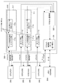
図1は、本発明の実施形態1に係るメモリアクセス制御回路100(MAC)が用いられたデータ処理システムの構成を示すブロック図である。このデータ処理システムは、同図に示すように、メモリアクセス制御回路100、メモリ200、および複数のリクエスタ300(データ処理装置)を備えて構成され、各リクエスタ300は、バス400を介してメモリアクセス制御回路100と接続されている。そして、各リクエスタ300が処理するデータは、メモリ200に格納されてアクセスされるようになっている。すなわち、このデータ処理システムでは、1つのメモリ200の格納領域を複数のリクエスタ300で共有する、いわゆるユニファイドメモリアクセスシステムが構成されている。
(Data processing system configuration)
FIG. 1 is a block diagram showing a configuration of a data processing system using a memory access control circuit 100 (MAC) according to
メモリアクセス制御回路100は、各リクエスタ300のメモリ200に対するアクセス管理(何れのリクエスタに対してメモリ200と入出力を行うかの管理)、およびメモリ200のマッピングの管理(メモリ200の何れのアドレスからデータを入出力するかの管理)を行うハードウェアである。具体的には、メモリアクセス制御回路100は、ある1つのリクエスタ300からアクセス要求(リクエスト)を受け付けると、そのアクセス要求と他のリクエスタ300からのアクセス要求との調停を図り、そのアクセス要求の実行タイミングを決定し、そのリクエストに対する実行タイミングとなった時に、対応する1つのリクエスタ300に対してイネーブル信号ENを発行するようになっている。
The memory
メモリ200は、所定のクロック信号に同期してデータ転送を行うメモリ装置であり、メモリアクセス制御回路100を介して、各リクエスタ300からアクセスされるようになっている。
The
また、メモリ200は、独立して動作させることが可能な複数個のメモリブロック(以下、メモリバンク、または単にバンクと言う。)を備えて構成されている。以下の説明では、メモリ200が4つのメモリバンク(バンクA、バンクB、バンクC、およびバンクD)を備えている例を説明する。
The
また、メモリ200は、外部から供給されるカラムアドレスがプリセットされるカラムアドレスカウンタを備え、このカウンタをメモリ200がインクリメントすることによって、連続的なデータアクセス(バーストアクセス)が行われるようになっている。バーストアクセスが行われる際には、1つのメモリバンクに対しては、一度に一定のサイズ(バースト転送長)のデータ転送が行われる。
In addition, the
このようなメモリ200の例としては、例えばシンクロナスDRAM(Synchronous DRAM)がある。
As an example of such a
リクエスタ300は、例えば、CPU(Central Processing Unit)やDSP(Digital Signal Processor)等のデータ処理装置である。リクエスタ300は、メモリ200にアクセスする場合、すなわち、メモリ200に対して、データの書き込み、またはデータの読み出しを行う場合には、メモリアクセス制御回路100に対してリクエストを発行し、メモリアクセス制御回路100から前記イネーブル信号ENが発行されている間、メモリアクセス制御回路100を介してメモリ200との間でデータの転送(データの書き込みのための転送、またはデータ読み出しのための転送)を行うようになっている。
The
なお、1回のリクエストにともなうデータ転送サイズは、リクエスタ300によって異なっている。例えば、あるリクエスタは、1回のリクエストによって128ワード(ここでは、1ワードは32ビット長のデータとする。)のデータ転送を要求し、また、あるリクエスタは、1回のリクエストによって32ワードのデータ転送を要求する。
Note that the data transfer size associated with one request differs depending on the
また、同一のリクエスタ300から要求されるデータ転送のサイズは、一定でなくてもよい。
Further, the size of data transfer requested from the
(メモリアクセス制御回路100の構成)
上記メモリアクセス制御回路100の構成についてさらに詳しく説明する。
(Configuration of the memory access control circuit 100)
The configuration of the memory
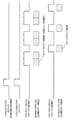
メモリアクセス制御回路100は、図2に示すように、リクエスト分割部110、リクエスト調停部120、およびアクセス制御部130を備えて構成されている。
As shown in FIG. 2, the memory
リクエスト分割部110は、リクエスト分割ブロック111と複数の全バンク単位リクエスト分割部112とを備えて構成されている。各リクエスタ300は、リクエスト分割ブロック111、および全バンク単位リクエスト分割部112の何れかと1対1に対応して接続されている。
The
リクエスト分割ブロック111は、バースト転送長単位リクエスト分割部111aとリクエスト組み立て部111bとを備えて構成されている。
The
バースト転送長単位リクエスト分割部111aは、接続されたリクエスタ300のメモリ200に対するアクセス要求(リクエスト)をバースト転送長単位のアクセス要求に分割して新たなアクセス要求を生成するようになっている。例えば、バースト転送長が4ワードの場合に、リクエスタ300からのアクセス要求が80ワードの転送の要求であれば、新たな20個のアクセス要求が生成される。ただし、一度に転送されるデータが単一のメモリバンク内のデータとなるように、すなわち生成されたそれぞれのアクセス要求が複数のバンクに跨るアクセスにないように、リクエスタ300のアクセス要求の分割が行われるようになっている。
The burst transfer length unit
リクエスト組み立て部111bは、バースト転送長単位リクエスト分割部111aによって分割された複数のアクセス要求を並べ替え、各メモリバンクに対するアクセス要求を1つずつ組み合わせて1つのアクセス要求に組み立てた複数の新たなアクセス要求を生成するようになっている。この組み合わせは、組み立てられたアクセス要求が所定のメモリバンクから順に、全メモリバンク(バンクA〜D)に対し、バーストアクセスが行われるようにされる。
The
また、リクエスト組み立て部111bは、アクセス要求を組み合わせる際に、何れかのメモリバンクに対するアクセス要求が不足している場合には、リクエスタ300に対して、次のリクエストの要求信号を出力し、リクエストがあった場合は、バースト転送長単位リクエスト分割部111aで分割された後、前述同様にリクエスト組み立て部111bでアクセス要求を組み合わせる。
Further, when combining the access requests, the
なお、この場合、同じバンクの要求が重なった場合は、その時点での全バンクの転送でもって、アクセス要求を出力する。なお、何れかのメモリバンクに対するアクセス要求が不足している場合には、不足したアクセス要求を生成して組み合わせるようになっている。 In this case, if requests from the same bank overlap, an access request is output by transferring all banks at that time. Note that when an access request to any of the memory banks is insufficient, an insufficient access request is generated and combined.
バースト転送長単位リクエスト分割部111aとリクエスト組み立て部111bとが上記のように構成されることによって、リクエスト組み立て部111bから出力されるアクセス要求は、バースト転送長が4ワードで、バンク数が4の場合には、16ワード単位のアクセス要求になる。
By configuring the burst transfer length unit
なお、何れのメモリバンクからアクセスが開始されるようにアクセス要求を組み立てるかは、データの格納方法によって決めればよい。例えばメモリ200に画像の1ライン分に相当する連続データの16ワード分が、図3に示すように、4ワード単位でバンクA、B、C、Dの順に格納されている場合には、バンクAからアクセスされるように並べ替えを行う。
It should be noted that which memory bank is used to assemble the access request so that the access is started may be determined by the data storage method. For example, when 16 words of continuous data corresponding to one line of an image are stored in the
全バンク単位リクエスト分割部112は、接続されたリクエスタ300のメモリ200に対するアクセス要求を、全メモリバンクに対しバーストアクセスした場合のデータ転送サイズに分割するようになっている。分割された各アクセス要求における開始バンクは特に規定はなく、各メモリバンクがそれぞれ1つずつ転送されるようになっていればよい。転送時のバンクの順番は全アクセスにおいて一定の順番である。
The all-bank unit
例えばバースト転送長が4ワードで、メモリバンクが4つある場合には、全バンク単位リクエスト分割部112が各リクエスタ300から受け付けたアクセス要求の転送開始位置が0または16N(Nは0または正の整数)で、データ転送のサイズが16m+nワード(mは、0または正の整数、nは、0以上15以下の整数)であったとすれば、図4に示すように、全バンク単位リクエスト分割部112は、アクセス要求を16ワード(4ワード×4=16)ごとのアクセス要求に分割して、それぞれ16ワード分のデータを転送する(m+1)個の新たなアクセス要求(nが0の場合には、m個のアクセス要求)を生成する。
For example, when the burst transfer length is 4 words and there are 4 memory banks, the transfer start position of the access request received from each requester 300 by the all-bank unit
リクエスト調停部120は、リクエスト組み立て部111b、および各全バンク単位リクエスト分割部112によって生成された複数のアクセス要求(何れも16ワードの転送要求)を所定の調停方式に従って並べ替えるようになっている。リクエスト調停部120の調停方式は特に限定されない。
The
アクセス制御部130は、リクエスト調停部120の調停の結果に応じて、アクセス要求をした各リクエスタ300とメモリ200との間のデータ転送の制御を行うようになっている。詳しくは、データを転送するリクエスタ300にイネーブル信号を出力し、メモリ200との間のデータ転送を行う。データ転送は、メモリ200に対しては、リクエスト組み立て部111b、または全バンク単位リクエスト分割部112で生成されたアクセス要求の順番でデータ転送を行うが、各リクエスタ300に対しては、その順番でなくてもかまわない。SDRAMアクセス用に並べ替えはアクセス制御部で行ってもかまわないし、リクエスタへの転送アドレスでもって、制御してもかまわない。
The
(メモリアクセス制御回路100の動作)
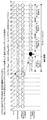
上記のように構成されたメモリアクセス制御回路100の動作をメモリ200にNTSC画像データの1フレーム分が、図5に示すように、16画素単位でバンクA、B、C、Dの順に格納されている場合を例に説明する。この場合、1ワードで4画素分のデータが読み書きできる場合を示す。1画素のデータは1バイト(8ビット)で表されるとする。
なお、画像データはNTSCの場合を例にしている。また、今回のメモリマップ構成は図5に示すように横方向に720画素の有効データが続き、さらに32画素分(2MB分)の未使用領域を含めるとする。この場合、1ライン目のアドレスは、左端から0、1、2、…、15とバンクAに対する領域から始まり、続いて、バンクB、バンクC、バンクDと16画素ずつバンクが切り替わっていく。なお、2ライン目の左端のアドレスは、752となり、バンクD、A、B、Cとなる。以下、同様に最下段の480ライン目まで続く。
(Operation of Memory Access Control Circuit 100)
The operation of the memory
The image data is an example of NTSC. Further, in this memory map configuration, as shown in FIG. 5, it is assumed that valid data of 720 pixels continues in the horizontal direction and an unused area of 32 pixels (2 MB) is included. In this case, the address of the first line starts from 0, 1, 2,..., 15 and the area for the bank A from the left end, and then the bank B, the bank C, and the bank D are switched by 16 pixels. Note that the address at the left end of the second line is 752, and banks D, A, B, and C are provided. Thereafter, the process continues to the bottom line 480.
まず、図6に示すようにMB1の12ライン目、横12画素目から横16画素、縦16画素のデータ転送する場合、リクエスタ300からのリクエストとしては、(1)で示す1ライン分のデータ転送要求が来る。この場合、リクエスト分割部111aでは、バンク毎に分割を行い、バンクC、バンクDのリクエストになる。次にリクエスト組み立て部111bで組み立てを行うが、メモリバンクA、Bに対するリクエストが不足するため、リクエスタ1に対して、リクエスト要求信号を出力し、次のラインに相当する要求(2)をリクエスト分割部111aが受理し、バンクB、Cに分割する。そして、リクエスト組み立て部111bは、バンクB、C、Dのリクエストが貯まり、バンクCが重複するためにバンクB、C、Dのリクエスト1として、リクエスト調停部120に出力する。
First, as shown in FIG. 6, when transferring data of the 12th line of MB1, the horizontal 12 pixels to the horizontal 16 pixels, and the vertical 16 pixels, a request from the
以下、バンクCのみが残り、他のバンクA、B、Dのリクエストが不足するため、リクエスタ1にリクエスト要求信号を出力し、次のラインに相当する要求(3)をリクエスト分割部111aが受理し、バンクA、Bに分割する。そして、リクエスト組み立て部111bは、バンクDのリクエストが不足するために、リクエスタ1にリクエスト要求信号を出力し、次のラインに相当する要求(4)をリクエスト分割部111aが受理し、バンクD、Aに分割する。そして、リクエスト組み立て部111bは、バンクA、B、C、Dのリクエストが貯まり、バンクAが重複するためにバンクA、B、C、Dのリクエスト2として、リクエスト調停部120に出力する。
Hereinafter, since only bank C remains and requests of other banks A, B, and D are insufficient, a request request signal is output to the
以下、同様に16ライン分の転送要求をバンク毎に分割、組み立てを行い、リクエスト1〜9としてDMA(Direct Memory Access)が実行される。
Thereafter, similarly, transfer requests for 16 lines are divided and assembled for each bank, and DMA (Direct Memory Access) is executed as
よって、16ライン分のDMA転送に対して、本来は16回のDMAが必要であったが、この場合は9回のDMAで完了する。 Therefore, 16 DMAs were originally required for the DMA transfer for 16 lines, but in this case, it is completed with 9 DMAs.
上記のように、本実施形態によれば、複数のメモリバンクに格納された2次元データに対し、複数のデータ処理装置が効率的にアクセスすることが可能になる。 As described above, according to this embodiment, a plurality of data processing devices can efficiently access two-dimensional data stored in a plurality of memory banks.
また、各アクセス要求が複数のバンクに跨らないように、メモリに対するアクセス要求を分割し、所定のメモリバンクから順にメモリにアクセスされるように、複数回のリクエストに対し、分割したアクセス要求を並べ替えるので、無効期間(データが出力されない期間)を生じさせないようにできる。 In addition, the access requests for the memory are divided so that each access request does not extend over a plurality of banks, and the divided access requests are divided into a plurality of requests so that the memory is accessed in order from a predetermined memory bank. Since rearrangement is performed, it is possible to prevent an invalid period (a period during which data is not output) from being generated.
《発明の実施形態1の変形例》
なお、実施形態1では、1つのリクエスタ300に対してのみ、リクエスト分割ブロック111が設けられている例を説明したが、例えば図7に示すように複数のリクエスタ300に対して、リクエスト分割ブロック111を設けるようにメモリアクセス制御回路100を構成してもよい。
<< Modification of
In the first embodiment, an example in which the
なお、以下の実施形態や変形例において前記実施形態1等と同様の機能を有する構成要素については、同一の符号を付して説明を省略する。 In the following embodiments and modifications, components having the same functions as those of the first embodiment are denoted by the same reference numerals and description thereof is omitted.
また、リクエスタ300をリクエスト分割部110、および全バンク単位リクエスト分割部112の何れに接続するかは、リクエストの特性に応じて定めればよい。
Whether
《発明の実施形態1の他の変形例》
また、実施形態1の装置において、リクエスタ300から入力された転送回数情報に応じて、複数のアクセス要求をまとめて処理(データ転送)するようにしてもよい。
<< Other Modifications of
In the apparatus according to the first embodiment, a plurality of access requests may be collectively processed (data transfer) according to the transfer count information input from the
発明の実施形態1の他の変形例に係るメモリアクセス制御回路500は、図8に示すようにリクエスト分割部110に代えてリクエスト分割部510を備え、リクエスト調停部120に代えてリクエスト調停部520を備えて構成されている点がメモリアクセス制御回路100と異なっている。
A memory access control circuit 500 according to another modification of the first embodiment of the invention includes a
リクエスト分割部510は、リクエスト分割部110にリクエスト分割ブロック511が追加されている点がリクエスト分割部110と異なっている。
The
リクエスト分割ブロック511は、バースト転送長単位リクエスト分割部111aとリクエスト組み立て部111bとを備え、リクエスタ300から入力された転送回数情報をリクエスト調停部120に出力するようになっている。
The
リクエスト調停部520は、リクエスト分割ブロック111から出力されたアクセス要求が、前記転送回数情報に応じた回数ずつまとめてアクセス制御部130で処理されるように実行順序を調停するようになっている。
The
このように構成されたメモリアクセス制御回路では、例えばリクエスタ300から2回分のアクセスをまとめて処理するように転送回数情報が入力された場合には、バースト転送長単位リクエスト分割部111aとリクエスト組み立て部111bは、リクエスタ300のアクセス要求の分割を行うとともに、前記転送回数情報をリクエスト調停部120に出力する。リクエスト調停部520は、リクエスト分割ブロック111から出力されたアクセス要求が2回分ずつまとめてアクセス制御部130で処理されるように処理順序の調停を行う。そして、これらの要求の処理順になったタイミングでアクセス制御部130からは、図9に示すように、リクエスタ300に対して、イネーブル信号ENが発行され、リクエスタ300とメモリ200の間で、2回分ずつまとめたデータ転送(32ワード分)が行われる。
In the memory access control circuit configured as described above, for example, when transfer count information is input from the requester 300 so as to collectively process two accesses, the burst transfer length unit
なお、全バンク単位リクエスト分割部112に接続されているリクエスタ300からデータ転送の要求があった場合には、16ワード分のデータの転送が行われる。
When there is a data transfer request from the requester 300 connected to the all-bank unit
上記のように本変形例によれば、一度に転送されるデータサイズを制御することができるので、例えば大量のデータを必要とするリクエスタに対しては、一度の処理で転送されるデータサイズの増大を図ることができ、処理速度の向上やデータ転送の効率化を図ることが可能になる。 As described above, according to the present modification, the size of data transferred at a time can be controlled. For example, for a requester that requires a large amount of data, the size of the data transferred at a time is reduced. The increase can be achieved, and the processing speed can be improved and the efficiency of data transfer can be improved.
《発明の実施形態2》
リクエスト調停部で調停の状況(データ転送待ちをしているアクセス要求の数)に応じて、アクセス要求の分割方法を変更するメモリアクセス制御回路の例を説明する。
<<
An example of a memory access control circuit that changes the method for dividing access requests according to the arbitration status (the number of access requests waiting for data transfer) in the request arbitration unit will be described.
本発明の実施形態2に係るメモリアクセス制御回路600は、図10に示すように、実施形態1におけるリクエスト分割部110に代えてリクエスト分割部610を備え、リクエスト調停部120に代えてリクエスト調停部620を備えて構成されている。
As shown in FIG. 10, the memory
リクエスト分割部610は、リクエスト分割ブロック111、リクエスト分割ブロック611、および複数の全バンク単位リクエスト分割部112を備えて構成されている。
The
リクエスト分割ブロック611は、バースト転送長単位リクエスト分割部111a、リクエスト組み立て部111b、全バンク単位リクエスト分割部112、およびリクエスト選択部611cを備えて構成され、リクエスト調停部620の調停の状況(データ転送待ちをしているアクセス要求の数)に応じて、全バンク単位リクエスト分割部112で生成したアクセス要求を出力するか、リクエスト分割ブロック111で生成したアクセス要求を出力するかをリクエスト選択部611cによって切り替えるようになっている。具体的には、データ転送待ちをしているアクセス要求の数が所定の数よりも少ない場合(リクエスト調停部が空いている場合)には、全バンク単位リクエスト分割部112で生成したアクセス要求を出力し、データ転送待ちをしているアクセス要求の数が所定の数よりも多い場合(リクエスト調停部が混んでいる場合)には、リクエスト分割ブロック111で生成したアクセス要求を出力する。
The
リクエスト調停部620は、リクエスト調停部120が有する調停機能に加え、調停状況(データ転送待ちをしているアクセス要求の数)をリクエスト分割部610に出力するように構成される。
The
上記の構成により、例えば全バンク単位リクエスト分割部112によって生成されたアクセス要求が出力された場合には、実施形態1で説明したように、リクエスト回数が増える場合があるが、リクエスト組み立て部111bにおける組み立てにかかる時間を省くことが可能になるので、リクエスト調停部が空いていれば、転送速度を重視したデータ転送が可能になる。
With the above configuration, for example, when the access request generated by the all-bank unit
一方、リクエスト調停部が混んでいる場合には、リクエスト分割ブロック111によって生成されたアクセス要求が出力されることによって、無駄なリクエストが削減されるとともに、無効期間(データが出力されない期間)を生じさせないようにできるので、転送効率の改善が可能になる。
On the other hand, when the request arbitration unit is crowded, the access request generated by the
上記のように本実施形態によれば、リクエスト調停状況に応じて、アクセス要求の分割方法を変更できるので、処理速度の向上やデータ転送の効率化を図ることが可能になる。 As described above, according to the present embodiment, since the access request division method can be changed according to the request arbitration status, the processing speed can be improved and the data transfer efficiency can be improved.
《発明の実施形態2の変形例》
リクエスト調停部120の調停の状況に応じてアクセス要求の分割方法を変更するのではなく、リクエスタ300から与えられた転送要求時間信号が示す転送要求時間(データ処理装置がデータ転送要求を出力してからデータ転送が開始されるべき時間)に応じて、アクセス要求の分割方法を変更するようにしてもよい。具体的には図11に示すように、リクエスタ300が出力する前記転送要求時間信号が入力されるように、リクエスト分割ブロック611を構成する。
<< Modification of
Rather than changing the method of dividing the access request according to the arbitration status of the
また、リクエスタ300から入力されたが示す転送要求時間が所定の時間以下の場合には、全バンク単位リクエスト分割部112で生成したアクセス要求を出力し、前記転送要求時間が所定の時間よりも長い場合には、リクエスト組み立て部111bで組み立てたアクセス要求を出力するように、リクエスト選択部611cを構成する。
When the transfer request time indicated by the
これにより、転送要求時間に応じて、アクセス要求の分割方法を選択することができ、処理速度の向上やデータ転送の効率化を図ることが可能になる。 As a result, it is possible to select an access request dividing method according to the transfer request time, and it is possible to improve the processing speed and increase the efficiency of data transfer.
《発明の実施形態2の他の変形例》
また、リクエスタ300から出力された分割要求信号に応じて、アクセス要求の分割方法を変更するようにしてもよい。具体的には、図12に示すようにリクエスタ300から入力された分割要求信号に応じて、全バンク単位リクエスト分割部112で生成したアクセス要求、およびリクエスト分割ブロック111で生成したアクセス要求のうちの何れかを選択的に出力するようにリクエスト選択部611cを構成すればよい。
<< Other Modifications of
Further, the access request dividing method may be changed in accordance with the division request signal output from the
これにより、ソフト制御によりアクセス要求の分割方法を制御することが可能となり、例えば転送するデータの読み込み開始位置やデータの種類に応じて、分割方法を制御すれば、処理速度の向上やデータ転送の効率化を図ることが可能になる。 This makes it possible to control the dividing method of access requests by software control. For example, if the dividing method is controlled according to the reading start position of the data to be transferred and the type of data, the processing speed can be improved and Efficiency can be improved.
なお、上記の各実施形態で示したデータ語長の単位は特定のワード長に限定されず、例えばバイト(8ビット)、ロングワード(32ビット)等であってもよい。 The unit of the data word length shown in the above embodiments is not limited to a specific word length, and may be, for example, a byte (8 bits), a long word (32 bits), or the like.
また、同期型メモリはSDRAMに限定されず、例えば、シンクロナスSRAM等のクロック同期型のメモリであってもよい。 The synchronous memory is not limited to the SDRAM, and may be a clock synchronous memory such as a synchronous SRAM, for example.
また、リクエスト分割ブロック111や全バンク単位リクエスト分割部112の数も例示であり、データ処理装置の数などに応じて、必要な数だけリクエスト分割ブロック111等を設ければよい。
The number of request division blocks 111 and all-bank unit
また、上記の各実施形態では、転送されるデータが画像データの例を説明したが、連続的なデータとしてはこれには限定されず、例えば音声データ等であってもよい。 In each of the above-described embodiments, the example in which the data to be transferred is image data has been described. However, the continuous data is not limited thereto, and may be audio data, for example.
本発明にかかるメモリアクセス制御回路は、複数のメモリバンクに格納された2次元データに対し、データ処理装置が効率的にアクセスを行うことが可能になるという効果を有し、データ処理装置による同期型メモリに対するアクセス動作を制御するメモリアクセス制御回路等として有用である。 The memory access control circuit according to the present invention has an effect that the data processing apparatus can efficiently access two-dimensional data stored in a plurality of memory banks. This is useful as a memory access control circuit for controlling an access operation to a type memory.
100 メモリアクセス制御回路
110 リクエスト分割部
111 リクエスト分割ブロック
111a バースト転送長単位リクエスト分割部
111b リクエスト組み立て部
112 全バンク単位リクエスト分割部
120 リクエスト調停部
130 アクセス制御部
200 メモリ
300 リクエスタ
400 バス
500 メモリアクセス制御回路
510 リクエスト分割部
511 リクエスト分割ブロック
520 リクエスト調停部
600 メモリアクセス制御回路
610 リクエスト分割部
611 リクエスト分割ブロック
611c リクエスト選択部
620 リクエスト調停部
DESCRIPTION OF
Claims (8)
前記メモリは、独立して動作させることが可能な複数個のメモリバンクを有し、クロック信号に同期してデータをバースト転送することが可能な同期型メモリであり、
前記メモリに対する第1のデータ転送要求を前記データ処理装置から受け付けるとともに、受け付けた第1のデータ転送要求を、データ転送量が一度にバースト転送されるデータ量で、一度に転送されるデータが単一のメモリバンク内のデータである複数のデータ転送要求に分割するバースト転送長単位転送要求分割部と、
前記バースト転送長単位転送要求分割部が分割した複数のデータ転送要求を、各メモリバンクに対するデータ転送要求が1つずつ組み合わせられたデータ転送要求に組み立てて、複数の新たなデータ転送要求を生成する転送要求組み立て部と、
前記新たなデータ転送要求に基づいて、前記メモリと前記データ処理装置との間のデータ転送を制御するデータ転送制御部とを備え、
前記転送要求組み立て部は、データ転送要求を組み合わせる際に、何れかのメモリバンクに対するデータ転送要求が不足している場合には、前記バースト転送長単位転送要求分割部に、前記データ処理装置から第2のデータ転送要求または複数のデータ転送要求の受け付け、および前記分割処理をさせるとともに、分割されたデータ転送要求を組み合わせて、不足したメモリバンクに対するデータ転送要求を生成するように構成されていることを特徴とするメモリアクセス制御回路。 A memory access control circuit for controlling access to a memory by a data processing device,
The memory has a plurality of memory banks that can be operated independently, and is a synchronous memory capable of burst-transferring data in synchronization with a clock signal,
The first data transfer request for the memory is received from the data processing device, and the received first data transfer request is received at a single data transfer amount with a data transfer amount of burst transfer at a time. A burst transfer length unit transfer request dividing unit for dividing a plurality of data transfer requests that are data in one memory bank;
A plurality of data transfer requests divided by the burst transfer length unit transfer request dividing unit are assembled into data transfer requests in which data transfer requests for each memory bank are combined one by one, and a plurality of new data transfer requests are generated. A transfer request assembly unit;
A data transfer control unit for controlling data transfer between the memory and the data processing device based on the new data transfer request;
When the data transfer request for any of the memory banks is insufficient when combining the data transfer requests, the transfer request assembling unit sends the burst transfer length unit transfer request dividing unit from the data processing device to the burst transfer length unit transfer request dividing unit. The second data transfer request or the plurality of data transfer requests are accepted and the dividing process is performed, and the divided data transfer requests are combined to generate a data transfer request for the insufficient memory bank. A memory access control circuit.
前記転送要求組み立て部は、分割された、第1のデータ転送要求、第2のデータ転送要求、または複数のデータ転送要求を組み合わせる際に、何れかのメモリバンクに対するデータ転送要求が不足している場合かつ同一のメモリバンクに対するデータ転送要求が複数ある場合には、不足したデータ転送要求を生成して組み合わせるように構成されていることを特徴とするメモリアクセス制御回路。 The memory access control circuit according to claim 1,
When the transfer request assembly unit combines the divided first data transfer request, second data transfer request, or a plurality of data transfer requests, the data transfer request for any memory bank is insufficient. A memory access control circuit configured to generate and combine deficient data transfer requests when there are a plurality of data transfer requests for the same memory bank.
前記バースト転送長単位転送要求分割部、および転送要求組み立て部は、少なくともそれぞれ2つ以上設けられ、
さらに、各転送要求組み立て部が生成したデータ転送要求の実行順序を決定する実行順序決定部を備え、
前記データ転送制御部は、前記実行順序決定部が決定した順序でデータ転送を制御するように構成されていることを特徴とするメモリアクセス制御回路。 A memory access control circuit according to any one of claims 1 and 2,
At least two burst transfer length unit transfer request dividing units and transfer request assembling units are provided,
Furthermore, an execution order determination unit that determines the execution order of the data transfer requests generated by each transfer request assembly unit,
The memory access control circuit, wherein the data transfer control unit is configured to control data transfer in an order determined by the execution order determining unit.
前記バースト転送長単位転送要求分割部によってデータ転送要求が受け付けられるデータ処理装置とは互いに異なるデータ処理装置から前記メモリに対するデータ転送要求を受け付けるとともに、受け付けたデータ転送要求を、データ転送量が、一度にバースト転送されるデータ量と前記メモリが有するメモリバンクの数との乗算値であるデータ転送要求に分割して複数の新たなデータ転送要求を生成する全メモリバンク単位転送要求分割部と、
前記転送要求組み立て部が生成したデータ転送要求、および前記全メモリバンク単位転送要求分割部が生成したデータ転送要求の実行順序を決定する実行順序決定部とを備え、
前記データ転送制御部は、前記実行順序決定部が決定した順序でデータ転送を制御するように構成されていることを特徴とするメモリアクセス制御回路。 A memory access control circuit according to any one of claims 1 and 2, further comprising:
The data transfer request for the memory is received from a data processing device different from the data processing device from which the data transfer request is received by the burst transfer length unit transfer request dividing unit. An all-memory bank unit transfer request dividing unit that generates a plurality of new data transfer requests by dividing the data transfer request into a data transfer request that is a multiplication value of the amount of data burst-transferred and the number of memory banks included in the memory;
A data transfer request generated by the transfer request assembling unit, and an execution order determining unit that determines an execution order of the data transfer request generated by the all memory bank unit transfer request dividing unit,
The memory access control circuit, wherein the data transfer control unit is configured to control data transfer in an order determined by the execution order determining unit.
前記実行順序決定部は、データ処理装置から与えられた回数情報が示す回数だけ連続して、当該データ処理装置のデータ転送要求が実行されるように実行順序を決定するように構成されていることを特徴とするメモリアクセス制御回路。 A memory access control circuit according to any one of claims 3 and 4,
The execution order determination unit is configured to determine the execution order so that the data transfer request of the data processing device is executed continuously for the number of times indicated by the number of times information given from the data processing device. A memory access control circuit.
前記バースト転送長単位転送要求分割部と同じデータ転送要求を受け付けるとともに、受け付けたデータ転送要求を、データ転送量が、一度にバースト転送されるデータ量と前記メモリバンクの数との乗算値であるデータ転送要求に分割して複数の新たなデータ転送要求を生成する全メモリバンク単位転送要求分割部と、
データ転送が終了していないデータ転送要求がいくつあるかを示す転送状況情報が入力され、前記転送状況情報が示すデータ転送待ちのデータ転送要求の数が所定数よりも少ない場合には、前記全メモリバンク単位転送要求分割部が生成したデータ転送要求を実行順序決定部に出力し、データ転送待ちのデータ転送要求の数が所定数よりも多い場合には、前記転送要求組み立て部が生成したデータ転送要求を実行順序決定部に出力する選択部とを備え、
前記実行順序決定部は、入力されたデータ転送要求の実行順序を決定する一方、前記転送状況情報を出力するように構成されていることを特徴とするメモリアクセス制御回路。 A memory access control circuit according to any one of claims 3 and 4, further comprising:
The same data transfer request as the burst transfer length unit transfer request dividing unit is received, and the received data transfer request is a product of the data transfer amount and the number of memory banks that are burst transferred at a time. An all memory bank unit transfer request dividing unit that generates a plurality of new data transfer requests by dividing into data transfer requests;
When transfer status information indicating how many data transfer requests have not been transferred is input and the number of data transfer requests waiting for data transfer indicated by the transfer status information is less than a predetermined number, The data transfer request generated by the memory bank unit transfer request dividing unit is output to the execution order determining unit, and when the number of data transfer requests waiting for data transfer is greater than a predetermined number, the data generated by the transfer request assembling unit A selection unit that outputs the transfer request to the execution order determination unit,
The memory access control circuit, wherein the execution order determination unit is configured to output the transfer status information while determining an execution order of input data transfer requests.
前記バースト転送長単位転送要求分割部と同じデータ転送要求を受け付けるとともに、受け付けたデータ転送要求を、データ転送量が、一度にバースト転送されるデータ量と前記メモリバンクの数との乗算値であるデータ転送要求に分割して複数の新たなデータ転送要求を生成する全メモリバンク単位転送要求分割部と、
前記データ処理装置がデータ転送要求を出力してからどれくらいの転送要求時間内にデータ転送が開始されるべきかを示す転送要求時間情報が前記データ処理装置から入力され、前記転送要求時間情報が示す転送要求時間が所定の時間よりも短い場合には、前記全メモリバンク単位転送要求分割部が生成したデータ転送要求を実行順序決定部に出力し、前記転送要求時間が所定の時間よりも長い場合には、前記転送要求組み立て部が生成したデータ転送要求を実行順序決定部に出力する選択部と、
を備えたことを特徴とするメモリアクセス制御回路。 A memory access control circuit according to any one of claims 1 and 2, further comprising:
The same data transfer request as that of the burst transfer length unit transfer request dividing unit is received, and the received data transfer request is a product of the data transfer amount multiplied by the amount of data to be burst transferred at one time and the number of the memory banks. An all memory bank unit transfer request dividing unit that generates a plurality of new data transfer requests by dividing into data transfer requests;
Transfer request time information indicating how long the data transfer should be started after the data processing device outputs the data transfer request is input from the data processing device, and the transfer request time information indicates When the transfer request time is shorter than the predetermined time, the data transfer request generated by the all memory bank unit transfer request dividing unit is output to the execution order determining unit, and the transfer request time is longer than the predetermined time. A selection unit that outputs the data transfer request generated by the transfer request assembly unit to the execution order determination unit;
A memory access control circuit comprising:
前記バースト転送長単位転送要求分割部と同じデータ転送要求を受け付けるとともに、受け付けたデータ転送要求を、データ転送量が、一度にバースト転送されるデータ量と前記メモリバンクの数との乗算値であるデータ転送要求に分割して複数の新たなデータ転送要求を生成する全メモリバンク単位転送要求分割部と、
前記データ処理装置が出力する選択情報に基づいて、前記全メモリバンク単位転送要求分割部が生成したデータ転送要求、および前記転送要求組み立て部が生成したデータ転送要求の何れか一方を選択的に出力する選択部と、
を備えたことを特徴とするメモリアクセス制御回路。
A memory access control circuit according to any one of claims 1 and 2, further comprising:
The same data transfer request as that of the burst transfer length unit transfer request dividing unit is received, and the received data transfer request is a product of the data transfer amount multiplied by the amount of data to be burst transferred at one time and the number of the memory banks. An all memory bank unit transfer request dividing unit that generates a plurality of new data transfer requests by dividing into data transfer requests;
Based on the selection information output by the data processing device, selectively outputs either the data transfer request generated by the all memory bank unit transfer request dividing unit or the data transfer request generated by the transfer request assembling unit A selection section to
A memory access control circuit comprising:
Priority Applications (1)
| Application Number | Priority Date | Filing Date | Title |
|---|---|---|---|
| JP2005198625A JP2007018222A (en) | 2005-07-07 | 2005-07-07 | Memory access control circuit |
Applications Claiming Priority (1)
| Application Number | Priority Date | Filing Date | Title |
|---|---|---|---|
| JP2005198625A JP2007018222A (en) | 2005-07-07 | 2005-07-07 | Memory access control circuit |
Publications (1)
| Publication Number | Publication Date |
|---|---|
| JP2007018222A true JP2007018222A (en) | 2007-01-25 |
Family
ID=37755349
Family Applications (1)
| Application Number | Title | Priority Date | Filing Date |
|---|---|---|---|
| JP2005198625A Withdrawn JP2007018222A (en) | 2005-07-07 | 2005-07-07 | Memory access control circuit |
Country Status (1)
| Country | Link |
|---|---|
| JP (1) | JP2007018222A (en) |
Cited By (6)
| Publication number | Priority date | Publication date | Assignee | Title |
|---|---|---|---|---|
| JP2009534863A (en) * | 2006-04-25 | 2009-09-24 | コーニンクレッカ フィリップス エレクトロニクス エヌ ヴィ | Fluorescent lighting that produces white light |
| US8171222B2 (en) | 2008-07-24 | 2012-05-01 | Sony Corporation | Memory access system, memory control apparatus, memory control method and program |
| US8748515B2 (en) | 2010-04-15 | 2014-06-10 | Henry Company Llc | Mixtures and emulsions for use in providing strength to gypsum compositions |
| US9045370B2 (en) | 2011-02-24 | 2015-06-02 | Henry Company Llc | Aqueous wax emulsions having reduced solids content for use in gypsum compositions and building products |
| JP2015225458A (en) * | 2014-05-27 | 2015-12-14 | 京セラドキュメントソリューションズ株式会社 | Information processing device and arbitration method |
| JP2021015465A (en) * | 2019-07-12 | 2021-02-12 | 日本エイ・ティー・エム株式会社 | Watching service system |
-
2005
- 2005-07-07 JP JP2005198625A patent/JP2007018222A/en not_active Withdrawn
Cited By (7)
| Publication number | Priority date | Publication date | Assignee | Title |
|---|---|---|---|---|
| JP2009534863A (en) * | 2006-04-25 | 2009-09-24 | コーニンクレッカ フィリップス エレクトロニクス エヌ ヴィ | Fluorescent lighting that produces white light |
| US8171222B2 (en) | 2008-07-24 | 2012-05-01 | Sony Corporation | Memory access system, memory control apparatus, memory control method and program |
| US8748515B2 (en) | 2010-04-15 | 2014-06-10 | Henry Company Llc | Mixtures and emulsions for use in providing strength to gypsum compositions |
| US9045370B2 (en) | 2011-02-24 | 2015-06-02 | Henry Company Llc | Aqueous wax emulsions having reduced solids content for use in gypsum compositions and building products |
| JP2015225458A (en) * | 2014-05-27 | 2015-12-14 | 京セラドキュメントソリューションズ株式会社 | Information processing device and arbitration method |
| JP2021015465A (en) * | 2019-07-12 | 2021-02-12 | 日本エイ・ティー・エム株式会社 | Watching service system |
| JP7171521B2 (en) | 2019-07-12 | 2022-11-15 | SocioFuture株式会社 | Monitoring service system |
Similar Documents
| Publication | Publication Date | Title |
|---|---|---|
| JP4820566B2 (en) | Memory access control circuit | |
| US7668040B2 (en) | Memory device, memory controller and memory system | |
| JP4786209B2 (en) | Memory access device | |
| US7814294B2 (en) | Memory device, memory controller and memory system | |
| US6104417A (en) | Unified memory computer architecture with dynamic graphics memory allocation | |
| US8095744B2 (en) | Device for controlling access from a plurality of masters to shared memory composed of a plurality of banks each having a plurality of pages | |
| JP5351145B2 (en) | Memory control device, memory system, semiconductor integrated circuit, and memory control method | |
| JP4416694B2 (en) | Data transfer arbitration device and data transfer arbitration method | |
| US20110078351A1 (en) | Information processor system | |
| JP2007018222A (en) | Memory access control circuit | |
| US7096312B2 (en) | Data transfer device and method for multidimensional memory | |
| WO2009116115A1 (en) | Memory controller and memory system using the same | |
| US20110087821A1 (en) | Apparatus to access multi-bank memory | |
| JP2003186740A (en) | Memory control device and memory control method | |
| US6374244B1 (en) | Data transfer device | |
| JP2001125826A (en) | Device provided with plural processors having interface for set memory | |
| JP6294732B2 (en) | Data transfer control device and memory built-in device | |
| US8099530B2 (en) | Data processing apparatus | |
| JPH10144073A (en) | Access mechanism for synchronous dram | |
| US20100030978A1 (en) | Memory controller, memory control method, and image processing device | |
| JP2003271445A (en) | Memory control device and method | |
| US6785795B1 (en) | Data processing device for use in cooperation with a memory | |
| JP2002182975A (en) | Multi-processor system | |
| JPH09120371A (en) | Memory controller | |
| JP2000029777A (en) | Data transfer device |
Legal Events
| Date | Code | Title | Description |
|---|---|---|---|
| A621 | Written request for application examination |
Free format text: JAPANESE INTERMEDIATE CODE: A621 Effective date: 20080115 |
|
| A761 | Written withdrawal of application |
Free format text: JAPANESE INTERMEDIATE CODE: A761 Effective date: 20090310 |