JP2006505128A - Plasma treatment magnetically enhanced by high power pulses - Google Patents

Plasma treatment magnetically enhanced by high power pulses Download PDF

Info

Publication number
JP2006505128A
JP2006505128A JP2004548534A JP2004548534A JP2006505128A JP 2006505128 A JP2006505128 A JP 2006505128A JP 2004548534 A JP2004548534 A JP 2004548534A JP 2004548534 A JP2004548534 A JP 2004548534A JP 2006505128 A JP2006505128 A JP 2006505128A
Authority
JP
Japan
Prior art keywords
cathode
ionized plasma
plasma
substrate
ions
Prior art date
Legal status (The legal status is an assumption and is not a legal conclusion. Google has not performed a legal analysis and makes no representation as to the accuracy of the status listed.)
Withdrawn
Application number
JP2004548534A
Other languages
Japanese (ja)
Inventor
ローマン チストヤコブ,
Original Assignee
ゾンド, インコーポレイテッド
Priority date (The priority date is an assumption and is not a legal conclusion. Google has not performed a legal analysis and makes no representation as to the accuracy of the date listed.)
Filing date
Publication date
Family has litigation
First worldwide family litigation filed litigation Critical https://patents.darts-ip.com/?family=32106072&utm_source=google_patent&utm_medium=platform_link&utm_campaign=public_patent_search&patent=JP2006505128(A) "Global patent litigation dataset” by Darts-ip is licensed under a Creative Commons Attribution 4.0 International License.
Application filed by ゾンド, インコーポレイテッド filed Critical ゾンド, インコーポレイテッド
Publication of JP2006505128A publication Critical patent/JP2006505128A/en
Withdrawn legal-status Critical Current

Links

Images

Classifications

    • HELECTRICITY
    • H01ELECTRIC ELEMENTS
    • H01JELECTRIC DISCHARGE TUBES OR DISCHARGE LAMPS
    • H01J37/00Discharge tubes with provision for introducing objects or material to be exposed to the discharge, e.g. for the purpose of examination or processing thereof
    • H01J37/32Gas-filled discharge tubes
    • H01J37/32431Constructional details of the reactor
    • H01J37/3266Magnetic control means
    • HELECTRICITY
    • H01ELECTRIC ELEMENTS
    • H01JELECTRIC DISCHARGE TUBES OR DISCHARGE LAMPS
    • H01J37/00Discharge tubes with provision for introducing objects or material to be exposed to the discharge, e.g. for the purpose of examination or processing thereof
    • H01J37/32Gas-filled discharge tubes
    • H01J37/32431Constructional details of the reactor
    • H01J37/32697Electrostatic control
    • H01J37/32706Polarising the substrate

Abstract

Magnetically enhanced plasma processing methods and apparatus are described. A magnetically enhanced plasma processing apparatus according to the present invention includes an anode and a cathode that is positioned adjacent to the anode. An ionization source generates a weakly-ionized plasma proximate to the cathode. A magnet is positioned to generate a magnetic field proximate to the weakly-ionized plasma. The magnetic field substantially traps electrons in the weakly-ionized plasma proximate to the cathode. A power supply produces an electric field in a gap between the anode and the cathode. The electric field generates excited atoms in the weakly-ionized plasma and generates secondary electrons from the cathode. The secondary electrons ionize the excited atoms, thereby creating a strongly-ionized plasma. A voltage supply applies a bias voltage to a substrate that is positioned proximate to the cathode that causes ions in the plurality of ions to impact a surface of the substrate in a manner that causes etching of the surface of the substrate

Description

プラズマ処理は、半導体製造産業などの多くの産業において広く用いられている。例えば、プラズマエッチングは、半導体製造産業において広く用いられている。表面から材料を除去するために用いられるプラズマエッチング処理には、スパッタエッチング、純化学的エッチング(pure chemical etching)、イオンエネルギー誘起エッチング(ion energy driven etching)、および、イオンインヒビターエッチング(ion inhibitor etching)の4つの基本的な典型がある。   Plasma processing is widely used in many industries such as the semiconductor manufacturing industry. For example, plasma etching is widely used in the semiconductor manufacturing industry. Plasma etching processes used to remove material from the surface include sputter etching, pure chemical etching, ion energy induced etching, and ion inhibitor etching. There are four basic typologies:

スパッタエッチングでは、高エネルギーイオンの衝撃により、基板の表面から原子を取り出す。純化学的エッチングでは、プラズマ放電を用いることにより、ガス相のエッチャント原子を供給し、そのエッチャント原子は、基板の表面と化学的に反応することにより、ガス相の生成物を形成する。イオン強化エネルギー誘起エッチングでは、プラズマ放電を用いることにより、エッチャントおよび高エネルギーのイオンを基板の表面に供給する。イオンインヒビターエッチングでは、放電を用いることにより、エッチャント、高エネルギーのイオン、および、インヒビター前駆体分子を供給し、そのインヒビター前駆体分子が、基板に堆積することにより、保護層フィルムを形成する。周知のスパッタエッチングシステムの均一性およびエッチング速度を高めることは望ましい。   In sputter etching, atoms are extracted from the surface of the substrate by impact of high energy ions. In pure chemical etching, gas phase etchant atoms are supplied by using plasma discharge, and the etchant atoms chemically react with the surface of the substrate to form a gas phase product. In ion-enhanced energy-induced etching, an etchant and high-energy ions are supplied to the surface of the substrate by using plasma discharge. In ion inhibitor etching, an etchant, high-energy ions, and inhibitor precursor molecules are supplied by using discharge, and the inhibitor precursor molecules are deposited on a substrate to form a protective layer film. It is desirable to increase the uniformity and etch rate of known sputter etching systems.

本発明は、特に、詳細な説明において記載される。添付の図面とともに以下の記載を参照することによって、本発明の上記の利点およびさらなる利点はより良く理解され得る。図面において、類似した数字は、様々な図における類似した構造要素および特徴を示す。図面は必ずしもその縮尺である必要はなく、本発明の原理の図示を重視したものである。   The invention is particularly described in the detailed description. The above and further advantages of the present invention may be better understood by referring to the following description in conjunction with the accompanying drawings. In the drawings, like numerals indicate like structural elements and features in the various drawings. The drawings are not necessarily to scale, emphasizing the principles of the invention.

(詳細な説明)
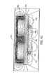
図1は、無線周波数(RF)電源102を有する周知の磁気強化エッチング装置100の断面図を示す。周知の磁気強化エッチング装置100には、プラズマ105を閉じ込めるための真空チャンバ104が含まれる。真空ポンプ106は、管108を介して真空チャンバ104と流動的に結合される。真空ポンプ106は、真空チャンバ104を高真空に真空引きし、そのチャンバをプラズマ処理に適する圧力に保つように適合される。アルゴンガス供給源などのガス供給源109は、ガス注入口110を介して真空チャンバ104にガスを導入する。バルブ112は、チャンバ104へのガス流量を制御する。
(Detailed explanation)
FIG. 1 shows a cross-sectional view of a known magnetic enhanced etching apparatus 100 having a radio frequency (RF) power supply 102. The known magnetically enhanced etching apparatus 100 includes a vacuum chamber 104 for confining a plasma 105. The vacuum pump 106 is fluidly coupled to the vacuum chamber 104 via a tube 108. The vacuum pump 106 is adapted to evacuate the vacuum chamber 104 to a high vacuum and maintain the chamber at a pressure suitable for plasma processing. A gas supply source 109 such as an argon gas supply source introduces gas into the vacuum chamber 104 via the gas inlet 110. Valve 112 controls the gas flow rate into chamber 104.

磁気強化エッチング装置100にはカソード114も含まれる。カソード114は、通常、円板の形をした電極である。カソード114は、伝送線122によって、ブロッキングコンデンサ120の第1の電極118に電気接続される。ブロッキングコンデンサ120の第2の電極124は、RF電源102の第1の出力126に結合される。絶縁体128は、真空チャンバ104の壁に伝送線122を貫通させるために用いられるが、絶縁体128によって、カソード114を真空チャンバ104と絶縁させる。   The magnetic enhanced etching apparatus 100 also includes a cathode 114. The cathode 114 is usually an electrode in the form of a disc. The cathode 114 is electrically connected to the first electrode 118 of the blocking capacitor 120 by the transmission line 122. The second electrode 124 of the blocking capacitor 120 is coupled to the first output 126 of the RF power source 102. The insulator 128 is used to penetrate the transmission line 122 through the wall of the vacuum chamber 104. The insulator 128 insulates the cathode 114 from the vacuum chamber 104.

アノード130は、真空チャンバ104においてカソード114の反対側に配置される。アノード130は、送電線132によってグランドに電気的に結合される。RF電源102の第2の出力134もグランドに電気的に結合される。絶縁体136を用いることにより、真空チャンバ104の壁に送電線132を貫通させて、アノード130を真空チャンバ104と絶縁する。真空チャンバ104は、グランドにも電気的に結合され得る。   The anode 130 is disposed on the opposite side of the cathode 114 in the vacuum chamber 104. Anode 130 is electrically coupled to ground by power transmission line 132. The second output 134 of the RF power supply 102 is also electrically coupled to ground. By using the insulator 136, the power transmission line 132 passes through the wall of the vacuum chamber 104 to insulate the anode 130 from the vacuum chamber 104. The vacuum chamber 104 can also be electrically coupled to ground.

カソード114の上面に実質的に平行な方向に磁場142を発生させるために、一対の磁石140をチャンバ104の外部に配置させる。カソード114の上に基板144を配置させる。   In order to generate the magnetic field 142 in a direction substantially parallel to the upper surface of the cathode 114, a pair of magnets 140 are disposed outside the chamber 104. A substrate 144 is disposed on the cathode 114.

動作中に、後にエッチングされる基板144をカソード114の上に配置させる。真空ポンプ106を用いて、チャンバ104を高真空に十分真空引きする。ガス注入口110を介して、ガス供給源109からチャンバ104にエッチングガスを導入する。RF電源102は、ブロッキングコンデンサ120を介してカソード114に、13.56MHzの高周波数の放射線を提供する。   In operation, a substrate 144 to be etched later is placed over the cathode 114. The chamber 104 is sufficiently evacuated to a high vacuum by using the vacuum pump 106. An etching gas is introduced into the chamber 104 from the gas supply source 109 through the gas inlet 110. The RF power supply 102 provides high frequency radiation at 13.56 MHz to the cathode 114 via the blocking capacitor 120.

カソード114に提供される高周波数の放射線によって、カソード114の上面に垂直な方向に高周波数の電場146が作り出される。磁場142と、高周波数の電場146とは、基板144の上の領域148おいて、交差する。電子は領域148内に閉じ込められ、エッチングガスからの中性原子と衝突する。その衝突によって、高密度のプラズマ105が生成される。負のバイアスがかけられたカソード114は、プラズマ105中の正に帯電したイオンを十分に加速して引き付ける。それによって、イオンは基板144の表面をエッチングする。   The high frequency radiation provided to the cathode 114 creates a high frequency electric field 146 in a direction perpendicular to the top surface of the cathode 114. The magnetic field 142 and the high frequency electric field 146 intersect in a region 148 on the substrate 144. The electrons are confined in region 148 and collide with neutral atoms from the etching gas. Due to the collision, a high-density plasma 105 is generated. The negatively biased cathode 114 sufficiently accelerates and attracts positively charged ions in the plasma 105. Thereby, the ions etch the surface of the substrate 144.

カソード114とアノード130との間に印加されるRF電力は、真空チャンバ104においてエッチングガスを電離し、プラズマ105を作り出すに十分な大きさである。プラズマは、正のイオンと負の電子とから成る。典型的なRF駆動電圧は、500V〜5000Vの間にあり、カソード114とアノード130との間隔138は、約70mmである。典型的な圧力は、10mTorr〜100mTorrの範囲にある。典型的な電力密度は、0.1W/cm〜1W/cmの範囲にある。典型的なプラズマ密度は、10cm−3〜1011cm−3であり、電子温度は、3eVのオーダーである。 The RF power applied between the cathode 114 and the anode 130 is large enough to ionize the etching gas in the vacuum chamber 104 and create the plasma 105. The plasma consists of positive ions and negative electrons. A typical RF drive voltage is between 500V and 5000V, and the spacing 138 between the cathode 114 and the anode 130 is about 70 mm. Typical pressures are in the range of 10 mTorr to 100 mTorr. Typical power densities are in the range of 0.1W / cm 2 ~1W / cm 2 . The typical plasma density is 10 9 cm −3 to 10 11 cm −3 and the electron temperature is on the order of 3 eV.

スパッタエッチング用のプラズマ105を生成する電離プロセスは、電子衝突による直接電離または原子電離と呼ばれることもあり、次のように記述し得る。   The ionization process for generating the plasma 105 for sputter etching is sometimes called direct ionization or atomic ionization by electron impact, and can be described as follows.

Ar+e→Ar+2e
ここで、Arは、エッチングガス中の中性のアルゴン原子を表し、eは、カソード114とアノード130との間に印加される電圧に応答して生成されるイオン化用電子を表す。中性のアルゴン原子とイオン化用電子との衝突によって、アルゴンイオン(Ar)と2つの電子が得られる。
Ar + e → Ar + + 2e
Here, Ar represents neutral argon atoms in the etching gas, and e represents ionization electrons generated in response to a voltage applied between the cathode 114 and the anode 130. Argon ions (Ar + ) and two electrons are obtained by collision between neutral argon atoms and ionizing electrons.

カソード114からの二次電子放出によって、プラズマ放電は保持される。しかし、典型的な動作圧力が比較的高い必要があるために、二次電子はアノード130またはチャンバ104の壁から離れない。プラズマエッチングを含めた大抵のプラズマ処理において、このような圧力は最適ではない。   The plasma discharge is maintained by secondary electron emission from the cathode 114. However, secondary electrons do not leave the anode 130 or the walls of the chamber 104 because the typical operating pressure needs to be relatively high. In most plasma processes, including plasma etching, such pressure is not optimal.

電離を引き起こす電子は、一般的には、磁石140により作り出される磁場に閉じ込められる。磁場閉じ込めは、磁力線が電極の表面に平行な閉じ込め領域148において最も強い。一般的に、閉じ込め領域148におけるプラズマ内の正に帯電したイオンの濃度は、チャンバ104内のどの領域におけるその濃度よりも高い。従って、基板144は、正に帯電したイオンの濃度がより高い領域の近傍領域において、より速くエッチングされる。その領域における速いエッチングによって、望ましくない基板144の不均一なエッチングが得られる。   The electrons that cause ionization are typically confined to the magnetic field created by the magnet 140. Magnetic field confinement is strongest in a confinement region 148 where the magnetic field lines are parallel to the surface of the electrode. In general, the concentration of positively charged ions in the plasma in the confinement region 148 is higher than its concentration in any region in the chamber 104. Accordingly, the substrate 144 is etched faster in the vicinity of the region where the concentration of positively charged ions is higher. Fast etching in that region results in undesirable non-uniform etching of the substrate 144.

プラズマに印加するRF電力を激増することだけでは、エッチングの均一性を改善するより均一でより密度の高いプラズマの形成は得られない。磁場が電極のいたるところにわたって均一でなく、電極付近の磁場分布は電子を閉じ込めるに適当でないために、エッチングは改善されない。その上、均一性の十分な増加の達成に必要な電力量を印加することによって、チャンバ104内に望ましくない放電(アーク放電)を引き起こす絶縁破壊状態を発生させる可能性が増し得る。   Simply increasing the RF power applied to the plasma will not yield a more uniform and denser plasma that improves etch uniformity. Etching is not improved because the magnetic field is not uniform throughout the electrode and the magnetic field distribution near the electrode is not suitable for confining electrons. Moreover, by applying the amount of power necessary to achieve a sufficient increase in uniformity, the possibility of generating a breakdown condition that causes an undesirable discharge (arcing) within the chamber 104 may be increased.

比較的高電力のパルスを周期的に印加するが、放出電力の平均を低いままにし得るために、プラズマに印加される直流(DC)電力をパルス状にすることは、有利であり得る。その上、絶縁破壊状態をもたらす可能性を低減するように、電圧パルスの幅を選択し得る。しかしながら、パルス幅に関わらず、非常に高電力のパルスを用いると、絶縁破壊状態になり得る。望ましくない電気放電は、エッチング処理を阻害し、真空チャンバ104の汚染を引き起し、基板および/またはすでに製造された処理層を傷つけ得る。その上、マグネトロン型のプラズマ発生装置を用いると、閉じ込めをかなり改善する磁場が得られる。マグネトロン型のプラズマ発生装置において生成される電子は、閉じ込めをかなり改善するE×Bドリフト電流を生成する閉ループの経路を有する。   It may be advantageous to pulse the direct current (DC) power applied to the plasma, so that relatively high power pulses can be applied periodically, but the average of the emitted power can remain low. Moreover, the width of the voltage pulse can be selected to reduce the possibility of causing a breakdown condition. However, regardless of the pulse width, the use of a very high power pulse can result in a dielectric breakdown condition. Undesirable electrical discharges can hinder the etching process, cause contamination of the vacuum chamber 104, and damage the substrate and / or the already manufactured processing layer. In addition, the use of a magnetron type plasma generator provides a magnetic field that significantly improves confinement. The electrons generated in the magnetron type plasma generator have a closed loop path that produces an E × B drift current that significantly improves confinement.

図2は、本発明による磁気的に強化されたプラズマ処理装置(magnetically enhanced plasma processing apparatus)200の実施形態の断面図を示す。一実施形態において、磁気強化プラズマ処理装置200は磁気強化反応性イオンエッチング用に構成され得る。別の実施形態において、磁気強化プラズマ処理装置200はスパッタエッチング用に構成され得る。   FIG. 2 illustrates a cross-sectional view of an embodiment of a magnetically enhanced plasma processing apparatus 200 according to the present invention. In one embodiment, the magnetic enhanced plasma processing apparatus 200 can be configured for magnetic enhanced reactive ion etching. In another embodiment, the magnetic enhanced plasma processing apparatus 200 can be configured for sputter etching.

磁気強化プラズマ処理装置200には、真空チャンバなどのチャンバ202が含まれる。チャンバ202は、真空バルブ206を介して真空ポンプ204と流動的に結合される。一実施形態において、チャンバ202はグランド電位に電気的に結合される。   The magnetic enhanced plasma processing apparatus 200 includes a chamber 202 such as a vacuum chamber. Chamber 202 is fluidly coupled to vacuum pump 204 via vacuum valve 206. In one embodiment, chamber 202 is electrically coupled to ground potential.

チャンバ202は、1つまたは複数のガスライン207によって、原料ガス供給源208と結合される。一実施形態において、ガスライン207は、絶縁体209によって、チャンバおよび他の構成要素と絶縁される。その上、直列絶縁カプラー(図示していない)を用いて、ガスライン207を原料ガス供給源208と絶縁し得る。ガス流制御システム210は、チャンバ202へのガス流を制御する。ガス供給源208は、全てのタイプの原料ガス、例えばアルゴンを含み得る。実施形態によっては、原料ガスは、種々のガスの混合ガスである。その種々のガスには、反応性ガスおよび非反応性ガスが含まれる。一実施形態において、原料ガスは、希ガスまたは希ガスの混合ガスである。   Chamber 202 is coupled to source gas supply 208 by one or more gas lines 207. In one embodiment, gas line 207 is insulated from the chamber and other components by insulator 209. Moreover, the gas line 207 can be insulated from the source gas supply 208 using a series insulating coupler (not shown). The gas flow control system 210 controls the gas flow to the chamber 202. The gas source 208 can include all types of source gases, such as argon. In some embodiments, the source gas is a mixed gas of various gases. The various gases include reactive gases and non-reactive gases. In one embodiment, the source gas is a rare gas or a mixed gas of rare gases.

未処理の基板211は、チャンバ202において基板支持体212に支えられる。基板211は、全てのタイプの加工物、例えば半導体ウェーハであり得る。一実施形態において、基板支持体212は、バイアス電圧源214の出力213に電気的に結合される。絶縁体215は、バイアス電圧源214をチャンバ202と絶縁する。一実施形態において、バイアス電圧源214は、無線周波数(RF)電源などの交流(AC)電源である。別の実施形態(図示していない)において、基板支持体212は、グランド電位に結合されるか、または電気的にフィローティングである。   The unprocessed substrate 211 is supported by the substrate support 212 in the chamber 202. The substrate 211 can be any type of workpiece, such as a semiconductor wafer. In one embodiment, the substrate support 212 is electrically coupled to the output 213 of the bias voltage source 214. Insulator 215 insulates bias voltage source 214 from chamber 202. In one embodiment, the bias voltage source 214 is an alternating current (AC) power source, such as a radio frequency (RF) power source. In another embodiment (not shown), the substrate support 212 is coupled to ground potential or is electrically floating.

磁気強化プラズマ処理装置200には、カソード216も含まれる。一実施形態において、カソード216は金属から成る。一実施形態において、カソード216は、ステンレス鋼などの化学的に不活性な材料から成る。カソード216から基板211への距離は、数センチメートルから約100センチメートルまで変化し得る。   The magnetic enhanced plasma processing apparatus 200 also includes a cathode 216. In one embodiment, cathode 216 is made of metal. In one embodiment, cathode 216 is comprised of a chemically inert material such as stainless steel. The distance from the cathode 216 to the substrate 211 can vary from a few centimeters to about 100 centimeters.

カソード216は整合器224の出力222に結合される。絶縁体226は、カソード216をチャンバ202の接地した壁と絶縁する。整合器224の入力230はパルス電源234の第1の出力232に結合される。パルス電源234の第2の出力236はアノード238に結合される。絶縁体240は、アノード238をチャンバ202の接地した壁と絶縁する。別の絶縁体242は、アノード238をカソード216と絶縁する。   Cathode 216 is coupled to output 222 of matcher 224. Insulator 226 insulates cathode 216 from the grounded wall of chamber 202. The input 230 of the matcher 224 is coupled to the first output 232 of the pulse power supply 234. The second output 236 of the pulse power source 234 is coupled to the anode 238. Insulator 240 insulates anode 238 from the grounded wall of chamber 202. Another insulator 242 insulates the anode 238 from the cathode 216.

一実施形態(図示していない)において、パルス電源234の第1の出力232はカソード216に直接結合される。一実施形態(図示していない)において、パルス電源234の第2の出力236およびアノード238は、ともにグランドに結合される。一実施形態(図示していない)において、パルス電源234の第1の出力232は、負電圧のインパルスをカソード216に結合する。別の実施形態(図示していない)において、パルス電源234の第2の出力236は、正電圧のインパルスをアノード238に結合する。   In one embodiment (not shown), the first output 232 of the pulsed power supply 234 is coupled directly to the cathode 216. In one embodiment (not shown), the second output 236 and the anode 238 of the pulse power supply 234 are both coupled to ground. In one embodiment (not shown), the first output 232 of the pulsed power supply 234 couples a negative voltage impulse to the cathode 216. In another embodiment (not shown), the second output 236 of the pulse power supply 234 couples a positive voltage impulse to the anode 238.

一実施形態において、パルス電源234は5kV〜10kVのオーダーのピーク電圧レベルを生成する。一実施形態において、動作電圧は約50V〜約1,000Vの間にある。一実施形態において、パルス電源234は、プラズマの体積に応じて、約1A〜約5,000Aの放電電流を保つ。典型的な動作電流は、プラズマの体積に応じて変わり得、約100A未満の電流から約数千Aよりも大きな電流の間にある。一実施形態において、パルス電源234により生成されるパルスの繰返し率は1kHz未満である。一実施形態において、パルス電源234により生成されるパルスのパルス幅は、実質的に、約1マイクロ秒〜数秒の間にある。   In one embodiment, pulsed power supply 234 generates a peak voltage level on the order of 5 kV to 10 kV. In one embodiment, the operating voltage is between about 50V and about 1,000V. In one embodiment, the pulsed power supply 234 maintains a discharge current of about 1 A to about 5,000 A, depending on the plasma volume. Typical operating currents can vary depending on the volume of the plasma, and are between currents less than about 100 A and greater than about several thousand A. In one embodiment, the repetition rate of pulses generated by the pulse power source 234 is less than 1 kHz. In one embodiment, the pulse width of the pulses generated by the pulsed power supply 234 is substantially between about 1 microsecond and a few seconds.

アノード238とカソード216との間に形成されるギャップ244が、アノード238とカソード216との間の領域245に電流が流れ得るに十分であるように、アノード238は配置される。一実施形態において、ギャップ244の幅は、約0.3cm〜約10cmの間にある。カソード216の表面積とギャップの大きさとから領域245の体積が決定される。ギャップ244の大きさおよび領域245の総体積は、本明細書に記載する電離プロセスにおけるパラメータである。   The anode 238 is positioned such that the gap 244 formed between the anode 238 and the cathode 216 is sufficient to allow current to flow in the region 245 between the anode 238 and the cathode 216. In one embodiment, the width of gap 244 is between about 0.3 cm and about 10 cm. The volume of the region 245 is determined from the surface area of the cathode 216 and the size of the gap. The size of gap 244 and the total volume of region 245 are parameters in the ionization process described herein.

アノードシールド248はアノード238の近傍に配置され、電気遮蔽として機能して、アノード238をプラズマと電気絶縁する。一実施形態において、アノードシールド248はグランド電位に結合される。絶縁体250は、アノードシールド248をアノード238と絶縁するように配置される。   The anode shield 248 is disposed in the vicinity of the anode 238 and functions as an electrical shield to electrically insulate the anode 238 from the plasma. In one embodiment, the anode shield 248 is coupled to ground potential. The insulator 250 is arranged to insulate the anode shield 248 from the anode 238.

磁気強化プラズマ処理装置200には磁石集合体252も含まれる。一実施形態において、磁石集合体252は、カソード216の近傍に磁場254を生成するように適合される。磁石集合体252には、永久磁石256が含まれ得、またはその代わりに電磁石(図示していない)が含まれ得る。磁石集合体252の配置は、磁場254の所望の形状および強さに応じて、変更され得る。磁石集合体252は、バランスのとれた配置、または、バランスの取れていない配置を取り得る。   The magnetic enhanced plasma processing apparatus 200 also includes a magnet assembly 252. In one embodiment, the magnet assembly 252 is adapted to generate a magnetic field 254 in the vicinity of the cathode 216. The magnet assembly 252 can include a permanent magnet 256, or can instead include an electromagnet (not shown). The arrangement of the magnet assembly 252 can be varied depending on the desired shape and strength of the magnetic field 254. The magnet assembly 252 can have a balanced arrangement or an unbalanced arrangement.

一実施形態において、磁石集合体252には切り替え可能な電磁石が含まれ、切り替え可能な電磁石は、カソード216の近傍にパルス状の磁場を生成する。実施形態によっては、プラズマ処理に応じて、チャンバ202の周囲およびチャンバ202のいたる所の様々な位置に、追加の磁石集合体(図示していない)が配置される。   In one embodiment, the magnet assembly 252 includes a switchable electromagnet that generates a pulsed magnetic field in the vicinity of the cathode 216. In some embodiments, additional magnet assemblies (not shown) are placed around the chamber 202 and at various locations throughout the chamber 202 depending on the plasma treatment.

一実施形態において、磁気強化プラズマ処理装置200は、カソード216の近傍に磁場254を生成することによって、作動する。図2に示される実施形態において、永久磁石256は持続的に磁場254を生成する。別の実施形態において、電磁石(図示していない)は、電磁石に結合された電流源に電圧を印加することによって、磁場254を生成する。一実施形態において、磁場254の強さは約50ガウス〜約2,000ガウスの間にある。磁場254の生成後、ガス流制御システム210を用いて、チャンバ202にガス供給源208から原料ガスを供給する。   In one embodiment, the magnetic enhanced plasma processing apparatus 200 operates by generating a magnetic field 254 in the vicinity of the cathode 216. In the embodiment shown in FIG. 2, the permanent magnet 256 continuously generates a magnetic field 254. In another embodiment, an electromagnet (not shown) generates the magnetic field 254 by applying a voltage to a current source coupled to the electromagnet. In one embodiment, the strength of the magnetic field 254 is between about 50 Gauss and about 2,000 Gauss. After the generation of the magnetic field 254, the source gas is supplied from the gas supply source 208 to the chamber 202 using the gas flow control system 210.

一実施形態において、チャンバ202のカソード216とアノード238との間に原料ガスを直接供給する。カソード216とアノード238との間に原料ガスを直接注入することによって、カソード216とアノード238との間のガス流速が増加し得る。そのガス流速の増加によって、より長い持続時間のインパルスが可能になる。従って、より高密度のプラズマが形成され得る。図3とともに、原料ガスの流量についてさらに記載する。   In one embodiment, source gas is supplied directly between the cathode 216 and the anode 238 of the chamber 202. By injecting the source gas directly between the cathode 216 and the anode 238, the gas flow rate between the cathode 216 and the anode 238 can be increased. The increase in gas flow rate allows for longer duration impulses. Therefore, a higher density plasma can be formed. The flow rate of the source gas will be further described with FIG.

一実施形態において、パルス電源234は、弱電離プラズマ(weakly−ionized plasma)を発生させるイオン源の構成要素である。パルス電源234は、カソード216とアノード238との間に電圧パルスを印加する。一実施形態において、パルス電源234は、カソード216に負の電圧パルスを印加する。弱電離プラズマがアノード238とカソード216との間の領域246において発生するように、電圧パルスの大きさおよび形状が選択され得る。   In one embodiment, the pulsed power supply 234 is a component of an ion source that generates a weakly ionized plasma. The pulse power source 234 applies a voltage pulse between the cathode 216 and the anode 238. In one embodiment, the pulse power source 234 applies a negative voltage pulse to the cathode 216. The magnitude and shape of the voltage pulse can be selected such that a weakly ionized plasma is generated in the region 246 between the anode 238 and the cathode 216.

弱電離プラズマは、予備電離プラズマとも呼ばれる。一実施形態において、予備電離プラズマのプラズマ密度のピークは、アルゴン原料ガスに対して、約10cm−3〜約1012cm−3の間にある。一実施形態において、チャンバ内の圧力は約10−3Torrから約10Torrへと変化する。予備電離プラズマのプラズマ密度のピークは、特定のプラズマ処理システムの特性に依存する。 Weakly ionized plasma is also called pre-ionized plasma. In one embodiment, the plasma density peak of the preionized plasma is between about 10 6 cm −3 and about 10 12 cm −3 for the argon source gas. In one embodiment, the pressure in the chamber varies from about 10 −3 Torr to about 10 Torr. The peak plasma density of the preionized plasma depends on the characteristics of the particular plasma processing system.

一実施形態において、パルス電源234は、約0.1A〜約100Aの間の放電電流を伴う約100V〜約5kVの間の初期電圧を有する低電力パルスを生成することにより、
弱電離プラズマを生成する。実施形態によっては、パルス幅は約0.1マイクロ秒〜約100秒のオーダーであり得る。パルスの特定のパラメータについて、以下に、より詳細に記載する。
In one embodiment, the pulsed power supply 234 generates a low power pulse having an initial voltage between about 100 V and about 5 kV with a discharge current between about 0.1 A and about 100 A,
Generates weakly ionized plasma. In some embodiments, the pulse width can be on the order of about 0.1 microseconds to about 100 seconds. Specific parameters of the pulse are described in more detail below.

一実施形態において、カソード216とアノード238との間に原料ガスを供給する前に、パルス電源234は、カソード216とアノード238との間に電圧を印加する。別の実施形態において、カソード216とアノード238との間に原料ガスを供給した後に、パルス電源234は、カソード216とアノード238との間に電圧を印加する。   In one embodiment, the pulsed power source 234 applies a voltage between the cathode 216 and the anode 238 before supplying the source gas between the cathode 216 and the anode 238. In another embodiment, after supplying the source gas between the cathode 216 and the anode 238, the pulse power source 234 applies a voltage between the cathode 216 and the anode 238.

一実施形態において、直流(DC)電源(図示していない)を用いて、弱電離プラズマまたは予備電離プラズマを生成するか、または、保持する。この実施形態において、DC電源は、予備電離プラズマを点火するに十分高い電圧を生成するように適合される。一実施形態において、DC電源は、カソード216とアノード238との間に数キロボルトの初期電圧を生成することにより、予備電離プラズマを発生させ、保持する。カソード216とアノード238との間の初期電圧は、プラズマ放電電圧を生成するが、そのプラズマ放電電圧は100V〜1000Vのオーダーであり、放電電流は0.1A〜100Aのオーダーである。   In one embodiment, a weakly or pre-ionized plasma is generated or maintained using a direct current (DC) power source (not shown). In this embodiment, the DC power source is adapted to generate a voltage high enough to ignite the preionized plasma. In one embodiment, the DC power source generates and maintains a preionized plasma by generating an initial voltage of several kilovolts between the cathode 216 and the anode 238. The initial voltage between the cathode 216 and the anode 238 generates a plasma discharge voltage, which is on the order of 100V to 1000V and the discharge current is on the order of 0.1A to 100A.

予備電離プラズマを発生させ、保持するために必要な直流電流は、プラズマの体積に依存する。その上、予備電離プラズマを発生させ、保持するために必要な電流は、領域245内の磁場の強さに依存する。例えば、一実施形態において、プラズマの体積と領域245内の磁場の強さとに応じて、DC電源は約1mA〜約100Aの間にある電流を生成する。DC電源は、原料ガスの導入前に、カソード216とアノード238との間の初期ピーク電圧を生成し、保持するように適合され得る。   The direct current required to generate and hold the preionized plasma depends on the plasma volume. In addition, the current required to generate and hold the preionized plasma depends on the strength of the magnetic field in region 245. For example, in one embodiment, depending on the volume of the plasma and the strength of the magnetic field in region 245, the DC power source generates a current that is between about 1 mA and about 100A. The DC power source can be adapted to generate and maintain an initial peak voltage between the cathode 216 and the anode 238 prior to introduction of the source gas.

別の実施形態において、交流(AC)電源(図示していない)を用いて、弱電離プラズマまたは予備電離プラズマを生成し、保持する。例えば、電子サイクロトロン共鳴(ECR)、容量結合プラズマ(CCP)放電、または、誘導結合プラズマ(ICP)放電を用いて、弱電離プラズマまたは予備電離プラズマを生成し得、または保持し得る。弱電離プラズマを生成し、保持するために必要な電力は、AC電源を用いる場合の方がDC電源を用いる場合と比べて小さくなり得る。その上、多数の他の方法を用いても、予備電離プラズマまたは弱電離プラズマを生成し得る。他の方法とは、紫外線法、X線法、電子ビーム法、イオンビーム法、または電離フィラメント法などである。実施形態によっては、弱電離プラズマは領域245の外側に形成され、次いで、領域245へと拡散する。   In another embodiment, an alternating current (AC) power source (not shown) is used to generate and hold a weakly or preionized plasma. For example, electron cyclotron resonance (ECR), capacitively coupled plasma (CCP) discharge, or inductively coupled plasma (ICP) discharge can be used to generate or hold a weakly or preionized plasma. The power required to generate and hold the weakly ionized plasma can be smaller when using an AC power source than when using a DC power source. Moreover, a number of other methods can be used to generate preionized or weakly ionized plasma. Other methods include an ultraviolet ray method, an X-ray method, an electron beam method, an ion beam method, or an ionized filament method. In some embodiments, the weakly ionized plasma is formed outside region 245 and then diffuses into region 245.

弱電離プラズマまたは予備電離プラズマを形成することによって、カソード216とアノード238との間に高電力パルスを印加するときにチャンバ202内がブレイクダウン状態になる可能性は実質的になくなる。カソード領域一面に弱電離プラズマまたは予備電離プラズマを均一に分布させることによって、高電力パルスを印加するときに、より均一な強電離プラズマ(strongly−ionized plasma)が得られる。ブレイクダウン状態になる可能性は実質的になくなる。これは、弱電離が、プラズマを介する電気伝導を提供する低レベルの電離を有するためである。この伝導によって、プラズマに高電力を印加するときにブレイクダウン状態になる可能性は、大いに低減されるか、または、防止される。   By forming a weakly ionized or pre-ionized plasma, the possibility of a breakdown in chamber 202 when applying a high power pulse between cathode 216 and anode 238 is substantially eliminated. By uniformly distributing the weakly ionized plasma or the preionized plasma over the entire cathode region, a more uniform strong ionized plasma can be obtained when a high power pulse is applied. The possibility of going into a breakdown state is virtually eliminated. This is because weak ionization has a low level of ionization that provides electrical conduction through the plasma. This conduction greatly reduces or prevents the possibility of a breakdown condition when applying high power to the plasma.

弱電離プラズマが形成されるとすぐに、カソード216とアノード238との間に高電力パルスが生成される。一実施形態において、パルス電源234は高電力パルスを生成する。高電力パルスの所望の電力レベルは様々な要因に依存し、その要因には、エッチングプロセスの性質、所望のエッチング速度、所望の予備電離プラズマの密度、および、所望のプラズマの体積が含まれる。一実施形態において、高電力パルスの電力レベルは、約1kW〜約10MWの範囲にある。   As soon as the weakly ionized plasma is formed, a high power pulse is generated between the cathode 216 and the anode 238. In one embodiment, the pulsed power supply 234 generates high power pulses. The desired power level of the high power pulse depends on various factors including the nature of the etching process, the desired etch rate, the desired preionized plasma density, and the desired plasma volume. In one embodiment, the power level of the high power pulse is in the range of about 1 kW to about 10 MW.

各高電力パルスは所定の時間保たれ、一実施形態において、その時間は約1マイクロ秒〜約10秒の間にある。一実施形態において、高電力パルスの繰返し周波数または繰返し率は、約0.1Hz〜約1kHzの範囲にある。望ましくない基板の加熱を最小限にするために、プラズマの体積に応じて、パルス電源234により生成される電力の平均は、1MW未満であり得る。一実施形態において、カソード216、アノード238、および基板支持体212のうちの少なくとも1つの熱エネルギーは、ヘリウム冷却などの液体冷却またはガス冷却(図示していない)によって持去られるか、または、分散される。   Each high power pulse is held for a predetermined time, and in one embodiment, the time is between about 1 microsecond and about 10 seconds. In one embodiment, the repetition frequency or repetition rate of the high power pulse is in the range of about 0.1 Hz to about 1 kHz. Depending on the plasma volume, the average power generated by the pulsed power supply 234 can be less than 1 MW to minimize undesirable substrate heating. In one embodiment, the thermal energy of at least one of cathode 216, anode 238, and substrate support 212 is carried away by liquid or gas cooling (not shown), such as helium cooling, or dispersed. Is done.

高電力パルスにより、カソード216とアノード238との間に強電場が生成される。この強電場は、実質的に、カソード216とアノード238との間のギャップ244全体にわたる領域245に存在する。一実施形態において、電場はパルス状の電場である。他の実施形態において、電場は準静的な電場である。本明細書において、準静的な電場とは、電子の中性ガス粒子との衝突時間と比べてかなり長い電場変動の特性時間を有する電場のことを指す。上記の電場変動の時間は、10秒のオーダーであり得る。強電場の強さおよび位置について、以下により詳細に記載する。   The high power pulse generates a strong electric field between the cathode 216 and the anode 238. This strong electric field is present in a region 245 that substantially spans the entire gap 244 between the cathode 216 and the anode 238. In one embodiment, the electric field is a pulsed electric field. In other embodiments, the electric field is a quasi-static electric field. In the present specification, the quasi-static electric field refers to an electric field having a characteristic time of a considerably long electric field fluctuation as compared with a collision time with an electron neutral gas particle. The duration of the electric field variation can be on the order of 10 seconds. The strength and position of the strong electric field are described in more detail below.

高電力パルスにより、弱電離プラズマから、高電離プラズマまたは強電離プラズマが発生する。例えば、圧力が約100mTorr〜約10Torrのオーダーである場合には、この強電離プラズマから形成される放電電流は5kAのオーダーであり得、放電電圧は50V〜500Vの範囲にある。一実施形態において、カソード216からのスパッタリング材料の確率が低くなるように、放電電圧は比較的低く選ばれる。   The high power pulse generates high ionized plasma or strongly ionized plasma from the weakly ionized plasma. For example, when the pressure is on the order of about 100 mTorr to about 10 Torr, the discharge current formed from this strongly ionized plasma can be on the order of 5 kA and the discharge voltage is in the range of 50V to 500V. In one embodiment, the discharge voltage is selected to be relatively low so that the probability of sputtering material from the cathode 216 is low.

一実施形態において、基板211はカソード216よりも負にバイアスがかけられている。強電離プラズマにおける正に帯電したイオンは基板211に向かって加速する。加速されたイオンは基板211の表面に衝突し、それによって、基板211の表面がエッチングされる。本発明の強電離プラズマにより、非常に均一で非常に高速度のエッチングが得られる。   In one embodiment, substrate 211 is biased more negatively than cathode 216. Positively charged ions in the strongly ionized plasma accelerate toward the substrate 211. The accelerated ions collide with the surface of the substrate 211, whereby the surface of the substrate 211 is etched. The highly ionized plasma of the present invention provides very uniform and very high rate etching.

本発明の一実施形態において、強電離プラズマのイオンフラックス密度および強電離プラズマ内のイオンのイオンエネルギーは独立に制御される。一実施形態において、電力レベルと、パルス電源234により生成される高電力パルスの持続時間とを調節することにより、イオンフラックス密度を制御する。一実施形態において、バイアス電源214(図2)により生成される負の基板バイアス電圧を調節することにより、基板211に衝突し、基板211の表面をエッチングさせるイオンのイオンエネルギーを制御する。   In one embodiment of the present invention, the ion flux density of the strongly ionized plasma and the ion energy of the ions in the strongly ionized plasma are controlled independently. In one embodiment, the ion flux density is controlled by adjusting the power level and the duration of the high power pulses generated by the pulsed power supply 234. In one embodiment, the negative substrate bias voltage generated by the bias power supply 214 (FIG. 2) is adjusted to control the ion energy of ions that impact the substrate 211 and etch the surface of the substrate 211.

一実施形態において、強電離プラズマは、領域246に均一に拡散する傾向があり、従って、より均一なプラズマのボリューム(volume)を作り出す傾向にある。この均一な拡散により、従来のプラズマエッチングシステムと比べて、より均一な態様で、加速されたイオンが基板211の表面に衝突する。その結果、基板の表面はより均一にエッチングされる。一実施形態において、基板211および/または磁石集合体252を回転させる必要なしに、この均一性は得られる。図6A〜図6Dを参照して、この均一な拡散を引き起こす物理メカニズムについて、以下に記載する。   In one embodiment, the strongly ionized plasma tends to diffuse uniformly into region 246, and thus tends to create a more uniform plasma volume. This uniform diffusion causes the accelerated ions to collide with the surface of the substrate 211 in a more uniform manner as compared to conventional plasma etching systems. As a result, the surface of the substrate is etched more uniformly. In one embodiment, this uniformity is obtained without having to rotate the substrate 211 and / or the magnet assembly 252. The physical mechanism that causes this uniform diffusion is described below with reference to FIGS. 6A-6D.

図3は、図2のカソード216およびアノード238の断面図を示す。動作中において、原料ガス264はカソード216とアノード238との間を流れる。一実施形態において、カソード216とアノード238との間の領域245において比較的高いガス体積交換が引き起こされるために、原料ガス264の流量が選択される。   FIG. 3 shows a cross-sectional view of the cathode 216 and anode 238 of FIG. During operation, source gas 264 flows between cathode 216 and anode 238. In one embodiment, the flow rate of the source gas 264 is selected because a relatively high gas volume exchange is caused in the region 245 between the cathode 216 and the anode 238.

原料ガス264をまたぎカソード216とアノード238との間に予備電離電圧を印加し、弱電離プラズマを形成する。弱電離プラズマは、通常、領域245内に形成され、原料ガス264が引続き流れるように、領域266へと拡散する。一実施形態(図示していない)において、磁石集合体252は、カソードの中心に広がる領域245内に磁場254を作り出すように適合される。上記の磁場は、電子の領域245から領域266への拡散を促進する。他の実施形態において、領域245内の弱電離プラズマのボリュームは、速やかに原料ガス264の新たなボリュームに置換される。弱電離プラズマ内の電子は、実質的に、磁場254により領域266内に閉じ込められる。   A preionization voltage is applied across the source gas 264 between the cathode 216 and the anode 238 to form weakly ionized plasma. The weakly ionized plasma is typically formed in the region 245 and diffuses into the region 266 so that the source gas 264 continues to flow. In one embodiment (not shown), the magnet assembly 252 is adapted to create a magnetic field 254 in a region 245 that extends to the center of the cathode. The magnetic field promotes diffusion of electrons from region 245 to region 266. In other embodiments, the volume of weakly ionized plasma in region 245 is quickly replaced with a new volume of source gas 264. Electrons in the weakly ionized plasma are substantially confined within the region 266 by the magnetic field 254.

領域245内における弱電離プラズマの形成の後に、カソード216とアノード238との間に高電力パルスを印加する。この高電力パルスは、カソード216とアノード238との間の領域245における強電場260を生成する。強電場260により、弱電離プラズマ内において、中性原子、電子、およびイオン間の衝突が引き起こされる。その衝突により、弱電離プラズマ内に励起したアルゴン原子が多数生成される。一実施形態において、カソード216およびアノード238は、スパッタエッチング材料処理用に適合される。   A high power pulse is applied between the cathode 216 and the anode 238 after formation of the weakly ionized plasma in the region 245. This high power pulse creates a strong electric field 260 in the region 245 between the cathode 216 and the anode 238. The strong electric field 260 causes collisions between neutral atoms, electrons, and ions in the weakly ionized plasma. Due to the collision, a large number of excited argon atoms are generated in the weakly ionized plasma. In one embodiment, cathode 216 and anode 238 are adapted for sputter etch material processing.

弱電離プラズマにおける励起原子の蓄積は、電離プロセスを変える。一実施形態において、強電場260は、原子原料ガスの多段階電離プロセスを促進する。多段階電離プロセスは、強電離プラズマが形成される速度を有意に増加させる。多段階電離プロセスの効率は、弱電離プラズマにおける励起原子の密度の増加に伴い上がる。他の実施形態において、強電場260は、分子または原子の原料ガスのイオンの形成を促進して、活性イオンエッチング用の活性イオン源を供給する。   Accumulation of excited atoms in a weakly ionized plasma changes the ionization process. In one embodiment, the strong electric field 260 facilitates a multi-stage ionization process of the atomic source gas. A multi-stage ionization process significantly increases the rate at which a strongly ionized plasma is formed. The efficiency of the multistage ionization process increases with increasing density of excited atoms in the weakly ionized plasma. In other embodiments, the strong electric field 260 facilitates the formation of molecular or atomic source gas ions to provide an active ion source for active ion etching.

一実施形態において、原子の励起速度を最大化にするように、カソード216とアノード238との間の距離またはギャップ244が選択される。領域245内の電場260の値は、パルス電源234(図2)により印加される電圧レベル、および、アノード238とカソード216との間のギャップ244の大きさに依存する。実施形態によっては、種々のシステムのパラメータおよびマグネトロンシステムの動作条件に応じて、電場260の強さは約5V/cm〜約10V/cmの間を変化する。 In one embodiment, the distance or gap 244 between the cathode 216 and the anode 238 is selected to maximize the excitation rate of the atoms. The value of electric field 260 in region 245 depends on the voltage level applied by pulsed power supply 234 (FIG. 2) and the size of gap 244 between anode 238 and cathode 216. In some embodiments, depending on various system parameters and operating conditions of the magnetron system, the strength of the electric field 260 varies between about 5 V / cm and about 10 5 V / cm.

実施形態によっては、プロセスの種々のパラメータに応じて、ギャップ244は約0.30cm〜約10cmの間にあり得る。一実施形態において、領域245内の電場260は、予備電離プラズマまたは弱電離プラズマに急激に加えられる。実施形態によっては、急激に印加される電場260は、立上り時間が約0.1ミリ秒〜約10秒の間にある電圧パルスにより生成される。   In some embodiments, the gap 244 can be between about 0.30 cm and about 10 cm, depending on various parameters of the process. In one embodiment, the electric field 260 in region 245 is abruptly applied to the preionized or weakly ionized plasma. In some embodiments, the rapidly applied electric field 260 is generated by a voltage pulse having a rise time between about 0.1 milliseconds and about 10 seconds.

一実施形態において、ギャップ244の大きさ、および、印加電場260のパラメータは、領域245内の原子の励起速度が最大になる最適条件を決定するように選択される。例えば、アルゴンガスを励起させるには約11.55eVのエネルギーが必要である。従って、原料ガス264が領域245を介して流れるときに、弱電離プラズマが形成され、弱電離プラズマ内の原子は、段階的に電離プロセスを受ける。   In one embodiment, the size of the gap 244 and the parameters of the applied electric field 260 are selected to determine the optimal conditions that maximize the rate of excitation of atoms in the region 245. For example, about 11.55 eV energy is required to excite the argon gas. Accordingly, when the source gas 264 flows through the region 245, a weakly ionized plasma is formed, and atoms in the weakly ionized plasma undergo an ionization process in stages.

弱電離プラズマ内の励起原子は、磁場254により領域266内に閉じ込められている電子に衝突する。中性原子を電離させるには約15.76eVのエネルギーが必要であるのに対して、励起原子を電離させるには約4eVのエネルギーしか必要でない。従って、励起原子は中性原子よりもかなり高い速度で電離する。一実施形態において、強電離プラズマ内のイオンはカソード216に衝突し、それにより、カソード216から二次電子放出を引き起こす。その二次電子は、実質的に磁場254により閉じ込められ、強電離プラズマ内の全ての中性原子または励起原子と相互作用する。このプロセスにより、原料ガス264を補給するときに、強電離プラズマ内のイオン密度がさらに増加する。   Excited atoms in the weakly ionized plasma collide with electrons confined in the region 266 by the magnetic field 254. Energy of about 15.76 eV is required to ionize neutral atoms, whereas only energy of about 4 eV is required to ionize excited atoms. Thus, excited atoms ionize at a much higher rate than neutral atoms. In one embodiment, ions in the strongly ionized plasma collide with the cathode 216, thereby causing secondary electron emission from the cathode 216. The secondary electrons are substantially confined by the magnetic field 254 and interact with all neutral or excited atoms in the strongly ionized plasma. This process further increases the ion density in the strongly ionized plasma when the source gas 264 is replenished.

電場260の急激な印加に対応する多段階電離プロセスは次のように記述し得る。
Ar+e→Ar+2e
Ar+e→Ar+2e
ここで、Arは原料ガス内の中性のアルゴン原子を表し、eは、カソード216とアノード238との間に十分な電圧が印加される場合に、予備電離プラズマに応答して生成されるイオン化用電子を表す。また、Arは、弱電離プラズマ内の励起したアルゴン原子を表す。励起したアルゴン原子とイオン化用電子との衝突により、アルゴンイオン(Ar)と2つの電子とが得られる。
The multi-stage ionization process corresponding to the rapid application of the electric field 260 can be described as follows.
Ar + e → Ar * + 2e
Ar * + e → Ar + + 2e
Here, Ar represents neutral argon atoms in the source gas, and e is generated in response to the preionized plasma when a sufficient voltage is applied between the cathode 216 and the anode 238. Represents ionization electrons. Ar * represents an excited argon atom in the weakly ionized plasma. Argon ions (Ar + ) and two electrons are obtained by collision between the excited argon atoms and the ionizing electrons.

励起したアルゴン原子を電離させるために必要なエネルギーは、通常、中性のアルゴン原子の場合よりも少ない。従って、中性のアルゴン原子と比べて、その励起原子は、カソード216の表面近傍においてより速く電離する傾向にある。プラズマ内の励起原子の密度が増えるにつれ、電離プロセスの効率は急激に上がる。この効率の増大により、最終的に、強電離プラズマの密度がアバランシェのように増加する。適切な励起条件下において、原子の励起に変換される弱電離プラズマに加えられるエネルギーの割合は、原料ガス内のパルス放電に対して特に高い。   The energy required to ionize the excited argon atoms is usually less than in the case of neutral argon atoms. Therefore, compared to neutral argon atoms, the excited atoms tend to ionize faster near the surface of the cathode 216. As the density of excited atoms in the plasma increases, the efficiency of the ionization process increases rapidly. This increase in efficiency ultimately increases the density of the strongly ionized plasma like an avalanche. Under suitable excitation conditions, the fraction of energy applied to the weakly ionized plasma that is converted to atomic excitation is particularly high for pulsed discharges in the source gas.

従って、本発明の一局面において、ギャップ244全体に弱電離プラズマに高電力パルスを印加することにより、アノード238とカソード216との間に強電場260が生成される。強電場260により、弱電離プラズマ内に励起原子が生成される。励起原子はカソードの中心へと拡散し、カソード216により放出される二次電子によって急激に電離される。その急激な電離の結果、カソード216の近傍領域に形成されるイオン密度の高い強電離プラズマが得られる。   Thus, in one aspect of the invention, a high electric field 260 is generated between the anode 238 and the cathode 216 by applying a high power pulse to the weakly ionized plasma across the gap 244. The strong electric field 260 generates excited atoms in the weakly ionized plasma. Excited atoms diffuse into the center of the cathode and are rapidly ionized by secondary electrons emitted by the cathode 216. As a result of the rapid ionization, a strongly ionized plasma having a high ion density formed in the vicinity of the cathode 216 is obtained.

本発明の一実施形態において、領域245における原料ガス264の流量を制御することによって、より高い密度のプラズマが生成される。この実施形態において、原料ガス264の第1のボリュームは領域245に供給される。次いで、原料ガス264の第1のボリュームが電離さることにより、領域245内に弱電離プラズマが形成される。次いで、パルス電源234(図2)は、弱電離プラズマ全体に高電力電気パルスを印加する。その高電力電気パルスにより、弱電離プラズマから強電離プラズマが生成される。   In one embodiment of the present invention, a higher density plasma is generated by controlling the flow rate of the source gas 264 in the region 245. In this embodiment, a first volume of source gas 264 is supplied to region 245. Next, a weakly ionized plasma is formed in the region 245 by ionizing the first volume of the source gas 264. The pulse power supply 234 (FIG. 2) then applies a high power electrical pulse across the weakly ionized plasma. The high power electric pulse generates a strongly ionized plasma from the weakly ionized plasma.

高電力電気パルスのレベルおよび持続時間は、高電力放電が縮小し、終結する前に、高電離プラズマが吸収し得る電力レベルおよび持続時間に制限される。一実施形態において、原料ガス264の流速を増加させることにより、高電力電気パルスの強度および持続時間が増加され得て、強電離プラズマの密度が増加する。   The level and duration of the high power electrical pulse is limited to the power level and duration that the high ionized plasma can absorb before the high power discharge diminishes and terminates. In one embodiment, by increasing the flow rate of the source gas 264, the intensity and duration of the high power electrical pulse can be increased, increasing the density of the strongly ionized plasma.

一実施形態において、原料ガス264のボリュームの速い交換により、領域245を介して強電離プラズマを移動させる。原料ガス264が領域245を介して移動すると、原料ガス264は、移動する強電離プラズマと相互作用し、印加された高電力電気パルスを受けて強電離状態になる。電離プロセスは、先に記載のように、直接電離および/または段階的電離を組み合わせたものであり得る。原料ガス264のボリュームの速い交換による領域245を介する強電離プラズマの移動により、強電離プラズマに印加され得る電力レベルおよび持続時間は増加される。従って、領域246内に高密度の強電離プラズマが生成される。   In one embodiment, the strongly ionized plasma is moved through region 245 by fast exchange of the volume of source gas 264. When the source gas 264 moves through the region 245, the source gas 264 interacts with the moving strongly ionized plasma and enters a strong ionization state upon receiving the applied high power electric pulse. The ionization process can be a combination of direct and / or stepwise ionization, as described above. The movement of the strongly ionized plasma through region 245 due to the fast exchange of the source gas 264 volume increases the power level and duration that can be applied to the strongly ionized plasma. Accordingly, a high-density strongly ionized plasma is generated in the region 246.

図4は、図2に示される磁気強化プラズマ処理装置200におけるプラズマに、周期的なパルスを印加する場合における、時間の関数としての印加パルス電力のグラフ表示300を示す。時刻tにおいて、パルス電源234を作動させる前に、ガス供給源208から原料ガスをチャンバ202に流入させる。ガス供給源208からチャンバ202への十分な量のガスの流入に要する時間は、様々な要因に依存し、その要因には、ガスの流速およびチャンバ202内の所望の圧力が含まれる。 FIG. 4 shows a graphical representation 300 of applied pulse power as a function of time when applying periodic pulses to the plasma in the magnetically enhanced plasma processing apparatus 200 shown in FIG. At time t 0 , the source gas is flowed into the chamber 202 from the gas supply source 208 before operating the pulse power source 234. The time required for a sufficient amount of gas to flow from the gas source 208 into the chamber 202 depends on various factors, including the gas flow rate and the desired pressure in the chamber 202.

一実施形態(図示していない)において、原料ガスをチャンバ202に流入させる前に、パルス電源234を作動させる。この実施形態において、アノード238とカソード216との間に原料ガスを注入する。アノード238とカソード216との間において、パルス電源234により原料ガスが点火されることによって、弱電離プラズマが生成される。   In one embodiment (not shown), the pulsed power supply 234 is activated before the source gas is flowed into the chamber 202. In this embodiment, a source gas is injected between the anode 238 and the cathode 216. A weakly ionized plasma is generated between the anode 238 and the cathode 216 by igniting the source gas by the pulse power source 234.

一実施形態において、時刻t〜時刻tにおいて、原料ガスはアノード238とカソード216との間を流れる。時刻tにおいて、パルス電源234は、カソード216とアノード238との間にパルス302を生成し、パルス302の電力は、プラズマの体積に応じて、約0.01kW〜約100kWの間にある。パルス302は原料ガスを点火するに十分であり、弱電離プラズマを生成する。 In one embodiment, the source gas flows between the anode 238 and the cathode 216 from time t 0 to time t 1 . At time t 1, the pulsed power supply 234 generates a pulse 302 between the cathode 216 and the anode 238, the power pulse 302, depending on the volume of plasma is between about 0.01kW~ about 100 kW. The pulse 302 is sufficient to ignite the source gas and generates a weakly ionized plasma.

一実施形態(図示していない)において、ガス供給源208から原料ガス264(図3)がチャンバ202内に達する前に、パルス電源234は、カソード216とアノード238との間に電位差を加える。この実施形態において、原料ガス264がカソード216とアノード238との間に流れるときに、原料ガス264は点火される。他の実施形態において、ガス供給源208からの原料ガス264がチャンバ202に到達する間、または、到達した後に、パルス電源234は、カソード216とアノード238との間にパルス302を生成する。   In one embodiment (not shown), the pulsed power supply 234 applies a potential difference between the cathode 216 and the anode 238 before the source gas 264 (FIG. 3) from the gas supply 208 reaches the chamber 202. In this embodiment, source gas 264 is ignited when source gas 264 flows between cathode 216 and anode 238. In other embodiments, the pulse power source 234 generates a pulse 302 between the cathode 216 and the anode 238 during or after the source gas 264 from the gas source 208 reaches the chamber 202.

パルス電源234により生成される電力は、カソード216とアノード238との間の領域245に存在するガスを部分的に電離させる。その部分的に電離したガスは、弱電離プラズマ、または、予備電離プラズマとも呼ばれる。先に記載のとおり、弱電離プラズマの形成により、高電力パルスを弱電離プラズマに印加するときにブレイクダウン状態が作り出される可能性は実質的になくなる。   The power generated by the pulsed power supply 234 partially ionizes the gas present in the region 245 between the cathode 216 and the anode 238. The partially ionized gas is also called weakly ionized plasma or preionized plasma. As previously described, the formation of a weakly ionized plasma substantially eliminates the possibility of creating a breakdown condition when a high power pulse is applied to the weakly ionized plasma.

一実施形態において、約1ミリ秒〜約100秒の間の時間、連続的にその電力を加えることにより、予備電離プラズマは十分なプラズマ密度を形成し得、保持し得る。一実施形態において、弱電離プラズマを保持するために、弱電離プラズマの点火の後に、パルス電源234から電力を連続的に加える。パルス電源234により高電力パルスが供給されるまでに弱電離プラズマを生成し、保持するために、パルス電源234は、連続的にわずかな電力を出力するように設計され得る。   In one embodiment, the preionized plasma can form and maintain a sufficient plasma density by applying its power continuously for a time between about 1 millisecond and about 100 seconds. In one embodiment, power is continuously applied from the pulsed power source 234 after ignition of the weakly ionized plasma to maintain the weakly ionized plasma. In order to generate and maintain a weakly ionized plasma until a high power pulse is supplied by the pulse power source 234, the pulse power source 234 can be designed to output a small amount of power continuously.

時刻t〜時刻tにおいて、パルス電源234は、弱電離プラズマ全体に高電力パルス304を供給する。実施形態によっては、磁気強化プラズマ処理装置200のパラメータに応じて、高電力パルス304の電力は、約1kW〜約10MWの範囲内にある。高電力パルスは、立上り時間が約0.1マイクロ秒〜約10秒の間にある立上りエッジ306を有する。 From time t 2 to time t 3 , the pulse power source 234 supplies the high power pulse 304 to the entire weakly ionized plasma. In some embodiments, depending on the parameters of the magnetically enhanced plasma processing apparatus 200, the power of the high power pulse 304 is in the range of about 1 kW to about 10 MW. The high power pulse has a rising edge 306 that has a rise time between about 0.1 microseconds and about 10 seconds.

高電力パルス304の電力およびパルスは、弱電離プラズマを強電離プラズマに変えるに十分である。一実施形態において、約10マイクロ秒〜約10秒の範囲内の時間、高電力パルス304を加える。時刻tにおいて、高電力パルス304の印加を終了させる。 The power and pulse of the high power pulse 304 are sufficient to turn the weakly ionized plasma into a strongly ionized plasma. In one embodiment, high power pulse 304 is applied for a time in the range of about 10 microseconds to about 10 seconds. At time t 4, to terminate the application of the high-power pulse 304.

高電力パルス304の供給後に、バックグランド電力を加えることにより、電源224は弱電離プラズマを保持する。そのバックグランド電力は、一実施形態において、約0.01kW〜約100kWの間にある。バックグランド電力は、パルス状、または、連続的に印加される電力であり得るが、パルス電源234が他の高電力パルス308の供給の準備をする間に、その電力はプラズマ内の予備電離状態を保持する。   By applying background power after supplying the high power pulse 304, the power source 224 holds the weakly ionized plasma. The background power is between about 0.01 kW and about 100 kW in one embodiment. The background power can be pulsed or continuously applied power, but while the pulse power supply 234 prepares to supply another high power pulse 308, the power is pre-ionized in the plasma. Hold.

時刻tにおいて、パルス電源234は他の高電力パルス308を供給する。一実施形態において、高電力パルス304と高電力パルス308との間の繰返し率は、約0.1Hz〜約1kHzの間にある。高電力パルス304および高電力パルス308の具体的な大きさ、形状、幅、および、周波数は、様々な要因に依存し、その要因には、パルス電源234の設計、および、磁気強化プラズマ処理装置の設計が含まれる。強電離プラズマの電離速度を制御するが、弱電離プラズマを保持するように、高電力パルス304の立上りエッジ308および立下がりエッジ310の形状および持続時間は選択される。一実施形態において、基板211(図2)のエッチング速度を制御するように、高電力パルスの具体的な大きさ、形状、幅、および、周波数は選択される。 At time t 5 , the pulse power supply 234 supplies another high power pulse 308. In one embodiment, the repetition rate between high power pulse 304 and high power pulse 308 is between about 0.1 Hz and about 1 kHz. The specific size, shape, width, and frequency of the high power pulse 304 and the high power pulse 308 depend on various factors, such as the design of the pulse power supply 234 and the magnetically enhanced plasma processing apparatus. Includes the design. The shape and duration of the rising edge 308 and the falling edge 310 of the high power pulse 304 are selected to control the ionization rate of the strongly ionized plasma but retain the weakly ionized plasma. In one embodiment, the specific size, shape, width, and frequency of the high power pulse are selected to control the etch rate of the substrate 211 (FIG. 2).

図5は、図2の磁気強化プラズマ処理装置200におけるプラズマに周期的なパルスを印加する場合における、時間の関数としての、印加電圧の絶対値のグラフ表示320、印加電流の絶対値のグラフ表示322、および印加電力の絶対値のグラフ表示324を示す。一実施形態において、時刻t(図示していない)において、パルス電源234が作動する前に、ガス供給源208から原料ガス264(図3)をチャンバ202に流入させる。ガス供給源208からチャンバ202に十分な量の原料ガス264が流れるに要する時間は、様々な要因に依存し、その要因には、供給ガス264およびチャンバ202内の所望の圧力が含まれる。 FIG. 5 is a graphical representation 320 of the absolute value of the applied voltage and a graphical representation of the absolute value of the applied current as a function of time when applying a periodic pulse to the plasma in the magnetically enhanced plasma processing apparatus 200 of FIG. 322 and a graphical representation 324 of the absolute value of the applied power. In one embodiment, at time t 0 (not shown), source gas 264 (FIG. 3) is flowed into chamber 202 from gas supply 208 before pulsed power supply 234 is activated. The time required for a sufficient amount of source gas 264 to flow from the gas supply 208 to the chamber 202 depends on various factors, including the supply gas 264 and the desired pressure in the chamber 202.

図5に示される実施形態において、電源234は時刻tに定電力を生成する。時刻tにおいて、パルス電源234は、アノード238とカソード216の間に電圧326を生成する。一実施形態において、電圧326は、約100V〜約5kVの間にある。時刻tと時刻tとの間隔(図示していない)は、数マイクロ秒〜数ミリ秒のオーダーであり得る。時刻tにおいて、電流328および電力330は一定値である。 In the embodiment shown in FIG. 5, the power source 234 generates constant power at time t 1 . At time t 1 , the pulse power source 234 generates a voltage 326 between the anode 238 and the cathode 216. In one embodiment, voltage 326 is between about 100V and about 5 kV. The interval (not shown) between time t 0 and time t 1 can be on the order of a few microseconds to a few milliseconds. At time t 1, the current 328 and the power 330 is a constant value.

時刻t〜時刻tにおいて、弱電離プラズマが生成されるように、電圧326、電流328および電力330は一定のままである。時刻tにおける電圧332は、約100V〜約5kVの間にある。時刻tにおける電流334は、約0.1A〜約100Aの間にある。時刻tにおいて供給される電力336は、約0.01kW〜約100kWの間にある。 From time t 1 to time t 2 , voltage 326, current 328, and power 330 remain constant so that weakly ionized plasma is generated. Voltage 332 at time t 2 is between about 100V~ about 5 kV. Current at time t 2 334 is between about 0.1A~ about 100A. Power 336 supplied at time t 2 is between about 0.01kW~ about 100 kW.

パルス電源234により生成される電力336は、カソード216とアノード238との間に存在するガスを部分的に電離させる。その部分的に電離したガスは、弱電離プラズマ、または、予備電離プラズマとも呼ばれる。先に記載のとおり、弱電離プラズマの形成により、高電力パルスを弱電離プラズマに印加するときにブレイクダウン状態が作り出される可能性は実質的になくなる。このブレイクダウン状態の抑制により、チャンバ202における望ましくないアーク放電の発生は実質的になくなる。   The power 336 generated by the pulse power source 234 partially ionizes the gas present between the cathode 216 and the anode 238. The partially ionized gas is also called weakly ionized plasma or preionized plasma. As previously described, the formation of a weakly ionized plasma substantially eliminates the possibility of creating a breakdown condition when a high power pulse is applied to the weakly ionized plasma. This suppression of breakdown conditions substantially eliminates the occurrence of undesirable arcing in the chamber 202.

一実施形態において、時刻tと時刻tとの間隔は約1ミリ秒〜約100秒の間であり、それにより、予備電離プラズマは十分なプラズマ密度を形成し得、保持し得る。一実施形態において、弱電離プラズマを保持するために、パルス電源234から電力336を連続的に加える。弱電離プラズマを保持するために、パルス電源234は、連続的にわずかな電力を出力するように設計され得る。 In one embodiment, the interval between time t 1 and time t 2 is between about 1 millisecond and about 100 seconds, so that the preionized plasma can form and maintain a sufficient plasma density. In one embodiment, power 336 is continuously applied from the pulsed power supply 234 to maintain the weakly ionized plasma. In order to maintain a weakly ionized plasma, the pulsed power supply 234 can be designed to continuously output a small amount of power.

時刻t〜時刻tにおいて、パルス電源234は、弱電離プラズマ全体に高電圧パルス338を供給する。実施形態によっては、高電圧パルス338の電圧は、約200V〜約30kVの範囲内にある。実施形態によっては、時刻tと時刻tとの間隔は、約0.1マイクロ秒〜約10秒の間にある。プラズマをまたぐ電流が増加しだす前に、時刻t〜時刻tにおいて高電圧パルス338を印加する。一実施形態において、時刻tと時刻tとの間隔は、約10ナノ秒〜約1マイクロ秒の間にあり得る。 From time t 2 to time t 3 , the pulse power source 234 supplies the high voltage pulse 338 to the entire weakly ionized plasma. In some embodiments, the voltage of the high voltage pulse 338 is in the range of about 200V to about 30 kV. In some embodiments, the interval between time t 2 and time t 3 is between about 0.1 microseconds and about 10 seconds. The high voltage pulse 338 is applied from time t 3 to time t 4 before the current across the plasma starts to increase. In one embodiment, the interval between time t 3 and time t 4 can be between about 10 nanoseconds and about 1 microsecond.

時刻t〜時刻tにおいて、電圧340は下げられ、電流342は増加する。電力344も、電圧346と電流348との間に準静的な状態が存在するまで、時刻t〜時刻tにおいて増加する。時刻tと時刻tとの間隔は、数百ナノ秒のオーダーであり得る。 From time t 4 to time t 5 , the voltage 340 is decreased and the current 342 is increased. The power 344 also increases from time t 4 to time t 5 until a quasi-static state exists between the voltage 346 and the current 348. The interval between time t 4 and time t 5 can be on the order of hundreds of nanoseconds.

一実施形態において、時刻tにおいて、電圧346は約50V〜約1000Vの間にあり、電流348は約10A〜約5kAの間にあり、電力350は約1kW〜約10MWの間にある。時刻tまで、電力350はプラズマに連続的に印加される。一実施形態において、時刻tと時刻tとの間隔は、約1マイクロ秒〜約10秒の間にある。 In one embodiment, at time t 5, the voltage 346 is between about 50V~ about 1000V, current 348 is between about 10A~ about 5 kA, power 350 is between about 1kW~ about 10 MW. Until time t 6, power 350 is continuously applied to the plasma. In one embodiment, the interval between the time t 5 and time t 6 is between about 1 microsecond to about 10 seconds.

一実施形態において、磁気強化プラズマ処理装置は、プラズマエッチング用に構成される。この実施形態において、カソード216からのスパッタリングを実質的に防ぐために、時刻tにおいて、電圧346は約50V〜約1000Vの間にあり、電流348は、約1000A〜約10,000Aの間にある。 In one embodiment, the magnetic enhanced plasma processing apparatus is configured for plasma etching. In this embodiment, in order to prevent sputtering from the cathode 216 substantially at time t 5, the voltage 346 is between about 50V~ about 1000V, current 348 is between about 1000A~ about 10,000A .

パルス電源234は、最大電力350およびパルス幅が弱電離プラズマを強電離プラズマに変えるに十分である高電力パルスを供給する。時刻tにおいて、最大電力350の印加を終了させる。一実施形態において、時刻tの後に、パルス電源234は、プラズマを保持するに十分なバックグランド電力を供給し続ける。 The pulsed power supply 234 supplies a high power pulse with a maximum power 350 and a pulse width that is sufficient to turn a weakly ionized plasma into a strongly ionized plasma. At time t 6, to terminate the application of maximum power 350. In one embodiment, after the time t 6, the pulsed power supply 234 continues to supply sufficient background power to hold the plasma.

一実施形態において、高電力パルスの供給後に、約0.01kW〜約100kWの間にあり得る電力352をプラズマに連続的に加えることにより、電源224は弱電離プラズマを保持する。パルス電源234が次の高電力パルスの供給の準備をする間に、連続的に生成される電力はプラズマ内の予備電離状態を保持する。   In one embodiment, the power source 224 maintains a weakly ionized plasma by continuously applying power 352 to the plasma, which can be between about 0.01 kW and about 100 kW, after providing a high power pulse. While the pulsed power supply 234 prepares to supply the next high power pulse, the continuously generated power maintains a preionized state in the plasma.

時刻tにおいて、パルス電源234は次の高電力パルス(図示していない)を供給する。一実施形態において、高電力パルス間の繰返し率は、約0.1Hz〜約10kHzの間にある。高電力パルスの具体的な大きさ、形状、幅、および、周波数は、様々な要因に依存し、その要因には、パルス電源234の設計、および、磁気強化プラズマ処理装置の設計が含まれる。 At time t 7, the pulsed power supply 234 delivers the next high-power pulse (not shown). In one embodiment, the repetition rate between high power pulses is between about 0.1 Hz and about 10 kHz. The specific size, shape, width, and frequency of the high power pulse depends on various factors, including the design of the pulse power supply 234 and the design of the magnetic enhanced plasma processing apparatus.

他の実施形態(図示していない)において、電源234は定電圧を生成する。この実施形態において、時刻tから時刻tまで電圧320を連続的に印加する。電流322および電力324は、時刻tまで増大し、電圧320の印加が終了されるまで、比較的一定なレベルにとどまる。その増大した電流および電力により、励起原子が生成される。 In other embodiments (not shown), the power source 234 generates a constant voltage. In this embodiment, continuously applying the voltage 320 from time t 2 to time t 6. Current 322 and the power 324 increases until time t 6, until the applied voltage 320 is terminated, remain relatively constant level. The increased current and power generate excited atoms.

図6A〜図6Dは、図2の磁気強化プラズマ処理装置200における種々の電子のE×Bドリフト電流に対してシミュレートしたカソード216近傍における磁場分布400、磁場分布402、磁場分布404、および、磁場分布406を示す。マグネトロンにより生成されたプラズマの反磁性特性は強いために、マグネトロン放電は、プラズマのボリュームからの外部磁場を締め出す傾向にある。シミュレートされた磁場分布400、磁場分布402、磁場分布404、および、磁場分布406は、大電流を有する高電力プラズマが、図2の磁気強化プラズマ処理装置の領域246に均一に拡散する傾向にあることを示す。   FIGS. 6A-6D illustrate a magnetic field distribution 400, a magnetic field distribution 402, a magnetic field distribution 404 near the cathode 216 simulated for various electron E × B drift currents in the magnetic enhanced plasma processing apparatus 200 of FIG. A magnetic field distribution 406 is shown. Due to the strong diamagnetic properties of the plasma generated by the magnetron, the magnetron discharge tends to shut out the external magnetic field from the plasma volume. The simulated magnetic field distribution 400, magnetic field distribution 402, magnetic field distribution 404, and magnetic field distribution 406 tend to cause the high power plasma with a large current to spread uniformly into the region 246 of the magnetic enhanced plasma processing apparatus of FIG. Indicates that there is.

カソード216とアノード238との間の高電力パルスは、カソード216から二次電子を生成し、その二次電子は、交差した電場と磁場とに従ってカソード216の近傍において円運動する。電子の実質的な円運動により、電子のE×Bドリフト電流が生成される。電子のE×Bドリフト電流の大きさは、プラズマ内の放電電流の大きさに比例し、一実施形態において、放電電流の大きさの約3倍〜約10倍の範囲にある。   The high power pulse between the cathode 216 and the anode 238 generates secondary electrons from the cathode 216, which move in a circle near the cathode 216 according to the crossed electric and magnetic fields. Due to the substantial circular motion of the electrons, an E × B drift current of the electrons is generated. The magnitude of the electron E × B drift current is proportional to the magnitude of the discharge current in the plasma, and in one embodiment ranges from about 3 to about 10 times the magnitude of the discharge current.

一実施形態において、実質的に円運動する電子のE×Bドリフト電流により磁場が生成されるが、その磁場は、磁石系252により生成される磁場と交差する。一実施形態において、電子のE×Bドリフト電流により生成される磁場の向きは、磁場系252により生成される磁場の向きと実質的に反対である。電子のE×Bドリフト電流により生成される磁場の大きさは、電子のE×Bドリフト電流の増加とともに増加する。磁石系252により生成される磁場と、電子のE×Bドリフト電流により生成される磁場との相互作用により、領域246内の少なくとも一部に強電離プラズマの均一な拡散が引き起こされる。   In one embodiment, a magnetic field is generated by the E × B drift current of the substantially circularly moving electrons, which intersects the magnetic field generated by the magnet system 252. In one embodiment, the direction of the magnetic field generated by the electron E × B drift current is substantially opposite to the direction of the magnetic field generated by the magnetic field system 252. The magnitude of the magnetic field generated by the electron E × B drift current increases as the electron E × B drift current increases. The interaction between the magnetic field generated by the magnet system 252 and the magnetic field generated by the electron E × B drift current causes uniform diffusion of the strongly ionized plasma in at least a portion of the region 246.

一実施形態において、電子のE×Bドリフト電流は、低電流密度プラズマの場合には、実質的に円形な形状を定める。しかし、プラズマの電流密度が増加するにつれ、実質的に円形の電子のE×Bドリフト電流は、より複雑な形状を表す傾向にある。これは、磁石系252により生成される磁場と、高電力パルスにより生成される磁場と、電子のE×Bドリフト電流により生成される磁場との相互作用が強くなるためである。例えば、一実施形態において、電子のE×Bドリフト電流の形状は実質的にサイクロイドである。従って、電子のE×Bドリフト電流の正確な形状は非常に複雑であり得、様々な要因に依存する。   In one embodiment, the electron E × B drift current defines a substantially circular shape in the case of a low current density plasma. However, as the plasma current density increases, the E × B drift current of substantially circular electrons tends to represent more complex shapes. This is because the interaction between the magnetic field generated by the magnet system 252, the magnetic field generated by the high power pulse, and the magnetic field generated by the E × B drift current of the electrons becomes strong. For example, in one embodiment, the shape of the electron E × B drift current is substantially cycloid. Thus, the exact shape of the electron E × B drift current can be very complex and depends on various factors.

例えば、図6Aは、磁石系252により生成される磁場と、実質的に円形な輪により示される電子のE×Bドリフト電流410により生成される磁場との相互作用により生成される磁力線408を示す。電子のE×Bドリフト電流410は、カソード216近傍に生成される。   For example, FIG. 6A shows the magnetic field lines 408 generated by the interaction of the magnetic field generated by the magnet system 252 with the magnetic field generated by the E × B drift current 410 of electrons represented by a substantially circular ring. . An electron E × B drift current 410 is generated near the cathode 216.

図6Aに示される例において、電子のE×Bドリフト電流410は、約100Aである。本発明の一実施形態において、電子のE×Bドリフト電流410は、放電電流の約3倍〜約10倍の間にある。従って、図6Aに示される例において、放電電流は約10A〜約30Aの間にある。磁石系252により生成される磁場は、比較的小さな電子のE×Bドリフト電流410により生成される比較的小さな磁場によって、実質的には乱されないということを、図6Aに示される磁力線408は示す。   In the example shown in FIG. 6A, the E × B drift current 410 of the electrons is about 100A. In one embodiment of the present invention, the electron ExB drift current 410 is between about 3 times and about 10 times the discharge current. Thus, in the example shown in FIG. 6A, the discharge current is between about 10A and about 30A. The magnetic field lines 408 shown in FIG. 6A show that the magnetic field generated by the magnet system 252 is not substantially disturbed by the relatively small magnetic field generated by the relatively small electron E × B drift current 410. .

図6Bは、磁石系252により生成される磁場と、電子のE×Bドリフト電流414により生成される磁場との相互作用により生成される磁力線412を示す。電子のE×Bドリフト電流414は、カソード216近傍に生成される。図6Bに示される例において、電子のE×Bドリフト電流414は、約300Aである。電子のE×Bドリフト電流414は、通常、放電電流の約3倍〜約10倍の間にあるため、この例における放電電流は約30A〜約100Aの間にある。   FIG. 6B shows magnetic field lines 412 generated by the interaction between the magnetic field generated by the magnet system 252 and the magnetic field generated by the electron E × B drift current 414. An electron E × B drift current 414 is generated near the cathode 216. In the example shown in FIG. 6B, the electron E × B drift current 414 is about 300A. Since the electron E × B drift current 414 is typically between about 3 times and about 10 times the discharge current, the discharge current in this example is between about 30 A and about 100 A.

磁石系252により生成される磁力線412は、比較的小さな電子のE×Bドリフト電流414により生成される比較的小さな磁場によって、実質的には乱されない。しかしながら、電子のE×Bドリフト電流414に最近接する磁力線416は、電子のE×Bドリフト電流414により生成される磁場によって、いくぶんか歪められる。より大きな電子のE×Bドリフト電流により、磁石系252により生成される磁場とより強く相互作用するより強い磁場が生成されるということを、この歪みは示唆する。   The magnetic field lines 412 generated by the magnet system 252 are not substantially disturbed by the relatively small magnetic field generated by the relatively small electron E × B drift current 414. However, the magnetic field lines 416 closest to the electron E × B drift current 414 are somewhat distorted by the magnetic field generated by the electron E × B drift current 414. This distortion suggests that a larger electron E × B drift current creates a stronger magnetic field that interacts more strongly with the magnetic field generated by the magnet system 252.

図6Cは、磁石系252により生成される磁場と、電子のE×Bドリフト電流420により生成される磁場との相互作用により生成される磁力線418を示す。電子のE×Bドリフト電流420は、カソード216の近傍に生成される。図6Cに示される例において、電子のE×Bドリフト電流420は、約1,000Aである。電子のE×Bドリフト電流420は、通常、放電電流の約3倍〜約10倍の間にあるため、この例における放電電流は約100A〜約300Aの間にある。   FIG. 6C shows magnetic field lines 418 generated by the interaction between the magnetic field generated by the magnet system 252 and the magnetic field generated by the electron E × B drift current 420. An electron E × B drift current 420 is generated in the vicinity of the cathode 216. In the example shown in FIG. 6C, the electron E × B drift current 420 is about 1,000 A. Since the electron E × B drift current 420 is typically between about 3 times and about 10 times the discharge current, the discharge current in this example is between about 100 A and about 300 A.

磁石系252により生成される磁力線418は相当な歪みを示し、その歪みは、比較的大きな電子のE×Bドリフト電流420により生成される比較的強い磁場により引き起こされる。従って、より大きな電子のE×Bドリフト電流420は、より強い磁場を生成し、そのより強い磁場は、磁石系252により生成される磁場と強く相互作用し、その磁場を支配しだす。   The magnetic field lines 418 generated by the magnet system 252 exhibit considerable distortion, which is caused by the relatively strong magnetic field generated by the relatively large electron E × B drift current 420. Thus, the larger electron E × B drift current 420 generates a stronger magnetic field that strongly interacts with and dominates the magnetic field generated by the magnet system 252.

磁石系252により生成される磁場と、電子のE×Bドリフト電流420により生成される磁場との相互作用は、実質的に磁力線422を生成するが、磁力線422は、図6Aの磁力線408ならびに図6Bの磁力線412および磁力線416よりも、カソード216の表面に対して幾ばくかより平行である。磁力線422は、強電離プラズマを領域246内においてより均一に分布させる。   The interaction between the magnetic field generated by the magnet system 252 and the magnetic field generated by the electron E × B drift current 420 substantially generates the magnetic field lines 422, which are the magnetic field lines 408 of FIG. Somewhat more parallel to the surface of the cathode 216 than the 6B magnetic field lines 412 and 416. The magnetic field lines 422 distribute the strongly ionized plasma more uniformly in the region 246.

従って、強電離プラズマは、領域246内において、実質的に均一に拡散する。従って、従来の磁気強化エッチングシステムと比べて、カソード216は、より均一に、正イオンの衝突を受ける。この均一な衝突により、領域246に均一に分布した二次電子が生成される。その二次電子は、実質的に均一な強電離プラズマと均一に相互作用する。その結果、本発明による磁気強化プラズマエッチングプロセスにおいて、基板211(図2)はより均一にエッチングされる。   Accordingly, the strongly ionized plasma diffuses substantially uniformly within the region 246. Thus, compared to conventional magnetically enhanced etching systems, the cathode 216 is more uniformly subjected to positive ion bombardment. Due to this uniform collision, secondary electrons uniformly distributed in the region 246 are generated. The secondary electrons interact uniformly with a substantially uniform strongly ionized plasma. As a result, in the magnetically enhanced plasma etching process according to the present invention, the substrate 211 (FIG. 2) is etched more uniformly.

図6Dは、磁石系252により生成される磁場と、電子のE×Bドリフト電流426により生成される磁場との相互作用により生成される磁力線424を示す。電子のE×Bドリフト電流426は、カソード216の近傍に生成される。図6Dに示される例において、電子のE×Bドリフト電流426は、約5kAである。この例における放電電流は約500A〜約1,700Aの間にある。   FIG. 6D shows magnetic field lines 424 generated by the interaction between the magnetic field generated by the magnet system 252 and the magnetic field generated by the electron E × B drift current 426. An electron E × B drift current 426 is generated in the vicinity of the cathode 216. In the example shown in FIG. 6D, the electron E × B drift current 426 is about 5 kA. The discharge current in this example is between about 500A and about 1,700A.

比較的大きな電子のE×Bドリフト電流426により生成される比較的強い磁場と相互作用するために、磁石系252により生成される磁力線424は、比較的強く歪められる。従って、この実施形態において、比較的大きな電子のE×Bドリフト電流426は非常に強い磁場を生成し、その磁場は、磁石系252により生成される磁場と比べて相当強い。   In order to interact with the relatively strong magnetic field generated by the relatively large electron E × B drift current 426, the magnetic field lines 424 generated by the magnet system 252 are distorted relatively strongly. Thus, in this embodiment, the relatively large electron E × B drift current 426 generates a very strong magnetic field, which is considerably stronger than the magnetic field generated by the magnet system 252.

図7は、本発明による磁気強化プラズマ処理装置450の別の実施形態の断面図を示す。磁気強化プラズマ処理装置450は、弱電離プラズマまたは予備電離を生成する電極452を含む。電極452は、予備電離フィラメント電極とも呼ばれ、弱電離プラズマを生成するイオン源の構成要素である。   FIG. 7 shows a cross-sectional view of another embodiment of a magnetic enhanced plasma processing apparatus 450 according to the present invention. The magnetic enhanced plasma processing apparatus 450 includes an electrode 452 that generates weakly ionized plasma or preionization. The electrode 452 is also called a preionized filament electrode, and is a component of an ion source that generates weakly ionized plasma.

一実施形態において、電極452は、電源456の出力454に結合される。電極456はDC電源またはAC電源であり得る。絶縁体458は、電極452をチャンバ202の接地された壁と絶縁する。一実施形態において、電極452は、実質的に円形の電極である。他の実施形態において、電極452は、実質的に直線の形状であるか、または、プラズマを予備電離するに適する形状である。   In one embodiment, electrode 452 is coupled to output 454 of power supply 456. The electrode 456 can be a DC power source or an AC power source. Insulator 458 insulates electrode 452 from the grounded wall of chamber 202. In one embodiment, electrode 452 is a substantially circular electrode. In other embodiments, the electrode 452 has a substantially straight shape or a shape suitable for pre-ionizing the plasma.

一実施形態において、電源456の第2の出力460は、カソード216に結合される。絶縁体226はカソード216をチャンバ202の壁と絶縁する。一実施形態において、電源456は、平均が約0.01kW〜約100kWの範囲にある出力電力を生成する。上記の出力電力は、電極452とカソード216との間に、電極452の近傍に存在する原料ガスを予備電離するに適する電流を生成するに十分である。   In one embodiment, the second output 460 of the power supply 456 is coupled to the cathode 216. Insulator 226 insulates cathode 216 from the walls of chamber 202. In one embodiment, the power source 456 generates output power that averages in the range of about 0.01 kW to about 100 kW. The above output power is sufficient to generate a current suitable for preionizing the source gas existing in the vicinity of the electrode 452 between the electrode 452 and the cathode 216.

動作中において、磁気強化プラズマ処理装置450は、図2の磁気強化プラズマ処理装置200と類似した態様で機能する。磁場254は、カソード216の近傍に生成される。一実施形態において、磁場254の強さは、約50ガウス〜約2,000ガウスの間にある。ガス流制御システム210により、原料ガスは、ガス供給源208からチャンバ202に供給される。   In operation, the magnetic enhanced plasma processing apparatus 450 functions in a manner similar to the magnetic enhanced plasma processing apparatus 200 of FIG. A magnetic field 254 is generated in the vicinity of the cathode 216. In one embodiment, the strength of the magnetic field 254 is between about 50 gauss and about 2,000 gauss. The gas flow control system 210 supplies the source gas from the gas supply source 208 to the chamber 202.

電源456は、カソード216と電極452との間に適切な電流を印加する。電極452近傍の領域246に弱電離プラズマを発生させるように、電流のパラメータは選択される。一実施形態において、プラズマの体積に応じて、電源456は約100V〜約5kVの電圧を生成し、約0.1A〜約100Aの放電電流を伴う。電圧の特定のパラメータの例について、図8とともに、以下により詳細に記載する。   The power source 456 applies an appropriate current between the cathode 216 and the electrode 452. The current parameter is selected so that a weakly ionized plasma is generated in the region 246 in the vicinity of the electrode 452. In one embodiment, depending on the plasma volume, the power source 456 generates a voltage of about 100 V to about 5 kV, with a discharge current of about 0.1 A to about 100 A. Examples of specific parameters of voltage are described in more detail below in conjunction with FIG.

一実施形態において、アルゴンスパッタリングガスに対して、結果として生じる予備電離プラズマの密度は、約10cm−3〜約1012cm−3の間にある。一実施形態において、チャンバ202内の圧力は、約10−3Torr〜約10Torrの間にある。上述したように、弱電離プラズマまたは予備電離プラズマにより、プラズマに高電力パルスを印加するときにチャンバ202内がブレイクダウン状態になる可能性は実質的になくなる。 In one embodiment, for an argon sputtering gas, the resulting preionized plasma density is between about 10 6 cm −3 and about 10 12 cm −3 . In one embodiment, the pressure in chamber 202 is between about 10 −3 Torr and about 10 Torr. As described above, the weakly ionized plasma or the pre-ionized plasma substantially eliminates the possibility of the chamber 202 being in a breakdown state when a high power pulse is applied to the plasma.

次いで、パルス電源234は、カソード216とアノード238との間に高電力パルスを生成する。高電力パルスは、弱電離プラズマから強電離プラズマを生成する。高電力パルスのパラメータは様々なパラメータに依存し、そのパラメータには、プラズマの体積、所望の堆積速度、および、基板211のエッチングに必要な予備電離プラズマの濃度が含まれる。   The pulse power supply 234 then generates a high power pulse between the cathode 216 and the anode 238. The high power pulse generates a strongly ionized plasma from the weakly ionized plasma. The parameters of the high power pulse depend on various parameters, including the volume of the plasma, the desired deposition rate, and the concentration of the preionized plasma required for etching the substrate 211.

一実施形態において、カソード216とアノード238との間の高電力パルスは約1kW〜約10MWの範囲内にある。一実施形態において、約10mTorrの圧力に対して、強電離プラズマから生成され得る放電電流密度は、約1A/cmよりも大きい。一実施形態において、高電力パルスのパルス幅は、約1マイクロ秒から約数秒の範囲内にある。一実施形態において、高電力放電の繰返し率は、約0.1Hz〜約10Hzの範囲内にある。 In one embodiment, the high power pulse between the cathode 216 and the anode 238 is in the range of about 1 kW to about 10 MW. In one embodiment, for a pressure of about 10 mTorr, the discharge current density that can be generated from the strongly ionized plasma is greater than about 1 A / cm 2 . In one embodiment, the pulse width of the high power pulse is in the range of about 1 microsecond to about several seconds. In one embodiment, the repetition rate of the high power discharge is in the range of about 0.1 Hz to about 10 Hz.

パルス電源により生成される電力の平均は、望ましくない基板の加熱を最小限にするように選択され得る。例えば、プラズマの体積に応じて、パルス電源により生成される電力の平均は、1MW未満になるように選択され得る。一実施形態において、カソード216、アノード238、および、基板支持体212のうちの少なくとも1つにおける熱エネルギーは、液体冷却またはガス冷却(図示していない)によって持去られるか、または、分散される。   The average power generated by the pulsed power supply can be selected to minimize undesired substrate heating. For example, depending on the volume of the plasma, the average power generated by the pulsed power supply can be selected to be less than 1 MW. In one embodiment, thermal energy at at least one of cathode 216, anode 238, and substrate support 212 is carried away or dispersed by liquid cooling or gas cooling (not shown). .

ガス流制御システム210は、強電離プラズマを保持するに十分高い原料ガス流速を提供する。その上、強電離プラズマを保持する範囲にチャンバ202内の圧力を保つように、真空バルブ206は圧力を制御する。   The gas flow control system 210 provides a sufficiently high source gas flow rate to maintain a strongly ionized plasma. In addition, the vacuum valve 206 controls the pressure so as to keep the pressure in the chamber 202 within a range that holds the strongly ionized plasma.

強電離プラズマ内のイオンは、基板211に向かい加速し、基板211の表面に衝突する。強電離プラズマにより、基板材料のエッチング速度は非常に速くなる。その上、本明細書において図6A〜図6Dとともに記載したように、生成された磁場間の相互作用により、本発明によるプラズマ処理システムによって生成される強電離プラズマは、領域246内に均一に拡散する傾向にある。その均一な拡散により、従来のプラズマエッチングシステムと比べて、基板211の表面へのイオン衝撃の分布はより均一になる。従って、基板211は比較的均一にエッチングされる。   Ions in the strongly ionized plasma accelerate toward the substrate 211 and collide with the surface of the substrate 211. Due to the strongly ionized plasma, the etching rate of the substrate material becomes very fast. Moreover, as described herein with FIGS. 6A-6D, due to the interaction between the generated magnetic fields, the strongly ionized plasma generated by the plasma processing system according to the present invention diffuses uniformly within the region 246. Tend to. Due to the uniform diffusion, the distribution of ion bombardment on the surface of the substrate 211 becomes more uniform as compared with the conventional plasma etching system. Therefore, the substrate 211 is etched relatively uniformly.

図8は、図7の磁気強化プラズマ処理システム450におけるプラズマに周期的なパルスを加える場合における、時間の関数としてのパルス電力のグラフ表示500を示す。一実施形態において、電源456またはパルス電源234の一方を作動させる前に、時刻tにおいて、ガス供給源208から原料ガスをチャンバ202に流入させる。 FIG. 8 shows a graphical representation 500 of pulse power as a function of time when applying a periodic pulse to the plasma in the magnetically enhanced plasma processing system 450 of FIG. In one embodiment, source gas is flowed into the chamber 202 from the gas supply 208 at time t 0 before either the power supply 456 or the pulsed power supply 234 is activated.

別の実施形態において、弱電離プラズマ形成の前に、原料ガスがチャンバ202に入る前の時刻tにおいて、電源456および/またはパルス電源234を作動させる。この実施形態において、原料ガスは、電極452とカソード216との間に注入され、電極452とカソード216との間において、原料ガスは電源456により点火されて、弱電離プラズマを生成する。 In another embodiment, the power source 456 and / or the pulsed power source 234 is activated at time t 0 before the source gas enters the chamber 202 before the weakly ionized plasma formation. In this embodiment, the source gas is injected between the electrode 452 and the cathode 216, and the source gas is ignited by the power source 456 between the electrode 452 and the cathode 216 to generate weakly ionized plasma.

十分な量の原料ガスをチャンバ202に流入するに要する時間は、様々な要因に依存し、その要因には、原料ガスの流速、および、チャンバ202内の所望の動作圧力が含まれる。時刻tにおいて、電源456は、電極452とカソード216との間に、約0.01kW〜約100kWの範囲にある電力502を生成する。電力502により、電極452近傍の原料ガスが部分的に電離し、それにより、弱電離プラズマまたは予備電離プラズマが生成される。 The time required to flow a sufficient amount of source gas into the chamber 202 depends on various factors, including the source gas flow rate and the desired operating pressure in the chamber 202. At time t 1 , the power source 456 generates power 502 between the electrode 452 and the cathode 216 that ranges from about 0.01 kW to about 100 kW. The power 502 partially ionizes the source gas in the vicinity of the electrode 452, thereby generating weakly ionized plasma or preionized plasma.

時刻tにおいて、パルス電源234は、プラズマの体積に応じて、約1kW未満〜約10MWのオーダーの高電力パルス504を弱電離プラズマに供給する。高電力パルス504は、弱電離プラズマを強電離プラズマに変えるに十分である。その高電力パルスの立上りエッジ506の立上り時間は約0.1マイクロ秒〜約10秒の間にある。 In time t 2, the pulse power supply 234, in response to the volume of the plasma, supplying high-power pulse 504 on the order of about 1kW less than about 10MW weakly ionized plasma. High power pulse 504 is sufficient to turn a weakly ionized plasma into a strongly ionized plasma. The rising time of the rising edge 506 of the high power pulse is between about 0.1 microseconds and about 10 seconds.

一実施形態において、高電力パルス504のパルス幅は、約1マイクロ秒から約10秒の間にある。時刻tにおいて、高電力パルス504の印加を終了させる。高電力パルス504の供給の後においても、パルス電源234が他の高電力パルス508の供給の準備をする間に、電源456からの電力502は連続的に印加されて、予備電離プラズマを保持する。他の実施形態(図示していない)において、電源456は、AC電源であり、適切な電力パルスを供給することにより、弱電離プラズマを点火し、保持する。 In one embodiment, the pulse width of the high power pulse 504 is between about 1 microsecond and about 10 seconds. At time t 4, to terminate the application of the high-power pulse 504. Even after the supply of the high power pulse 504, while the pulse power source 234 prepares to supply another high power pulse 508, the power 502 from the power source 456 is continuously applied to hold the preionized plasma. . In other embodiments (not shown), the power source 456 is an AC power source and ignites and holds the weakly ionized plasma by supplying appropriate power pulses.

時刻tにおいて、パルス電源234は他の高電力パルス508を供給する。一実施形態において、高電力パルスの繰返し率は、約0.1Hz〜約10kHzの間にある。高電力パルスの具体的な大きさ、形状、幅、および、周波数は、処理パラメータと、パルス電源234の設計と、プラズマ処理システムの設計とに依存する。高電力パルス504の立上りエッジ506および立下がりエッジ510の形状および持続時間は、強電離プラズマの電離速度を制御するように選択される。一実施形態において、高電力パルス504の具体的な大きさ、形状、幅、および、周波数は、基板材料のエッチング速度を制御するように選択される。 At time t 5 , the pulse power supply 234 supplies another high power pulse 508. In one embodiment, the repetition rate of the high power pulse is between about 0.1 Hz and about 10 kHz. The specific size, shape, width, and frequency of the high power pulse will depend on the processing parameters, the design of the pulse power supply 234, and the design of the plasma processing system. The shape and duration of rising edge 506 and falling edge 510 of high power pulse 504 are selected to control the ionization rate of the strongly ionized plasma. In one embodiment, the specific size, shape, width, and frequency of the high power pulse 504 are selected to control the etch rate of the substrate material.

図9A〜図9Cは、本発明によるカソード216’、カソード216”、および、カソード216”’の様々な実施形態の断面図である。図9A〜図9Cは、カソード216’、カソード216”、および、カソード216”’のそれぞれの片側(図7を参照して右側)を示す。カソード216’、カソード216”、および、カソード216”’のそれぞれの左側は、通常、図示した右側と対称的である。図9A〜図9Cは、電極452と、カソード216’、カソード216”、および、カソード216”’との様々な構成を示す。その様々な構成は、電極452とカソード216’、カソード216”、および、カソード216”’のそれぞれとの間に生成される電場のパラメータに影響を及ぼし得る。   9A-9C are cross-sectional views of various embodiments of cathode 216 ', cathode 216 ", and cathode 216" "according to the present invention. 9A-9C show one side (the right side with reference to FIG. 7) of each of the cathode 216 ', cathode 216 ", and cathode 216"'. The left side of each of cathode 216 ', cathode 216 ", and cathode 216"' is typically symmetrical with the right side shown. 9A-9C illustrate various configurations of the electrode 452, and the cathode 216 ', cathode 216 ", and cathode 216"'. The various configurations can affect the parameters of the electric field generated between the electrode 452 and each of the cathode 216 ', cathode 216 ", and cathode 216"'.

電場のパラメータは、通常、予備電離プロセスのみならず、予備電離プラズマの点火にも影響を及ぼし得る。一実施形態において、様々な実施形態は、原料ガスのブレイクダウンに必要な状態、ならびに、アノード238とカソード216’、カソード216”、および、カソード216”’のそれぞれとの間の領域における弱電離プラズマの点火に必要な状態を作り出す。   Electric field parameters usually can affect not only the preionization process, but also the ignition of the preionized plasma. In one embodiment, the various embodiments provide for weak ionization in the conditions required for source gas breakdown and in the region between anode 238 and each of cathode 216 ′, cathode 216 ″, and cathode 216 ″ ′. Creates the conditions necessary for plasma ignition.

図9Aは、カソード216’の片側を示す。カソード216’の表面518は、円形電極452に実質的に平行であり、円形電極452のベンド520よりも先まで広がる。この実施形態において、カソード216’と円形電極452との間に生成される電場の電気力線(図示していない)は、円形電極452の円周に沿ってカソード216’と実質的に直交する。この実施形態により、弱電離プロセスの効率を上げ得る。   FIG. 9A shows one side of the cathode 216 '. The surface 518 of the cathode 216 ′ is substantially parallel to the circular electrode 452 and extends beyond the bend 520 of the circular electrode 452. In this embodiment, the electric field lines (not shown) of the electric field generated between the cathode 216 ′ and the circular electrode 452 are substantially orthogonal to the cathode 216 ′ along the circumference of the circular electrode 452. . This embodiment can increase the efficiency of the weak ionization process.

図9Bは、カソード216”の片側を示す。この実施形態において、カソード216”と円形電極452との間に生成される電気力線(図示していない)は、カソード216”上の点528において、カソード216”と実質的に直交する。電極452とカソード216”との間のギャップ530における電場は、ギャップ530を介して流れる原料ガスからのプラズマを点火するように適合される。点528に対する磁場の生成される位置、および、カソード216”の近傍領域の圧力などの様々なパラメータに依存して、この実施形態により、弱電離プロセスの効率を上げ得る。   FIG. 9B shows one side of the cathode 216 ″. In this embodiment, the lines of electric force (not shown) generated between the cathode 216 ″ and the circular electrode 452 are at a point 528 on the cathode 216 ″. , Substantially orthogonal to the cathode 216 ″. The electric field in the gap 530 between the electrode 452 and the cathode 216 "is adapted to ignite the plasma from the source gas flowing through the gap 530. The location where the magnetic field is generated relative to the point 528 and the cathode 216. Depending on various parameters such as the pressure in the vicinity of “,” this embodiment may increase the efficiency of the weak ionization process.

図9Cは、カソード216”’の片側を示す。この実施形態において、カソード216”’と円形電極452との間に生成される電気力線(図示していない)は、点538において、カソード216”’と実質的に直交する。電極452とカソード216”’との間のギャップ540における電場は、ギャップ540を介して流れる原料ガスからのプラズマを点火するように適合される。点538に対する磁場の生成される位置、および、カソード216”’の近傍領域の圧力などの様々なパラメータに依存して、この実施形態により、弱電離プロセスの効率を上げ得る。   FIG. 9C shows one side of the cathode 216 ″ ′. In this embodiment, the lines of electric force (not shown) generated between the cathode 216 ″ ′ and the circular electrode 452 are at point 538 at the cathode 216. The electric field in the gap 540 between the electrode 452 and the cathode 216 ″ ′ is adapted to ignite a plasma from the source gas flowing through the gap 540. Depending on various parameters such as the location where the magnetic field is generated relative to the point 538 and the pressure in the region near the cathode 216 "', this embodiment may increase the efficiency of the weak ionization process.

図10は、本発明による磁気強化プラズマ処理装置450’の他の実施形態の断面図である。この実施形態は、図7の磁気強化プラズマ処理装置450と類似する。しかしながら、この実施形態において、イオン源の構成要素である電極452’は、カソード216を実質的に取り囲む。   FIG. 10 is a cross-sectional view of another embodiment of a magnetic enhanced plasma processing apparatus 450 'according to the present invention. This embodiment is similar to the magnetic enhanced plasma processing apparatus 450 of FIG. However, in this embodiment, the electrode 452 ′, which is a component of the ion source, substantially surrounds the cathode 216.

カソード216に対する電極452’の位置は、アノード238とカソード216との間のギャップ244における特定の電気的状態を果たすように選択される。例えば、この実施形態において、予備電離電極452’は、アノード238とカソード216との間の領域245’に物理的に配置されていないため、予備電離電極452’は、アノード238とカソード216との間に高電力パルスを印加するときに得られる強電場と干渉しない。   The position of the electrode 452 ′ with respect to the cathode 216 is selected to achieve a particular electrical condition in the gap 244 between the anode 238 and the cathode 216. For example, in this embodiment, the preionization electrode 452 ′ is not physically located in the region 245 ′ between the anode 238 and the cathode 216, so that the preionization electrode 452 ′ is the gap between the anode 238 and the cathode 216. It does not interfere with the strong electric field obtained when a high power pulse is applied between them.

電源456は、カソード216とアノード452’との間に実質的に一定な電圧を印加する。その実質的に一定な電圧により、電極452’およびカソード216の近傍に弱電離プラズマまたは予備電離プラズマが生成される。予備電離プラズマによって、そのプラズマに高電力パルスを印加するときにチャンバ202内がブレイクダウン状態になる可能性は実質的になくなる。   The power source 456 applies a substantially constant voltage between the cathode 216 and the anode 452 '. The substantially constant voltage generates weakly ionized plasma or preionized plasma in the vicinity of the electrode 452 ′ and the cathode 216. The preionized plasma substantially eliminates the possibility of the chamber 202 being broken down when a high power pulse is applied to the plasma.

一実施形態において、電源456はDC電源であり、そのDC電源は、約0.1A〜約100Aの範囲内にある放電電流を伴う約100V〜約5kVの範囲内のDC電圧を生成する。他の実施形態において、電源456はAC電源であり、そのAC電源は、カソード216と電極452’との間に電圧パルスを生成する。   In one embodiment, the power source 456 is a DC power source that generates a DC voltage in the range of about 100V to about 5 kV with a discharge current in the range of about 0.1A to about 100A. In other embodiments, the power source 456 is an AC power source that generates a voltage pulse between the cathode 216 and the electrode 452 '.

電極452’がカソード216を実質的に取り囲むために、電極452’とカソード216との間隔462は、電極452’の直径を変化させることにより、変わり得る。例えば間隔462は、約0.3cmから約10cmへと変わり得る。間隔462は、領域246’の弱電離プラズマを保持するように選択される。カソード216に対する電極452’の垂直方向の位置も、変わり得る。   In order for electrode 452 'to substantially surround cathode 216, the spacing 462 between electrode 452' and cathode 216 can be varied by changing the diameter of electrode 452 '. For example, the spacing 462 can vary from about 0.3 cm to about 10 cm. The spacing 462 is selected to hold the weakly ionized plasma in the region 246 '. The vertical position of electrode 452 'relative to cathode 216 can also vary.

パルス電源234は、先に記載のように、カソード216とアノード238との間に高電力パルスを生成する。高電力パルスは、弱電離プラズマから強電離プラズマを生成する。   The pulse power supply 234 generates a high power pulse between the cathode 216 and the anode 238 as described above. The high power pulse generates a strongly ionized plasma from the weakly ionized plasma.

図11は、本発明による磁気強化プラズマ処理装置450”の他の実例となる実施形態の断面図である。磁気強化プラズマ処理装置450”は、図7の磁気強化プラズマ処理装置450と類似する。例えば、電極452”はイオン源の構成要素である。しかしながら、電極452”は、第1の電源464に結合され、追加の第2の電源466にも結合される。カソード216に対する電極452”の位置は、特定のプラズマ処理特性を果たすように選択される。   FIG. 11 is a cross-sectional view of another illustrative embodiment of a magnetic enhanced plasma processing apparatus 450 ″ according to the present invention. The magnetic enhanced plasma processing apparatus 450 ″ is similar to the magnetic enhanced plasma processing apparatus 450 of FIG. For example, electrode 452 "is a component of the ion source. However, electrode 452" is coupled to a first power supply 464 and is also coupled to an additional second power supply 466. The position of electrode 452 "relative to cathode 216 is selected to provide specific plasma processing characteristics.

第1の電源464の第1の出力468は、絶縁体458を介して電極452”の第1の面470に結合される。第1の電源464の第2の出力472は、絶縁体476を介して電極452”の第2の面474に結合される。第1の電源464は、電極452”を介する電流を生成するように適合される。電流は、本質的に、電極452”内に熱を生成し、加熱された電極452”は電子を領域245”に放つ。一実施形態において、第1の電源464はDC電源であり、電極452”を介して実質的に一定の電流を印加する。他の実施形態において、第1の電源464はAC電源である。   The first output 468 of the first power supply 464 is coupled to the first surface 470 of the electrode 452 ″ via the insulator 458. The second output 472 of the first power supply 464 provides the insulator 476. To the second surface 474 of the electrode 452 ″. The first power supply 464 is adapted to generate a current through the electrode 452 ". The current essentially generates heat in the electrode 452", and the heated electrode 452 "emits electrons in the region 245. To release. In one embodiment, the first power supply 464 is a DC power supply and applies a substantially constant current through the electrode 452 ″. In another embodiment, the first power supply 464 is an AC power supply.

第2の電源466の第1の出力478は、絶縁体480を介してアノード238に結合される。第2の電源466の第2の出力482は、電極452”の第2の面474に結合される。第2の電源466は、電極452”とアノード238との間に電圧を印加するように適合される。第2の電源466は、AC電源またはDC電源であり得る。一実施形態において、第2の電源466は、約0.1A〜約100Aの範囲内の放電電流を伴う約100V〜約5kVの電圧を生成する。   The first output 478 of the second power supply 466 is coupled to the anode 238 via an insulator 480. The second output 482 of the second power supply 466 is coupled to the second surface 474 of the electrode 452 ″. The second power supply 466 is adapted to apply a voltage between the electrode 452 ″ and the anode 238. Be adapted. The second power source 466 can be an AC power source or a DC power source. In one embodiment, the second power source 466 generates a voltage of about 100 V to about 5 kV with a discharge current in the range of about 0.1 A to about 100 A.

一実施形態において、第2の電源466は、実質的に一定の電圧を印加し、その電圧は、電極452”およびカソード216の近傍に弱電離プラズマまたは予備電離プラズマを生成する。予備電離プラズマにより、高電力パルスを印加するときに、チャンバ202内がブレイクダウン状態になる可能性は実質的になくなる。   In one embodiment, the second power supply 466 applies a substantially constant voltage that generates a weakly or preionized plasma in the vicinity of the electrode 452 "and the cathode 216. By the preionized plasma. When applying a high power pulse, the possibility of the chamber 202 going into a breakdown state is substantially eliminated.

高電力パルス電源234は、カソード216とアノード238との間に高電力パルスを生成する。高電力パルスは、弱電離プラズマから強電離プラズマを生成する。上述のとおり、高電力パルスのパラメータは様々なパラメータに依存し、そのパラメータには、プラズマの体積、所望のエッチング速度、および、予備電離プラズマの所望の濃度が含まれる。   The high power pulse power supply 234 generates a high power pulse between the cathode 216 and the anode 238. The high power pulse generates a strongly ionized plasma from the weakly ionized plasma. As mentioned above, the parameters of the high power pulse depend on various parameters, including the volume of plasma, the desired etch rate, and the desired concentration of the preionized plasma.

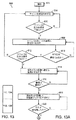
図12は、本発明による磁気強化プラズマエッチングの実例となるプロセスのフローチャート600である。そのプロセスは、図2の磁気強化プラズマ処理装置200内の様々なシステムに電圧を印加することにより、開始する(工程602)。例えば、まず、チャンバ202を特定の圧力まで真空引きする(工程604)。次いで、チャンバ202内の圧力を評価する(工程606)。一実施形態においては、次いで、チャンバに原料ガスを供給する(工程608)。   FIG. 12 is a flowchart 600 of an illustrative process for magnetically enhanced plasma etching according to the present invention. The process begins by applying voltages to various systems within the magnetically enhanced plasma processing apparatus 200 of FIG. 2 (step 602). For example, first, the chamber 202 is evacuated to a specific pressure (step 604). Next, the pressure in the chamber 202 is evaluated (step 606). In one embodiment, the source gas is then supplied to the chamber (step 608).

次いで、ガス圧を評価する(工程610)。ガス圧が適当である場合には、チャンバ202内の圧力を再び評価する(工程612)。チャンバ202内の圧力が適当である場合には、原料ガスの近傍に適当な磁場を生成する(工程614)。一実施形態において、図2の磁石系252には、少なくとも1つの永久磁石が含まれる。従って、プロセス開始前から一定の磁場が生成されている。他の実施形態において、磁石系(図示していない)には、少なくとも1つの電磁石が含まれる。従って、電磁石が作動するときにのみ磁場が生成される。   Next, the gas pressure is evaluated (step 610). If the gas pressure is appropriate, the pressure in the chamber 202 is again evaluated (step 612). If the pressure in the chamber 202 is appropriate, an appropriate magnetic field is generated in the vicinity of the source gas (step 614). In one embodiment, the magnet system 252 of FIG. 2 includes at least one permanent magnet. Therefore, a constant magnetic field is generated before the start of the process. In other embodiments, the magnet system (not shown) includes at least one electromagnet. Thus, a magnetic field is generated only when the electromagnet is activated.

磁場が適当である場合には(工程616)、原料ガスは電離して、弱電離プラズマを生成する(工程618)。一実施形態において、図2のカソード216とアノード238の間のギャップ244に比較的低い電流放電を作り出すことによって、弱電離プラズマが生成される。他の実施形態において、図7の電極452とカソード216との間に比較的低い電流放電を作り出すことによって、弱電離プラズマが生成される。さらに他の実施形態において、図11の電極452”が加熱されて、カソード216の近傍に電子を放出する。図11の実施形態において、アノード238と電極452’との間に、比較的低い電流放電が作り出される。   If the magnetic field is appropriate (step 616), the source gas is ionized to generate weakly ionized plasma (step 618). In one embodiment, a weakly ionized plasma is generated by creating a relatively low current discharge in the gap 244 between the cathode 216 and the anode 238 of FIG. In other embodiments, a weakly ionized plasma is generated by creating a relatively low current discharge between the electrode 452 and the cathode 216 of FIG. In yet another embodiment, the electrode 452 "of FIG. 11 is heated to emit electrons in the vicinity of the cathode 216. In the embodiment of FIG. 11, a relatively low current is provided between the anode 238 and the electrode 452 '. A discharge is created.

図2の実施形態において、原料ガスを導入する前に、カソード216とアノード238との間のギャップ244に電位を加えることによって、弱電離プラズマが生成される。図7に示される実施形態において、弱電離プラズマを生成する原料ガスを導入する前に、図7の電極452とカソード216との間に電位差を加えることによって、弱電離プラズマが生成される。   In the embodiment of FIG. 2, weakly ionized plasma is generated by applying a potential to the gap 244 between the cathode 216 and the anode 238 before introducing the source gas. In the embodiment shown in FIG. 7, the weakly ionized plasma is generated by applying a potential difference between the electrode 452 and the cathode 216 of FIG. 7 before introducing the source gas for generating the weakly ionized plasma.

ガスが弱電離している場合には(工程620)、基板に負のバイアスをかける(工程621)。次いで、弱電離プラズマから強電離プラズマが生成される(工程622)。一実施形態において、カソード216とアノード238との間に高電力パルスを印加することによって、強電離プラズマが生成される。上述したように、高電力パルスによって、アノード238とカソード216との間のギャップ244に強電場が生成される。その強電場によって、原子の原料ガスが段階的に電離し、強電離プラズマになる分子の原料ガスのイオン形成が促進される。一実施形態において、強電離プラズマは、図2の領域246内において実質的に均一である。その均一性により、実質的に均一な基板211のエッチングが得られる。   If the gas is weakly ionized (step 620), a negative bias is applied to the substrate (step 621). Next, a strongly ionized plasma is generated from the weakly ionized plasma (step 622). In one embodiment, a strongly ionized plasma is generated by applying a high power pulse between the cathode 216 and the anode 238. As described above, the high power pulse generates a strong electric field in the gap 244 between the anode 238 and the cathode 216. The strong electric field ionizes the atomic source gas stepwise and promotes ion formation of the molecular source gas that becomes a strongly ionized plasma. In one embodiment, the strongly ionized plasma is substantially uniform within region 246 of FIG. Due to the uniformity, substantially uniform etching of the substrate 211 is obtained.

基板211はカソード216に対して負にバイアスがかけられているために、基板211は、実質的に均一な強電離プラズマから電子を引き付ける。それにより、イオンが基板211に衝突して、基板材料のエッチングが引き起こされる。一実施形態において、強電離プラズマが形成されると(工程624)、周知のモニタリング技術を用いて、プラズマエッチングをモニタリングする(工程628)。プラズマエッチングが完了すると(工程630)、プラズマエッチング処理を終了させる(工程632)。   Since the substrate 211 is negatively biased with respect to the cathode 216, the substrate 211 attracts electrons from the substantially uniform strongly ionized plasma. Thereby, the ions collide with the substrate 211 to cause etching of the substrate material. In one embodiment, once the strongly ionized plasma is formed (step 624), the plasma etch is monitored using a well-known monitoring technique (step 628). When the plasma etching is completed (step 630), the plasma etching process is terminated (step 632).

図13は、本発明によるエッチング速度の制御の実例となるプロセスのフローチャート650である。そのプロセスは、図2の磁気強化プラズマ処理装置200内の様々なシステムに電圧を印加することにより、開始する(工程602)。例えば、まず、チャンバ202を特定の圧力まで真空引きする(工程604)。次いで、チャンバ202内の圧力を評価する(工程606)。一実施形態においては、次いで、チャンバに原料ガスを供給する(工程608)。ガス圧を評価する(工程610)。ガス圧が適当である場合には、チャンバ202内の圧力を再び評価する(工程612)。チャンバ202内の圧力が適当である場合には、原料ガスの近傍に適当な磁場を生成する(工程614)。   FIG. 13 is a flowchart 650 of an illustrative process for controlling the etch rate according to the present invention. The process begins by applying voltages to various systems within the magnetically enhanced plasma processing apparatus 200 of FIG. 2 (step 602). For example, first, the chamber 202 is evacuated to a specific pressure (step 604). Next, the pressure in the chamber 202 is evaluated (step 606). In one embodiment, the source gas is then supplied to the chamber (step 608). The gas pressure is evaluated (step 610). If the gas pressure is appropriate, the pressure in the chamber 202 is again evaluated (step 612). If the pressure in the chamber 202 is appropriate, an appropriate magnetic field is generated in the vicinity of the source gas (step 614).

磁場が適当であると仮定すると(工程616)、原料ガスは電離して、弱電離プラズマを生成する(工程618)。一実施形態において、図2のカソード216とアノード238の間に比較的低い電流放電を作り出すことによって、弱電離プラズマが生成される。   Assuming that the magnetic field is appropriate (step 616), the source gas is ionized to produce a weakly ionized plasma (step 618). In one embodiment, a weakly ionized plasma is generated by creating a relatively low current discharge between the cathode 216 and the anode 238 of FIG.

弱電離プラズマが生成された(工程620)後、基板に負のバイアスをかける(工程621)。次いで、弱電離プラズマから強電離プラズマが生成される(工程622)。一実施形態において、カソード216とアノード238との間のギャップ244に高電力パルスを印加することによって、強電離プラズマが生成される。一実施形態において、強電離プラズマは、図2の領域246内において実質的に均一である。その均一性により、実質的により均一な基板211のエッチングが得られる。基板211は、実質的に均一な強電離プラズマから電子を引き付ける。そのイオンが基板211に衝突することにより、基板材料のエッチングが引き起こされる。   After the weakly ionized plasma is generated (step 620), the substrate is negatively biased (step 621). Next, a strongly ionized plasma is generated from the weakly ionized plasma (step 622). In one embodiment, a strongly ionized plasma is generated by applying a high power pulse to the gap 244 between the cathode 216 and the anode 238. In one embodiment, the strongly ionized plasma is substantially uniform within region 246 of FIG. Due to the uniformity, a substantially more uniform etching of the substrate 211 is obtained. The substrate 211 attracts electrons from a substantially uniform strongly ionized plasma. The ions collide with the substrate 211 to cause etching of the substrate material.

一実施形態において、強電離プラズマが形成されると(工程624)、周知のモニタリング技術を用いて、エッチング速度をモニタリングする(工程652)。エッチング速度が十分でない場合(工程654)には、プラズマに供給される電力を増加させる(工程656)。一実施形態において、カソード216とアノード238との間のギャップ244に印加される高電力パルスの大きさを増すことにより、プラズマに供給される電力が増加する。一実施形態(図示していない)において、基板に衝突するイオンのイオンエネルギーを制御するために、基板にかける負のバイアス(工程621)を変更する。エッチング速度を再び評価する(工程652)。エッチング速度が十分になるまで(工程654)、このプロセスを続け、エッチングが続く(工程658)。プラズマエッチングが完了すると(工程660)、プラズマエッチング処理を終了させる(工程662)。   In one embodiment, once the strongly ionized plasma is formed (step 624), the etch rate is monitored using a well-known monitoring technique (step 652). If the etch rate is not sufficient (step 654), the power supplied to the plasma is increased (step 656). In one embodiment, increasing the magnitude of the high power pulse applied to the gap 244 between the cathode 216 and the anode 238 increases the power delivered to the plasma. In one embodiment (not shown), the negative bias applied to the substrate (step 621) is changed to control the ion energy of ions that strike the substrate. The etch rate is evaluated again (step 652). The process continues until the etch rate is sufficient (step 654) and etching continues (step 658). When the plasma etching is completed (step 660), the plasma etching process is terminated (step 662).

(等価物)
特に、特定の実施形態を参照して、本発明を示し、記載してきたが、本明細書に定められる本発明の精神および範囲から逸脱することなく、様々な形態および詳細の変更がなされ得ることは、当業者には理解されるべきである。
(Equivalent)
In particular, while the invention has been illustrated and described with reference to specific embodiments, various changes in form and detail may be made without departing from the spirit and scope of the invention as defined herein. Should be understood by those skilled in the art.

無線周波数(RF)電源を有する周知の磁気強化エッチング装置の断面図を示す。1 shows a cross-sectional view of a known magnetic enhanced etching apparatus having a radio frequency (RF) power supply. 本発明による磁気強化プラズマ処理装置の実施形態の断面図を示す。1 shows a cross-sectional view of an embodiment of a magnetically enhanced plasma processing apparatus according to the present invention. 図2の磁気強化プラズマ処理装置のアノードおよびカソードの断面図を示す。FIG. 3 shows a cross-sectional view of the anode and cathode of the magnetically enhanced plasma processing apparatus of FIG. 図2の磁気強化プラズマ処理装置においてプラズマに印加される周期的なパルスに対する印加電力を時間の関数としてグラフ表示したものを示す。FIG. 3 is a graph showing the power applied to a periodic pulse applied to plasma as a function of time in the magnetically enhanced plasma processing apparatus of FIG. 2. 図2の磁気強化プラズマ処理装置においてプラズマに加えられる周期的なパルスの印加電圧、印加電流、および、印加電力を時間の関数としてグラフ表示したものを示す。FIG. 3 shows a graphical representation of the applied voltage, applied current, and applied power of periodic pulses applied to the plasma in the magnetically enhanced plasma processing apparatus of FIG. 2 as a function of time. 本発明による、種々の電子E×Bドリフト電流に対する、カソード近傍の種々のシミュレートされた磁場分布を示す。FIG. 4 shows various simulated magnetic field distributions near the cathode for various electron E × B drift currents according to the present invention. FIG. 本発明による、種々の電子E×Bドリフト電流に対する、カソード近傍の種々のシミュレートされた磁場分布を示す。FIG. 4 shows various simulated magnetic field distributions near the cathode for various electron E × B drift currents according to the present invention. FIG. 本発明による、種々の電子E×Bドリフト電流に対する、カソード近傍の種々のシミュレートされた磁場分布を示す。FIG. 4 shows various simulated magnetic field distributions near the cathode for various electron E × B drift currents according to the present invention. FIG. 本発明による、種々の電子E×Bドリフト電流に対する、カソード近傍の種々のシミュレートされた磁場分布を示す。FIG. 4 shows various simulated magnetic field distributions near the cathode for various electron E × B drift currents according to the present invention. FIG. 本発明による磁気強化プラズマ処理装置の他の実施形態の断面図を示す。FIG. 3 shows a cross-sectional view of another embodiment of a magnetic enhanced plasma processing apparatus according to the present invention. 図7の磁気強化プラズマ処理装置においてプラズマに加えられる周期的なパルスに対して、パルス電力を時間の関数としてグラフ表示したものを示す。FIG. 8 shows a graph of pulse power as a function of time for periodic pulses applied to plasma in the magnetically enhanced plasma processing apparatus of FIG. 図9A〜図9Cは本発明によるカソードの種々の実施形態の断面図である。9A-9C are cross-sectional views of various embodiments of cathodes according to the present invention. 本発明による磁気強化プラズマ処理装置の別の実施形態を示す断面図である。It is sectional drawing which shows another embodiment of the magnetic enhancement plasma processing apparatus by this invention. 本発明による磁気強化プラズマ処理装置の別の実施形態を示す断面図である。It is sectional drawing which shows another embodiment of the magnetic enhancement plasma processing apparatus by this invention. 本発明による磁気強化プラズマ処理装置のプロセスを示すフローチャートである。It is a flowchart which shows the process of the magnetic enhancement plasma processing apparatus by this invention. 本発明による磁気強化プラズマ処理装置のプロセスを示すフローチャートである。It is a flowchart which shows the process of the magnetic enhancement plasma processing apparatus by this invention. 本発明によるエッチング速度の制御のプロセスを示すフローチャートである。3 is a flowchart showing a process of controlling an etching rate according to the present invention. 本発明によるエッチング速度の制御のプロセスを示すフローチャートである。3 is a flowchart showing a process of controlling an etching rate according to the present invention.

Claims (37)

アノードと、
該アノードに隣接して配置され、該アノードとの間にギャップを形成するカソードと、
該カソードの近傍に弱電離プラズマを生成するイオン源と、
該弱電離プラズマの近傍に磁場を生成するように配置された磁石であって、該磁場は、該カソードの近傍の該弱電離プラズマ内の電子を実質的に閉じ込める、磁石と、
該ギャップの全体に電場を作り出す電源であって、該電場は、該弱電離プラズマ内に励起原子を生成し、該カソードから二次電子を生成することにより、複数のイオンを含む強電離プラズマを作り出す、電源と、
該カソードの近傍に配置された基板にバイアス電圧を印加する電圧源であって、該バイアス電圧により、該複数のイオンの中のイオンが該基板の表面のエッチングを引き起こすように該基板の該表面に衝突する、電圧源とを備える、磁気的に強化されたプラズマ処理装置。
An anode,
A cathode disposed adjacent to the anode and forming a gap with the anode;
An ion source that generates a weakly ionized plasma in the vicinity of the cathode;
A magnet arranged to generate a magnetic field in the vicinity of the weakly ionized plasma, the magnetic field substantially confining electrons in the weakly ionized plasma in the vicinity of the cathode;
A power source that creates an electric field across the gap, the electric field generating excited atoms in the weakly ionized plasma and generating secondary electrons from the cathode, thereby generating a strongly ionized plasma containing a plurality of ions. Producing, power supply,
A voltage source for applying a bias voltage to a substrate disposed in the vicinity of the cathode, the bias voltage causing the ions in the plurality of ions to cause etching of the surface of the substrate. A magnetically enhanced plasma processing apparatus comprising a voltage source that impinges on the substrate.
前記電場が準静的な電場を含む、請求項1に記載の装置。   The apparatus of claim 1, wherein the electric field comprises a quasi-static electric field. 前記電場がパルス状の電場を含む、請求項1に記載の装置。   The apparatus of claim 1, wherein the electric field comprises a pulsed electric field. 前記電場の立上り時間を選択することにより、前記弱電離プラズマ内の前記励起原子の電離速度を増加させる、請求項1に記載の装置。   The apparatus of claim 1, wherein the ionization rate of the excited atoms in the weakly ionized plasma is increased by selecting a rise time of the electric field. 前記電場の立上り時間を選択することにより、前記基板の前記表面のエッチング速度を増加させる、請求項1に記載の装置。   The apparatus of claim 1, wherein the etching rate of the surface of the substrate is increased by selecting a rise time of the electric field. 前記弱電離プラズマが、前記アノードと前記カソードとの間に絶縁破壊状態を生み出す可能性を低減させる、請求項1に記載の装置。   The apparatus of claim 1, wherein the weakly ionized plasma reduces the likelihood of creating a breakdown condition between the anode and the cathode. 前記複数のイオンの中の前記イオンが前記基板の前記表面に衝突することにより、該基板の該表面の実質的に均一なエッチングを引き起こす、請求項1に記載の装置。   The apparatus of claim 1, wherein the ions in the plurality of ions impinge on the surface of the substrate causing a substantially uniform etch of the surface of the substrate. 前記複数のイオンの中の前記イオンが前記基板の前記表面に衝突することにより、異方的なエッチングを引き起こす、請求項1に記載の装置。   The apparatus of claim 1, wherein the ions in the plurality of ions cause anisotropic etching by impacting the surface of the substrate. 前記アノードと前記カソードとの間の体積を選択することにより、前記弱電離プラズマ内の前記励起原子および分子の電離速度を増加させる、請求項1に記載の装置。   The apparatus of claim 1, wherein the ionization rate of the excited atoms and molecules in the weakly ionized plasma is increased by selecting a volume between the anode and the cathode. 前記イオン源が、UV源と、X線源と、電子ビーム源と、イオンビーム源と、誘導結合プラズマ源と、容量結合プラズマ源と、マイクロ波プラズマ源と、電極と、DC電源と、AC電源とを含む群から選択される、請求項1に記載の装置。   The ion source includes a UV source, an X-ray source, an electron beam source, an ion beam source, an inductively coupled plasma source, a capacitively coupled plasma source, a microwave plasma source, an electrode, a DC power source, and an AC power source. The apparatus of claim 1, wherein the apparatus is selected from the group comprising a power source. 前記電源が、前記ギャップの全体に前記電場を作り出す電気パルスを生成する、請求項1に記載の装置。   The apparatus of claim 1, wherein the power source generates an electrical pulse that creates the electric field across the gap. 前記電気パルスのパルス振幅と、パルス幅とのうちの少なくとも1つを選択することにより、前記基板の前記表面のエッチング速度を増加させる、請求項11に記載の装置。   The apparatus of claim 11, wherein the etching rate of the surface of the substrate is increased by selecting at least one of a pulse amplitude and a pulse width of the electrical pulse. 前記バイアス電圧を選択することにより、前記基板の前記表面に衝突する前記複数のイオンの中の前記イオンのイオンエネルギーを制御する、請求項1に記載の装置。   The apparatus of claim 1, wherein the ion energy of the ions in the plurality of ions impinging on the surface of the substrate is controlled by selecting the bias voltage. 前記電場が、前記弱電離プラズマ内にイオンと励起原子を生成し、前記カソードから二次電子を生成し、該二次電子が、該励起原子と、励起分子と、中性原子と、中性分子とを電離することにより、前記強電離プラズマを作り出す、請求項1に記載の装置。   The electric field generates ions and excited atoms in the weakly ionized plasma, generates secondary electrons from the cathode, and the secondary electrons are the excited atoms, excited molecules, neutral atoms, neutral The apparatus of claim 1, wherein the strongly ionized plasma is created by ionizing molecules. 原料ガスを電離することにより、カソードの近傍に弱電離プラズマを生成することと、
該弱電離プラズマの近傍に磁場を生成することであって、該磁場は、該カソードの近傍の該弱電離プラズマ内の電子を実質的に閉じ込める、ことと、
該弱電離プラズマ内の原子を励起し、該カソードから二次電子を生成する該弱電離プラズマ全体に電場を印加することであって、該二次電子は該励起原子を電離することにより、複数のイオンを含む強電離プラズマを作り出す、ことと、
該カソードの近傍に配置された基板にバイアス電圧を印加することであって、該バイアス電圧により、該複数のイオンの中のイオンが該基板の表面のエッチングを引き起こすように該基板の該表面に衝突する、こととを包含する、磁気的に強化されたプラズマ処理方法。
Generating ionized plasma in the vicinity of the cathode by ionizing the source gas;
Generating a magnetic field in the vicinity of the weakly ionized plasma, the magnetic field substantially confining electrons in the weakly ionized plasma in the vicinity of the cathode;
Applying an electric field to the entire weakly ionized plasma that excites atoms in the weakly ionized plasma and generates secondary electrons from the cathode, wherein the secondary electrons ionize the excited atoms to generate a plurality of ions. Creating a strongly ionized plasma containing the ions of
Applying a bias voltage to a substrate disposed in the vicinity of the cathode, the bias voltage applying to the surface of the substrate such that ions in the plurality of ions cause etching of the surface of the substrate. A magnetically enhanced plasma processing method comprising: impinging.
前記電場を印加することが、定電力で該電場を印加することを包含する、請求項15に記載の方法。   The method of claim 15, wherein applying the electric field comprises applying the electric field at a constant power. 前記電場を印加することが、定電圧で該電場を印加することを包含する、請求項15に記載の方法。   The method of claim 15, wherein applying the electric field comprises applying the electric field at a constant voltage. 前記電場を印加することが、準静的な電場を印加することを包含する、請求項15に記載の方法。   The method of claim 15, wherein applying the electric field comprises applying a quasi-static electric field. 前記電場を印加することが、前記弱電離プラズマの全体に電気パルスを印加することを包含する、請求項15に記載の方法。   The method of claim 15, wherein applying the electric field comprises applying an electrical pulse across the weakly ionized plasma. 前記電気パルスのパルス振幅と、パルス幅とのうちの少なくとも1つを選択することにより、前記強電離プラズマの電離速度を増加させることをさらに包含する、請求項19に記載の方法。   20. The method of claim 19, further comprising increasing the ionization rate of the strongly ionized plasma by selecting at least one of a pulse amplitude and a pulse width of the electrical pulse. 前記電気パルスのパルス振幅と、パルス幅とのうちの少なくとも1つを選択することにより、前記基板の前記表面の近傍の領域において前記強電離プラズマが実質的に均一になることをさらに包含する、請求項19に記載の方法。   Further comprising making the strongly ionized plasma substantially uniform in a region near the surface of the substrate by selecting at least one of a pulse amplitude and a pulse width of the electrical pulse; The method of claim 19. 前記電気パルスのパルス振幅と、パルス幅とのうちの少なくとも1つを選択することにより、前記基板の前記表面のエッチング速度を増加させることをさらに包含する、請求項19に記載の方法。   20. The method of claim 19, further comprising increasing the etch rate of the surface of the substrate by selecting at least one of a pulse amplitude and a pulse width of the electrical pulse. 前記複数のイオンの中のイオンが、前記基板の前記表面に実質的に均一に衝突する、請求項15に記載の方法。   The method of claim 15, wherein ions in the plurality of ions substantially uniformly strike the surface of the substrate. 前記強電離プラズマが、前記基板の表面の近傍において実質的に均一である、請求項15に記載の方法。   The method of claim 15, wherein the strongly ionized plasma is substantially uniform near the surface of the substrate. 前記弱電離プラズマの前記ピークプラズマ密度が約1012cm−3未満である、請求項15に記載の方法。 The method of claim 15, wherein the peak plasma density of the weakly ionized plasma is less than about 10 12 cm −3 . 前記強電離プラズマの前記ピークプラズマ密度が約1012cm−3よりも高い、請求項15に記載の方法。 The method of claim 15, wherein the peak plasma density of the strongly ionized plasma is greater than about 10 12 cm −3 . 前記基板の前記表面の温度を制御することをさらに包含する、請求項15に記載の方法。   The method of claim 15, further comprising controlling a temperature of the surface of the substrate. 前記原料ガスを前記電離することが、電場と、UV源と、X線源と、電子ビーム源と、イオンビーム源と、誘導結合プラズマ源と、容量結合プラズマ源と、マイクロ波源と、DC電源と、AC電源とのうちの少なくとも1つに該原料ガスをさらすことを包含する、請求項15に記載の方法。   The ionization of the source gas includes an electric field, a UV source, an X-ray source, an electron beam source, an ion beam source, an inductively coupled plasma source, a capacitively coupled plasma source, a microwave source, and a DC power source. And exposing the source gas to at least one of an AC power source. 前記バイアス電圧を選択することにより、前記基板の前記表面に衝突する前記複数のイオンの中の前記イオンのイオンエネルギーを制御する、請求項15に記載の方法。   The method of claim 15, wherein the ion energy of the ions in the plurality of ions impinging on the surface of the substrate is controlled by selecting the bias voltage. 原料ガスのボリュームを電離することにより、カソードの近傍に弱電離プラズマを形成することと、
該弱電離プラズマの近傍に磁場を作り出すことであって、該磁場は、該カソードの近傍の該弱電離プラズマ内の電子を実質的に閉じ込める、ことと、
該弱電離プラズマの全体に電気パルスを印加することにより、第1の複数のイオンを含む強電離プラズマを生成することと、
原料ガスの第2のボリュームの全体に該電気パルスを印加することにより第2の複数のイオンを含む強電離プラズマを生成する間に、原料ガスの該第2のボリュームと該強電離プラズマを交換することと、
該カソードの近傍に配置された基板にバイアス電圧を印加することであって、該バイアス電圧により、該第1の複数のイオンと、該第2の複数のイオンとが該基板の表面のエッチングを引き起こすように該基板の該表面に衝突する、こととを包含する、磁気的に強化されたプラズマ処理方法。
Forming a weakly ionized plasma near the cathode by ionizing the volume of the source gas;
Creating a magnetic field in the vicinity of the weakly ionized plasma, the magnetic field substantially confining electrons in the weakly ionized plasma in the vicinity of the cathode;
Generating a strongly ionized plasma including a first plurality of ions by applying an electrical pulse across the weakly ionized plasma;
The second volume of source gas and the strongly ionized plasma are exchanged while generating a strongly ionized plasma containing a second plurality of ions by applying the electrical pulse across the second volume of source gas. To do
Applying a bias voltage to a substrate disposed in the vicinity of the cathode, wherein the first plurality of ions and the second plurality of ions cause the surface of the substrate to be etched by the bias voltage. Impacting the surface of the substrate to cause a magnetically enhanced plasma processing method.
前記強電離プラズマを交換することが、原料ガスの第2のボリュームと実質的に全ての該強電離プラズマを交換することを包含する、請求項30に記載の方法。   31. The method of claim 30, wherein exchanging the strongly ionized plasma comprises exchanging substantially all of the strongly ionized plasma with a second volume of source gas. 前記電気パルスのパルス振幅とパルス幅とのうちの少なくとも1つを選択することにより、前記強電離プラズマの電離速度を増加させることをさらに包含する、請求項30に記載の方法。   31. The method of claim 30, further comprising increasing the ionization rate of the strongly ionized plasma by selecting at least one of a pulse amplitude and a pulse width of the electrical pulse. 前記電気パルスのパルス振幅とパルス幅とのうちの少なくとも1つを選択することにより、前記基板の前記表面に隣接する領域において前記強電離プラズマが実質的に均一になることをさらに包含する、請求項30に記載の方法。   The method further comprises making the strongly ionized plasma substantially uniform in a region adjacent to the surface of the substrate by selecting at least one of a pulse amplitude and a pulse width of the electrical pulse. Item 30. The method according to Item 30. 前記電気パルスのパルス振幅とパルス幅とのうちの少なくとも1つを選択することにより、前記基板の前記表面のエッチング速度を増加させることをさらに包含する、請求項30に記載の方法。   32. The method of claim 30, further comprising increasing an etch rate of the surface of the substrate by selecting at least one of a pulse amplitude and a pulse width of the electrical pulse. 前記弱電離プラズマの全体に前記電気パルスを前記印加することにより、前記弱電離プラズマ内の原子を励起し、前記カソードから二次電子を生成し、該二次電子が該励起原子を電離することにより、前記強電離プラズマを作り出す、請求項30に記載の方法。   Applying the electric pulse to the whole weakly ionized plasma excites atoms in the weakly ionized plasma, generates secondary electrons from the cathode, and the secondary electrons ionize the excited atoms. 32. The method of claim 30, wherein the method generates the strongly ionized plasma. 原料ガスを電離することにより、カソードの近傍に弱電離プラズマを生成する手段と、
該弱電離プラズマの近傍に磁場を作り出す手段であって、該磁場は、該カソードの近傍の該弱電離プラズマ内の電子を実質的に閉じ込める、手段と、
該弱電離プラズマの全体に電場を印加することにより、該弱電離プラズマ内の原子を励起し、該カソードから二次電子を生成する手段であって、該二次電子が該励起原子を電離することにより、複数のイオンを含む強電離プラズマを作り出す、手段と、
該カソードの近傍に配置された基板にバイアス電圧を印加する手段であって、該バイアス電圧により、該複数のイオンの中のイオンが該基板の表面のエッチングを引き起こすように該基板の該表面に衝突する、手段と
を備える磁気的に強化されたプラズマ処理装置。
Means for generating weakly ionized plasma in the vicinity of the cathode by ionizing the source gas;
Means for creating a magnetic field in the vicinity of the weakly ionized plasma, the magnetic field substantially confining electrons in the weakly ionized plasma in the vicinity of the cathode;
A means for exciting atoms in the weakly ionized plasma by applying an electric field to the entire weakly ionized plasma and generating secondary electrons from the cathode, wherein the secondary electrons ionize the excited atoms. A means for creating a strongly ionized plasma containing a plurality of ions,
Means for applying a bias voltage to a substrate disposed proximate to the cathode, the bias voltage causing the ions in the plurality of ions to cause etching of the surface of the substrate to the surface of the substrate; A magnetically enhanced plasma processing apparatus comprising: means for colliding.
原料ガスのボリュームを電離することにより、カソードの近傍に弱電離プラズマを形成する手段と、
該弱電離プラズマの近傍に磁場を作り出す手段であって、該磁場は、該カソードの近傍の該弱電離プラズマ内の電子を実質的に閉じ込める、手段と、
該弱電離プラズマの全体に電気パルスを印加することにより、第1の複数のイオンを含む強電離プラズマを生成する手段と、
原料ガスの第2のボリュームの全体に該電気パルスを印加することにより第2の複数のイオンを含む強電離プラズマを生成する間に、原料ガスの該第2のボリュームと該強電離プラズマを交換する手段と、
該カソードの近傍に配置された基板にバイアス電圧を印加する手段であって、該バイアス電圧により、該第1の複数のイオンと、該第2の複数のイオンとが該基板の表面のエッチングを引き起こすように該基板の該表面に衝突する、手段とを備える、磁気的に強化されたプラズマ処理装置。
Means for forming weakly ionized plasma in the vicinity of the cathode by ionizing the volume of the source gas;
Means for creating a magnetic field in the vicinity of the weakly ionized plasma, the magnetic field substantially confining electrons in the weakly ionized plasma in the vicinity of the cathode;
Means for generating a strongly ionized plasma containing a first plurality of ions by applying an electrical pulse across the weakly ionized plasma;
The second volume of source gas and the strongly ionized plasma are exchanged while generating a strongly ionized plasma containing a second plurality of ions by applying the electrical pulse across the second volume of source gas. Means to
A means for applying a bias voltage to a substrate disposed in the vicinity of the cathode, wherein the first plurality of ions and the second plurality of ions etch the surface of the substrate by the bias voltage. A magnetically enhanced plasma processing apparatus comprising: means for impinging on the surface of the substrate to cause.
JP2004548534A 2002-10-29 2003-10-28 Plasma treatment magnetically enhanced by high power pulses Withdrawn JP2006505128A (en)

Applications Claiming Priority (2)

Application Number Priority Date Filing Date Title
US10/065,551 US6896775B2 (en) 2002-10-29 2002-10-29 High-power pulsed magnetically enhanced plasma processing
PCT/US2003/034191 WO2004040615A2 (en) 2002-10-29 2003-10-28 High-power pulsed magnetically enhanced plasma processing

Publications (1)

Publication Number Publication Date
JP2006505128A true JP2006505128A (en) 2006-02-09

Family

ID=32106072

Family Applications (1)

Application Number Title Priority Date Filing Date
JP2004548534A Withdrawn JP2006505128A (en) 2002-10-29 2003-10-28 Plasma treatment magnetically enhanced by high power pulses

Country Status (7)

Country Link
US (2) US6896775B2 (en)
EP (1) EP1556882B1 (en)
JP (1) JP2006505128A (en)
AT (1) ATE504074T1 (en)
AU (1) AU2003284194A1 (en)
DE (1) DE60336574D1 (en)
WO (1) WO2004040615A2 (en)

Cited By (4)

* Cited by examiner, † Cited by third party
Publication number Priority date Publication date Assignee Title
JP2006506521A (en) * 2002-11-14 2006-02-23 ゾンド, インコーポレイテッド High deposition rate sputtering
JP2010092835A (en) * 2008-10-03 2010-04-22 Ind Technol Res Inst Cathode and its manufacturing method as well as lithium battery utilizing the same
WO2012114941A1 (en) * 2011-02-25 2012-08-30 東レ株式会社 Magnetron electrode for plasma processing
JP2013538284A (en) * 2010-07-02 2013-10-10 アプライド マテリアルズ インコーポレイテッド Deposition apparatus and method for reducing deposition asymmetry

Families Citing this family (55)

* Cited by examiner, † Cited by third party
Publication number Priority date Publication date Assignee Title
US7541283B2 (en) * 2002-08-30 2009-06-02 Tokyo Electron Limited Plasma processing method and plasma processing apparatus
US6806651B1 (en) * 2003-04-22 2004-10-19 Zond, Inc. High-density plasma source
US9771648B2 (en) * 2004-08-13 2017-09-26 Zond, Inc. Method of ionized physical vapor deposition sputter coating high aspect-ratio structures
US7663319B2 (en) * 2004-02-22 2010-02-16 Zond, Inc. Methods and apparatus for generating strongly-ionized plasmas with ionizational instabilities
US7095179B2 (en) * 2004-02-22 2006-08-22 Zond, Inc. Methods and apparatus for generating strongly-ionized plasmas with ionizational instabilities
US9123508B2 (en) * 2004-02-22 2015-09-01 Zond, Llc Apparatus and method for sputtering hard coatings
US7084573B2 (en) * 2004-03-05 2006-08-01 Tokyo Electron Limited Magnetically enhanced capacitive plasma source for ionized physical vapor deposition
US7750575B2 (en) * 2004-04-07 2010-07-06 Zond, Inc. High density plasma source
EP1609882A1 (en) * 2004-06-24 2005-12-28 METAPLAS IONON Oberflächenveredelungstechnik GmbH Coating device and method by cathodic sputtering
US20090053833A1 (en) * 2005-01-05 2009-02-26 Ulvac, Inc. Method of Manufacturing Magnetic Multi-layered Film
US8034459B2 (en) * 2005-10-18 2011-10-11 Southwest Research Institute Erosion resistant coatings
US20090214787A1 (en) * 2005-10-18 2009-08-27 Southwest Research Institute Erosion Resistant Coatings
JP2008013829A (en) * 2006-07-07 2008-01-24 Fujitsu Ltd Method for depositing metal oxide film
KR100847007B1 (en) * 2007-05-31 2008-07-17 세메스 주식회사 Apparatus and method for treating a substrate using plasma
US7966909B2 (en) * 2007-07-25 2011-06-28 The Gillette Company Process of forming a razor blade
US8133359B2 (en) 2007-11-16 2012-03-13 Advanced Energy Industries, Inc. Methods and apparatus for sputtering deposition using direct current
US9039871B2 (en) 2007-11-16 2015-05-26 Advanced Energy Industries, Inc. Methods and apparatus for applying periodic voltage using direct current
US9520275B2 (en) 2008-03-21 2016-12-13 Tokyo Electron Limited Mono-energetic neutral beam activated chemical processing system and method of using
EP2297377B1 (en) 2008-05-30 2017-12-27 Colorado State University Research Foundation Plasma-based chemical source device and method of use thereof
EP2299922B1 (en) 2008-05-30 2016-11-09 Colorado State University Research Foundation Apparatus for generating plasma
WO2011123125A1 (en) 2010-03-31 2011-10-06 Colorado State University Research Foundation Liquid-gas interface plasma device
US8994270B2 (en) 2008-05-30 2015-03-31 Colorado State University Research Foundation System and methods for plasma application
JP5207892B2 (en) * 2008-09-11 2013-06-12 東京エレクトロン株式会社 Dry etching method
US8222822B2 (en) 2009-10-27 2012-07-17 Tyco Healthcare Group Lp Inductively-coupled plasma device
CA2794895A1 (en) 2010-03-31 2011-10-06 Colorado State University Research Foundation Liquid-gas interface plasma device
US8790791B2 (en) 2010-04-15 2014-07-29 Southwest Research Institute Oxidation resistant nanocrystalline MCrAl(Y) coatings and methods of forming such coatings
US9511572B2 (en) 2011-05-25 2016-12-06 Southwest Research Institute Nanocrystalline interlayer coating for increasing service life of thermal barrier coating on high temperature components
EP3736353A1 (en) * 2011-12-28 2020-11-11 Dai Nippon Printing Co., Ltd. Vapor deposition apparatus having pretreatment device that uses plasma
JP2014125651A (en) * 2012-12-26 2014-07-07 Kobe Steel Ltd Inline-type plasma CVD apparatus
DK2954758T5 (en) * 2013-02-06 2017-03-20 Arcelormittal Investigación Y Desarrollo Sl plasma Source
US9249500B2 (en) 2013-02-07 2016-02-02 Applied Materials, Inc. PVD RF DC open/closed loop selectable magnetron
US9532826B2 (en) 2013-03-06 2017-01-03 Covidien Lp System and method for sinus surgery
US9555145B2 (en) 2013-03-13 2017-01-31 Covidien Lp System and method for biofilm remediation
US9978568B2 (en) 2013-08-12 2018-05-22 Tokyo Electron Limited Self-sustained non-ambipolar direct current (DC) plasma at low power
CN103590011B (en) * 2013-11-08 2016-03-09 蚌埠玻璃工业设计研究院 A kind of magnetron sputtering prepares the device and method of AZO nesa coating
KR101875421B1 (en) 2014-03-06 2018-07-06 어플라이드 머티어리얼스, 인코포레이티드 Plasma abatement of compounds containing heavy atoms
US9336997B2 (en) 2014-03-17 2016-05-10 Applied Materials, Inc. RF multi-feed structure to improve plasma uniformity
US9523146B1 (en) 2015-06-17 2016-12-20 Southwest Research Institute Ti—Si—C—N piston ring coatings
US10555412B2 (en) 2018-05-10 2020-02-04 Applied Materials, Inc. Method of controlling ion energy distribution using a pulse generator with a current-return output stage
JP2020077862A (en) * 2018-11-05 2020-05-21 東京エレクトロン株式会社 Etching method and plasma processing apparatus
US11476145B2 (en) 2018-11-20 2022-10-18 Applied Materials, Inc. Automatic ESC bias compensation when using pulsed DC bias
JP7451540B2 (en) 2019-01-22 2024-03-18 アプライド マテリアルズ インコーポレイテッド Feedback loop for controlling pulsed voltage waveforms
US11508554B2 (en) 2019-01-24 2022-11-22 Applied Materials, Inc. High voltage filter assembly
US11848176B2 (en) 2020-07-31 2023-12-19 Applied Materials, Inc. Plasma processing using pulsed-voltage and radio-frequency power
US11776793B2 (en) 2020-11-13 2023-10-03 Applied Materials, Inc. Plasma source with ceramic electrode plate
US11901157B2 (en) 2020-11-16 2024-02-13 Applied Materials, Inc. Apparatus and methods for controlling ion energy distribution
US11798790B2 (en) 2020-11-16 2023-10-24 Applied Materials, Inc. Apparatus and methods for controlling ion energy distribution
US11495470B1 (en) 2021-04-16 2022-11-08 Applied Materials, Inc. Method of enhancing etching selectivity using a pulsed plasma
US11948780B2 (en) 2021-05-12 2024-04-02 Applied Materials, Inc. Automatic electrostatic chuck bias compensation during plasma processing
US11791138B2 (en) 2021-05-12 2023-10-17 Applied Materials, Inc. Automatic electrostatic chuck bias compensation during plasma processing
US11810760B2 (en) 2021-06-16 2023-11-07 Applied Materials, Inc. Apparatus and method of ion current compensation
US11569066B2 (en) 2021-06-23 2023-01-31 Applied Materials, Inc. Pulsed voltage source for plasma processing applications
US11776788B2 (en) 2021-06-28 2023-10-03 Applied Materials, Inc. Pulsed voltage boost for substrate processing
US11476090B1 (en) 2021-08-24 2022-10-18 Applied Materials, Inc. Voltage pulse time-domain multiplexing
US11694876B2 (en) 2021-12-08 2023-07-04 Applied Materials, Inc. Apparatus and method for delivering a plurality of waveform signals during plasma processing

Family Cites Families (17)

* Cited by examiner, † Cited by third party
Publication number Priority date Publication date Assignee Title
US4588490A (en) 1985-05-22 1986-05-13 International Business Machines Corporation Hollow cathode enhanced magnetron sputter device
US4983253A (en) 1988-05-27 1991-01-08 University Of Houston-University Park Magnetically enhanced RIE process and apparatus
EP0428161B1 (en) 1989-11-15 1999-02-17 Kokusai Electric Co., Ltd. Dry process system
JP2819420B2 (en) 1989-11-20 1998-10-30 東京エレクトロン株式会社 Ion source
JP3076367B2 (en) 1990-11-29 2000-08-14 キヤノン株式会社 Plasma processing equipment
US5728261A (en) 1995-05-26 1998-03-17 University Of Houston Magnetically enhanced radio frequency reactive ion etching method and apparatus
SE9704607D0 (en) 1997-12-09 1997-12-09 Chemfilt R & D Ab A method and apparatus for magnetically enhanced sputtering
JPH11354509A (en) 1998-04-07 1999-12-24 Seiko Epson Corp Method for detecting end point of plasma etching and plasma etching device
US6057244A (en) 1998-07-31 2000-05-02 Applied Materials, Inc. Method for improved sputter etch processing
US6291357B1 (en) 1999-10-06 2001-09-18 Applied Materials, Inc. Method and apparatus for etching a substrate with reduced microloading
US6270634B1 (en) 1999-10-29 2001-08-07 Applied Materials, Inc. Method for plasma etching at a high etch rate
US6451703B1 (en) 2000-03-10 2002-09-17 Applied Materials, Inc. Magnetically enhanced plasma etch process using a heavy fluorocarbon etching gas
SE519931C2 (en) 2000-06-19 2003-04-29 Chemfilt R & D Ab Device and method for pulsed, highly ionized magnetron sputtering
US6413382B1 (en) * 2000-11-03 2002-07-02 Applied Materials, Inc. Pulsed sputtering with a small rotating magnetron
US6777037B2 (en) 2001-02-21 2004-08-17 Hitachi, Ltd. Plasma processing method and apparatus
SE525231C2 (en) * 2001-06-14 2005-01-11 Chemfilt R & D Ab Method and apparatus for generating plasma
US7374636B2 (en) 2001-07-06 2008-05-20 Applied Materials, Inc. Method and apparatus for providing uniform plasma in a magnetic field enhanced plasma reactor

Cited By (9)

* Cited by examiner, † Cited by third party
Publication number Priority date Publication date Assignee Title
JP2006506521A (en) * 2002-11-14 2006-02-23 ゾンド, インコーポレイテッド High deposition rate sputtering
JP4722486B2 (en) * 2002-11-14 2011-07-13 ゾンド, インコーポレイテッド High deposition rate sputtering
JP2010092835A (en) * 2008-10-03 2010-04-22 Ind Technol Res Inst Cathode and its manufacturing method as well as lithium battery utilizing the same
US8178240B2 (en) 2008-10-03 2012-05-15 Industrial Technology Research Institute Positive electrode and method for manufacturing the same and lithium battery utilizing the same
JP2013538284A (en) * 2010-07-02 2013-10-10 アプライド マテリアルズ インコーポレイテッド Deposition apparatus and method for reducing deposition asymmetry
US9580796B2 (en) 2010-07-02 2017-02-28 Applied Materials, Inc. Deposition apparatus and methods to reduce deposition asymmetry
KR101855079B1 (en) * 2010-07-02 2018-05-09 어플라이드 머티어리얼스, 인코포레이티드 Deposition apparatus and methods to reduce deposition asymmetry
WO2012114941A1 (en) * 2011-02-25 2012-08-30 東レ株式会社 Magnetron electrode for plasma processing
JP2012188751A (en) * 2011-02-25 2012-10-04 Toray Ind Inc Magnetron electrode for plasma processing

Also Published As

Publication number Publication date
ATE504074T1 (en) 2011-04-15
DE60336574D1 (en) 2011-05-12
US6896775B2 (en) 2005-05-24
US20050167263A1 (en) 2005-08-04
US20040082187A1 (en) 2004-04-29
WO2004040615A2 (en) 2004-05-13
AU2003284194A1 (en) 2004-05-25
EP1556882B1 (en) 2011-03-30
WO2004040615A3 (en) 2004-09-23
EP1556882A2 (en) 2005-07-27

Similar Documents

Publication Publication Date Title
US6896775B2 (en) High-power pulsed magnetically enhanced plasma processing
US6853142B2 (en) Methods and apparatus for generating high-density plasma
US6903511B2 (en) Generation of uniformly-distributed plasma
US6805779B2 (en) Plasma generation using multi-step ionization
JP4722486B2 (en) High deposition rate sputtering
US7147759B2 (en) High-power pulsed magnetron sputtering
US20190368030A1 (en) Apparatus for generating high-current electrical discharges
US7446479B2 (en) High-density plasma source
US7750575B2 (en) High density plasma source

Legal Events

Date Code Title Description
A300 Application deemed to be withdrawn because no request for examination was validly filed

Free format text: JAPANESE INTERMEDIATE CODE: A300

Effective date: 20070109