JP2006343473A - Image forming apparatus - Google Patents
Image forming apparatus Download PDFInfo
- Publication number
- JP2006343473A JP2006343473A JP2005168086A JP2005168086A JP2006343473A JP 2006343473 A JP2006343473 A JP 2006343473A JP 2005168086 A JP2005168086 A JP 2005168086A JP 2005168086 A JP2005168086 A JP 2005168086A JP 2006343473 A JP2006343473 A JP 2006343473A
- Authority
- JP
- Japan
- Prior art keywords
- charging
- conductive
- charging roller
- insulating
- conductive layer
- Prior art date
- Legal status (The legal status is an assumption and is not a legal conclusion. Google has not performed a legal analysis and makes no representation as to the accuracy of the status listed.)
- Pending
Links
Images

Abstract
Description
本発明は、電子写真、静電複写機、プリンタ、ファクシミリ等の画像形成装置に用いられ、像担持体に対して所定の帯電ギャップを置いて、この像担持体を非接触帯電する帯電ローラの技術分野に関する。 The present invention is used in an image forming apparatus such as an electrophotography, an electrostatic copying machine, a printer, and a facsimile, and is a charging roller that places a predetermined charging gap with respect to an image carrier and charges the image carrier in a non-contact manner. Technical field.
従来、画像形成装置として、像担持体に対して所定の帯電ギャップを置いて、この像担持体を非接触帯電する帯電ローラが知られている(例えば、特許文献1等参照)。この特許文献1に開示の帯電ローラは、両端部に形成された凹形状の段差に、それぞれリング状の規制部材がそれらの位相を互いに不一致にして係合されている。この特許文献1に開示の帯電ローラによれば、低コストで必要な精度の帯電ギャップを得ることができる。
しかしながら、この特許文献1に開示の帯電ローラでは、両端部の凹形状の環状の段差を形成するためには、帯電ローラの基材シャフトを一旦研磨した後、更に凹形状の段差の底部を研磨する必要がある。この場合、研磨した段差の深さが一定でかつ基材シャフトの中心軸と環状の段差の底部の中心軸とが一致する(同心となる)ように加工することがきわめて難しく、段差に係合するリング状の規制部材の取付位置を、それらの位相がずれるようにして調整しても、安定した信頼性のある高精度の帯電ギャップが得られるように帯電ローラを製造することは難しいという問題がある。 However, in the charging roller disclosed in Patent Document 1, in order to form the concave annular step at both ends, the base shaft of the charging roller is first polished, and then the bottom of the concave step is further polished. There is a need to. In this case, it is extremely difficult to process the polished step so that the depth of the step is constant and the center axis of the base shaft and the center axis of the bottom of the annular step are aligned (concentric). The problem is that it is difficult to manufacture a charging roller so that a stable, reliable and highly accurate charging gap can be obtained even if the mounting positions of the ring-shaped regulating members are adjusted so that their phases are shifted. There is.
本発明は、このような事情に鑑みてなされたものであって、その目的は、像担持体の非接触帯電において、安定した信頼性のある高精度の帯電ギャップを容易に得ることのできる非接触帯電の帯電ローラを提供することである。 The present invention has been made in view of such circumstances, and an object of the present invention is to make it possible to easily obtain a stable, reliable and highly accurate charging gap in non-contact charging of an image carrier. It is to provide a charging roller with contact charging.
前述の課題を解決するために、請求項1の発明の帯電ローラは、導電性シャフト上に導電層が形成されるとともに、この導電層が像担持体に所定の帯電ギャップを置いて対向するように設けられて前記像担持体を非接触帯電する帯電ローラにおいて、前記導電性シャフトの両端部の外周面に、それぞれ環状の窪みが形成されており、前記窪みの内側の前記導電性シャフトの中央部の外周面に導電性塗装材を塗装することにより前記導電層が形成されているとともに、前記窪みの外側の前記導電性シャフトの両端部の外周面に、絶縁性弾性部材を設けることにより前記帯電ギャップを設定する絶縁層が形成されていることを特徴としている。 In order to solve the above-mentioned problems, the charging roller according to the first aspect of the present invention has a conductive layer formed on a conductive shaft, and the conductive layer faces the image carrier with a predetermined charging gap. In the charging roller provided in a non-contact manner for charging the image carrier, annular recesses are respectively formed on the outer peripheral surfaces of both ends of the conductive shaft, and the center of the conductive shaft inside the recess is formed. The conductive layer is formed by coating a conductive coating material on the outer peripheral surface of the part, and the insulating elastic member is provided on the outer peripheral surface of both ends of the conductive shaft outside the depression. An insulating layer for setting a charging gap is formed.
また、請求項2の発明は、前記絶縁性弾性部材がゴム部材からなることを特徴としている。
更に、請求項3の発明は、前記絶縁性弾性部材が熱収縮チューブからなることを特徴としている。
更に、請求項4の発明は、前記窪みの深さが前記導電層の膜厚より大きく設定されていることを特徴としている。
The invention according to
Furthermore, the invention of
Furthermore, the invention of
更に、請求項5の発明は、前記窪みの深さが前記絶縁層の膜厚より大きく設定されていることを特徴としている。
更に、請求項6の発明は、前記窪みの深さが前記導電層の膜厚と前記絶縁層の膜厚との和より大きく設定されていることを特徴としている。
更に、請求項7の発明は、前記導電性シャフトの前記窪みを形成する縁部が面取りされていることを特徴としている。
Further, the invention of
Further, the invention of
Furthermore, the invention of claim 7 is characterized in that the edge portion forming the recess of the conductive shaft is chamfered.
このように構成された本発明の帯電ローラによれば、帯電ギャップを設定する絶縁層を導電性シャフトの外周面に形成しているので、帯電ギャップを安定した信頼性のある高精度に簡単に設定することができる。しかも、導電性シャフトの窪みが直接帯電ギャップに関係しないので、窪みの加工をそれほど高精度に行う必要がなく、帯電ローラを安価に製造することができる。 According to the charging roller of the present invention configured as described above, since the insulating layer for setting the charging gap is formed on the outer peripheral surface of the conductive shaft, the charging gap can be easily and stably provided with high accuracy. Can be set. In addition, since the recess of the conductive shaft is not directly related to the charging gap, it is not necessary to process the recess with high accuracy, and the charging roller can be manufactured at low cost.
また、導電性シャフトの両端部にそれぞれ形成された環状の窪み内を導電性塗装材および絶縁性弾性部材により被覆されるようになるが、両窪みの導電性塗装材による被覆部分は、絶縁層が像担持体に当接した状態では像担持体から距離遠くなって非接触帯電の帯電ギャップを形成しなく像担持体へ放電しないので、非接触帯電に寄与しない。したがって、両窪みを導電性塗装材の塗装境界の目標として使用することができるとともに絶縁性弾性部材の固定境界の目標として使用することができ、導電性塗装材の塗装および絶縁性弾性部材の固定を容易にかつ高精度に行うことができる。 In addition, the insides of the annular recesses formed at both ends of the conductive shaft are covered with the conductive coating material and the insulating elastic member, respectively. In the state of contact with the image carrier, the distance from the image carrier becomes far, and a non-contact charging gap is not formed and the image carrier is not discharged, so that it does not contribute to non-contact charging. Therefore, both depressions can be used as targets for the coating boundary of the conductive coating material, and can also be used as targets for the fixed boundary of the insulating elastic member, so that the coating of the conductive coating material and the fixing of the insulating elastic member can be performed. Can be performed easily and with high accuracy.
更に、導電性シャフトの両端部にこれらの窪みが形成されない場合は、図2(c)に示すように両端部に絶縁性弾性部材を例えば接着剤で固定して絶縁層を形成したとき、絶縁層の内側端部の膜厚が接着剤の乾燥時の表面張力で厚くなる傾向となったり、あるいは絶縁性弾性部材として熱収縮チューブを用いて絶縁層を形成したとき、絶縁層の内側端部の膜厚が熱収縮チューブの収縮で厚くなる傾向となったりするため、ギャップ部を構成する絶縁層の一定の膜厚を形成すること、つまり一定の帯電ギャップを設定することができない。これに対して、本発明の帯電ローラによれば、導電性シャフトの両端部に窪みを形成しているので、導電性塗装材および絶縁性弾性部材がこれらの窪み内にも浸入(侵入)するので、導電性塗装材の塗装乾燥後および絶縁性弾性部材の固定後に導電層および絶縁層の端部の膜厚が厚くなる傾向が生じても、これらの傾向が両窪みで吸収されるので、帯電部を構成する導電層の膜厚およびギャップ部を構成する絶縁層の膜厚を、いずれも一定に形成することができる。したがって、より一層良好な帯電を行うことが可能となる。 Furthermore, when these recesses are not formed at both ends of the conductive shaft, insulation is formed when an insulating elastic member is formed on both ends by fixing an insulating elastic member with an adhesive, for example, as shown in FIG. When the inner end of the layer tends to become thicker due to the surface tension during drying of the adhesive, or when the insulating layer is formed using a heat shrinkable tube as an insulating elastic member, the inner end of the insulating layer Therefore, it is difficult to form a constant film thickness of the insulating layer constituting the gap portion, that is, to set a constant charging gap. On the other hand, according to the charging roller of the present invention, since the depressions are formed at both ends of the conductive shaft, the conductive coating material and the insulating elastic member enter (intrude into) these depressions. Therefore, even after the coating and drying of the conductive coating material and after fixing the insulating elastic member, even if the film thickness at the end of the conductive layer and the insulating layer tends to increase, these tendencies are absorbed in both depressions. Both the thickness of the conductive layer constituting the charging portion and the thickness of the insulating layer constituting the gap portion can be formed constant. Therefore, it becomes possible to perform even better charging.
特に、請求項4ないし7の発明によれば、両窪みの深さを、導電層の膜厚よりも大きく、あるいは各絶縁層の膜厚よりも大きく、あるいは導電層の膜厚と各絶縁層の膜厚との和よりも大きく設定しているので、したがって、これらの導電性塗装材あるいは絶縁性弾性部材が両窪みから突出するのを防止でき、両絶縁層による帯電ギャップの形成を高精度にかつ安定して形成することが可能となる。その場合、請求項6の発明によれば、両窪みをこれらが導電性塗装材および絶縁性弾性部材で重ねて被覆されたときに想定される膜厚より深くすることができる。したがって、これらの導電性塗装材および絶縁性弾性部材が両窪みから突出するのを更に効果的に防止できる。このように、両窪みの深さを、導電層よび絶縁層の端部の膜厚が厚くなる傾向を考慮して設定することで、安定した高精度の帯電ギャップをより確実に形成することができる。
In particular, according to the inventions of the fourth to seventh aspects, the depth of both depressions is larger than the thickness of the conductive layer, or larger than the thickness of each insulating layer, or the thickness of the conductive layer and each insulating layer. Therefore, it is possible to prevent these conductive coating materials or insulating elastic members from protruding from both recesses, and to form a charging gap with both insulating layers with high accuracy. And can be formed stably. In that case, according to the invention of
また、請求項7の発明によれば、両窪みを形成する導電性シャフトの縁部をいずれも面取りしているので、この縁部において、導電性シャフトの外周面から両窪み面への勾配を急変させることはない。したがって、両窪みを形成する導電性シャフトの縁部も導電性塗装材および絶縁性弾性部材によって確実に被覆することができる。これにより、両窪みを形成する導電性シャフトの縁部からの電荷のリークをより確実に防止できるとともに、その分導電層の膜厚を薄くすることが可能となる。 According to the seventh aspect of the present invention, since the edge portions of the conductive shaft forming both recesses are chamfered, the gradient from the outer peripheral surface of the conductive shaft to the both recess surfaces is formed at this edge portion. There is no sudden change. Therefore, the edge of the conductive shaft that forms both recesses can be reliably covered with the conductive coating material and the insulating elastic member. As a result, it is possible to more reliably prevent charge leakage from the edge of the conductive shaft forming both depressions, and to reduce the thickness of the conductive layer accordingly.
以下、図面を用いて本発明を実施するための最良の形態について説明する。
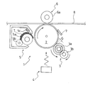
図1は、本発明にかかる非接触帯電ローラの実施の形態の一例を備えた画像形成装置の一例を模式的にかつ部分的に示す図である。
The best mode for carrying out the present invention will be described below with reference to the drawings.
FIG. 1 is a diagram schematically and partially showing an example of an image forming apparatus provided with an example of an embodiment of a non-contact charging roller according to the present invention.
図1に示すように、この例の画像形成装置1は静電潜像およびトナー像が形成される像担持体である感光体2を備えているとともに、この感光体2の周囲に感光体2の回転方向(図1では、時計回り)上流側から、順次、帯電装置3、光書込み装置4、現像装置5、転写装置6、およびクリーニング装置7を備えている。
As shown in FIG. 1, the image forming apparatus 1 of this example includes a
帯電装置3は、本実施の形態の非接触の帯電ローラ3aおよび例えばローラ等からなるクリーニング部材3bを有している。そして、帯電ローラ3aにより感光体2を一様帯電するとともに、クリーニング部材3bにより帯電ローラ3aをクリーニングして帯電ローラ3aに付着するトナーやごみ等の異物を除去する。
The
図2(a)に示すように、非接触の帯電ローラ3aは芯金3cを備えており、この芯金3cは導電性を有する、例えば金属シャフト等からなる導電性シャフトとして構成されている。この導電性シャフトとしては、例えばSUM22の表面にNiめっきを施したものを用いることができる。
As shown in FIG. 2A, the
芯金3cの両端部の外周面には、それぞれ環状の窪み3d,3eが形成されている。これらの窪み3d,3eの内側の芯金3cの中央部3fの外周面には、導電性塗装材を例えばスプレー塗装で塗装することにより導電層3gが形成されている。その場合、導電性塗装材は両窪み3d,3e内にも浸入して芯金3cの両窪み3d,3e形成部分も部分的に被覆するようになる。この導電層3gは、感光体2に対して所定の帯電ギャップGで非接触帯電を行う帯電部を構成している。
On the outer peripheral surface of both ends of the
また、窪み3d,3eの外側の芯金3cの両端部3h,3iの外周面には、それぞれ、絶縁性弾性部材を固定することにより絶縁層3j,3kが形成されている。その場合、絶縁性弾性部材は両窪み3d,3e内にも侵入して芯金3cの両窪み3d,3e形成部分も部分的に被覆するととともに、芯金3cの両端面も被覆するようになる。これらの絶縁層3j,3kの外径は互いに等しく設定されている。両絶縁層3j,3kの膜厚は導電層3gの膜厚より大きく設定されている。したがって、これらの絶縁層3j,3kは、感光体2に当接して導電層3gと感光体2との間に、これらの膜厚の差に基づく所定の帯電ギャップGを設定するギャップ部を構成している。このように、ギャップ部材である絶縁性弾性部材からなる絶縁層3j,3kが芯金3cの外周面(表面)に形成されている。
Insulating
そして、図2(b)に示すように窪み3dの深さt1は、導電層3gの膜厚t2と絶縁層3jの膜厚t3との和よりも大きく設定されている[t1 > (t2 + t3 )]。したがって、窪み3dの深さt1は導電層3gの膜厚t2および絶縁層3jの膜厚t3のいずれよりも大きく設定される(t1 > t2、t1 > t3、t3 > t2)。
また、芯金3Cの窪み3dを形成する縁部がいずれも面取り(Cカット)cを施されている。更に、芯金3cの端部3hの縁部も面取り(Cカット)cを施されている。これらの面取りcは通常R部と称され、縁部が湾曲面でカットされて丸くされているものである。もちろん、面取りcは縁部を平らな傾斜面でカットすることで形成することもできる、
Then, the depth t 1 of the 3d recess as shown in FIG. 2 (b), it is set larger than the sum of the thickness t 2 of the
In addition, the edges forming the
なお、図2(b)には一方の端部3h側の窪み3dおよび絶縁層3jについて示されているが、他方の端部3i側の窪み3eおよび絶縁層3kについてもそれぞれ端部3h側の窪み3dおよび絶縁層3jと同じに形成されている。
芯金3cに対する導電層3gおよび両絶縁層3j,3kの各形成はそれらの順序に関係なく、導電層3g先に形成した後に両絶縁層3j,3kを形成してもよいし、その逆でもよい。
2B shows the
Regardless of the order of forming the
光書込み装置4は、例えばレーザ光等により感光体2に静電潜像を書き込む。また、現像装置5は、現像ローラ5a、トナー供給ローラ5bおよびトナー層厚規制部材5cを有している。そして、トナー供給ローラ5bによって現像ローラ5a上に現像剤であるトナーTが供給されるとともに、この現像ローラ5a上のトナーTがトナー層厚規制部材5cによりその厚みを規制されて感光体2の方へ搬送され、搬送されたトナーTで感光体2上の静電潜像が現像されて感光体2上にトナー像が形成される。
The
転写装置6は転写ローラ6aを有し、この転写ローラ6aにより感光体2上にトナー像が転写紙や中間転写媒体等の転写媒体8に転写される。そして、トナー像が転写媒体8である転写紙に転写された場合には、転写紙上のトナー像が図示しない定着装置によって定着され、転写紙に画像が形成され、また、トナー像が転写媒体8である中間転写媒体に転写された場合には、中間転写媒体上のトナー像が更に転写紙に転写された後、転写紙上のトナー像が図示しない定着装置によって定着され、転写紙に画像が形成される。
The
クリーニング装置7は例えばクリーニングブレード等のクリーニング部材7aを有し、このクリーニング部材7aにより感光体2がクリーニングされて、感光体2上の転写残りトナーが除去されかつ回収される。
The cleaning device 7 includes a cleaning member 7a such as a cleaning blade. The
このように構成されたこの例の非接触の帯電ローラ3aによれば、ギャップ部材である絶縁性弾性部材からなる絶縁層3j,3kを芯金3cの外周面に形成しているので、帯電ギャップGを安定した高精度に簡単に設定することができる。しかも、芯金3cの窪み3d,3eが直接帯電ギャップGに関係しないので、窪みの加工をそれほど高精度に行う必要がなく、帯電ローラ3aを安価に製造することができる。
According to the
また、芯金3cの両端部3h,3iにそれぞれ形成された環状の窪み3d,3e内を導電性塗装材および絶縁性弾性部材により被覆されるようになるが、両窪み3d,3eの導電性塗装材による被覆部分は、絶縁層3j,3kが感光体2に当接した状態では感光体2から距離遠くなって非接触帯電の帯電ギャップGを形成しなく感光体2へ放電しないので、非接触帯電に寄与しない。したがって、両窪み3d,3eを導電性塗装材の塗装境界の目標として使用することができるとともに絶縁性弾性部材の固定境界の目標として使用することができ、導電性塗装材の塗装および絶縁性弾性部材の固定を容易にかつ高精度に行うことができる。
The
更に、芯金3cの両端部3h,3iにこれらの窪み3d,3eが形成されない場合は、図2(c)に示すように両端部3h,3iに絶縁性弾性部材を、例えば接着剤で固定して絶縁層3j,3kを形成したとき、絶縁層3j,3kの内側端部3m,3nの膜厚が接着剤の乾燥時の表面張力で厚くなる傾向となったり、あるいは絶縁性弾性部材として熱収縮チューブを用いて絶縁層3j,3kを形成したとき、絶縁層3j,3kの内側端部3m,3nの膜厚が熱収縮チューブの収縮で厚くなる傾向となったりするため、ギャップ部を構成する絶縁層3j,3kの一定の膜厚を形成すること、つまり一定の帯電ギャップGを設定することができない。
Further, when these
また、導電層3gの両端部の膜厚が導電性塗装材の塗装後の乾燥時の表面張力で厚くなる傾向となるため、導電層3gの一定の膜厚を形成すること、つまり一定の帯電ギャップGを設定することができない。これに対して、この例の帯電ローラ3aによれば、芯金3cの両端部3h,3iに窪み3d,3eを形成しているので、導電性塗装材および絶縁性弾性部材がこれらの窪み3d,3e内にも浸入(侵入)するので、導電性塗装材の塗装かつ乾燥後および絶縁性弾性部材の固定後に、導電層3gおよび絶縁層3j,3kの端部の膜厚が厚くなる傾向が生じても、この傾向が両窪み3d,3eで吸収されるので、帯電部を構成する導電層3gの膜厚およびギャップ部を構成する絶縁層3j,3kの膜厚を、いずれも一定に形成することができる。したがって、より一層良好な帯電を行うことが可能となる。
Further, since the film thickness at both ends of the
更に、両窪み3d,3eを形成する芯金3cの縁部をいずれも面取りcしているので、この縁部において、芯金3cの外周面から両窪み3d,3e面への勾配を急変させることはない。したがって、両窪み3d,3eを形成する芯金3cの縁部も導電性塗装材および絶縁性弾性部材によって確実に被覆することができる。これにより、両窪み3d,3eを形成する芯金3cの縁部からの電荷のリークをより確実に防止できるとともに、その分導電層3gの膜厚を薄くすることが可能となる。
Further, since the edges of the cored
更に、両窪み3d,3eの深さt1を、導電層3gの膜厚t2と各絶縁層3j,3kの膜厚t3との和よりも大きく設定しているので、両窪み3d,3eをこれらが導電性塗装材および絶縁性弾性部材で重ねて被覆されたときに想定される膜厚より深くすることができる。したがって、これらの導電性塗装材および絶縁性弾性部材が両窪み3d,3eから突出するのを防止でき、両絶縁層3j,3kによる帯電ギャップGの形成を高精度にかつ安定して形成することが可能となる。このように、両窪み3d,3eの深さを、導電層3gおよび絶縁層3j,3kの端部の膜厚が厚くなる傾向を考慮して設定することで、安定した高精度の帯電ギャップGをより確実に形成することができる。
Furthermore, both
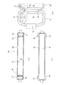
図3は本発明の帯電ローラの実施の形態の他の例およびその比較例を示し、(a)は軸方向に沿う断面図、(b)は(a)における部分拡大断面図、(c)は比較例を示す軸方向に沿う断面図である。なお、前述の図2(a)ないし(c)に示す例と同じ構成要素には同じ符号を付すことでその詳細な説明は省略する。 FIG. 3 shows another example of the embodiment of the charging roller of the present invention and a comparative example thereof, (a) is a sectional view along the axial direction, (b) is a partially enlarged sectional view in (a), (c). These are sectional drawings in alignment with the axial direction which shows a comparative example. The same components as those in the example shown in FIGS. 2A to 2C are denoted by the same reference numerals, and detailed description thereof is omitted.
前述の図2(a)および(b)に示す例の帯電ローラ3aでは、両窪み3d,3eの内側における芯金3cの中央部3fの外周面に導電層3gを形成するとともに、両窪み3d,3eの外側における芯金3cの両端部3h,3iの外周面に絶縁層3j,3kを形成しているが、図3(a)および(b)に示すように、この例の帯電ローラ3aでは、導電層3gが芯金3cの中央部3fの外周面、両窪み3d,3eにおける芯金3cの外周面、および芯金3cの両端部3h,3iの外周面のいずれにも形成されているとともに、芯金3cの両端部3h,3iの外周面に形成された導電層3の上(外周面)に絶縁層3j,3kがそれぞれ形成されている。その場合、両窪み3d,3eにおける芯金3cの外周面に形成された導電層3gには、それぞれ両窪み3d,3eに対応して窪み3o,3pが形成されており、絶縁性弾性部材はこれらの窪み3o,3p内にも部分的に侵入して設けられている。
In the charging
この例の帯電ローラ3aの場合は、芯金3cの外周面に導電性塗装材を先に塗装した後に絶縁性弾性部材を固定するようになる。また、この例の帯電ローラ3aにおいても、図3(c)に示すように芯金3cの両端部に窪み3d,3eが設けられないと、前述と同様に絶縁層3j,3kの内側端部3m,3nの膜厚が絶縁性弾性部材の固定後に厚くなる傾向となるため、ギャップ部を構成する絶縁層3j,3kの一定の膜厚を形成することができなくなる。
この例の帯電ローラ3aの他の構成および作用効果は、前述の図2(a)および(b)に示す例のそれらと同じである。
In the case of the charging
Other configurations and operational effects of the charging
次に、本発明の非接触の帯電ローラの実施例および比較例について説明する。本発明に属する実施例および本発明に属さない比較例の各帯電ローラを作製し、これらの帯電ローラ3aを用いて、本発明の帯電ローラが前述の作用効果を得ることができることを実証するために行った実験について説明する。
実験で用いた実施例および比較例の帯電ローラおよび実験結果を表1に示す。
Next, examples and comparative examples of the non-contact charging roller of the present invention will be described. In order to verify that the charging roller of the present invention can obtain the above-described effects by using the charging
Table 1 shows the charging rollers and experimental results of Examples and Comparative Examples used in the experiment.
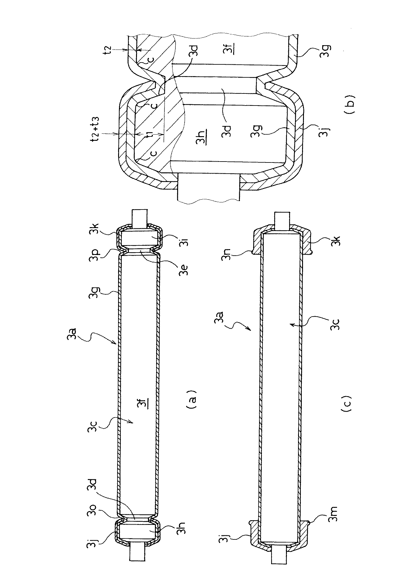
表1において、No. 1〜15は、図2(a),(b)および図3(a),(b)に示すように芯金3cの両端部に窪み3d,3eが形成された実施例の帯電ローラであり、No. 16〜18は、図2(c)および図3(c)に示すように芯金3cの両端部に窪み3d,3eが形成されない比較例の帯電ローラである。各実施例のうち、No. 1〜9は窪み3d,3eの縁部にCカットが施されたものであり、No. 10〜15は窪み3d,3eの縁部にCカットが施されずストレートに形成されたものである。
In Table 1, Nos. 1 to 15 are examples in which
各例の帯電ローラの芯金のシャフト径(芯金3cの導電層3gが形成される部分の直径)は、いずれもφ8mmである。この芯金3cは、SUM22の表面にNiめっきを施したものを用いた。芯金に形成した窪みは、No. 1、4、7、10,11、14、および15の帯電ローラについては100μmに設定し、また、No. 2、5、8、および12の帯電ローラについては125μmに設定し、更に、No. 3、6、9、および13の帯電ローラについては150μmに設定した。
また、導電性塗装材および絶縁性弾性部材は、表2に示すものを用いた。
The shaft diameter of the cored bar (the diameter of the portion where the
The conductive coating material and the insulating elastic member shown in Table 2 were used.
表2に示すように、導電性塗装材は、導電性SnO2を19重量%(wt%)、ポリウレタン(PU)樹脂を18wt%、イオン導電材3wt%、および水60wt%を混合した塗装液である。導電性SnO2は、表3に示す株式会社ジェムコ製のものがあり、それらの詳細は株式会社ジェムコのホームページ(http://www.jemco-mmc.co.jp/corporate/index.html)に掲載されている。 As shown in Table 2, the conductive coating material is a coating liquid in which conductive SnO 2 is mixed by 19 wt% (wt%), polyurethane (PU) resin is 18 wt%, ionic conductive material is 3 wt%, and water is 60 wt%. It is. Conductive SnO 2 is available from Gemco Co., Ltd. shown in Table 3. Details of those are available on the Gemco website (http://www.jemco-mmc.co.jp/corporate/index.html). It is posted.
本実施例および本比較例で用いた導電性SnO2は、株式会社ジェムコの商品名「T−1」であり、この「T−1」はスズ−アンチモン系酸化物である。もちろん、本発明では、他の導電性SnO2を用いることができる。
また、イオン導電材は導電性塗装材に導電性を持たせるためのものであり、本実施例および本比較例で用いたイオン導電材は「YYP−12」(丸菱油化工業株式会社製)である。
The conductive SnO 2 used in this example and this comparative example is trade name “T-1” of Gemco Co., Ltd., and “T-1” is a tin-antimony oxide. Of course, other conductive SnO 2 can be used in the present invention.
In addition, the ion conductive material is for imparting conductivity to the conductive coating material, and the ion conductive material used in this example and this comparative example is “YP-12” (manufactured by Maruhishi Oil Chemical Co., Ltd.). ).
更に、絶縁層3j,3kを構成するギャップ部材である絶縁性弾性部材は、ギャップ部材(1)がPET製熱収縮チューブであり、ギャップ部材(2)がポリウレタン(PU)樹脂製の弾性ゴムである。その場合、PET製熱収縮チューブは固定前の膜厚が50μmであり、固定後の膜厚が20μmである(すなわち、帯電ギャップGは20μmである)。
Furthermore, the insulating elastic member which is a gap member constituting the insulating
そして、各例の帯電ローラの製造方法は、No. 1ないし3、10ないし13、および16の帯電ローラについては、まず絶縁性弾性部材を芯金の両端部に固定して絶縁層を形成した後、次に導電性塗装材を芯金の中央部にスプレー塗装により塗装して導電層を形成する製造方法(1)で製造した。また、No. 4ないし6、14、および17の帯電ローラについては、まず導電性塗装材を芯金の中央部にスプレー塗装により塗装して導電層を形成した後、次に絶縁性弾性部材を芯金の両端部に固定して絶縁層を形成する製造方法(2)で製造した。この製造方法(2)では、絶縁層と芯金との間には導電層は存在しない。更に、No. 7ないし9、15、および18の帯電ローラについては、まず導電性塗装材を芯金の中央部、窪み、および両端部にスプレー塗装により塗装して導電層を形成した後、次に絶縁性弾性部材を芯金の両端部の導電層の上に固定して絶縁層を形成する製造方法(3)で製造した。この製造方法(3)では、絶縁層と芯金との間には導電層は存在する。なお、表1では製造方法を○1ないし○3で記載しているが、これらはそれぞれ前述の製造方法(1)ないし(3)である。また、表1および表2ではギャップ部材を○1および○2で記載しているが、これらはそれぞれ前述のギャップ部材(1)および(2)である。 In the charging roller manufacturing method of each example, for the charging rollers of No. 1 to 3, 10 to 13, and 16, first, an insulating elastic member was fixed to both ends of the cored bar to form an insulating layer. Thereafter, the conductive coating material was manufactured by the manufacturing method (1) in which the conductive layer was formed by spray coating the central portion of the core metal by spray coating. For the charging rollers of Nos. 4 to 6, 14, and 17, a conductive coating material is first applied to the central portion of the core metal by spray coating to form a conductive layer, and then an insulating elastic member is applied. Manufactured by a production method (2) in which an insulating layer is formed by fixing to both ends of the cored bar. In this manufacturing method (2), there is no conductive layer between the insulating layer and the cored bar. Further, for the charging rollers of Nos. 7 to 9, 15, and 18, first, a conductive coating material is first applied by spray coating to the central portion, the depression, and both ends of the core metal to form a conductive layer. Further, the insulating elastic member was fixed on the conductive layers on both ends of the cored bar, and the insulating layer was formed by the manufacturing method (3). In this manufacturing method (3), a conductive layer exists between the insulating layer and the cored bar. In Table 1, the production methods are indicated by ○ 1 to ○ 3, which are the above-described production methods (1) to (3), respectively. In Tables 1 and 2, the gap members are indicated by ◯ 1 and ◯ 2, which are the aforementioned gap members (1) and (2), respectively.
感光体はセイコーエプソン株式会社製のLP−9000Cと同じ材料のものを用いて感光層の膜厚をいずれも23μmに設定し、感光体の直径は、φ24mmに設定し、感光体の周速は250mm/secに設定した。 The photoconductor is the same material as LP-9000C manufactured by Seiko Epson Corporation. The photoconductor layer thickness is set to 23 μm, the photoconductor diameter is set to 24 mm, and the peripheral speed of the photoconductor is It was set to 250 mm / sec.
画像形成装置の実験装置は前述のLP−9000Cと同じ構成となるように構成した。帯電ローラ3aの印加電圧VC(V)は、直流電圧DC成分VDC(V)に交流電圧AC成分VAC(V)を重畳して、
VC = VDC + VAC = −650 + (1/2)VPP・sin2πft
(ここで、VPP=1800V、f=1.5kHzであり、VACはsin波である。)
に設定した。実験は温度23℃で湿度50%の室内環境で、A4の普通紙にハーフトーン25%のベタ印字を行い、10k(10000)枚のモノクロ耐久試験を行った。
The experimental apparatus of the image forming apparatus was configured to have the same configuration as the LP-9000C described above. The applied voltage V C (V) of the charging
V C = V DC + V AC = −650 + (1/2) V PP · sin2πft
(Here, V PP = 1800 V, f = 1.5 kHz, and V AC is a sin wave.)
Set to. In the experiment, in a room environment at a temperature of 23 ° C. and a humidity of 50%, a solid printing of 25% halftone on A4 plain paper was performed, and a monochrome durability test of 10k (10000) sheets was performed.
目視で所望の(実用に供し得る)印字濃度の画像が得られて帯電が良好であると判断したものを○で表し、リークにより感光体に孔が開いたものおよび絶縁性弾性部材が外れて(帯電ローラの軸方向に位置ずれして)帯電不良を生じたものを不良であると判断し、×で表した。 When the image of the desired print density (which can be used practically) is obtained visually and is judged to have good charging, it is indicated by ◯, and the photosensitive member is perforated and the insulating elastic member is detached. Those in which charging failure occurred due to positional displacement in the axial direction of the charging roller were determined to be defective and represented by x.
No. 1〜9、および11〜15の各実施例の帯電ローラでは、いずれも○で良好な帯電が得られた。なお、No. 10の実施例の帯電ローラでは、導電層の膜厚が薄すぎたため、窪みの縁部に導電層が形成されず、窪みの縁部における芯金が剥き出しになってしまい、印字開始直後から電荷のリークが生じてしまい、不良の結果となった。これは、本発明の芯金に窪みを設けたことによるものではなく、導電層の膜厚が薄すぎたことに起因するものである。したがって、導電層の膜厚は所定の厚みに設定する必要があるが、この膜厚は必要に応じて適宜設定すればよい。また、電荷のリークを防止するためには、窪みの縁部に面取り(Cカット)を施して窪みの縁部に導電層を確実に形成することが好ましいことが分かった。 In each of the charging rollers of Examples Nos. 1 to 9 and 11 to 15, good charging was obtained with ◯. In the charging roller of Example No. 10, since the conductive layer was too thin, the conductive layer was not formed at the edge of the recess, and the cored bar at the edge of the recess was exposed, and printing was not possible. A charge leak occurred immediately after the start, resulting in a failure. This is not due to the depression in the cored bar of the present invention, but is due to the film thickness of the conductive layer being too thin. Therefore, the film thickness of the conductive layer needs to be set to a predetermined thickness, but this film thickness may be appropriately set as necessary. Further, it has been found that in order to prevent charge leakage, it is preferable to chamfer (C cut) the edge of the recess to reliably form the conductive layer on the edge of the recess.
更に、窪みが形成されないNo. 16〜18の比較例の帯電ローラでは、いずれも、10k枚までの印字において、絶縁層を構成する絶縁性弾性部材が正規の位置から帯電ローラの軸方向に外れて帯電不良を生じてしまい、不良の結果となった。
この実験により、帯電ローラ3による感光体2の非接触帯電において、帯電ローラ3の両端部に窪みを設けることで、前述の本発明の効果が得られることが実証された。
Further, in each of the charging rollers of comparative examples No. 16 to 18 where no depression is formed, the insulating elastic member constituting the insulating layer is displaced from the normal position in the axial direction of the charging roller in printing up to 10k sheets. As a result, a charging failure occurred, resulting in a failure.
From this experiment, it was proved that the above-described effect of the present invention can be obtained by providing depressions at both ends of the charging
本発明の帯電ローラは、電子写真、静電複写機、プリンタ、ファクシミリ等の画像形成装置に用いられ、感光体に対して所定の帯電ギャップを置いて、この感光体を非接触帯電する帯電ローラであって、金属シャフトの上に帯電部である導電層が形成された帯電ローラに好適に利用することができる。 The charging roller of the present invention is used in an image forming apparatus such as an electrophotography, an electrostatic copying machine, a printer, and a facsimile, and a charging roller that places a predetermined charging gap on the photosensitive member and charges the photosensitive member in a non-contact manner. And it can utilize suitably for the charging roller in which the conductive layer which is a charging part was formed on the metal shaft.
1…画像形成装置、2…感光体、3…非接触帯電装置、3a…帯電ローラ、3c…芯金(金属シャフト)、3d,3e…窪み、3g…導電層、3j,3k…絶縁層、c…面取り(Cカット) DESCRIPTION OF SYMBOLS 1 ... Image forming apparatus, 2 ... Photoconductor, 3 ... Non-contact charging device, 3a ... Charging roller, 3c ... Core metal (metal shaft), 3d, 3e ... Depression, 3g ... Conductive layer, 3j, 3k ... Insulating layer, c ... Chamfer (C cut)
Claims (7)
前記導電性シャフトの両端部の外周面に、それぞれ環状の窪みが形成されており、
前記窪みの内側の前記導電性シャフトの中央部の外周面に導電性塗装材を塗装することにより前記導電層が形成されているとともに、前記窪みの外側の前記導電性シャフトの両端部の外周面に、絶縁性弾性部材を設けることにより前記帯電ギャップを設定する絶縁層が形成されていることを特徴とする帯電ローラ。 In a charging roller in which a conductive layer is formed on a conductive shaft, and the conductive layer is provided to face the image carrier with a predetermined charging gap to charge the image carrier in a non-contact manner.
An annular depression is formed on each of the outer peripheral surfaces of both ends of the conductive shaft,
The conductive layer is formed by coating a conductive coating material on the outer peripheral surface of the central portion of the conductive shaft inside the recess, and the outer peripheral surfaces of both ends of the conductive shaft outside the recess. In addition, an insulating layer that sets the charging gap is formed by providing an insulating elastic member.
Priority Applications (3)
| Application Number | Priority Date | Filing Date | Title |
|---|---|---|---|
| JP2005168086A JP2006343473A (en) | 2005-06-08 | 2005-06-08 | Image forming apparatus |
| US11/449,473 US7539443B2 (en) | 2005-06-08 | 2006-06-08 | Charging roller and image forming apparatus |
| US12/426,025 US20090208239A1 (en) | 2005-06-08 | 2009-04-17 | Charging Roller and Image Forming Apparatus |
Applications Claiming Priority (1)
| Application Number | Priority Date | Filing Date | Title |
|---|---|---|---|
| JP2005168086A JP2006343473A (en) | 2005-06-08 | 2005-06-08 | Image forming apparatus |
Publications (1)
| Publication Number | Publication Date |
|---|---|
| JP2006343473A true JP2006343473A (en) | 2006-12-21 |
Family
ID=37640493
Family Applications (1)
| Application Number | Title | Priority Date | Filing Date |
|---|---|---|---|
| JP2005168086A Pending JP2006343473A (en) | 2005-06-08 | 2005-06-08 | Image forming apparatus |
Country Status (1)
| Country | Link |
|---|---|
| JP (1) | JP2006343473A (en) |
Cited By (5)
| Publication number | Priority date | Publication date | Assignee | Title |
|---|---|---|---|---|
| US9840715B1 (en) | 2011-09-13 | 2017-12-12 | Monsanto Technology Llc | Methods and compositions for delaying senescence and improving disease tolerance and yield in plants |
| US9920326B1 (en) | 2011-09-14 | 2018-03-20 | Monsanto Technology Llc | Methods and compositions for increasing invertase activity in plants |
| US10000767B2 (en) | 2013-01-28 | 2018-06-19 | Monsanto Technology Llc | Methods and compositions for plant pest control |
| US10077451B2 (en) | 2012-10-18 | 2018-09-18 | Monsanto Technology Llc | Methods and compositions for plant pest control |
| US10435701B2 (en) | 2013-03-14 | 2019-10-08 | Monsanto Technology Llc | Methods and compositions for plant pest control |
-
2005
- 2005-06-08 JP JP2005168086A patent/JP2006343473A/en active Pending
Cited By (8)
| Publication number | Priority date | Publication date | Assignee | Title |
|---|---|---|---|---|
| US9840715B1 (en) | 2011-09-13 | 2017-12-12 | Monsanto Technology Llc | Methods and compositions for delaying senescence and improving disease tolerance and yield in plants |
| US10435702B2 (en) | 2011-09-13 | 2019-10-08 | Monsanto Technology Llc | Methods and compositions for delaying senescence and improving disease tolerance and yield in plants |
| US9920326B1 (en) | 2011-09-14 | 2018-03-20 | Monsanto Technology Llc | Methods and compositions for increasing invertase activity in plants |
| US10428338B2 (en) | 2011-09-14 | 2019-10-01 | Monsanto Technology Llc | Methods and compositions for increasing invertase activity in plants |
| US10077451B2 (en) | 2012-10-18 | 2018-09-18 | Monsanto Technology Llc | Methods and compositions for plant pest control |
| US10844398B2 (en) | 2012-10-18 | 2020-11-24 | Monsanto Technology Llc | Methods and compositions for plant pest control |
| US10000767B2 (en) | 2013-01-28 | 2018-06-19 | Monsanto Technology Llc | Methods and compositions for plant pest control |
| US10435701B2 (en) | 2013-03-14 | 2019-10-08 | Monsanto Technology Llc | Methods and compositions for plant pest control |
Similar Documents
| Publication | Publication Date | Title |
|---|---|---|
| JP4692746B2 (en) | Charging roller, charging roller manufacturing method, and image forming apparatus provided with charging roller | |
| JP2006343473A (en) | Image forming apparatus | |
| JP2011022577A (en) | Charging device, image forming apparatus, and method of maintaining gap between charging roller and photoconductive drum | |
| JP3729123B2 (en) | Charging device and image forming apparatus using the same | |
| JP2006343474A (en) | Image forming apparatus | |
| JP6623582B2 (en) | Conductive roll, transfer unit, and image forming apparatus | |
| JP2008015255A (en) | Charging member, process cartridge and image forming apparatus | |
| JP2006343472A (en) | Image forming apparatus | |
| JP6821425B2 (en) | Image forming device | |
| JP2008242141A (en) | Charge roller and image forming apparatus equipped with charge roller | |
| JP2008281865A (en) | Conductive member, process cartridge having same, and image forming apparatus having process cartridge | |
| JP2006201228A (en) | Image forming apparatus | |
| JP4706829B2 (en) | Image forming apparatus | |
| JP2003316130A (en) | Charging means, image forming unit using same, and image forming device | |
| JP2008026597A (en) | Image forming apparatus | |
| JP6938145B2 (en) | Image forming device | |
| JP2006145940A (en) | Image forming apparatus equipped with contact charging means and process cartridge to be equipped to image forming apparatus | |
| JP2006072066A (en) | Image forming apparatus | |
| JP2016057395A (en) | Charging device and image formation device | |
| JP2007041138A (en) | Image forming apparatus | |
| JP5047647B2 (en) | Method for manufacturing conductive member | |
| JP2008040078A (en) | Electrifying roller and image forming apparatus equipped therewith | |
| JP2007041136A (en) | Image forming apparatus | |
| JP2009086441A (en) | Charging device, process cartridge and image forming apparatus | |
| JP2006072065A (en) | Roller for proximate electrification and image forming apparatus using the same |