JP2006313913A - Organic thin film transistor indication plate and its manufacturing method - Google Patents
Organic thin film transistor indication plate and its manufacturing method Download PDFInfo
- Publication number
- JP2006313913A JP2006313913A JP2006129039A JP2006129039A JP2006313913A JP 2006313913 A JP2006313913 A JP 2006313913A JP 2006129039 A JP2006129039 A JP 2006129039A JP 2006129039 A JP2006129039 A JP 2006129039A JP 2006313913 A JP2006313913 A JP 2006313913A
- Authority
- JP
- Japan
- Prior art keywords
- thin film
- film transistor
- transistor array
- array panel
- organic
- Prior art date
- Legal status (The legal status is an assumption and is not a legal conclusion. Google has not performed a legal analysis and makes no representation as to the accuracy of the status listed.)
- Pending
Links
Images


Classifications
-
- H—ELECTRICITY
- H10—SEMICONDUCTOR DEVICES; ELECTRIC SOLID-STATE DEVICES NOT OTHERWISE PROVIDED FOR
- H10K—ORGANIC ELECTRIC SOLID-STATE DEVICES
- H10K30/00—Organic devices sensitive to infrared radiation, light, electromagnetic radiation of shorter wavelength or corpuscular radiation
- H10K30/60—Organic devices sensitive to infrared radiation, light, electromagnetic radiation of shorter wavelength or corpuscular radiation in which radiation controls flow of current through the devices, e.g. photoresistors
- H10K30/65—Light-sensitive field-effect devices, e.g. phototransistors
-
- A—HUMAN NECESSITIES
- A63—SPORTS; GAMES; AMUSEMENTS
- A63H—TOYS, e.g. TOPS, DOLLS, HOOPS OR BUILDING BLOCKS
- A63H33/00—Other toys
- A63H33/04—Building blocks, strips, or similar building parts
- A63H33/046—Building blocks, strips, or similar building parts comprising magnetic interaction means, e.g. holding together by magnetic attraction
-
- A—HUMAN NECESSITIES
- A63—SPORTS; GAMES; AMUSEMENTS
- A63H—TOYS, e.g. TOPS, DOLLS, HOOPS OR BUILDING BLOCKS
- A63H33/00—Other toys
- A63H33/04—Building blocks, strips, or similar building parts
- A63H33/10—Building blocks, strips, or similar building parts to be assembled by means of additional non-adhesive elements
- A63H33/108—Building blocks, strips, or similar building parts to be assembled by means of additional non-adhesive elements with holes
-
- H—ELECTRICITY
- H10—SEMICONDUCTOR DEVICES; ELECTRIC SOLID-STATE DEVICES NOT OTHERWISE PROVIDED FOR
- H10K—ORGANIC ELECTRIC SOLID-STATE DEVICES
- H10K10/00—Organic devices specially adapted for rectifying, amplifying, oscillating or switching; Organic capacitors or resistors having a potential-jump barrier or a surface barrier
- H10K10/40—Organic transistors
- H10K10/46—Field-effect transistors, e.g. organic thin-film transistors [OTFT]
- H10K10/462—Insulated gate field-effect transistors [IGFETs]
- H10K10/466—Lateral bottom-gate IGFETs comprising only a single gate
-
- H—ELECTRICITY
- H10—SEMICONDUCTOR DEVICES; ELECTRIC SOLID-STATE DEVICES NOT OTHERWISE PROVIDED FOR
- H10K—ORGANIC ELECTRIC SOLID-STATE DEVICES
- H10K39/00—Integrated devices, or assemblies of multiple devices, comprising at least one organic radiation-sensitive element covered by group H10K30/00
- H10K39/30—Devices controlled by radiation
- H10K39/32—Organic image sensors
-
- H—ELECTRICITY
- H10—SEMICONDUCTOR DEVICES; ELECTRIC SOLID-STATE DEVICES NOT OTHERWISE PROVIDED FOR
- H10K—ORGANIC ELECTRIC SOLID-STATE DEVICES
- H10K59/00—Integrated devices, or assemblies of multiple devices, comprising at least one organic light-emitting element covered by group H10K50/00
- H10K59/10—OLED displays
- H10K59/12—Active-matrix OLED [AMOLED] displays
-
- H—ELECTRICITY
- H10—SEMICONDUCTOR DEVICES; ELECTRIC SOLID-STATE DEVICES NOT OTHERWISE PROVIDED FOR
- H10K—ORGANIC ELECTRIC SOLID-STATE DEVICES
- H10K71/00—Manufacture or treatment specially adapted for the organic devices covered by this subclass
-
- Y—GENERAL TAGGING OF NEW TECHNOLOGICAL DEVELOPMENTS; GENERAL TAGGING OF CROSS-SECTIONAL TECHNOLOGIES SPANNING OVER SEVERAL SECTIONS OF THE IPC; TECHNICAL SUBJECTS COVERED BY FORMER USPC CROSS-REFERENCE ART COLLECTIONS [XRACs] AND DIGESTS
- Y02—TECHNOLOGIES OR APPLICATIONS FOR MITIGATION OR ADAPTATION AGAINST CLIMATE CHANGE
- Y02E—REDUCTION OF GREENHOUSE GAS [GHG] EMISSIONS, RELATED TO ENERGY GENERATION, TRANSMISSION OR DISTRIBUTION
- Y02E10/00—Energy generation through renewable energy sources
- Y02E10/50—Photovoltaic [PV] energy
- Y02E10/549—Organic PV cells
-
- Y—GENERAL TAGGING OF NEW TECHNOLOGICAL DEVELOPMENTS; GENERAL TAGGING OF CROSS-SECTIONAL TECHNOLOGIES SPANNING OVER SEVERAL SECTIONS OF THE IPC; TECHNICAL SUBJECTS COVERED BY FORMER USPC CROSS-REFERENCE ART COLLECTIONS [XRACs] AND DIGESTS
- Y02—TECHNOLOGIES OR APPLICATIONS FOR MITIGATION OR ADAPTATION AGAINST CLIMATE CHANGE
- Y02P—CLIMATE CHANGE MITIGATION TECHNOLOGIES IN THE PRODUCTION OR PROCESSING OF GOODS
- Y02P70/00—Climate change mitigation technologies in the production process for final industrial or consumer products
- Y02P70/50—Manufacturing or production processes characterised by the final manufactured product
Abstract
Description
本発明は、有機薄膜トランジスタ表示板及びその製造方法に関する。 The present invention relates to an organic thin film transistor array panel and a method for manufacturing the same.
次世代表示装置の駆動素子として有機薄膜トランジスタ(O-TFT)に対する研究が盛んに行なわれている。
有機薄膜トランジスタは、薄膜トランジスタを構成する半導体を従来のケイ素(Si)のような無機物質の代わりに有機物質を用いて形成したもので、低温で単一工程で製造できるので、工程上の利点が大きく、繊維またはフィルムのような形態に製造できるので、フレキシブル表示装置の核心素子として注目されている。
Research on organic thin film transistors (O-TFTs) as active elements for next-generation display devices has been actively conducted.
Organic thin-film transistors are formed by using organic materials instead of conventional inorganic materials such as silicon (Si), and can be manufactured in a single process at a low temperature. Since it can be manufactured in the form of a fiber or a film, it has attracted attention as a core element of a flexible display device.
有機薄膜トランジスタを構成する有機半導体層は、蒸着、スピンコーティング、スリットコーティングまたは印刷などの方式で形成することができる。
しかし、これらの方法を行う場合には、有機半導体層パターンを形成するために、さらに、感光性樹脂膜を用いたフォトエッチング工程または隔壁形成工程が要求される。
The organic semiconductor layer constituting the organic thin film transistor can be formed by a method such as vapor deposition, spin coating, slit coating, or printing.
However, when these methods are performed, in order to form the organic semiconductor layer pattern, a photoetching process or a partition forming process using a photosensitive resin film is further required.
本発明は、有機薄膜トランジスタの製造工程を低減させると共に、高解像度の有機半導体層を実現することができる有機薄膜トランジスタ表示板及びその製造方法を提供する。 The present invention provides an organic thin film transistor array panel and a method for manufacturing the same, which can reduce the manufacturing process of the organic thin film transistor and realize a high-resolution organic semiconductor layer.
本発明による有機薄膜トランジスタ表示板は、基板、ある一方向に延びた複数のゲート線、前記ゲート線と絶縁されて交差する複数のデータ線、前記データ線に接続されているソース電極、前記ソース電極と対向するドレイン電極、前記ドレイン電極に接続されている画素電極、並びに前記ソース電極と前記ドレイン電極に接続されており、感光性を有する有機物質からなる有機半導体層を備える。 The organic thin film transistor array panel according to the present invention includes a substrate, a plurality of gate lines extending in one direction, a plurality of data lines insulated and intersected with the gate lines, a source electrode connected to the data lines, and the source electrode A drain electrode opposite to the drain electrode, a pixel electrode connected to the drain electrode, and an organic semiconductor layer connected to the source electrode and the drain electrode and made of a photosensitive organic material.
また、本発明による有機薄膜トランジスタ表示板の製造方法は、基板上にゲート線を形成し、前記ゲート線上にゲート絶縁膜を形成し、前記ゲート絶縁膜上にソース電極を有するデータ線及びドレイン電極を形成し、前記データ線及び前記ドレイン電極上に感光性有機物質を形成し、前記感光性有機物質を露光して有機半導体層を形成し、前記有機半導体層を覆う絶縁パターンを形成し、そして前記ドレイン電極に接続される画素電極を形成することを特徴とする。 The method of manufacturing an organic thin film transistor array panel according to the present invention includes forming a gate line on a substrate, forming a gate insulating film on the gate line, and forming a data line and a drain electrode having a source electrode on the gate insulating film. Forming a photosensitive organic material on the data line and the drain electrode, exposing the photosensitive organic material to form an organic semiconductor layer, forming an insulating pattern covering the organic semiconductor layer; and A pixel electrode connected to the drain electrode is formed.
また、本発明による有機薄膜トランジスタ表示板の製造方法は、基板上に複数のデータ線を形成し、前記データ線上に絶縁膜を形成し、前記絶縁膜上にゲート線を形成し、前記ゲート線上に前記データ線を露出させるコンタクトホールを含むゲート絶縁膜を形成し、前記ゲート絶縁膜上に前記コンタクトホールを介して前記データ線に接続されるソース電極及び前記ソース電極と対向するドレイン電極を含む画素電極を形成し、前記ソース電極及び前記画素電極上に感光性有機物質を形成し、前記感光性有機物質を露光して有機半導体層を形成し、そして前記有機半導体層を覆う絶縁パターンを形成することを特徴とする。 The method of manufacturing an organic thin film transistor array panel according to the present invention includes forming a plurality of data lines on a substrate, forming an insulating film on the data line, forming a gate line on the insulating film, and forming a gate line on the gate line. A pixel including a gate insulating film including a contact hole exposing the data line, a source electrode connected to the data line through the contact hole on the gate insulating film, and a drain electrode facing the source electrode Forming an electrode, forming a photosensitive organic material on the source electrode and the pixel electrode, exposing the photosensitive organic material to form an organic semiconductor layer, and forming an insulating pattern covering the organic semiconductor layer; It is characterized by that.
感光性を有する有機物質を利用して半導体を形成することにより、半導体パターンを形成するための感光膜または隔壁を別途形成する必要をなくすことができる。その結果、製造工程を低減させることができるとともに、比較的に解像度が低い溶液工程後に、フォト工程を利用して半導体パターニングを行うことにより、高解像度を実現することができる。 By forming a semiconductor using an organic material having photosensitivity, it is possible to eliminate the need to separately form a photosensitive film or a partition for forming a semiconductor pattern. As a result, the number of manufacturing steps can be reduced, and high resolution can be realized by performing semiconductor patterning using a photo step after a solution step having a relatively low resolution.
添付した図面を参照して、本発明の実施形態を、本発明が属する技術分野における通常の知識を有する者が容易に実施することができるように詳細に説明する。しかし、本発明は、多様な形態で実現することができ、ここで説明する実施形態に限定されない。
図面は、各種層及び領域を明確に表現するために、厚さを拡大して示している。明細書全体を通じて類似した部分については同一な参照符号を付けている。層、膜、領域、板などの部分が、他の部分の“上に”あるとする時、これは他の部分の“すぐ上に”ある場合に限らず、その中間に更に他の部分がある場合も含む。逆に、ある部分が他の部分の“すぐ上に”あるとする時、これは中間に他の部分がない場合を意味する。
Embodiments of the present invention will be described in detail with reference to the accompanying drawings so that those skilled in the art to which the present invention pertains can be easily implemented. However, the present invention can be realized in various forms and is not limited to the embodiments described herein.
In the drawings, the thickness is enlarged to clearly show various layers and regions. Similar parts are denoted by the same reference numerals throughout the specification. When a layer, film, region, plate, or other part is “on top” of another part, this is not limited to “immediately above” another part, and another part is in the middle. Including some cases. Conversely, when a part is “just above” another part, this means that there is no other part in the middle.
実施例1
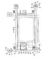
まず、図1及び図2を参照して本発明の一実施形態による有機薄膜トランジスタ表示板について詳細に説明する。
図1は、本発明の一実施形態による有機薄膜トランジスタ表示板の配置図であり、図2は、図1の有機薄膜トランジスタ表示板のII-II線に沿った断面図である。
Example 1
First, an organic thin film transistor array panel according to an embodiment of the present invention will be described in detail with reference to FIGS. 1 and 2.
FIG. 1 is a layout view of an organic thin film transistor array panel according to an embodiment of the present invention, and FIG. 2 is a cross-sectional view taken along line II-II of the organic thin film transistor array panel of FIG.
図示するように、透明なガラスまたはプラスチックなどからなる絶縁基板110上に、複数のゲート線121が形成されている。
ゲート線121はゲート信号を伝達し、第1の方向、主に横方向に延びている。各ゲート線は、上に突出した複数のゲート電極124と他の層または外部駆動回路との接続のために面積が広い端部129を有する。ゲート信号を生成するゲート駆動回路(図示せず)は、基板110上に付着されるフレキシブル印刷回路板(図示せず)上に装着したり、基板110上に直接装着したり、基板110に集積することができる。ゲート駆動回路が基板110上に集積される場合には、ゲート線121が延びてこれと直接接続することができる。
As shown in the drawing, a plurality of
The
ゲート線121は、アルミニウム(Al)とアルミニウム合金などのアルミニウム系金属、銀(Ag)と銀合金などの銀系金属、金(Au)と金合金などの金系金属、銅(Cu)と銅合金などの銅系金属、モリブデン(Mo)とモリブデン合金などのモリブデン系金属、クロム(Cr)、チタニウム(Ti)、タンタル(Ta)などからなることが好ましい。しかし、ゲート線121は、物理的性質が異なる二つの導電膜(図示せず)を含む多重膜構造を有することができる。このうちの一つの導電膜は、信号遅延や電圧降下を減らすために低い比抵抗の金属からなる。これと異なり、もう一つ導電膜は他の物質、特にITO及びIZOとの物理的、化学的、電気的接触特性が優れた物質からなる。ゲート線121は様々の金属及び導電体から形成することができる。
The
ゲート線121の側面は基板110面に対して傾斜しており、その傾斜角は約30°〜80゜であることが好ましい。
ゲート線121上にはゲート絶縁膜140が形成されている。ゲート絶縁膜140は、無機絶縁物または有機絶縁物によって形成することができる。無機絶縁物の例としては、窒化ケイ素(SiNx)及び酸化ケイ素(SiO2)があり、酸化ケイ素の場合、OTS(octadecyl-trichlorosilane)で表面処理してもよい。有機絶縁物の例としては、マレイミドスチレン、ポリビニルフェノール及びm-CEP(Modified Cyanoethylpullulan)がある。
The side surface of the
A
ゲート絶縁膜140上には、複数のデータ線171と複数のドレイン電極175が形成されている。
データ線171はデータ信号を伝達し、第2方向、主に縦方向に延びてゲート線121と交差する。各データ線171は、ゲート電極124に向かって延びた複数のソース電極173と他の層または外部駆動回路との接続のために面積が広い端部179を有する。データ信号を生成するデータ駆動回路(図示せず)は、基板110上に付着されるフレキシブル印刷回路板(図示せず)上に装着したり、基板110上に直接装着したり、基板110に集積することができる。データ駆動回路が基板110上に集積される場合、データ線171が延びてこれと直接接続してもよい。
A plurality of
The
ドレイン電極175は、データ線171と分離されており、ゲート電極124を中心にソース電極173と対向する。
データ線171及びドレイン電極175は、アルミニウム(Al)やアルミニウム合金などアルミニウム系金属、銀(Ag)や銀合金など銀系金属、金(Au)や金合金など金系金属、銅(Cu)や銅合金など銅系金属、モリブデンやモリブデン合金などモリブデン系金属、ニッケル(Ni)、クロム、タンタル(Ta)、チタニウム(Ti)及びITOなどからなることが好ましい。しかし、これらは物理的性質が異なる二つの導電膜(図示せず)を含む多重膜構造を有することも可能である。このうちの一つの導電膜は、信号遅延や電圧降下を減らすために比抵抗が低い金属からなる。これと異なり、もう一つの導電膜は、他の物質、特に有機半導体層、ITO及びIZOとの物理的、化学的、電気的接触特性に優れた物質からなる。データ線171及びドレイン電極175は、これ以外にも様々な金属または導電体によって形成することができる。
The
The
データ線171及びドレイン電極175は、その側面が基板110面に対して30゜〜80゜程度の角度で傾斜していることが好ましい。
ソース電極173、ドレイン電極175及びゲート絶縁膜140上には、複数の島状有機半導体層154が形成されている。有機半導体層154は、ゲート電極124上に位置し、ソース電極173及びドレイン電極175と接続されている。
The side surfaces of the
A plurality of island-shaped
有機半導体層154は、電子を容易に移動させることができる共役構造を有するオリゴマーまたは重合体からなることが好ましい。有機半導体層154は、水溶液及び/又は有機溶媒等に溶解する、つまり、可溶性の化合物であることが好ましい。可溶性の化合物は、低分子化合物又は高分子化合物のいずれでもよく、溶液工程に適用するために、溶解性が低い低分子化合物に親水性または疎水性官能基を結合させた誘導体であってもよい。ここで、溶解する又は可溶性とは、溶液工程で有機半導体層を形成することができる程度に溶解性を有することを意味する。
The
有機半導体層154は、例えば、テトラセンまたはペンタセン等の置換基を含む誘導体、あるいはチオフェン環の2位及び5位を通じて4〜8個が連結されたオリゴチオフェン、ポリチエニレンビニレン、ポリ-3-ヘキシルチオフェン、フタロシアニンまたはチオフェン等から選択して形成することができる。
また、有機半導体層154は感光性を有する有機物質からなる。感光性有機物質は露光により所定のパターンに形成することができ、露光後の生成物は半導体特性を有することが要求される。このような有機物質として、分子構造内に半導体特性を示すことができる部分と、一定の条件下で露光により分解する酸分解基(acid-labile group)とを同時に含有する化合物が挙げられる。このような有機物質が光酸発生剤の存在下で露光される場合、光酸発生剤から放出した酸触媒、例えば、水素触媒(H+)によって酸分解基が分解され、半導体特性を示す有機物質を生成することができる。
The
The
このような感光性有機物質は、蒸着、スピンコーティング、オフセット印刷、スクリーン印刷、マイクロコンタクト印刷またはインクジェット印刷などの方式で全面または部分的に成膜した後、露光して有機半導体層に変換することができる。この場合、比較的低い解像度を示す印刷またはスピンコーティングなどの簡便な方法で形成した有機半導体層を、追加工程なしでフォトエッチングでパターニングすることによって、高解像度の有機半導体層を実現することができる。 Such a photosensitive organic material is formed on the entire surface or a part of the film by a method such as vapor deposition, spin coating, offset printing, screen printing, microcontact printing, or ink jet printing, and then exposed to be converted into an organic semiconductor layer. Can do. In this case, a high-resolution organic semiconductor layer can be realized by patterning an organic semiconductor layer formed by a simple method such as printing or spin coating that exhibits a relatively low resolution by photoetching without an additional step. .
一つのゲート電極124、一つのソース電極173及び一つのドレイン電極175は、有機半導体層154と共に一つの薄膜トランジスタ(TFT)を構成し、薄膜トランジスタのチャンネルは、ソース電極173とドレイン電極175との間の有機半導体層154に形成される。
有機半導体層154上には絶縁パターン164が形成されている。
One
An
絶縁パターン164は、有機半導体層154が外部の熱、プラズマまたは化学物質の影響を受けることを防止するためのもので、パリレン、フッ素系炭化水素化合物またはポリビニルアルコールなどからなることが好ましい。
データ線171、ドレイン電極175及び絶縁パターン164の上には、保護膜180が形成されている。保護膜180は、窒化ケイ素(SiNx)または酸化ケイ素(SiO2)などの無機絶縁物、ポリイミドまたはポリアクリールなどの有機絶縁物、低誘電率絶縁物などからなる。低誘電率絶縁物の誘電定数は4.0以下であることが好ましく、プラズマ化学気相蒸着(PECVD)で形成されるa-Si:C:O、a-Si:O:Fなどがその例である。しかし、保護膜180は、有機膜の優れた絶縁特性を生かしつつ露出した有機半導体層154部分にダメージを与えないように下部無機膜と上部有機膜の二重膜構造を有することができる。ただし、保護膜180を省略することも可能である。
The insulating
A
保護膜180にはデータ線171の端部179及びドレイン電極175をそれぞれ露出させる複数のコンタクトホール182、185が形成されており、保護膜180とゲート絶縁膜140には、ゲート線121の端部129を露出させる複数のコンタクトホール181が形成されている。
保護膜180上には、複数の画素電極191及び複数の接触補助部材81、82が形成されている。これらはITOまたはIZOなどの透明な導電物質やアルミニウム、銀またはその合金などの反射性金属からなることが好ましい。
A plurality of
A plurality of
画素電極191は、コンタクトホール185を介してドレイン電極175と物理的・電気的に接続されており、ドレイン電極175からデータ電圧の印加を受ける。データ電圧が印加された画素電極191は、共通電圧の印加を受ける他の表示板(図示せず)の共通電極(図示せず)と共に電場を生成することで二つの電極間の液晶層(図示せず)の液晶分子の方向を決定する。画素電極191と共通電極は、キャパシタ(以下、液晶キャパシタという。)を構成して薄膜トランジスタが遮断(ターンオフ)された後にも印加された電圧を維持する。
The
画素電極191はゲート線121及びデータ線171と重なって開口率を高める。
接触補助部材81、82はそれぞれコンタクトホール181、182を介してゲート線121の端部129及びデータ線171の端部179に接続されている。接触補助部材81、82は、データ線171及びゲート線121の端部179、129と外部装置との接着性を補完し、これらを保護する。
The
The
次に、図1及び図2に示した有機薄膜トランジスタ表示板を本発明の一実施形態によって製造する方法について、図3〜図13、図1及び図2を参照して説明する。
図3、図5、図8、図10及び図12は、図1及び図2に示した有機薄膜トランジスタ表示板を本発明の一実施形態によって製造する方法の中間工程を示す配置図であり、図4は、図3に示した有機薄膜トランジスタ表示板のIV-IV線に沿った断面図であり、図6は、図5に示した有機薄膜トランジスタ表示板のVI-VI線に沿った断面図であり、図7は、図5及び図6に続く工程を示す断面図であり、図9は、図8に示した有機薄膜トランジスタ表示板のIX-IX線に沿った断面図であり、図11は、図10に示した有機薄膜トランジスタ表示板のXI-XI線に沿った断面図であり、図13は、図12に示した有機薄膜トランジスタ表示板のXIII-XIII線に沿った断面図である。
Next, a method of manufacturing the organic thin film transistor array panel shown in FIGS. 1 and 2 according to an embodiment of the present invention will be described with reference to FIGS. 3 to 13, 1 and 2.
3, 5, 8, 10, and 12 are layout views illustrating intermediate steps of a method of manufacturing the organic thin film transistor array panel shown in FIGS. 1 and 2 according to an embodiment of the present invention. 4 is a cross-sectional view taken along line IV-IV of the organic thin film transistor array panel shown in FIG. 3, and FIG. 6 is a cross-sectional view taken along line VI-VI of the organic thin film transistor array panel shown in FIG. 7 is a cross-sectional view showing a process following FIG. 5 and FIG. 6, FIG. 9 is a cross-sectional view taken along line IX-IX of the organic thin film transistor array panel shown in FIG. 8, and FIG. FIG. 13 is a cross-sectional view taken along line XI-XI of the organic thin film transistor array panel shown in FIG. 10, and FIG. 13 is a cross-sectional view taken along line XIII-XIII of the organic thin film transistor array panel shown in FIG.
まず、図3及び図4に示すように、透明ガラスまたはプラスチックなどの絶縁基板110上に、ゲート電極124と端部129を有する複数のゲート線121を形成する。
次に、図5及び図6に示すように、化学気相蒸着法でゲート絶縁膜140を形成する。ゲート絶縁膜140は約500〜3000Åの厚さを有することが好ましく、OTS溶液に浸して表面処理を施すこともできる。
First, as shown in FIGS. 3 and 4, a plurality of
Next, as shown in FIGS. 5 and 6, a
ゲート絶縁膜140上に金(Au)などの低抵抗導電層を形成した後、フォトエッチング法でパターニングして、ソース電極173及び端部179を有する複数のデータ線171及び複数のドレイン電極175を形成する。
次いで、図7に示すように、データ線171及びドレイン電極175上の全面または部分に、感光性有機物質からなる有機膜150を形成する。ここで、感光性有機物質は、分子構造内に半導体特性を示す部分と露光により分解する酸分解基とを同時に含有するもので、例えば、分子構造内にt−ブチルオキシカルボニル基を含有するペンタセン誘導体が挙げられる。
After a low resistance conductive layer such as gold (Au) is formed over the
Next, as shown in FIG. 7, an
前記ペンタセン誘導体は、ペンタセンとN-スルフィニル-t-ブチルカーバメートとをパラジウム触媒の存在下で反応させることにより形成することができる。この反応は、Diels-Alder反応を行なってペンタセン構造内にt−ブチルオキシカルボニル基を結合させるものである。
前記ペンタセン誘導体は、蒸着、スピンコーティング、オフセット印刷、スクリーン印刷、マイクロコンタクト印刷またはインクジェット印刷などの方式で形成する。
The pentacene derivative can be formed by reacting pentacene with N-sulfinyl-t-butyl carbamate in the presence of a palladium catalyst. In this reaction, a Diels-Alder reaction is performed to bond a t-butyloxycarbonyl group in the pentacene structure.
The pentacene derivative is formed by a method such as vapor deposition, spin coating, offset printing, screen printing, microcontact printing, or ink jet printing.
具体的には、ペンタセン誘導体と水素(H+)触媒を供給するための光酸発生剤として、例えば、ジ−t−ブチル−フェニルヨードニウムパーフルオロブタンスルホネートとを、溶媒中に混合し、スピンコーティングで膜状に形成し、これをUVで露光して約110〜150℃で約5分間熱処理する。この場合、光酸発生剤で生成された水素(H+)触媒によって、ペンタセン誘導体内のt−ブチルオキシカルボニル基が分解されて、図8及び図9に示すように、ペンタセンからなる所定パターンの有機半導体層154が形成される。
Specifically, as a photoacid generator for supplying a pentacene derivative and a hydrogen (H + ) catalyst, for example, di-t-butyl-phenyliodonium perfluorobutanesulfonate is mixed in a solvent, and spin coating is performed. Then, it is exposed to UV and heat-treated at about 110 to 150 ° C. for about 5 minutes. In this case, the t-butyloxycarbonyl group in the pentacene derivative is decomposed by the hydrogen (H + ) catalyst generated by the photoacid generator, and as shown in FIGS. 8 and 9, a predetermined pattern of pentacene is formed. An
続いて、図10及び図11に示すように、常温またはそれよりも低温の乾式工程を用いてパリレン、フッ素系炭化水素化合物またはポリビニルアルコールなどからなる絶縁層を形成する。次いで、絶縁層をフォトエッチング工程でパターニングして有機半導体層154を十分に覆う絶縁パターン164を形成する。
その後、図12及び図13に示すように、データ線171、ドレイン電極175及び絶縁パターン164を覆う保護膜180を積層してパターニングし、ゲート線121の端部129、データ線171の端部179及びドレイン電極175をそれぞれ露出させる複数のコンタクトホール181、182、185を形成する。
Subsequently, as shown in FIGS. 10 and 11, an insulating layer made of parylene, a fluorine-based hydrocarbon compound, polyvinyl alcohol, or the like is formed using a dry process at room temperature or lower than that. Next, the insulating layer is patterned by a photoetching process to form an insulating
Thereafter, as shown in FIGS. 12 and 13, a
最後に、図1及び図2に示すように、保護膜180上に複数の画素電極191と複数の接触部材81、82を形成する。
実施例2
以下、本発明の他の一実施形態による有機薄膜トランジスタ表示板について詳細に説明する。
Finally, as shown in FIGS. 1 and 2, a plurality of
Example 2
Hereinafter, an organic thin film transistor array panel according to another embodiment of the present invention will be described in detail.
図14は、本発明の他の一実施形態による有機薄膜トランジスタ表示板の配置図であり、図15は、図14に示した有機薄膜トランジスタ表示板のXV−XV’線及びXV’−XV”線に沿った断面図である。
透明ガラスまたはプラスチックなどからなる絶縁基板110上に、複数のデータ線171及び光遮断膜174が形成されている。
FIG. 14 is a layout view of an organic thin film transistor array panel according to another embodiment of the present invention, and FIG. 15 is an XV-XV ′ line and an XV′-XV ″ line of the organic thin film transistor array panel shown in FIG. FIG.
A plurality of
データ線171はデータ信号を伝達し、主に縦方向に延びており、各データ線171は横に突出した複数の突出部172と、他の層または外部駆動回路との接続のための広い端部179とを有している。
データ線171及び光遮断膜174は、信号遅延や電圧降下を減らすために低い比抵抗の金属、例えば、金(Au)、銀(Ag)、銅(Cu)、アルミニウム(Al)、またはこれらの合金からなる導電膜からなることが好ましい。また、物理的性質が異なる二つ以上の導電膜を含むことができ、この場合には、一つの導電膜は低抵抗の導電物質からなり、もう一つの導電膜は他の物質、特にIZOまたはITOとの物理的、化学的及び電気的接触特性に優れた物質、例えばモリブデン(Mo)、モリブデン合金(例:モリブデン−タングステン(MoW)合金)またはクロム(Cr)などの導電物質からなることが好ましい。
The data lines 171 transmit data signals and extend mainly in the vertical direction. Each
The
データ線171及び光遮断膜174は、約1000〜3000Åの厚さに形成されている。
データ線171及び光遮断膜174の側面はそれぞれ傾斜しており、その傾斜角は基板110面に対して約30〜80゜であることが好ましい。
データ線171及び光遮断膜174の上には、窒化ケイ素(SiNx)または酸化ケイ素(SiO2)などの無機絶縁物質からなる下部層間絶縁膜160pと、耐久性に優れたポリアクリル、ポリイミド及び/またはベンゾシクロブテン(C10H8)などを含む有機絶縁物質からなる上部層間絶縁膜160qが順次に形成されている。場合によって、下部層間絶縁膜160p及び上部層間絶縁膜160qのうちいずれか一つを省略することも可能である。
The
The side surfaces of the
On the
下部層間絶縁膜160p及び上部層間絶縁膜160qには、データ線171の突出部172及び端部179をそれぞれ露出させる複数のコンタクトホール163、162が形成されている。
上部層間絶縁膜160q上に、ゲート信号を伝達する複数のゲート線121、データ線171上部に形成されている接触パターン128及び複数の維持電極線131が形成されている。
In the lower
A plurality of
ゲート線121はゲート信号を伝達し、主に縦方向に延びたデータ線171と交差する。また、ゲート線121の一部は上に突出して複数のゲート電極124を構成し、ゲート線121の一端部129は、外部回路または他の層との接続のために幅が拡張されている。
接触パターン128は、下部で層間絶縁膜160に形成されたコンタクトホール163を介してデータ線171に接続されており、上部でゲート絶縁膜140に形成されたコンタクトホール143を介してソース電極193に接続されている。データ線171とソース電極193との間には、上部層間絶縁膜160q及びゲート絶縁膜140を有する複数の有機膜が設けられているので、有機膜によってデータ線171とソース電極193との間に接触不良が生じるおそれがある。よって、データ線171とソース電極193との間に接触パターン128を介在させることで、データ線171とソース電極193との間の接触不良を防止することができる。
The
The
維持電極線131のそれぞれは主に横方向に延びており、ゲート線121とデータ線171で囲まれた領域の周縁に配置されている維持電極133を含む。
ゲート線121、接触パターン128及び維持電極線131は、信号の遅延や電圧降下を減らすために低い比抵抗の金属、例えば金(Au)、銀(Ag)、アルミニウム(Al)またはこれらの合金などからなる導電膜を含むことが望ましい。または、物理的性質が異なる二つ以上の導電膜を含むことができ、この場合、一つの導電膜は低抵抗の導電物質からなり、もう一つの導電膜は他の物質、特にIZOまたはITOとの物理的、化学的及び電気的接触特性に優れた物質、例えばモリブデン(Mo)、モリブデン合金(例:モリブデン−タングステン(MoW)合金)またはクロム(Cr)などの導電物質からなることが好ましい。
Each of the
The
ゲート線121、接触パターン128及び維持電極線131の側面はそれぞれ傾斜しており、その傾斜角は基板110面に対して約30〜80°であることが好ましい。
ゲート線121、接触パターン128及び維持電極線131を含んだ全面に窒化ケイ素(SiNx)などの無機絶縁物質または有機絶縁物質からなるゲート絶縁膜140が形成されている。ここで、ゲート絶縁膜140は有機物質からなることが好ましく、例えば、オクタデシルトリクロロシラン(OTS)で表面処理された酸化ケイ素(SiO2)または真空中に化学気相蒸着(CVD)工程によって形成されるパリレンまたはフッ素(F)含有の炭化水素系の高分子化合物から形成することができる。
The side surfaces of the
A
特に、パリレンは塗布均一性が非常に優れており、1000Åから数μmまで塗布厚さを容易に調節でき、誘電率が非常に低くて絶縁膜としての特性が優れている。また、パリレンが高分子化される場合、現存する全ての有機溶媒にほとんど溶解されず、常温で蒸着可能であるため、熱ストレスがないという利点がある。さらに、乾式工程で形成されて別途の溶剤が不要で、環境親和的である。 In particular, parylene is very excellent in coating uniformity, the coating thickness can be easily adjusted from 1000 mm to several μm, the dielectric constant is very low, and the characteristics as an insulating film are excellent. Further, when parylene is polymerized, there is an advantage that there is no thermal stress because it is hardly dissolved in all existing organic solvents and can be deposited at room temperature. Furthermore, it is formed by a dry process and does not require a separate solvent, and is environmentally friendly.
ゲート絶縁膜140は、約6000Å〜1.2μmの厚さに形成されている。
ゲート絶縁膜140には、ゲート線121の端部129及びデータ線171の端部179をそれぞれ露出させるコンタクトホール141、142と、層間絶縁膜160のコンタクトホール163と共にゲート電極124に隣接したデータ線171を露出させる複数のコンタクトホール143が形成されている。
The
The
ゲート絶縁膜140にゲート線121及びデータ線171の端部129、179を露出させるコンタクトホール141、142が形成されている場合には、外部の駆動回路を異方性導電膜を利用してゲート線121及びデータ線171に接続するためゲート線121及びデータ線171が接触部を有する構造である。また、基板110上部に直接ゲート駆動回路を、有機薄膜トランジスタと同一層で形成することができる。この場合、ゲート線121及びデータ線171の端部129、179は駆動回路の出力端に電気的に接続される。
When contact holes 141 and 142 exposing the
ゲート絶縁膜140上には、複数のソース電極193及び複数の画素電極191と、複数の接触補助部材81、82が形成されている。
ソース電極193、画素電極191及び接触補助部材81、82は、IZOまたはITOなどのような透明な導電物質または反射度が高い導電物質から、約300〜800Åの厚さに形成することができる。
A plurality of
The
画素電極191のうちゲート電極124上部に位置する一部はドレイン電極195を構成し、データ信号の印加を受ける。
ソース電極193は、ゲート電極124を中心にドレイン電極195と対向し、コンタクトホール143、163を介してデータ線171に接続されている。
ソース電極193とドレイン電極195は、互いに平行に対向する境界線を有するが、単位面積で長さを極大化するために屈曲されている。
A part of the
The source electrode 193 faces the
The
また、画素電極191は、隣接するゲート線121及びデータ線171と重なって開口率を高めているが、重ならないこともある。
接触補助部材81、82は、コンタクトホール141、142を介してゲート線121及びデータ線171の端部129、179にそれぞれ接続される。接触補助部材81、82は、ゲート線121及びデータ線171の各端部129、179と駆動集積回路のような外部装置との接着性を補完し、これらを保護する役割を果たすもので必須ではなく、これらの適用は選択的である。
The
The
画素電極191及びソース電極193上には、複数の島状有機半導体層154が形成されている。有機半導体層154はゲート電極124上に位置し、ソース電極193及びドレイン電極195と接続されている。有機半導体層154の下部には光遮断膜174が形成されている。光遮断膜174は、有機半導体層154で光による漏洩電流が急激に増加することを防止する役割を果たす。
A plurality of island-like organic semiconductor layers 154 are formed on the
有機半導体層154は、電子を容易に移動させることができる共役構造を有するオリゴマーまたは重合体からなることが好ましい。有機半導体層154は、低分子化合物または水溶液や有機溶媒に溶解される高分子化合物からなることが好ましく、溶解性が低い低分子化合物を、溶液工程に適用するために、低分子共役化合物に親水性または疎水性官能基を結合させた誘導体を用いて形成してもよい。
The
有機半導体層154としては、例えばテトラセンまたはペンタセンの置換基を含む誘導体であるか、チオフェン環の2、5位置を通じて4〜8個が連結されたオリゴチオフェン、ポリチエニレンビニレン、ポリ−3−ヘキシルチオフェン、フタロシアニンまたはチオフェン等から選択することができる。
また、有機半導体層154は感光性を有する有機物質からなる。感光性有機物質は露光により所定のパターンに形成することができ、露光後の生成物は半導体特性を有する必要がある。このような有機物質として、分子構造内に半導体特性を示すことができる部分と、一定の条件下で露光により分解する酸分解基とを同時に含有する化合物がある。このような有機物質は、光酸発生剤の存在下で露光される場合、光酸発生剤から放出された酸触媒(例えば、H+)により酸分解基が分解して半導体特性を示す有機物質が生成され得る。
The
The
このような感光性有機物質は、蒸着、スピンコーティング、オフセット印刷、スクリーン印刷、マイクロコンタクト印刷またはインクジェット印刷などの方式で全面または部分的に形成された後、露光して有機半導体層に形成されることが好ましい。この場合、比較的低い解像度を示す印刷またはスピンコーティングなどの簡単な方法で形成した有機半導体層を、別途の追加工程なしでフォトエッチングでパターニングすることにより、高解像度の有機半導体層を実現することができる。 Such a photosensitive organic material is formed on the organic semiconductor layer after being formed entirely or partially by a method such as vapor deposition, spin coating, offset printing, screen printing, microcontact printing, or ink jet printing. It is preferable. In this case, a high-resolution organic semiconductor layer can be realized by patterning an organic semiconductor layer formed by a simple method such as printing or spin coating showing a relatively low resolution by photoetching without any additional process. Can do.
有機半導体層154は、約300〜1000Åの厚さに形成されることが好ましい。
一つのゲート電極124、一つのソース電極193及び一つのドレイン電極195は、有機半導体層154と共に一つの薄膜トランジスタ(TFT)を構成し、薄膜トランジスタのチャンネル(Q)はソース電極193とドレイン電極195との間の有機半導体層154に形成される。
The
One
有機半導体層154上には絶縁パターン183が形成されている。
絶縁パターン183は、有機半導体層154が外部熱、プラズマまたは化学物質の影響を受けることを防止するためのもので、パリレン、フッ素系炭化水素化合物またはポリビニルアルコールなどで形成されることが好ましい。
以下、図14及び図15に示した有機薄膜トランジスタ表示板を本発明の一実施形態によって製造する方法について図16〜図24を参照して詳細に説明する。
An
The insulating
Hereinafter, a method of manufacturing the organic thin film transistor array panel shown in FIGS. 14 and 15 according to an embodiment of the present invention will be described in detail with reference to FIGS.
図16、図18、図20及び図23は、図14及び図15に示した有機薄膜トランジスタ表示板を本発明の一実施形態によって製造する方法の中間工程の配置図であり、図17は、図16に示した有機薄膜トランジスタ表示板のXVII−XVII’−XVII線に沿った断面図であり、図19は、図18に示したXIX−XIX’−XIX線に沿った断面図であり、図21は、図20に示したXXI−XXI’−XXI線に沿った断面図であり、図22は、図21に続く工程を示す断面図であり、図24は、図23に示した有機薄膜トランジスタ表示板のXXIV−XXIV’−XXIV線に沿った断面図である。 16, 18, 20, and 23 are layout views of intermediate steps of a method for manufacturing the organic thin film transistor array panel shown in FIGS. 14 and 15 according to an embodiment of the present invention. FIG. 19 is a cross-sectional view taken along line XVII-XVII′-XVII of the organic thin film transistor array panel shown in FIG. 16, and FIG. 19 is a cross-sectional view taken along line XIX-XIX′-XIX shown in FIG. FIG. 22 is a sectional view taken along line XXI-XXI′-XXI shown in FIG. 20, FIG. 22 is a sectional view showing a step following FIG. 21, and FIG. 24 is an organic thin film transistor display shown in FIG. It is sectional drawing along the XXIV-XXIV'-XXIV line of the board.
まず、図16及び図17に示すように、透明ガラスまたはプラスチックなどの絶縁基板110上に、スパッタリングで金属層を形成する。
ここで、金属層は、低い比抵抗の金属、例えば、金(Au)、銀(Ag)、銅(Cu)、アルミニウム(Al)またはこれらの合金からなる導電体からなることが好ましく、低抵抗特性及び接着性などを考慮して多層に形成することも可能である。
First, as shown in FIGS. 16 and 17, a metal layer is formed by sputtering on an insulating
Here, the metal layer is preferably made of a low resistivity metal such as a conductor made of gold (Au), silver (Ag), copper (Cu), aluminum (Al), or an alloy thereof. It is also possible to form a multilayer in consideration of characteristics and adhesiveness.
その後、金属層をフォトエッチングして、突出部172及び端部179を含むデータ線171と光遮断膜174を形成する。
次に、図18及び図19に示すように、データ線171及び光遮断膜174を含む基板全面に窒化ケイ素(SiNx)などの無機物質からなる下部層間絶縁膜160pと感光性有機物質からなる上部層間絶縁膜160qを順次に形成する。ここで、下部層間絶縁膜160pは、約250〜400℃の温度で化学気相蒸着(CVD)法で形成し、上部層間絶縁膜160qはスピンコーティングのような溶液工程で形成することが好ましい。場合によって、下部層間絶縁膜160p及び上部層間絶縁膜160qのうちのいずれか一つを省略することも可能である。
Thereafter, the metal layer is photoetched to form the
Next, as shown in FIGS. 18 and 19, a lower
その後、感光性有機物質からなる上部層間絶縁膜160qを露光してデータ線171の突出部172及び端部179をそれぞれ露出させるコンタクトホール162、163を形成した後、上部層間絶縁膜160qをマスクとして下部層間絶縁膜160pを乾式エッチングする。
次いで、上部層間絶縁膜160q上に金属層を形成する。金属層は、例えば、金(Au)、銀(Ag)、銅(Cu)、アルミニウム(Al)またはこれらの合金からなる導電体からなることが好ましく、低抵抗特性及び接着性などを考慮して多層に形成することも可能である。
Thereafter, the upper
Next, a metal layer is formed on the upper
次に、金属層をフォトエッチングして、ゲート電極124を含むゲート線121、接触パターン128及び維持電極133を含む維持電極線131を形成する。
図20及び図21に示すように、ゲート線121、接触パターン128及び維持電極線131を含む全面に無機物質または感光性有機物質からなるゲート絶縁膜140を形成する。
Next, the metal layer is photoetched to form the
20 and 21, a
その後、ゲート絶縁膜140を露光してゲート線121の端部129、データ線171の端部179及びデータ線171の突出部172をそれぞれ露出させるコンタクトホール141、142、143を形成する。
次いで、ゲート絶縁膜140の全面にITOをスパッタリングする。この時、スパッタリングは常温で行い非晶質ITO膜を形成する。その後、前記非晶質ITO膜をアミン(NH2)成分が含まれている弱塩基性エッチング液を利用してパターニングして、ドレイン電極195を含む画素電極191、ソース電極193及び接触補助部材81、82を形成する。このように、非晶質ITOで形成する場合、弱塩基性エッチング液で容易にエッチングすることができるため、他の導電体または結晶質ITOのように強酸エッチング液が不要である。強酸エッチング液を利用してパターニングする場合、エッチング液が下部のゲート絶縁膜140と接触して不良を起こすおそれもあり、ゲート絶縁膜140に発生したクラックに浸透して下部導電層を侵食する可能性もある。
Thereafter, the
Next, ITO is sputtered on the entire surface of the
非晶質ITOをそのまま利用してもよく、非晶質ITOを結晶化して結晶質ITOを形成することも可能である。
前記実施形態ではITOについてのみ説明したが、IZOのような他の透明電極または金(Au)、アルミニウム(Al)のような反射性電極で形成することもできる。
次に、図22に示すように、ソース電極193及び画素電極191を含んだ全面に感光性有機物質からなる有機膜150を形成する。ここで、感光性有機物質は、分子構造内に半導体特性を示す部分と露光により分解する酸分解基とを同時に含有するもので、例えば、分子構造内にt−ブチルオキシカルボニル基を含有するペンタセン誘導体がある。
Amorphous ITO may be used as it is, and crystalline ITO can be formed by crystallizing amorphous ITO.
Although only the ITO has been described in the above embodiment, it may be formed of another transparent electrode such as IZO or a reflective electrode such as gold (Au) or aluminum (Al).
Next, as shown in FIG. 22, an
前記ペンタセン誘導体は、ペンタセンとN−スルフィニル−t−ブチルカーバメートをパラジウム触媒の存在下で反応させることが望ましい。前記反応は、Diels-Alder反応によってペンタセン構造内にt−ブチルオキシカルボニル基を結合させるものである。
前記ペンタセン誘導体を蒸着、スピンコーティング、オフセット印刷、スクリーン印刷、マイクロコンタクト印刷またはインクジェット印刷などの方法で形成する。
The pentacene derivative is preferably reacted with pentacene and N-sulfinyl-t-butyl carbamate in the presence of a palladium catalyst. In the above reaction, a t-butyloxycarbonyl group is bonded to the pentacene structure by Diels-Alder reaction.
The pentacene derivative is formed by a method such as vapor deposition, spin coating, offset printing, screen printing, microcontact printing, or ink jet printing.
その後、水素(H+)触媒を供給するための光酸発生剤として、例えば、ジ−t−ブチル−フェニルヨードニウムパーフルオロブタンスルホネートの存在下、前記ペンタセン誘導体をUVで露光して約110〜150℃で約5分間熱処理する。この場合、光酸発生剤で生成された水素(H+)触媒によってペンタセン誘導体内のt−ブチルオキシカルボニル基が分解されて、図23及び図24に示すように、ペンタセンからなる所定のパターンの有機半導体層154が形成される。
Thereafter, as a photoacid generator for supplying a hydrogen (H + ) catalyst, for example, the pentacene derivative is exposed to UV in the presence of di-t-butyl-phenyliodonium perfluorobutane sulfonate for about 110 to 150. Heat treatment is performed at a temperature of about 5 minutes. In this case, the t-butyloxycarbonyl group in the pentacene derivative is decomposed by the hydrogen (H +) catalyst generated by the photoacid generator, and as shown in FIG. 23 and FIG. A
最後に、図14及び図15のように、常温またはそれよりも低温の乾式工程でパリレン、フッ素系炭化水素化合物またはポリビニルアルコールなどの絶縁層を形成する。次いで、絶縁層をフォトエッチング工程でパターニングして有機半導体層154を十分に覆う絶縁パターン183を形成する。
以上、本発明の好ましい実施例について詳細に説明したが、本発明の権利範囲はこれに限定されず、請求の範囲で定義している本発明の基本概念を利用した当業者の多様な変形及び改良形態も本発明の権利範囲に属するものである。
Finally, as shown in FIGS. 14 and 15, an insulating layer such as parylene, a fluorine-based hydrocarbon compound, or polyvinyl alcohol is formed by a dry process at room temperature or lower temperature. Next, the insulating layer is patterned by a photoetching process to form an insulating
The preferred embodiments of the present invention have been described in detail above, but the scope of the present invention is not limited thereto, and various modifications and variations of those skilled in the art using the basic concept of the present invention defined in the claims. Improvements are also within the scope of the present invention.
本発明は、液晶表示装置用薄膜トランジスタ表示板のみならず、例えば、有機発光表示装置(OLED)及び電子紙(e−paper)のように、薄膜トランジスタにより駆動できる他の表示装置にも同様に適用することができる。 The present invention applies not only to a thin film transistor panel for a liquid crystal display, but also to other display devices that can be driven by a thin film transistor, such as an organic light emitting display (OLED) and electronic paper (e-paper). be able to.
110 絶縁基板
121 ゲート線
124 ゲート電極
140 ゲート絶縁膜
171 データ線
175 ドレイン電極
173 ソース電極
154 有機半導体層
164 絶縁パターン
180 保護膜
181、182、185 コンタクトホール
191 画素電極
81、82 接触補助部材
174 光遮断膜
163、162 コンタクトホール
128 接触パターン
131 維持電極線
160 層間絶縁膜
141、142、143 コンタクトホール
193 ソース電極
195 ドレイン電極
183 絶縁パターン
150 有機膜
110 Insulating
Claims (30)
第1方向に延びた複数のゲート線と、
前記ゲート線と絶縁されて交差し、第2方向に延びた複数のデータ線と、
前記データ線に接続されているソース電極と、
前記ソース電極と対向するドレイン電極と、
前記ドレイン電極に接続されている画素電極と、
前記ソース電極と前記ドレイン電極とに接続されており、感光性を有する有機物質からなる有機半導体層とを備えることを特徴とする有機薄膜トランジスタ表示板。 A substrate,
A plurality of gate lines extending in a first direction;
A plurality of data lines insulated from and intersecting the gate lines and extending in a second direction;
A source electrode connected to the data line;
A drain electrode facing the source electrode;
A pixel electrode connected to the drain electrode;
An organic thin film transistor array panel, comprising: an organic semiconductor layer made of an organic material having photosensitivity, connected to the source electrode and the drain electrode.
前記ゲート線上にゲート絶縁膜を形成する工程と、
前記ゲート絶縁膜上にソース電極を有するデータ線及びドレイン電極を形成する工程と、
前記データ線及び前記ドレイン電極上に感光性有機物質を形成する工程と、
前記感光性有機物質を露光して有機半導体層を形成する工程と、
前記有機半導体層を覆う絶縁パターンを形成する工程と、
前記ドレイン電極に接続される画素電極を形成する工程とを含むことを特徴とする有機薄膜トランジスタ表示板の製造方法。 Forming a gate line on the substrate;
Forming a gate insulating film on the gate line;
Forming a data line and a drain electrode having a source electrode on the gate insulating film;
Forming a photosensitive organic material on the data line and the drain electrode;
Exposing the photosensitive organic material to form an organic semiconductor layer;
Forming an insulating pattern covering the organic semiconductor layer;
Forming a pixel electrode connected to the drain electrode, and a method of manufacturing an organic thin film transistor array panel.
前記有機半導体層上に絶縁層を形成する工程と、
前記絶縁層をフォトエッチングでパターニングする工程とを含む請求項13に記載の有機薄膜トランジスタ表示板の製造方法。 The step of forming the insulating pattern includes:
Forming an insulating layer on the organic semiconductor layer;
The method of manufacturing an organic thin film transistor array panel according to claim 13, further comprising: patterning the insulating layer by photoetching.
前記データ線上に絶縁膜を形成する工程と、
前記絶縁膜上にゲート線を形成する工程と、
前記ゲート線上に、前記データ線を露出させるコンタクトホールを含むゲート絶縁膜を形成する工程と、
前記ゲート絶縁膜上に、前記コンタクトホールを介して前記データ線に接続されるソース電極及び前記ソース電極と対向するドレイン電極を含む画素電極を形成する工程と、
前記ソース電極及び前記画素電極上に感光性有機物質を形成する工程と、
前記感光性有機物質を露光して有機半導体層を形成する工程と、
前記有機半導体層を覆う絶縁パターンを形成する工程とを含む有機薄膜トランジスタ表示板の製造方法。 Forming a plurality of data lines on the substrate;
Forming an insulating film on the data line;
Forming a gate line on the insulating film;
Forming a gate insulating film including a contact hole exposing the data line on the gate line;
Forming a pixel electrode including a source electrode connected to the data line through the contact hole and a drain electrode facing the source electrode on the gate insulating film;
Forming a photosensitive organic material on the source electrode and the pixel electrode;
Exposing the photosensitive organic material to form an organic semiconductor layer;
Forming an insulating pattern that covers the organic semiconductor layer.
Applications Claiming Priority (1)
| Application Number | Priority Date | Filing Date | Title |
|---|---|---|---|
| KR1020050037082A KR101219035B1 (en) | 2005-05-03 | 2005-05-03 | Organic thin film transistor array panel and method for manufacturing the same |
Publications (2)
| Publication Number | Publication Date |
|---|---|
| JP2006313913A true JP2006313913A (en) | 2006-11-16 |
| JP2006313913A5 JP2006313913A5 (en) | 2009-06-04 |
Family
ID=36943764
Family Applications (1)
| Application Number | Title | Priority Date | Filing Date |
|---|---|---|---|
| JP2006129039A Pending JP2006313913A (en) | 2005-05-03 | 2006-05-08 | Organic thin film transistor indication plate and its manufacturing method |
Country Status (5)
| Country | Link |
|---|---|
| US (2) | US20060197884A1 (en) |
| JP (1) | JP2006313913A (en) |
| KR (1) | KR101219035B1 (en) |
| CN (1) | CN100517744C (en) |
| TW (1) | TWI434446B (en) |
Cited By (5)
| Publication number | Priority date | Publication date | Assignee | Title |
|---|---|---|---|---|
| JP2008270744A (en) * | 2007-03-28 | 2008-11-06 | Toppan Printing Co Ltd | Thin-film transistor array, manufacturing method of thin-film transistor array, and active matrix display |
| JP2011071501A (en) * | 2009-08-24 | 2011-04-07 | Ricoh Co Ltd | Method for manufacturing organic electronic device and organic electronic device |
| KR20120094575A (en) * | 2011-02-17 | 2012-08-27 | 삼성전자주식회사 | Display substrate and method of manufacturing the display substrate |
| JP2013531884A (en) * | 2010-05-28 | 2013-08-08 | コーニング インコーポレイテッド | Reinforced semiconductor device using photoactive organic material and method for manufacturing the same |
| JP2014512108A (en) * | 2011-04-21 | 2014-05-19 | シーピーアイ イノベーション サービシズ リミテッド | Transistor |
Families Citing this family (16)
| Publication number | Priority date | Publication date | Assignee | Title |
|---|---|---|---|---|
| KR20070053060A (en) * | 2005-11-19 | 2007-05-23 | 삼성전자주식회사 | Display device and manufacturing method thereof |
| US8138075B1 (en) | 2006-02-06 | 2012-03-20 | Eberlein Dietmar C | Systems and methods for the manufacture of flat panel devices |
| KR101197059B1 (en) * | 2006-07-11 | 2012-11-06 | 삼성디스플레이 주식회사 | Thin film transistor array panel and method for manufacturing the same |
| JP2010040897A (en) * | 2008-08-07 | 2010-02-18 | Sony Corp | Organic thin film transistor, production method thereof, and electronic device |
| KR20130011856A (en) * | 2011-07-22 | 2013-01-30 | 삼성디스플레이 주식회사 | Display panel and fabrication method thereof |
| DE102011052583A1 (en) | 2011-08-11 | 2013-02-14 | Hella Kgaa Hueck & Co. | Light module for an outdoor light |
| KR101774491B1 (en) | 2011-10-14 | 2017-09-13 | 삼성전자주식회사 | Organic pixel including organic photodiode, manufacturing method thereof, and apparatuses including the same |
| US9366905B2 (en) * | 2011-12-05 | 2016-06-14 | Shenzhen China Star Optoelectronics Technology Co., Ltd. | Liquid crystal panel and manufacturing method for the same |
| US20140036188A1 (en) * | 2012-08-01 | 2014-02-06 | Cheng-Hung Chen | Liquid Crystal Display Device, Array Substrate and Manufacturing Method Thereof |
| KR102027361B1 (en) * | 2013-02-13 | 2019-10-01 | 삼성전자주식회사 | Thin film transistor panel and method of manufacturing the same and electronic device including the thin film transistor panel |
| CN103383946B (en) | 2013-07-12 | 2016-05-25 | 京东方科技集团股份有限公司 | The preparation method of a kind of array base palte, display unit and array base palte |
| GB2519081B (en) * | 2013-10-08 | 2019-07-03 | Flexenable Ltd | Electronic devices including organic materials |
| CN104091886B (en) * | 2014-07-04 | 2016-11-23 | 京东方科技集团股份有限公司 | A kind of OTFT, array base palte and preparation method, display device |
| CN106876415B (en) * | 2017-03-20 | 2019-09-10 | 上海天马微电子有限公司 | A kind of thin-film transistor array base-plate and its manufacturing method |
| CN111725242B (en) * | 2020-06-30 | 2022-09-02 | 京东方科技集团股份有限公司 | Array substrate, preparation method thereof and display device |
| CN113193031B (en) * | 2021-04-29 | 2022-10-04 | Tcl华星光电技术有限公司 | Display panel and display device |
Citations (6)
| Publication number | Priority date | Publication date | Assignee | Title |
|---|---|---|---|---|
| JP2001148483A (en) * | 1999-09-30 | 2001-05-29 | Internatl Business Mach Corp <Ibm> | High performance thin film transistor for flat panel display and active matrix process |
| JP2001244467A (en) * | 2000-02-28 | 2001-09-07 | Hitachi Ltd | Coplanar semiconductor device, display device using it, and method for its manufacture |
| JP2003202587A (en) * | 2001-12-28 | 2003-07-18 | Sanyo Electric Co Ltd | Display device and method of manufacturing the same |
| US20040119073A1 (en) * | 2002-12-20 | 2004-06-24 | International Business Machines Corporation | Synthesis and application of photosensitive pentacene precursor in organic thin film transistors |
| JP2004260057A (en) * | 2003-02-27 | 2004-09-16 | Konica Minolta Holdings Inc | Organic thin film transistor, and manufacturing method thereof |
| WO2004100282A2 (en) * | 2003-05-12 | 2004-11-18 | Cambridge University Technical Services Limited | Manufacture of a polymer device |
Family Cites Families (23)
| Publication number | Priority date | Publication date | Assignee | Title |
|---|---|---|---|---|
| US6087196A (en) * | 1998-01-30 | 2000-07-11 | The Trustees Of Princeton University | Fabrication of organic semiconductor devices using ink jet printing |
| JP4948726B2 (en) * | 1999-07-21 | 2012-06-06 | イー インク コーポレイション | Preferred method of making an electronic circuit element for controlling an electronic display |
| US6882045B2 (en) * | 1999-10-28 | 2005-04-19 | Thomas J. Massingill | Multi-chip module and method for forming and method for deplating defective capacitors |
| GB2373095A (en) | 2001-03-09 | 2002-09-11 | Seiko Epson Corp | Patterning substrates with evaporation residues |
| GB0112611D0 (en) | 2001-05-23 | 2001-07-18 | Plastic Logic Ltd | Patterning of devices |
| GB0116735D0 (en) | 2001-07-09 | 2001-08-29 | Plastic Logic Ltd | Alignment of polymers |
| EP1282175A3 (en) * | 2001-08-03 | 2007-03-14 | FUJIFILM Corporation | Conductive pattern material and method for forming conductive pattern |
| GB2379083A (en) * | 2001-08-20 | 2003-02-26 | Seiko Epson Corp | Inkjet printing on a substrate using two immiscible liquids |
| KR100961251B1 (en) | 2001-10-01 | 2010-06-03 | 코닌클리케 필립스 일렉트로닉스 엔.브이. | Composition, electronic device and method of manufacturing the electronic device |
| JP2003229579A (en) | 2001-11-28 | 2003-08-15 | Konica Corp | Field effect transistor and manufacturing method therefor |
| JP4360801B2 (en) | 2001-12-25 | 2009-11-11 | シャープ株式会社 | Transistor and display device using the same |
| KR100774258B1 (en) | 2001-12-27 | 2007-11-08 | 엘지.필립스 엘시디 주식회사 | Ink-jetting type Space for Liquid Crystal Display Device |
| JP2003318190A (en) | 2002-04-22 | 2003-11-07 | Seiko Epson Corp | Method for manufacturing semiconductor device, method for manufacturing electrooptical device and electronic device |
| JP2004031933A (en) | 2002-05-09 | 2004-01-29 | Konica Minolta Holdings Inc | Method for manufacturing organic thin-film transistor, and organic thin-film transistor and organic transistor sheet manufactured using the same |
| GB2388709A (en) | 2002-05-17 | 2003-11-19 | Seiko Epson Corp | Circuit fabrication method |
| GB2391385A (en) | 2002-07-26 | 2004-02-04 | Seiko Epson Corp | Patterning method by forming indent region to control spreading of liquid material deposited onto substrate |
| JP2004273982A (en) | 2003-03-12 | 2004-09-30 | Konica Minolta Holdings Inc | Method for manufacturing thin film transistor sheet |
| JP4713818B2 (en) | 2003-03-28 | 2011-06-29 | パナソニック株式会社 | Organic transistor manufacturing method and organic EL display device manufacturing method |
| KR20050029426A (en) * | 2003-09-22 | 2005-03-28 | 삼성에스디아이 주식회사 | Full color oled having color filter layer or color conversion medium |
| CN1605916B (en) * | 2003-10-10 | 2010-05-05 | 乐金显示有限公司 | Liquid crystal display panel having the thin film transistor array substrate, and method of manufacturing thin film transistor array substrate and liquid crystal display panel |
| JP4385812B2 (en) * | 2004-03-26 | 2009-12-16 | 株式会社日立製作所 | Thin film transistor and manufacturing method thereof |
| KR100635565B1 (en) * | 2004-06-29 | 2006-10-17 | 삼성에스디아이 주식회사 | Fabricating method of OLED and the device |
| JP4349307B2 (en) * | 2005-03-16 | 2009-10-21 | セイコーエプソン株式会社 | Organic semiconductor device manufacturing method, organic semiconductor device, electronic device, and electronic apparatus |
-
2005
- 2005-05-03 KR KR1020050037082A patent/KR101219035B1/en active IP Right Grant
-
2006
- 2006-05-03 US US11/416,968 patent/US20060197884A1/en not_active Abandoned
- 2006-05-03 TW TW095115747A patent/TWI434446B/en active
- 2006-05-08 CN CNB2006100886658A patent/CN100517744C/en active Active
- 2006-05-08 JP JP2006129039A patent/JP2006313913A/en active Pending
-
2010
- 2010-09-24 US US12/889,613 patent/US8293569B2/en not_active Expired - Fee Related
Patent Citations (7)
| Publication number | Priority date | Publication date | Assignee | Title |
|---|---|---|---|---|
| JP2001148483A (en) * | 1999-09-30 | 2001-05-29 | Internatl Business Mach Corp <Ibm> | High performance thin film transistor for flat panel display and active matrix process |
| JP2001244467A (en) * | 2000-02-28 | 2001-09-07 | Hitachi Ltd | Coplanar semiconductor device, display device using it, and method for its manufacture |
| JP2003202587A (en) * | 2001-12-28 | 2003-07-18 | Sanyo Electric Co Ltd | Display device and method of manufacturing the same |
| US20040119073A1 (en) * | 2002-12-20 | 2004-06-24 | International Business Machines Corporation | Synthesis and application of photosensitive pentacene precursor in organic thin film transistors |
| JP2004260057A (en) * | 2003-02-27 | 2004-09-16 | Konica Minolta Holdings Inc | Organic thin film transistor, and manufacturing method thereof |
| WO2004100282A2 (en) * | 2003-05-12 | 2004-11-18 | Cambridge University Technical Services Limited | Manufacture of a polymer device |
| JP2007527542A (en) * | 2003-05-12 | 2007-09-27 | ケンブリッジ エンタープライズ リミティド | Manufacture of polymer devices |
Cited By (6)
| Publication number | Priority date | Publication date | Assignee | Title |
|---|---|---|---|---|
| JP2008270744A (en) * | 2007-03-28 | 2008-11-06 | Toppan Printing Co Ltd | Thin-film transistor array, manufacturing method of thin-film transistor array, and active matrix display |
| JP2011071501A (en) * | 2009-08-24 | 2011-04-07 | Ricoh Co Ltd | Method for manufacturing organic electronic device and organic electronic device |
| JP2013531884A (en) * | 2010-05-28 | 2013-08-08 | コーニング インコーポレイテッド | Reinforced semiconductor device using photoactive organic material and method for manufacturing the same |
| KR20120094575A (en) * | 2011-02-17 | 2012-08-27 | 삼성전자주식회사 | Display substrate and method of manufacturing the display substrate |
| JP2014512108A (en) * | 2011-04-21 | 2014-05-19 | シーピーアイ イノベーション サービシズ リミテッド | Transistor |
| US10090482B2 (en) | 2011-04-21 | 2018-10-02 | Cpi Innovation Services Limited | Transistors |
Also Published As
| Publication number | Publication date |
|---|---|
| KR20060114889A (en) | 2006-11-08 |
| US8293569B2 (en) | 2012-10-23 |
| TW200703735A (en) | 2007-01-16 |
| CN100517744C (en) | 2009-07-22 |
| KR101219035B1 (en) | 2013-01-07 |
| TWI434446B (en) | 2014-04-11 |
| US20060197884A1 (en) | 2006-09-07 |
| CN1870284A (en) | 2006-11-29 |
| US20110014736A1 (en) | 2011-01-20 |
Similar Documents
| Publication | Publication Date | Title |
|---|---|---|
| JP2006313913A (en) | Organic thin film transistor indication plate and its manufacturing method | |
| US7919778B2 (en) | Making organic thin film transistor array panels | |
| US7838872B2 (en) | Organic thin film transistor array panel | |
| US7768000B2 (en) | Thin film transistor array panel and manufacturing method thereof | |
| KR101326129B1 (en) | Organic thin film transistor array panel and method for manufacturing the same | |
| US20070024766A1 (en) | Organic thin film transistor display panel | |
| KR20060098522A (en) | Organic thin film transistor array panel and method for manufacturing the same | |
| JP2007140520A (en) | Organic thin film transistor display plate and its manufacturing method | |
| US20060223222A1 (en) | Organic thin film transistor array panel and method of manufacturing the same | |
| US7915074B2 (en) | Thin film transistor array panel and manufacturing method thereof | |
| US8399311B2 (en) | Thin film transistor array panel and method of manufacture | |
| JP4928926B2 (en) | Inkjet printing system and method for manufacturing thin film transistor array panel using the same | |
| JP4999440B2 (en) | Organic thin film transistor array panel and manufacturing method thereof | |
| JP5148086B2 (en) | Organic thin film transistor display panel | |
| JP5132880B2 (en) | Organic thin film transistor array panel and manufacturing method thereof | |
| JP2008078655A (en) | Manufacturing method of thin film transistor display panel | |
| JP2007235124A (en) | Pattern formation method, and manufacturing method for display unit using same | |
| KR20060097967A (en) | Organic thin film transistor array panel and method for manufacturing the same | |
| KR100656920B1 (en) | Manufacturing method of organic thin film transistor array panel | |
| KR20050077569A (en) | Manufacturing method of organic thin film transistor array panel | |
| KR20070105446A (en) | Thin film transistor array panel and method for manufacturing the same |
Legal Events
| Date | Code | Title | Description |
|---|---|---|---|
| A521 | Request for written amendment filed |
Free format text: JAPANESE INTERMEDIATE CODE: A523 Effective date: 20090421 |
|
| A621 | Written request for application examination |
Free format text: JAPANESE INTERMEDIATE CODE: A621 Effective date: 20090421 |
|
| A977 | Report on retrieval |
Free format text: JAPANESE INTERMEDIATE CODE: A971007 Effective date: 20120709 |
|
| A131 | Notification of reasons for refusal |
Free format text: JAPANESE INTERMEDIATE CODE: A131 Effective date: 20120717 |
|
| A02 | Decision of refusal |
Free format text: JAPANESE INTERMEDIATE CODE: A02 Effective date: 20121218 |