JP2006228677A - Polychromatic light emitting device - Google Patents
Polychromatic light emitting device Download PDFInfo
- Publication number
- JP2006228677A JP2006228677A JP2005044272A JP2005044272A JP2006228677A JP 2006228677 A JP2006228677 A JP 2006228677A JP 2005044272 A JP2005044272 A JP 2005044272A JP 2005044272 A JP2005044272 A JP 2005044272A JP 2006228677 A JP2006228677 A JP 2006228677A
- Authority
- JP
- Japan
- Prior art keywords
- layer
- light
- light emitting
- phosphor layer
- emitting device
- Prior art date
- Legal status (The legal status is an assumption and is not a legal conclusion. Google has not performed a legal analysis and makes no representation as to the accuracy of the status listed.)
- Withdrawn
Links
- OAICVXFJPJFONN-UHFFFAOYSA-N Phosphorus Chemical compound [P] OAICVXFJPJFONN-UHFFFAOYSA-N 0.000 claims abstract description 164
- 238000009792 diffusion process Methods 0.000 claims abstract description 71
- 238000006243 chemical reaction Methods 0.000 claims abstract description 60
- 239000000758 substrate Substances 0.000 claims abstract description 42
- 239000000463 material Substances 0.000 claims abstract description 40
- 239000010410 layer Substances 0.000 description 284
- 238000000034 method Methods 0.000 description 31
- 239000000049 pigment Substances 0.000 description 25
- 239000011347 resin Substances 0.000 description 20
- 229920005989 resin Polymers 0.000 description 20
- 238000007650 screen-printing Methods 0.000 description 20
- 229920003229 poly(methyl methacrylate) Polymers 0.000 description 19
- 239000004926 polymethyl methacrylate Substances 0.000 description 19
- 239000002904 solvent Substances 0.000 description 17
- WVDDGKGOMKODPV-UHFFFAOYSA-N Benzyl alcohol Chemical compound OCC1=CC=CC=C1 WVDDGKGOMKODPV-UHFFFAOYSA-N 0.000 description 15
- 238000007639 printing Methods 0.000 description 14
- 239000011230 binding agent Substances 0.000 description 11
- 238000001035 drying Methods 0.000 description 11
- 239000011521 glass Substances 0.000 description 9
- OKTJSMMVPCPJKN-UHFFFAOYSA-N Carbon Chemical compound [C] OKTJSMMVPCPJKN-UHFFFAOYSA-N 0.000 description 8
- 229910002804 graphite Inorganic materials 0.000 description 7
- 239000010439 graphite Substances 0.000 description 7
- 239000000975 dye Substances 0.000 description 6
- 230000000694 effects Effects 0.000 description 6
- 239000010419 fine particle Substances 0.000 description 6
- 235000019445 benzyl alcohol Nutrition 0.000 description 5
- 239000011248 coating agent Substances 0.000 description 5
- 238000000576 coating method Methods 0.000 description 5
- 239000007850 fluorescent dye Substances 0.000 description 5
- RBTKNAXYKSUFRK-UHFFFAOYSA-N heliogen blue Chemical compound [Cu].[N-]1C2=C(C=CC=C3)C3=C1N=C([N-]1)C3=CC=CC=C3C1=NC([N-]1)=C(C=CC=C3)C3=C1N=C([N-]1)C3=CC=CC=C3C1=N2 RBTKNAXYKSUFRK-UHFFFAOYSA-N 0.000 description 5
- 238000004519 manufacturing process Methods 0.000 description 5
- 239000000843 powder Substances 0.000 description 5
- GZVHEAJQGPRDLQ-UHFFFAOYSA-N 6-phenyl-1,3,5-triazine-2,4-diamine Chemical compound NC1=NC(N)=NC(C=2C=CC=CC=2)=N1 GZVHEAJQGPRDLQ-UHFFFAOYSA-N 0.000 description 4
- 239000010949 copper Substances 0.000 description 4
- 229910052751 metal Inorganic materials 0.000 description 4
- 239000002184 metal Substances 0.000 description 4
- 238000002360 preparation method Methods 0.000 description 4
- 239000000126 substance Substances 0.000 description 4
- YLYPIBBGWLKELC-UHFFFAOYSA-N 4-(dicyanomethylene)-2-methyl-6-(4-(dimethylamino)styryl)-4H-pyran Chemical compound C1=CC(N(C)C)=CC=C1C=CC1=CC(=C(C#N)C#N)C=C(C)O1 YLYPIBBGWLKELC-UHFFFAOYSA-N 0.000 description 3
- 229910018072 Al 2 O 3 Inorganic materials 0.000 description 3
- 239000000956 alloy Substances 0.000 description 3
- 229910045601 alloy Inorganic materials 0.000 description 3
- 239000007788 liquid Substances 0.000 description 3
- 238000000206 photolithography Methods 0.000 description 3
- 229920000642 polymer Polymers 0.000 description 3
- 238000002834 transmittance Methods 0.000 description 3
- 229910015999 BaAl Inorganic materials 0.000 description 2
- ODINCKMPIJJUCX-UHFFFAOYSA-N Calcium oxide Chemical compound [Ca]=O ODINCKMPIJJUCX-UHFFFAOYSA-N 0.000 description 2
- CPLXHLVBOLITMK-UHFFFAOYSA-N Magnesium oxide Chemical compound [Mg]=O CPLXHLVBOLITMK-UHFFFAOYSA-N 0.000 description 2
- 239000004372 Polyvinyl alcohol Substances 0.000 description 2
- VYPSYNLAJGMNEJ-UHFFFAOYSA-N Silicium dioxide Chemical compound O=[Si]=O VYPSYNLAJGMNEJ-UHFFFAOYSA-N 0.000 description 2
- XLOMVQKBTHCTTD-UHFFFAOYSA-N Zinc monoxide Chemical compound [Zn]=O XLOMVQKBTHCTTD-UHFFFAOYSA-N 0.000 description 2
- PYKYMHQGRFAEBM-UHFFFAOYSA-N anthraquinone Natural products CCC(=O)c1c(O)c2C(=O)C3C(C=CC=C3O)C(=O)c2cc1CC(=O)OC PYKYMHQGRFAEBM-UHFFFAOYSA-N 0.000 description 2
- 150000004056 anthraquinones Chemical class 0.000 description 2
- TZCXTZWJZNENPQ-UHFFFAOYSA-L barium sulfate Chemical compound [Ba+2].[O-]S([O-])(=O)=O TZCXTZWJZNENPQ-UHFFFAOYSA-L 0.000 description 2
- 239000003086 colorant Substances 0.000 description 2
- 230000000052 comparative effect Effects 0.000 description 2
- 229910052802 copper Inorganic materials 0.000 description 2
- XCJYREBRNVKWGJ-UHFFFAOYSA-N copper(II) phthalocyanine Chemical compound [Cu+2].C12=CC=CC=C2C(N=C2[N-]C(C3=CC=CC=C32)=N2)=NC1=NC([C]1C=CC=CC1=1)=NC=1N=C1[C]3C=CC=CC3=C2[N-]1 XCJYREBRNVKWGJ-UHFFFAOYSA-N 0.000 description 2
- ZYGHJZDHTFUPRJ-UHFFFAOYSA-N coumarin Chemical compound C1=CC=C2OC(=O)C=CC2=C1 ZYGHJZDHTFUPRJ-UHFFFAOYSA-N 0.000 description 2
- VBVAVBCYMYWNOU-UHFFFAOYSA-N coumarin 6 Chemical compound C1=CC=C2SC(C3=CC4=CC=C(C=C4OC3=O)N(CC)CC)=NC2=C1 VBVAVBCYMYWNOU-UHFFFAOYSA-N 0.000 description 2
- 239000007789 gas Substances 0.000 description 2
- AMGQUBHHOARCQH-UHFFFAOYSA-N indium;oxotin Chemical compound [In].[Sn]=O AMGQUBHHOARCQH-UHFFFAOYSA-N 0.000 description 2
- 239000000203 mixture Substances 0.000 description 2
- 229920002451 polyvinyl alcohol Polymers 0.000 description 2
- 239000007787 solid Substances 0.000 description 2
- 238000004544 sputter deposition Methods 0.000 description 2
- 230000003746 surface roughness Effects 0.000 description 2
- 229910052719 titanium Inorganic materials 0.000 description 2
- 239000010936 titanium Substances 0.000 description 2
- SMZOUWXMTYCWNB-UHFFFAOYSA-N 2-(2-methoxy-5-methylphenyl)ethanamine Chemical compound COC1=CC=C(C)C=C1CCN SMZOUWXMTYCWNB-UHFFFAOYSA-N 0.000 description 1
- NIXOWILDQLNWCW-UHFFFAOYSA-N 2-Propenoic acid Natural products OC(=O)C=C NIXOWILDQLNWCW-UHFFFAOYSA-N 0.000 description 1
- QPQKUYVSJWQSDY-UHFFFAOYSA-N 4-phenyldiazenylaniline Chemical compound C1=CC(N)=CC=C1N=NC1=CC=CC=C1 QPQKUYVSJWQSDY-UHFFFAOYSA-N 0.000 description 1
- IJGRMHOSHXDMSA-UHFFFAOYSA-N Atomic nitrogen Chemical compound N#N IJGRMHOSHXDMSA-UHFFFAOYSA-N 0.000 description 1
- RYGMFSIKBFXOCR-UHFFFAOYSA-N Copper Chemical compound [Cu] RYGMFSIKBFXOCR-UHFFFAOYSA-N 0.000 description 1
- 229910052693 Europium Inorganic materials 0.000 description 1
- 108010043121 Green Fluorescent Proteins Proteins 0.000 description 1
- 229910018068 Li 2 O Inorganic materials 0.000 description 1
- CERQOIWHTDAKMF-UHFFFAOYSA-N Methacrylic acid Chemical compound CC(=C)C(O)=O CERQOIWHTDAKMF-UHFFFAOYSA-N 0.000 description 1
- 101100476480 Mus musculus S100a8 gene Proteins 0.000 description 1
- 229910002651 NO3 Inorganic materials 0.000 description 1
- NHNBFGGVMKEFGY-UHFFFAOYSA-N Nitrate Chemical compound [O-][N+]([O-])=O NHNBFGGVMKEFGY-UHFFFAOYSA-N 0.000 description 1
- 239000004793 Polystyrene Substances 0.000 description 1
- 229910004298 SiO 2 Inorganic materials 0.000 description 1
- 229910002367 SrTiO Inorganic materials 0.000 description 1
- UCKMPCXJQFINFW-UHFFFAOYSA-N Sulphide Chemical compound [S-2] UCKMPCXJQFINFW-UHFFFAOYSA-N 0.000 description 1
- 229910010413 TiO 2 Inorganic materials 0.000 description 1
- GWEVSGVZZGPLCZ-UHFFFAOYSA-N Titan oxide Chemical compound O=[Ti]=O GWEVSGVZZGPLCZ-UHFFFAOYSA-N 0.000 description 1
- RTAQQCXQSZGOHL-UHFFFAOYSA-N Titanium Chemical compound [Ti] RTAQQCXQSZGOHL-UHFFFAOYSA-N 0.000 description 1
- 238000010521 absorption reaction Methods 0.000 description 1
- 239000003570 air Substances 0.000 description 1
- QVQLCTNNEUAWMS-UHFFFAOYSA-N barium oxide Inorganic materials [Ba]=O QVQLCTNNEUAWMS-UHFFFAOYSA-N 0.000 description 1
- XJHABGPPCLHLLV-UHFFFAOYSA-N benzo[de]isoquinoline-1,3-dione Chemical compound C1=CC(C(=O)NC2=O)=C3C2=CC=CC3=C1 XJHABGPPCLHLLV-UHFFFAOYSA-N 0.000 description 1
- 230000015572 biosynthetic process Effects 0.000 description 1
- 239000001055 blue pigment Substances 0.000 description 1
- 239000003990 capacitor Substances 0.000 description 1
- 229910052799 carbon Inorganic materials 0.000 description 1
- 239000006229 carbon black Substances 0.000 description 1
- VYXSBFYARXAAKO-WTKGSRSZSA-N chembl402140 Chemical compound Cl.C1=2C=C(C)C(NCC)=CC=2OC2=C\C(=N/CC)C(C)=CC2=C1C1=CC=CC=C1C(=O)OCC VYXSBFYARXAAKO-WTKGSRSZSA-N 0.000 description 1
- 238000004891 communication Methods 0.000 description 1
- 229960000956 coumarin Drugs 0.000 description 1
- 235000001671 coumarin Nutrition 0.000 description 1
- 238000011161 development Methods 0.000 description 1
- 229910001873 dinitrogen Inorganic materials 0.000 description 1
- 230000005684 electric field Effects 0.000 description 1
- 238000005401 electroluminescence Methods 0.000 description 1
- 238000005516 engineering process Methods 0.000 description 1
- 238000011156 evaluation Methods 0.000 description 1
- 230000002349 favourable effect Effects 0.000 description 1
- 239000000040 green colorant Substances 0.000 description 1
- 229910052736 halogen Inorganic materials 0.000 description 1
- -1 halogen polysubstituted phthalocyanine Chemical class 0.000 description 1
- 235000019239 indanthrene blue RS Nutrition 0.000 description 1
- UHOKSCJSTAHBSO-UHFFFAOYSA-N indanthrone blue Chemical compound C1=CC=C2C(=O)C3=CC=C4NC5=C6C(=O)C7=CC=CC=C7C(=O)C6=CC=C5NC4=C3C(=O)C2=C1 UHOKSCJSTAHBSO-UHFFFAOYSA-N 0.000 description 1
- 239000011261 inert gas Substances 0.000 description 1
- 150000002484 inorganic compounds Chemical class 0.000 description 1
- 229910010272 inorganic material Inorganic materials 0.000 description 1
- 238000004898 kneading Methods 0.000 description 1
- 239000004973 liquid crystal related substance Substances 0.000 description 1
- 239000011159 matrix material Substances 0.000 description 1
- 238000005259 measurement Methods 0.000 description 1
- 229910044991 metal oxide Inorganic materials 0.000 description 1
- 150000004706 metal oxides Chemical class 0.000 description 1
- 150000002739 metals Chemical class 0.000 description 1
- 229910052757 nitrogen Inorganic materials 0.000 description 1
- 230000003287 optical effect Effects 0.000 description 1
- 150000007524 organic acids Chemical class 0.000 description 1
- 239000002245 particle Substances 0.000 description 1
- 238000000059 patterning Methods 0.000 description 1
- 230000035699 permeability Effects 0.000 description 1
- 239000012466 permeate Substances 0.000 description 1
- 125000002080 perylenyl group Chemical group C1(=CC=C2C=CC=C3C4=CC=CC5=CC=CC(C1=C23)=C45)* 0.000 description 1
- CSHWQDPOILHKBI-UHFFFAOYSA-N peryrene Natural products C1=CC(C2=CC=CC=3C2=C2C=CC=3)=C3C2=CC=CC3=C1 CSHWQDPOILHKBI-UHFFFAOYSA-N 0.000 description 1
- 229920002223 polystyrene Polymers 0.000 description 1
- 230000002265 prevention Effects 0.000 description 1
- 238000010791 quenching Methods 0.000 description 1
- 230000000171 quenching effect Effects 0.000 description 1
- 239000001054 red pigment Substances 0.000 description 1
- 239000001022 rhodamine dye Substances 0.000 description 1
- 239000000377 silicon dioxide Substances 0.000 description 1
- 235000012239 silicon dioxide Nutrition 0.000 description 1
- 229920002545 silicone oil Polymers 0.000 description 1
- 229910052709 silver Inorganic materials 0.000 description 1
- 239000010944 silver (metal) Substances 0.000 description 1
- 239000002356 single layer Substances 0.000 description 1
- 238000004528 spin coating Methods 0.000 description 1
- 230000002269 spontaneous effect Effects 0.000 description 1
- 229910001220 stainless steel Inorganic materials 0.000 description 1
- 239000010935 stainless steel Substances 0.000 description 1
- IATRAKWUXMZMIY-UHFFFAOYSA-N strontium oxide Inorganic materials [O-2].[Sr+2] IATRAKWUXMZMIY-UHFFFAOYSA-N 0.000 description 1
- ANRHNWWPFJCPAZ-UHFFFAOYSA-M thionine Chemical compound [Cl-].C1=CC(N)=CC2=[S+]C3=CC(N)=CC=C3N=C21 ANRHNWWPFJCPAZ-UHFFFAOYSA-M 0.000 description 1
- 229910000349 titanium oxysulfate Inorganic materials 0.000 description 1
- 239000012780 transparent material Substances 0.000 description 1
- 238000001771 vacuum deposition Methods 0.000 description 1
- 125000000391 vinyl group Chemical group [H]C([*])=C([H])[H] 0.000 description 1
- 239000011787 zinc oxide Substances 0.000 description 1
Images


Abstract
Description
本発明は、多色発光装置に関する。 The present invention relates to a multicolor light emitting device.
近年、情報通信の発展に伴い、情報を視覚化する電子ディスプレイデバイスが注目されている。電子ディスプレイデバイスには、陰極線管(CRT)、プラズマディスプレイ(PDP)、エレクトロルミネッセンスディスプレイ(ELD)、液晶ディスプレイ(LCD)などが挙げられる。 In recent years, with the development of information communication, electronic display devices that visualize information have attracted attention. Examples of the electronic display device include a cathode ray tube (CRT), a plasma display (PDP), an electroluminescence display (ELD), and a liquid crystal display (LCD).
ここで電子ディスプレイデバイスのフルカラー化の方法としては、主に3つの方式が検討されている。第一の方式は、多色の発光部分を平面的に分離配置してそれぞれ発光させる方法である。しかしこの方法は、3種の発光材料をマトリクス上に高精細に配置しないといけないため、発光材料によっては技術的に困難を伴い、かつ安価に作ることはさらに困難である。 Here, three methods are mainly studied as a method for making the electronic display device full color. The first method is a method in which multicolor light emitting portions are separately arranged in a plane to emit light. However, in this method, since three types of light emitting materials must be arranged on the matrix with high definition, some light emitting materials are technically difficult and more difficult to manufacture at low cost.
第二の方式は、白色で発光するバックライトにカラーフィルタを用いRGBの3原色を透過させる方式である。しかしこの方法では、各画素において取り出される光のエネルギーは、白色バックライトの高々3分の1に過ぎず、エネルギー効率が低いという問題がある。 The second method is a method of transmitting three primary colors of RGB using a color filter for a backlight that emits white light. However, this method has a problem that the energy of light extracted from each pixel is only one third at most that of the white backlight, and the energy efficiency is low.
第三の方式は、単一色の光を複数の色変換部材(例えばカラーフィルタや蛍光体)が受光して、分解または変換して異なる発光をさせる方式が挙げられる。この方式は、発光材料を分離配置する必要が無いため製造プロセスが容易であり、かつ光のロスが少ないためエネルギー効率が良いという利点があるため、フルカラー化の手法として有望視されている。 The third method includes a method in which a single color of light is received by a plurality of color conversion members (for example, color filters and phosphors) and decomposed or converted to emit different light. This method is promising as a full-color technique because there is an advantage that the manufacturing process is easy because there is no need to separately arrange the light emitting material, and there is an advantage that the energy efficiency is good because there is little light loss.
色変換部材を用いてフルカラー化する従来例が特許文献1に開示されている。特許文献1では、図9に示すように、緑色の画素75および赤色の画素76には、EL層73からの発光を吸収してそれぞれ緑色もしくは赤色に発光する蛍光体層を配置し、青色の画素はELからの発光をそのまま透過させる透光性樹脂を配置することにより、青色、緑色、赤色の光の3原色を得てフルカラーディスプレイを実現している。71は第一電極、72は第二電極、77は透明基板である。
しかし、前記の従来技術は視野角特性に劣るという問題がある。その理由を以下に述べる。発光部材からの光は、発光部材内部で反射や吸収などにより指向性を有する。そして、透光性樹脂もしくはカラーフィルタのような非蛍光体層を透過してきた発光部材からの光はその指向性を維持する。しかしながら、蛍光体層が発光部材からの発光を吸収した後に発する蛍光は自然放射のため指向性がない。そのため、一以上の蛍光体層と一以上の非蛍光体層が繰り返し平面的に分離配置されている色変換部材では、蛍光体層からの光と非蛍光体層からの光とでは指向性が異なるために、視野角による色度変化が大きくなってしまう。 However, there is a problem that the above-described conventional technology is inferior in viewing angle characteristics. The reason is described below. The light from the light emitting member has directivity by reflection or absorption inside the light emitting member. And the light from the light emitting member which permeate | transmitted non-phosphor layers like a translucent resin or a color filter maintains the directivity. However, the fluorescence emitted after the phosphor layer absorbs the light emitted from the light emitting member is not directional due to spontaneous emission. Therefore, in a color conversion member in which one or more phosphor layers and one or more non-phosphor layers are repeatedly separated in a plane, the directivity between the light from the phosphor layer and the light from the non-phosphor layer is high. Because of the difference, the chromaticity change due to the viewing angle becomes large.
さらに、一般的には蛍光体層は10μm以上の厚膜にする必要があるため、視野角による色度変化をより受けやすい。蛍光体層を厚膜にする理由を具体的に説明する。蛍光体層中の蛍光体濃度を上げていくと、ある時点から蛍光量が減少に転じる。これは濃度消光と呼ばれる現象であり、特に蛍光体に有機蛍光色素を用いた場合に顕著である。そのため蛍光体は低濃度にせざるを得ず、発光部材からの光を充分に吸光するためには厚膜化せざるを得ない。 Furthermore, since the phosphor layer generally needs to be thicker than 10 μm, it is more susceptible to changes in chromaticity depending on the viewing angle. The reason why the phosphor layer is made thick will be specifically described. As the phosphor concentration in the phosphor layer is increased, the amount of fluorescence starts to decrease from a certain point. This is a phenomenon called concentration quenching, and is particularly remarkable when an organic fluorescent dye is used for the phosphor. For this reason, the phosphor must be at a low concentration, and in order to sufficiently absorb the light from the light emitting member, it must be thickened.
本発明は前記従来の問題を解決するため、視野角特性を向上させた多色発光装置を提供する。 The present invention provides a multicolor light emitting device with improved viewing angle characteristics in order to solve the conventional problems.
本発明の多色発光装置は、透光性基板上に一以上の蛍光体層と一以上の非蛍光体層が繰り返し平面的に分離配置されている色変換部材と、色変換部材に対応した位置に平面的に分離配置された複数の発光部材とが配設されている多色発光装置であって、前記色変換部材の前記非蛍光体層が光拡散性を有することを特徴とする。 The multicolor light-emitting device of the present invention corresponds to a color conversion member in which one or more phosphor layers and one or more non-phosphor layers are repeatedly arranged separately on a translucent substrate, and the color conversion member. A multicolor light emitting device in which a plurality of light emitting members arranged in a plane at a position are arranged, wherein the non-phosphor layer of the color conversion member has light diffusibility.
前記非蛍光体層の前記光拡散手段は特に限定されないが、前記非蛍光体層を構成する媒体と屈折率の異なる光拡散材を有することによる光拡散手段が製造上容易であるため好ましい。また、前記非蛍光体層の少なくとも一つの表面が算術平均粗さ1.0μm以上の光拡散面であることによる光拡散手段も製造上容易である。 The light diffusing means of the non-phosphor layer is not particularly limited, but it is preferable because the light diffusing means having a light diffusing material having a refractive index different from that of the medium constituting the non-phosphor layer is easy to manufacture. In addition, it is easy to manufacture a light diffusing means in which at least one surface of the non-phosphor layer is a light diffusing surface having an arithmetic average roughness of 1.0 μm or more.
前記多色発光装置においては、透光性基板と色変換部材との間にカラーフィルタ層を配設することもできる。 In the multicolor light emitting device, a color filter layer may be disposed between the translucent substrate and the color conversion member.
本発明の別の多色発光装置は、透光性基板上に一以上の蛍光体層と一以上の非蛍光体層が繰り返し平面的に分離配置されている色変換部材と、色変換層に対応した位置に平面的に分離配置された複数の発光部材とが配設されている多色発光装置であって、前記透光性基板と前記色変換部材の間に光拡散層を有することを特徴とする。 Another multicolor light emitting device according to the present invention includes a color conversion member in which one or more phosphor layers and one or more non-phosphor layers are repeatedly separated on a translucent substrate in a plane, and a color conversion layer. A multicolor light emitting device in which a plurality of light emitting members separated and arranged in a plane at corresponding positions is disposed, and has a light diffusion layer between the light transmitting substrate and the color conversion member. Features.
前記光拡散層は、前記光拡散層を構成する媒体と屈折率の異なる光拡散材を有する構成が製造上容易であるため好ましい。また、前記光拡散層は、少なくとも一つの表面が算術平均粗さ1.0μm以上の光拡散面である構成も製造上容易である。 The light diffusing layer is preferable because a structure having a light diffusing material having a refractive index different from that of the medium constituting the light diffusing layer is easy to manufacture. In addition, the light diffusing layer can be easily manufactured in such a manner that at least one surface is a light diffusing surface having an arithmetic average roughness of 1.0 μm or more.
本発明により、色変換部材を形成する各層から取り出される光はすべて無指向性の光であるため、視野角特性が良好な多色発光装置を提供できる。 According to the present invention, since all the light extracted from each layer forming the color conversion member is omnidirectional light, it is possible to provide a multicolor light emitting device with favorable viewing angle characteristics.
以下、本発明の多色発光装置の実施形態を図面を参照しつつ具体的に説明する。 Hereinafter, embodiments of the multicolor light emitting device of the present invention will be specifically described with reference to the drawings.
〔第一実施形態〕
1、多色発光装置の構成
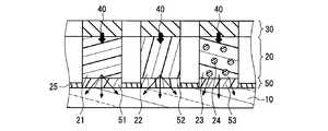
本実施形態の多色発光装置は、図1に示すように、透光性基板10上に、遮光層25と、色変換部材20と発光部材30から構成される。色変換部材20は、蛍光体層である緑色蛍光体層21および赤色蛍光体層22および非蛍光体層である非蛍光体層23から構成され、色変換部材2を構成する各層は、遮光層25によって遮光されていない上に配設される。発光部材30は、色変換部材20を構成する各層に対応した位置に配設される。非蛍光体層23には、非蛍光体層23と屈折率の異なる光拡散材24が分散されている。なお、遮光層25は必ずしも必要ではないが、配置した方がコントラストを向上できる。また、図1においては、色変換部材20は2つの蛍光体層と1つの非蛍光体層から構成されているが、蛍光体層と非蛍光体層はそれぞれ一つ以上あればその数は限定されるものではない。
[First embodiment]
1. Configuration of Multicolor Light Emitting Device As shown in FIG. 1, the multicolor light emitting device of this embodiment includes a
上記の構成により、蛍光体層である緑色蛍光体層21および赤色蛍光体層22において発光部材30からの発光40は吸収され、それぞれ緑色、赤色の無指向性の蛍光を発し、非蛍光体層23においては、光拡散材24により発光部材30からの発光60は拡散され指向性が無くなる。そのため、色変換部材20を形成する各層から取り出される光はすべて無指向性の光であるため、視野角特性が向上した多色発光装置となる。
With the above configuration, the
対比として、非蛍光体層に拡散材を入れない場合の発光を図4に示す。この場合は、蛍光層21および22からの光は無指向性であるが、非蛍光層23からの光は発光部材30からの光6の指向性を維持するので、各層から取り出される光の指向性が異なり、視野角特性が悪い。
For comparison, FIG. 4 shows light emission when no diffusion material is put in the non-phosphor layer. In this case, the light from the
2、各構成要素について
(1)透光性基板
本発明で用いられる透光性基板は、多色発光装置を支持する基板であり、400nm〜700nmの可視域の光の透過率が50%以上で、平滑な基板が望ましい。具体的にはガラス板、ポリマー板などが挙げられる。
2. About each component (1) Translucent substrate The translucent substrate used by this invention is a board | substrate which supports a multicolor light-emitting device, and the transmittance | permeability of the light of the visible region of 400 nm-700 nm is 50% or more. A smooth substrate is desirable. Specifically, a glass plate, a polymer plate, etc. are mentioned.
(2)色変換部材
本発明に用いられる色変換部材は、一以上の蛍光体層と一以上の非蛍光体層から構成される。
(2) Color Conversion Member The color conversion member used in the present invention is composed of one or more phosphor layers and one or more non-phosphor layers.
蛍光体層としては、例えば蛍光色素もしくは蛍光顔料などの蛍光体、もしくは前記蛍光体をバインダー樹脂中に分散させたものが用いられる。緑色の蛍光を発する蛍光色素の例としては、3−(2’−ベンゾチアゾリル)−7−N,N−ジエチルアミノクマリン(クマリン540)などのクマリン系色素、ソルベントイエロー11などのナフタルイミド系染料が挙げられる。赤色の蛍光を発する蛍光色素の例としては、ローダミン6Gなどのローダミン系色素、4−ジシアノメチレン−2−メチル−6−(p−ジメチルアミノスチルリル)−4H−ピラン(DCM)などのシアニン系色素などが上げられる。蛍光顔料の例としては、蛍光染料をベンゾグアナミン樹脂などに練り込んで顔料化した有機蛍光顔料、もしくはSrGa2S4:EuやCaS:Euなどの無機蛍光顔料が挙げられる。これらの蛍光体は、必要に応じて単独または混合して用いてよい。 As the phosphor layer, for example, a phosphor such as a fluorescent dye or a fluorescent pigment, or a material obtained by dispersing the phosphor in a binder resin is used. Examples of fluorescent dyes that emit green fluorescence include coumarin dyes such as 3- (2′-benzothiazolyl) -7-N, N-diethylaminocoumarin (coumarin 540) and naphthalimide dyes such as Solvent Yellow 11. It is done. Examples of fluorescent dyes that emit red fluorescence include rhodamine dyes such as rhodamine 6G and cyanine dyes such as 4-dicyanomethylene-2-methyl-6- (p-dimethylaminostyryl) -4H-pyran (DCM). Pigments are raised. Examples of the fluorescent pigment include an organic fluorescent pigment obtained by kneading a fluorescent dye into a benzoguanamine resin or the like, or an inorganic fluorescent pigment such as SrGa 2 S 4 : Eu or CaS: Eu. These phosphors may be used alone or as a mixture as required.
蛍光体層のバインダー樹脂としては、透明な(可視光透過率50%以上)の材料が好ましい。例えば、ポリメチルメタクリレート(PMMA)、ポリビニルアルコール(PVA)などが挙げられる。また、蛍光体層を平面的に分離配置するためにフォトリソグラフィー法が適用できる感光性樹脂も選ばれる。例えば、アクリル酸系、メタクリル酸系などの反応性ビニル基を有する光硬化性レジスト材料が挙げられる。 The binder resin for the phosphor layer is preferably a transparent material (visible light transmittance of 50% or more). Examples thereof include polymethyl methacrylate (PMMA) and polyvinyl alcohol (PVA). In addition, a photosensitive resin to which a photolithography method can be applied in order to separate and arrange the phosphor layers in a plane is also selected. For example, a photocurable resist material having a reactive vinyl group such as acrylic acid or methacrylic acid may be used.
蛍光体層が主に蛍光体からなる場合は、所望の蛍光体層パターンのマスクを介して真空蒸着またはスパッタリング法で成膜され、一方、蛍光体とバインダー樹脂からなる場合は、蛍光体と樹脂と適当な溶剤を混合、分散または可溶化させて液状とし、スピンコート法などで成膜し、フォトリソグラフィー法で所望の蛍光体層パターンでパターニングしたり、スクリーン印刷等の方法で所望の蛍光体層パターンでパターニングするのが一般的である。 When the phosphor layer is mainly composed of a phosphor, it is formed by vacuum deposition or sputtering through a mask having a desired phosphor layer pattern. On the other hand, when the phosphor layer is composed of a phosphor and a binder resin, the phosphor and the resin are formed. And a suitable solvent are mixed, dispersed or solubilized to form a liquid, formed into a film by spin coating, etc., patterned with a desired phosphor layer pattern by photolithography, or desired phosphor by a method such as screen printing. It is common to pattern with a layer pattern.
非蛍光体層は、透光性媒体層、もしくはカラーフィルタ層が選択される。透光性媒体層は、透明(可視光透過率50%以上)であれば固体、液体、気体を問わない。固体であれば、透光性樹脂や透光性無機化合物などが挙げられる。液体の場合はシリコーンオイル等が挙げられ、気体の場合は大気、窒素ガス、不活性ガスなどが挙げられる。透光性媒体層は、蛍光体層と同様の方法でパターニングすることも可能であり、透光性基板と発光部材の間に充填することも可能である。また、透光性媒体は、単層でも良いし多層でも良い。 As the non-phosphor layer, a translucent medium layer or a color filter layer is selected. The translucent medium layer may be solid, liquid, or gas as long as it is transparent (visible light transmittance of 50% or more). If it is solid, translucent resin, translucent inorganic compound, etc. are mentioned. In the case of a liquid, silicone oil or the like can be used. In the case of a gas, air, nitrogen gas, inert gas, or the like can be used. The translucent medium layer can be patterned by the same method as the phosphor layer, and can be filled between the translucent substrate and the light emitting member. Further, the translucent medium may be a single layer or a multilayer.
カラーフィルタ層は、色素のみ、もしくは色素をバインダー樹脂中に分散させたものが用いられる。青色色素としては、銅フタロシアニン系顔料やインダンスロン系顔料などが挙げられる。緑色色素としては、ハロゲン多置換フタロシアニン系顔料などが挙げられる。赤色色素としては、ペリレン系顔料、レーキ顔料などが挙げられる。各色の色素は二種類以上使用しても良い。バインダー樹脂は蛍光体層と同様の材料を選ぶことが出来る。パターニングも蛍光体層と同様の方法を選択できる。 As the color filter layer, only a pigment or a pigment dispersed in a binder resin is used. Examples of blue pigments include copper phthalocyanine pigments and indanthrone pigments. Examples of the green colorant include halogen polysubstituted phthalocyanine pigments. Examples of red pigments include perylene pigments and lake pigments. Two or more dyes of each color may be used. As the binder resin, the same material as that of the phosphor layer can be selected. For patterning, the same method as for the phosphor layer can be selected.
光拡散材は、非蛍光体層と屈折率を異にするものが選ばれる。ここでいう非蛍光体層の屈折率とは、非蛍光体層が透光性媒体層であれば透光性媒体の屈折率、非蛍光体層がカラーフィルタ層であり色素のみで構成されている場合は色素の屈折率、非蛍光体層がカラーフィルタ層であり色素をバインダー樹脂中に分散したものであればバインダー樹脂の屈折率である。拡散材は、無機系微粒子、ポリマー微粒子から選ばれ、拡散材の粒子径は0.3〜10μmが望ましい。無機系微粒子としては、二酸化ケイ素、酸化亜鉛、酸化チタン、硫酸バリウムなどが挙げられ、ポリマー微粒子としてはポリスチレン、ベンゾグアナミン樹脂などが挙げられる。屈折率差は0.1以上が好ましい。上記の拡散材は単独で用いても良いし、ブレンドしても良い。 As the light diffusing material, a material having a refractive index different from that of the non-phosphor layer is selected. The refractive index of the non-phosphor layer here is the refractive index of the translucent medium if the non-phosphor layer is a translucent medium layer, and the non-phosphor layer is a color filter layer and is composed of only a dye. If the non-phosphor layer is a color filter layer and the dye is dispersed in the binder resin, the refractive index of the binder resin is used. The diffusing material is selected from inorganic fine particles and polymer fine particles, and the particle size of the diffusing material is preferably 0.3 to 10 μm. Examples of the inorganic fine particles include silicon dioxide, zinc oxide, titanium oxide, and barium sulfate. Examples of the polymer fine particles include polystyrene and benzoguanamine resin. The difference in refractive index is preferably 0.1 or more. The above diffusing materials may be used alone or in a blend.
(3)遮光層
遮光層はコントラスト向上のために設けられる。遮光層は、金属もしくは黒色色素、もしくは前記金属もしくは前記黒色色素をバインダー樹脂中に分散させたものが用いられる。金属の例としては、Ag、Cu、Ti、ステンレスなどの一種以上の金属もしくは合金が挙げられる。また上記金属の酸化物、硫化物、硝酸塩等を用いても良く、必要に応じて炭素が含有されていても良い。黒色色素としては、カーボンブラック、チタンブラックなどが挙げられる。遮光層は蛍光体層同様に、スパッタリング法、フォトリソグラフィー法、スクリーン印刷法などによってパターニングされる。
(3) Light shielding layer The light shielding layer is provided to improve contrast. As the light shielding layer, a metal or black pigment, or a material in which the metal or the black pigment is dispersed in a binder resin is used. Examples of the metal include one or more metals or alloys such as Ag, Cu, Ti, and stainless steel. Moreover, the said metal oxide, sulfide, nitrate etc. may be used, and carbon may be contained as needed. Examples of black pigments include carbon black and titanium black. The light shielding layer is patterned by a sputtering method, a photolithography method, a screen printing method or the like, similarly to the phosphor layer.
(4)発光部材
本発明に用いられる発光部材としては、無機ELが薄型で面発光であり、かつ長寿命である点から好ましいが、有機EL、LED,PDPなどの光源も利用できる。
(4) Light-Emitting Member As the light-emitting member used in the present invention, an inorganic EL is preferable because it is thin, has a surface emission, and has a long lifetime, but a light source such as an organic EL, LED, or PDP can also be used.
次に本発明に用いられる無機EL素子の代表的な構成について述べる。無機EL素子は、対向する2つの電極間に少なくとも発光層を備える。前記電極の少なくとも一つは透明電極である必要があり、前記透明電極には、厚みが200〜300μmのインジウム−スズ酸化物合金(ITO)からなる透明電極層を用いる。前記発光層は、無機又は有機の蛍光体等の発光物体を層状にしたものである。前記発光層の両側又は片側には電気絶縁層(誘電体層)を配置してもよい。無機蛍光体の場合は、対向する2つの電極間に誘電体層を設け、キャパシターの原理を用いて電界により蛍光体からなる発光層を発光させる。誘電体層としては、Y2O3,Li2O,MgO,CaO,BaO,SrO,Al2O3,SiO2,MgTiO3,CaTiO3,BaTiO3,SrTiO3,ZrO2,TiO2,B2O3,PbTiO3,PbZrO3,PbZrTiO3(PZT)の少なくとも1種類を使用できる。さらに、両電極間には強誘電体層を介在させ、さらに発光効率を上げる手段を講じてもよい。 Next, a typical configuration of the inorganic EL element used in the present invention will be described. The inorganic EL element includes at least a light emitting layer between two opposing electrodes. At least one of the electrodes needs to be a transparent electrode, and a transparent electrode layer made of an indium-tin oxide alloy (ITO) having a thickness of 200 to 300 μm is used for the transparent electrode. The light emitting layer is formed by layering a light emitting object such as an inorganic or organic phosphor. An electric insulating layer (dielectric layer) may be disposed on both sides or one side of the light emitting layer. In the case of an inorganic phosphor, a dielectric layer is provided between two opposing electrodes, and a light emitting layer made of the phosphor is caused to emit light by an electric field using the principle of a capacitor. As the dielectric layer, Y 2 O 3 , Li 2 O, MgO, CaO, BaO, SrO, Al 2 O 3 , SiO 2 , MgTiO 3 , CaTiO 3 , BaTiO 3 , SrTiO 3 , ZrO 2 , TiO 2 , B At least one of 2 O 3 , PbTiO 3 , PbZrO 3 , and PbZrTiO 3 (PZT) can be used. Further, a ferroelectric layer may be interposed between both electrodes, and a means for further increasing the luminous efficiency may be taken.
発光層に使用可能な発光物質としては、例えばZnS:Ag,ZnS:Cu,ZnS:Mn,SrS:Ce:Eu,ZnS:Sm:Cl,CaS:Eu,ZnS:Tb:F,CaS:Ce,ZnMgS:Mn,CaGa2S4:Ce,SrS:Cu,CaS:Pb,BaAl2S4:Eu,Y2O3:Eu,Ca2Ge2O7:Mn等の蛍光体として一般に知られているものを用いることができる。 Examples of the light-emitting substance that can be used in the light-emitting layer include ZnS: Ag, ZnS: Cu, ZnS: Mn, SrS: Ce: Eu, ZnS: Sm: Cl, CaS: Eu, ZnS: Tb: F, and CaS: Ce. ZnMgS: Mn, CaGa 2 S 4 : Ce, SrS: Cu, CaS: Pb, BaAl 2 S 4: Eu, Y 2 O 3: Eu, Ca 2 Ge 2 O 7: generally known as a phosphor, such as Mn Can be used.
〔第二実施形態〕
本実施形態の多色発光装置を図2に示す。本実施形態は、第一実施形態に対して、非蛍光体層23が光拡散材を有していない点と、非蛍光体層23の透光性基盤10側表面が光拡散面26となっている点で異なる。第二実施形態においても、非蛍光体層から取り出される光も無指向性の光になるため、第一実施形態と同様の効果となる。
[Second Embodiment]
The multicolor light emitting device of this embodiment is shown in FIG. The present embodiment is different from the first embodiment in that the
〔第三実施形態〕
本実施形態の多色発光装置を図3に示す。本実施形態は、第二実施形態に対して、非蛍光体層23の光拡散面26が、発光部材30側に形成されている点で異なる。第三実施形態においても、発光部材からの光40が光拡散面26により無指向性になり、その結果非蛍光体層から取り出される光も無指向性の光になるため、第一実施形態と同様の効果となる。
[Third embodiment]
A multicolor light emitting device of this embodiment is shown in FIG. This embodiment is different from the second embodiment in that the
〔第四実施形態〕
本実施形態の多色発光装置を、図4に示す。本実施形態は、第一実施形態に透光性基板10と色変換部材20との間にカラーフィルタ層50が配設されたものである。図1と同一部分には同一符号を付して詳しい説明は省略する。カラーフィルタ層50は、第一実施形態の非蛍光体層にカラーフィルタ層を選択した場合と同様の材料を選択でき、同様のプロセスでパターニングできる。カラーフィルタ層50に光拡散材は添加されていてもされていなくても良い。カラーフィルタ層50により、あらゆる視野角に取り出される光の色純度を高められるため視野角特性をさらに向上できる。
[Fourth embodiment]
The multicolor light emitting device of this embodiment is shown in FIG. In the present embodiment, a
〔第五実施形態〕
本実施形態の多色発光装置を図5に示す。本実施形態は第一実施形態に対して、非蛍光体層23に光拡散材が添加されていない点と、透光性基板10と色変換部材20との間に光拡散層60が配設されている点で異なる。拡散層60は、第一実施形態の非蛍光体層および第一実施形態の光拡散材と同様の材料を選択でき、同様のプロセスでパターニングできる。光拡散層60により、各色から取り出される光は全て無指向性のため第一実施形態と同様の効果が期待でき、光拡散層60が光拡散材を含むカラーフィルタ層であれば第四実施形態と同様な理由により、より視野角特性を向上できる。
[Fifth embodiment]
The multicolor light emitting device of this embodiment is shown in FIG. The present embodiment is different from the first embodiment in that a
〔第六実施形態〕
本実施形態の多色発光装置を図6に示す。第五実施形態と比較して、光拡散層60が光拡散材を有していない点と、青色拡散層63の透光性基盤10側表面が光拡散面66となっている点で異なる。第六実施形態においても、各色から取り出される光も無指向性の光になるため、第一実施形態と同様の効果となる。
[Sixth embodiment]
The multicolor light emitting device of this embodiment is shown in FIG. Compared to the fifth embodiment, the
〔第七実施形態〕
本実施形態の多色発光装置を図7に示す。本実施形態は、第六実施形態に対して、青色拡散層63の光拡散面66が、発光部材30側に形成されている点で異なる。第三実施形態においても、発光部材からの光40が光拡散面26により無指向性になり、その結果非蛍光体層から取り出される光も無指向性の光になるため、第一実施形態と同様の効果となる。
[Seventh embodiment]
The multicolor light emitting device of this embodiment is shown in FIG. This embodiment is different from the sixth embodiment in that the
次に、本発明の効果を、具体的な実施例に基づいて説明する。 Next, the effect of this invention is demonstrated based on a specific Example.
(実施例1)
以下の仕様で色変換部材のペーストを作成した。
(1)色変換部材の形成
(1−1)蛍光体層ペーストの作成
以下の成分を90℃で20分混合し、塗材ペーストを作成した。
(a)溶媒
ベンジルアルコール:10g
(b)バインダー樹脂
ポリメチルメタクリレート粉末(PMMA:住友化学工業製、屈折率1.49):4g
(c)蛍光体
緑:クマリン540(Exciton社製):50mg
赤:DCM(Exciton社製):50mg
(1−2)非蛍光体層ペーストの作製
以下の成分を90℃で20分混合し、塗材ペーストを作成した。
(a)溶媒
ベンジルアルコール:10g
(b)透光性媒体
ポリメチルメタクリレート粉末(PMMA:住友化学工業製、屈折率1.49):4g
(c)拡散材
ベンゾグアナミン樹脂微粒子(日本触媒製 エポスターMS 屈折率1.66) 2g
ガラス基板の表面に、グラファイトとPMMAを含む厚さ2μm、幅50μm、ピッチ間隔150μmの遮光層を形成した。この遮光層の上に前記ピッチ間隔をまたいで、前記緑と赤の蛍光体層ペーストと非蛍光体層ペーストをスクリーン印刷法により緑色蛍光体層、赤色蛍光体層、非蛍光体層の順番に各々印刷した。スクリーン印刷版は400メッシュ/インチのものを使用した。印刷後溶媒を徐々に蒸発させ、170℃、60分で乾燥した。乾燥後の膜厚は15μmであった。色変換部材表面の算術平均粗さRaは0.4μmであった。
Example 1
The paste of the color conversion member was created with the following specifications.
(1) Formation of color conversion member (1-1) Preparation of phosphor layer paste The following components were mixed at 90 ° C. for 20 minutes to prepare a coating material paste.
(A) Solvent benzyl alcohol: 10 g
(B) Binder resin Polymethylmethacrylate powder (PMMA: manufactured by Sumitomo Chemical Co., Ltd., refractive index 1.49): 4 g
(C) Phosphor Green: Coumarin 540 (Exciton): 50 mg
Red: DCM (manufactured by Exciton): 50mg
(1-2) Preparation of non-phosphor layer paste The following components were mixed at 90 ° C. for 20 minutes to prepare a coating material paste.
(A) Solvent benzyl alcohol: 10 g
(B) Translucent medium Polymethylmethacrylate powder (PMMA: manufactured by Sumitomo Chemical Co., Ltd., refractive index 1.49): 4 g
(C) Diffusion material benzoguanamine resin fine particles (Nippon Shokubai Eposter MS refractive index 1.66) 2g
A light shielding layer having a thickness of 2 μm, a width of 50 μm, and a pitch interval of 150 μm containing graphite and PMMA was formed on the surface of the glass substrate. The green and red phosphor layer paste and the non-phosphor layer paste are screen-printed on the light shielding layer in the order of the green phosphor layer, the red phosphor layer, and the non-phosphor layer. Each printed. The screen printing plate used was 400 mesh / inch. After printing, the solvent was gradually evaporated and dried at 170 ° C. for 60 minutes. The film thickness after drying was 15 μm. The arithmetic average roughness Ra of the color conversion member surface was 0.4 μm.
以下図面を用いて説明する。図1は本発明の実施例1における多色発光装置の断面図である。透光性基板10の上に前記遮光層25が形成され、その上に色変換部材20を構成する緑色蛍光体層21、赤色蛍光体層22、非蛍光体層23が形成されている。その上に別プロセスにて作成された無機ELである発光部材30を色変換部材20に対応する位置に重ね合わせて多色発光装置とした。
This will be described below with reference to the drawings. FIG. 1 is a cross-sectional view of a multicolor light emitting device in Example 1 of the present invention. The
図8は本発明の一実施例において無機ELである発光部材30を示す断面図である。まず、Al2O3から成る厚み1mmの背面基板31の上に1μmの厚みの銅配線からなる背面電極32をストライプ状に平行に形成した。その上に、厚み30μmのBaTiO3からなる誘電体層33と、厚み0.6μmのBaTiO3有機酸からなる平滑層34と、その上に厚み0.6μmのBaAl2S4:Euからなる蛍光体発光層35と、厚み0.5μmのAl2O3からなる拡散防止層36を形成した。その上に厚み0.5μm、幅150μmのインジウム−スズ酸化物合金(ITO)層(屈折率n=2.1)からなる透明電極37を背面電極32と直交する方向にストライプ状に平行に形成した。
FIG. 8 is a cross-sectional view showing a
(実施例2)
蛍光体層ペーストは実施例1と同一仕様、非蛍光体層ペーストは、実施例1に対して光拡散材を含まない仕様で作成した。
(Example 2)
The phosphor layer paste was prepared with the same specifications as in Example 1, and the non-phosphor layer paste was prepared with specifications that did not include a light diffusing material with respect to Example 1.
非蛍光体層が塗布される部分の表面粗さが1.0μmである透光性基板の表面に、グラファイトとPMMAを含む厚さ2μm、幅50μm、ピッチ間隔150μmの遮光層を形成した。この遮光層の上に前記ピッチ間隔をまたいで、前記緑と赤の蛍光体層ペーストと非蛍光体層ペーストをスクリーン印刷法により緑色蛍光体層、赤色蛍光体層、非蛍光体層の順番に各々印刷した。スクリーン印刷版は400メッシュ/インチのものを使用した。印刷後溶媒を徐々に蒸発させ、170℃、60分で乾燥した。乾燥後の膜厚は15μmであった。色変換部材表面の算術平均粗さRaは0.4μmであった。 A light-shielding layer having a thickness of 2 μm, a width of 50 μm, and a pitch interval of 150 μm containing graphite and PMMA was formed on the surface of a translucent substrate having a surface roughness of 1.0 μm on the portion to which the non-phosphor layer was applied. The green and red phosphor layer paste and the non-phosphor layer paste are screen-printed on the light shielding layer in the order of the green phosphor layer, the red phosphor layer, and the non-phosphor layer. Each printed. The screen printing plate used was 400 mesh / inch. After printing, the solvent was gradually evaporated and dried at 170 ° C. for 60 minutes. The film thickness after drying was 15 μm. The arithmetic average roughness Ra of the color conversion member surface was 0.4 μm.
図2は本発明の実施例2における多色発光装置の断面図である。透光性基板10の上に前記遮光層25が形成され、その上に色変換部材20を構成する緑色蛍光体層21、赤色蛍光体層22、非蛍光体層23が形成されている。この時、非蛍光体層23の透光性基板10側の表面は、透光性基板10の粗さの影響を受けるため、光拡散面26となっている。その上に別プロセスにて作成された無機ELである発光部材30を色変換部材20に対応する位置に重ね合わせて多色発光装置とした。
FIG. 2 is a cross-sectional view of a multicolor light emitting device in Example 2 of the present invention. The
(実施例3)
色変換部材のペーストは実施例2と同一の仕様で作成した。
(Example 3)
The paste for the color conversion member was prepared with the same specifications as in Example 2.
ガラス基板の表面に、グラファイトとPMMAを含む厚さ2μm、幅50μm、ピッチ間隔150μmの遮光層を形成した。この遮光層の上に前記ピッチ間隔をまたいで、前記緑と赤の蛍光体層ペーストと非蛍光体層ペーストをスクリーン印刷法により緑色蛍光体層、赤色蛍光体層、非蛍光体層の順番に各々印刷した。この時、蛍光体層の印刷には、400メッシュ/インチのスクリーン版を使用し、非蛍光体層の印刷には、200メッシュ/インチのスクリーン版を使用した。印刷後に溶媒を徐々に蒸発させ、170℃、60分で乾燥した。乾燥後の膜厚は15μmであった。蛍光体層表面の算術平均粗さRaは0.4μmであり、非蛍光体層表面の算術平均粗さRaは1.0μmであった。 A light shielding layer having a thickness of 2 μm, a width of 50 μm, and a pitch interval of 150 μm containing graphite and PMMA was formed on the surface of the glass substrate. The green and red phosphor layer paste and the non-phosphor layer paste are screen-printed on the light shielding layer in the order of the green phosphor layer, the red phosphor layer, and the non-phosphor layer. Each printed. At this time, a 400 mesh / inch screen plate was used for printing the phosphor layer, and a 200 mesh / inch screen plate was used for printing the non-phosphor layer. After printing, the solvent was gradually evaporated and dried at 170 ° C. for 60 minutes. The film thickness after drying was 15 μm. The arithmetic average roughness Ra of the phosphor layer surface was 0.4 μm, and the arithmetic average roughness Ra of the non-phosphor layer surface was 1.0 μm.
図3は本発明の実施例2における多色発光装置の断面図である。透光性基板10の上に前記遮光層25が形成され、その上に色変換部材20を構成する緑色蛍光体層21、赤色蛍光体層22、非蛍光体層23が形成されている。その上に別プロセスにて作成された無機ELである発光部材30を色変換部材20に対応する位置に重ね合わせて多色発光装置とした。この時、非蛍光体層23の発光部材30側表面は光拡散面26となっている。
FIG. 3 is a cross-sectional view of a multicolor light emitting device in Example 2 of the present invention. The
(実施例4)
実施例1と同じ仕様で色変換部材のペーストを作成し、以下の仕様でカラーフィルタ層のペーストを作成した。
Example 4
A paste for the color conversion member was created with the same specifications as in Example 1, and a paste for the color filter layer was created with the following specifications.
(2)カラーフィルタ層ペーストの作成
以下の成分を90℃で20分混合し、塗材ペーストを作成した。
(2) Preparation of color filter layer paste The following components were mixed at 90 ° C. for 20 minutes to prepare a coating material paste.
(a)溶媒
ベンジルアルコール:10g
(b)バインダー樹脂
ポリメチルメタクリレート粉末(PMMA:住友化学工業製、屈折率1.49):4g
(c)色素
青:銅フタロシアニン系顔料(C.I.ピグメントブルー15:6)1g
緑:ハロゲン化銅フタロシアニン系顔料(C.I.ピグメントグリーン36)1g
赤:アントラキノン系顔料(C.I.ピグメントレッド177)1g
ガラス基板の表面に、グラファイトとPMMAを含む厚さ2μm、幅50μm、ピッチ間隔150μmの遮光層を形成した。この遮光層の上に前記ピッチ間隔をまたいで、前記カラーフィルタをスクリーン印刷法により、緑色フィルタ層、赤色フィルタ層、青色フィルタ層の順番で各々印刷した。スクリーン印刷版は400メッシュ/インチのものを使用した。印刷後溶媒を徐々に蒸発させ、170℃、60分で乾燥した。乾燥後のカラーフィルタ層の膜厚は3μmであった。カラーフィルタ層表面の算術平均粗さRaは0.4μmであった。その上に前記緑と赤の蛍光体層ペーストと非蛍光体層ペーストをスクリーン印刷法により、緑色蛍光体層、赤色蛍光体層、非蛍光体層の順番に各々印刷した。スクリーン印刷版は400メッシュ/インチのものを使用した。印刷後溶媒を徐々に蒸発させ、170℃、60分で乾燥した。乾燥後の膜厚は15μmであった。色変換部材表面の算術平均粗さRaは0.4μmであった。
(A) Solvent benzyl alcohol: 10 g
(B) Binder resin Polymethylmethacrylate powder (PMMA: manufactured by Sumitomo Chemical Co., Ltd., refractive index 1.49): 4 g
(C) Dye Blue: 1 g of copper phthalocyanine pigment (CI Pigment Blue 15: 6)
Green: 1 g of halogenated copper phthalocyanine pigment (CI Pigment Green 36)
Red: 1 g of anthraquinone pigment (CI Pigment Red 177)
A light shielding layer having a thickness of 2 μm, a width of 50 μm, and a pitch interval of 150 μm containing graphite and PMMA was formed on the surface of the glass substrate. The color filter was printed on the light shielding layer in the order of a green filter layer, a red filter layer, and a blue filter layer by screen printing, with the pitch interval being crossed. The screen printing plate used was 400 mesh / inch. After printing, the solvent was gradually evaporated and dried at 170 ° C. for 60 minutes. The film thickness of the color filter layer after drying was 3 μm. The arithmetic average roughness Ra of the color filter layer surface was 0.4 μm. The green and red phosphor layer paste and the non-phosphor layer paste were printed on the green phosphor layer, the red phosphor layer, and the non-phosphor layer in this order by screen printing. The screen printing plate used was 400 mesh / inch. After printing, the solvent was gradually evaporated and dried at 170 ° C. for 60 minutes. The film thickness after drying was 15 μm. The arithmetic average roughness Ra of the color conversion member surface was 0.4 μm.
図4は本発明の実施例4における多色発光装置の断面図である。透光性基板10の上に前記遮光層25が形成され、その上にカラーフィルタ層50を構成する緑色フィルタ層51、赤色フィルタ層52、青色フィルタ層53を形成され、その上に色変換部材20を構成する緑色蛍光体層21、赤色蛍光体層22、非蛍光体層23が形成されている。その上に第一実施形態と同様に別プロセスにて作成された無機ELである発光部材30を色変換部材20に対応する位置に重ね合わせて多色発光装置とした。
FIG. 4 is a cross-sectional view of a multicolor light emitting device in Example 4 of the present invention. The
(実施例5)
非蛍光体層を除いて実施例1と同じ仕様で色変換部材のペーストを作成し、以下の仕様で色変換部材の非蛍光体層および拡散層のペーストを作成した。
(3−1)非蛍光体層ペーストの作製
以下の成分を90℃で20分混合し、塗材ペーストを作成した。
(a)溶媒
ベンジルアルコール:10g
(b)透光性媒体
ポリメチルメタクリレート粉末(PMMA:住友化学工業製、屈折率1.49):4g
(3−2)拡散層
以下の成分を90℃で20分混合し、塗材ペーストを作成した。
(Example 5)
A paste for the color conversion member was prepared with the same specifications as in Example 1 except for the non-phosphor layer, and a paste for the non-phosphor layer and the diffusion layer of the color conversion member was prepared with the following specifications.
(3-1) Preparation of non-phosphor layer paste The following components were mixed at 90 ° C. for 20 minutes to prepare a coating material paste.
(A) Solvent benzyl alcohol: 10 g
(B) Translucent medium Polymethylmethacrylate powder (PMMA: manufactured by Sumitomo Chemical Co., Ltd., refractive index 1.49): 4 g
(3-2) Diffusion Layer The following components were mixed at 90 ° C. for 20 minutes to prepare a coating material paste.
(a)溶媒
ベンジルアルコール:10g
(b)バインダー樹脂
ポリメチルメタクリレート粉末(PMMA:住友化学工業製、屈折率1.49):4g
(c)色素
青:銅フタロシアニン系顔料(C.I.ピグメントブルー15:6)1g
緑:ハロゲン化銅フタロシアニン系顔料(C.I.ピグメントグリーン36)1g
赤:アントラキノン系顔料(C.I.ピグメントレッド177)1g
(d)拡散材
ベンゾグアナミン樹脂微粒子(日本触媒製 エポスターMS 屈折率1.66) 2g
ガラス基板の表面に、グラファイトとPMMAを含む厚さ2μm、幅50μm、ピッチ間隔150μmの遮光層を形成した。この遮光層の上に前記ピッチ間隔をまたいで、前記光拡散層をスクリーン印刷法により、緑色拡散層、赤色拡散層、青色拡散層の順番で各々印刷した。スクリーン印刷版は400メッシュ/インチのものを使用した。印刷後溶媒を徐々に蒸発させ、170℃、60分で乾燥した。乾燥後の光拡散層の膜厚は3μmであった。光拡散層表面の算術平均粗さRaは0.4μmであった。その上に前記緑と赤の蛍光体層ペーストと非蛍光体層ペーストをスクリーン印刷法により、緑色蛍光体層、赤色蛍光体層、非蛍光体層の順番に各々印刷した。スクリーン印刷版は400メッシュ/インチのものを使用した。印刷後溶媒を徐々に蒸発させ、170℃、60分で乾燥した。乾燥後の膜厚は15μmであった。色変換部材表面の算術平均粗さRaは0.4μmであった。
(A) Solvent benzyl alcohol: 10 g
(B) Binder resin Polymethylmethacrylate powder (PMMA: manufactured by Sumitomo Chemical Co., Ltd., refractive index 1.49): 4 g
(C) Dye Blue: 1 g of copper phthalocyanine pigment (CI Pigment Blue 15: 6)
Green: 1 g of halogenated copper phthalocyanine pigment (CI Pigment Green 36)
Red: 1 g of anthraquinone pigment (CI Pigment Red 177)
(D) Diffusion material Benzoguanamine resin fine particles (Epaster MS refractive index 1.66 made by Nippon Shokubai) 2g
A light shielding layer having a thickness of 2 μm, a width of 50 μm, and a pitch interval of 150 μm containing graphite and PMMA was formed on the surface of the glass substrate. On the light shielding layer, the light diffusion layer was printed in the order of a green diffusion layer, a red diffusion layer, and a blue diffusion layer by a screen printing method across the pitch interval. The screen printing plate used was 400 mesh / inch. After printing, the solvent was gradually evaporated and dried at 170 ° C. for 60 minutes. The thickness of the light diffusion layer after drying was 3 μm. The arithmetic average roughness Ra of the light diffusion layer surface was 0.4 μm. The green and red phosphor layer paste and the non-phosphor layer paste were printed on the green phosphor layer, the red phosphor layer, and the non-phosphor layer in this order by screen printing. The screen printing plate used was 400 mesh / inch. After printing, the solvent was gradually evaporated and dried at 170 ° C. for 60 minutes. The film thickness after drying was 15 μm. The arithmetic average roughness Ra of the color conversion member surface was 0.4 μm.
図5は本発明の実施例5における多色発光装置の断面図である。透光性基板10の上に前記遮光層25が形成され、その上に拡散層60を構成する緑色拡散層61、赤色拡散層62、青色拡散層63を形成され、その上に色変換部材20を構成する緑色蛍光体層21、赤色蛍光体層22、非蛍光体層23が形成されている。その上に第一実施形態と同様に別プロセスにて作成された無機ELである発光部材30を色変換部材20に対応する位置に重ね合わせて多色発光装置とした。
FIG. 5 is a cross-sectional view of a multicolor light emitting device in Example 5 of the present invention. The
(実施例6)
色変換部材ペーストは実施例5と同一仕様、光拡散層ペーストは、実施例5に対して光拡散材を含まない仕様で作成した。
(Example 6)
The color conversion member paste was prepared with the same specifications as in Example 5, and the light diffusion layer paste was prepared with the specifications not including the light diffusion material with respect to Example 5.
非蛍光体層が塗布される部分の表面粗さが1.0μmであるガラス基板の表面に、グラファイトとPMMAを含む厚さ2μm、幅50μm、ピッチ間隔150μmの遮光層を形成した。この遮光層の上に前記ピッチ間隔をまたいで、前記光拡散層をスクリーン印刷法により、緑色拡散層、赤色拡散層、青色拡散層の順番で各々印刷した。スクリーン印刷版は400メッシュ/インチのものを使用した。印刷後溶媒を徐々に蒸発させ、170℃、60分で乾燥した。乾燥後の光拡散層の膜厚は3μmであった。光拡散層表面の算術平均粗さRaは0.4μmであった。その上に前記緑と赤の蛍光体層ペーストと非蛍光体層ペーストをスクリーン印刷法により、緑色蛍光体層、赤色蛍光体層、非蛍光体層の順番に各々印刷した。スクリーン印刷版は400メッシュ/インチのものを使用した。印刷後溶媒を徐々に蒸発させ、170℃、60分で乾燥した。乾燥後の膜厚は15μmであった。色変換部材表面の算術平均粗さRaは0.4μmであった。 A light shielding layer having a thickness of 2 μm, a width of 50 μm, and a pitch interval of 150 μm containing graphite and PMMA was formed on the surface of a glass substrate having a surface roughness of 1.0 μm where the non-phosphor layer was applied. On the light shielding layer, the light diffusion layer was printed in the order of a green diffusion layer, a red diffusion layer, and a blue diffusion layer by a screen printing method across the pitch interval. The screen printing plate used was 400 mesh / inch. After printing, the solvent was gradually evaporated and dried at 170 ° C. for 60 minutes. The thickness of the light diffusion layer after drying was 3 μm. The arithmetic average roughness Ra of the light diffusion layer surface was 0.4 μm. The green and red phosphor layer paste and the non-phosphor layer paste were printed on the green phosphor layer, the red phosphor layer, and the non-phosphor layer in this order by screen printing. The screen printing plate used was 400 mesh / inch. After printing, the solvent was gradually evaporated and dried at 170 ° C. for 60 minutes. The film thickness after drying was 15 μm. The arithmetic average roughness Ra of the color conversion member surface was 0.4 μm.
図6は本発明の実施例6における多色発光装置の断面図である。透光性基板10の上に前記遮光層25が形成され、その上に拡散層60を構成する緑色拡散層61、赤色拡散層62、青色拡散層63を形成されている。この時、青色拡散層63の透光性基板10側界面は、ガラス基板の粗さの影響を受け光拡散面66となっている。その上に色変換部材20を構成する緑色蛍光体層21、赤色蛍光体層22、非蛍光体層23が形成されている。その上に第一実施形態と同様に別プロセスにて作成された無機ELである発光部材30を色変換部材20に対応する位置に重ね合わせて多色発光装置とした。
FIG. 6 is a cross-sectional view of a multicolor light emitting device in Example 6 of the present invention. The
(実施例7)
色変換部材ペーストおよび光拡散層ペーストは、実施例6と同一の仕様で作成した。
(Example 7)
The color conversion member paste and the light diffusion layer paste were prepared with the same specifications as in Example 6.
ガラス基板の表面に、グラファイトとPMMAを含む厚さ2μm、幅50μm、ピッチ間隔150μmの遮光層を形成した。この遮光層の上に前記ピッチ間隔をまたいで、前記光拡散層をスクリーン印刷法により、緑色拡散層、赤色拡散層、青色拡散層の順番で各々印刷した。緑色拡散層と赤色拡散層の印刷には400メッシュ/インチのものをはスクリーン印刷版を使用し、印刷後に溶媒を徐々に蒸発させ、170℃、60分で乾燥した。乾燥後の拡散層の膜厚は3μmであった。緑色および赤色拡散層表面の算術平均粗さRaは0.4μmであり、青色拡散層表面の算術平均粗さRaは1.0μmであった。その上に前記緑と赤の蛍光体層ペーストと非蛍光体層ペーストをスクリーン印刷法により、緑色蛍光体層、赤色蛍光体層、非蛍光体層の順番に各々印刷した。スクリーン印刷版は400メッシュ/インチのものを使用した。印刷後溶媒を徐々に蒸発させ、170℃、60分で乾燥した。乾燥後の膜厚は15μmであった。色変換部材表面の算術平均粗さRaは0.4μmであった。 A light shielding layer having a thickness of 2 μm, a width of 50 μm, and a pitch interval of 150 μm containing graphite and PMMA was formed on the surface of the glass substrate. On the light shielding layer, the light diffusion layer was printed in the order of a green diffusion layer, a red diffusion layer, and a blue diffusion layer by a screen printing method across the pitch interval. A screen printing plate having a mesh size of 400 mesh / inch was used for printing the green diffusion layer and the red diffusion layer. After printing, the solvent was gradually evaporated and dried at 170 ° C. for 60 minutes. The thickness of the diffusion layer after drying was 3 μm. The arithmetic average roughness Ra of the green and red diffusion layer surfaces was 0.4 μm, and the arithmetic average roughness Ra of the blue diffusion layer surfaces was 1.0 μm. The green and red phosphor layer paste and the non-phosphor layer paste were printed on the green phosphor layer, the red phosphor layer, and the non-phosphor layer in this order by screen printing. The screen printing plate used was 400 mesh / inch. After printing, the solvent was gradually evaporated and dried at 170 ° C. for 60 minutes. The film thickness after drying was 15 μm. The arithmetic average roughness Ra of the color conversion member surface was 0.4 μm.
図7は本発明の実施例7における多色発光装置の断面図である。透光性基板10の上に前記遮光層25が形成され、その上に拡散層60を構成する緑色拡散層61、赤色拡散層62、青色拡散層63を形成されている。この時、青色拡散層63の透光性基板10側界面は、ガラス基板の粗さの影響を受け光拡散面66となっている。その上に色変換部材20を構成する緑色蛍光体層21、赤色蛍光体層22、非蛍光体層23が形成されている。この時、青色拡散層63と非蛍光体層23の界面は光拡散面66となっている。その上に第一実施形態と同様に別プロセスにて作成された無機ELである発光部材30を色変換部材20に対応する位置に重ね合わせて多色発光装置とした。
FIG. 7 is a cross-sectional view of a multicolor light emitting device in Example 7 of the present invention. The
(比較例1)
実施例1の非蛍光体層に拡散材を含まない以外は、実施例1と同様の材料かつ同様のプロセスで作成した。
(Comparative Example 1)
The non-phosphor layer of Example 1 was prepared by the same material and the same process as in Example 1 except that no diffusing material was contained.
(評価)
各実施例および比較例にて作成された多色発光装置をゴニオステージに固定し、それぞれ1kHz、実効電圧200Vの交流電圧を印加して点灯状態にして、パネル法線の角度を0°とし、上下左右にそれぞれ80°まで回転させ、色度(CIE−x、y)の角度依存性を測定する。測定には、スペクトロメータ(MCPD−2000:大塚光学株式会社製)を用いた。0°の色度に対して、上下左右各々80°の範囲での色度x値およびy値の変化Δが、0.05以下であるものを良好とし、それ以外を不良と判定した。
(Evaluation)
The multicolor light emitting devices created in each of the examples and comparative examples are fixed to a gonio stage, applied with an alternating voltage of 1 kHz and an effective voltage of 200 V, respectively, and turned on, and the angle of the panel normal is set to 0 °. The angle dependency of chromaticity (CIE-x, y) is measured by rotating up, down, left and right up to 80 °. For the measurement, a spectrometer (MCPD-2000: manufactured by Otsuka Optical Co., Ltd.) was used. With respect to the chromaticity of 0 °, the change Δ of the chromaticity x value and the y value in the range of 80 ° up, down, left and right was determined to be good if it was 0.05 or less, and the others were determined to be poor.

表1から明らかなとおり、本発明の実施例はいずれも視野角特性色度変化量が小さく、視野角特性が高かった。 As is apparent from Table 1, all the examples of the present invention had a small viewing angle characteristic chromaticity change amount and a high viewing angle characteristic.
10 透光性基板
20 色変換部材
21 緑色蛍光体層
22 赤色蛍光体層
23 非蛍光体層
24 拡散材
25 遮光層
26 光拡散面
30 発光部材
31 背面基板
32 背面電極
33 誘電体層
34 平滑層
35 蛍光体発光層
36 拡散防止層
37 透明電極
40 発光部材からの光
50 カラーフィルタ層
51 緑色カラーフィルタ層
52 赤色カラーフィルタ層
53 青色カラーフィルタ層
60 拡散層
61 緑色拡散層
62 赤色拡散層
63 青色拡散層
66 光拡散面
DESCRIPTION OF
Claims (7)
The multicolor light-emitting device according to claim 5, wherein the non-phosphor layer has light diffusivity when at least one surface of the light diffusion layer is a light diffusion surface having an arithmetic average roughness of 1.0 μm or more.
Priority Applications (1)
| Application Number | Priority Date | Filing Date | Title |
|---|---|---|---|
| JP2005044272A JP2006228677A (en) | 2005-02-21 | 2005-02-21 | Polychromatic light emitting device |
Applications Claiming Priority (1)
| Application Number | Priority Date | Filing Date | Title |
|---|---|---|---|
| JP2005044272A JP2006228677A (en) | 2005-02-21 | 2005-02-21 | Polychromatic light emitting device |
Publications (1)
| Publication Number | Publication Date |
|---|---|
| JP2006228677A true JP2006228677A (en) | 2006-08-31 |
Family
ID=36989845
Family Applications (1)
| Application Number | Title | Priority Date | Filing Date |
|---|---|---|---|
| JP2005044272A Withdrawn JP2006228677A (en) | 2005-02-21 | 2005-02-21 | Polychromatic light emitting device |
Country Status (1)
| Country | Link |
|---|---|
| JP (1) | JP2006228677A (en) |
Cited By (8)
| Publication number | Priority date | Publication date | Assignee | Title |
|---|---|---|---|---|
| JP2007073219A (en) * | 2005-09-05 | 2007-03-22 | Seiko Epson Corp | Organic electroluminescent device, method of manufacturing organic electroluminescent device, and electronic apparatus |
| JP2011068123A (en) * | 2009-08-31 | 2011-04-07 | Shinsei:Kk | Molding |
| WO2012144426A1 (en) * | 2011-04-19 | 2012-10-26 | シャープ株式会社 | Fluorescent light body substrate and display device |
| WO2013039072A1 (en) * | 2011-09-16 | 2013-03-21 | シャープ株式会社 | Light-emitting device, display apparatus, illumination apparatus, and electricity-generating apparatus |
| WO2013183751A1 (en) * | 2012-06-07 | 2013-12-12 | シャープ株式会社 | Fluorescent substrate, light-emitting device, display device, and lighting device |
| CN103594482A (en) * | 2012-08-14 | 2014-02-19 | 三星显示有限公司 | Organic light emitting display device |
| WO2014084012A1 (en) * | 2012-11-30 | 2014-06-05 | シャープ株式会社 | Scatterer substrate |
| JP2019040179A (en) * | 2017-08-24 | 2019-03-14 | Jsr株式会社 | Laminate and display including laminate |
-
2005
- 2005-02-21 JP JP2005044272A patent/JP2006228677A/en not_active Withdrawn
Cited By (9)
| Publication number | Priority date | Publication date | Assignee | Title |
|---|---|---|---|---|
| JP2007073219A (en) * | 2005-09-05 | 2007-03-22 | Seiko Epson Corp | Organic electroluminescent device, method of manufacturing organic electroluminescent device, and electronic apparatus |
| JP2011068123A (en) * | 2009-08-31 | 2011-04-07 | Shinsei:Kk | Molding |
| WO2012144426A1 (en) * | 2011-04-19 | 2012-10-26 | シャープ株式会社 | Fluorescent light body substrate and display device |
| WO2013039072A1 (en) * | 2011-09-16 | 2013-03-21 | シャープ株式会社 | Light-emitting device, display apparatus, illumination apparatus, and electricity-generating apparatus |
| WO2013183751A1 (en) * | 2012-06-07 | 2013-12-12 | シャープ株式会社 | Fluorescent substrate, light-emitting device, display device, and lighting device |
| CN103594482A (en) * | 2012-08-14 | 2014-02-19 | 三星显示有限公司 | Organic light emitting display device |
| CN103594482B (en) * | 2012-08-14 | 2018-09-21 | 三星显示有限公司 | Oganic light-emitting display device |
| WO2014084012A1 (en) * | 2012-11-30 | 2014-06-05 | シャープ株式会社 | Scatterer substrate |
| JP2019040179A (en) * | 2017-08-24 | 2019-03-14 | Jsr株式会社 | Laminate and display including laminate |
Similar Documents
| Publication | Publication Date | Title |
|---|---|---|
| US20150171372A1 (en) | Fluorescent material, fluorescent coating material, phosphor substrate, electronic apparatus, and led package | |
| KR100529450B1 (en) | Organic electroluminescent display device | |
| JP5195755B2 (en) | Translucent substrate, manufacturing method thereof, organic LED element and manufacturing method thereof | |
| JP2006228677A (en) | Polychromatic light emitting device | |
| WO2013021941A1 (en) | Phosphor substrate, display device, and electronic device | |
| WO2015190594A1 (en) | Photosensitive resin composition, wavelength conversion substrate and light emitting device | |
| CN106409876A (en) | Display device | |
| KR20090024191A (en) | Color conversion substrate and color display | |
| EP3037853A1 (en) | Colour filter, colour filter array and organic light-emitting display device using the same | |
| WO2012063864A1 (en) | Light emitting element and display device | |
| JP2006269226A (en) | Color conversion filter and color conversion light emitting device using it | |
| JP2017161604A (en) | Wavelength conversion substrate, method for manufacturing wavelength conversion substrate, and display | |
| KR20060024545A (en) | High-luminance organic light-emitting device displays | |
| JP5520327B2 (en) | Color filter substrate and organic light emitting display device using the color filter substrate | |
| JP2007250547A (en) | Phosphor paste composition, plasma display panel using this, and its manufacturing method | |
| US7271536B2 (en) | Organic EL panel | |
| CN112631023B (en) | Quantum dot display panel and quantum dot display device | |
| US20060188794A1 (en) | Color conversion film and multicolor light-emitting device provided with the same | |
| JP2006303030A (en) | Electroluminescent element | |
| JP2006040642A (en) | Color conversion film and electroluminescent element using this | |
| KR100745343B1 (en) | Green color filter and organic light-emitting display device | |
| JP2006269227A (en) | Multicolor light emitting device and its manufacturing method | |
| JP2000277259A (en) | El lamp and el lamp unit using the same | |
| KR100207588B1 (en) | Electroluminescence element and manufacturing method | |
| JP2002117976A (en) | Color changing filter substrate and organic multi-color luminescent element |
Legal Events
| Date | Code | Title | Description |
|---|---|---|---|
| A300 | Application deemed to be withdrawn because no request for examination was validly filed |
Free format text: JAPANESE INTERMEDIATE CODE: A300 Effective date: 20080513 |