JP2006203579A - Tuner, method of reducing tuner interference wave and electronic apparatus - Google Patents
Tuner, method of reducing tuner interference wave and electronic apparatus Download PDFInfo
- Publication number
- JP2006203579A JP2006203579A JP2005013304A JP2005013304A JP2006203579A JP 2006203579 A JP2006203579 A JP 2006203579A JP 2005013304 A JP2005013304 A JP 2005013304A JP 2005013304 A JP2005013304 A JP 2005013304A JP 2006203579 A JP2006203579 A JP 2006203579A
- Authority
- JP
- Japan
- Prior art keywords
- tuner
- antenna
- board
- output terminal
- circuit
- Prior art date
- Legal status (The legal status is an assumption and is not a legal conclusion. Google has not performed a legal analysis and makes no representation as to the accuracy of the status listed.)
- Pending
Links
Images


Abstract
Description
本発明は、アンテナからの受信信号を受信し、チューナを介してアンテナ信号をVTR等に送出するチューナ及び妨害波低減方法並びに電子機器に係わり、特に、アンテナ受信信号がチューナのアンテナ出力端子近傍を経由する際に生ずる妨害波を減衰或いは遮断するようにしたチューナ及び妨害波低減方法並びに電子機器に関するものである。 The present invention relates to a tuner that receives a received signal from an antenna and sends the antenna signal to a VTR or the like via a tuner, a method for reducing interference waves, and an electronic device. In particular, the received antenna signal is located near the antenna output terminal of the tuner. The present invention relates to a tuner, an interference wave reducing method, and an electronic device which attenuate or block an interference wave generated when passing through.
従来から、人体が携帯無線機のアンテナに影響を与え、無線周波数の電波を吸収および散乱させ、人体が携帯無線機に近接することによって、そのアンテナのインピーダンスを変動させることを防止するため、アンテナのインピーダンスを最適値となるように予め設定しても、通話時にユーザの頭部が携帯無線機に近接することによって、アンテナのインピーダンスが最適値からシフトしてしまうという問題に対処するために、アンテナに可変リアクタンス回路を接続し、これによってアンテナのインピーダンスを調節して、送信波を歪ませることなくアンテナのインピーダンス特性を微調整することができる携帯無線機が特許文献1に開示されている。
In order to prevent the human body from affecting the antenna of the portable wireless device, absorbing and scattering radio frequency radio waves, and causing the human body to approach the portable wireless device to change the impedance of the antenna, In order to cope with the problem that the impedance of the antenna shifts from the optimal value when the user's head is close to the portable wireless device during a call even if the impedance is set to the optimal value in advance,
図4(A)は、特許文献1に開示された携帯無線機10の模式図である。携帯無線機10は、筐体1、受信アンテナ2、送信アンテナ3、受信回路4、送信回路5、可変リアクタンス回路6及び制御回路30を備えている。携帯無線機10は、時分割多重(TDM:Time Division Multiplex)によって信号の送受信を行う。
FIG. 4A is a schematic diagram of the portable wireless device 10 disclosed in
受信アンテナ2、送信アンテナ3および可変リアクタンス回路6は筐体1の外側の表面に配置されていて、送受信アンテナ2、3の少なくとも一部が筐体1の表面に固定(または半固定)されている。受信回路4、送信回路5及び制御回路30は、筐体1に内蔵されている。
The receiving
筐体1は送受信された信号が伝播する導体から成る。例えば、筐体1は金属などの導電又はプラスチックの表面に鍍金して形成されたか筐体或いは金属などの導電体から成る板状の地板である。地板の場合には、受信回路4、送信回路5、制御回路7は地板の表面に配置される。
The
信号を受信するために用いられる受信アンテナ2及び信号を送信するために用いられる送信アンテナ3は互いに分離されている。この場合、受信アンテナ2はモノポールアンテナである。受信アンテナ2は可変リアクタンス回路6に接続されており、可変リアクタンス回路6は給電点7において筐体1に接続され、送信アンテナ3は筐体1に接続されている。
A receiving
筐体1は、受信アンテナ2と接続することによって、受信波および送信波と共振するように設計される。受信回路4は、受信アンテナ2に接続され、受信アンテナ2を介して信号を受信する。送信回路5は、送信アンテナ3に接続され、送信アンテナ3を介して信号を送信する。
The
制御回路30は、受信回路4、送信回路5及び可変リアクタンス回路6に接続され、受信された信号または送信する信号に基づいて可変リアクタンス回路6を制御する。図5(B)は可変リアクタンス回路6の具体例を示す回路図である。この可変リアクタンス回路6は、ダイオードCD、インダクタンスL1及びL2、コンデンサC1、C2を有する。端子EAは受信アンテナ2に接続され、端子EBは受信回路4に接続され、端子ECはグランドに接続され、端子EDは制御回路7に接続されている。即ち、可変リアクタンス回路6の端子ECを介して受信アンテナ2が接地電位に接続した回路構成が示されている。
The
又、特許文献2にはアンテナの同軸コードの外側導体が接地線を介してセツトの基準グランドに接続するアンテナ装置が開示されている。この構成を図5で説明する。図5に於いて、8は車内アンテナを示し、同軸コード9の他端のミニプラグ11Pと、テレビジョン用のチューナ12に設けられたミニジャック11Jとを接続することにより、アンテナ8とチューナ12とが接続され、このチューナ12に接続されたテレビジョンモニタ13に所望の映像を映出する。
又、アンテナ8の給電部に格納された印刷配線基板13には、適宜のコイルL3、L4及びコンデンサC3、C4からなる回路網と、変成器構成のバルン14とが搭載されており、このバルン14の第1のコイルL5を通じて、一方のアンテナ素子16の基部16bと同軸コード9の内側導体9aとが接続されると共に、他方のアンテナ素子17の基部17bと同軸コードの外側導体9bとは、コイL4とバルン14の第4のコイルL8とを通じて接続される。
The printed
又、アンテナ素子16、17の基部16b,17bの間にコイルL3が接続され、コイルL4に並列にコンデンサC3が接続され、コンデンサC4は、バルン14の第1のコイルL5の入力側端と基板13のグラウンドパターンGpとの間に接続される。このグラウンドパターン(車体)Gpには、同軸コード9の外側導体9bも接続される。
A coil L3 is connected between the
そして、バルン13の第1のコイルL5の出力側端と第2のコイルL6の出力側端とが接続され、第4のコイルL8の出力側端と第3のコイルL7の出力側端とが接続されると共に、第2のコイルL6の入力側端と第3のコイルL7の入力側端とが接続される。
The output side end of the first coil L5 of the
なお、図5に示すように、ミニジャック11Jの一方の端子は基準電位点(グラウンドパターン)としての車体Gbに接続されるが、この基準電位点は、車の内装を一時的にも剥がさなくて良いように、例えば、ダッシュボードの下部等に、ねじ締めの形で設けられる。
As shown in FIG. 5, one terminal of the
又、グラウンド線18の一端が、例えば、ねじ止めによって、基板13のグラウンドパターンGpに接続されると共に、同軸コード14の外側導体14bの一端と接続される。
Further, one end of the
又、グラウンド線18の他端は、例えば、チューナ12のミニジャック11Jと共通に、ねじ止めによって、グラウンドとしての車体Gbに接続される。
The other end of the
上述のような形態のアンテナ装置でグラウンド線18の接続により、基板14のグラウンドパターンGpと、同軸コード9の外側導体9bの一端とが、車体Gbの基準電位とほぼ同電位になって、基板14とチューナ12での、高周波的に浮いている(フローティング)状態が解消されて不要輻射が低減される。
By connecting the
このフローティング状態の解消により、アンテナ素子16、17及び給電部をリアガラスに取り付けた場合にも、車載のテレビジョン受信機からの不要輻射に起因して、リアガラスに既設のAMアンテナに誘起されるノイズレベルを、実用上問題にならない程度まで低減することが出来るようにしている。
Due to the elimination of the floating state, even when the
上記特許文献1にはアンテナの送受信回路の接地側をグランドに接地する回路構成が記載されているが、この発明ではアンテナに可変リアクタンス回路を接続し、これによってアンテナのインピーダンスを調節して、送信波を歪ませることなくアンテナのインピーダンス特性を微調整するものである。
又、特許文献2はアンテナの同軸コードの外側導体がグランド線18を介してテレビジョン用の基準グランドに接続するアンテナ装置が開示されているが、この発明においても車載テレビジョン用の車内アンテナを車両のリアガラスに取り付けた場合の不要輻射に起因して、リアガラスに既設のAMアンテナに誘起されるノイズレベルを低減する様にしたアンテナ装置としたものである。
即ち、上記特許文献1及び特許文献2に於いては、受信アンテナ2は可変リアクタンス回路を介し接地電位に落とす構成やアンテナ同軸コードの外側導線がグランド線を介して車両のボデー(基準のグラウンドパターン(車体)Gp)に接地する構成が示されている、これに対し、本発明のチューナ及び妨害波低減方法並びに電子機器ではチューナのアンテナ出力端子近傍で生ずる妨害波がアンテナ出力回路の後段に接続したVTR等の回路に与える影響を低減或いは遮断しようとするものである。
That is, in
従来のチューナ装置では、図6に示すように、アンテナ入力端子23からの受信信号はチューナ12のチューナ基板20に配設されたRF回路やIF回路を通して所定の周波数に変換されて映像信号などに成されてLCDなどに表示される。又、アンテナ入力端子23からの受信信号はVTR等にフイルタ回路21を介し直接的にアンテナ出力端子22に出力されている。この様なチューナ12ではチューナ基板20の接地端子は接地電位のGNDに接地されている。然し、この構成では接地電位のGNDから矢印Aで示す様な妨害波24がアンテナ出力端子22に重畳されアンテナ出力端子22の後段に接続されるVTR32等の回路にノイズを与える課題があった。
In the conventional tuner device, as shown in FIG. 6, the received signal from the
本発明は上記の課題を解決するために成されたもので、本発明が解決しようとする課題は、チューナの出力端子からの妨害波の不要輻射ノイズを低減すると共にアンテナ部の強度アップを図り、アンテナの伝送経路のVSWR(電圧定在波比)を安定化させたチューナ及び妨害波低減方法並びに電子機器を得ることを目的とするものである。 The present invention has been made to solve the above-described problems. The problem to be solved by the present invention is to reduce unnecessary radiation noise of interference waves from the output terminal of the tuner and increase the strength of the antenna unit. An object of the present invention is to obtain a tuner, an interference wave reduction method, and an electronic device in which a VSWR (voltage standing wave ratio) of an antenna transmission path is stabilized.
第1の本発明は、アンテナからの受信信号をチューナシールドケース内のチューナ基板を介して受信し、チューナ基板のアンテナの出力端子よりアンテナ信号を送出する様にしたチューナに於いて、チューナ基板のアンテナの出力端子の接地電位をチューナシールドケースの接地電位と同じに成るように接続したことを特徴とするチューナとしたものである。 According to a first aspect of the present invention, there is provided a tuner configured to receive a reception signal from an antenna via a tuner board in a tuner shield case and to transmit an antenna signal from an antenna output terminal of the tuner board. The tuner is characterized in that the ground potential of the output terminal of the antenna is connected to be the same as the ground potential of the tuner shield case.
第2の本発明は、アンテナからの受信信号をチューナシールドケース内のチューナ基板を介して受信し、チューナ基板のアンテナの出力端子よりアンテナ信号を送出する様にしたチューナの妨害波低減方法に於いて、チューナ基板のアンテナの出力端子の接地電位をチューナシールドケースの接地電位と同じに成るように接続したことを特徴とするチューナの妨害波低減方法としたものである。 According to a second aspect of the present invention, there is provided a method for reducing interference of a tuner, wherein a received signal from an antenna is received via a tuner board in a tuner shield case and an antenna signal is transmitted from an antenna output terminal of the tuner board. The tuner has a method of reducing the interference wave, characterized in that the ground potential of the output terminal of the antenna of the tuner board is connected to be equal to the ground potential of the tuner shield case.
第3の本発明は、アンテナからの受信信号をチューナシールドケース内のチューナ基板を介して受信し、チューナ基板のアンテナの出力端子よりアンテナ信号を送出する様にしたチューナを有する電子機器に於いて、チューナ基板のアンテナの出力端子の接地電位をチューナシールドケースの接地電位と同じに成るように接続したことを特徴とする電子機器としたものである。 According to a third aspect of the present invention, there is provided an electronic apparatus having a tuner configured to receive a reception signal from an antenna through a tuner board in a tuner shield case and to transmit an antenna signal from an antenna output terminal of the tuner board. The electronic device is characterized in that the ground potential of the output terminal of the antenna of the tuner board is connected to be the same as the ground potential of the tuner shield case.
第1乃至第3の本発明によれば、アンテナ出力端子から導出される妨害波の不要輻射を低減することが出来ると共に伝送線路のVSWRの安定化を図ることが可能なチューナ及び妨害波低減方法並びに電子機器が得られる効果を生ずる。 According to the first to third aspects of the present invention, a tuner and an interference wave reducing method that can reduce unwanted radiation of an interference wave derived from an antenna output terminal and can stabilize the VSWR of a transmission line. In addition, an effect that an electronic device can be obtained is produced.
以下、本発明のチューナの1形態例を説明する。図1乃至図3に於いて、図1は本発明のチューナ及び妨害波低減方法を説明するための系統図、図2は図1のシールドケースの配線状態を示す要部の断面図、図3は本発明の要部の機能的系統図である。以下、図1乃至図3に於いて、図6で説明した構成との対応部分には同一符号を付して説明する。 Hereinafter, one embodiment of the tuner of the present invention will be described. 1 to 3, FIG. 1 is a system diagram for explaining the tuner and the interference wave reducing method of the present invention, FIG. 2 is a cross-sectional view of the main part showing the wiring state of the shield case of FIG. These are the functional systematic diagrams of the principal part of this invention. In the following, in FIG. 1 to FIG. 3, the same reference numerals are given to the portions corresponding to the configuration described in FIG.
以下、本発明のチューナ及び妨害波低減方法並びに電子機器を図1乃及び図2の実施の形態例で説明する。本発明の特徴とするところは、チューナのアンテナ出力端子近傍に重畳される妨害波による被りを抑制し、ノイズを低減することが出来るものを得ようとするものである。 Hereinafter, a tuner, an interference wave reducing method, and an electronic device according to the present invention will be described with reference to FIG. 1 and FIG. A feature of the present invention is to obtain a device capable of suppressing noise caused by an interference wave superimposed in the vicinity of an antenna output terminal of a tuner and reducing noise.
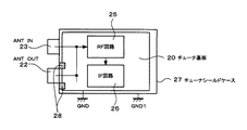
図1に於いて、20はチューナ基板であり、この基板内にはRF回路24、IF回路26等がIC化されている。IC化されたRF回路24、IF回路26等はチューナ基板20に搭載される。この場合、チューナ基板20にパターニングされる印刷配線には図2に示す様にGNDに接地する接地ライン33が設けられている。
In FIG. 1, reference numeral 20 denotes a tuner board, and an RF circuit 24, an IF
チューナ基板20は金属製のチューナシールドケース27内にビス等で固定されている。このチューナシールドケース27は略箱型に形成され、その右側面にはアンテナからの受信信号が供給される接栓座からなるアンテナ入力端子23及びアンテナからの受信信号を送信する接栓座からなるアンテナ出力端子22が固定されている。
The tuner board 20 is fixed in a metal
アンテナ入力端子23からのアンテナ受信信号(ANTIN)はRF回路25で高周波増幅され、IF回路26などで中間周波数に変換された後、所定チューニング信号がチューナ基板20の出力回路から取り出される。一方、アンテナ入力端子23から供給された受信信号は分配器(図示せず)等のフイルタ回路(図3、6参照)21を介して直接的或いはチューニングされた所定のチャンネル周波数がアンテナ出力端子22からVTR等に供給される。
An antenna reception signal (ANTIN) from the
上述した様にアンテナ受信信号をアンテナ出力端子22近傍からVTR等に供給する際にチューナ基板20の接地ライン33を介してGNDに接地した接地点を通して妨害波24がVTR32に混入する。この為、本発明では図に示す様にチューナ基板20の接地ライン33とチューナシールドケース27と半田付28により一体化させると共にチューナ基板20のGNDとチューナシールドケース27のGND1とを一体化する。
As described above, when the antenna reception signal is supplied from the vicinity of the
本発明では図3の模式図に示す様にチューナシールドケース27のGND1とチューナ基板20のGNDが同電位となるためチューナ基盤20のGNDに存在する妨害波を抑制し、アンテナ出力端子22に誘起されるノイズレベルを低減することができる。
In the present invention, as shown in the schematic diagram of FIG. 3, the
又、チューナ基板20からの輻射が低減されると共にチューナ基部20を含むアンテナ部を強固にチューナシールドケース27に固定出来てアンテナの強度アップを図ることが出来る。
In addition, radiation from the tuner board 20 can be reduced, and the antenna portion including the tuner base 20 can be firmly fixed to the
更に、チューナ基板20のGNDがより接地電位に近づく為アンテナを含む伝送経路のVSWRを安定化することが可能となる。更に又、チューナシールドケース27とチューナ基板20の接着力が増す為に長期に亘って信頼性を保持可能となる等の効果を有する。
Furthermore, since the GND of the tuner board 20 is closer to the ground potential, the VSWR of the transmission path including the antenna can be stabilized. In addition, since the adhesive force between the
尚、上述の回路構成では、チューナについて説明したが、チューナを有する各種の映像、音声信号の受信装置或いは送受信装置、テープ或いはデイスク記録再生装置、携帯電話機、PDA等の電子機器に適用可能である。 In the above circuit configuration, the tuner has been described. However, the present invention can be applied to various video and audio signal receiving devices or transmitting / receiving devices, tape or disk recording / playback devices, mobile phones, PDAs, and the like having the tuner. .
12…チューナ、20…チューナ基板、21…フイルタ回路、22…アンテナ出力端子、 23…アンテナ入力端子、 25…RF回路、 26…IF回路、 27…チューナシールドケース、 32…VTR、 33…接地ライン、GND、GND1…接地
DESCRIPTION OF
Claims (5)
前記チューナ基板のアンテナの出力端子の接地電位を前記チューナシールドケースの接地電位と同じに成るように接続したことを特徴とするチューナ。 In a tuner that receives a reception signal from an antenna via a tuner board in a tuner shield case and sends out the antenna signal from an output terminal of the antenna of the tuner circuit board.
A tuner characterized in that a ground potential of an output terminal of an antenna of the tuner board is connected to be equal to a ground potential of the tuner shield case.
前記チューナ基板の前記アンテナの出力端子の接地電位を前記チューナシールドケースの接地電位と同じに成るように接続したことを特徴とするチューナの妨害波低減方法。 In a tuner interference wave reduction method for receiving a reception signal from an antenna through a tuner board in a tuner shield case and transmitting the antenna signal from an output terminal of the antenna of the tuner board,
A tuner interference wave reduction method, wherein the ground potential of the antenna output terminal of the tuner board is connected to be equal to the ground potential of the tuner shield case.
前記チューナ基板のアンテナの出力端子の接地電位を前記チューナシールドケースの接地電位と同じに成るように接続したことを特徴とする電子機器。 In an electronic apparatus having a tuner that receives a reception signal from an antenna via a tuner board in a tuner shield case and transmits the antenna signal from an output terminal of the antenna of the tuner board.
An electronic apparatus, wherein the ground potential of the output terminal of the antenna of the tuner board is connected to be the same as the ground potential of the tuner shield case.
Priority Applications (1)
| Application Number | Priority Date | Filing Date | Title |
|---|---|---|---|
| JP2005013304A JP2006203579A (en) | 2005-01-20 | 2005-01-20 | Tuner, method of reducing tuner interference wave and electronic apparatus |
Applications Claiming Priority (1)
| Application Number | Priority Date | Filing Date | Title |
|---|---|---|---|
| JP2005013304A JP2006203579A (en) | 2005-01-20 | 2005-01-20 | Tuner, method of reducing tuner interference wave and electronic apparatus |
Publications (1)
| Publication Number | Publication Date |
|---|---|
| JP2006203579A true JP2006203579A (en) | 2006-08-03 |
Family
ID=36961178
Family Applications (1)
| Application Number | Title | Priority Date | Filing Date |
|---|---|---|---|
| JP2005013304A Pending JP2006203579A (en) | 2005-01-20 | 2005-01-20 | Tuner, method of reducing tuner interference wave and electronic apparatus |
Country Status (1)
| Country | Link |
|---|---|
| JP (1) | JP2006203579A (en) |
Cited By (2)
| Publication number | Priority date | Publication date | Assignee | Title |
|---|---|---|---|---|
| JP2008312014A (en) * | 2007-06-15 | 2008-12-25 | Hitachi Media Electoronics Co Ltd | On-vehicle digital broadcast receiver |
| JP2010531093A (en) * | 2007-06-12 | 2010-09-16 | ローズマウント インコーポレイテッド | Link-connected antenna system for mounting on a field device having a grounded housing |
-
2005
- 2005-01-20 JP JP2005013304A patent/JP2006203579A/en active Pending
Cited By (2)
| Publication number | Priority date | Publication date | Assignee | Title |
|---|---|---|---|---|
| JP2010531093A (en) * | 2007-06-12 | 2010-09-16 | ローズマウント インコーポレイテッド | Link-connected antenna system for mounting on a field device having a grounded housing |
| JP2008312014A (en) * | 2007-06-15 | 2008-12-25 | Hitachi Media Electoronics Co Ltd | On-vehicle digital broadcast receiver |
Similar Documents
| Publication | Publication Date | Title |
|---|---|---|
| US8237623B2 (en) | Headset antenna and connector for the same | |
| US7373169B2 (en) | Earphone antenna and portable radio equipment provided with earphone antenna | |
| US7340285B2 (en) | Earphone antenna and portable radio equipment provided with earphone antenna | |
| US7064720B2 (en) | Earphone antenna | |
| US20070032130A1 (en) | Earphone antenna connecting device and portable wireless device | |
| US8094859B2 (en) | Dipole antenna device, earphone antenna device, and wireless communication terminal device connected to the device | |
| US7559803B2 (en) | Connection structure and signal transmission cable | |
| JP2007173980A (en) | Earphone attached antenna and earphone | |
| KR101335824B1 (en) | Mobile terminal | |
| JP2006338957A (en) | Structure of earphone cable also used as antenna | |
| JP4748099B2 (en) | Receiver and antenna | |
| US8019302B2 (en) | Integrated air loop antenna and transformer antenna assembly | |
| JP2008263252A (en) | Receiving device and antenna | |
| US8976068B2 (en) | Antenna apparatus having first and second antenna elements fed by first and second feeder circuits connected to separate ground conductors | |
| JP2006203579A (en) | Tuner, method of reducing tuner interference wave and electronic apparatus | |
| JP4924126B2 (en) | Receiver and antenna | |
| JP5151706B2 (en) | Antenna device and plug device | |
| KR20090023868A (en) | Fm connector of high definition radio | |
| JP5131365B2 (en) | Receiver and antenna combined cable | |
| JP4893530B2 (en) | Receiving device, external antenna and receiving system | |
| JP2007274489A (en) | Radio communication terminal | |
| JP2008099117A (en) | Conversion cable, earphone device and controller | |
| US7148857B2 (en) | Antenna assembly | |
| JP2005065075A (en) | Planar antenna for television | |
| JPH06291529A (en) | Glass antenna for vehicle |
Legal Events
| Date | Code | Title | Description |
|---|---|---|---|
| A621 | Written request for application examination |
Free format text: JAPANESE INTERMEDIATE CODE: A621 Effective date: 20070815 |
|
| A131 | Notification of reasons for refusal |
Effective date: 20090721 Free format text: JAPANESE INTERMEDIATE CODE: A131 |
|
| A521 | Written amendment |
Effective date: 20090902 Free format text: JAPANESE INTERMEDIATE CODE: A523 |
|
| A131 | Notification of reasons for refusal |
Effective date: 20091006 Free format text: JAPANESE INTERMEDIATE CODE: A131 |
|
| A521 | Written amendment |
Effective date: 20091110 Free format text: JAPANESE INTERMEDIATE CODE: A523 |
|
| A131 | Notification of reasons for refusal |
Effective date: 20091208 Free format text: JAPANESE INTERMEDIATE CODE: A131 |
|
| A521 | Written amendment |
Effective date: 20100118 Free format text: JAPANESE INTERMEDIATE CODE: A523 |
|
| A02 | Decision of refusal |
Free format text: JAPANESE INTERMEDIATE CODE: A02 Effective date: 20100209 |