JP2006196664A - Structure for mounting shielding case to substrate and portable phone - Google Patents
Structure for mounting shielding case to substrate and portable phone Download PDFInfo
- Publication number
- JP2006196664A JP2006196664A JP2005006367A JP2005006367A JP2006196664A JP 2006196664 A JP2006196664 A JP 2006196664A JP 2005006367 A JP2005006367 A JP 2005006367A JP 2005006367 A JP2005006367 A JP 2005006367A JP 2006196664 A JP2006196664 A JP 2006196664A
- Authority
- JP
- Japan
- Prior art keywords
- substrate
- shield case
- solder
- shielding case
- protruding portion
- Prior art date
- Legal status (The legal status is an assumption and is not a legal conclusion. Google has not performed a legal analysis and makes no representation as to the accuracy of the status listed.)
- Pending
Links
Images


Classifications
-
- H—ELECTRICITY
- H05—ELECTRIC TECHNIQUES NOT OTHERWISE PROVIDED FOR
- H05K—PRINTED CIRCUITS; CASINGS OR CONSTRUCTIONAL DETAILS OF ELECTRIC APPARATUS; MANUFACTURE OF ASSEMBLAGES OF ELECTRICAL COMPONENTS
- H05K9/00—Screening of apparatus or components against electric or magnetic fields
- H05K9/0007—Casings
- H05K9/002—Casings with localised screening
- H05K9/0022—Casings with localised screening of components mounted on printed circuit boards [PCB]
- H05K9/0024—Shield cases mounted on a PCB, e.g. cans or caps or conformal shields
- H05K9/0026—Shield cases mounted on a PCB, e.g. cans or caps or conformal shields integrally formed from metal sheet
- H05K9/0028—Shield cases mounted on a PCB, e.g. cans or caps or conformal shields integrally formed from metal sheet with retainers or specific soldering features
-
- H—ELECTRICITY
- H05—ELECTRIC TECHNIQUES NOT OTHERWISE PROVIDED FOR
- H05K—PRINTED CIRCUITS; CASINGS OR CONSTRUCTIONAL DETAILS OF ELECTRIC APPARATUS; MANUFACTURE OF ASSEMBLAGES OF ELECTRICAL COMPONENTS
- H05K3/00—Apparatus or processes for manufacturing printed circuits
- H05K3/30—Assembling printed circuits with electric components, e.g. with resistor
- H05K3/32—Assembling printed circuits with electric components, e.g. with resistor electrically connecting electric components or wires to printed circuits
- H05K3/34—Assembling printed circuits with electric components, e.g. with resistor electrically connecting electric components or wires to printed circuits by soldering
- H05K3/3405—Edge mounted components, e.g. terminals
-
- H—ELECTRICITY
- H05—ELECTRIC TECHNIQUES NOT OTHERWISE PROVIDED FOR
- H05K—PRINTED CIRCUITS; CASINGS OR CONSTRUCTIONAL DETAILS OF ELECTRIC APPARATUS; MANUFACTURE OF ASSEMBLAGES OF ELECTRICAL COMPONENTS
- H05K3/00—Apparatus or processes for manufacturing printed circuits
- H05K3/30—Assembling printed circuits with electric components, e.g. with resistor
- H05K3/32—Assembling printed circuits with electric components, e.g. with resistor electrically connecting electric components or wires to printed circuits
- H05K3/34—Assembling printed circuits with electric components, e.g. with resistor electrically connecting electric components or wires to printed circuits by soldering
- H05K3/3447—Lead-in-hole components
-
- H—ELECTRICITY
- H05—ELECTRIC TECHNIQUES NOT OTHERWISE PROVIDED FOR
- H05K—PRINTED CIRCUITS; CASINGS OR CONSTRUCTIONAL DETAILS OF ELECTRIC APPARATUS; MANUFACTURE OF ASSEMBLAGES OF ELECTRICAL COMPONENTS
- H05K2201/00—Indexing scheme relating to printed circuits covered by H05K1/00
- H05K2201/10—Details of components or other objects attached to or integrated in a printed circuit board
- H05K2201/10227—Other objects, e.g. metallic pieces
- H05K2201/10371—Shields or metal cases
-
- H—ELECTRICITY
- H05—ELECTRIC TECHNIQUES NOT OTHERWISE PROVIDED FOR
- H05K—PRINTED CIRCUITS; CASINGS OR CONSTRUCTIONAL DETAILS OF ELECTRIC APPARATUS; MANUFACTURE OF ASSEMBLAGES OF ELECTRICAL COMPONENTS
- H05K2201/00—Indexing scheme relating to printed circuits covered by H05K1/00
- H05K2201/10—Details of components or other objects attached to or integrated in a printed circuit board
- H05K2201/10613—Details of electrical connections of non-printed components, e.g. special leads
- H05K2201/10742—Details of leads
- H05K2201/10886—Other details
- H05K2201/10916—Terminals having auxiliary metallic piece, e.g. for soldering
-
- Y—GENERAL TAGGING OF NEW TECHNOLOGICAL DEVELOPMENTS; GENERAL TAGGING OF CROSS-SECTIONAL TECHNOLOGIES SPANNING OVER SEVERAL SECTIONS OF THE IPC; TECHNICAL SUBJECTS COVERED BY FORMER USPC CROSS-REFERENCE ART COLLECTIONS [XRACs] AND DIGESTS
- Y10—TECHNICAL SUBJECTS COVERED BY FORMER USPC
- Y10T—TECHNICAL SUBJECTS COVERED BY FORMER US CLASSIFICATION
- Y10T29/00—Metal working
- Y10T29/49—Method of mechanical manufacture
- Y10T29/49002—Electrical device making
- Y10T29/49117—Conductor or circuit manufacturing
- Y10T29/49124—On flat or curved insulated base, e.g., printed circuit, etc.
- Y10T29/4913—Assembling to base an electrical component, e.g., capacitor, etc.
- Y10T29/49139—Assembling to base an electrical component, e.g., capacitor, etc. by inserting component lead or terminal into base aperture
- Y10T29/4914—Assembling to base an electrical component, e.g., capacitor, etc. by inserting component lead or terminal into base aperture with deforming of lead or terminal
- Y10T29/49142—Assembling to base an electrical component, e.g., capacitor, etc. by inserting component lead or terminal into base aperture with deforming of lead or terminal including metal fusion
Abstract
Description
本発明は、基板へのシールドケース取付構造及び、このシールドケース取付構造を用いて構成された撮像モジュールが搭載された携帯電話に関する。 The present invention relates to a shield case mounting structure on a substrate and a mobile phone equipped with an imaging module configured using the shield case mounting structure.
携帯電話等の情報端末には、撮像素子、レンズ、および撮像素子駆動用ドライバであるICなどの部品をパッケージとして一体化した撮像モジュールが搭載されており、この撮像モジュールを構成している基板には、CCDなどの電子部品が実装されている。この電子部品からは電磁波が発生し、電磁波によって情報端末の通信機能に支障をきたす場合がある。このため、基板に実装された電子部品を、例えば金属製のシールドケースで覆うことで、電磁波を遮蔽している(特許文献1参照)。 An information terminal such as a cellular phone is equipped with an imaging module in which components such as an imaging element, a lens, and an IC that is an imaging element driving driver are integrated as a package, and is mounted on a substrate constituting the imaging module. Are mounted with electronic components such as a CCD. An electromagnetic wave is generated from this electronic component, and the electromagnetic wave may interfere with the communication function of the information terminal. For this reason, the electromagnetic wave is shielded by covering the electronic component mounted on the substrate with, for example, a metal shield case (see Patent Document 1).
ところで、図9に示すように、シールドケース104は、板金を折り曲げて作製されているものが多く、隣接する側面104Bの間には隙間Mが形成される。そして、側面104Bから延出された爪部106を、基板102に設けられたはんだランド108にはんだ付けすることで、シールドケース104が基板102に固定されるようになっている。
By the way, as shown in FIG. 9, the
しかし、はんだ付け作業を行う際に、はんだ屑やはんだフラックスが飛散して、隙間Mからシールドケース104内に侵入してしまうことがある。はんだ屑やはんだフラックスが電子部品に付着すると、ショートなどの障害を引き起こしてしまう。
However, when performing the soldering operation, solder dust and solder flux may scatter and enter the
そこで、図10に示すように、側壁112Bに隙間が形成されないように、プレス絞り加工でシールドケース112を作製する場合もある。このような、側壁112Bに隙間がないシールドケース112を基板にはんだ付けする場合、シールドケース112内にはんだ屑やはんだフラックスが入り込むことがない。しかし、シールドケース112をプレス絞り加工で加工することで、作製時間やコストがかかってしまう。
Therefore, as shown in FIG. 10, the
また、シールドケース112を基板にはんだ付けする際に、シールドケース112が基板から浮いてしまうことがあり、このときに発生するシールドケース112と基板の隙間から、はんだフラックスがシールドケース112内に入り込む恐れがある。
Further, when the
さらに、近年では、携帯電話等の情報端末の小型化に伴って、シールドケース104が取り付けられる基板102も小型化されており、図9に示すように、はんだランド108の面積も小さくなる傾向にある。はんだランド108の面積が小さいと、はんだ付け作業にかかる時間が長くなるなど、作業性が悪くなる。また、基板102とシールドケース104は、はんだランド108に爪部106がはんだ付けされて固定されているだけであるため、はんだの面積が小さくなるとはんだ110が取れやすくなり、強度的に弱くなる。
本発明は、第1には、シールドケース内にはんだ屑やはんだフラックスが入り込むのを防止すること、第2には、必要な大きさのはんだランドのサイズを確保しても、基板を大型化させないこと、第3には、基板にシールドケースを強固に取り付けることを課題とする。 The first aspect of the present invention is to prevent solder dust and solder flux from entering the shield case, and the second is to increase the size of the board even if the required size of the solder land is ensured. The third problem is to firmly attach the shield case to the substrate.
請求項1に記載の発明では、一方の面に電子部品が実装された基板と、前記電子部品を覆い、電磁波を遮断するシールドケースと、前記シールドケースから突出された突出部と、前記基板に形成され、前記突出部が挿通可能な挿通部と、前記挿通部に挿通された突出部を前記基板の他方の面で固定する固定部材と、を有することを特徴としている。 In the first aspect of the present invention, the substrate on which the electronic component is mounted on one surface, a shield case that covers the electronic component and blocks electromagnetic waves, a protruding portion that protrudes from the shield case, and the substrate An insertion portion that is formed and through which the protruding portion can be inserted, and a fixing member that fixes the protruding portion inserted through the insertion portion on the other surface of the substrate.
請求項1に記載の発明によれば、一方に電子部品が実装された基板に形成された挿通部に、シールドケースから突出された突出部が挿通され、固定部材によって挿通部が基板の他方の面で固定される。これにより、シールドケースが基板に取り付けられる。 According to the first aspect of the present invention, the protruding portion protruding from the shield case is inserted into the insertion portion formed on the substrate on which the electronic component is mounted on one side, and the insertion portion is inserted into the other portion of the substrate by the fixing member. Fixed on the surface. Thereby, a shield case is attached to a board | substrate.
このように、基板の電子部品が実装された一方の面と反対側の他方の面で、突出部を基板に固定するので、基板の一方の面にシールドケースを固定するためのスペースを確保する必要がない。したがって、基板を小型化することが可能となる。また、基板の他方の面に、突出部を取り付けるためのスペースを設けることで、この取り付けスペースを十分な大きさで確保できる。これにより、シールドケースを基板に取り付けたときの、取り付け強度を高くすることができる。 In this way, since the protruding portion is fixed to the substrate on the other surface opposite to the one surface on which the electronic components of the substrate are mounted, a space for fixing the shield case on one surface of the substrate is ensured. There is no need. Therefore, it is possible to reduce the size of the substrate. Further, by providing a space for attaching the protruding portion on the other surface of the substrate, this attachment space can be secured with a sufficient size. Thereby, the attachment strength when the shield case is attached to the substrate can be increased.
また、固定部材によって、シールドケースの突出部が挿通部に挿通された状態で固定されるので、突出部が挿通部から抜け落ちることがない。つまり、シールドケースが基板から外れることが防止される。したがって、シールドケースが基板から外れることを防止するための部材等をシールドケース又は基板に設ける必要がないので、シールドケース又は基板の形状が簡素化されて、コストダウンに繋がる。 Further, since the protruding portion of the shield case is fixed by the fixing member while being inserted into the insertion portion, the protrusion does not fall out of the insertion portion. That is, the shield case is prevented from coming off the substrate. Therefore, since it is not necessary to provide a member or the like for preventing the shield case from coming off the substrate, the shape of the shield case or the substrate is simplified, leading to cost reduction.
さらに、基板の一方の面を覆うシールドケースを、基板の他方の面で基板に固定させる構成とすることで、シールドケースに衝撃が加えられても、基板からシールドケースが外れにくい構造となる。 Furthermore, the shield case that covers one surface of the substrate is configured to be fixed to the substrate on the other surface of the substrate, so that the shield case is not easily detached from the substrate even when an impact is applied to the shield case.
請求項2に記載の発明では、前記固定部材は、前記基板の他方の面に設けられ、該基板のアース部と導通するはんだランドに前記突出部を固定するはんだであることを特徴としている。 The invention according to claim 2 is characterized in that the fixing member is solder that is provided on the other surface of the substrate and fixes the protruding portion to a solder land that is electrically connected to the ground portion of the substrate.
請求項2に記載の発明によれば、基板の他方の面に設けられたはんだランドに、シールドケースから突出した突出部を、はんだ付けする。これにより、シールドケースが、基板のアースに接続されて固定される。 According to invention of Claim 2, the protrusion part which protruded from the shield case is soldered to the solder land provided in the other surface of the board | substrate. Thereby, the shield case is connected and fixed to the ground of the substrate.
つまり、はんだ付け作業は、基板の他方の面で行われる。これにより、はんだ付け作業で発生するはんだ屑やはんだフラックスは、基板の他方の面側に飛散するので、シールドケースと基板の隙間から入り込むことがない。 That is, the soldering operation is performed on the other surface of the substrate. Thereby, since the solder scraps and solder flux generated in the soldering work are scattered on the other surface side of the substrate, they do not enter through the gap between the shield case and the substrate.
また、シールドケースが、板金を折り曲げて作製された、いわゆる、側壁部分に隙間があるものでも、はんだ屑やはんだフラックスがシールドケース内に入り込む恐れがない。したがって、シールドケース内にはんだ屑やはんだフラックスが入り込むのを阻止するために、シールドケースをプレス絞り加工で作製する必要がないので、安価にシールドケースを作成することができ、コストダウンに繋がる。 Further, even if the shield case is made by bending a sheet metal and has a so-called side wall portion, there is no possibility that solder scraps or solder flux may enter the shield case. Therefore, since it is not necessary to produce the shield case by press drawing in order to prevent solder scraps and solder flux from entering the shield case, the shield case can be produced at low cost, leading to cost reduction.
さらに、はんだ付け作業を行う際に、はんだごて等で突出部を加熱する必要がある。このとき、突出部に加えられた熱が、シールドケース本体へ伝導して、そこから放熱してしまう。そこで、シールドケース本体が設けられた側と反対側で、突出部を基板に固定させる。つまり、突出部とシールドケース本体の間に基板を介在させることで、突出部の加熱性が良くなり、はんだ付け作業をスムーズに行うことができる。 Furthermore, when performing a soldering operation | work, it is necessary to heat a protrusion part with a soldering iron. At this time, the heat applied to the projecting portion is conducted to the shield case body and radiated from there. Therefore, the protrusion is fixed to the substrate on the side opposite to the side where the shield case main body is provided. That is, by interposing the substrate between the protruding portion and the shield case main body, the heatability of the protruding portion is improved, and the soldering operation can be performed smoothly.
請求項3に記載の発明では、前記固定部材は、前記突出部に装着され、前記基板のアース部に接触して、該突出部を前記基板に固定すると共に電気的に接続させるクリップであることを特徴としている。 According to a third aspect of the present invention, the fixing member is a clip that is attached to the protruding portion, contacts the ground portion of the substrate, fixes the protruding portion to the substrate, and electrically connects the protruding portion. It is characterized by.
請求項3に記載の発明によれば、基板の他方の面に突出させた突出部にクリップを装着させ、このクリップを基板のアース部と導通させることで、突出部が基板に電気的に接続されると共に、基板に固定される。 According to the third aspect of the present invention, the protrusion is electrically connected to the substrate by attaching the clip to the protrusion protruding from the other surface of the substrate and electrically connecting the clip to the ground portion of the substrate. And fixed to the substrate.
これにより、はんだを用いることがないので、はんだ屑やはんだフラックスの飛散がなく、シールドケース内にこれらが入り込む恐れがない。また、はんだを用いてシールドケースを基板に取り付ける場合と比較して、取り付け作業が単純となる。 Thereby, since no solder is used, there is no scattering of solder debris and solder flux, and there is no fear that these will enter the shield case. In addition, the mounting operation is simplified as compared with the case where the shield case is mounted on the substrate using solder.
請求項4に記載の発明では、前記挿通部は、穴又は基板端面に形成した切欠であることを特徴としている。 The invention according to claim 4 is characterized in that the insertion portion is a hole or a notch formed in the end face of the substrate.
請求項4に記載の発明によれば、挿通部を穴又は切欠とすることで、突起部を挿通部に挿通する際に、基板に対するシールドケースの位置決めがなされる。これにより、シールドケースを基板に取り付ける際に、シールドケースの基板に対する位置決めを行うため、位置決め用の部材をシールドケースや基板に設ける必要がないので、シールドケース及び基板の形状が簡素化される。 According to the fourth aspect of the present invention, the insertion of the insertion part is a hole or a notch, so that the shield case is positioned with respect to the substrate when the protrusion is inserted into the insertion part. As a result, when the shield case is attached to the substrate, positioning of the shield case with respect to the substrate is performed, so that it is not necessary to provide a positioning member on the shield case or the substrate, thereby simplifying the shapes of the shield case and the substrate.
請求項5に記載の発明では、請求項1〜請求項4のいずれか1項に記載の電子基板へのシールドケース取付構造で形成された撮像モジュールが搭載されたことを特徴としている。 The invention according to claim 5 is characterized in that an imaging module formed by the shield case mounting structure to the electronic substrate according to any one of claims 1 to 4 is mounted.
本発明は上記構成としたので、本発明は、シールドケース内にはんだ屑やはんだフラックスが入り込むのを防止することができる。また、必要な大きさのはんだランドのサイズを確保しても基板が大型化しない。さらに、基板にシールドケースを強固に取り付けることができる。 Since this invention was set as the said structure, this invention can prevent a solder scrap and solder flux getting in into a shield case. Moreover, even if the required solder land size is ensured, the substrate does not increase in size. Furthermore, the shield case can be firmly attached to the substrate.
図1には、本発明の実施形態の基板へのシールドケース取付構造が示されている。 FIG. 1 shows a shield case mounting structure to a substrate according to an embodiment of the present invention.
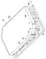
基板42の表面42Bには、抵抗やコンデンサ、半導体チップなどの電子部品56が実装されている。この電子部品56を保護するために、基板42の表面42Bには、箱形状のシールドケース58が取り付けられている。シールドケース58は、金属製のものが用いられており、このシールドケース58を基板42に取り付けることで、基板42上の電子部品56から発生する電磁波はシールドケース58に遮蔽されて、例えば、携帯電話10(図4参照)の通信機能に影響を及ぼさない。
シールドケース58は、平面視にて略長方形で、対向する角部がカットされ短側面58Cが形成された箱形状とされている。この短側面58Cの略中央部から、爪部66が延出されている。爪部66は略矩形状の板状とされ、先端部にR形状が形成されている。
The
一方、基板42の対向する角部近傍には、長円状の孔部62が形成されており、図2に示すように、シールドケース58を基板42上に載置したとき、爪部66が孔部62に挿通されるようになっている。このように、爪部66を孔部62に挿通することで、基板42に対するシールドケース58の位置決めがされる。
On the other hand, an
また、シールドケース58は、天井面58A、側面58B及び短側面58Cを展開した状態で板金から打ち抜く工程と、天井面58Aに対して側面58B、短側面58Cを略直角に折り曲げる工程を経て形成される。このとき、各側面58Bと、側面58Bと短側面58Cの間には隙間が形成される。
Further, the
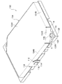
図3は、基板42にシールドケース58を載置したときの、基板42の裏面42Aから見た状態を示す図である。
FIG. 3 is a diagram illustrating a state viewed from the
基板42の裏面42Aの孔部62近傍には、略三角形状のはんだランド68が設けられている。はんだランド68は、基板42に設けられたアース部(図示省略)に接続されている。また、はんだランド68には、基板42の表面42B(実装面)から孔部62に挿通されたシールドケース58の爪部66がはんだ付けによって固定される。これによって、基板42の表面42Bに実装された電子部品56(図1参照)から発生する電磁波は、シールドケース58に伝わってはんだランド68からアース部に吸収される。これにより、電子部品56から発生する電磁波が、携帯電話10(図4参照)の通信機能に影響を及ぼすことを防止できる。
In the vicinity of the
ここで、携帯電話10について簡単に説明する。図4には、本発明の実施形態の基板へのシールドケース取付構造によって基板を用いて形成された撮像モジュール40が搭載された携帯電話10が示されている。
Here, the
図4(A)に示すように、携帯電話10は、液晶画面14とスピーカー15を備えた表示部12と、マイク17を備えた操作部13がヒンジ19で折り畳み自在に連結されている。また、操作部13にはスイッチ16が設けられている。スイッチ16は、各種指示入力を行うためのものである。本実施の形態では、スイッチ16として、撮影ボタン18、電話ボタン20、静止画ボタン22、動画ボタン24、自分撮りボタン26、上下矢印キー28、及びテンキー30が機能する。上下矢印キー28は、液晶画面14または背面液晶画面36(図4(B)参照)に表示された各種メニューから任意のメニュー項目を選択する際にユーザによって操作されるものである。テンキー30は、数字等のデータを入力する際にユーザによって操作されるものである。また、携帯電話10の表示部12の上面には、外部と通信するためのアンテナ32が設けられており、通信部として機能する。
As shown in FIG. 4A, in the
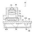
図4(B)に示すように、表示部12には、撮像モジュール40(詳細は後述する)が内臓され、鏡筒48の絞りレンズ50が表示部12の背面に面している。
As shown in FIG. 4B, the
次に、図5に基づいて、撮像モジュール40の構成について説明する。
Next, the configuration of the
撮像モジュール40は、非金属製のセラミックなどで成形された平板状の基板42を備えている。この基板42の一方の面42A(裏面)には、撮像素子としてのCCDイメージセンサーまたはCMOSイメージセンサーなどで構成された撮像用チップ44が配置されている。この撮像用チップ44上には、赤外光(IR)遮光用フィルタ46が配置され、この赤外光遮光用フィルタ46および撮像用チップ44は鏡筒48で覆われている。鏡筒48には、撮像用チップ44上に被写体像を結像する絞りレンズ50と2枚のレンズ52、54が取り付けられている。
The
また、基板42の他方の面42B(表面)には、抵抗やコンデンサ、半導体チップなどの電子部品56が実装されている。この電子部品56を保護するために、基板42の表面42Bには、箱形状のシールドケース58が取り付けられている。
An
次に、本発明の実施形態の作用について説明する。 Next, the operation of the embodiment of the present invention will be described.
図3に示すように、基板42の裏面42A(電子部品56が実装された面と反対側の面)に形成されたはんだランド68に、爪部66をはんだ付けすることで、基板42の表面42Bにシールドケース58を固定するためのスペース、すなわち、はんだランド68を形成するスペースを確保する必要がない。したがって、基板42を小型化することが可能となる。
As shown in FIG. 3, the surface of the
また、基板42の裏面42Aにはんだランド68を形成することで、はんだランド68を十分な大きさにできる。これにより、シールドケース58を基板42に固定させたときの、取り付け強度を高くすることができる。
Moreover, by forming the solder lands 68 on the
さらに、はんだ付け作業で発生するはんだ屑やはんだフラックスは、基板42の裏面42A側に飛散するので、シールドケース58と基板42の隙間から入り込むことがない。
Furthermore, since the solder scraps and solder flux generated in the soldering operation are scattered on the
また、シールドケース58が、板金を折り曲げて作製された、いわゆる、側面58B間及び側面58Bと短側面58Cの間に隙間N(図2参照)がある形状をしている場合でも、はんだ屑やはんだフラックスがシールドケース58内に入り込む恐れがない。したがって、シールドケース58内にはんだ屑やはんだフラックスが入り込むのを阻止するために、シールドケース58をプレス絞り加工で作製する必要がないので、安価にシールドケース58を作成することができ、コストダウンに繋がる。
Even when the
また、基板42に形成された孔部62に、シールドケース58の爪部66を挿通させることで、基板42に対するシールドケース58の位置決めがされる。これにより、シールドケース58の基板42に対する位置決めを行うために、図9に示すような、位置決め用爪114や、この位置決め用爪114を係止させる係止部116を、それぞれシールドケース104や基板102に設ける必要がない。
In addition, the
また、基板42の孔部62に挿通した爪部66にはんだ70を取り付けることで、はんだ70が突起状となって、孔部62から爪部66が外れることを防止する。したがって、シールドケース58が基板42から外れることを防止するための部材等をシールドケース58又は基板42に設ける必要がない。
Further, by attaching the
以上のことから、シールドケース58及び基板42の形状が簡素化されるので、シールドケース58及び基板42の作製コストを抑えることができる。
From the above, since the shapes of the
また、基板42の表面42Bを覆うシールドケース58を、基板42の裏面42Aで基板42に固定させる構成とすることで、シールドケース58に衝撃が加えられても、基板42からシールドケース58が外れにくい構造となる。
In addition, the
ところで、はんだランド68に爪部66をはんだ付けする際に、はんだごて等で爪部66を加熱する必要がある。このとき、図9に示すように、シールドケース104の爪部106を側面104Bに対して略直角に折り曲げて、基板102のIC(電子部品)等が実装された面102Bに設けられたはんだランド108に、この爪部106をはんだ付けする場合、爪部106を加熱しても、その熱はシールドケース104本体から放熱されてしまう。
By the way, when soldering the
そこで、図3に示すように、爪部66を基板42の裏面42A側に突出させ、シールドケース58本体と爪部66の間に基板42を介在させて、はんだランド68に爪部66をはんだ付けする。このとき、爪部66に加えられた熱は、基板42で遮断されてシールドケース58本体へ伝導されにくくなるので、放熱されにくい。したがって、爪部66の加熱性が良くなり、はんだ付けの作業をスムーズに行うことができる。
Therefore, as shown in FIG. 3, the
一方、図9に示す従来のシールドケース104の場合、板金から切り出す工程と、底面104Aに対して側面104Bを略直角に折り曲げる工程と、側面104Bに対して爪部106を折り曲げる工程と、を経て作製される。また、位置決め用爪114と側面104Bの間にはスリット118が形成されている。このスリット118は、板金から切り出す工程で行うことが困難なため、別の工程で形成される。
On the other hand, in the case of the
これに対して、本実施形態のシールドケース58は、板金から切り出す工程と、天井面58Aに対して側面58B、短側面58Cを略直角に曲げる工程のみを経て作製される。したがって、シールドケース58を作製する工程が短いため、作製コストを低く抑えることができる。
On the other hand, the
なお、本実施形態においては、爪部66を基板42の孔部62に挿通させる構成としたが、図6(A)に示すように、基板76の対向する一対の辺に切欠部78を形成し、この切欠部78にシールドケース72に形成された爪部74を固定させ、図6(B)に示すように、基板76の裏面76Aに設けられたはんだランド80に爪部74をはんだ付けしてもよい。また、この場合、切欠部78に固定させた爪部74を基板76側に折り曲げてもよい。これにより、爪部74が切欠部78からはずれにくくなるので、はんだ付け作業が楽になる。
In the present embodiment, the
さらに、本実施形態では、はんだランド68に爪部66をはんだ付けすることで、シールドケース58を基板42に取り付ける構成としたが、図7及び図8に示すように、爪部66に導電性部材で形成されたクリップ84、86を嵌め込み、このクリップ84、86をはんだランド68に接触させる構成としてもよい。このとき、クリップ84、86をはんだ付けする必要がないので、はんだ屑やはんだフラックスの飛散がなく、シールドケース58内にこれらが入り込む恐れがない。また、はんだを用いてシールドケース58を基板42に取り付ける場合と比較して、取り付け作業が単純となる。
Further, in this embodiment, the
40 撮像モジュール
42 基板
62 孔部(挿通部)
66 爪部(突出部)
68 はんだランド(固定部材)
70 はんだ(固定部材)
72 シールドケース
74 爪部(突出部)
76 基板
78 切欠(挿通部)
84 クリップ(固定部材)
86 クリップ(固定部材)
40
66 Claw (protrusion)
68 Solder land (fixing member)
70 Solder (fixing member)
72
76
84 clips (fixing member)
86 Clip (fixing member)
Claims (5)
前記電子部品を覆い、電磁波を遮断するシールドケースと、
前記シールドケースから突出された突出部と、
前記基板に形成され、前記突出部が挿通可能な挿通部と、
前記挿通部に挿通された突出部を前記基板の他方の面で固定する固定部材と、
を有することを特徴とする基板へのシールドケース取付構造。 A board with electronic components mounted on one side;
A shield case that covers the electronic component and blocks electromagnetic waves;
A protruding portion protruding from the shield case;
An insertion part formed on the substrate, through which the protruding part can be inserted, and
A fixing member for fixing the protruding portion inserted through the insertion portion on the other surface of the substrate;
A structure for attaching a shield case to a substrate, comprising:
Priority Applications (6)
| Application Number | Priority Date | Filing Date | Title |
|---|---|---|---|
| JP2005006367A JP2006196664A (en) | 2005-01-13 | 2005-01-13 | Structure for mounting shielding case to substrate and portable phone |
| TW095101140A TW200704359A (en) | 2005-01-13 | 2006-01-12 | Structure and method for attaching shield case to circuit board, electronic component module and portable telephone |
| US11/813,525 US20090016039A1 (en) | 2005-01-13 | 2006-01-13 | Structure And Method For Attaching Shield Case To Circuit Board, Electronic Component Module And Portable Telephone |
| EP06700939A EP1844638A2 (en) | 2005-01-13 | 2006-01-13 | Structure and method for attaching shield case to circuit board, electronic component module and portable telephone |
| PCT/JP2006/300787 WO2006075794A2 (en) | 2005-01-13 | 2006-01-13 | Structure and method for attaching shield case to circuit board, electronic component module and portable telephone |
| CNA2006800023346A CN101103661A (en) | 2005-01-13 | 2006-01-13 | Structure and method for attaching shield case to circuit board, electronic component module and portable telephone |
Applications Claiming Priority (1)
| Application Number | Priority Date | Filing Date | Title |
|---|---|---|---|
| JP2005006367A JP2006196664A (en) | 2005-01-13 | 2005-01-13 | Structure for mounting shielding case to substrate and portable phone |
Publications (1)
| Publication Number | Publication Date |
|---|---|
| JP2006196664A true JP2006196664A (en) | 2006-07-27 |
Family
ID=36678017
Family Applications (1)
| Application Number | Title | Priority Date | Filing Date |
|---|---|---|---|
| JP2005006367A Pending JP2006196664A (en) | 2005-01-13 | 2005-01-13 | Structure for mounting shielding case to substrate and portable phone |
Country Status (6)
| Country | Link |
|---|---|
| US (1) | US20090016039A1 (en) |
| EP (1) | EP1844638A2 (en) |
| JP (1) | JP2006196664A (en) |
| CN (1) | CN101103661A (en) |
| TW (1) | TW200704359A (en) |
| WO (1) | WO2006075794A2 (en) |
Cited By (11)
| Publication number | Priority date | Publication date | Assignee | Title |
|---|---|---|---|---|
| JP2008288523A (en) * | 2007-05-21 | 2008-11-27 | Fujitsu Media Device Kk | Electronic part, and manufacturing method therefor |
| JP2010010524A (en) * | 2008-06-30 | 2010-01-14 | Sharp Corp | Electronic device module |
| JP2010245561A (en) * | 2010-07-13 | 2010-10-28 | Fujitsu Media Device Kk | Method of manufacturing electronic component |
| KR20120023002A (en) | 2009-05-22 | 2012-03-12 | 센주긴조쿠고교 가부시키가이샤 | Solder-coated component, process for producing same, and method for mounting same |
| WO2012176646A1 (en) | 2011-06-23 | 2012-12-27 | Necカシオモバイルコミュニケーションズ株式会社 | Shield frame, sealed frame mounting structure, and electronic portable device |
| JP2013077589A (en) * | 2011-09-29 | 2013-04-25 | Kitagawa Ind Co Ltd | Surface-mounting clip and clipping structure |
| WO2013151152A1 (en) * | 2012-04-06 | 2013-10-10 | Tdk株式会社 | Shield case and electronic apparatus |
| JP2016207961A (en) * | 2015-04-28 | 2016-12-08 | 富士通株式会社 | Printed board and shield plate fixing method |
| CN106358380A (en) * | 2016-08-30 | 2017-01-25 | 浙江中智机器人有限公司 | Automatic shielding cover pressing device for automatic production of circuit board |
| JP2019062083A (en) * | 2017-09-27 | 2019-04-18 | アルプスアルパイン株式会社 | Electronic circuit module |
| JP6525371B1 (en) * | 2018-03-28 | 2019-06-05 | 三菱電機株式会社 | Rotating electrical machine and elevator door apparatus using the same |
Families Citing this family (23)
| Publication number | Priority date | Publication date | Assignee | Title |
|---|---|---|---|---|
| US8359739B2 (en) * | 2007-06-27 | 2013-01-29 | Rf Micro Devices, Inc. | Process for manufacturing a module |
| US8959762B2 (en) | 2005-08-08 | 2015-02-24 | Rf Micro Devices, Inc. | Method of manufacturing an electronic module |
| CN101730459B (en) * | 2008-10-17 | 2013-02-20 | 深圳富泰宏精密工业有限公司 | Shielding case and manufacturing method thereof |
| JP5126244B2 (en) * | 2010-02-12 | 2013-01-23 | 株式会社村田製作所 | Circuit module |
| CN102348345B (en) * | 2010-08-03 | 2016-08-24 | 富泰华工业(深圳)有限公司 | Case of electronic device |
| US9137934B2 (en) | 2010-08-18 | 2015-09-15 | Rf Micro Devices, Inc. | Compartmentalized shielding of selected components |
| US8835226B2 (en) | 2011-02-25 | 2014-09-16 | Rf Micro Devices, Inc. | Connection using conductive vias |
| US9627230B2 (en) | 2011-02-28 | 2017-04-18 | Qorvo Us, Inc. | Methods of forming a microshield on standard QFN package |
| CN103124484B (en) * | 2011-11-21 | 2017-01-25 | 富泰华工业(深圳)有限公司 | Electronic device |
| US8825123B1 (en) | 2012-10-16 | 2014-09-02 | Juan Carlos Gudino | Passthrough case for a smart phone |
| US9462732B2 (en) | 2013-03-13 | 2016-10-04 | Laird Technologies, Inc. | Electromagnetic interference shielding (EMI) apparatus including a frame with drawn latching features |
| US9807890B2 (en) | 2013-05-31 | 2017-10-31 | Qorvo Us, Inc. | Electronic modules having grounded electromagnetic shields |
| US9241097B1 (en) | 2013-09-27 | 2016-01-19 | Amazon Technologies, Inc. | Camera module including image sensor die in molded cavity substrate |
| CN105873423B (en) * | 2016-05-25 | 2019-01-22 | 努比亚技术有限公司 | Shield assembly and its welding procedure |
| US10925160B1 (en) | 2016-06-28 | 2021-02-16 | Amazon Technologies, Inc. | Electronic device with a display assembly and silicon circuit board substrate |
| US10548249B2 (en) * | 2017-09-27 | 2020-01-28 | Intel Corporation | Shielding in electronic assemblies |
| CN107995840A (en) * | 2017-11-16 | 2018-05-04 | 广东欧珀移动通信有限公司 | Shield shell component, terminal device and its assembly method and method for dismounting |
| US11127689B2 (en) | 2018-06-01 | 2021-09-21 | Qorvo Us, Inc. | Segmented shielding using wirebonds |
| US11219144B2 (en) | 2018-06-28 | 2022-01-04 | Qorvo Us, Inc. | Electromagnetic shields for sub-modules |
| US11114363B2 (en) | 2018-12-20 | 2021-09-07 | Qorvo Us, Inc. | Electronic package arrangements and related methods |
| US11515282B2 (en) | 2019-05-21 | 2022-11-29 | Qorvo Us, Inc. | Electromagnetic shields with bonding wires for sub-modules |
| WO2020241474A1 (en) * | 2019-05-31 | 2020-12-03 | 日立オートモティブシステムズ株式会社 | Electronic control device |
| CN115119484A (en) * | 2021-03-18 | 2022-09-27 | 台达电子工业股份有限公司 | Voltage conversion device |
Family Cites Families (18)
| Publication number | Priority date | Publication date | Assignee | Title |
|---|---|---|---|---|
| US4370515A (en) * | 1979-12-26 | 1983-01-25 | Rockwell International Corporation | Electromagnetic interference |
| US4422128A (en) * | 1981-08-06 | 1983-12-20 | General Motors Corporation | Push-on terminal clip and assembly |
| DE8123367U1 (en) * | 1981-08-08 | 1981-12-24 | Standard Elektrik Lorenz Ag, 7000 Stuttgart | Two-part shielding housing for a high-frequency component |
| DE3642151A1 (en) * | 1986-12-10 | 1988-06-23 | Philips Patentverwaltung | Cover (lid) contact-making device on a housing of an RF or IF module |
| US4838475A (en) * | 1987-08-28 | 1989-06-13 | Motorola, Inc. | Method and apparatus for EMI/RFI shielding an infrared energy reflow soldered device |
| US5647748A (en) * | 1995-07-14 | 1997-07-15 | Dell Computer Corporation | Printed circuit board ground clip |
| TW486238U (en) * | 1996-08-18 | 2002-05-01 | Helmut Kahl | Shielding cap |
| US5953217A (en) * | 1997-12-05 | 1999-09-14 | Micron Electronics, Inc. | Contacting element for grounding a printed circuit board to a chassis |
| US6186800B1 (en) * | 1999-01-13 | 2001-02-13 | Micron Electronics, Inc. | Circuit board grounding and support structure |
| US6239359B1 (en) * | 1999-05-11 | 2001-05-29 | Lucent Technologies, Inc. | Circuit board RF shielding |
| JP2001044683A (en) * | 1999-08-02 | 2001-02-16 | Murata Mfg Co Ltd | Shield case and electronic equipment equipped therewith |
| JP2001148594A (en) * | 1999-11-19 | 2001-05-29 | Murata Mfg Co Ltd | Electronic device with shield case |
| JP2003330086A (en) * | 2002-05-09 | 2003-11-19 | Matsushita Electric Ind Co Ltd | Lens switching device and mobile information terminal device |
| US6781851B2 (en) * | 2002-05-30 | 2004-08-24 | Lucent Technologies Inc. | Electromagnetic interference shield |
| DE10231145A1 (en) * | 2002-07-10 | 2004-01-29 | Siemens Ag | Shielding device for electronic assemblies on a printed circuit board |
| US6989994B2 (en) * | 2004-02-26 | 2006-01-24 | Eagle Comtronics, Inc. | Circuit board sub-assemblies, methods for manufacturing same, electronic signal filters including same, and methods, for manufacturing electronic signal filters including same |
| TWM289575U (en) * | 2005-11-04 | 2006-04-11 | Hon Hai Prec Ind Co Ltd | Electromagnetic interference shield device |
| US7351107B1 (en) * | 2007-01-03 | 2008-04-01 | Delphi Technologies, Inc. | One-piece electromagnetic shield having mechanical attachment features |
-
2005
- 2005-01-13 JP JP2005006367A patent/JP2006196664A/en active Pending
-
2006
- 2006-01-12 TW TW095101140A patent/TW200704359A/en unknown
- 2006-01-13 EP EP06700939A patent/EP1844638A2/en not_active Withdrawn
- 2006-01-13 CN CNA2006800023346A patent/CN101103661A/en active Pending
- 2006-01-13 US US11/813,525 patent/US20090016039A1/en not_active Abandoned
- 2006-01-13 WO PCT/JP2006/300787 patent/WO2006075794A2/en active Application Filing
Cited By (15)
| Publication number | Priority date | Publication date | Assignee | Title |
|---|---|---|---|---|
| US8199527B2 (en) | 2007-05-21 | 2012-06-12 | Taiyo Yuden Co., Ltd. | Electronic component and manufacturing method therefor |
| JP2008288523A (en) * | 2007-05-21 | 2008-11-27 | Fujitsu Media Device Kk | Electronic part, and manufacturing method therefor |
| JP2010010524A (en) * | 2008-06-30 | 2010-01-14 | Sharp Corp | Electronic device module |
| KR20160105913A (en) | 2009-05-22 | 2016-09-07 | 센주긴조쿠고교 가부시키가이샤 | Solder-coated component, process for producing same, and method for mounting same |
| KR20120023002A (en) | 2009-05-22 | 2012-03-12 | 센주긴조쿠고교 가부시키가이샤 | Solder-coated component, process for producing same, and method for mounting same |
| JP2010245561A (en) * | 2010-07-13 | 2010-10-28 | Fujitsu Media Device Kk | Method of manufacturing electronic component |
| WO2012176646A1 (en) | 2011-06-23 | 2012-12-27 | Necカシオモバイルコミュニケーションズ株式会社 | Shield frame, sealed frame mounting structure, and electronic portable device |
| JP2013077589A (en) * | 2011-09-29 | 2013-04-25 | Kitagawa Ind Co Ltd | Surface-mounting clip and clipping structure |
| WO2013151152A1 (en) * | 2012-04-06 | 2013-10-10 | Tdk株式会社 | Shield case and electronic apparatus |
| JP2016207961A (en) * | 2015-04-28 | 2016-12-08 | 富士通株式会社 | Printed board and shield plate fixing method |
| CN106358380A (en) * | 2016-08-30 | 2017-01-25 | 浙江中智机器人有限公司 | Automatic shielding cover pressing device for automatic production of circuit board |
| CN106358380B (en) * | 2016-08-30 | 2018-11-02 | 浙江中智机器人有限公司 | It is a kind of for circuit board automated production from dynamic pressure shielding case device |
| JP2019062083A (en) * | 2017-09-27 | 2019-04-18 | アルプスアルパイン株式会社 | Electronic circuit module |
| JP6525371B1 (en) * | 2018-03-28 | 2019-06-05 | 三菱電機株式会社 | Rotating electrical machine and elevator door apparatus using the same |
| WO2019186832A1 (en) * | 2018-03-28 | 2019-10-03 | 三菱電機株式会社 | Dynamo-electric machine, and elevator door device using same |
Also Published As
| Publication number | Publication date |
|---|---|
| US20090016039A1 (en) | 2009-01-15 |
| TW200704359A (en) | 2007-01-16 |
| EP1844638A2 (en) | 2007-10-17 |
| WO2006075794A3 (en) | 2007-02-01 |
| CN101103661A (en) | 2008-01-09 |
| WO2006075794A2 (en) | 2006-07-20 |
Similar Documents
| Publication | Publication Date | Title |
|---|---|---|
| JP2006196664A (en) | Structure for mounting shielding case to substrate and portable phone | |
| JP4762818B2 (en) | Substrate unit manufacturing method, substrate unit, and surface mounting frame unit | |
| US9215360B2 (en) | Camera module having shield can | |
| JP2007274624A (en) | Camera module | |
| KR101128931B1 (en) | Camera module | |
| JP2005094637A (en) | Imaging module, and portable telephone using the same | |
| JP2003283176A (en) | Portable terminal device | |
| JP3782342B2 (en) | Shield case and wireless communication apparatus having the same | |
| CN107613047B (en) | Manufacturing method of electronic assembly, electronic assembly and electronic device | |
| JP2007123214A (en) | Mounting structure of camera module | |
| US20220272868A1 (en) | Electronic device including vapor chamber | |
| KR20090048816A (en) | Structure for assembling shield can camera module | |
| CN107566558B (en) | Method for manufacturing electronic assembly | |
| JP2005159144A (en) | Shielding case | |
| JP2009088754A (en) | High frequency module and communication device using the same | |
| JP4510860B2 (en) | Mobile terminal device | |
| US20050233641A1 (en) | Shield structure of electronic device | |
| JP7450852B2 (en) | photoelectric sensor | |
| JP2012256654A (en) | Circuit board and electronic apparatus | |
| KR101007334B1 (en) | camera module | |
| JP2009071476A (en) | Imaging apparatus and mobile terminal | |
| JP2008288518A (en) | Mounting structure for electronic component module on small-sized electronic equipment | |
| JP2007180857A (en) | Portable electronic equipment | |
| JP2006049710A (en) | Electromagnetic-wave shield frame, and electronic substrate and electronic appliance mounted therewith | |
| JPH1126973A (en) | Electronic apparatus |
Legal Events
| Date | Code | Title | Description |
|---|---|---|---|
| A711 | Notification of change in applicant |
Free format text: JAPANESE INTERMEDIATE CODE: A712 Effective date: 20070221 |