JP2006108398A - Controller and its manufacturing method - Google Patents
Controller and its manufacturing method Download PDFInfo
- Publication number
- JP2006108398A JP2006108398A JP2004293183A JP2004293183A JP2006108398A JP 2006108398 A JP2006108398 A JP 2006108398A JP 2004293183 A JP2004293183 A JP 2004293183A JP 2004293183 A JP2004293183 A JP 2004293183A JP 2006108398 A JP2006108398 A JP 2006108398A
- Authority
- JP
- Japan
- Prior art keywords
- substrate
- metal member
- metal
- electrically connected
- circuit board
- Prior art date
- Legal status (The legal status is an assumption and is not a legal conclusion. Google has not performed a legal analysis and makes no representation as to the accuracy of the status listed.)
- Granted
Links
- 238000004519 manufacturing process Methods 0.000 title claims description 8
- 239000000758 substrate Substances 0.000 claims abstract description 37
- 229910052751 metal Inorganic materials 0.000 claims description 159
- 239000002184 metal Substances 0.000 claims description 159
- 125000006850 spacer group Chemical group 0.000 claims description 23
- 229910000679 solder Inorganic materials 0.000 claims description 15
- 239000000853 adhesive Substances 0.000 claims description 14
- 230000001070 adhesive effect Effects 0.000 claims description 14
- 239000000463 material Substances 0.000 claims description 13
- 239000012778 molding material Substances 0.000 claims description 5
- 229920005989 resin Polymers 0.000 abstract description 43
- 239000011347 resin Substances 0.000 abstract description 43
- 238000007789 sealing Methods 0.000 abstract description 30
- 238000000034 method Methods 0.000 description 14
- XEEYBQQBJWHFJM-UHFFFAOYSA-N Iron Chemical compound [Fe] XEEYBQQBJWHFJM-UHFFFAOYSA-N 0.000 description 10
- 239000000956 alloy Substances 0.000 description 7
- 229910045601 alloy Inorganic materials 0.000 description 6
- 229910052782 aluminium Inorganic materials 0.000 description 6
- XAGFODPZIPBFFR-UHFFFAOYSA-N aluminium Chemical compound [Al] XAGFODPZIPBFFR-UHFFFAOYSA-N 0.000 description 6
- 230000035882 stress Effects 0.000 description 6
- RYGMFSIKBFXOCR-UHFFFAOYSA-N Copper Chemical compound [Cu] RYGMFSIKBFXOCR-UHFFFAOYSA-N 0.000 description 5
- 239000003990 capacitor Substances 0.000 description 5
- 238000004891 communication Methods 0.000 description 5
- 229910052802 copper Inorganic materials 0.000 description 5
- 239000010949 copper Substances 0.000 description 5
- 229910052742 iron Inorganic materials 0.000 description 5
- 238000012546 transfer Methods 0.000 description 5
- 238000010276 construction Methods 0.000 description 4
- 239000003822 epoxy resin Substances 0.000 description 4
- 230000020169 heat generation Effects 0.000 description 4
- 239000007769 metal material Substances 0.000 description 4
- 229920000647 polyepoxide Polymers 0.000 description 4
- 230000017525 heat dissipation Effects 0.000 description 3
- 238000003780 insertion Methods 0.000 description 3
- 230000037431 insertion Effects 0.000 description 3
- JEIPFZHSYJVQDO-UHFFFAOYSA-N iron(III) oxide Inorganic materials O=[Fe]O[Fe]=O JEIPFZHSYJVQDO-UHFFFAOYSA-N 0.000 description 3
- 238000003825 pressing Methods 0.000 description 3
- 238000004078 waterproofing Methods 0.000 description 3
- 230000005540 biological transmission Effects 0.000 description 2
- 239000004020 conductor Substances 0.000 description 2
- 230000000694 effects Effects 0.000 description 2
- 238000010292 electrical insulation Methods 0.000 description 2
- 239000007788 liquid Substances 0.000 description 2
- -1 made of aluminum Chemical compound 0.000 description 2
- 238000005259 measurement Methods 0.000 description 2
- 238000004806 packaging method and process Methods 0.000 description 2
- 230000005855 radiation Effects 0.000 description 2
- 238000005476 soldering Methods 0.000 description 2
- 239000000126 substance Substances 0.000 description 2
- 230000008646 thermal stress Effects 0.000 description 2
- 229920001187 thermosetting polymer Polymers 0.000 description 2
- 238000001721 transfer moulding Methods 0.000 description 2
- 229910000838 Al alloy Inorganic materials 0.000 description 1
- 229910000881 Cu alloy Inorganic materials 0.000 description 1
- 229910000640 Fe alloy Inorganic materials 0.000 description 1
- HBBGRARXTFLTSG-UHFFFAOYSA-N Lithium ion Chemical compound [Li+] HBBGRARXTFLTSG-UHFFFAOYSA-N 0.000 description 1
- 241000221535 Pucciniales Species 0.000 description 1
- 239000000919 ceramic Substances 0.000 description 1
- 239000011248 coating agent Substances 0.000 description 1
- 238000000576 coating method Methods 0.000 description 1
- 239000002826 coolant Substances 0.000 description 1
- 238000001816 cooling Methods 0.000 description 1
- 239000012777 electrically insulating material Substances 0.000 description 1
- 230000005670 electromagnetic radiation Effects 0.000 description 1
- 239000000446 fuel Substances 0.000 description 1
- 229910001416 lithium ion Inorganic materials 0.000 description 1
- 230000007257 malfunction Effects 0.000 description 1
- 238000000465 moulding Methods 0.000 description 1
- 230000002093 peripheral effect Effects 0.000 description 1
- 230000002265 prevention Effects 0.000 description 1
- 230000003449 preventive effect Effects 0.000 description 1
- 239000002994 raw material Substances 0.000 description 1
- 239000004065 semiconductor Substances 0.000 description 1
- 239000000725 suspension Substances 0.000 description 1
- XLYOFNOQVPJJNP-UHFFFAOYSA-N water Substances O XLYOFNOQVPJJNP-UHFFFAOYSA-N 0.000 description 1
Images


Classifications
-
- H—ELECTRICITY
- H05—ELECTRIC TECHNIQUES NOT OTHERWISE PROVIDED FOR
- H05K—PRINTED CIRCUITS; CASINGS OR CONSTRUCTIONAL DETAILS OF ELECTRIC APPARATUS; MANUFACTURE OF ASSEMBLAGES OF ELECTRICAL COMPONENTS
- H05K3/00—Apparatus or processes for manufacturing printed circuits
- H05K3/22—Secondary treatment of printed circuits
- H05K3/28—Applying non-metallic protective coatings
- H05K3/284—Applying non-metallic protective coatings for encapsulating mounted components
-
- H—ELECTRICITY
- H05—ELECTRIC TECHNIQUES NOT OTHERWISE PROVIDED FOR
- H05K—PRINTED CIRCUITS; CASINGS OR CONSTRUCTIONAL DETAILS OF ELECTRIC APPARATUS; MANUFACTURE OF ASSEMBLAGES OF ELECTRICAL COMPONENTS
- H05K5/00—Casings, cabinets or drawers for electric apparatus
- H05K5/0026—Casings, cabinets or drawers for electric apparatus provided with connectors and printed circuit boards [PCB], e.g. automotive electronic control units
- H05K5/0034—Casings, cabinets or drawers for electric apparatus provided with connectors and printed circuit boards [PCB], e.g. automotive electronic control units having an overmolded housing covering the PCB
-
- H—ELECTRICITY
- H05—ELECTRIC TECHNIQUES NOT OTHERWISE PROVIDED FOR
- H05K—PRINTED CIRCUITS; CASINGS OR CONSTRUCTIONAL DETAILS OF ELECTRIC APPARATUS; MANUFACTURE OF ASSEMBLAGES OF ELECTRICAL COMPONENTS
- H05K5/00—Casings, cabinets or drawers for electric apparatus
- H05K5/0026—Casings, cabinets or drawers for electric apparatus provided with connectors and printed circuit boards [PCB], e.g. automotive electronic control units
- H05K5/0082—Casings, cabinets or drawers for electric apparatus provided with connectors and printed circuit boards [PCB], e.g. automotive electronic control units specially adapted for transmission control units, e.g. gearbox controllers
-
- H—ELECTRICITY
- H05—ELECTRIC TECHNIQUES NOT OTHERWISE PROVIDED FOR
- H05K—PRINTED CIRCUITS; CASINGS OR CONSTRUCTIONAL DETAILS OF ELECTRIC APPARATUS; MANUFACTURE OF ASSEMBLAGES OF ELECTRICAL COMPONENTS
- H05K7/00—Constructional details common to different types of electric apparatus
- H05K7/20—Modifications to facilitate cooling, ventilating, or heating
- H05K7/20845—Modifications to facilitate cooling, ventilating, or heating for automotive electronic casings
- H05K7/20854—Heat transfer by conduction from internal heat source to heat radiating structure
-
- B—PERFORMING OPERATIONS; TRANSPORTING
- B29—WORKING OF PLASTICS; WORKING OF SUBSTANCES IN A PLASTIC STATE IN GENERAL
- B29C—SHAPING OR JOINING OF PLASTICS; SHAPING OF MATERIAL IN A PLASTIC STATE, NOT OTHERWISE PROVIDED FOR; AFTER-TREATMENT OF THE SHAPED PRODUCTS, e.g. REPAIRING
- B29C45/00—Injection moulding, i.e. forcing the required volume of moulding material through a nozzle into a closed mould; Apparatus therefor
- B29C45/14—Injection moulding, i.e. forcing the required volume of moulding material through a nozzle into a closed mould; Apparatus therefor incorporating preformed parts or layers, e.g. injection moulding around inserts or for coating articles
- B29C45/14639—Injection moulding, i.e. forcing the required volume of moulding material through a nozzle into a closed mould; Apparatus therefor incorporating preformed parts or layers, e.g. injection moulding around inserts or for coating articles for obtaining an insulating effect, e.g. for electrical components
-
- H—ELECTRICITY
- H05—ELECTRIC TECHNIQUES NOT OTHERWISE PROVIDED FOR
- H05K—PRINTED CIRCUITS; CASINGS OR CONSTRUCTIONAL DETAILS OF ELECTRIC APPARATUS; MANUFACTURE OF ASSEMBLAGES OF ELECTRICAL COMPONENTS
- H05K1/00—Printed circuits
- H05K1/02—Details
- H05K1/0213—Electrical arrangements not otherwise provided for
- H05K1/0215—Grounding of printed circuits by connection to external grounding means
-
- H—ELECTRICITY
- H05—ELECTRIC TECHNIQUES NOT OTHERWISE PROVIDED FOR
- H05K—PRINTED CIRCUITS; CASINGS OR CONSTRUCTIONAL DETAILS OF ELECTRIC APPARATUS; MANUFACTURE OF ASSEMBLAGES OF ELECTRICAL COMPONENTS
- H05K2201/00—Indexing scheme relating to printed circuits covered by H05K1/00
- H05K2201/09—Shape and layout
- H05K2201/09009—Substrate related
- H05K2201/09054—Raised area or protrusion of metal substrate
-
- H—ELECTRICITY
- H05—ELECTRIC TECHNIQUES NOT OTHERWISE PROVIDED FOR
- H05K—PRINTED CIRCUITS; CASINGS OR CONSTRUCTIONAL DETAILS OF ELECTRIC APPARATUS; MANUFACTURE OF ASSEMBLAGES OF ELECTRICAL COMPONENTS
- H05K2201/00—Indexing scheme relating to printed circuits covered by H05K1/00
- H05K2201/10—Details of components or other objects attached to or integrated in a printed circuit board
- H05K2201/10007—Types of components
- H05K2201/10189—Non-printed connector
-
- H—ELECTRICITY
- H05—ELECTRIC TECHNIQUES NOT OTHERWISE PROVIDED FOR
- H05K—PRINTED CIRCUITS; CASINGS OR CONSTRUCTIONAL DETAILS OF ELECTRIC APPARATUS; MANUFACTURE OF ASSEMBLAGES OF ELECTRICAL COMPONENTS
- H05K2201/00—Indexing scheme relating to printed circuits covered by H05K1/00
- H05K2201/20—Details of printed circuits not provided for in H05K2201/01 - H05K2201/10
- H05K2201/2036—Permanent spacer or stand-off in a printed circuit or printed circuit assembly
-
- H—ELECTRICITY
- H05—ELECTRIC TECHNIQUES NOT OTHERWISE PROVIDED FOR
- H05K—PRINTED CIRCUITS; CASINGS OR CONSTRUCTIONAL DETAILS OF ELECTRIC APPARATUS; MANUFACTURE OF ASSEMBLAGES OF ELECTRICAL COMPONENTS
- H05K3/00—Apparatus or processes for manufacturing printed circuits
- H05K3/0058—Laminating printed circuit boards onto other substrates, e.g. metallic substrates
- H05K3/0061—Laminating printed circuit boards onto other substrates, e.g. metallic substrates onto a metallic substrate, e.g. a heat sink
-
- H—ELECTRICITY
- H05—ELECTRIC TECHNIQUES NOT OTHERWISE PROVIDED FOR
- H05K—PRINTED CIRCUITS; CASINGS OR CONSTRUCTIONAL DETAILS OF ELECTRIC APPARATUS; MANUFACTURE OF ASSEMBLAGES OF ELECTRICAL COMPONENTS
- H05K3/00—Apparatus or processes for manufacturing printed circuits
- H05K3/30—Assembling printed circuits with electric components, e.g. with resistor
- H05K3/32—Assembling printed circuits with electric components, e.g. with resistor electrically connecting electric components or wires to printed circuits
- H05K3/321—Assembling printed circuits with electric components, e.g. with resistor electrically connecting electric components or wires to printed circuits by conductive adhesives
-
- H—ELECTRICITY
- H05—ELECTRIC TECHNIQUES NOT OTHERWISE PROVIDED FOR
- H05K—PRINTED CIRCUITS; CASINGS OR CONSTRUCTIONAL DETAILS OF ELECTRIC APPARATUS; MANUFACTURE OF ASSEMBLAGES OF ELECTRICAL COMPONENTS
- H05K3/00—Apparatus or processes for manufacturing printed circuits
- H05K3/30—Assembling printed circuits with electric components, e.g. with resistor
- H05K3/32—Assembling printed circuits with electric components, e.g. with resistor electrically connecting electric components or wires to printed circuits
- H05K3/34—Assembling printed circuits with electric components, e.g. with resistor electrically connecting electric components or wires to printed circuits by soldering
- H05K3/3447—Lead-in-hole components
-
- Y—GENERAL TAGGING OF NEW TECHNOLOGICAL DEVELOPMENTS; GENERAL TAGGING OF CROSS-SECTIONAL TECHNOLOGIES SPANNING OVER SEVERAL SECTIONS OF THE IPC; TECHNICAL SUBJECTS COVERED BY FORMER USPC CROSS-REFERENCE ART COLLECTIONS [XRACs] AND DIGESTS
- Y10—TECHNICAL SUBJECTS COVERED BY FORMER USPC
- Y10T—TECHNICAL SUBJECTS COVERED BY FORMER US CLASSIFICATION
- Y10T29/00—Metal working
- Y10T29/49—Method of mechanical manufacture
- Y10T29/49002—Electrical device making
- Y10T29/49117—Conductor or circuit manufacturing
- Y10T29/49124—On flat or curved insulated base, e.g., printed circuit, etc.
- Y10T29/4913—Assembling to base an electrical component, e.g., capacitor, etc.
- Y10T29/49146—Assembling to base an electrical component, e.g., capacitor, etc. with encapsulating, e.g., potting, etc.
Abstract
Description
本発明は、回路基板上に実装された電子部品を樹脂封止した構成を有する制御装置および製造方法に係り、特に自動車や農耕機や工機や船舶機等に実装される各種コントロールモジュールやセンサモジュールとに用いるに好適な制御装置およびその製造方法に関する。 The present invention relates to a control device and a manufacturing method having a configuration in which an electronic component mounted on a circuit board is sealed with a resin, and in particular, various control modules and sensors mounted on an automobile, an agricultural machine, an industrial machine, a ship machine, and the like. The present invention relates to a control device suitable for use in a module and a manufacturing method thereof.
従来、自動車や農耕機や工機や船舶機等に実装される各種コントロールモジュール(例えば、エンジンコントロールモジュール,モータコントロールモジュール,自動変速機コントロールモジュール等)は、車室内やエンジンルーム内に配置されていた。これらのコントロールモジュールの構造としては、プリント基板上に電子部品を実装し、このプリント基板を金属ベースに固定し、更にカバーを使ったケースで覆う構成のものが一般的である。 Conventionally, various control modules (for example, an engine control module, a motor control module, an automatic transmission control module, etc.) mounted on an automobile, an agricultural machine, an industrial machine, a ship machine, etc. are arranged in a vehicle compartment or an engine room. It was. These control modules generally have a structure in which electronic components are mounted on a printed board, the printed board is fixed to a metal base, and further covered with a case using a cover.
近年、コントロールモジュールをインテークマニホールド等の上に直接取り付ける形式、すなわち、オンエンジン形式のコントロールモジュールが検討されている。プリント基板を用いたコントロールモジュールでは、耐熱性が120℃程度である為、オンエンジン形式には対応出来ない。セラミック基板を用いたコントロールモジュールは耐熱性が高い為、オンエンジン用として用いる事が可能であるが、やや高価である。また、オンエンジン形式のものには、耐熱性だけでなく、車室内やエンジンルーム内のもの以上に、耐振動性や完全気密防水性が求められている。更に、これらの要求は、オンエンジン形式のコントロールモジュールだけでなく、センサモジュール(例えば、圧力センサモジュール,空気流量計モジュール等)にも要求されるものである。 In recent years, a type in which a control module is directly mounted on an intake manifold or the like, that is, an on-engine type control module has been studied. The control module using a printed circuit board cannot handle the on-engine type because the heat resistance is about 120 ° C. A control module using a ceramic substrate has high heat resistance and can be used for on-engine use, but is somewhat expensive. In addition, the on-engine type is required to have not only heat resistance but also vibration resistance and complete hermetic waterproofing than those in the vehicle compartment and engine room. Furthermore, these requirements are required not only for on-engine type control modules but also for sensor modules (for example, pressure sensor modules, air flow meter modules, etc.).
これらの要求を満たす為、プリント基盤を用いて、オンエンジン形式に適用可能なモジュール装置の構成としては、例えば、特許文献1に記載されているように、トランスファモールド実装によって、外部リード端子と基板を一体成形したものが知られている。また、例えば、特許文献2に記載されているように、ペースト状樹脂を加熱硬化する低圧(減圧)成形法により、コネクタと基板を一体成形したものが知られている。また、これらの方法に対して、生産性向上と、小型化と、信頼性の向上を目的とし、熱硬化性樹脂により封止するモジュール装置およびその製造方法が考案されている。
In order to satisfy these requirements, the configuration of a module device that can be applied to an on-engine type using a printed circuit board is, for example, as disclosed in
しかしながら、これらの方法は耐振性や完全気密防水性の為に樹脂封止するというものであって、電子回路の動作信頼性において重要な耐EMC性や電子部品からの発熱した熱を放熱させる方法について考慮されていなかった。また、モジュール製品を自動車や農耕機や工機や船舶機等に取り付ける方法についても十分に考慮されていなかった。 However, these methods are resin-sealing for vibration resistance and complete hermetic waterproofing, and are methods of dissipating heat generated from EMC resistance and electronic components that are important in the operational reliability of electronic circuits. Was not considered. In addition, a method for attaching the module product to an automobile, an agricultural machine, an industrial machine, a ship machine, or the like has not been sufficiently considered.
また、これらの方法で用いる樹脂は、電気的に絶縁物であり、耐EMC性を向上させる為に回路基板に電気的に安定したアースを良好に導く事が出来なかった。更に樹脂は従来のコントロールモジュールでケース材料として一般的に用いられていた鉄やアルミニウムや銅やそれらの合金等の金属材料に比べて、熱伝導率が低く、回路内に高発熱な電子部品を実装出来なかった。更に樹脂は従来のコントロールモジュールでケース材料として一般的に用いられていた鉄やアルミニウムや銅やそれらの合金等の金属材料に比べて外力による強度が低く、耐振動性や耐変形応力に適応する為に取り付け位置や取り付け方法に制限が生じて生産性を悪くしていた。 Further, the resin used in these methods is an electrically insulating material, and it has been impossible to satisfactorily lead an electrically stable ground to the circuit board in order to improve the EMC resistance. In addition, resin is a low heat conductivity compared to metal materials such as iron, aluminum, copper, and their alloys that are generally used as case materials in conventional control modules, and high heat generation electronic components in the circuit. Could not be implemented. In addition, the resin has lower strength due to external force compared to metal materials such as iron, aluminum, copper, and their alloys that are generally used as case materials in conventional control modules, and adapts to vibration resistance and deformation stress. For this reason, the mounting position and the mounting method are limited, which deteriorates productivity.
本発明の目的は、接続用金属端子を有するコネクタと電子回路を樹脂封止したモジュールでありながら、耐EMC性,放熱性,取り付け性を向上させた制御装置を得る事にある。 An object of the present invention is to obtain a control device that has improved resistance to EMC, heat dissipation, and attachment while being a module in which a connector having a metal terminal for connection and an electronic circuit are sealed with a resin.
上記目的は請求項記載の発明により達成される。 The above object can be achieved by the invention described in the claims.
例えば、制御回路を形成する複数の電子部品と、前記制御回路に電気的に接続され、外部にも接続可能なコネクタ端子と、前記コネクタ端子と前記複数の電子部品とが設置された基板と、前記基板と電気的に接続された金属部材と、前記複数の電子部品と前記基板と前記コネクタ端子とをモールドするモールド材とを備えた制御装置。 For example, a plurality of electronic components forming a control circuit, a connector terminal electrically connected to the control circuit and connectable to the outside, a board on which the connector terminal and the plurality of electronic components are installed, A control apparatus comprising: a metal member electrically connected to the substrate; and a molding material that molds the plurality of electronic components, the substrate, and the connector terminal.
かかる構成により、樹脂封止した事による生産性向上と、小型化と、信頼性の向上等の効果を維持しながら、取付にも使用する金属ケースから電気的接点を得る事が出来るので、耐EMC性を向上させる為に必要な電気的に安定したアースを回路基板に良好に導く事が出来る。更に、発熱部品の近くに熱伝導性の高い金属ケースを置く事が出来るので、放熱性を向上させる事が出来る。更に、金属ケースでモジュール装置を取り付けに使用する事から、金属ケースを使った従来のモジュール装置と同様の方法で取り付けが可能となり、この従来のモジュール装置と同等の取り付け性を得る事が出来る。 With this configuration, it is possible to obtain electrical contacts from the metal case that is also used for mounting while maintaining the effects of productivity improvement, miniaturization, and reliability improvement due to resin sealing. It is possible to satisfactorily lead an electrically stable ground necessary for improving the EMC property to the circuit board. Furthermore, since a metal case having high thermal conductivity can be placed near the heat generating component, heat dissipation can be improved. Further, since the module device is used for attachment with the metal case, it can be attached by the same method as the conventional module device using the metal case, and the attachment property equivalent to this conventional module device can be obtained.
樹脂封止したモジュール装置の耐EMC性,放熱性,取り付け性を向上させるという複数の目的を、金属ケースだけを追加する事で生産性や信頼性を損なう事無く同時に実現する事が出来る。 By adding only a metal case, the multiple purposes of improving the EMC resistance, heat dissipation, and mounting of the resin-sealed module device can be realized simultaneously without sacrificing productivity or reliability.
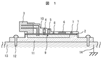
図1は、本発明のモジュール装置の一実施例の形態であって、接続用金属端子を有するコネクタ3と、基板挿入型電子部品4,面実装型大型電子部品5,IC6,高発熱電子部品7,表面搭載チップ型電子部品8,裏面搭載チップ型電子部品9等の電子部品が実装された回路基板2とを有し、前記コネクタ3の基板接続側と前記電子部品とこれらを実装している前記回路基板2とを、同一の樹脂封止部分10によって封止されたモジュール装置1において、金属ケース11を前記モジュール装置1に取り付け、前記金属ケース11と前記回路基板2との電気的導通を得るように形成されている自動車や農耕機や工機や船舶機等に用いられるモジュール装置1の構造断面図である。
FIG. 1 shows an embodiment of a module device according to the present invention. A
このモジュール装置1は、ネジ12等の固定部品によってエンジンや車両ボディ等の金属取り付け面13に固定される。前記エンジンや車両ボディ等の金属取り付け面13は通常各種電子機器の基準アース14として用いられる。
The
通常のモジュール装置1が動作する事により、それ自身から電磁気的放射ノイズを放射し、これによりラジオやテレビ等のような電磁波を受信する装置だけでなく、各種電子装置の動作を妨げるので、前記放射ノイズを他の機器に対し影響が無いレベルまで低減する事が要求される。更に通常のモジュール装置は、無線通信機や携帯電話等のように電磁波を放射する目的の装置から放射された強い電磁波を受けても誤動作しない事が要求される。これらEMC特性を向上する為に、回路基板2上でもコンデンサやインダクタンス等を使用したり、回路パターンを最適化する等して対応しているが、こういった工夫をより有効なものにする為に、本モジュール装置1やその他の装置の動作に影響されない安定した基準アース14を回路基板2内に引き込む事が有効である。
Since the
この目的の為に、前記回路基板2と前記金属ケース11との電気的接点は、インダクタンスやインピーダンスを最小にして接続するのが理論的に最も有効であり、基板全面で接触するのが良い。しかし、回路基板2の面積の制限から現実的には、回路基板2の外周全体での接触や、コネクタ3を挟んで基板両サイドでの接触、コネクタ3との対向側での接触、コネクタ3側での接触、回路基板2に4ヶ所存在する角部分の全て或いはその一部での接触、回路基板2の周囲で無く内側での接触、或いはこれらを組み合わせた接触面での接触でも十分有効であり、この事は従来の樹脂モールドされないモジュール装置と同様である。
For this purpose, it is theoretically most effective to connect the electrical contacts between the
このようにして前記金属ケース11を使用する事で、前記金属ケース11と、前記回路基板2上に実装されているマイクロコンピュータや電源ICやIPD等のIC6や、パワートランジスタやパワーFETやパワーダイオード等の高発熱電子部品7や、場合によっては電解コンデンサやインダクタンス等の基板挿入型電子部品4や、電解コンデンサやインダクタンス等の面実装型大型電子部品5や、チップ抵抗やチップコンデンサ等の表面搭載チップ型電子部品8や、チップ抵抗やチップコンデンサ等の裏面搭載チップ型電子部品9といった発熱する電子部品との熱伝達距離が短くなり、熱伝達面積も広げる事が出来るようになるので、前記電子部品の動作によって発生する熱を、熱伝導率の良い鉄やアルミニウムや銅やそれらの合金等の金属材料で出来た前記金属ケース11を通して、効率良く外部に放出させる事が可能になる。
By using the
更には、前記金属ケース11を意図的に前記発熱する電子部品に接触或いは、電気的にこの電子部品と金属ケース11間の絶縁が必要な場合は、その間に絶縁シートや絶縁接着剤を挟み込んだり樹脂封止部分10の封止時にこの樹脂を流し込む事で、電気的絶縁を維持出来る最小距離まで金属ケース11と発熱する電子部品を近づけて、熱伝達特性を向上させる事も可能である。また、前記金属ケース11を放熱フィン状の構造として空気等の気体状媒体との接触面積を広げたり、金属ケース11内に水等の液状の冷却媒体を流通させる事が出来る通路を設ける事で、冷却特性を向上させる事が可能になる。
Further, when the
前記回路基板2の主材料と前記樹脂封止部分10の熱膨張率の違いによる熱応力によるモジュール装置1の破損を防ぐ為に、前記樹脂封止部分10に用いられる樹脂の熱膨張係数は前記回路基板2の主材料と可能な限り近いものを使用するのが望ましい。前記回路基板2にエポキシ樹脂を主材料としたプリント基板を使用した時には、前記樹脂封止部分
10の熱膨張係数は、熱硬化性樹脂の内、半導体封止に用いられるトランスファーモールド用エポキシ樹脂の8〜18×10-6/Kの間となる。また、前記金属ケース11は、熱膨張率だけであれば、銅又は銅を主原料とした銅合金材料が前記プリント基板や前記トランスファーモールド用エポキシ樹脂に近く、16〜20×10-6/K程度であり望ましいが、錆び易い欠点があるので、モジュール装置1の搭載条件を加味して防錆コーティングする等して用いるのが望ましい。また従来の樹脂モールドされないモジュール装置と同様に防錆やコストの観点からアルミニウムやアルミニウムを主原料とした合金や鉄や鉄を主原料とした合金や防錆コーティングされた前記鉄合金を用いる事も可能である。前記トランスファーモールド用エポキシ樹脂で封止したモジュールでは、特に熱膨張率が21〜
25×10-6/Kである前記アルミニウムを主原料とした合金が望ましい。この時に前記樹脂封止部分10の樹脂封止時の流れ性が良く、使用する前記アルミニウム合金との熱膨張率の差が小さく、前記回路基板2や接続用金属端子を有するコネクタ3のハウジング材料や、各種電子部品との接着力が良い樹脂材料を選択するのが望ましい。
In order to prevent damage to the
An alloy having 25 × 10 −6 / K as the main raw material for aluminum is desirable. At this time, the
以上のような金属材料で出来た前記金属ケース11は、従来の樹脂モールドされないモジュール装置と同じ方法によって、エンジンや車両ボディ等の金属取り付け面13に固定する事が出来る。その方法は、例えば図1記載のように金属ケース11を直接エンジンや車両ボディ等の金属取り付け面13に接触させて、モジュール装置固定用ネジ12によって固定する事が出来る。または、耐振動性向上や取付応力低減の目的で、前記金属ケース11と前記エンジンや車両ボディ等の金属取り付け面13との間に、金属ブラケットを配置して、ネジ等によって固定する事も出来る。
The
前記金属ケース11は、図1のようにモジュール装置1の下部全面だけに配置する事も出来るが、耐電波性や耐衝撃性向上等の目的で、モジュール装置1全体を覆うようにより広い面積に配置する事も出来、或いは前記樹脂封止部分10でモジュール装置1が保護されているので、実使用状態における前記樹脂封止部分10の耐振動性等に対する強度を考慮する事で、前記金属ケース11と前記樹脂封止部分10の接続力向上の目的で、前記金属ケース11に開口部を設けて前記樹脂封止部分10を入れ込む構造としてより狭い面積に配置したり、前記金属ケース11のコスト低減の目的で、単純に前記金属ケース11に開口部を広げたりサイズを縮小してより狭い面積に配置する事も出来る。また、金属ケース11は、コネクタ3の配置部に対して下部だけで無く、上部に配置したり、コネクタ3の対向側やコネクタ3の周囲等に配置する事も可能である。
Although the
更に、以上の構造を有しているモジュール装置1において、気圧や空気流量や温度等を測定するセンサの測定部分のみを外部に出して樹脂封止する事で、前記気圧や空気流量や温度等のセンサ機能を得る事も出来る。特に気圧センサとしての目的ではコネクタ3に通気口を設けてモジュール装置1の内部に測定する気体を導く事で気圧センサ機能を得る事が出来る。
Further, in the
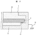
図2は、本発明のモジュール装置の一実施例の形態であって、実施例1の構造において、金属ケース11の周囲形状を「コ」の字型とし、その間に前記金属ケース11と接触させた回路基板2を挿入して、樹脂封止部分10を高温で樹脂封止して通常使用温度まで冷却する事によって、前記金属ケース11の熱膨張率が前記樹脂封止部分10のそれよりも大きい為に、前記金属ケース11から前記金属ケース11と前記回路基板2の間を押え付ける熱応力が発生し、特別な部品を使用する事なく、基準アース14に接続している前記金属ケース11と前記回路基板2との電気的導通を実施例1の形態よりも効果的に得る為の手段を有した自動車や農耕機や工機や船舶機等に用いられるモジュール装置1の構造断面図である。
FIG. 2 shows an embodiment of the module device according to the present invention. In the structure of the first embodiment, the shape of the
実施例1記載の前記樹脂封止部分10と前記金属ケース11との合わせの場合、前記樹脂封止部分10に対して前記金属ケース11の熱膨張率が高くなるので、前記図2のような構成で前記金属ケース11と前記回路基板2との十分な電気的導通を得る事が可能である。
In the case of combining the resin-encapsulated
もし、前記樹脂封止部分10の熱膨張率が前記のそれよりも高い又は、前記金属ケース11の熱膨張率が前記のそれよりも低い等して、前記樹脂封止部分10に対して前記金属ケース11の熱膨張率が低くなったとしても、図2とは逆に前記回路基板2と接触した前記金属ケース11の周囲に前記樹脂封止部分10を囲い込むように樹脂封止する事で、今度は前記樹脂封止部分10から前記金属ケース11と前記回路基板2の間を押え付ける応力が発生し、同様に特別な部品を使用する事なく、実施例1の形態よりも効果的に基準アース14に接続している前記金属ケース11と前記回路基板2との電気的導通を得る事が可能である。
If the thermal expansion coefficient of the
更に、前記金属ケース11と前記回路基板2との電気的導通を良好なものとする為に、前記回路基板2に、図2のように電導性物質であるはんだや電導性接着剤等15を塗布した後に、前記樹脂封止を行う事も可能である。
Further, in order to improve the electrical continuity between the
前記金属ケース11は、実施例1と同様な搭載位置を選択する事が出来るが、構造上前記モジュール装置1の外周に前記金属ケース11がある必要がある。この時、前記金属ケース11と前記回路基板2との電気的導通を得る場所もモジュール装置1の外周となるが、実施例1記載の方法と同様に、その導通部分はモジュール装置1の製品条件によって選択する事が出来る。
Although the mounting position of the
また、前記電気的導通を得る為に塗布される前記はんだや電導性接着剤等15の塗布形状は、電気的導通を得る為には、広い面積で導通して、インピーダンスやインダクタンスを低く押さえるのが望ましいが、塗布時に液体である前記はんだや電導性接着剤等15の高さ精度は面積が広いと制御し難くなる。この為、複数の塗布部分を設け、それぞれの塗布部分は高さ制御が出来る限度程度の広さに押さえて塗布するのが望ましい。 Moreover, in order to obtain electrical continuity, the application shape of the solder, conductive adhesive 15 or the like applied to obtain the electrical continuity can be conducted over a wide area to keep impedance and inductance low. However, it is difficult to control the height accuracy of the solder or conductive adhesive 15 that is liquid at the time of application if the area is large. For this reason, it is desirable to provide a plurality of application portions, and to apply each of the application portions while suppressing the height to the extent that the height can be controlled.
図3は、本発明のモジュール装置の一実施例の形態であって、実施例1の構造において、金属ケース11と回路基板2の接触を、従来の樹脂モールドされないモジュール装置と同様に金属ケース固定用ネジ16によって、前記金属ケース11と前記回路基板2の間を押え付ける応力が発生し、基準アース14に接続している前記金属ケース11と前記回路基板2との電気的導通を実施例1の形態よりも効果的に得る為の手段を有した自動車や農耕機や工機や船舶機等に用いられるモジュール装置1の構造断面図である。
FIG. 3 shows an embodiment of the module device according to the present invention. In the structure of the first embodiment, the
前記金属ケース11は、実施例1と同様な搭載位置を選択する事が出来るが、前記金属ケース固定用ネジ16を前記回路基板2を通す為に、前記ネジ16の本数が多いと、前記回路基板2上に実装される電子部品の搭載面積が限られてしまう。この為、前記ネジ16の本数は、前記回路基板2の回路構成から前記金属ケース11と前記回路基板2との電気的導通を効果的に得る事が出来、前記回路基板2に実装された各種発熱部品からの放熱の為に、前記金属ケース11と前記回路基板2との距離を最小に保つ事が出来、前記金属ケース11と前記回路基板2との保持力を十分得る事が出来る搭載位置である条件の中で最小の1〜6本程度の本数である事が望ましい。
The mounting position of the
更に、実施例2と同様に、前記金属ケース11と前記回路基板2との電気的導通を良好なものとする為に、前記回路基板2に、図2のように電導性物質であるはんだや電導性接着剤等15を塗布した後に、前記金属ケース固定用ネジ16で前記金属ケース11と前記回路基板2を固定して、前記樹脂封止を行う事も可能である。
Furthermore, in order to improve the electrical continuity between the
図4は、本発明のモジュール装置の一実施例の形態であって、実施例1の構造において、金属ケース11と回路基板2との電気的導通を得る為の手段として、前記回路基板2に金属バネ17を取り付けた後、前記回路基板2と前記バネ17とを一体樹脂封止し、この時前記バネ17の開放端を前記封止に使用した樹脂の外部に出し、この前記バネ17の開放端を金属ケース11と接触させる事で、基準アース14に接続している前記金属ケース11と前記回路基板2との電気的導通を実施例1の形態よりも効果的に得る為の手段を有した自動車や農耕機や工機や船舶機等に用いられるモジュール装置1の構造断面図である。
FIG. 4 shows an embodiment of the module device according to the present invention. In the structure of the first embodiment, the
更に、前記バネ17の開放端と前記金属ケース11との接触安定性を向上させる為に、樹脂封止されたモジュール装置1を前記金属ケース11と保持用カバー18で挟み込み、挟み込み応力をネジ16によって前記金属ケース11と前記保持用カバー18間に発生させる方法が有効である。
Further, in order to improve the contact stability between the open end of the
前記金属バネ17は、前記樹脂封止部分10で樹脂封止する際に、前記回路基板2に押え付けておく事で、固定する事も出来るが、前記回路基板2に実装される各種電子部品と同様に、前記回路基板2にはんだや電導性接着剤等で固定してから樹脂封止する事も出来る。この時、前記バネ17の形状やそのパッケージ方法を自動実装機に対応する事で、容易に前記回路基板2に実装する事が出来る。更に、樹脂封止する時に前記金属バネ17を樹脂封止用型に押え付けておく事で、前記金属バネ17の伸びを要求された寸法内に収める事が出来る。
The
また、前記金属バネ17は、その電気的接触を確実にする為、前記金属ケース11と前記保持用カバー18で挟み込まれた部分内の挟み込み力が強い個所に配置するのが望ましいが、前記金属ケース11と前記保持用カバー18の配置によっては、前記保持用カバー18が無く前記金属ケース11のみの部分であっても、十分な挟み込み力を発生出来るので、そのような場所にも前記金属バネ17を配置する事が可能である。
The
本実施例においては、実施例1,2記載の方法のように、前記金属ケース11を前記樹脂封止部分10で一体樹脂封止する必要が無いので、前記樹脂封止部分10の熱膨張率等の特性を前記金属ケース11に合わせる必要が無く、耐熱サイクル性に強いモジュール装置1を提供する事が可能である。
In the present embodiment, unlike the methods described in the first and second embodiments, it is not necessary to integrally seal the
前記金属ケース11は、実施例1と同様な搭載位置を選択する事が出来るが、前記保持用カバー18は前記モジュール装置1の周辺部にある事が望ましい。また、耐電波性や耐衝撃性向上や防水性向上等の目的で、前記保持用カバー18は前記モジュール装置1の周辺部だけでなく、前記金属ケース11の対面側全体に渡って配置する事も出来、前記実施例1記載の金属ケース11の配置と同様に特定の部分に限定して配置する事も出来る。
Although the mounting position of the
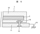
図5は、本発明のモジュール装置の一実施例の形態であって、実施例1の構造において、金属ケース11と回路基板2との電気的導通を得る為の手段として、前記回路基板2に金属スペーサ19を取り付けた後、前記回路基板2と前記金属スペーサ19とを一体樹脂封止し、この時前記金属スペーサ19の開放端を前記封止に使用した樹脂の外部に出し、この前記金属スペーサ19の開放端を金属ケース11と接触させる事で、基準アース14に接続している前記金属ケース11と前記回路基板2との電気的導通を実施例1の形態よりも効果的に得る為の手段を有した自動車や農耕機や工機や船舶機等に用いられるモジュール装置1の構造断面図である。
FIG. 5 shows an embodiment of the module device according to the present invention. In the structure of the first embodiment, the
更に、前記金属スペーサ19の開放端と前記金属ケース11との接触安定性を向上させる為に、前記金属ケース11と前記金属スペーサ19の間を金属ケース固定用ネジ16によって固定する事が可能であり、前記金属スペーサ19の中間部の周囲に円盤状の突起を設ける事で、樹脂封止部分10との接着力や勘合力を高め、小型の前記金属スペーサ19でも十分な強度を持たせる事が可能である。
Further, in order to improve the contact stability between the open end of the
前記金属スペーサ19は、前記樹脂封止部分10で樹脂封止する際に、前記回路基板2に押え付けておく事で、固定する事も出来るが、前記回路基板2に実装される各種電子部品と同様に、前記回路基板2にはんだや電導性接着剤等で固定してから樹脂封止する事も出来る。この時、前記金属スペーサ19の形状やそのパッケージ方法を自動実装機に対応する事で、容易に前記回路基板2に実装する事が出来る。はんだ付け時には、取り付け状態での前記金属スペーサ19の高さ精度を管理する為に、はんだペースト等によってはんだ量をコントロール出来るようにしてはんだ付けする事が望ましい。
The
本実施例においては、実施例4と同様に、前記金属ケース11を前記樹脂封止部分10で一体樹脂封止する必要が無いので、前記樹脂封止部分10の熱膨張率等の特性を前記金属ケース11に合わせる必要が無く、耐熱サイクル性に強いモジュール装置1を提供する事が可能である。
In the present embodiment, similarly to the fourth embodiment, since it is not necessary to integrally seal the
前記金属スペーサ19は、前記金属ケース11を実施例1と同様な搭載位置を選択した上で、前記金属ケース11と前記回路基板2によって挟まれた任意の部分の内、前記金属ケース11と前記回路基板2との間の寸法が、前記金属ケース固定用ネジ16の取り付けによって前記金属スペーサ19や前記ネジ16に過大な応力がかからない程度に管理されている部分に配置可能である。
The
図6は、本発明のモジュール装置の一実施例の形態であって、実施例1の構造において、金属ケース11と回路基板2との電気的導通を得る為の手段として、前記金属ケース
11とネジ貫通用穴を開けた前記回路基板2とを接触するように配置した接触面と垂直方向に向かって、貫通穴が開くように樹脂封止部分10で前記金属ケース11と一体樹脂封止した後、前記金属ケース11と反対方向からネジ16を前記貫通穴を通して、前記金属ケース11と固定する事で、前記金属ケース11と前記回路基板2との電気的導通を得る事が出来、基準アース14に接続している前記金属ケース11と前記回路基板2との電気的導通を実施例1の形態よりも効果的に得る為の手段を有した自動車や農耕機や工機や船舶機等に用いられるモジュール装置1の構造断面図である。
FIG. 6 shows an embodiment of the module device according to the present invention. In the structure of the first embodiment, as a means for obtaining electrical continuity between the
更に、前記ネジ16と前記樹脂封止部分10の間に面積の広いモジュール保持用ワッシャ20を挟み込む事で、前記樹脂封止部分10に過大な応力を与えずに、前記金属ケース11と前記回路基板2との電気的導通を得る為の挟み込み力を発生させる事が出来、前記回路基板2と前記金属ケース11間の電気的導通を向上させる為に、前記回路基板2に塗布されたはんだ又は電導性接着剤15を介する事が有効である。
Further, by inserting a
特に本実施例においては、前記金属ケース11の前記ネジ16用穴を貫通穴とし、前記金属ケース11とエンジンや車両ボディ等の金属取り付け面13の間に、実施例1記載のようにブラケットを配置する事で、前記ネジ16によって、前記回路基板2には直接応力を与える事なく、前記ブラケットと前記モジュール装置1を固定すると同時に、前記回路基板2と前記金属ケース11間の締め付け力を発生させて電気的導通を得る事が出来る。また、同様の構造でブラケットを介さずに前記エンジンや車両ボディ等の金属取り付け面13に直接固定する事も出来る。
In particular, in this embodiment, the hole for the
この時、前記回路基板2を貫通する形状で前記ネジ16が取り付けられる為、前記回路基板2の面積が増大するが、前記モジュール装置1の大きさや実施例1の図1に記載されている金属ケース11のエンジンや車両ボディ等の金属取り付け面13との省略可能になった固定用面積によっては、前記モジュール装置1を小型化する事も出来る。
At this time, since the
本発明によるモジュール装置によれば、従来からある各種コントロールモジュール(例えば、エンジンコントロールモジュール,モータコントロールモジュール,自動変速機コントロールモジュール等)やセンサモジュール(例えば、圧力センサモジュール,空気流量計モジュール等)の生産性向上と、小型化と、信頼性の向上等の効果を容易に得る事が出来、更には今後発展すると考えられているアクティブセーフティ機能を提供する各種コントロールモジュール(ブレーキコントロールモジュール,サスペンションコントロールモジュール,ステアリングコントロールモジュール,エアバッグコントロールモジュール,シートベルトコントロールモジュール,車間距離計測モジュール等)や、ITS等の機能を得る為に車両外部と電波により情報交換する各種電子モジュール(携帯電話通信モジュール,ETC通信モジュール,GPS通信モジュール,VICS通信モジュール等)や、耐薬品性が高い為に、化学変化を利用した機器の各種コントロールモジュール(燃料電池コントロールモジュール,リチウムイオン電池充放電コントロールモジュール等)をコスト低減しながら搭載自由度を拡大する事が出来る。 According to the module device of the present invention, various conventional control modules (for example, an engine control module, a motor control module, an automatic transmission control module, etc.) and sensor modules (for example, a pressure sensor module, an air flow meter module, etc.) Various control modules (brake control module, suspension control module) that can easily obtain the effects of productivity improvement, downsizing, improved reliability, etc., and also provide active safety functions that are expected to develop in the future , Steering control module, airbag control module, seat belt control module, inter-vehicle distance measurement module, etc.) Various electronic modules (cell phone communication modules, ETC communication modules, GPS communication modules, VICS communication modules, etc.) that exchange information, and various control modules (fuel cell control) that use chemical changes due to high chemical resistance Module, lithium-ion battery charge / discharge control module, etc.) can be installed at a lower cost.
1…樹脂封止したモジュール装置、2…回路基板、3…接続用金属端子を有するコネクタ、4…基板挿入型電子部品、5…面実装型大型電子部品、6…IC、7…高発熱電子部品、8…表面搭載チップ型電子部品、9…裏面搭載チップ型電子部品、10…樹脂封止部分、11…金属ケース、12…モジュール装置固定用ネジ、13…エンジンや車両ボディ等の金属取り付け面、14…基準アース。
DESCRIPTION OF
Claims (19)
前記制御回路に電気的に接続され、外部にも接続可能なコネクタ端子と、
前記コネクタ端子と前記複数の電子部品とが設置された基板と、
前記基板と電気的に接続された金属部材と、
前記複数の電子部品と前記基板と前記コネクタ端子とをモールドするモールド材とを備えた制御装置。 A plurality of electronic components forming a control circuit;
A connector terminal electrically connected to the control circuit and connectable to the outside;
A board on which the connector terminals and the plurality of electronic components are installed;
A metal member electrically connected to the substrate;
A control apparatus comprising: a molding material that molds the plurality of electronic components, the substrate, and the connector terminal.
前記基板に溶接され、前記複数の電子部品と前記基板と前記コネクタ端子と共にモールドされた半田を備え、
前記半田を介して、前記基板と前記金属部材とが電気的に接続されたことを特徴とする制御装置。 In claim 1,
Solder welded to the substrate, molded with the plurality of electronic components, the substrate and the connector terminal,
A control device, wherein the substrate and the metal member are electrically connected via the solder.
前記基板に固定され、前記複数の電子部品と前記基板と前記コネクタ端子と共にモールドされた金属スペーサを備え、
前記金属スペーサを介して、前記基板と前記金属部材とが電気的に接続されたことを特徴とする制御装置。 In claim 1,
A metal spacer fixed to the substrate and molded with the plurality of electronic components, the substrate and the connector terminal,
The control apparatus, wherein the substrate and the metal member are electrically connected via the metal spacer.
前記金属スペーサには凸部または凹部が設けられたことを特徴とする制御装置。 In claim 3,
The metal spacer is provided with a convex portion or a concave portion.
前記金属スペーサと前記金属部材とがネジにより固定され、
前記ネジを介して、前記基板と前記金属部材とが電気的に接続されたことを特徴とする制御装置。 In claim 3,
The metal spacer and the metal member are fixed by screws,
The control device, wherein the substrate and the metal member are electrically connected via the screw.
前記基板の一部が前記モールド材の外へ露出し、
前記露出した基板と前記金属部材とを接着する導電性接着剤を備え、
前記導電性接着剤を介して、前記基板と前記金属部材とが電気的に接続されたことを特徴とする制御装置。 In claim 1,
A portion of the substrate is exposed outside the mold material;
A conductive adhesive for bonding the exposed substrate and the metal member;
The control apparatus, wherein the substrate and the metal member are electrically connected via the conductive adhesive.
前記制御回路に電気的に接続され、外部にも接続可能なコネクタ端子と、
前記コネクタ端子と前記複数の電子部品とが設置された基板と、
前記基板と電気的に接続され、前記モールド材の一部の領域を挟むように構成された金属部材と、
前記複数の電子部品と前記基板と前記コネクタ端子とをモールドするモールド材とを備えた制御装置。 A plurality of electronic components forming a control circuit;
A connector terminal electrically connected to the control circuit and connectable to the outside;
A board on which the connector terminals and the plurality of electronic components are installed;
A metal member electrically connected to the substrate and configured to sandwich a part of the mold material; and
A control apparatus comprising: a molding material that molds the plurality of electronic components, the substrate, and the connector terminal.
前記金属部材は少なくとも2ヶ所以上で前記基板と電気的に接続されたことを特徴とする制御装置。 In claim 7,
The control apparatus characterized in that the metal member is electrically connected to the substrate at at least two places.
前記領域で、前記基板と前記金属部材とが電気的に接続されたことを特徴とする制御装置。 In claim 8,
The control device, wherein the substrate and the metal member are electrically connected in the region.
前記モールド材の熱膨張係数が、前記金属部材の熱膨張係数よりも小さな場合は、金属をモールド材が挟み込むようにしたことを特徴とする制御装置。 In claim 8,
The control apparatus according to claim 1, wherein when the thermal expansion coefficient of the mold material is smaller than the thermal expansion coefficient of the metal member, the metal is sandwiched between the mold materials.
前記基板に溶接され、前記複数の電子部品と前記基板と前記コネクタ端子と共にモールドされた半田を備え、
前記半田を介して、前記基板と前記金属部材とが電気的に接続されたことを特徴とする制御装置。 In claim 7,
Solder welded to the substrate, molded with the plurality of electronic components, the substrate and the connector terminal,
A control device, wherein the substrate and the metal member are electrically connected via the solder.
前記基板に固定され、前記複数の電子部品と前記基板と前記コネクタ端子と共にモールドされた金属スペーサを備え、
前記金属スペーサを介して、前記基板と前記金属部材とが電気的に接続されたことを特徴とする制御装置。 In claim 7,
A metal spacer fixed to the substrate and molded with the plurality of electronic components, the substrate and the connector terminal,
The control apparatus, wherein the substrate and the metal member are electrically connected via the metal spacer.
前記金属スペーサには凸部または凹部が設けられたことを特徴とする制御装置。 In claim 12,
The metal spacer is provided with a convex portion or a concave portion.
前記金属スペーサと前記金属部材とがネジにより固定され、
前記ネジを介して、前記基板と前記金属部材とが電気的に接続されたことを特徴とする制御装置。 In claim 12,
The metal spacer and the metal member are fixed by screws,
The control device, wherein the substrate and the metal member are electrically connected via the screw.
前記露出した基板と前記金属部材とを接着する導電性接着剤を備え、
前記導電性接着剤を介して、前記基板と前記金属部材とが電気的に接続されたことを特徴とする制御装置。 In claim 7,
A conductive adhesive for bonding the exposed substrate and the metal member;
The control apparatus, wherein the substrate and the metal member are electrically connected via the conductive adhesive.
モールド材によって、前記複数の電子部品と前記基板と前記コネクタ端子とをモールドし、
前記制御回路と金属部材とを電気的に接続した制御装置の製造方法。 A control circuit is formed by connecting a plurality of electronic components and connector terminals connectable to the outside to a board on which wiring is formed,
The molding material molds the plurality of electronic components, the substrate, and the connector terminal,
A control device manufacturing method in which the control circuit and a metal member are electrically connected.
前記制御回路と金属部材とを電気的に接続した後に、
前記モールド材の少なくとも一部を挟む様に、部品を前記金属部材に固定したことを特徴とする制御装置の製造方法。 In claim 16,
After electrically connecting the control circuit and the metal member,
A method of manufacturing a control device, wherein a component is fixed to the metal member so as to sandwich at least a part of the mold material.
半田,スペーサまたはバネを、前記モールド材によって、前記複数の電子部品と前記基板と前記コネクタ端子と同時にモールドし、
前記半田,スペーサまたはバネを介して前記制御回路と金属部材とを電気的に接続したことを特徴とする制御装置の製造方法。 In claim 16,
Solder, spacer or spring is molded by the molding material simultaneously with the plurality of electronic components, the substrate and the connector terminal,
A control device manufacturing method, wherein the control circuit and a metal member are electrically connected via the solder, a spacer, or a spring.
前記制御回路と金属部材とを2ヶ所以上で電気的に接続した制御装置の製造方法。 In claim 16,
A control device manufacturing method in which the control circuit and the metal member are electrically connected at two or more locations.
Priority Applications (5)
| Application Number | Priority Date | Filing Date | Title |
|---|---|---|---|
| JP2004293183A JP4585828B2 (en) | 2004-10-06 | 2004-10-06 | Control device and manufacturing method thereof |
| US11/243,319 US7359212B2 (en) | 2004-10-06 | 2005-10-05 | Control device and method of manufacturing thereof |
| DE602005019961T DE602005019961D1 (en) | 2004-10-06 | 2005-10-06 | Control device and method for its manufacture |
| EP05021840A EP1646271B1 (en) | 2004-10-06 | 2005-10-06 | Control device and method of manufacturing thereof |
| US12/039,472 US7924572B2 (en) | 2004-10-06 | 2008-02-28 | Control device and method of manufacturing thereof |
Applications Claiming Priority (1)
| Application Number | Priority Date | Filing Date | Title |
|---|---|---|---|
| JP2004293183A JP4585828B2 (en) | 2004-10-06 | 2004-10-06 | Control device and manufacturing method thereof |
Publications (2)
| Publication Number | Publication Date |
|---|---|
| JP2006108398A true JP2006108398A (en) | 2006-04-20 |
| JP4585828B2 JP4585828B2 (en) | 2010-11-24 |
Family
ID=35686509
Family Applications (1)
| Application Number | Title | Priority Date | Filing Date |
|---|---|---|---|
| JP2004293183A Active JP4585828B2 (en) | 2004-10-06 | 2004-10-06 | Control device and manufacturing method thereof |
Country Status (4)
| Country | Link |
|---|---|
| US (2) | US7359212B2 (en) |
| EP (1) | EP1646271B1 (en) |
| JP (1) | JP4585828B2 (en) |
| DE (1) | DE602005019961D1 (en) |
Cited By (11)
| Publication number | Priority date | Publication date | Assignee | Title |
|---|---|---|---|---|
| WO2009001752A1 (en) * | 2007-06-26 | 2008-12-31 | Yanmar Co., Ltd. | Electric device mounting structure |
| JP2010057345A (en) * | 2008-08-29 | 2010-03-11 | Hitachi Automotive Systems Ltd | Electronic control device |
| JP2011198985A (en) * | 2010-03-19 | 2011-10-06 | Hitachi Automotive Systems Ltd | Electronic control device for vehicle |
| JP2012227399A (en) * | 2011-04-21 | 2012-11-15 | Mitsubishi Electric Corp | Housing for built in substrates |
| JP2014108645A (en) * | 2012-11-30 | 2014-06-12 | Denso Corp | Vehicular electronic control unit |
| US8797742B2 (en) | 2010-03-17 | 2014-08-05 | Hitachi Automotive Systems, Ltd. | Electronic controller for vehicle |
| JP2016004819A (en) * | 2014-06-13 | 2016-01-12 | 株式会社デンソー | Electronic device |
| WO2017056735A1 (en) * | 2015-09-29 | 2017-04-06 | 日立オートモティブシステムズ株式会社 | Onboard control device |
| JP2018073993A (en) * | 2016-10-28 | 2018-05-10 | 株式会社デンソー | Electronic apparatus and apparatus module |
| DE102014112330B4 (en) * | 2013-08-28 | 2020-07-09 | Infineon Technologies Ag | Overmolded substrate-chip arrangement with heat sink, motor control module and associated manufacturing process |
| JP2020521333A (en) * | 2017-05-25 | 2020-07-16 | ヴァレオ、コンフォート、アンド、ドライビング、アシスタンスValeo Comfort And Driving Assistance | Printed circuit board assembly and packaging method thereof, and automobile |
Families Citing this family (37)
| Publication number | Priority date | Publication date | Assignee | Title |
|---|---|---|---|---|
| CN1802883A (en) * | 2003-07-03 | 2006-07-12 | 株式会社日立制作所 | Assembly apparatus and its manufacturing method |
| JP2006032490A (en) * | 2004-07-13 | 2006-02-02 | Hitachi Ltd | Engine controlling circuit device |
| JP4548199B2 (en) * | 2005-04-22 | 2010-09-22 | 株式会社デンソー | Method for manufacturing electronic circuit device |
| JP4209423B2 (en) * | 2005-12-16 | 2009-01-14 | パナソニックEvエナジー株式会社 | Secondary battery control device and secondary battery output control method |
| DE102006038373A1 (en) * | 2006-08-12 | 2008-02-14 | Robert Bosch Gmbh | Electrical device, especially for determining electrical parameters, e.g. battery sensor, has conductive boundary surface between two conductor sections that is offset relative to the central axis |
| JP4909712B2 (en) * | 2006-11-13 | 2012-04-04 | 日立オートモティブシステムズ株式会社 | Power converter |
| DE102007002323B4 (en) * | 2007-01-16 | 2008-11-27 | Fraunhofer-Gesellschaft zur Förderung der angewandten Forschung e.V. | Washable electronics flat system with free connection contacts for integration into a textile material or flexible material |
| JP5098772B2 (en) * | 2007-06-29 | 2012-12-12 | ダイキン工業株式会社 | Electrical component unit |
| US20090091889A1 (en) * | 2007-10-09 | 2009-04-09 | Oman Todd P | Power electronic module having improved heat dissipation capability |
| US7773379B2 (en) * | 2007-10-23 | 2010-08-10 | Tyco Electronics Corporation | Module assembly having heat transfer plate |
| US8156797B2 (en) * | 2008-07-28 | 2012-04-17 | Trw Automotive U.S. Llc | Method and apparatus for overmolding a tire pressure monitor sensor |
| TWI360038B (en) * | 2008-12-09 | 2012-03-11 | Compal Electronics Inc | Electronic device |
| JP2011100718A (en) * | 2009-10-05 | 2011-05-19 | Yazaki Corp | Connector |
| JP5417162B2 (en) * | 2009-12-28 | 2014-02-12 | 株式会社日立製作所 | Power storage device |
| JP5823774B2 (en) * | 2011-08-12 | 2015-11-25 | シャープ株式会社 | Conductive member and electronic device including the same |
| DE102011085650B4 (en) * | 2011-11-03 | 2022-09-01 | Robert Bosch Gmbh | Attachment of a control unit for a transmission control module to a carrier plate |
| JP5892088B2 (en) * | 2013-03-01 | 2016-03-23 | 株式会社デンソー | Electronic control unit for vehicle |
| JP2014168982A (en) * | 2013-03-01 | 2014-09-18 | Denso Corp | Vehicular electronic control unit |
| KR101449271B1 (en) * | 2013-04-19 | 2014-10-08 | 현대오트론 주식회사 | Electronic control apparatus for vehicle using overmolding and manufacturing method thereof |
| KR101428933B1 (en) * | 2013-07-05 | 2014-08-08 | 현대오트론 주식회사 | Electronic control apparatus for vehicle using radiation board and manufacturing method thereof |
| EP2857169B1 (en) * | 2013-10-01 | 2017-12-13 | Inalfa Roof Systems Group B.V. | Constructional assembly and method for making it |
| JP5901725B1 (en) * | 2014-10-17 | 2016-04-13 | 三菱電機株式会社 | Waterproof control unit and its assembly method |
| DE102015206480A1 (en) * | 2015-04-10 | 2016-10-13 | Robert Bosch Gmbh | control unit |
| KR102076961B1 (en) * | 2015-04-10 | 2020-02-13 | 햄린 일렉트로닉스 (쑤저우) 코. 엘티디. | Encapsulated Electrical Device and Manufacturing Method |
| CN106714507B (en) * | 2015-11-16 | 2019-09-13 | 华为技术有限公司 | Middle framework and its production method |
| DE102016204811A1 (en) * | 2016-03-23 | 2017-09-28 | Robert Bosch Gmbh | Control module for controlling at least one electrically actuated actuator |
| US10069226B2 (en) * | 2017-01-31 | 2018-09-04 | Murrelektronik, Inc. | Power distribution module |
| DE102017211513A1 (en) * | 2017-07-06 | 2019-01-10 | Robert Bosch Gmbh | Electronic module and combination of an electronic module with a hydraulic plate |
| USD877732S1 (en) | 2018-05-31 | 2020-03-10 | Sensus Spectrum, Llc | Potting cup |
| DE102018211105A1 (en) * | 2018-07-05 | 2020-01-09 | Zf Friedrichshafen Ag | Electronic module for a transmission control unit and transmission control unit |
| US10694617B2 (en) | 2018-07-31 | 2020-06-23 | Sensus Spectrum, Llc | Plastic injection molded potting cups and related methods |
| US11638353B2 (en) * | 2018-09-17 | 2023-04-25 | Hutchinson Technology Incorporated | Apparatus and method for forming sensors with integrated electrical circuits on a substrate |
| DE102018217456B4 (en) * | 2018-10-11 | 2020-07-09 | Conti Temic Microelectronic Gmbh | Electronic control device and method for manufacturing an electronic control device |
| EP3761768B1 (en) * | 2019-07-04 | 2023-04-12 | Hosiden Corporation | Waterproof electronic component and method for assembling the same |
| DE102021200061A1 (en) | 2021-01-07 | 2022-07-07 | Zf Friedrichshafen Ag | Electronic module, method for manufacturing an electronic module and control device |
| DE102021208578A1 (en) * | 2021-08-06 | 2023-02-09 | Zf Friedrichshafen Ag | Plastic module housing with embedded heat sink |
| US20230086166A1 (en) * | 2021-09-22 | 2023-03-23 | KSR IP Holdings, LLC | Pedal assembly having multi-layers of different types of overmold materials |
Citations (4)
| Publication number | Priority date | Publication date | Assignee | Title |
|---|---|---|---|---|
| JPH0745973A (en) * | 1993-07-27 | 1995-02-14 | Fuji Electric Co Ltd | Mounting structure of printed-wiring board |
| JPH0858275A (en) * | 1994-08-05 | 1996-03-05 | Internatl Business Mach Corp <Ibm> | Production of ic card,connection method of the ic card,and ic card |
| JPH08213774A (en) * | 1994-10-21 | 1996-08-20 | Robert Bosch Gmbh | Electric apparatus and its preparation |
| JP2004193163A (en) * | 2002-12-06 | 2004-07-08 | Keihin Corp | Noise shielding structure of electronic control unit for vehicle |
Family Cites Families (9)
| Publication number | Priority date | Publication date | Assignee | Title |
|---|---|---|---|---|
| IT1247304B (en) * | 1991-04-30 | 1994-12-12 | Sgs Thomson Microelectronics | CIRCUIT POWER MODULAR STRUCTURE COMPLEX WITH HIGH COMPACTNESS AND HIGH THERMAL DISSIPATION EFFICIENCY |
| JPH0722722A (en) | 1993-07-05 | 1995-01-24 | Mitsubishi Electric Corp | Electronic circuit device of resin molding type |
| FR2735942B1 (en) | 1995-06-21 | 1997-07-18 | Siemens Automotive Sa | ELECTRONIC CALCULATOR AND METHOD FOR PRODUCING SUCH A CALCULATOR |
| DE19755765C5 (en) | 1997-12-16 | 2009-04-09 | Conti Temic Microelectronic Gmbh | Housing with lid |
| JP2001168476A (en) | 1999-12-14 | 2001-06-22 | Aisin Seiki Co Ltd | Radiation structure on circuit substrate |
| JP3921630B2 (en) | 2000-04-05 | 2007-05-30 | 株式会社日立製作所 | Epoxy resin composite material and apparatus using the same |
| JP3884354B2 (en) | 2002-09-13 | 2007-02-21 | 株式会社日立製作所 | Electrical / electronic module with integrated molded structure of connector and electronic component |
| JP2004206218A (en) | 2002-12-24 | 2004-07-22 | Koyo Seiko Co Ltd | Vehicle remote control system, remote controller, vehicle controller, and remote control method for vehicle |
| CN1802883A (en) * | 2003-07-03 | 2006-07-12 | 株式会社日立制作所 | Assembly apparatus and its manufacturing method |
-
2004
- 2004-10-06 JP JP2004293183A patent/JP4585828B2/en active Active
-
2005
- 2005-10-05 US US11/243,319 patent/US7359212B2/en active Active
- 2005-10-06 DE DE602005019961T patent/DE602005019961D1/en active Active
- 2005-10-06 EP EP05021840A patent/EP1646271B1/en not_active Expired - Fee Related
-
2008
- 2008-02-28 US US12/039,472 patent/US7924572B2/en active Active
Patent Citations (4)
| Publication number | Priority date | Publication date | Assignee | Title |
|---|---|---|---|---|
| JPH0745973A (en) * | 1993-07-27 | 1995-02-14 | Fuji Electric Co Ltd | Mounting structure of printed-wiring board |
| JPH0858275A (en) * | 1994-08-05 | 1996-03-05 | Internatl Business Mach Corp <Ibm> | Production of ic card,connection method of the ic card,and ic card |
| JPH08213774A (en) * | 1994-10-21 | 1996-08-20 | Robert Bosch Gmbh | Electric apparatus and its preparation |
| JP2004193163A (en) * | 2002-12-06 | 2004-07-08 | Keihin Corp | Noise shielding structure of electronic control unit for vehicle |
Cited By (15)
| Publication number | Priority date | Publication date | Assignee | Title |
|---|---|---|---|---|
| WO2009001752A1 (en) * | 2007-06-26 | 2008-12-31 | Yanmar Co., Ltd. | Electric device mounting structure |
| JP2010057345A (en) * | 2008-08-29 | 2010-03-11 | Hitachi Automotive Systems Ltd | Electronic control device |
| US8797742B2 (en) | 2010-03-17 | 2014-08-05 | Hitachi Automotive Systems, Ltd. | Electronic controller for vehicle |
| JP2011198985A (en) * | 2010-03-19 | 2011-10-06 | Hitachi Automotive Systems Ltd | Electronic control device for vehicle |
| JP2012227399A (en) * | 2011-04-21 | 2012-11-15 | Mitsubishi Electric Corp | Housing for built in substrates |
| JP2014108645A (en) * | 2012-11-30 | 2014-06-12 | Denso Corp | Vehicular electronic control unit |
| DE102014112330B4 (en) * | 2013-08-28 | 2020-07-09 | Infineon Technologies Ag | Overmolded substrate-chip arrangement with heat sink, motor control module and associated manufacturing process |
| JP2016004819A (en) * | 2014-06-13 | 2016-01-12 | 株式会社デンソー | Electronic device |
| JP2017069296A (en) * | 2015-09-29 | 2017-04-06 | 日立オートモティブシステムズ株式会社 | On-vehicle controller |
| CN107926134A (en) * | 2015-09-29 | 2018-04-17 | 日立汽车系统株式会社 | On-vehicle control apparatus |
| US10396010B2 (en) | 2015-09-29 | 2019-08-27 | Hitachi Automotive Systems, Ltd. | Onboard control device |
| WO2017056735A1 (en) * | 2015-09-29 | 2017-04-06 | 日立オートモティブシステムズ株式会社 | Onboard control device |
| JP2018073993A (en) * | 2016-10-28 | 2018-05-10 | 株式会社デンソー | Electronic apparatus and apparatus module |
| JP2020521333A (en) * | 2017-05-25 | 2020-07-16 | ヴァレオ、コンフォート、アンド、ドライビング、アシスタンスValeo Comfort And Driving Assistance | Printed circuit board assembly and packaging method thereof, and automobile |
| JP7221219B2 (en) | 2017-05-25 | 2023-02-13 | ヴァレオ、コンフォート、アンド、ドライビング、アシスタンス | Printed circuit board assembly and packaging method thereof, and automobile |
Also Published As
| Publication number | Publication date |
|---|---|
| EP1646271B1 (en) | 2010-03-17 |
| EP1646271A3 (en) | 2007-11-07 |
| US7359212B2 (en) | 2008-04-15 |
| US20080165511A1 (en) | 2008-07-10 |
| DE602005019961D1 (en) | 2010-04-29 |
| US7924572B2 (en) | 2011-04-12 |
| JP4585828B2 (en) | 2010-11-24 |
| EP1646271A2 (en) | 2006-04-12 |
| US20060077643A1 (en) | 2006-04-13 |
Similar Documents
| Publication | Publication Date | Title |
|---|---|---|
| JP4585828B2 (en) | Control device and manufacturing method thereof | |
| JP4473141B2 (en) | Electronic control unit | |
| US11370372B2 (en) | Electronic control device | |
| JP6488391B2 (en) | In-vehicle control device | |
| US7899602B2 (en) | Engine control unit | |
| US7791179B2 (en) | Integrated battery pack with lead frame connection | |
| US9795053B2 (en) | Electronic device and method for manufacturing the electronic device | |
| US20120092842A1 (en) | Encapsulated circuit device for substrates having an absorption layer, and method for the manufacture thereof | |
| EP0605987B1 (en) | Surface mountable integrated circuit package with integrated battery mount | |
| JP2004281722A (en) | Electronic circuit device and its manufacturing method | |
| JP5920121B2 (en) | In-vehicle antenna device | |
| US10699917B2 (en) | Resin-sealed vehicle-mounted control device | |
| JP2001015682A (en) | Resin sealed electronic device | |
| US6605779B2 (en) | Electronic control unit | |
| CN113113401A (en) | Semiconductor circuit and method for manufacturing semiconductor circuit | |
| JP6478818B2 (en) | On-vehicle electronic control device and manufacturing method thereof | |
| JPH11307721A (en) | Power module device and manufacture therefor | |
| CN113571484A (en) | Connection structure for power module, preparation method of connection structure and power module | |
| CN111769090A (en) | Plastic packaging power module, plastic packaging mold and plastic packaging method | |
| JP2007157801A (en) | Semiconductor module and its manufacturing method | |
| US11515238B2 (en) | Power die package | |
| JP2012129329A (en) | Vehicle motor control device and engine drive device | |
| JP2006135361A (en) | Electronic circuit device and method of manufacturing the same | |
| JPH0655971A (en) | Electronic direction indicator | |
| JP2023097018A (en) | Electronic control device and manufacturing method of the same |
Legal Events
| Date | Code | Title | Description |
|---|---|---|---|
| RD04 | Notification of resignation of power of attorney |
Free format text: JAPANESE INTERMEDIATE CODE: A7424 Effective date: 20060425 |
|
| A621 | Written request for application examination |
Free format text: JAPANESE INTERMEDIATE CODE: A621 Effective date: 20070426 |
|
| A977 | Report on retrieval |
Free format text: JAPANESE INTERMEDIATE CODE: A971007 Effective date: 20090715 |
|
| A131 | Notification of reasons for refusal |
Free format text: JAPANESE INTERMEDIATE CODE: A131 Effective date: 20090721 |
|
| A521 | Request for written amendment filed |
Free format text: JAPANESE INTERMEDIATE CODE: A523 Effective date: 20090907 |
|
| A02 | Decision of refusal |
Free format text: JAPANESE INTERMEDIATE CODE: A02 Effective date: 20091208 |
|
| A711 | Notification of change in applicant |
Free format text: JAPANESE INTERMEDIATE CODE: A712 Effective date: 20091221 |
|
| A521 | Request for written amendment filed |
Free format text: JAPANESE INTERMEDIATE CODE: A523 Effective date: 20100308 |
|
| A521 | Request for written amendment filed |
Free format text: JAPANESE INTERMEDIATE CODE: A523 Effective date: 20100308 |
|
| A911 | Transfer to examiner for re-examination before appeal (zenchi) |
Free format text: JAPANESE INTERMEDIATE CODE: A911 Effective date: 20100413 |
|
| A131 | Notification of reasons for refusal |
Free format text: JAPANESE INTERMEDIATE CODE: A131 Effective date: 20100706 |
|
| A521 | Request for written amendment filed |
Free format text: JAPANESE INTERMEDIATE CODE: A523 Effective date: 20100806 |
|
| TRDD | Decision of grant or rejection written | ||
| A01 | Written decision to grant a patent or to grant a registration (utility model) |
Free format text: JAPANESE INTERMEDIATE CODE: A01 Effective date: 20100824 |
|
| A01 | Written decision to grant a patent or to grant a registration (utility model) |
Free format text: JAPANESE INTERMEDIATE CODE: A01 |
|
| A61 | First payment of annual fees (during grant procedure) |
Free format text: JAPANESE INTERMEDIATE CODE: A61 Effective date: 20100906 |
|
| R150 | Certificate of patent or registration of utility model |
Ref document number: 4585828 Country of ref document: JP Free format text: JAPANESE INTERMEDIATE CODE: R150 Free format text: JAPANESE INTERMEDIATE CODE: R150 |
|
| FPAY | Renewal fee payment (event date is renewal date of database) |
Free format text: PAYMENT UNTIL: 20130910 Year of fee payment: 3 |
|
| S533 | Written request for registration of change of name |
Free format text: JAPANESE INTERMEDIATE CODE: R313533 |
|
| R350 | Written notification of registration of transfer |
Free format text: JAPANESE INTERMEDIATE CODE: R350 |