JP2005534193A - Magnetic detector - Google Patents
Magnetic detector Download PDFInfo
- Publication number
- JP2005534193A JP2005534193A JP2004527657A JP2004527657A JP2005534193A JP 2005534193 A JP2005534193 A JP 2005534193A JP 2004527657 A JP2004527657 A JP 2004527657A JP 2004527657 A JP2004527657 A JP 2004527657A JP 2005534193 A JP2005534193 A JP 2005534193A
- Authority
- JP
- Japan
- Prior art keywords
- magnetic
- integrated circuit
- layer
- sensing device
- deposited
- Prior art date
- Legal status (The legal status is an assumption and is not a legal conclusion. Google has not performed a legal analysis and makes no representation as to the accuracy of the status listed.)
- Withdrawn
Links
Images


Classifications
-
- G—PHYSICS
- G01—MEASURING; TESTING
- G01R—MEASURING ELECTRIC VARIABLES; MEASURING MAGNETIC VARIABLES
- G01R33/00—Arrangements or instruments for measuring magnetic variables
- G01R33/02—Measuring direction or magnitude of magnetic fields or magnetic flux
- G01R33/06—Measuring direction or magnitude of magnetic fields or magnetic flux using galvano-magnetic devices
- G01R33/09—Magnetoresistive devices
-
- Y—GENERAL TAGGING OF NEW TECHNOLOGICAL DEVELOPMENTS; GENERAL TAGGING OF CROSS-SECTIONAL TECHNOLOGIES SPANNING OVER SEVERAL SECTIONS OF THE IPC; TECHNICAL SUBJECTS COVERED BY FORMER USPC CROSS-REFERENCE ART COLLECTIONS [XRACs] AND DIGESTS
- Y10—TECHNICAL SUBJECTS COVERED BY FORMER USPC
- Y10T—TECHNICAL SUBJECTS COVERED BY FORMER US CLASSIFICATION
- Y10T428/00—Stock material or miscellaneous articles
- Y10T428/11—Magnetic recording head
- Y10T428/1193—Magnetic recording head with interlaminar component [e.g., adhesion layer, etc.]
Abstract
磁気検知装置が、開示される。磁気検知装置は、集積回路および磁気センサを有する。集積回路により生成される迷走電磁場から磁気センサを遮蔽するために、集積回路と磁気センサとの間に、磁気バッファ層が、堆積される。磁気バッファ層は、磁気検知装置の他の内部の発生源により生成される電磁場を吸収する。A magnetic sensing device is disclosed. The magnetic sensing device has an integrated circuit and a magnetic sensor. A magnetic buffer layer is deposited between the integrated circuit and the magnetic sensor to shield the magnetic sensor from stray electromagnetic fields generated by the integrated circuit. The magnetic buffer layer absorbs the electromagnetic field generated by other internal sources of the magnetic sensing device.
Description
本発明は、磁気センサに関し、特に、内部から発生される電磁気信号から磁気検知装置を遮蔽することに関する。 The present invention relates to a magnetic sensor, and more particularly to shielding a magnetic detection device from an electromagnetic signal generated from the inside.
磁気センサは、一般的に、方向の検出、またはその他のナビゲーションの手段に用いられる。磁場の検出技術は、感度の向上、小型化および電子システムとの互換性への必要性により発展してきた。 Magnetic sensors are commonly used for direction detection or other navigation means. Magnetic field detection technology has evolved due to the need for increased sensitivity, miniaturization, and compatibility with electronic systems.
現在の一般的なナビゲーションシステムは、何らかの型式の磁気コンパスを、進行方向を決定するために用いている。磁気抵抗(MR)センサに基づく電子コンパスは、地球の磁場を用いて0.1度以下の方向の回転を、電気的に検出することができる。MRセンサは、外部の電場または磁場による電気抵抗の変化を測定する。例えば、地球の磁場は、MRセンサの抵抗を変化させ、それによりコンパスの向きを決定することができる。 Current common navigation systems use some type of magnetic compass to determine the direction of travel. An electronic compass based on a magnetoresistive (MR) sensor can electrically detect rotation in a direction of 0.1 degrees or less using the earth's magnetic field. MR sensors measure changes in electrical resistance due to an external electric or magnetic field. For example, the Earth's magnetic field can change the resistance of the MR sensor and thereby determine the compass orientation.
MRセンサは、コンパスによるナビゲーションシステムを構築するための、固体化された解法を提供する。それらの高い感度と有効な再現性は、小さいサイズとあいまって高精度の磁気センサに結実している。しかしながら、MRセンサを電子回路と一体化することは、正確な磁気の測定には結びつかない。電流の信号のような電子回路内部の電磁気信号は、地球の磁場からの信号に干渉し、そのために地球の磁場の正確な測定は得られなくなる。電流は常に磁場を生じており、そのことが強度の低い磁場の測定に干渉する。 MR sensors provide a solidified solution for building a compass navigation system. Their high sensitivity and effective reproducibility, combined with their small size, have resulted in a highly accurate magnetic sensor. However, integrating an MR sensor with an electronic circuit does not lead to accurate magnetic measurements. Electromagnetic signals inside the electronic circuit, such as current signals, interfere with signals from the earth's magnetic field, which prevents accurate measurements of the earth's magnetic field. The current always generates a magnetic field, which interferes with the measurement of low strength magnetic fields.
現存するMRセンサシステムには、そのシステム内の電子機器により発生する磁場効果を除去したり削減したりする能力が欠けており、磁場を正確に測定するために迷走電磁気信号を除去する装置を提供することが望まれていた。 Existing MR sensor systems lack the ability to remove or reduce magnetic field effects generated by the electronics in the system and provide a device that removes stray electromagnetic signals to accurately measure magnetic fields It was hoped to do.
一実施形態においては、整合面を伴う集積回路を有する磁気検知装置が提供される。磁気検知装置はまた、整合面上に積層された磁気遮蔽層を有する。磁気遮蔽層は、集積回路により発生した電磁気信号を吸収する。磁気検知装置はまた、磁気遮蔽層上に積層された磁気検知層を有し、磁気検知層は、集積回路と実質的に整列している。 In one embodiment, a magnetic sensing device having an integrated circuit with a matching surface is provided. The magnetic sensing device also has a magnetic shielding layer stacked on the alignment surface. The magnetic shielding layer absorbs electromagnetic signals generated by the integrated circuit. The magnetic sensing device also has a magnetic sensing layer stacked on the magnetic shielding layer, the magnetic sensing layer being substantially aligned with the integrated circuit.
別の実施形態では、整合面を伴う集積回路と、集積回路に組み合わせられた磁気センサと、集積回路と磁気センサとの間に積層された磁気バッファ層とを有する磁気検知装置が提供される。磁気バッファ層は、約100〜500オングストロームの厚さを有する磁気遮蔽材料を含む。 In another embodiment, a magnetic sensing device is provided having an integrated circuit with a matching surface, a magnetic sensor combined with the integrated circuit, and a magnetic buffer layer stacked between the integrated circuit and the magnetic sensor. The magnetic buffer layer includes a magnetic shielding material having a thickness of about 100 to 500 Angstroms.
別の実施形態には、内部が遮蔽された磁気検知装置を内部で遮蔽する方法が含まれている。この方法は、磁気センサと集積回路の間に磁気遮蔽層を設けることを含む。磁気遮蔽層は、集積回路により発生した電磁気信号を吸収する。 Another embodiment includes a method of internally shielding an internally shielded magnetic sensing device. The method includes providing a magnetic shielding layer between the magnetic sensor and the integrated circuit. The magnetic shielding layer absorbs electromagnetic signals generated by the integrated circuit.
これらおよびその他の特徴と利点は、適宜に添付の図面を参照しつつ以下の詳細な説明を読むことにより、当業者に明らかになるであろう。
なお、添付図面への説明として、同様の要素には同じ参照番号の表記が付されている。
These and other features and advantages will become apparent to those of ordinary skill in the art by reading the following detailed description, with reference where appropriate to the accompanying drawings.
In addition, the description of the attached drawing WHEREIN: The description of the same reference number is attached | subjected to the same element.
例示的な一実施形態では、集積回路に近接していても正確に磁場を測定する磁気検知装置が示される。チップ化されたシステムを構成するために、磁気検知装置は、集積回路を覆って備えられた磁気センサを有する。集積回路により生成される、迷走電磁気信号を削減および/または除去するバッファ層を提供するために、磁気センサと集積回路の間に磁気遮蔽層および/または磁気吸収層が積層される。このようにして、集積回路内部の電流により生成される磁場とは無関係である、装置外の磁場を磁気センサは正確に測定することができる。 In one exemplary embodiment, a magnetic sensing device is shown that accurately measures the magnetic field even in close proximity to the integrated circuit. In order to construct a chip system, the magnetic sensing device has a magnetic sensor provided over an integrated circuit. In order to provide a buffer layer that reduces and / or eliminates stray electromagnetic signals generated by the integrated circuit, a magnetic shielding layer and / or a magnetic absorption layer is laminated between the magnetic sensor and the integrated circuit. In this way, the magnetic sensor can accurately measure the magnetic field outside the device, independent of the magnetic field generated by the current inside the integrated circuit.
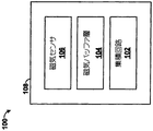
図1を参照すると、磁気検知システム100の例示的な一実施形態が示されている。図1では、磁気検知システム100を示しているが、他のパッケージおよび/またはセンサの組み合わせが同様に用いられてもよい。さらに、図1に示された磁気検知システム100および以下に記述される他の構成は、単なる例として記載され、製造上の必要性および/または消費者の嗜好性に応じて、他の構成と要素が代わりに用いられることができるし、また、ある要素は省略されてもよい。
Referring to FIG. 1, an exemplary embodiment of a
例として、磁気検知システム100は、集積回路102、磁気バッファ層104および磁気センサ106を有する。集積回路102、磁気バッファ層104および磁気センサ106は、プラスチックパッケージ、多数の出力ピンを有する電子集積回路パッケージ、または非磁性のモールド化パッケージなどのパッケージ108内部に、全部が封入されてよい。このパッケージはまた、銅のリードフレームを有する、スモールアウトライン集積回路(SOIC)パッケージであってもよい。また磁気検知システム100は、他の検知素子および/または電子素子を含んでもよい。
As an example, the
図1に示されているように、磁気バッファ層104は、集積回路102上に配置され、磁気センサ106は、磁気バッファ層104上に配置されている。磁気センサ106は、集積回路102と実質的に整列するように配置されていてもよいし、または磁気センサ106は、集積回路102の真上にくるように配置される。代替案として、磁気センサ106、磁気バッファ層104および集積回路102は、全く異なる構成で配置されていてもよい。しかしながら、例示的な実施形態としては、磁気バッファ層104を少なくとも磁気センサ106と集積回路102の間に配置することが必要である。
As shown in FIG. 1, the
磁気検知システム100の集積回路102は、プリント回路基板(PCB)、電子回路基板、集積回路チップ、または電気信号を処理することができる任意の回路であってよい。集積回路102は、シリコン材料片または相補型金属酸化膜半導体(CMOS)バイポーラ材料であってよい。集積回路102は、アナログおよびデジタル双方の出力を有してもよく、オペアンプ、増幅器または他の信号処理用の電子素子を含んでもよい。また集積回路102は同様に、他の型式の回路であってもよい。
The
電荷担体、即ち電子が集積回路102の導体(例えばトレース)内を移動すると、集積回路102により磁場が生成される。例えば、電流は、磁場を生成することができる。脈動する直流または交流は、特性的に電磁場を生成する。(一定の速度で移動するのではなく)荷電粒子が加速されると、変動する磁場が生成される。これは変動する電場を生成し、これがまた交互に他の変化する磁場を生成する。荷電粒子が加速され続けると、抑制されることなく成長し続ける成長する磁場に帰着する。
As charge carriers, or electrons, move through conductors (eg, traces) of
磁気バッファ層104は、集積回路102内部の電流により生成される電磁場から磁気センサ106を遮蔽し、および/または磁気バッファ層104は、集積回路102により生成される電磁場を吸収する。磁気バッファ層104はまた、磁気検知システム100の他の内部要因により生成される電磁場を遮蔽および/または吸収する。電磁場の吸収のために、磁気バッファ層104は、パーマロイ(商標)材料を含んでいてもよい。代替案として、電磁場の遮蔽のために、磁気バッファ層104は、ミューメタル(Mu−metal)材料を含んでいてもよい。しかしながら、磁気バッファ層104は、任意の透磁率の高い材料(即ち磁場の強さに対する高い磁束密度の比率)および/または任意の磁気抵抗材料を含んでいてもよい。
The
パーマロイ(商標)材料は、一般的に、ニッケルと鉄を含んでいる。ある実施形態では磁気バッファ層104は、約60〜80%のニッケル(Ni)、10〜20%の鉄(Fe)、5〜10%の銅(Cu)および5〜10%のコバルト(Co)(重量%)のパーマロイ(商標)材料組成物からなる。パーマロイ(商標)組成物はまた、50〜80%のニッケルと残余鉄からなっていてもよい。
Permalloy ™ materials typically include nickel and iron. In some embodiments, the
ミューメタルは、軟磁性の強磁性体である。例としては、磁気バッファ層104は、約77%のNi、16%のFe、5%のCuおよび2%のクロム(Cr)のミューメタルであってもよい。例えば、ある量のシリコン(Si)および/または他の同様の元素が添加されたNi−Feベースの金属のような、他のミューメタル材料が用いられてもよい。他の元素が、同様に用いられてもよい。
Mumetal is a soft magnetic ferromagnet. As an example, the
磁気バッファ層104は、例えば104H/m(ヘンリーパーメートル)のオーダーのような高い透磁率を有する、任意の強磁性材料であってもよい。他の例を、同様に用いることができる。
The
磁気バッファ層104は、約数百オングストロームの厚さであってよいが、しかしながらその厚みはまた、数百オングストローム以上または以下であってもよい。例えば地球の磁場の測定用に設計された磁気検知システムのためには、磁気バッファ層104は、約100〜500オングストロームであってもよい。
The
磁気バッファ層104は、例えば加圧気相堆積法(PVD)またはイオンビーム蒸着法などの、電着のプロセスにより集積回路102の整合面上に堆積される。代替案として、磁気バッファ層104は、化学成長法(CVD)、常圧化学気相成長法(APCVD)、低圧化学気相成長法(LPCVD)、プラズマ化学気相成長法(PECVD)または他の薄膜形成技術により集積回路102の整合面上に堆積されてもよい。磁気バッファ層104は、迷走電流もしくは漏れ電流および/または磁場を削減および/または除去するために、集積回路102と磁気センサ106の間の領域にのみ、またはできるならば集積回路102よりも広い領域に、堆積されてもよい。例えば、磁気バッファ層104は、集積回路102と磁気センサ106の間の領域で定義される、または集積回路102の全表面で定義される、集積回路102の全整合面上に堆積される。
The
磁気バッファ層104は、磁気センサ106が磁場の強度または磁場の方向を、正確に測定することができるようにする。例えば磁気センサ106は、一般的に約0.5から0.6ガウスまたは約5×10⁻⁵テスラである、地球の磁場のような微弱な磁場を極めて正確に測定する。
The
一実施形態では磁気センサ106は、81%Niおよび19%Feのような、異方性磁気抵抗(AMR)膜材料の薄層である。AMR膜は、磁場に曝されるとその抵抗を2〜3%変化させる。他の実施形態では、磁気センサ106は、Ni−Fe−CU−Ni−Feの積層または他の組み合わせを有し、磁場に曝されるとその抵抗を3〜100%変化させる、巨大磁気抵抗(GMR)膜材料である。さらに他の実施形態では磁気センサ106は、ランタン(La)、ストロンチウム(Sr)、マンガン(Mn)および酸素(O)からなる、超巨大磁気抵抗(CMR)膜材料である。磁気センサ106は、他の材料を同様に含んでもよい。
In one embodiment, the
一実施形態では、磁気センサ106は、約200オングストロームより小さい厚みを有する。磁気センサ106を構成する膜材料の層は、磁気バッファ層104の上に堆積され、磁気センサ106の望ましい形成物は、膜材料の層内にエッチングされる。磁気センサ106は、PVDまたはイオンビーム堆積法を用いて、磁気バッファ層104の上に堆積される。
In one embodiment, the
磁気センサ106は、磁気抵抗金属膜により形成された、抵抗性ホイートストンブリッジを含んでいる。ブリッジに電源装置が接続されると、磁気センサ106は高感度方向の自然環境の磁場または印加された磁場を、電圧の出力に変換する。
The
磁気バッファ層104は、磁気センサ106が集積回路102の真上にくるようにまたは極めて近接して備えられながら、磁場を敏感に検出する能力を維持することを可能にする。さらに磁気バッファ層104は、集積回路102により生成される磁場が磁気検知システム100の外部の電磁場を妨害しないようにする。磁気センサ106と集積回路102の間の電磁場の遮蔽層または吸収層がなければ、集積回路102内部の電流により生成される電磁場は磁気センサ106を飽和させることができ、磁気センサ106が磁気検知システム100の外部の電磁場を検出することを不可能にする。
The
図2を参照すると、図1に示された磁気検知システム100の詳細な図が描かれている。集積回路102は、パッケージ108の基板に備えられ、磁気バッファ層104は、集積回路102上に堆積されている。第1の金属導線202(a−b)が、磁気バッファ層104を覆って集積回路102に堆積されている。誘電体層204が、磁気バッファ層104を覆って集積回路102と第1の金属導線202(a−b)のまわりに堆積されている。磁気センサ106は、誘電体層204上に堆積され、望ましい形状になるようにエッチングされる。例えば図2に示されているように、磁気センサ106は、3つの小さい平行な部分からなる。第2の金属導線206が、磁気センサ106上に堆積され、第1の金属導線202(a−b)と接触するようになっている。
Referring to FIG. 2, a detailed view of the
他の誘電体層208が、誘電体層204と第2の金属導線206の上に堆積されている。第3の金属導線210が、誘電体層208の上に堆積され、第2の金属導線206と接触するようになっている。他の誘電体層212が、第3の金属導線210の上に堆積され、出力用の金属導線214(a−b)が、誘電体層212上に堆積され、出力用の金属導線214(a−b)が、第3の金属導線210と接触するようになっている。
Another
この磁気検知システム100に含まれて記述された、多数の誘電体層と金属導線(およびその組成と各々の厚み)は、本発明の全ての実施形態には本質的なことではなく、他の構成も同様に本発明の利点を発揮する。同様に、本発明に記載された構成、即ちパッケージ化された集積回路の構成は、単なる採用されてもよい多くの異なる形態の1例である。
The multiple dielectric layers and metal conductors (and their composition and thickness) described and included in this
誘電体層204、208、212は、テトラエチルオルソシリケート(TEOS)材料または他の絶縁材料および/または非伝導性材料からなる。さらに誘電体層204、208、212は、厚みが約1〜2ミクロンであってよい。誘電体層204、208、212が堆積される表面を滑らかかつ平坦にしておよび/または表面の不完全度を除去するために、誘電体層204、208、212を堆積するのに先だって、化学的機械的研磨(CMP)プロセスが完了される。誘電体層204、208、212は、PECVD法で堆積される。
The
図3を参照すると、磁気検知装置を内部的に遮蔽する方法300が示されている。ブロック302に示されているように、その上に磁気抵抗材料の層が堆積される、集積回路の表面が清浄化される。次に、ブロック304に示されているように、磁気抵抗材料の層は集積回路の上に堆積され、ブロック306に示されているように材料の誘電体層が磁気抵抗層の上に堆積される。ブロック308に示されているように、材料の磁気検知層が誘電体層の上に堆積され、ブロック310に示されているように、集積回路および磁気センサはパッケージ化される。集積回路により生成される電磁信号を吸収するために、磁気抵抗材料の層が磁気検知層と集積回路の間に堆積される。
Referring to FIG. 3, a
磁気センサと集積回路の間に磁気抵抗材料を組み込むことは、検知システム内部の発生源により生成される磁場による、磁場測定の誤検出を補償する必要性を除去する。さらに、現存する磁気検知システムでは、交流により生成されるような時間的に変化する磁場を補償することは不可能である。それ故、磁気遮蔽層または磁気吸収層として磁気抵抗材料を使用することは、装置外の磁場の特性を正確に測定するための、磁気センサと集積回路を有する統合された磁気検知装置を可能にする。 Incorporating a magnetoresistive material between the magnetic sensor and the integrated circuit eliminates the need to compensate for false detection of magnetic field measurements due to the magnetic field generated by a source inside the sensing system. Furthermore, existing magnetic sensing systems cannot compensate for time-varying magnetic fields such as those generated by alternating current. Therefore, the use of a magnetoresistive material as a magnetic shielding layer or magnetic absorption layer allows an integrated magnetic sensing device with a magnetic sensor and integrated circuit to accurately measure the characteristics of the magnetic field outside the device. To do.
本発明が関係する技術の当業者は、本発明の精神または特性から逸脱することなく、その原理を用いて他の実施形態に帰着する変形を行うことができる。従って、以上に記載された実施形態は、あらゆる点で単なる例であって限定的なものではないと見なされるべきであり、そのため本発明の権利範囲は、上記の記述ではなくむしろ添付の請求項により示される。結果として、構成、順序、材料その他の当業者には自明の変形は、本発明の権利範囲に属する。他の実施形態が、同様に可能である。 Those skilled in the art to which the present invention pertains can make variations that result in other embodiments using its principles without departing from the spirit or characteristics of the present invention. Accordingly, the embodiments described above are to be considered in all respects only as illustrative and not restrictive, so the scope of the present invention is not the above description but rather the appended claims. Indicated by. As a result, configurations, sequences, materials, and other modifications obvious to those skilled in the art are within the scope of the present invention. Other embodiments are possible as well.
Claims (23)
前記整合面上に堆積された磁気遮蔽層であって、前記集積回路により生成される電磁信号を吸収する磁気遮蔽層と、
前記集積回路と実質的に整列するように、前記磁気遮蔽層上に堆積された磁気検知層と、
を含む磁気検知装置。 An integrated circuit having a matching surface;
A magnetic shielding layer deposited on the matching surface for absorbing electromagnetic signals generated by the integrated circuit;
A magnetic sensing layer deposited on the magnetic shielding layer so as to be substantially aligned with the integrated circuit;
Magnetic sensing device including
さらに含む請求項1に記載の磁気検知装置。 A dielectric layer deposited between the integrated circuit and the magnetic sensing layer;
The magnetic detection device according to claim 1, further comprising:
前記集積回路と組み合わせられた磁気センサと、
前記集積回路と前記磁気検知層の間に堆積された磁気バッファ層であって、約100〜500オングストロームの厚みを有する磁気遮蔽材料を含む磁気バッファ層と、
を含む磁気検知装置。 An integrated circuit having a matching surface;
A magnetic sensor combined with the integrated circuit;
A magnetic buffer layer deposited between the integrated circuit and the magnetic sensing layer, the magnetic buffer layer comprising a magnetic shielding material having a thickness of about 100 to 500 Angstroms;
Magnetic sensing device including
さらに含む請求項9に記載の磁気検知装置。 A dielectric layer deposited between the integrated circuit and the magnetic sensor;
The magnetic detection device according to claim 9, further comprising:
さらに含む請求項16に記載の方法。 Integrating the magnetic sensor and the integrated circuit into a common magnetic sensing device;
The method of claim 16 further comprising:
さらに含む請求項16に記載の方法。 Depositing an insulating layer between the magnetic sensor and the integrated circuit;
The method of claim 16 further comprising:
Applications Claiming Priority (2)
| Application Number | Priority Date | Filing Date | Title |
|---|---|---|---|
| US10/201,381 US7037604B2 (en) | 2002-07-23 | 2002-07-23 | Magnetic sensing device |
| PCT/US2003/023389 WO2004015437A1 (en) | 2002-07-23 | 2003-07-23 | Magnetic sensing device |
Publications (2)
| Publication Number | Publication Date |
|---|---|
| JP2005534193A true JP2005534193A (en) | 2005-11-10 |
| JP2005534193A5 JP2005534193A5 (en) | 2006-09-14 |
Family
ID=30769637
Family Applications (1)
| Application Number | Title | Priority Date | Filing Date |
|---|---|---|---|
| JP2004527657A Withdrawn JP2005534193A (en) | 2002-07-23 | 2003-07-23 | Magnetic detector |
Country Status (8)
| Country | Link |
|---|---|
| US (1) | US7037604B2 (en) |
| EP (1) | EP1540362B1 (en) |
| JP (1) | JP2005534193A (en) |
| CN (1) | CN1672058A (en) |
| AU (1) | AU2003265301A1 (en) |
| CA (1) | CA2493438A1 (en) |
| DE (1) | DE60327781D1 (en) |
| WO (1) | WO2004015437A1 (en) |
Cited By (1)
| Publication number | Priority date | Publication date | Assignee | Title |
|---|---|---|---|---|
| JP2007106401A (en) * | 2005-10-10 | 2007-04-26 | Infineon Technologies Sensonor As | Tire air pressure monitoring system, tire module and receiver |
Families Citing this family (25)
| Publication number | Priority date | Publication date | Assignee | Title |
|---|---|---|---|---|
| US20040037818A1 (en) * | 1998-07-30 | 2004-02-26 | Brand Stephen J. | Treatment for diabetes |
| US7239000B2 (en) * | 2003-04-15 | 2007-07-03 | Honeywell International Inc. | Semiconductor device and magneto-resistive sensor integration |
| US6883241B2 (en) * | 2003-07-31 | 2005-04-26 | Medtronic, Inc. | Compass-based indicator with magnetic shielding |
| US7126330B2 (en) * | 2004-06-03 | 2006-10-24 | Honeywell International, Inc. | Integrated three-dimensional magnetic sensing device and method to fabricate an integrated three-dimensional magnetic sensing device |
| KR20060021649A (en) * | 2004-09-03 | 2006-03-08 | 엘지전자 주식회사 | Magnetic sensor for detection of short leading wire position having high density detailed pattern |
| US7064558B1 (en) * | 2004-12-16 | 2006-06-20 | Honeywell International Inc. | Millivolt output circuit for use with programmable sensor compensation integrated circuits |
| DE102005047414B4 (en) * | 2005-02-21 | 2012-01-05 | Infineon Technologies Ag | Magnetoresistive sensor module and method for producing the same |
| US7545662B2 (en) * | 2005-03-25 | 2009-06-09 | Taiwan Semiconductor Manufacturing Co., Ltd. | Method and system for magnetic shielding in semiconductor integrated circuit |
| TWI295102B (en) * | 2006-01-13 | 2008-03-21 | Ind Tech Res Inst | Multi-functional substrate structure |
| SG135077A1 (en) * | 2006-02-27 | 2007-09-28 | Nanyang Polytechnic | Apparatus and method for non-invasively sensing pulse rate and blood flow anomalies |
| BRPI0605714B1 (en) * | 2006-03-07 | 2018-06-26 | José Gouveia Abrunhosa Jorge | DEVICE AND PROCESS FOR DETECTION OF MAGNETIC MATERIALS IN ELECTROMAGNETIC TECHNOLOGY ANTI-THEFT SYSTEMS |
| EP2360489B1 (en) * | 2010-02-04 | 2013-04-17 | Nxp B.V. | Magnetic field sensor |
| TWI443360B (en) * | 2011-02-22 | 2014-07-01 | Voltafield Technology Corp | Magnetic sensor and fabricating method thereof |
| TWI467821B (en) * | 2010-12-31 | 2015-01-01 | Voltafield Technology Corp | Magnetic sensor and fabricating method thereof |
| US20140347047A1 (en) * | 2011-02-22 | 2014-11-27 | Voltafield Technology Corporation | Magnetoresistive sensor |
| ITTO20120614A1 (en) * | 2012-07-11 | 2014-01-12 | St Microelectronics Srl | MULTILAYER INTEGRATED MAGNETORESISTIVE SENSOR AND ITS MANUFACTURING METHOD |
| JP5876583B2 (en) * | 2013-03-26 | 2016-03-02 | 旭化成エレクトロニクス株式会社 | Magnetic sensor and magnetic detection method thereof |
| DE202013003631U1 (en) * | 2013-04-18 | 2013-04-26 | Steiner-Optik Gmbh | Batteriefachschirmung |
| US10180341B2 (en) * | 2013-10-24 | 2019-01-15 | The United States Of America As Represented By The Administrator Of Nasa | Multi-layer wireless sensor construct for use at electrically-conductive material surfaces |
| US10193228B2 (en) | 2013-10-24 | 2019-01-29 | The United States Of America As Represented By The Administrator Of Nasa | Antenna for near field sensing and far field transceiving |
| US9497846B2 (en) | 2013-10-24 | 2016-11-15 | The United States Of America As Represented By The Administrator Of The National Aeronautics And Space Administration | Plasma generator using spiral conductors |
| CN103647022B (en) * | 2013-12-25 | 2016-04-27 | 杭州士兰集成电路有限公司 | Anisotropic magneto resistive sensor vertical structure and manufacture method thereof |
| US10145906B2 (en) | 2015-12-17 | 2018-12-04 | Analog Devices Global | Devices, systems and methods including magnetic structures |
| CN106229406A (en) * | 2016-10-10 | 2016-12-14 | 杭州士兰集成电路有限公司 | Integrated-type magnetic switch and manufacture method thereof |
| US10591320B2 (en) * | 2017-12-11 | 2020-03-17 | Nxp B.V. | Magnetoresistive sensor with stray field cancellation and systems incorporating same |
Family Cites Families (20)
| Publication number | Priority date | Publication date | Assignee | Title |
|---|---|---|---|---|
| US5041780A (en) | 1988-09-13 | 1991-08-20 | California Institute Of Technology | Integrable current sensors |
| JPH02129882U (en) | 1989-03-31 | 1990-10-25 | ||
| US5247278A (en) * | 1991-11-26 | 1993-09-21 | Honeywell Inc. | Magnetic field sensing device |
| US5570015A (en) | 1992-02-05 | 1996-10-29 | Mitsubishi Denki Kabushiki Kaisha | Linear positional displacement detector for detecting linear displacement of a permanent magnet as a change in direction of magnetic sensor unit |
| US5757591A (en) * | 1996-11-25 | 1998-05-26 | International Business Machines Corporation | Magnetoresistive read/inductive write magnetic head assembly fabricated with silicon on hard insulator for improved durability and electrostatic discharge protection and method for manufacturing same |
| US5902690A (en) * | 1997-02-25 | 1999-05-11 | Motorola, Inc. | Stray magnetic shielding for a non-volatile MRAM |
| US5898548A (en) * | 1997-10-24 | 1999-04-27 | International Business Machines Corporation | Shielded magnetic tunnel junction magnetoresistive read head |
| JPH11154309A (en) * | 1997-11-20 | 1999-06-08 | Sony Corp | Magneto-resistive effect magnetic head |
| US6048739A (en) * | 1997-12-18 | 2000-04-11 | Honeywell Inc. | Method of manufacturing a high density magnetic memory device |
| US6072382A (en) * | 1998-01-06 | 2000-06-06 | Nonvolatile Electronics, Incorporated | Spin dependent tunneling sensor |
| GB2370912A (en) | 1999-10-05 | 2002-07-10 | Seagate Technology Llc | Integrated on-board device and method for the protection of magnetoresistive heads from electrostatic discharge |
| US6462541B1 (en) | 1999-11-12 | 2002-10-08 | Nve Corporation | Uniform sense condition magnetic field sensor using differential magnetoresistance |
| WO2001071713A1 (en) * | 2000-03-22 | 2001-09-27 | Nve Corporation | Read heads in planar monolithic integrated circuit chips |
| US6452253B1 (en) * | 2000-08-31 | 2002-09-17 | Micron Technology, Inc. | Method and apparatus for magnetic shielding of an integrated circuit |
| US6717241B1 (en) * | 2000-08-31 | 2004-04-06 | Micron Technology, Inc. | Magnetic shielding for integrated circuits |
| US6515352B1 (en) * | 2000-09-25 | 2003-02-04 | Micron Technology, Inc. | Shielding arrangement to protect a circuit from stray magnetic fields |
| JP3659898B2 (en) * | 2000-11-27 | 2005-06-15 | Tdk株式会社 | Thin film magnetic head and manufacturing method thereof |
| JP2002184945A (en) * | 2000-12-11 | 2002-06-28 | Fuji Electric Co Ltd | Semiconductor device integrated with magnetic element |
| US6724027B2 (en) * | 2002-04-18 | 2004-04-20 | Hewlett-Packard Development Company, L.P. | Magnetic shielding for MRAM devices |
| US6936763B2 (en) * | 2002-06-28 | 2005-08-30 | Freescale Semiconductor, Inc. | Magnetic shielding for electronic circuits which include magnetic materials |
-
2002
- 2002-07-23 US US10/201,381 patent/US7037604B2/en not_active Expired - Fee Related
-
2003
- 2003-07-23 JP JP2004527657A patent/JP2005534193A/en not_active Withdrawn
- 2003-07-23 EP EP03784822A patent/EP1540362B1/en not_active Expired - Lifetime
- 2003-07-23 WO PCT/US2003/023389 patent/WO2004015437A1/en active Application Filing
- 2003-07-23 AU AU2003265301A patent/AU2003265301A1/en not_active Abandoned
- 2003-07-23 CN CNA038175053A patent/CN1672058A/en active Pending
- 2003-07-23 DE DE60327781T patent/DE60327781D1/en not_active Expired - Fee Related
- 2003-07-23 CA CA002493438A patent/CA2493438A1/en not_active Abandoned
Cited By (1)
| Publication number | Priority date | Publication date | Assignee | Title |
|---|---|---|---|---|
| JP2007106401A (en) * | 2005-10-10 | 2007-04-26 | Infineon Technologies Sensonor As | Tire air pressure monitoring system, tire module and receiver |
Also Published As
| Publication number | Publication date |
|---|---|
| EP1540362A1 (en) | 2005-06-15 |
| DE60327781D1 (en) | 2009-07-09 |
| WO2004015437A1 (en) | 2004-02-19 |
| US7037604B2 (en) | 2006-05-02 |
| EP1540362B1 (en) | 2009-05-27 |
| US20040019272A1 (en) | 2004-01-29 |
| CA2493438A1 (en) | 2004-02-19 |
| CN1672058A (en) | 2005-09-21 |
| AU2003265301A1 (en) | 2004-02-25 |
Similar Documents
| Publication | Publication Date | Title |
|---|---|---|
| EP1540362B1 (en) | Magnetic sensing device | |
| EP1720027B1 (en) | Magnetic field detector and current detection device, position detection device and rotation detection device using the magnetic field detector | |
| JP4105142B2 (en) | Current sensor | |
| CN103954920B (en) | A kind of single-chip tri-axis linear magnetic sensor and preparation method thereof | |
| US8519704B2 (en) | Magnetic-balance-system current sensor | |
| JP4105147B2 (en) | Current sensor | |
| CN103149542B (en) | Under second-harmonic detection pattern, use magnetoresistive transducer to sense the method for low-intensity magnetic field | |
| JP4508058B2 (en) | Magnetic field detection device and manufacturing method thereof | |
| CN103901363A (en) | Single-chip Z-axis linear magneto-resistive sensor | |
| US20060012459A1 (en) | Sensor and method for measuring a current of charged particles | |
| CN110231494A (en) | Magnetic speed sensor with distributed Wheatstone bridge | |
| CN104656045A (en) | Magnetic field sensing module, measuring method and manufacturing method of magnetic field sensing module | |
| CN109633505A (en) | Magnetic Sensor sensitivity matching calibration | |
| KR19990022160A (en) | Magnetic field sensor including bridge circuit of magnetoresistive bridge element | |
| CN203480009U (en) | Single-chip Z-axis linear magneto-resistor sensor | |
| JP6132085B2 (en) | Magnetic detector | |
| JP4741152B2 (en) | Apparatus for measuring magnetic field and method for producing apparatus for measuring magnetic field | |
| EP0910802A2 (en) | Magnetic field sensor comprising a wheatstone bridge | |
| US11002806B2 (en) | Magnetic field detection device | |
| CN210572104U (en) | Hydrogen sensor based on electric isolation tunnel magnetic resistance sensitive element | |
| JP7232647B2 (en) | Magnetic detector | |
| JP2013047610A (en) | Magnetic balance type current sensor | |
| KR20050019925A (en) | Magnetic sensing device | |
| US20230066358A1 (en) | Strayfield insensitive magnetic sensing device and method using spin orbit torque effect | |
| TW202246781A (en) | Electric current sensor and sensing device |
Legal Events
| Date | Code | Title | Description |
|---|---|---|---|
| A521 | Written amendment |
Free format text: JAPANESE INTERMEDIATE CODE: A523 Effective date: 20060724 |
|
| A621 | Written request for application examination |
Free format text: JAPANESE INTERMEDIATE CODE: A621 Effective date: 20060724 |
|
| A761 | Written withdrawal of application |
Free format text: JAPANESE INTERMEDIATE CODE: A761 Effective date: 20090611 |