JP2005533331A - Multi-stack optical data storage medium and use of the medium - Google Patents
Multi-stack optical data storage medium and use of the medium Download PDFInfo
- Publication number
- JP2005533331A JP2005533331A JP2004520983A JP2004520983A JP2005533331A JP 2005533331 A JP2005533331 A JP 2005533331A JP 2004520983 A JP2004520983 A JP 2004520983A JP 2004520983 A JP2004520983 A JP 2004520983A JP 2005533331 A JP2005533331 A JP 2005533331A
- Authority
- JP
- Japan
- Prior art keywords
- recording
- layer
- stack
- storage medium
- thickness
- Prior art date
- Legal status (The legal status is an assumption and is not a legal conclusion. Google has not performed a legal analysis and makes no representation as to the accuracy of the status listed.)
- Withdrawn
Links
Images


Classifications
-
- G—PHYSICS
- G11—INFORMATION STORAGE
- G11B—INFORMATION STORAGE BASED ON RELATIVE MOVEMENT BETWEEN RECORD CARRIER AND TRANSDUCER
- G11B7/00—Recording or reproducing by optical means, e.g. recording using a thermal beam of optical radiation by modifying optical properties or the physical structure, reproducing using an optical beam at lower power by sensing optical properties; Record carriers therefor
- G11B7/24—Record carriers characterised by shape, structure or physical properties, or by the selection of the material
- G11B7/241—Record carriers characterised by shape, structure or physical properties, or by the selection of the material characterised by the selection of the material
- G11B7/242—Record carriers characterised by shape, structure or physical properties, or by the selection of the material characterised by the selection of the material of recording layers
- G11B7/243—Record carriers characterised by shape, structure or physical properties, or by the selection of the material characterised by the selection of the material of recording layers comprising inorganic materials only, e.g. ablative layers
-
- G—PHYSICS
- G11—INFORMATION STORAGE
- G11B—INFORMATION STORAGE BASED ON RELATIVE MOVEMENT BETWEEN RECORD CARRIER AND TRANSDUCER
- G11B7/00—Recording or reproducing by optical means, e.g. recording using a thermal beam of optical radiation by modifying optical properties or the physical structure, reproducing using an optical beam at lower power by sensing optical properties; Record carriers therefor
- G11B7/004—Recording, reproducing or erasing methods; Read, write or erase circuits therefor
- G11B7/005—Reproducing
- G11B7/0051—Reproducing involving phase depth effects
-
- G—PHYSICS
- G11—INFORMATION STORAGE
- G11B—INFORMATION STORAGE BASED ON RELATIVE MOVEMENT BETWEEN RECORD CARRIER AND TRANSDUCER
- G11B7/00—Recording or reproducing by optical means, e.g. recording using a thermal beam of optical radiation by modifying optical properties or the physical structure, reproducing using an optical beam at lower power by sensing optical properties; Record carriers therefor
- G11B7/24—Record carriers characterised by shape, structure or physical properties, or by the selection of the material
- G11B7/2403—Layers; Shape, structure or physical properties thereof
- G11B7/24035—Recording layers
- G11B7/24038—Multiple laminated recording layers
-
- G—PHYSICS
- G11—INFORMATION STORAGE
- G11B—INFORMATION STORAGE BASED ON RELATIVE MOVEMENT BETWEEN RECORD CARRIER AND TRANSDUCER
- G11B7/00—Recording or reproducing by optical means, e.g. recording using a thermal beam of optical radiation by modifying optical properties or the physical structure, reproducing using an optical beam at lower power by sensing optical properties; Record carriers therefor
- G11B7/24—Record carriers characterised by shape, structure or physical properties, or by the selection of the material
- G11B7/2403—Layers; Shape, structure or physical properties thereof
- G11B7/24067—Combinations of two or more layers with specific interrelation
-
- G—PHYSICS
- G11—INFORMATION STORAGE
- G11B—INFORMATION STORAGE BASED ON RELATIVE MOVEMENT BETWEEN RECORD CARRIER AND TRANSDUCER
- G11B7/00—Recording or reproducing by optical means, e.g. recording using a thermal beam of optical radiation by modifying optical properties or the physical structure, reproducing using an optical beam at lower power by sensing optical properties; Record carriers therefor
- G11B7/24—Record carriers characterised by shape, structure or physical properties, or by the selection of the material
- G11B7/241—Record carriers characterised by shape, structure or physical properties, or by the selection of the material characterised by the selection of the material
- G11B7/242—Record carriers characterised by shape, structure or physical properties, or by the selection of the material characterised by the selection of the material of recording layers
- G11B7/243—Record carriers characterised by shape, structure or physical properties, or by the selection of the material characterised by the selection of the material of recording layers comprising inorganic materials only, e.g. ablative layers
- G11B7/2433—Metals or elements of groups 13, 14, 15 or 16 of the Periodic System, e.g. B, Si, Ge, As, Sb, Bi, Se or Te
-
- G—PHYSICS
- G11—INFORMATION STORAGE
- G11B—INFORMATION STORAGE BASED ON RELATIVE MOVEMENT BETWEEN RECORD CARRIER AND TRANSDUCER
- G11B7/00—Recording or reproducing by optical means, e.g. recording using a thermal beam of optical radiation by modifying optical properties or the physical structure, reproducing using an optical beam at lower power by sensing optical properties; Record carriers therefor
- G11B7/24—Record carriers characterised by shape, structure or physical properties, or by the selection of the material
- G11B7/241—Record carriers characterised by shape, structure or physical properties, or by the selection of the material characterised by the selection of the material
- G11B7/252—Record carriers characterised by shape, structure or physical properties, or by the selection of the material characterised by the selection of the material of layers other than recording layers
- G11B7/257—Record carriers characterised by shape, structure or physical properties, or by the selection of the material characterised by the selection of the material of layers other than recording layers of layers having properties involved in recording or reproduction, e.g. optical interference layers or sensitising layers or dielectric layers, which are protecting the recording layers
-
- G—PHYSICS
- G11—INFORMATION STORAGE
- G11B—INFORMATION STORAGE BASED ON RELATIVE MOVEMENT BETWEEN RECORD CARRIER AND TRANSDUCER
- G11B7/00—Recording or reproducing by optical means, e.g. recording using a thermal beam of optical radiation by modifying optical properties or the physical structure, reproducing using an optical beam at lower power by sensing optical properties; Record carriers therefor
- G11B7/24—Record carriers characterised by shape, structure or physical properties, or by the selection of the material
- G11B7/241—Record carriers characterised by shape, structure or physical properties, or by the selection of the material characterised by the selection of the material
- G11B7/242—Record carriers characterised by shape, structure or physical properties, or by the selection of the material characterised by the selection of the material of recording layers
- G11B7/243—Record carriers characterised by shape, structure or physical properties, or by the selection of the material characterised by the selection of the material of recording layers comprising inorganic materials only, e.g. ablative layers
- G11B2007/24302—Metals or metalloids
- G11B2007/24312—Metals or metalloids group 14 elements (e.g. Si, Ge, Sn)
-
- G—PHYSICS
- G11—INFORMATION STORAGE
- G11B—INFORMATION STORAGE BASED ON RELATIVE MOVEMENT BETWEEN RECORD CARRIER AND TRANSDUCER
- G11B7/00—Recording or reproducing by optical means, e.g. recording using a thermal beam of optical radiation by modifying optical properties or the physical structure, reproducing using an optical beam at lower power by sensing optical properties; Record carriers therefor
- G11B7/24—Record carriers characterised by shape, structure or physical properties, or by the selection of the material
- G11B7/241—Record carriers characterised by shape, structure or physical properties, or by the selection of the material characterised by the selection of the material
- G11B7/242—Record carriers characterised by shape, structure or physical properties, or by the selection of the material characterised by the selection of the material of recording layers
- G11B7/243—Record carriers characterised by shape, structure or physical properties, or by the selection of the material characterised by the selection of the material of recording layers comprising inorganic materials only, e.g. ablative layers
- G11B2007/24302—Metals or metalloids
- G11B2007/24314—Metals or metalloids group 15 elements (e.g. Sb, Bi)
-
- G—PHYSICS
- G11—INFORMATION STORAGE
- G11B—INFORMATION STORAGE BASED ON RELATIVE MOVEMENT BETWEEN RECORD CARRIER AND TRANSDUCER
- G11B7/00—Recording or reproducing by optical means, e.g. recording using a thermal beam of optical radiation by modifying optical properties or the physical structure, reproducing using an optical beam at lower power by sensing optical properties; Record carriers therefor
- G11B7/24—Record carriers characterised by shape, structure or physical properties, or by the selection of the material
- G11B7/241—Record carriers characterised by shape, structure or physical properties, or by the selection of the material characterised by the selection of the material
- G11B7/242—Record carriers characterised by shape, structure or physical properties, or by the selection of the material characterised by the selection of the material of recording layers
- G11B7/243—Record carriers characterised by shape, structure or physical properties, or by the selection of the material characterised by the selection of the material of recording layers comprising inorganic materials only, e.g. ablative layers
- G11B2007/24302—Metals or metalloids
- G11B2007/24316—Metals or metalloids group 16 elements (i.e. chalcogenides, Se, Te)
-
- G—PHYSICS
- G11—INFORMATION STORAGE
- G11B—INFORMATION STORAGE BASED ON RELATIVE MOVEMENT BETWEEN RECORD CARRIER AND TRANSDUCER
- G11B7/00—Recording or reproducing by optical means, e.g. recording using a thermal beam of optical radiation by modifying optical properties or the physical structure, reproducing using an optical beam at lower power by sensing optical properties; Record carriers therefor
- G11B7/24—Record carriers characterised by shape, structure or physical properties, or by the selection of the material
- G11B7/241—Record carriers characterised by shape, structure or physical properties, or by the selection of the material characterised by the selection of the material
- G11B7/252—Record carriers characterised by shape, structure or physical properties, or by the selection of the material characterised by the selection of the material of layers other than recording layers
- G11B7/257—Record carriers characterised by shape, structure or physical properties, or by the selection of the material characterised by the selection of the material of layers other than recording layers of layers having properties involved in recording or reproduction, e.g. optical interference layers or sensitising layers or dielectric layers, which are protecting the recording layers
- G11B2007/25705—Record carriers characterised by shape, structure or physical properties, or by the selection of the material characterised by the selection of the material of layers other than recording layers of layers having properties involved in recording or reproduction, e.g. optical interference layers or sensitising layers or dielectric layers, which are protecting the recording layers consisting essentially of inorganic materials
- G11B2007/25706—Record carriers characterised by shape, structure or physical properties, or by the selection of the material characterised by the selection of the material of layers other than recording layers of layers having properties involved in recording or reproduction, e.g. optical interference layers or sensitising layers or dielectric layers, which are protecting the recording layers consisting essentially of inorganic materials containing transition metal elements (Zn, Fe, Co, Ni, Pt)
-
- G—PHYSICS
- G11—INFORMATION STORAGE
- G11B—INFORMATION STORAGE BASED ON RELATIVE MOVEMENT BETWEEN RECORD CARRIER AND TRANSDUCER
- G11B7/00—Recording or reproducing by optical means, e.g. recording using a thermal beam of optical radiation by modifying optical properties or the physical structure, reproducing using an optical beam at lower power by sensing optical properties; Record carriers therefor
- G11B7/24—Record carriers characterised by shape, structure or physical properties, or by the selection of the material
- G11B7/241—Record carriers characterised by shape, structure or physical properties, or by the selection of the material characterised by the selection of the material
- G11B7/252—Record carriers characterised by shape, structure or physical properties, or by the selection of the material characterised by the selection of the material of layers other than recording layers
- G11B7/257—Record carriers characterised by shape, structure or physical properties, or by the selection of the material characterised by the selection of the material of layers other than recording layers of layers having properties involved in recording or reproduction, e.g. optical interference layers or sensitising layers or dielectric layers, which are protecting the recording layers
- G11B2007/25705—Record carriers characterised by shape, structure or physical properties, or by the selection of the material characterised by the selection of the material of layers other than recording layers of layers having properties involved in recording or reproduction, e.g. optical interference layers or sensitising layers or dielectric layers, which are protecting the recording layers consisting essentially of inorganic materials
- G11B2007/25708—Record carriers characterised by shape, structure or physical properties, or by the selection of the material characterised by the selection of the material of layers other than recording layers of layers having properties involved in recording or reproduction, e.g. optical interference layers or sensitising layers or dielectric layers, which are protecting the recording layers consisting essentially of inorganic materials containing group 13 elements (B, Al, Ga)
-
- G—PHYSICS
- G11—INFORMATION STORAGE
- G11B—INFORMATION STORAGE BASED ON RELATIVE MOVEMENT BETWEEN RECORD CARRIER AND TRANSDUCER
- G11B7/00—Recording or reproducing by optical means, e.g. recording using a thermal beam of optical radiation by modifying optical properties or the physical structure, reproducing using an optical beam at lower power by sensing optical properties; Record carriers therefor
- G11B7/24—Record carriers characterised by shape, structure or physical properties, or by the selection of the material
- G11B7/241—Record carriers characterised by shape, structure or physical properties, or by the selection of the material characterised by the selection of the material
- G11B7/252—Record carriers characterised by shape, structure or physical properties, or by the selection of the material characterised by the selection of the material of layers other than recording layers
- G11B7/257—Record carriers characterised by shape, structure or physical properties, or by the selection of the material characterised by the selection of the material of layers other than recording layers of layers having properties involved in recording or reproduction, e.g. optical interference layers or sensitising layers or dielectric layers, which are protecting the recording layers
- G11B2007/25705—Record carriers characterised by shape, structure or physical properties, or by the selection of the material characterised by the selection of the material of layers other than recording layers of layers having properties involved in recording or reproduction, e.g. optical interference layers or sensitising layers or dielectric layers, which are protecting the recording layers consisting essentially of inorganic materials
- G11B2007/25713—Record carriers characterised by shape, structure or physical properties, or by the selection of the material characterised by the selection of the material of layers other than recording layers of layers having properties involved in recording or reproduction, e.g. optical interference layers or sensitising layers or dielectric layers, which are protecting the recording layers consisting essentially of inorganic materials containing nitrogen
-
- G—PHYSICS
- G11—INFORMATION STORAGE
- G11B—INFORMATION STORAGE BASED ON RELATIVE MOVEMENT BETWEEN RECORD CARRIER AND TRANSDUCER
- G11B7/00—Recording or reproducing by optical means, e.g. recording using a thermal beam of optical radiation by modifying optical properties or the physical structure, reproducing using an optical beam at lower power by sensing optical properties; Record carriers therefor
- G11B7/24—Record carriers characterised by shape, structure or physical properties, or by the selection of the material
- G11B7/241—Record carriers characterised by shape, structure or physical properties, or by the selection of the material characterised by the selection of the material
- G11B7/252—Record carriers characterised by shape, structure or physical properties, or by the selection of the material characterised by the selection of the material of layers other than recording layers
- G11B7/257—Record carriers characterised by shape, structure or physical properties, or by the selection of the material characterised by the selection of the material of layers other than recording layers of layers having properties involved in recording or reproduction, e.g. optical interference layers or sensitising layers or dielectric layers, which are protecting the recording layers
- G11B2007/25705—Record carriers characterised by shape, structure or physical properties, or by the selection of the material characterised by the selection of the material of layers other than recording layers of layers having properties involved in recording or reproduction, e.g. optical interference layers or sensitising layers or dielectric layers, which are protecting the recording layers consisting essentially of inorganic materials
- G11B2007/25715—Record carriers characterised by shape, structure or physical properties, or by the selection of the material characterised by the selection of the material of layers other than recording layers of layers having properties involved in recording or reproduction, e.g. optical interference layers or sensitising layers or dielectric layers, which are protecting the recording layers consisting essentially of inorganic materials containing oxygen
Abstract
【課題】 2 nm未満の更なる記録層の厚さおよび最大35 nsのCETに対応する高速記録に適するように作られた、相対的に高い光学透過を持つ更なる記録層を有する、書換え可能な光学記憶媒体提供すること。
【解決手段】 記録中にマルチ・スタック光学記憶媒体(20)の入射面(16)を介して入射するフォーカスされた放射ビーム(19)を使用し、書換え可能な状態にして記録するための、マルチ・スタック光学データ記憶媒体(20)について記述している。前記媒体(20)は、第1の相変化型記録層(6)を含む第1の記録スタック(2) L0の側面に置かれる基板(1)を含む。第1の記録スタック(2)は、入射面(16)から最も離れた位置に存在する。さらなる相変化型記録層(12)を含む少なくとも1つのさらなる記録スタック(3)Lnは、第1の記録スタック(2) よりも入射面(16)の近くに存在する。透明スペーサ層(9)は、記録スタック(2, 3)の間に存在する。さらなる記録層(12)は、実質上、原子百分率式GexSbyTez(0 <x < 15, 50< y < 80, 10< z < 30, x + y + z = 100)によって定義される合金でできている。この層(12)は、また、4 nm〜12 nmの範囲から選択される厚さを有し、さらなる記録層(12)と接触し、5 nm未満の厚さを有する、少なくとも1つの透明結晶化促進層(11’, 13’)を有する。Lnスタック(3)の記録層(12)の低い結晶化時間と組み合わされた高い光学透過は、少なくとも12 m/sの線形記録速度を伴うマルチ・スタック高速記録に適した媒体(20)を製造することにより達成される。PROBLEM TO BE SOLVED: To have a rewritable recording layer having a relatively high optical transmission and suitable for high-speed recording corresponding to a thickness of further recording layer of less than 2 nm and CET of up to 35 ns Providing an optical storage medium.
A focused radiation beam (19) incident through an entrance surface (16) of a multi-stack optical storage medium (20) during recording is used for recording in a rewritable state. A multi-stack optical data storage medium (20) is described. It said medium (20) includes a substrate (1) to be placed in a first side of the recording stack (2) L 0, including a first phase change type recording layer (6). The first recording stack (2) exists at a position farthest from the incident surface (16). At least one additional recording stack (3) L n comprises a further phase-change recording layer (12) is present near the entrance face than the first recording stack (2) (16). A transparent spacer layer (9) is present between the recording stacks (2, 3). The further recording layer (12) is substantially defined by the atomic percentage formula Ge x Sb y Te z (0 <x <15, 50 <y <80, 10 <z <30, x + y + z = 100). Made of alloy. This layer (12) also has a thickness selected from the range of 4 nm to 12 nm, is in contact with the further recording layer (12) and has a thickness of less than 5 nm, at least one transparent crystal It has an oxidation promoting layer (11 ', 13'). L n recording layer (12) low crystallization time combined with high optical transmission of the stack (3) is at least 12 m / s medium suitable for multi-stack speed recording with linear recording velocity of the (20) This is achieved by manufacturing.
Description
本発明は、記録中に媒体の入射面を介して入射するフォーカスされた放射ビームを使用して書き換え可能な記録を行うためのマルチ・スタック光学データ記憶媒体であって、
-その一面に堆積させた基板と、
-前記入射面から最も遠く離れた位置に存在する、第1の相変化型記録層を備える第1の記録スタックL0と、
-前記第1の記録スタックよりも入射面により近く存在するさらなる相変化型記録層を含む、少なくとも1つのさらなる記録スタックLnと、
-前記フォーカスされた放射ビームの焦点深度より大きい厚みを有する、前記記録スタック間の透明なスペーサ層と、
を備えるマルチ・スタック光学データ記憶媒体に関する。
The present invention is a multi-stack optical data storage medium for performing rewritable recording using a focused radiation beam incident through the incident surface of the medium during recording,
-A substrate deposited on one side,
-A first recording stack L0 comprising a first phase change recording layer present at a position farthest away from the incident surface;
-At least one further recording stack L n comprising a further phase change recording layer present closer to the entrance surface than the first recording stack;
A transparent spacer layer between the recording stacks having a thickness greater than the depth of focus of the focused radiation beam;
A multi-stack optical data storage medium.
本発明はまた、高速アプリケーションの光学記録媒体の使用に関する。 The invention also relates to the use of optical recording media for high speed applications.
冒頭段落に記載された光学データ記憶媒体の実施例は、 特許文献1(本出願人による出願)から公知である。 An example of the optical data storage medium described in the opening paragraph is known from US Pat.
相変化の原理に基づく光学データ記憶媒体は、直接上書き(DOW)と、読み取り専用光学データ記憶装置システムと容易に互換性を伴う高記憶密度とを兼ね備えていることから、魅力的である。データ記憶は、このコンテクストにおいては、デジタル・ビデオ・データ記憶、デジタル・オーディオ・データ記憶、およびソフトウェア・データ記憶を含む。相変化光学記録は、フォーカスされた相対的に高出力の放射ビーム(例えば、フォーカスされたレーザ・ビーム)を使用して、結晶構造の記録層内に、サブマイクロメートル・サイズの非晶質記録マークを形成することに関係する。情報の記録中、媒体は、記録される情報に従って変調されるフォーカスされたレーザ・ビームに対して、移動させる。高出力レーザ・ビームが結晶記録層を溶融する際に、マークが、形成される。レーザ・ビームが、スイッチ・オフされ、および/または、その後相対的に記録層に対し移動すると、溶融されたマークのクエンチングが、記録層内で起こり、照射されていない領域においては結晶性が維持され、記録層の照射された領域においては非晶質情報マークが残る。書き込まれた非晶質マークの消去は、記録層を溶融させることなしに、相対的により低い出力レベルで同じレーザーを用いて加熱することによる再結晶によって、実現される。非晶質マークは、データ・ビットを表す。このデータ・ビットは、例えば、基板を介して、相対的に低い出力のフォーカスされたレーザ・ビームによって読み込むことができる。結晶構造の記録層と非晶質マークの反射差は、その後、変調されたレーザ・ビームをもたらし、これは、検知器によって記録情報に従って変調された光電流に変換される。 Optical data storage media based on the principle of phase change is attractive because it combines direct overwrite (DOW) with high storage density that is easily compatible with read-only optical data storage systems. Data storage in this context includes digital video data storage, digital audio data storage, and software data storage. Phase change optical recording uses a focused, relatively high-power radiation beam (eg, a focused laser beam) to sub-micrometer-size amorphous recording in a crystalline recording layer. Related to forming marks. During the recording of information, the medium is moved relative to a focused laser beam that is modulated according to the information to be recorded. Marks are formed when the high power laser beam melts the crystal recording layer. When the laser beam is switched off and / or subsequently moved relative to the recording layer, the quenching of the fused marks takes place in the recording layer, and in the unirradiated areas the crystallinity becomes The amorphous information mark remains in the irradiated region of the recording layer. Erasing the written amorphous marks is achieved by recrystallization by heating with the same laser at a relatively lower power level without melting the recording layer. The amorphous mark represents a data bit. This data bit can be read, for example, through a substrate by a relatively low power focused laser beam. The difference in reflection between the crystalline recording layer and the amorphous mark then results in a modulated laser beam, which is converted by the detector into a photocurrent modulated according to the recorded information.
相変化光学記録において最も重要な要件の1つは、高データ転送速度である。これは、データを書き込むことが出来、さらに、少なくとも30-50メガビット/秒 のユーザ・データ転送速度を有する媒体で再度書き込みが出来るということを意味する。高データ転送速度は、とりわけディスク形状の、高速CD-RW、DVD-RW、DVD+RW、DVD-RAM、DVR-赤、および、青色ビームディスク(BD)とも呼ばれるDVR-青(ここで、これらは、それぞれ、公知のコンパクト・ディスク(Compact Disk)、および、新世代高密度デジタル多目的ディスクまたはデジタル・ビデオディスク(Digital Versatile or Video Disk)+RWおよび -RAM(これらのディスクが、RWおよびRAMと書換え可能であることを表す)、ならびに、デジタル・ビデオ記録用光学記憶ディスク(赤および青は、使用されるレーザー波長を表す)、の略語である)のような、高密度記録および高データ転送光学記録媒体において、要求される。このようなデータ転送速度には、記録層が、DOWの間、高結晶化速度(すなわち、30ナノ秒より短い結晶化時間)を有することが要求される。これは、また、言及されたディスクのマルチ・スタック・バージョンの記録層にも適用される。DVD+RW用には、33メガビット/秒のユーザ・データ・ビット率が必要である。さらに、DVR-赤用には35メガビット/秒、DVR-青用には50メガビッド/秒(35ナノ秒のCET)、または、より高速のバージョンに対しては、さらに高速のユーザ・データ・ビット率を必要とする。全消去時間(CET)は、結晶構造の環境における書き込みされた非晶質マークの完全結晶構造に対する消去中のパルスの最小持続期間として定義される。AV情報ストリームは、(コンピュータのアプリケーションを除く)オーディオ/ビデオ(AV)・データ・アプリケーション用データ転送速度については、データ転送速度の適用に何の制限も設けない。すなわち、高速であるほど高性能である。これらの各データ・ビット率は、いくつかのパラメータ(例えば、記録スタックの熱設計および使用される記録層材料)に影響される最大CETと、翻訳することができる。 One of the most important requirements in phase change optical recording is high data transfer rate. This means that data can be written and rewritten on media having a user data transfer rate of at least 30-50 megabits / second. High data transfer rates include disc-shaped, high-speed CD-RW, DVD-RW, DVD + RW, DVD-RAM, DVR-red, and DVR-blue (also known as blue beam disc (BD), where these Are known compact disks (Compact Disk) and new generation high density digital multipurpose disks or digital video disks (Digital Versatile or Video Disk) + RW and -RAM (these disks are called RW and RAM, respectively). High density recording and high data transfer, such as optical storage discs for digital video recording (red and blue are laser abbreviations used) Required for optical recording media. Such a data transfer rate requires that the recording layer have a high crystallization rate (ie, a crystallization time shorter than 30 nanoseconds) during DOW. This also applies to the recording layer of the multi-stack version of the mentioned disc. For DVD + RW, a user data bit rate of 33 megabits / second is required. In addition, 35 megabits / second for DVR-red, 50 megabits / second (35 nanosecond CET) for DVR-blue, or faster user data bits for faster versions Need a rate. Total erase time (CET) is defined as the minimum duration of a pulse during erasure for the complete crystal structure of the written amorphous mark in the environment of the crystal structure. The AV information stream does not limit the application of the data transfer rate for the data transfer rate for audio / video (AV), data, and applications (except for computer applications). That is, the higher the speed, the higher the performance. Each of these data bit rates can be translated with a maximum CET that is affected by several parameters (eg, the thermal design of the recording stack and the recording layer material used).
DOWの間、以前に記録された非晶質マークを再結晶化することができるか否かを確かめるために、この記録層は、DOWの間のレーザ・ビームに対する媒体速度(すなわち、線形記録速度)と一致するような、適切な結晶化速度を有していなければならない。結晶化速度が十分に高くない場合、以前の記録からの非晶質マークは、旧データを表示したままの状態になってしまい、完全に消去することはできない。これは、DOWの間、再結晶化されてしまうことを意味する。他方、結晶化時間が短い場合、結晶性のバックグラウンドから結晶性が成長することは避けられないので、非晶質化は、困難になる。このことは、結果として、不規則な端を有する相対的に小さい非晶質マーク(低変調)が得られることになる。これによって、高いジッタ・レベルが生じる。これは、ディスクの密度と、ディスクのデータ率とを、制限する。したがって、相対的に高い冷却速度を有する記録層を持つスタックが、きわめて望ましい。 In order to ascertain whether or not previously recorded amorphous marks can be recrystallized during DOW, this recording layer is used for the medium velocity (ie linear recording speed) for the laser beam during DOW. ) And an appropriate crystallization rate. If the crystallization speed is not sufficiently high, the amorphous marks from the previous recording remain in the state where the old data is displayed and cannot be completely erased. This means that it is recrystallized during DOW. On the other hand, when the crystallization time is short, it is inevitable that the crystallinity grows from the crystalline background, so that the amorphousization becomes difficult. This results in a relatively small amorphous mark (low modulation) with irregular edges. This creates a high jitter level. This limits the density of the disk and the data rate of the disk. Therefore, a stack having a recording layer with a relatively high cooling rate is highly desirable.
光学データ記憶媒体にとって重要な他の要件は、データ記憶容量である。マルチ記録スタックを適用することにより、この容量を増加させることもできる。マルチ・スタック設計を、シンボルLn(nは、0または正の整数を示す)によって、表示することができる。本明細書では、放射ビームが入射する「更なる」スタックを、Lnと呼び、より深い各スタックをLn-1..Loと表す。入射ビームの方向の点からみると、より深いとは、入って来る放射ビームの方向で見てという意味であることを理解されたい。他の明細書では、この表記法が逆転することもあり得る点と、L0が、入射面に最も近いスタックを、かつLnが、入射面から最も遠いスタックを表すという点に、留意されたい。このように、二重スタック設計の場合には、スタックL0およびL1という2層のスタックが、存在する。最も深い「第1」スタック(L0)の記録を可能にするために、L1は、実質上放射ビームに対し透明でなければならない。しかしながら、より充分な冷却特性および記録特性と相対的に高い透明性とを兼ね備える層を有するLnスタックは、獲得するのが困難である。マルチ・スタック光学相変化記録においては、更なる記録スタックにおける充分な冷却力を有する透明層が得られないので、更なる記録スタックのための高い冷却速度要件を満たすことは、困難である。さらに、更なる記録スタックの記録層は、薄すぎてはならない。何故ならば、これが、当該記録層の結晶化時間を長くする原因となることがあるからである。 Another important requirement for optical data storage media is data storage capacity. This capacity can also be increased by applying a multi-recording stack. A multi-stack design can be represented by the symbol L n, where n represents 0 or a positive integer. Herein, the “further” stacks upon which the radiation beam is incident are referred to as L n and each deeper stack is represented as L n−1 ..L o . In terms of the direction of the incident beam, it should be understood that deeper means looking in the direction of the incoming radiation beam. In other specifications, it is noted that this notation can be reversed, and that L 0 represents the stack closest to the entrance surface and L n represents the stack farthest from the entrance surface. I want. Thus, in the case of a double stack design, there are two layers of stacks, stacks L 0 and L 1 . In order to allow recording of the deepest “first” stack (L 0 ), L 1 must be substantially transparent to the radiation beam. However, L n stack having a layer having both a more sufficient cooling properties and recording properties and relatively high transparency is difficult to acquire. In multi-stack optical phase change recording, it is difficult to meet the high cooling rate requirements for further recording stacks because a transparent layer with sufficient cooling power in the further recording stack cannot be obtained. Furthermore, the recording layer of the further recording stack must not be too thin. This is because this may cause a longer crystallization time of the recording layer.
特許文献1のこの公知の媒体は、2つの金属反射層M1およびM2を有する書き換え可能な相変化記録用|IP2IM2I+ | S|IP1IM1|構造を有する。この構造は、それぞれ、高い光学反射を伴う相対的に厚いものと、相対的に高い光学透過および相当量の熱伝導率を伴う相対的に薄いものである。Iは、誘電層を表し、I+は、更なる誘電層を表す。P1およびP2は、相変化記録層を表し、Sは、透明なスペーサ層を表す。この構造において、レーザ・ビームは、最初、P2を含むスタックを経由して入射する。この金属層は、反射層としての役割を果たすのみならず、書き込み中に非晶相をクエンチするための急速冷却化を確実にするヒート・シンクとしての役割も果たす。P2層が、限定された放熱板特性を有する相対的に薄い金属層M2の近くに存在する一方、P1層は、記録中にP1層での相当量の冷却の原因となる相対的に厚い金属ミラー層M1の近くに存在する。すでに説明したように、この記録層の冷却態様は、記録中、大体において、非晶質マークの正しい形成を決定する。充分なヒート・シンク動作が、記録中に適切な非晶質・マーク形成を確実に行うために要求される。
This known medium of
L1スタックの透過を高めるために、追加された薄いM層およびI層が、特許文献1から公知の媒体に導入された。化学量論比のGe-Sb-Te材料または化合物Ge-Sb-Te材料(例えば、Ge2Sb2Te5)は、周知の記録媒体(例えば、DVD-RAMディスク)用の記録層として使用される。これらの化学量論比組成(図3の領域31)は、核生成に支配される結晶化過程を有する。これは、書き込まれた非晶質マークの消去が、そのマーク内の核生成およびその後の成長によって起るということを意味する。その厚さが15 nm未満の場合にのみ、記録層の相対的に高い光学透過が、可能になる。しかしながら、これらのGeSbTe化合物材料の完全な消去時間(CET)が、8 nm以下の厚みで500 nsより大きくかつ2枚の薄いSiC層にはさまれている際には300 nsまで短くなるので、L1スタックの記録層のデータ転送速度は、非常に低い。それでもなお、これらの値は、容認できない程高い。複数記録層アプリケーションにとって、記録/読出レーザ・ビームの入射面に最も近い記録層が、低いCETと結合した下部の記録層に書込みおよび読出しを可能とするために、相対的に高い光学透過(すなわち、相対的に薄い厚さ)を有することが、望ましい。
In order to increase the transmission of the L 1 stack, additional thin M and I layers were introduced into the known medium from US Pat. Stoichiometric Ge-Sb-Te materials or compound Ge-Sb-Te materials (eg Ge 2 Sb 2 Te 5 ) are used as recording layers for well-known recording media (eg DVD-RAM discs). The These stoichiometric compositions (
本発明の目的は、2 nm未満の更なる記録層の厚さおよび最大35 nsのCETに対応する、高速記録に適するように作られた、相対的に高い光学透過を持つ更なる記録層を有する、冒頭段落に記載されている種類の書換え可能な光学記憶媒体を提供することである。 The object of the present invention is to provide a further recording layer with a relatively high optical transmission made to be suitable for high-speed recording, corresponding to a thickness of further recording layer of less than 2 nm and CET up to 35 ns. It is to provide a rewritable optical storage medium of the type described in the opening paragraph.
高速記録は、少なくとも12 m/sの線形記録速度、すなわちフォーカスされた放射ビームの光学データ記憶媒体に対する相対的速度、における記録と理解されるべきである。 High speed recording should be understood as recording at a linear recording speed of at least 12 m / s, ie the relative speed of the focused radiation beam relative to the optical data storage medium.
この目的は、更なる記録層が、実質的に、原子百分率で式GexSbyTezによって定義される合金で構成された、光学記憶媒体であって、4〜12 nmの範囲から選択された厚さを有し、0< x < 15、50< y < 80、10< z < 30およびx + y + z = 100であって、さらに、5 nm未満の厚さを有する、少なくとも1枚の透明結晶化促進層が、更なる記録層に接触して存在する、光学記憶媒体の発明によって、達成される。
This object is further recording layer is substantially composed of an alloy as defined in atomic percentages by the formula Ge x Sb y Te z, an optical storage medium is selected from the range of 4 to 12
これらの材料は、Geがドープされた共晶Sb70Te30を覆いかつこれを含む領域とみなすことができ、かつ、成長により支配される結晶化プロセスを有する。これは、マーク消去が、書き込まれた非晶質マークと結晶構造環境との間で端からの直接の成長によって起ることを意味する。書き込まれた非晶質マーク内の核生成は、この成長が完了しないうちは起らない。これらの材料のCETは、まず、層の厚さの増加と共に急速に減少し、その後、更なる層の厚さの増加によって、再び増加する。最も短い結晶化時間は、約10 nmの厚さで見られる。 These materials cover and include the eutectic Sb 70 Te 30 doped with Ge and have a crystallization process governed by growth. This means that mark erasure occurs by direct growth from the edge between the written amorphous mark and the crystalline structure environment. Nucleation in the written amorphous mark does not occur until this growth is complete. The CET of these materials first decreases rapidly with increasing layer thickness and then increases again with further increasing layer thickness. The shortest crystallization time is seen at a thickness of about 10 nm.
本出願人によって出願された、本出願時には非公開の特許文献2(PHNL020099)の場合、例えば、DVD+RW、DVR-赤およびDVR-青のような高データ転送速度および高密度光学録音システムでの使用のために、7〜18 nmの範囲の厚さが提唱されている。結晶化時間が、記録非晶質マーク・サイズの減少に伴い減少するので、これらの共晶(成長型)材料は、1重層および2重層のDVDおよびDVR(Blu Ray Disc(BD)とも呼ばれる)の両方における記録システムにおける高データ転送速度および高密度記録に最も適する。「共晶」は、図3に示されるように、共晶Sb70Te30 および実質上領域32のことを指す。より高い記録密度のためには、記録密度を2倍あるいはそれ以上にすることができるため、2重層または多重層DVD、DVRシステムが、大変望ましい。二重層DVD/DVRディスクのL1スタックの場合、記録層の厚さは、高い透過を可能とするために、できるだけ薄くなければならない(好ましくは、約5 nm)。ドープされた「共晶」Sb-Te(成長-タイプ)記録材料の最も短いCETは、約10 nmで得られる。もっと薄い層では依然として、短いCETが、必要である。結晶化促進層と接触し、かつ、Si、AlおよびHfの窒化物と酸化物などといった、2つの結晶化促進層の間に挟まれるのが、好ましい、Geがドープされた共晶SbTeを記録層として使用することが、提案されている。この結晶化促進層の使用は、記録層の結晶化率を向上させるためにある。これは、5 nm程の厚さおよびGe7.0Sb76.4Te16.6の記録層構成で、約30 nsのCETをもたらす。低CETウインドウもまた、改善される(図2を参照)。
In the case of Patent Document 2 (PHNL020099) filed by the present applicant and unpublished at the time of this application, for example, with high data transfer rates and high density optical recording systems such as DVD + RW, DVR-red and DVR-blue. A thickness in the range of 7-18 nm has been proposed for use. These eutectic (growth) materials are monolayer and double layer DVD and DVR (also called Blu Ray Disc (BD)) as the crystallization time decreases with decreasing recorded amorphous mark size It is most suitable for high data transfer rate and high density recording in both recording systems. “Eutectic” refers to eutectic Sb 70 Te 30 and substantially
これらの「共晶」GeSbTe組成の結晶化時間の厚さ依存性は、次のように理解してもよい:相変化層の厚さの増加に伴うCETの強い減少は、インタフェース材料とバルク材料の寄与の間の競争の結果である。この層が相対的に薄いときには、インタフェースに位置する材料の体積比は、大きい。これは、しばしば、そのバルク形態とは構造的にかなり異なることがある(例えば、より多くの欠陥を有する)。層の厚さの増加に伴い、バルク形態で存在する材料の比が増加し、さらに、ある厚さより厚い場合には、バルク形態が、材料の挙動を支配するであろう。明らかに、バルク形態は、インタフェース材料より有利な成長速度を有する。相変化層の厚さと共にCETが増加することを、材料の体積増加によって生じさせても良い。請求項1に記載のGe-Sb-Te層の結晶化プロセスは、成長によって決る。結晶化させる材料の容積が、重要となる。クリスタリットの大きさは、一般的に、10 nmである。層がより厚くなる場合には、3次元成長が要求され、当然、より長い時間が必要となる。層が薄い場合には、2次元の成長が必要である。これが必要とする時間は、より短い。
The thickness dependence of the crystallization time of these “eutectic” GeSbTe compositions may be understood as follows: A strong decrease in CET with increasing phase change layer thickness indicates interface and bulk materials Is the result of competition between the contributions. When this layer is relatively thin, the volume ratio of the material located at the interface is large. This can often be quite different in structure from its bulk form (eg, having more defects). As the layer thickness increases, the ratio of materials present in the bulk form increases, and if thicker than a certain thickness, the bulk form will dominate the behavior of the material. Obviously, the bulk form has a more advantageous growth rate than the interface material. The increase in CET with the thickness of the phase change layer may be caused by an increase in material volume. The crystallization process of the Ge—Sb—Te layer according to
しかしながら、記録層が、例えば、2, 3 nmといったように薄くなりすぎた場合には、インタフェースが、支配的役割を演じ、かつ成長速度を減少させることもできる。このインタフェースの改良は、結果として、結晶化速度の重要な強化となる。 However, if the recording layer becomes too thin, for example, 2 or 3 nm, the interface can play a dominant role and reduce the growth rate. This improved interface results in a significant enhancement of the crystallization rate.
透明結晶化促進層は、主として、Si、Al、およびHfの窒化物と酸化物のグループから選択された材料を含むことが好ましく、さらにいえば、Al窒化物およびSi窒化物のグループから選択された材料を含むことが、より好ましい。Al窒化物およびSi窒化物(例えば、Si3N4)は、非常に良好な結晶化促進挙動を有する。 The transparent crystallization promoting layer preferably comprises a material selected primarily from the group of nitrides and oxides of Si, Al, and Hf, and more specifically, selected from the group of Al nitrides and Si nitrides. It is more preferable to include the above materials. Al nitride and Si nitride (eg, Si 3 N 4 ) have very good crystallization promoting behavior.
本発明による光学記憶媒体の好適な実施例において、更なる記録層は、4〜8 nmの範囲から選択された厚さを有する。このレンジの相対的に下の方の端では、50%超のL1スタックの光学透過を達成させることもできる。 In a preferred embodiment of the optical storage medium according to the invention, the further recording layer has a thickness selected from the range of 4-8 nm. At the relatively lower end of this range, an optical transmission of more than 50% L 1 stack can also be achieved.
本発明による光学記憶媒体の別の好適な実施例の場合、合金は、原子百分率で式GexSbyTez(ただし、5<x < 8, 70< y < 80, 15< z < 20およびx + y + z = 100)によって、定義される成分構成を有する。この範囲内の組成を有する記録層は、10 nmという最適の厚さで25 nsと同程度の優れたCET値をもたらすことが証明されている。 In another preferred embodiment of the optical storage medium according to the invention, the alloy is expressed in atomic percentage as Ge x Sb y Te z (where 5 <x <8, 70 <y <80, 15 <z <20 and x + y + z = 100) with the component composition defined. A recording layer having a composition in this range has been proven to provide an excellent CET value as high as 25 ns at an optimal thickness of 10 nm.
更なる実施例の場合、放射ビームに対して半透明の金属反射層が、さらなる記録スタックに存在する。この反射層は、相対的に大きな熱伝導率を、相対的に高い光学透明性と組み合わせる。この熱伝導率は、特に、本発明の、成長が支配する記録層を使用する場合、非晶質マーク形成プロセスにとって有利である。たとえば、Cuは、Agと比較して、相対的に低い化学反応性と優れた熱伝導率とを組み合わせるため、特に好まれる。高い熱伝導率は、記録スタックの記録層を冷却するのに有利である。 In a further embodiment, a metal reflective layer that is translucent to the radiation beam is present in the further recording stack. This reflective layer combines a relatively high thermal conductivity with a relatively high optical transparency. This thermal conductivity is advantageous for the amorphous mark formation process, especially when using the growth-dominated recording layer of the present invention. For example, Cu is particularly preferred because it combines a relatively low chemical reactivity with excellent thermal conductivity compared to Ag. A high thermal conductivity is advantageous for cooling the recording layer of the recording stack.
さらなる記録スタックと、更なる記録層と接触している1個または2個の結晶化促進層との記録層を、さらなる誘電層の間にはさみこむことが、好ましい。記録層と金属反射層との間の、たとえば、誘電層としての最適厚さの範囲は、3〜30 nm、好ましくは4〜20 nmで見出される。この誘電層は、記録スタックの光学特性と同調させるために使用することもできる。この層が相対的に薄い場合、記録層と金属反射層との断熱は、減少する。その結果、記録層の冷却速度が、増加する。誘電層の厚さを増加させることは、冷却速度を減少させるであろう。 It is preferred to sandwich a recording layer of a further recording stack and one or two crystallization promoting layers in contact with the further recording layer between the further dielectric layers. The optimum thickness range between the recording layer and the metallic reflective layer, for example as a dielectric layer, is found at 3-30 nm, preferably 4-20 nm. This dielectric layer can also be used to tune the optical properties of the recording stack. If this layer is relatively thin, the thermal insulation between the recording layer and the metal reflective layer is reduced. As a result, the cooling rate of the recording layer increases. Increasing the thickness of the dielectric layer will decrease the cooling rate.
入射面に最も近い記録スタックの側面でのさらなる誘電層としての最適の厚さ範囲は、50〜200 nmの間にある。第1の誘電層が、50 nm未満の厚さを有する場合、スタックの光学特性が、悪影響を与える恐れがある。200 nm超の厚さは、層にストレスを発生させ、堆積することによるコストがかかってしまう。 The optimum thickness range as a further dielectric layer at the side of the recording stack closest to the entrance surface is between 50 and 200 nm. If the first dielectric layer has a thickness of less than 50 nm, the optical properties of the stack can be adversely affected. Thicknesses greater than 200 nm cause stress on the layer and are costly to deposit.
本発明による光学記憶媒体の特殊な実施例の場合、第1の記録層が、更なる記録層と同じ組成を有する。第1の記録は、更なる記録層のうちの誘電層に類似した誘電層の間に挟んでもよい。第1の記録層と接触する結晶化促進層は、存在していてもよいが、任意である。高い光学透明性を有する必要はないため、第1の記録層の厚さは、12 nmより厚くてもよい。 In a special embodiment of the optical storage medium according to the invention, the first recording layer has the same composition as the further recording layer. The first recording may be sandwiched between dielectric layers similar to the dielectric layer of the further recording layer. The crystallization promoting layer in contact with the first recording layer may be present but is optional. Since it is not necessary to have high optical transparency, the thickness of the first recording layer may be thicker than 12 nm.
この誘電層を、(ZnS)80(SiO2)20のような、ZnSとSiO2の混合物から形成してもよい。これ以外の選択肢には、例えば、SiO2、TiO2、ZnS、AlNおよびTa2O5がある。第1の記録スタックの誘電層は、SiC、WC、TaC、ZrCまたはTiCのような、カーバイドを含むのが、好ましい。これらの材料は、ZnS-SiO2混合物よりも、より高い結晶化速度と、優れた周期性(cyclability)を与えることができる。 This dielectric layer may be formed from a mixture of ZnS and SiO 2 , such as (ZnS) 80 (SiO 2 ) 20 . The other alternatives, for example, SiO 2, TiO 2, ZnS, there is AlN and Ta 2 O 5. The dielectric layer of the first recording stack preferably includes carbide, such as SiC, WC, TaC, ZrC or TiC. These materials can give higher crystallization rates and superior cyclability than ZnS-SiO 2 mixtures.
金属反射層には、Al、Ti、Au、Ni、Cu、Ag、Cr、Mo、WおよびTaならびにこれらの金属の合金といったような金属が、使用できる。 Metals such as Al, Ti, Au, Ni, Cu, Ag, Cr, Mo, W and Ta and alloys of these metals can be used for the metal reflective layer.
データ記憶媒体の基板は、レーザー波長に対しては少なくとも透明で、例えば、ポリカーボネート(PC)、ポリメタクリル酸メチル(PMMA)、非晶質ポリオレフィンまたはガラスから作られる。レーザ・ビームが基板の入射面を経て記録スタックへ入射する時のみ、基板の透明度が必要となる。典型的実施例の場合、基板は、120 mmの直径と、0.1、0.6または1.2 mmの厚さを有するディスク形をしている。レーザ・ビームが基板とは反対の側から入射する場合には、基板は、不透明であってもよい。後者の場合においては、スタックの金属反射層は、基板に隣接している。これは、逆スタックとも呼ばれる。逆スタックは、例えば、DVRディスクで使用されている。 The substrate of the data storage medium is at least transparent to the laser wavelength and is made of, for example, polycarbonate (PC), polymethyl methacrylate (PMMA), amorphous polyolefin or glass. Only when the laser beam is incident on the recording stack through the incident surface of the substrate, the transparency of the substrate is required. In the exemplary embodiment, the substrate is in the form of a disk having a diameter of 120 mm and a thickness of 0.1, 0.6 or 1.2 mm. If the laser beam is incident from the opposite side of the substrate, the substrate may be opaque. In the latter case, the metal reflective layer of the stack is adjacent to the substrate. This is also called reverse stacking. The reverse stack is used in, for example, a DVR disk.
記録スタックの側面のディスク形基板の表面は、光学的に走査することができるサーボトラックを備えていることが好ましい。このサーボトラックは、しばしば螺旋形の溝によって構成され、インジェクションン成形またはプレス加工の間、モールドによって基板内に形成される。これに代えて、これらの溝を、スペーサ層の合成樹脂(例えば、紫外線で治療が可能なアクリル酸塩)の複写プロセスによって、形成しても良い。 The surface of the disk-shaped substrate on the side of the recording stack is preferably provided with servo tracks that can be optically scanned. This servo track is often constituted by a helical groove and is formed in the substrate by a mold during injection molding or pressing. Alternatively, these grooves may be formed by a copying process of a synthetic resin for the spacer layer (for example, acrylate that can be treated with ultraviolet rays).
オプションとして、スタックの最外部層を、例えば、紫外線-硬化後のポリ(メタ)アクリル樹脂のような保護層によって、外環境から覆うこともできる。レーザー光が、保護層を介して記録スタックに入射する場合、この保護層は、良質の光学特性、すなわち、実質上光学上の異常がなく、かつ、実質上厚さが均一でなければいけない。この場合、保護層は、レーザー光を透過させるカバー層とも呼ばれる。DVRディスクに対して、このカバー層は、0.1 mmの厚さを有する。 Optionally, the outermost layer of the stack can be covered from the outside environment by a protective layer such as, for example, UV-cured poly (meth) acrylic resin. When laser light is incident on the recording stack via the protective layer, the protective layer must have good optical properties, i.e. substantially no optical anomalies and substantially uniform thickness. In this case, the protective layer is also called a cover layer that transmits laser light. For DVR discs, this cover layer has a thickness of 0.1 mm.
記録スタックの記録層でのデータの記録および消去は、例えば、660 nmまたはこれより短い波長(赤から青まで)の短波長レーザーを使用することによって実現できる。 Data recording and erasure in the recording layer of the recording stack can be realized, for example, by using a short wavelength laser of 660 nm or shorter (red to blue).
金属反射層および誘電層は、両方とも、蒸発またはスパッタリングによって、設けることができる。 Both the metallic reflective layer and the dielectric layer can be provided by evaporation or sputtering.
相変化記録層は、真空蒸着によって、基板に堆積させることができる。公知の真空蒸着プロセスは、蒸発(電子ビーム蒸発、るつぼからの抵抗熱蒸発)、スパッタリング、低圧化学蒸着(CVD)、イオン・メッキ、イオンビーム補助蒸発(IBAE)、プラズマ強化CVDである。反応温度が高過ぎるため、通常の熱CVDプロセスは、適用できない。これによる堆積層は、非晶質で、かつ、反射率が低い。高い反射を有する適切な記録層を構成するために、この層は、最初に完全に結晶化させなければならない。これは、一般的に初期化と呼ばれる。この目的のために、記録層は、加熱炉内で、Ge-Sb-Te合金の結晶化温度を超えた温度(例えば、摂氏180度)まで、熱することできる。これに代えて、PCのような合成樹脂基板を、充分な出力を持つ特殊なレーザ・ビームによって、加熱することもできる。これは、例えば、特殊なレーザ・ビームが、移動する記録層を走査する特別なレコーダによって実現することが可能である。続いて、この非晶質層は、基板を不用な熱負荷に晒さない状態で、この層を結晶化させるのに必要な温度にまで局所的に加熱される。 The phase change recording layer can be deposited on the substrate by vacuum evaporation. Known vacuum deposition processes are evaporation (electron beam evaporation, resistance thermal evaporation from a crucible), sputtering, low pressure chemical vapor deposition (CVD), ion plating, ion beam assisted evaporation (IBAE), plasma enhanced CVD. The normal thermal CVD process is not applicable because the reaction temperature is too high. The deposited layer is amorphous and has a low reflectance. In order to construct a suitable recording layer with high reflection, this layer must first be completely crystallized. This is generally called initialization. For this purpose, the recording layer can be heated in a heating furnace to a temperature above the crystallization temperature of the Ge—Sb—Te alloy (eg, 180 degrees Celsius). Alternatively, a synthetic resin substrate such as a PC can be heated by a special laser beam having a sufficient output. This can be realized, for example, by a special recorder in which a special laser beam scans the moving recording layer. Subsequently, the amorphous layer is locally heated to the temperature necessary to crystallize the layer without exposing the substrate to unnecessary heat loads.
高密度の記録および消去は、短波レーザー(例えば、670 nmまたはそれより短い波長(赤〜青まで))を使用することによって、実現することができる。 High density recording and erasure can be achieved by using a short wave laser (eg, 670 nm or shorter wavelength (from red to blue)).
本発明が、典型的な実施例によって、かつ、以下に説明する添付の図面を参照することで、より詳細に説明される。 The invention will now be described in more detail by way of exemplary embodiments and with reference to the accompanying drawings described below.
図1には、書換え可能な記録用のマルチ・スタック光学データ記憶媒体20が、示されている。670 nmの波長の、フォーカスされた放射ビーム19が、記録中、記憶媒体20の入射面16を介して入射する。この媒体は、第1の相変化型記録層6を含む第1の記録スタック2の側面に位置し、直径120 mmおよび厚さ0.6 mmのPCからなる基板1を有する。第1の記録スタック2は、入射面16から最も遠い位置に存在する。さらなる相変化型記録層12を含む、さらなる記録スタック3は、第1の記録スタックよりも入射面16の近くに存在する。透明スペーサ層9が、記録スタック2, 3の間に存在する。透明スペーサ層9は、30μmの厚さを有し、かつスピンコーティングによって、またはPMMA、または圧力高感度接着(PSA)層を含むPCのようなプラスチック・シートによって設けられる、従来技術において公知の紫外線硬化型樹脂により形成しても良い。さらなる記録層12は、実質的に原子百分率で式Ge7Sb76.4Te16.6によって定義される合金であって、5 nmの厚さを有する。2つの透明結晶化促進層11’と、厚さ2 nmを有する13’は、さらなる記録層12に接触した状態で存在する。透明結晶化促進層11’および13’は、主として材料Si3N4を含む。放射ビーム19に対して半透明の金属反射層14は、さらなる記録スタック3に存在する。また、前記反射層は、主として元素Cuを含み、6 nmの厚さを有する。
FIG. 1 shows a rewritable multi-stack optical
記録および読込みは、レーザ・ビーム19によって実行される。それぞれ、5 nmおよび160 nmの厚さを有する(ZnS)80(SiO2)20からなる、さらなる誘電層11および13が、示されている。記録層12の厚さdは、4 nm〜20 nmの間で変更することもできる。この変更のCETに対する効果の結果が、図2に示されている。
Recording and reading are performed by the
第1の記録層6は、実質上、原子百分率で式Ge7Sb76.4Te16.6によって定義される合金であり、10 nmの厚さを有する。2 nmの厚さを有する2つのオプショナルな透明結晶化促進層5’および7’は、第1の記録層6と接触して存在する。透明結晶化促進層5’および7’は、主として材料Si3N4を含む。第2の金属反射層4は、第1の記録スタック3に存在し、主として、元素Cuを含み、100 nmの厚さを有する。記録および読込みは、レーザ・ビーム19によって実行される。それぞれ、20 nmおよび90 nmの厚さで、(ZnS)80(SiO2)20からなるさらなる誘電層5および7が、存在する。記録層6の厚さdは、4 nm〜20 nmの間で変更することもできる。この変更のCETに対する効果の結果は、図2に示されている。
The
前述した図1の媒体の中のL1スタック3の層構造は、次のように要約できる:
I(160)-N(2)-P(5)-N(2)-I(5)-M(6)-I(80)(記号Iは、誘電層11または13を表し、Nは、結晶化促進層11’または13’を表し、Pは、記録層12を表し、Mは、金属層14を表し、また、ブラケット間の数は、各層を nm単位で表す)。この設計では、以下のような、光学透過(T)、反射(R)、およびL1スタック3のコントラスト値が、次のように得られる:
Tc = 0.352 Ta = 0.531 Rc = 0.145 Ra = 0.028、cおよびaは、相を表示する、すなわち、記録層12の結晶相または非晶相を示す。コントラスト= (Rc - Ra)/Rc = 0.807。
The layer structure of L 1 stack 3 in the medium of FIG. 1 described above can be summarized as follows:
I (160) -N (2) -P (5) -N (2) -I (5) -M (6) -I (80) (the symbol I represents the
T c = 0.352 T a = 0.531 R c = 0.145 R a = 0.028, c and a indicate phases, that is, indicate a crystalline phase or an amorphous phase of the
別の実施例(図示されていない)の場合、L1の構造が、I(60)-N(2)-P(5)-N(2)-M(6)-I(80)であってもよい。図1と比較して、金属層14と結晶化促進層11’との間の誘電層11が省かれていることに、注意されたい。記録層12と金属層14との間の距離が縮まったために、この削除は、スタック3の冷却機能を増加させることができる。誘電層11を省くことは、さらに、光学透過、反射およびコントラストに関して、スタックの光学特性に影響を及ぼす。利点は、より少ない層で要求が満たされることである。これは、製造する際、経済的である。この設計により、以下の光学透過、反射およびL1スタック3のコントラスト値が、得られる。
In another embodiment (not shown), the structure of L 1 was I (60) -N (2) -P (5) -N (2) -M (6) -I (80) May be. Note that compared to FIG. 1, the
Tc = 0.460 Ta = 0.624 Rc = 0.144 Ra = 0.056 コントラスト= (Rc - Ra)/Rc = 0.611
相変化記録層6および12は、適切なターゲットの真空蒸着またはスパッタリングによって、基板に堆積される。このようにして堆積させた層は、非晶質であり、かつ、イニシャライザと呼ばれる特殊なレコーダにより、初期化、すなわち結晶化される。さらなる層は、スペーサ層9およびカバー層15を除いて、適切なターゲットの真空蒸着またはスパッタによっても設けられる。情報記録用の放射ビーム19は、透明カバー層15を介して、記録層6または12に入射する。透明カバー層15は、0.1 mmの厚さを有し、スピンコーティングによって設けられた紫外線硬化型樹でできている。カバー層15は、また、圧力高感度接着剤(PSA)を含むプラスチック・シートを適用することによって、設けることもできる。
T c = 0.460 T a = 0.624 R c = 0.144 R a = 0.056 Contrast = (R c- R a ) / R c = 0.611
Phase
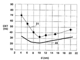
図2には、Ge7Sb76.4Te16.6に対する相変化記録層6または12の厚さd(nm単位)のCET(ns単位)の依存性が、示されている。グラフ21は、結晶化促進層がない場合の関係を表す。また、グラフ22は、記録層6または12が、Si3N4でできていて、かつ2 nmの厚さを有する2つの結晶化促進層にはさまれているときの関係を表す。カーブ21から、CETがd = 10 nmで最小値を有することは、明らかである。さらには、結晶活性化層を適用することによって、CETが記録層6、12の4 nm d =の厚さでさえ35 nsの下にとどまることは明らかである。
FIG. 2 shows the dependency of CET (ns unit) on the thickness d (nm unit) of the phase
図3では、3元図30は、例えば、DVD+RW、DVRまたはBDディスク用の記録層として使用されかつ領域31の化学量論比組成とは離れている「共晶」 GexSbyTez(x+y+z=100)材料を表す、領域32を有する。領域32からの組成を伴う材料は、Geをドープした共晶Sb70Te30とみなすことができ、かつ、成長が支配する結晶化プロセスを有する。これは、マーク消去が、書込まれた非晶質マークと結晶構造環境との間の端から直接成長することによって起こることを意味する。書き込まれた非晶質マークの範囲内での核生成は、成長が完了する前には、生じない。これらの材料のCETは、最初、層の厚さの増加に伴い急速に減少し、その後、図2に示されるように、さらに層の厚さが増加すると再び増加する。最も短い結晶化時間は、約10 nmの厚さで見られる。結晶化時間は、記録用非晶質マーク・サイズの減少に伴い減少するので、これらの共晶(成長型)材料は、1重層DVDおよび2重層DVDの両者とDVR記録システムにおける、高データ転送速度および高密度記録に、最適である。
In Figure 3, a ternary diagram 30, for example, DVD + RW, DVR or stoichiometry away from the composition "eutectic" Ge x Sb y Te in which and
上述の実施例は、本発明を制限するよりむしろ例示として示されていて、当業者は、添付の特許請求の範囲内に限らず、多数の別の実施例を設計することが可能であるという点に、留意されたい。本請求項において、括弧の間に記載されたいかなる参照記号も、本請求項を制限するものとして、解釈されるものではない。「含む(comprising)」という語は、請求項に列挙される内容の範囲以外の要素またはステップの存在を除外するものではない。要素に先立って記載される「1つの(aまたはan)」という語は、これらの要素の複数の存在を、除外するものではない。ある解決手段が、異なる従属クレームにおいて記載されている単なる事実は、これらの解決手段の組合せを有利に用いることができないことを示すものではない。 The embodiments described above are shown by way of illustration rather than limiting the invention, and one skilled in the art will be able to design many other embodiments, not just within the scope of the appended claims. Please note that. In the claims, any reference signs placed between parentheses shall not be construed as limiting the claim. The word “comprising” does not exclude the presence of elements or steps outside the scope of the claims. The word “a” or “an” preceding an element does not exclude the presence of a plurality of these elements. The mere fact that certain solutions are recited in different dependent claims does not indicate that a combination of these solutions cannot be used to advantage.
本発明によれば、記録中に媒体の入射面を介して入射するフォーカスされた放射ビームを使用する、書換え可能な記録用のマルチ・スタック光学データ記憶媒体が、記載されている。この媒体は、第1の相変化型記録層6を含む第1の記録スタックL0の側面に置かれた基板を含む。
In accordance with the present invention, a rewritable multi-stack optical data storage medium for recording is described that uses a focused radiation beam incident through the entrance surface of the medium during recording. This medium includes a substrate placed on the side surface of the first recording stack L 0 including the first phase
第1の記録スタックは、入射面から最も遠い位置に存在する。さらなる相変化型記録層を含む少なくとも1つのさらなる記録スタックLnが、第1の記録スタックよりも入射面の近くに存在する。透明スペーサ層は、記録スタックの間に存在する。さらなる記録層は、4 nm〜12 nmの範囲から選択された厚さを有し、かつ、更なる記録層と接触する、5 nm未満の厚さを有する、少なくとも1枚の透明結晶化促進層を有する、実質的に、原子百分率で式GexSbyTez (ここで、0<x < 15、50< y < 80、10< z < 30およびx + y + z = 100)によって定義される合金である。Lnスタックの記録層の低い結晶化時間と組み合わされた高い光学透過は、媒体を、少なくとも12 m/sの線形記録速度を伴うマルチ・スタック高速記録に適するようにして達成される。 The first recording stack exists at a position farthest from the incident surface. At least one further recording stack L n comprising further phase change recording layers is present closer to the entrance surface than the first recording stack. A transparent spacer layer is present between the recording stacks. The further recording layer has a thickness selected from the range of 4 nm to 12 nm and has a thickness of less than 5 nm in contact with the further recording layer, at least one transparent crystallization promoting layer Substantially defined by the formula Ge x Sb y Te z (where 0 <x <15, 50 <y <80, 10 <z <30 and x + y + z = 100) in atomic percent. Alloy. L n low crystallization time of recording layer combined with high optical transmission of the stack, the medium is accomplished as suitable for multi-stack speed recording with linear recording speed of at least 12 m / s.
1 基板
2, 3 記録スタック
6 第1の相変化型層
11', 13' 透明結晶化促進層
12 相変化型記録層
14 金属反射層
16 入射面
19 レーザ・ビーム
20 マルチ・スタック光学記憶媒体
1 Board
2, 3 record stack
6 First phase change layer
11 ', 13' transparent crystallization promoting layer
12 Phase change recording layer
14 Metal reflective layer
16 Incident surface
19 Laser beam
20 Multi-stack optical storage media
Claims (8)
-その一面に堆積させた基板と、
-前記入射面から最も遠く離れた位置に存在する、第1の相変化型記録層を備える第1の記録スタックL0と、
-前記第1の記録スタックよりも入射面により近く存在するさらなる相変化型記録層を含む、少なくとも1つのさらなる記録スタックLnと、
-前記フォーカスされた放射ビームの焦点深度より大きい厚みを有する、前記記録スタック間の透明なスペーサ層とを、
備えるマルチ・スタック光学データ記憶媒体において
前記さらなる記録層が、実質上、原子百分率式GexSbyTez(0 <x < 15, 50< y < 80, 10< z < 30, x + y + z = 100)によって定義される、4 nm〜12 nmの範囲から選択される厚さを有する合金であり、かつ5 nm未満の厚さを有する、少なくとも1層の透明結晶化促進層が、前記さらなる記録層と接触していることを特徴とする記憶媒体。 A multi-stack optical data storage medium for performing rewritable recording using a focused radiation beam incident through the incident surface of the medium during recording,
-A substrate deposited on one side,
A first recording stack L 0 comprising a first phase change recording layer present at a position furthest away from the incident surface;
-At least one further recording stack L n comprising a further phase change recording layer present closer to the entrance surface than the first recording stack;
A transparent spacer layer between the recording stacks having a thickness greater than the depth of focus of the focused radiation beam;
In the multi-stack optical data storage medium, the further recording layer is substantially composed of an atomic percentage formula Ge x Sb y Te z (0 <x <15, 50 <y <80, 10 <z <30, x + y + z = 100), wherein the transparent crystallization promoting layer is an alloy having a thickness selected from the range of 4 nm to 12 nm and having a thickness of less than 5 nm, A storage medium in contact with a further recording layer.
Applications Claiming Priority (2)
| Application Number | Priority Date | Filing Date | Title |
|---|---|---|---|
| EP02077860 | 2002-07-15 | ||
| PCT/IB2003/002956 WO2004008447A1 (en) | 2002-07-15 | 2003-06-20 | Multi-stack optical data storage medium and use of such medium |
Publications (2)
| Publication Number | Publication Date |
|---|---|
| JP2005533331A true JP2005533331A (en) | 2005-11-04 |
| JP2005533331A5 JP2005533331A5 (en) | 2008-01-10 |
Family
ID=30011200
Family Applications (1)
| Application Number | Title | Priority Date | Filing Date |
|---|---|---|---|
| JP2004520983A Withdrawn JP2005533331A (en) | 2002-07-15 | 2003-06-20 | Multi-stack optical data storage medium and use of the medium |
Country Status (8)
| Country | Link |
|---|---|
| US (1) | US20050177842A1 (en) |
| EP (1) | EP1525580A1 (en) |
| JP (1) | JP2005533331A (en) |
| KR (1) | KR20050026477A (en) |
| CN (1) | CN1669080A (en) |
| AU (1) | AU2003244974A1 (en) |
| TW (1) | TW200403665A (en) |
| WO (1) | WO2004008447A1 (en) |
Cited By (2)
| Publication number | Priority date | Publication date | Assignee | Title |
|---|---|---|---|---|
| JP2008135157A (en) * | 2006-11-01 | 2008-06-12 | Matsushita Electric Ind Co Ltd | Information recording medium, and target and manufacturing method of information recording medium using the same |
| US8017208B2 (en) | 2006-11-01 | 2011-09-13 | Panasonic Corporation | Information recording medium, target and method for manufacturing of information recording medium using the same |
Families Citing this family (1)
| Publication number | Priority date | Publication date | Assignee | Title |
|---|---|---|---|---|
| MXPA06011774A (en) * | 2004-04-15 | 2007-01-16 | Koninkl Philips Electronics Nv | Optical master substrate with mask layer and method to manufacture high-density relief structure. |
Family Cites Families (9)
| Publication number | Priority date | Publication date | Assignee | Title |
|---|---|---|---|---|
| JPH06195747A (en) * | 1992-11-11 | 1994-07-15 | Nec Corp | Optical disc |
| US6143468A (en) * | 1996-10-04 | 2000-11-07 | Mitsubishi Chemical Corporation | Optical information recording medium and optical recording method |
| TW473712B (en) * | 1998-05-12 | 2002-01-21 | Koninkl Philips Electronics Nv | Rewritable double layer optical information medium |
| EP0957477A3 (en) * | 1998-05-15 | 2003-11-05 | Matsushita Electric Industrial Co., Ltd. | Optical information recording medium, recording and reproducing method therefor and optical information recording and reproduction apparatus |
| JP2003532248A (en) * | 2000-04-20 | 2003-10-28 | コーニンクレッカ フィリップス エレクトロニクス エヌ ヴィ | Optical recording medium and use thereof |
| EP1208565B1 (en) * | 2000-07-12 | 2003-11-12 | Koninklijke Philips Electronics N.V. | Optical information medium having separate recording layers |
| TWI233098B (en) * | 2000-08-31 | 2005-05-21 | Matsushita Electric Ind Co Ltd | Data recoding medium, the manufacturing method thereof, and the record reproducing method thereof |
| US20020160306A1 (en) * | 2001-01-31 | 2002-10-31 | Katsunari Hanaoka | Optical information recording medium and method |
| US20030112731A1 (en) * | 2001-09-13 | 2003-06-19 | Shuichi Ohkubo | Phase-change recording medium, recording method and recorder therefor |
-
2003
- 2003-06-20 JP JP2004520983A patent/JP2005533331A/en not_active Withdrawn
- 2003-06-20 KR KR1020057000579A patent/KR20050026477A/en not_active Application Discontinuation
- 2003-06-20 WO PCT/IB2003/002956 patent/WO2004008447A1/en active Application Filing
- 2003-06-20 CN CNA038166399A patent/CN1669080A/en active Pending
- 2003-06-20 AU AU2003244974A patent/AU2003244974A1/en not_active Abandoned
- 2003-06-20 US US10/520,869 patent/US20050177842A1/en not_active Abandoned
- 2003-06-20 EP EP03738448A patent/EP1525580A1/en not_active Withdrawn
- 2003-07-11 TW TW092118990A patent/TW200403665A/en unknown
Cited By (2)
| Publication number | Priority date | Publication date | Assignee | Title |
|---|---|---|---|---|
| JP2008135157A (en) * | 2006-11-01 | 2008-06-12 | Matsushita Electric Ind Co Ltd | Information recording medium, and target and manufacturing method of information recording medium using the same |
| US8017208B2 (en) | 2006-11-01 | 2011-09-13 | Panasonic Corporation | Information recording medium, target and method for manufacturing of information recording medium using the same |
Also Published As
| Publication number | Publication date |
|---|---|
| AU2003244974A1 (en) | 2004-02-02 |
| WO2004008447A1 (en) | 2004-01-22 |
| KR20050026477A (en) | 2005-03-15 |
| EP1525580A1 (en) | 2005-04-27 |
| US20050177842A1 (en) | 2005-08-11 |
| CN1669080A (en) | 2005-09-14 |
| TW200403665A (en) | 2004-03-01 |
Similar Documents
| Publication | Publication Date | Title |
|---|---|---|
| JP4037057B2 (en) | Rewritable optical information medium | |
| US20080253272A1 (en) | Rewritable optical data storage medium and use of such a medium | |
| JP2007128647A (en) | Optical information medium and its use | |
| US6861117B2 (en) | Multi-stack optical data storage medium and use of such medium | |
| US7368223B2 (en) | Multi-stack optical data storage medium and use of such a medium | |
| JP4018340B2 (en) | Rewritable optical information medium | |
| WO2001013370A1 (en) | Rewritable optical information recording medium | |
| EP1393309A1 (en) | Rewritable optical data storage medium and use of such a medium | |
| JP2005533331A (en) | Multi-stack optical data storage medium and use of the medium | |
| JP2005533331A5 (en) | ||
| JP4257211B2 (en) | Rewritable optical storage medium and use of the medium | |
| JP2005537156A (en) | Rewritable optical data storage medium and use of such medium | |
| US7169454B2 (en) | Multi-stack optical data storage medium and use of such medium |
Legal Events
| Date | Code | Title | Description |
|---|---|---|---|
| RD02 | Notification of acceptance of power of attorney |
Free format text: JAPANESE INTERMEDIATE CODE: A7422 Effective date: 20060601 |
|
| A621 | Written request for application examination |
Free format text: JAPANESE INTERMEDIATE CODE: A621 Effective date: 20060619 |
|
| A977 | Report on retrieval |
Free format text: JAPANESE INTERMEDIATE CODE: A971007 Effective date: 20070514 |
|
| A131 | Notification of reasons for refusal |
Free format text: JAPANESE INTERMEDIATE CODE: A131 Effective date: 20070517 |
|
| A601 | Written request for extension of time |
Free format text: JAPANESE INTERMEDIATE CODE: A601 Effective date: 20070815 |
|
| A602 | Written permission of extension of time |
Free format text: JAPANESE INTERMEDIATE CODE: A602 Effective date: 20070822 |
|
| A524 | Written submission of copy of amendment under section 19 (pct) |
Free format text: JAPANESE INTERMEDIATE CODE: A524 Effective date: 20071116 |
|
| A02 | Decision of refusal |
Free format text: JAPANESE INTERMEDIATE CODE: A02 Effective date: 20071225 |
|
| A761 | Written withdrawal of application |
Free format text: JAPANESE INTERMEDIATE CODE: A761 Effective date: 20080711 |