JP2005520218A - High contrast display panel and method for manufacturing high contrast display panel - Google Patents
High contrast display panel and method for manufacturing high contrast display panel Download PDFInfo
- Publication number
- JP2005520218A JP2005520218A JP2004533978A JP2004533978A JP2005520218A JP 2005520218 A JP2005520218 A JP 2005520218A JP 2004533978 A JP2004533978 A JP 2004533978A JP 2004533978 A JP2004533978 A JP 2004533978A JP 2005520218 A JP2005520218 A JP 2005520218A
- Authority
- JP
- Japan
- Prior art keywords
- optical panel
- thickness
- light
- optical
- waveguide
- Prior art date
- Legal status (The legal status is an assumption and is not a legal conclusion. Google has not performed a legal analysis and makes no representation as to the accuracy of the status listed.)
- Withdrawn
Links
- 238000004519 manufacturing process Methods 0.000 title description 2
- 238000000034 method Methods 0.000 title description 2
- 230000003287 optical effect Effects 0.000 claims abstract description 47
- 238000005253 cladding Methods 0.000 claims abstract description 15
- 239000004033 plastic Substances 0.000 claims description 9
- 229920003023 plastic Polymers 0.000 claims description 9
- 229920000642 polymer Polymers 0.000 claims description 5
- 239000011521 glass Substances 0.000 claims description 4
- 238000003384 imaging method Methods 0.000 claims description 3
- 239000000853 adhesive Substances 0.000 description 5
- 230000001070 adhesive effect Effects 0.000 description 5
- 230000005540 biological transmission Effects 0.000 description 3
- 239000007787 solid Substances 0.000 description 3
- 238000004049 embossing Methods 0.000 description 2
- 238000012986 modification Methods 0.000 description 2
- 230000004048 modification Effects 0.000 description 2
- 239000004593 Epoxy Substances 0.000 description 1
- 229920004142 LEXAN™ Polymers 0.000 description 1
- 229920005372 Plexiglas® Polymers 0.000 description 1
- 229920006397 acrylic thermoplastic Polymers 0.000 description 1
- 230000002146 bilateral effect Effects 0.000 description 1
- 239000003086 colorant Substances 0.000 description 1
- 238000010894 electron beam technology Methods 0.000 description 1
- 239000002650 laminated plastic Substances 0.000 description 1
- 239000000463 material Substances 0.000 description 1
- 238000005457 optimization Methods 0.000 description 1
- 230000002093 peripheral effect Effects 0.000 description 1
- 229920003229 poly(methyl methacrylate) Polymers 0.000 description 1
- 239000004926 polymethyl methacrylate Substances 0.000 description 1
- 239000004065 semiconductor Substances 0.000 description 1
- ISXSCDLOGDJUNJ-UHFFFAOYSA-N tert-butyl prop-2-enoate Chemical compound CC(C)(C)OC(=O)C=C ISXSCDLOGDJUNJ-UHFFFAOYSA-N 0.000 description 1
Images

Classifications
-
- G—PHYSICS
- G02—OPTICS
- G02B—OPTICAL ELEMENTS, SYSTEMS OR APPARATUS
- G02B6/00—Light guides; Structural details of arrangements comprising light guides and other optical elements, e.g. couplings
- G02B6/04—Light guides; Structural details of arrangements comprising light guides and other optical elements, e.g. couplings formed by bundles of fibres
- G02B6/06—Light guides; Structural details of arrangements comprising light guides and other optical elements, e.g. couplings formed by bundles of fibres the relative position of the fibres being the same at both ends, e.g. for transporting images
- G02B6/08—Light guides; Structural details of arrangements comprising light guides and other optical elements, e.g. couplings formed by bundles of fibres the relative position of the fibres being the same at both ends, e.g. for transporting images with fibre bundle in form of plate
Abstract
視野コントラストの改善をもたらす光学ディスプレイパネルを開示する。光学パネルは、複数の積層された光導波路であって、各導波路は入口面及び出口面を各導波路の対向する端部に有し、各導波路は少なくとも1つのクラッド層に接触するコアで形成され、少なくとも1つのクラッド層は少なくとも1つの黒色層を有する複数の積層された光導波路と;少なくとも2つの導波路のそれぞれの入口面に接続された少なくとも1つのリディレクターと;を有する。少なくとも1つの黒色層は第1の厚さを有し、コアは第2の厚さを有し、第1の厚さは、好ましくは、第2の厚さの倍である。好ましい実施態様では、第1の厚さは、第2の厚さの少なくとも2倍より大きい。第2の好ましい実施態様では、第1の厚さは、第2の厚さの少なくとも4倍より大きい。An optical display panel that provides improved field contrast is disclosed. The optical panel is a plurality of stacked optical waveguides, each waveguide having an entrance surface and an exit surface at opposite ends of each waveguide, each waveguide being a core in contact with at least one cladding layer And the at least one cladding layer has a plurality of stacked optical waveguides having at least one black layer; and at least one redirector connected to respective entry faces of the at least two waveguides. At least one black layer has a first thickness, the core has a second thickness, and the first thickness is preferably twice the second thickness. In a preferred embodiment, the first thickness is greater than at least twice the second thickness. In a second preferred embodiment, the first thickness is at least four times greater than the second thickness.
Description
本発明は、一般には、平面光学ディスプレイに関するものであり、より詳細には、高コントラストディスプレイパネル及び高コントラストディスプレイパネルの製造方法に関するものである。 The present invention relates generally to planar optical displays, and more particularly to a high contrast display panel and a method for manufacturing a high contrast display panel.
ビデオ(映像)ディスプレイスクリーンは、典型的には、スクリーン(画面)の出口面上に画像を投影するために陰極線管(CRT)を用いる。このタイプの典型的なスクリーンは、幅対高さの比率が4:3で、525本の垂直解像線を有する。集合的に画像を形成する多数の画素(ピクセル)を形成するために、電子ビームをスクリーン上で水平及び垂直の両方向に走査する必要がある。従来の陰極線管は、サイズに実際上の限界があり、所要の電子銃を収容するために比較的奥行きが深い。スクリーン画像サイズを増大するために、一般には種々の形態の画像投影を含む、より大型のスクリーンテレビジョンが利用可能である。しかし、そのようなスクリーンは、特に投影(映写)ディスプレイスクリーンにおいて、限定された視角、限定された解像度、減少された輝度(明度)、及び減少されたコントラストに直面することがある。 A video display screen typically uses a cathode ray tube (CRT) to project an image onto the exit surface of the screen. A typical screen of this type has a width to height ratio of 4: 3 and has 525 vertical resolution lines. In order to form a large number of picture elements (pixels) that collectively form an image, it is necessary to scan the electron beam in both horizontal and vertical directions on the screen. Conventional cathode ray tubes have practical limitations in size and are relatively deep to accommodate the required electron gun. To increase the screen image size, larger screen televisions are generally available, including various forms of image projection. However, such screens may face limited viewing angles, limited resolution, reduced brightness (brightness), and reduced contrast, particularly in projection display screens.
複数の積層された導波路を用いて光学パネルを作製し得ることが知られており、ある光学パネルは、その導波路の透明コア間に少なくとも1つの黒色クラッド層を用いて黒色とされることがある。このクラッド層は、コアを通して導かれる画像光の全反射(全内部反射)を達成するために、導波路コアよりも低い屈折率を有し、これによってコントラストを改善し、即ち、これによってスクリーン上での黒色画像の見かけを改善することができる。 It is known that an optical panel can be made using a plurality of laminated waveguides, and an optical panel is blackened using at least one black cladding layer between the transparent cores of the waveguide. There is. This cladding layer has a lower refractive index than the waveguide core to achieve total reflection of the image light guided through the core (total internal reflection), thereby improving the contrast, i.e. thereby on the screen. The appearance of the black image can be improved.
光学パネルを用いる典型的なテレビジョンの用途においては、光透過(伝達)領域を最大化するために黒色領域は最小化され、これによってスクリーンの輝度を改善する。しかしながら、光学パネルの表面の黒色領域の最小化は、スクリーンコントラストの最適化を許さない。黒色領域の増加のみがスクリーンコントラストの増大を許すという現実のためである。更に、光透過領域の最大化は、同時に、周辺光を反射する領域を増加させ、これによって更にスクリーンコントラスト及び暗さ(ダークネス)を減少させる。 In a typical television application using an optical panel, the black area is minimized to maximize the light transmission (transmission) area, thereby improving screen brightness. However, minimizing the black area on the surface of the optical panel does not allow optimization of screen contrast. This is due to the reality that only an increase in black area allows an increase in screen contrast. Furthermore, maximizing the light transmissive area simultaneously increases the area that reflects ambient light, thereby further reducing screen contrast and darkness.
従って、スクリーン上での黒色領域の外観を増加させ、これによって視野コントラストを改善するディスプレイパネルが必要とされている。 Accordingly, there is a need for a display panel that increases the appearance of black areas on the screen, thereby improving the field contrast.
本発明は、高コントラスト光学パネルに関する。光学パネルは、複数の積層された光導波路であって、各導波路は入口面及び出口面を各導波路の対向する端部に有し、各導波路は少なくとも1つのクラッド層に接触するコアで形成され、前記少なくとも1つのクラッド層は少なくとも1つの黒色層を有する複数の積層された光導波路と;少なくとも2つの導波路のそれぞれの前記入口面に接続された少なくとも1つのリディレクターと;を有する。前記少なくとも1つの黒色層は第1の厚さを有し、前記コアは第2の厚さを有し、前記第1の厚さは、好ましくは、前記第2の厚さよりも大きい。好ましい実施態様では、前記第1の厚さは、前記第2の厚さの少なくとも2倍より大きい。第2の好ましい実施態様では、前記第1の厚さは、前記第2の厚さの少なくとも4倍より大きい。 The present invention relates to a high contrast optical panel. The optical panel is a plurality of stacked optical waveguides, each waveguide having an entrance surface and an exit surface at opposite ends of each waveguide, each waveguide being a core in contact with at least one cladding layer A plurality of stacked optical waveguides, wherein the at least one cladding layer has at least one black layer; and at least one redirector connected to the entrance surface of each of the at least two waveguides; Have. The at least one black layer has a first thickness, the core has a second thickness, and the first thickness is preferably greater than the second thickness. In a preferred embodiment, the first thickness is greater than at least twice the second thickness. In a second preferred embodiment, the first thickness is at least four times greater than the second thickness.
高コントラスト光学ディスプレイパネルは、スクリーン上での黒色領域の外観を増加させ、これによって視野コントラストを改善するディスプレイパネルを提供することによって、従来技術にて経験された問題を解決する。更に、本発明は、光リディレクターからの周辺光の反射を低減する。 High contrast optical display panels solve the problems experienced in the prior art by providing a display panel that increases the appearance of black areas on the screen, thereby improving the field contrast. Furthermore, the present invention reduces the reflection of ambient light from the light redirector.
本発明が明快に理解され、容易に実施されるように、本発明を添付の図面との関連において説明する。 In order that the present invention will be clearly understood and readily implemented, the present invention will be described in connection with the accompanying drawings.
本発明の図面及び説明は、本発明の明快な理解に関連する要素を例示するために単純化され、一方で、明快さを期すために、典型的な光学ディスプレイパネルにおいて見出される他の多くの要素が省略されていることを理解されたい。当業者は、本発明を実施するために他の要素が望ましく且つ/或いは必要とされることを認識するだろう。しかし、そのような要素は斯界にて周知であり、又本発明のより良い理解を促進することはないので、そのような要素の議論は本明細書では提供されない。 The drawings and descriptions of the present invention have been simplified to illustrate elements relevant to a clear understanding of the present invention, while many others found in a typical optical display panel for clarity. It should be understood that the elements are omitted. Those skilled in the art will recognize that other elements are desirable and / or required to practice the present invention. However, discussion of such elements is not provided herein because such elements are well known in the art and do not facilitate a better understanding of the present invention.
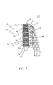
図1は、ディスプレイパネル10を示す概略断面図である。ディスプレイパネル10は、複数の積層された導波路16aと、光発生器21と、を有する。各導波路16aは、その間に黒色層、例えば黒色クラッド層を、ボディー(本体)18の一端部において複数の積層された導波路16aによって形成される出口面16を、ボディー18の第2の端部において入口面12を有する。入口面12は、好ましくは、その上に、リディレクター(再指向体)19、例えば3M(登録商標)・コーポレイション[ミネアポリス、ミネソタ州]によって製造されるTRAF、又は同様の構造を有する。
FIG. 1 is a schematic cross-sectional view showing a
ボディー18は、好ましくは、中実(固体)であり、光14を入口面12の表面に沿って受容する。好ましい実施態様では、入口面は、その上に、入口面12に入射する光を導波路16a内へと再指向させるリディレクター19、例えばTRAF、TRAF様のもの、又は同様の構造を有する。光14は、入口面12に入った後にボディー18を通過させられ、そしてボディー18を通して出口面16へと実質的に全反射される。本発明の好ましい実施態様において、ボディー18は、複数の積層された導波路16aの長さ、高さ、及び幅に形成される。
The
複数の積層された導波路16aは、パネル10のボディー18を形成し、この積層体16aの一端部において入口面12を、又第2の端部において出口面16を形成する。導波路16aは、限定されるものではないが、例えばプラスチック類、又はガラスのような、それを通して電磁波を通過させるのに適することが斯界にて知られている任意の材料で形成することができる。本発明の好ましい実施態様は、個別のガラス、プラスチック又はポリマーのシートを用いて実施され、これらは、典型的には、厚さが0.001〜0.020インチ(2.54〜50.8μm)であり、又扱いやすい長さ及び幅であってよい。勿論、ディスプレイの全体の寸法に応じて、各個々のガラス、プラスチック又はポリマーのシートのために他の厚さを採用することができる。使用されるポリマーは、適当なプラスチックラミネート、例えばジェネラル・エレクトリック・カンパニー(登録商標)から市販されているLexan(レクサン)(登録商標)、又はプレキシガラス(Plexiglass)のようなポリマー類若しくはアクリル類などであってよい。
The plurality of laminated
導波路16aは、出口面16の幅全体に延在するシート又はリボンの形態であり、そしてそれらの上端部において出口面16の高さを集合的に形成するように積み重ねられる。導波路群16aは、それらの長手方向光透過軸に沿って配置される。導波路16aの数は、出口面16の対応する垂直解像度を提供するように選択することができる。例えば、525個の導波路16aを、出口面16内に525本の垂直解像線を生成するために積み重ねることができる。各垂直解像線のために、幾つかの導波路を任意に用いることができる。複数(多重)の導波路が採用される実施態様は、入射する画像光に対するスクリーンの整列許容範囲の臨界性を減少させる。導波路16aは出口面16の幅全体に延在するので、水平解像度は、画像光14の水平方向変調によって制御することができる。
The
複数の導波路のそれぞれは、導波路を通して画像光14を導くための中央コア26を有し、各コア26はクラッド層28間に配置される。本発明の好ましい実施態様では、クラッド層28は、出口面16の全幅に沿って入口面12から出口面16へと完全に延びる。黒色層30は、出口面16において周辺光32を吸収するように、隣接するクラッド層28の中若しくは間に配置することができ、多層(マルチレイヤー)クラッド28を形成することができる。本明細書で使用される黒色という用語は、純粋な黒色だけではなく、加えて、本発明において使用するのに適した機能的に匹敵する暗色、例えば紺(ダークブルー)をも包含する。黒色層30は、出口面の可視領域内でのみ必要であるが、本発明の好ましい実施態様では、黒色層30は、入口面12から出口面16へと出口面16の全幅に沿って完全に延びる。更に、クラッド層28は、暗い勾配屈折率層で形成することができる。
Each of the plurality of waveguides has a central core 26 for guiding the
本発明の好ましい実施態様では、クラッド層であるか若しくはクラッド層間にあってよい黒色層は、各導波路/クラッド/黒色層の層の80%を構成する。例えば、クリア(透明)な導波路コアは、出口面16における黒色層の厚さの1/4であろう。従って、黒色層の厚さは、クリア層の、即ち、コアの厚さの、少なくとも、例えば、倍より大きいか若しくは等しい。好ましい実施態様において、黒色層は、入口面12へと延在するが、リディレクター19の縁(エッジ)までは延在しない。別法では、黒色層は、リディレクター19の縁まで延在していてよく、従って光発生器21からの入力光の経路に近接する。
In a preferred embodiment of the invention, the black layer, which may be a clad layer or be between clad layers, constitutes 80% of each waveguide / clad / black layer. For example, a clear (transparent) waveguide core would be 1/4 of the thickness of the black layer at the
更に、リディレクター19、例えばTRAF若しくはTRAF様のプリズム構造の使用は、中央コアに対する、各層の厚さの約20%だけの提供と関連して、リディレクター19の周辺反射領域を減少させる。それによって、周辺光が使用できる有用な領域は、リディレクター19の20%だけに限定される。従って、反射された周辺光は、入口面において更に減少され、それによって出口面16におけるスクリーンの暗さ及びコントラストを更に改善する。
Furthermore, the use of a
各中央コア26は、第1の屈折率を有する。上述して議論したように黒色であってよいクラッド層28は、入口面12から出口面16へと画像光14が進む際に画像光14の全反射を確実とするために、中央コア26のそれよりも低い第2の屈折率を有する。黒色層30は、クラッド層から独立である場合、任意の屈折率を有していてよいが、やはり中央コア26の厚さと等しいか若しくは実質的にそれより大きいことが好ましい。
Each central core 26 has a first refractive index. As discussed above, the
入口面12及び出口面16は、複数の導波路16aで形成され、各導波路16aの一端部はその導波路のための入口を形成し、各導波路16aの反対側の端部はその導波路16aのための出口を形成する。各導波路16aは、水平方向に延在し、複数の積層された導波路16aは垂直方向に延びる。光14は、限定されるものではないが、例えばビデオ画像14aの形態にて出口面上に表示することができる。従って、好ましい実施態様では、複数の導波路16aは、水平線と略平行に積み重ねられ、斯くして出口面16及び入口面12を、水平線に対し同一面内で、水平線から略等距離に配置する。
The
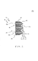
入口面12は、複数の積層された光導波路16aによって形成される。入口面12は、ボディー18の一端部に位置し、光発生器21からの光14を受容する。入口面は、平坦若しくは鋸歯状であってよい。黒色層は、出口面へと延在していてよいが、図1に示すように、リディレクター19までは延在しないか、又は、図2に示すように、リディレクター19を通して延在していてよい。好ましい実施態様においては、入口面12は、その上に、例えば接着剤、エポキシ又はエンボス加工によってそれに固定された、少なくとも1つのリディレクター19を有する。出口面16は、ボディー18の前面として規定され、そして出口面は、図1及び2に示すように平坦であるか、又は図3に示すように例えば中央コアの出口点に近接し又これを含む平坦領域だけを有するような鋸歯状であってよい。出口面16は、付加的に、例えばエンボス加工によって包含しているか、又は付着などによってその上に有する、拡散器(ディフューザー)を、例えば、観察者に対し改善された画像14aを提供するように有していてよい。尚、パネル10は、出口面16の頂部から底部までの高さを有し、又出口面16の左側から右側への幅を有する。幅及び高さは、例えば、典型的なテレビジョンの用途での使用のために、4:3又は16:9の幅対高さのアスペクト比を生成するように選択することができる。
The
光発生器21は光14を発生し、又光を入口面16へと通過させる。光14は、好ましくは、急な入射角にてリディレクター19を射る。光発生器21は、例えばオーバーヘッドプロジェクターのような白色光投影器(プロジェクター)であってよく、或いは例えばビデオ又はムービープロジェクターのような、光源、及び/又は光変調器(ライトモジュレーター)、及び/又は結像光学系を有していてよい。光14は、最初に、例えば、光源によって発生することができる。光源は、例えば、明るい白熱電球、レーザ、アーク灯、LED、RF励起ガス放電灯、任意の固体(半導体)光源、又は任意の燐光性(ホスホレセント)、発光性(ルミネセント)、若しくは白熱性の光源であってよい。光源からの光14は、次いで斯界において画素(ピクセル)として知られている個々の描画要素を規定するように、変調器によって変調することができる。或いは、光は、例えばオン/オフスイッチのような、単純な照明されたアイテムを規定することができる。結像光学系は、光折り返しミラー類又はレンズ類を有していてよい。光学系は、出口面16へと画像を正確に供給するために、所望により光14を圧縮若しくは拡大及び集束(フォーカシング)するように、出口面16と光変調器との間に光学的に整列することができる。光14は、リディレクター19から入口面12に入った後、パネルボディー18を通して出口面16へと進む。
The
好ましい実施態様では、好ましくは約1/2インチ×40インチ(1.27cm×101.6cm)、厚さが約20/1000インチ(0.0508cm)である、クリアなプラスチックのストリップ(細長い一片)が、各プラスチックストリップ間の両側性の黒色接着剤と共に、又は各ストリップ間の暗色の勾配(ダークグラジエント)と共に積み重ねられる。暗色、又は黒色の層は、好ましくは、各積み重ね(レイヤリング)においてプラスチックストリップの厚さの少なくとも約4倍である。ストリップの積層体は、次いで、気泡を除去し、又接着を増進するように高圧力下でプレスされる。接着剤は、黒色以外の、例えば紺(ダークブルー)のような薄い暗色(シェード)であってよく、又好ましくはテープ形態のように転がり出る、プラスチック/接着剤/プラスチック/接着剤の形式のものであってよい。完成した積層体に適用される圧力は、好ましくは1,000ポンド(≒453.6kg)超である。 In a preferred embodiment, a clear plastic strip, preferably about 1/2 "x 40" (1.27 cm x 101.6 cm) and about 20/1000 "(0.0508 cm) thick. Are stacked with a bilateral black adhesive between each plastic strip, or with a dark gradient between each strip. The dark or black layer is preferably at least about 4 times the thickness of the plastic strip in each stack. The laminate of strips is then pressed under high pressure to remove bubbles and promote adhesion. The adhesive can be a light shade other than black, for example dark blue, and preferably rolls like a tape form in the form of plastic / adhesive / plastic / adhesive. It may be a thing. The pressure applied to the finished laminate is preferably greater than 1,000 pounds (≈453.6 kg).
当業者は、本発明の多くの改変及び変更を実施し得ると認識するであろう。上述の説明及び添付の特許請求の範囲は、そのような改変及び変更の全てを包含することを意図する。 Those skilled in the art will recognize that many modifications and variations of the present invention may be implemented. The above description and the appended claims are intended to cover all such modifications and changes.
Claims (20)
少なくとも2つの導波路のそれぞれの前記入口面に接続された少なくとも1つのリディレクターと、
を有し、
前記少なくとも1つの黒色層は第1の厚さを有し、前記コアは第2の厚さを有し、前記第1の厚さは、前記第2の厚さの少なくとも倍であることを特徴とする光学パネル。 A plurality of stacked optical waveguides, each waveguide having an entrance surface and an exit surface at opposite ends of each waveguide, each waveguide formed of a core in contact with at least one cladding layer; The at least one cladding layer includes a plurality of stacked optical waveguides having at least one black layer;
At least one redirector connected to the entrance face of each of at least two waveguides;
Have
The at least one black layer has a first thickness, the core has a second thickness, and the first thickness is at least twice the second thickness. An optical panel.
Applications Claiming Priority (2)
| Application Number | Priority Date | Filing Date | Title |
|---|---|---|---|
| US09/861,459 US6571044B2 (en) | 2001-05-18 | 2001-05-18 | High contrast display panel and a method of making a high contrast display panel |
| PCT/US2002/015751 WO2004023176A1 (en) | 2001-05-18 | 2002-05-17 | A high contrast display panel |
Publications (2)
| Publication Number | Publication Date |
|---|---|
| JP2005520218A true JP2005520218A (en) | 2005-07-07 |
| JP2005520218A5 JP2005520218A5 (en) | 2006-01-05 |
Family
ID=25335853
Family Applications (1)
| Application Number | Title | Priority Date | Filing Date |
|---|---|---|---|
| JP2004533978A Withdrawn JP2005520218A (en) | 2001-05-18 | 2002-05-17 | High contrast display panel and method for manufacturing high contrast display panel |
Country Status (5)
| Country | Link |
|---|---|
| US (1) | US6571044B2 (en) |
| EP (1) | EP1428050A4 (en) |
| JP (1) | JP2005520218A (en) |
| CA (1) | CA2454550A1 (en) |
| WO (1) | WO2004023176A1 (en) |
Families Citing this family (7)
| Publication number | Priority date | Publication date | Assignee | Title |
|---|---|---|---|---|
| US7187831B2 (en) * | 2004-04-26 | 2007-03-06 | Brookhaven Science Associates | Optical panel system including stackable waveguides |
| US20080112677A1 (en) * | 2006-06-21 | 2008-05-15 | Ronald Smith | Optical Display System and Method |
| US7412131B2 (en) * | 2007-01-02 | 2008-08-12 | General Electric Company | Multilayer optic device and system and method for making same |
| US20080285125A1 (en) * | 2007-05-18 | 2008-11-20 | Fujifilm Manufacturing U.S.A. Inc. | Optical panel for front projection under ambient lighting conditions |
| US20080291169A1 (en) * | 2007-05-21 | 2008-11-27 | Brenner David S | Multimodal Adaptive User Interface for a Portable Electronic Device |
| US7496263B2 (en) * | 2007-06-07 | 2009-02-24 | Fujifilm Manfacturing U.S.A. Inc. | Thermosetting optical waveguide coating |
| US20080305255A1 (en) * | 2007-06-07 | 2008-12-11 | Fujifilm Manufacturing U.S.A. Inc. | Optical waveguide coating |
Family Cites Families (33)
| Publication number | Priority date | Publication date | Assignee | Title |
|---|---|---|---|---|
| US3253500A (en) | 1964-05-11 | 1966-05-31 | American Optical Corp | Doubly clad light-conducting fibers with the outer cladding being partially light absorbing |
| US3874783A (en) | 1972-08-02 | 1975-04-01 | American Optical Corp | Numerical aperture expansion in fiber optic devices |
| US4116739A (en) | 1976-11-26 | 1978-09-26 | New York Institute Of Technology | Method of forming an optical fiber device |
| US4344668A (en) | 1980-03-17 | 1982-08-17 | Hughes Aircraft Company | Fiber optic light traps for electro-optical display devices |
| US4418986A (en) | 1981-04-07 | 1983-12-06 | Mitsubishi Rayon Co., Ltd. | Rear projection screen |
| US4469402A (en) | 1981-06-15 | 1984-09-04 | Mitsubishi Rayon Co., Ltd. | Rear projection screen |
| US4586781A (en) | 1982-07-30 | 1986-05-06 | Hughes Aircraft Company | Diffraction optics diffusing screen |
| JPS61208041A (en) | 1985-03-11 | 1986-09-16 | Mitsubishi Rayon Co Ltd | Back face projection screen |
| US5274406A (en) | 1987-12-29 | 1993-12-28 | Asahi Kogaku Kogyo Kabushiki Kaisha | Image projecting device |
| FR2626700B1 (en) | 1988-02-03 | 1992-12-04 | Castel Francois Du | VERY LARGE DIMENSIONS DISPLAY |
| US5422691A (en) | 1991-03-15 | 1995-06-06 | Seiko Epson Corporation | Projection type displaying apparatus and illumination system |
| US5481385A (en) | 1993-07-01 | 1996-01-02 | Alliedsignal Inc. | Direct view display device with array of tapered waveguide on viewer side |
| US5764845A (en) | 1993-08-03 | 1998-06-09 | Fujitsu Limited | Light guide device, light source device, and liquid crystal display device |
| GB2282671B (en) | 1993-10-08 | 1997-12-10 | Durand Ltd | Diffusing and depixelating means |
| US5381502A (en) | 1993-09-29 | 1995-01-10 | Associated Universities, Inc. | Flat or curved thin optical display panel |
| US5455882A (en) | 1993-09-29 | 1995-10-03 | Associated Universities, Inc. | Interactive optical panel |
| US5521725A (en) | 1993-11-05 | 1996-05-28 | Alliedsignal Inc. | Illumination system employing an array of microprisms |
| JPH08338916A (en) * | 1995-06-12 | 1996-12-24 | Hamamatsu Photonics Kk | Fiber optical plate |
| JP3541576B2 (en) | 1995-10-25 | 2004-07-14 | ミノルタ株式会社 | Imaging optics |
| US5625736A (en) | 1996-01-11 | 1997-04-29 | Associated Universities, Inc. | Black optic display |
| US5668907A (en) | 1996-01-11 | 1997-09-16 | Associated Universities, Inc. | Thin optical display panel |
| JPH09265264A (en) | 1996-03-27 | 1997-10-07 | Casio Comput Co Ltd | Display device |
| US5914760A (en) | 1996-06-21 | 1999-06-22 | Casio Computer Co., Ltd. | Surface light source device and liquid crystal display device using the same |
| US5940565A (en) * | 1996-07-24 | 1999-08-17 | Hamamatsu Photonics K.K. | Fiber optic device, light receiving member, and pattern acquisition apparatus |
| US6012816A (en) | 1996-10-08 | 2000-01-11 | Beiser; Leo | Optical projection apparatus and method |
| JPH10160948A (en) * | 1996-12-04 | 1998-06-19 | Hamamatsu Photonics Kk | Fiber optic plate |
| JP2858656B2 (en) | 1997-02-14 | 1999-02-17 | 日立電線株式会社 | Optical wavelength multiplexer / demultiplexer |
| US6487350B1 (en) * | 1998-07-16 | 2002-11-26 | Brookhaven Science Associates | Multi-clad black display panel |
| US6222971B1 (en) * | 1998-07-17 | 2001-04-24 | David Slobodin | Small inlet optical panel and a method of making a small inlet optical panel |
| US6002826A (en) | 1998-08-28 | 1999-12-14 | Brookhaven Science Associates | Thin display optical projector |
| US6301417B1 (en) | 1998-08-31 | 2001-10-09 | Brookhaven Science Associates | Ultrathin optical panel and a method of making an ultrathin optical panel |
| US6259855B1 (en) * | 1998-12-02 | 2001-07-10 | 3M Innovative Properties Co. | Illumination device and method for making the same |
| US6317545B1 (en) * | 1999-09-01 | 2001-11-13 | James T. Veligdan | Stepped inlet optical panel |
-
2001
- 2001-05-18 US US09/861,459 patent/US6571044B2/en not_active Expired - Fee Related
-
2002
- 2002-05-17 EP EP02807659A patent/EP1428050A4/en not_active Withdrawn
- 2002-05-17 CA CA002454550A patent/CA2454550A1/en not_active Abandoned
- 2002-05-17 WO PCT/US2002/015751 patent/WO2004023176A1/en not_active Application Discontinuation
- 2002-05-17 JP JP2004533978A patent/JP2005520218A/en not_active Withdrawn
Also Published As
| Publication number | Publication date |
|---|---|
| EP1428050A4 (en) | 2005-06-29 |
| US20020172480A1 (en) | 2002-11-21 |
| CA2454550A1 (en) | 2002-11-18 |
| WO2004023176A1 (en) | 2004-03-18 |
| US6571044B2 (en) | 2003-05-27 |
| EP1428050A1 (en) | 2004-06-16 |
Similar Documents
| Publication | Publication Date | Title |
|---|---|---|
| JP4205945B2 (en) | High contrast front projection display panel and method of manufacturing high contrast front projection display panel | |
| US6685792B2 (en) | Method of making a small inlet optical panel | |
| US6751019B2 (en) | Ultrathin mesh optical panel and a method of making an ultrathin mesh optical panel | |
| US6782178B2 (en) | Planar optical waveguides for optical panel having gradient refractive index core | |
| KR20010074869A (en) | Ultrathin optical panel and a method of making an ultrathin optical panel | |
| US20020048438A1 (en) | Transparent seam display panel and a method of making a transparent seam display panel | |
| JP2002520668A (en) | Multi-clad black display panel | |
| US7324278B2 (en) | Black matrix light guide screen display | |
| US6571044B2 (en) | High contrast display panel and a method of making a high contrast display panel | |
| US7421180B2 (en) | Light guide apparatus for use in rear projection display environments | |
| US7477814B2 (en) | Method of making a louver device for a light guide screen | |
| US7256951B2 (en) | Light guide display with protective layer | |
| US7431488B2 (en) | Light guide display with antireflection film | |
| US20060176451A1 (en) | Fiber optic rear projection display | |
| US20060239626A1 (en) | Lossy clad light guide screen |
Legal Events
| Date | Code | Title | Description |
|---|---|---|---|
| A521 | Request for written amendment filed |
Free format text: JAPANESE INTERMEDIATE CODE: A523 Effective date: 20050511 |
|
| A621 | Written request for application examination |
Free format text: JAPANESE INTERMEDIATE CODE: A621 Effective date: 20050511 |
|
| A761 | Written withdrawal of application |
Free format text: JAPANESE INTERMEDIATE CODE: A761 Effective date: 20061211 |