JP2005510871A - Manufacturing method of semiconductor device - Google Patents
Manufacturing method of semiconductor device Download PDFInfo
- Publication number
- JP2005510871A JP2005510871A JP2003548292A JP2003548292A JP2005510871A JP 2005510871 A JP2005510871 A JP 2005510871A JP 2003548292 A JP2003548292 A JP 2003548292A JP 2003548292 A JP2003548292 A JP 2003548292A JP 2005510871 A JP2005510871 A JP 2005510871A
- Authority
- JP
- Japan
- Prior art keywords
- surface layer
- amorphous
- semiconductor
- dopant atoms
- radiation
- Prior art date
- Legal status (The legal status is an assumption and is not a legal conclusion. Google has not performed a legal analysis and makes no representation as to the accuracy of the status listed.)
- Pending
Links
- 239000004065 semiconductor Substances 0.000 title claims abstract description 81
- 238000004519 manufacturing process Methods 0.000 title claims abstract description 12
- 239000002344 surface layer Substances 0.000 claims abstract description 57
- 238000000034 method Methods 0.000 claims abstract description 41
- 230000005855 radiation Effects 0.000 claims abstract description 23
- 239000013078 crystal Substances 0.000 claims abstract description 19
- 238000005280 amorphization Methods 0.000 claims abstract description 10
- 230000004907 flux Effects 0.000 claims abstract description 9
- 239000002019 doping agent Substances 0.000 claims description 39
- 239000000463 material Substances 0.000 claims description 25
- 239000010410 layer Substances 0.000 claims description 15
- 238000004151 rapid thermal annealing Methods 0.000 claims description 11
- 238000010521 absorption reaction Methods 0.000 claims description 10
- 238000002844 melting Methods 0.000 claims description 7
- 230000008018 melting Effects 0.000 claims description 7
- 238000005468 ion implantation Methods 0.000 claims description 6
- 238000001816 cooling Methods 0.000 claims description 4
- 238000005224 laser annealing Methods 0.000 claims description 3
- 239000000155 melt Substances 0.000 claims 1
- 239000007787 solid Substances 0.000 claims 1
- 230000001678 irradiating effect Effects 0.000 abstract 1
- 238000002513 implantation Methods 0.000 description 19
- 238000009792 diffusion process Methods 0.000 description 14
- 230000004913 activation Effects 0.000 description 8
- 238000001953 recrystallisation Methods 0.000 description 8
- 150000002500 ions Chemical class 0.000 description 7
- 230000008569 process Effects 0.000 description 6
- 229910052710 silicon Inorganic materials 0.000 description 6
- 230000000694 effects Effects 0.000 description 5
- 229910052732 germanium Inorganic materials 0.000 description 5
- 238000010438 heat treatment Methods 0.000 description 5
- ATJFFYVFTNAWJD-UHFFFAOYSA-N Tin Chemical compound [Sn] ATJFFYVFTNAWJD-UHFFFAOYSA-N 0.000 description 4
- 239000007791 liquid phase Substances 0.000 description 4
- 239000007790 solid phase Substances 0.000 description 4
- 238000000348 solid-phase epitaxy Methods 0.000 description 4
- 125000006850 spacer group Chemical group 0.000 description 4
- XUIMIQQOPSSXEZ-UHFFFAOYSA-N Silicon Chemical compound [Si] XUIMIQQOPSSXEZ-UHFFFAOYSA-N 0.000 description 3
- 238000000137 annealing Methods 0.000 description 3
- 238000004090 dissolution Methods 0.000 description 3
- 238000004943 liquid phase epitaxy Methods 0.000 description 3
- 239000010703 silicon Substances 0.000 description 3
- XKRFYHLGVUSROY-UHFFFAOYSA-N Argon Chemical compound [Ar] XKRFYHLGVUSROY-UHFFFAOYSA-N 0.000 description 2
- BOTDANWDWHJENH-UHFFFAOYSA-N Tetraethyl orthosilicate Chemical compound CCO[Si](OCC)(OCC)OCC BOTDANWDWHJENH-UHFFFAOYSA-N 0.000 description 2
- 229910021417 amorphous silicon Inorganic materials 0.000 description 2
- 230000009286 beneficial effect Effects 0.000 description 2
- 229910052796 boron Inorganic materials 0.000 description 2
- 150000001875 compounds Chemical class 0.000 description 2
- 229910021419 crystalline silicon Inorganic materials 0.000 description 2
- 230000007547 defect Effects 0.000 description 2
- 238000010586 diagram Methods 0.000 description 2
- GNPVGFCGXDBREM-UHFFFAOYSA-N germanium atom Chemical compound [Ge] GNPVGFCGXDBREM-UHFFFAOYSA-N 0.000 description 2
- 239000011521 glass Substances 0.000 description 2
- 229910052698 phosphorus Inorganic materials 0.000 description 2
- 229910021420 polycrystalline silicon Inorganic materials 0.000 description 2
- PXGOKWXKJXAPGV-UHFFFAOYSA-N Fluorine Chemical compound FF PXGOKWXKJXAPGV-UHFFFAOYSA-N 0.000 description 1
- 229910052581 Si3N4 Inorganic materials 0.000 description 1
- 230000002745 absorbent Effects 0.000 description 1
- 239000002250 absorbent Substances 0.000 description 1
- 230000003213 activating effect Effects 0.000 description 1
- 229910052787 antimony Inorganic materials 0.000 description 1
- 229910052786 argon Inorganic materials 0.000 description 1
- 229910052785 arsenic Inorganic materials 0.000 description 1
- 230000004888 barrier function Effects 0.000 description 1
- 230000008901 benefit Effects 0.000 description 1
- 230000015572 biosynthetic process Effects 0.000 description 1
- 239000000919 ceramic Substances 0.000 description 1
- 230000005465 channeling Effects 0.000 description 1
- 238000003486 chemical etching Methods 0.000 description 1
- 230000009849 deactivation Effects 0.000 description 1
- 238000009826 distribution Methods 0.000 description 1
- 229910052731 fluorine Inorganic materials 0.000 description 1
- 239000011737 fluorine Substances 0.000 description 1
- 230000006870 function Effects 0.000 description 1
- 239000012212 insulator Substances 0.000 description 1
- 230000005596 ionic collisions Effects 0.000 description 1
- 238000002955 isolation Methods 0.000 description 1
- 239000007788 liquid Substances 0.000 description 1
- 239000002184 metal Substances 0.000 description 1
- 230000003287 optical effect Effects 0.000 description 1
- 238000001020 plasma etching Methods 0.000 description 1
- 229920005591 polysilicon Polymers 0.000 description 1
- 230000009467 reduction Effects 0.000 description 1
- HQVNEWCFYHHQES-UHFFFAOYSA-N silicon nitride Chemical compound N12[Si]34N5[Si]62N3[Si]51N64 HQVNEWCFYHHQES-UHFFFAOYSA-N 0.000 description 1
- 239000000758 substrate Substances 0.000 description 1
- 238000004781 supercooling Methods 0.000 description 1
- 230000003746 surface roughness Effects 0.000 description 1
- 238000012876 topography Methods 0.000 description 1
Images


Classifications
-
- H—ELECTRICITY
- H01—ELECTRIC ELEMENTS
- H01L—SEMICONDUCTOR DEVICES NOT COVERED BY CLASS H10
- H01L21/00—Processes or apparatus adapted for the manufacture or treatment of semiconductor or solid state devices or of parts thereof
- H01L21/02—Manufacture or treatment of semiconductor devices or of parts thereof
- H01L21/04—Manufacture or treatment of semiconductor devices or of parts thereof the devices having at least one potential-jump barrier or surface barrier, e.g. PN junction, depletion layer or carrier concentration layer
- H01L21/18—Manufacture or treatment of semiconductor devices or of parts thereof the devices having at least one potential-jump barrier or surface barrier, e.g. PN junction, depletion layer or carrier concentration layer the devices having semiconductor bodies comprising elements of Group IV of the Periodic System or AIIIBV compounds with or without impurities, e.g. doping materials
- H01L21/26—Bombardment with radiation
- H01L21/263—Bombardment with radiation with high-energy radiation
- H01L21/265—Bombardment with radiation with high-energy radiation producing ion implantation
- H01L21/26506—Bombardment with radiation with high-energy radiation producing ion implantation in group IV semiconductors
- H01L21/26513—Bombardment with radiation with high-energy radiation producing ion implantation in group IV semiconductors of electrically active species
-
- H—ELECTRICITY
- H01—ELECTRIC ELEMENTS
- H01L—SEMICONDUCTOR DEVICES NOT COVERED BY CLASS H10
- H01L21/00—Processes or apparatus adapted for the manufacture or treatment of semiconductor or solid state devices or of parts thereof
- H01L21/02—Manufacture or treatment of semiconductor devices or of parts thereof
- H01L21/04—Manufacture or treatment of semiconductor devices or of parts thereof the devices having at least one potential-jump barrier or surface barrier, e.g. PN junction, depletion layer or carrier concentration layer
- H01L21/18—Manufacture or treatment of semiconductor devices or of parts thereof the devices having at least one potential-jump barrier or surface barrier, e.g. PN junction, depletion layer or carrier concentration layer the devices having semiconductor bodies comprising elements of Group IV of the Periodic System or AIIIBV compounds with or without impurities, e.g. doping materials
- H01L21/26—Bombardment with radiation
- H01L21/263—Bombardment with radiation with high-energy radiation
- H01L21/265—Bombardment with radiation with high-energy radiation producing ion implantation
- H01L21/26506—Bombardment with radiation with high-energy radiation producing ion implantation in group IV semiconductors
- H01L21/26513—Bombardment with radiation with high-energy radiation producing ion implantation in group IV semiconductors of electrically active species
- H01L21/2652—Through-implantation
-
- H—ELECTRICITY
- H01—ELECTRIC ELEMENTS
- H01L—SEMICONDUCTOR DEVICES NOT COVERED BY CLASS H10
- H01L21/00—Processes or apparatus adapted for the manufacture or treatment of semiconductor or solid state devices or of parts thereof
- H01L21/02—Manufacture or treatment of semiconductor devices or of parts thereof
- H01L21/04—Manufacture or treatment of semiconductor devices or of parts thereof the devices having at least one potential-jump barrier or surface barrier, e.g. PN junction, depletion layer or carrier concentration layer
- H01L21/18—Manufacture or treatment of semiconductor devices or of parts thereof the devices having at least one potential-jump barrier or surface barrier, e.g. PN junction, depletion layer or carrier concentration layer the devices having semiconductor bodies comprising elements of Group IV of the Periodic System or AIIIBV compounds with or without impurities, e.g. doping materials
- H01L21/26—Bombardment with radiation
- H01L21/263—Bombardment with radiation with high-energy radiation
- H01L21/268—Bombardment with radiation with high-energy radiation using electromagnetic radiation, e.g. laser radiation
-
- H—ELECTRICITY
- H01—ELECTRIC ELEMENTS
- H01L—SEMICONDUCTOR DEVICES NOT COVERED BY CLASS H10
- H01L21/00—Processes or apparatus adapted for the manufacture or treatment of semiconductor or solid state devices or of parts thereof
- H01L21/02—Manufacture or treatment of semiconductor devices or of parts thereof
- H01L21/04—Manufacture or treatment of semiconductor devices or of parts thereof the devices having at least one potential-jump barrier or surface barrier, e.g. PN junction, depletion layer or carrier concentration layer
- H01L21/18—Manufacture or treatment of semiconductor devices or of parts thereof the devices having at least one potential-jump barrier or surface barrier, e.g. PN junction, depletion layer or carrier concentration layer the devices having semiconductor bodies comprising elements of Group IV of the Periodic System or AIIIBV compounds with or without impurities, e.g. doping materials
- H01L21/30—Treatment of semiconductor bodies using processes or apparatus not provided for in groups H01L21/20 - H01L21/26
- H01L21/324—Thermal treatment for modifying the properties of semiconductor bodies, e.g. annealing, sintering
-
- H—ELECTRICITY
- H01—ELECTRIC ELEMENTS
- H01L—SEMICONDUCTOR DEVICES NOT COVERED BY CLASS H10
- H01L29/00—Semiconductor devices adapted for rectifying, amplifying, oscillating or switching, or capacitors or resistors with at least one potential-jump barrier or surface barrier, e.g. PN junction depletion layer or carrier concentration layer; Details of semiconductor bodies or of electrodes thereof ; Multistep manufacturing processes therefor
- H01L29/66—Types of semiconductor device ; Multistep manufacturing processes therefor
- H01L29/66007—Multistep manufacturing processes
- H01L29/66075—Multistep manufacturing processes of devices having semiconductor bodies comprising group 14 or group 13/15 materials
- H01L29/66227—Multistep manufacturing processes of devices having semiconductor bodies comprising group 14 or group 13/15 materials the devices being controllable only by the electric current supplied or the electric potential applied, to an electrode which does not carry the current to be rectified, amplified or switched, e.g. three-terminal devices
- H01L29/66409—Unipolar field-effect transistors
- H01L29/66477—Unipolar field-effect transistors with an insulated gate, i.e. MISFET
- H01L29/66568—Lateral single gate silicon transistors
- H01L29/66575—Lateral single gate silicon transistors where the source and drain or source and drain extensions are self-aligned to the sides of the gate
Abstract
半導体ボディ(2)を有する半導体装置(1)の製造方法において、ドープ領域(3)が半導体ボディ(2)に形成される。半導体ボディ(2)は、結晶表面領域(4)を有し、この結晶表面領域(4)を、少なくとも部分的に非晶質化し、非晶質表面層(5)を形成する。非晶質化は、表面(6)に、結晶表面領域(4)により吸収される放射パルス(7)を照射することにより達成される。放射パルス(7)は、放射が結晶表面領域(4)に吸収されるように選択された波長を有し、放射パルス(7)のエネルギー束は、結晶表面層(5)を溶解させるように選択される。この方法は、非常に浅い接合の製作に有用である。 In the method for manufacturing a semiconductor device (1) having a semiconductor body (2), a doped region (3) is formed in the semiconductor body (2). The semiconductor body (2) has a crystal surface region (4), which is at least partially amorphized to form an amorphous surface layer (5). Amorphization is achieved by irradiating the surface (6) with a radiation pulse (7) absorbed by the crystal surface region (4). The radiation pulse (7) has a wavelength selected so that the radiation is absorbed by the crystal surface region (4), so that the energy flux of the radiation pulse (7) dissolves the crystal surface layer (5). Selected. This method is useful for making very shallow junctions.
Description
本発明は、半導体ボディを有する半導体装置の製造方法に関するものであり、この方法では、ドープ領域が半導体ボディに形成され、この半導体ボディは、半導体材料の結晶半導体表面領域を含み、前記結晶半導体表面領域の少なくとも一部分を非晶質化して非晶質表面層を形成する。 The present invention relates to a method for manufacturing a semiconductor device having a semiconductor body, wherein a doped region is formed in the semiconductor body, the semiconductor body including a crystalline semiconductor surface region of a semiconductor material, and the crystalline semiconductor surface At least a part of the region is amorphized to form an amorphous surface layer.
米国特許第5,908,307号により、MOSFETのソースおよびドレイン接合を形成する方法が開示されている。これらのソースおよびドレイン接合は、Si半導体ボディ内に形成され、また、非常に浅く、一般に100nm未満の深さとなっている。浅い接合は、表面の非晶質化と、ドーパント原子の供給と、ドーパント原子の活性化および拡散とを通じて形成される。非晶質表面層は、ドーパント原子を注入する間のチャネリングを防ぐために形成される。非晶質化工程において、非晶質表面層の所望の深さは、アルゴン、シリコン、またはゲルマニウム等の、電気的に不活性なイオンのイオン注入を通じて調節される。結晶半導体表面層は、イオンの衝突およびエネルギー消失の結果として非晶質化され、非晶質表面領域が形成される。Geは比較的に重い原子であるため、この方法では、粗い非晶質−結晶界面を形成することがある。表面から見ると、非晶質表面層より下の結晶半導体ボディに、ダメージが深く存在する。これは、エンドオブレンジダメージと呼ばれている。 US Pat. No. 5,908,307 discloses a method for forming MOSFET source and drain junctions. These source and drain junctions are formed in the Si semiconductor body and are very shallow, generally less than 100 nm deep. Shallow junctions are formed through surface amorphization, supply of dopant atoms, and activation and diffusion of dopant atoms. The amorphous surface layer is formed to prevent channeling during implantation of dopant atoms. In the amorphization step, the desired depth of the amorphous surface layer is adjusted through ion implantation of electrically inert ions such as argon, silicon, or germanium. The crystalline semiconductor surface layer becomes amorphous as a result of ion collision and energy loss, and an amorphous surface region is formed. Since Ge is a relatively heavy atom, this method may form a rough amorphous-crystal interface. When viewed from the surface, damage exists deeply in the crystalline semiconductor body below the amorphous surface layer. This is called end-of-range damage.
周知の方法の問題点は、非晶質化工程において、イオン化不活性原子の注入により、格子間原子(interstitials)および空孔(vacancies)が生じることである。非晶質−結晶界面に存在する格子間原子が、特にBとPのドーパント原子の拡散の増加を引き起こす。この拡散の局所的増加は、急勾配のドーピングプロファイルを事実上、不可能なものにする。また、エンドオブレンジダメージが、アニーリング中に転位ループを引き起こし、これが接合リークを起こさせる。 A problem of the known method is that in the amorphization process, the implantation of ionized inert atoms creates interstitials and vacancies. Interstitial atoms present at the amorphous-crystal interface cause an increase in the diffusion of B and P dopant atoms in particular. This local increase in diffusion makes a steep doping profile virtually impossible. Also, end-of-range damage causes dislocation loops during annealing, which causes junction leakage.
本発明の目的は、半導体ボディにダメージが実質的にない非晶質表面層が得られる、冒頭の段落で述べた種類の半導体装置の製造方法を提供することである。 An object of the present invention is to provide a method of manufacturing a semiconductor device of the type described in the opening paragraph, in which an amorphous surface layer with substantially no damage to the semiconductor body is obtained.
この目的は、本発明に係る方法によって達成され、この方法では、非晶質化が、表面への、表面領域に吸収される放射パルスの照射を通じて行われ、この放射パルスは、放射が結晶表面領域に吸収されるように選択された波長を有し、そのエネルギー束は、結晶表面層を溶解するように選択される。 This object is achieved by the method according to the invention, in which amorphization is effected through irradiation of the surface with radiation pulses absorbed in the surface region, the radiation pulses being emitted on the crystal surface. Having a wavelength selected to be absorbed by the region, its energy flux is selected to dissolve the crystal surface layer.
放射パルスのフォトンのエネルギーは、フォトンが吸収された後、ほぼ瞬間的に結晶格子に透過され、その結果、表面層が実際に溶解するが、熱平衡自体はまだ確立されない。溶解した表面層は、比較的冷たい半導体ボディに直に接触している。これは、半導体ボディに強い熱流束を誘発し、その結果、溶解した半導体材料が急速に冷却される。溶解した半導体材料は、半導体ボディと溶解した半導体材料との界面で再結晶化が起こる速度よりも速い速度で、非晶質半導体材料の平衡融点値より下まで冷却させることが不可欠である。過冷された半導体材料は、半導体材料が半導体ボディから表面の方向へエピタキシャルに成長する前に非晶質材料に変化する。これにより、非晶質表面層が作り出される。 The energy of the photons of the radiation pulse is transmitted almost instantaneously through the crystal lattice after the photons are absorbed, so that the surface layer actually dissolves, but the thermal equilibrium itself is not yet established. The dissolved surface layer is in direct contact with the relatively cool semiconductor body. This induces a strong heat flux in the semiconductor body so that the dissolved semiconductor material is cooled rapidly. It is essential that the dissolved semiconductor material be cooled below the equilibrium melting point value of the amorphous semiconductor material at a rate faster than the rate at which recrystallization occurs at the interface between the semiconductor body and the dissolved semiconductor material. The supercooled semiconductor material changes to an amorphous material before the semiconductor material grows epitaxially from the semiconductor body toward the surface. This creates an amorphous surface layer.
周知の方法とは対照的に、非晶質−結晶界面に、格子間原子や空孔は存在しない。結晶半導体に、注入による非晶質化によって引き起こされるようなエンドオブレンジダメージはない。いずれの種類のダメージも存在しないことは、例えばpnまたはnp接合等の、急勾配のプロファイルを有するドープ領域の形成を可能にする。 In contrast to known methods, there are no interstitial atoms or vacancies at the amorphous-crystalline interface. Crystalline semiconductors do not have end-of-range damage caused by amorphization by implantation. The absence of any kind of damage allows the formation of doped regions with steep profiles, such as pn or np junctions.
この後、通常は、ドーパント原子が、非晶質化された表面層に供給される。ドーパント原子は、例えば、表面の補助層からのイオン注入または拡散により供給することができる。イオン注入が用いられた場合、注入ドーズが、cm2ごとのドーパント原子の数を決定し、エネルギーが、注入されるドーパント原子の深さを決定する。ドーパント原子の注入深さは、非晶質化された表面層に位置することが重要である。注入により生じる格子間原子、空孔、およびこのような欠陥の集まり等のダメージは、周知の方法のように、結晶半導体ボディには位置せず、非晶質化された表面層に閉じ込められる。非晶質表面層は、注入ダメージをそのまま吸収する。 Thereafter, the dopant atoms are usually supplied to the amorphized surface layer. The dopant atoms can be supplied, for example, by ion implantation or diffusion from a surface auxiliary layer. When ion implantation is used, the implantation dose determines the number of dopant atoms per cm 2 and the energy determines the depth of the implanted dopant atoms. It is important that the dopant atom implantation depth is located in the amorphized surface layer. Damages such as interstitial atoms, vacancies, and collection of such defects caused by implantation are not located in the crystalline semiconductor body but confined in the amorphized surface layer, as is well known. The amorphous surface layer absorbs the implantation damage as it is.
その後、非晶質化された表面層の少なくとも一部分を、ドーパント原子が活性化する温度まで加熱する。 Thereafter, at least a portion of the amorphized surface layer is heated to a temperature at which the dopant atoms are activated.
これを達成可能な方法として、基本的に、融解温度より低い温度での固相エピタキシー(SPE)と、融点より高い温度での液相エピタキシー(LPE)の2つの方法がある。どちらの場合でも、シリコンには、注入に関わるダメージは起こらず、したがって、接合リークを減少させた、より浅い接合を形成することができる。 There are basically two methods that can achieve this: solid phase epitaxy (SPE) at temperatures below the melting temperature and liquid phase epitaxy (LPE) at temperatures above the melting point. In either case, there is no damage associated with implantation in the silicon, and therefore a shallower junction with reduced junction leakage can be formed.
ドーパント原子の活性化には、固相エピタキシーを用いることが好ましい。固相からの非晶質表面層のエピタキシャル再結晶化は、例えば、炉による加熱、急速熱アニーリング(RTA)、またはレーザーでの表面照射による、半導体材料の、融点より低い温度での加熱を通じて誘導することができる。エピタキシャル再結晶化に必要な最低温度は、非晶質Siで約550℃である。注入されたドーパント原子は、この再結晶化工程の間に置換的に組み込まれ、これにより活性化が起こる。ドーパント原子の拡散は、低い再結晶化温度の使用を通じて限定することができる。固相エピタキシーは、非平衡処理であるため、溶解限度を超えることも可能である。こうして、浅くて強い、活性化した接合を作ることができる。 Solid phase epitaxy is preferably used for the activation of the dopant atoms. Epitaxial recrystallization of the amorphous surface layer from the solid phase is induced through heating of the semiconductor material below the melting point, for example by furnace heating, rapid thermal annealing (RTA), or surface irradiation with a laser. can do. The minimum temperature required for epitaxial recrystallization is about 550 ° C. for amorphous Si. Implanted dopant atoms are substituted and incorporated during this recrystallization step, which causes activation. The diffusion of dopant atoms can be limited through the use of low recrystallization temperatures. Since solid phase epitaxy is a non-equilibrium process, it is possible to exceed the solubility limit. In this way, a shallow and strong activated junction can be made.
あるいはまた、ドーパント原子の活性化に、液相エピタキシーを用いてもよい。非晶質半導体材料は、より低い融点を有するという事実に鑑みて、半導体ボディの下にある半導体材料を溶解することなく、非晶質表面層を溶解することができる。ドーパント原子は、この工程の間に、溶解した表面層内に拡散する。液相でのドーパント原子の拡散係数は、固相での拡散係数よりも多数桁の違いで大きいため、ドーパント原子は、溶解した深さ内で実質的に均一に再分配され、これにより急激な接合が形成される。次に、非晶質表面層が再結晶化する温度への冷却が起こる。これは、溶解した半導体材料が、下にある半導体ボディから離れる方向へ再結晶化するために可能となる。 Alternatively, liquid phase epitaxy may be used to activate the dopant atoms. In view of the fact that amorphous semiconductor material has a lower melting point, the amorphous surface layer can be dissolved without dissolving the semiconductor material under the semiconductor body. Dopant atoms diffuse into the dissolved surface layer during this step. Since the diffusion coefficient of dopant atoms in the liquid phase is larger by a number of orders of magnitude than the diffusion coefficient in the solid phase, the dopant atoms are redistributed substantially uniformly within the dissolved depth, which makes it abrupt. A bond is formed. Next, cooling occurs to a temperature at which the amorphous surface layer recrystallizes. This is possible because the dissolved semiconductor material recrystallizes away from the underlying semiconductor body.
非晶質表面層が注入ダメージを吸収するため、拡散の一時的な増加がなく、エンドオブレンジダメージが原因で高熱で生じる転位ループおよび他の欠陥の密集がない。急勾配のドーピングプロファイルを有する接合が、形成される。接合の空乏領域に転位ループがないことにより、接合リークが大きく減少する。 Since the amorphous surface layer absorbs the implantation damage, there is no temporary increase in diffusion and there is no density of dislocation loops and other defects caused by high heat due to end-of-range damage. A junction having a steep doping profile is formed. The absence of dislocation loops in the junction depletion region greatly reduces junction leakage.
結晶表面層は、例えば1ns以下の短いレーザーパルスを生成するエキシマーレーザーを用いた照射を通じて非晶質化することが好ましい。248nmの波長を持つKrFエキシマーレーザー、または193nmの波長を持つArFエキシマーレーザー等の、短い波長を持つレーザーは、比較的小さな吸収長を持ち、特に高出力での表面層の均一な加熱に非常に適している。 The crystal surface layer is preferably made amorphous by irradiation with an excimer laser that generates a short laser pulse of, for example, 1 ns or less. Lasers with short wavelengths, such as KrF excimer lasers with a wavelength of 248 nm or ArF excimer lasers with a wavelength of 193 nm, have a relatively small absorption length and are very suitable for uniform heating of the surface layer, especially at high power Are suitable.
概して1nsよりも短いレーザーパルスの使用は、表面層が実際に溶解することを意味するが、熱平衡自体はまだ確立されない。溶解した表面層は、比較的冷たい半導体ボディに直に接触している。これは、半導体ボディに向けて強い熱流速を引き起こし、これにより溶解した半導体材料が過冷される。強い冷却のせいで、液体半導体材料の粘度が大きく上がる。液相に核のあるサイトがないことにより、過冷された半導体材料は、その温度が非晶質半導体材料のガラス温度より下がった際に、非晶質材料になる。 The use of laser pulses generally shorter than 1 ns means that the surface layer actually dissolves, but the thermal equilibrium itself has not yet been established. The dissolved surface layer is in direct contact with the relatively cool semiconductor body. This causes a strong heat flow rate towards the semiconductor body, thereby supercooling the dissolved semiconductor material. Due to the strong cooling, the viscosity of the liquid semiconductor material is greatly increased. Due to the absence of nucleated sites in the liquid phase, the supercooled semiconductor material becomes an amorphous material when its temperature falls below the glass temperature of the amorphous semiconductor material.
非晶質表面層は、レーザーエネルギー密度およびパルス幅に応じて、約10〜数10ナノメートルの深さまで制御して形成することができる。レーザーにより非晶質化される層の深さが、最終的な接合の深さを、高い度合いで決定する。よって、非晶質化工程でのレーザーエネルギー密度およびパルス幅の選択は、この手順で形成することができるpn接合の深さの決定要因である。 The amorphous surface layer can be formed by controlling to a depth of about 10 to several tens of nanometers depending on the laser energy density and the pulse width. The depth of the layer that is amorphized by the laser determines the final junction depth to a high degree. Therefore, the selection of the laser energy density and the pulse width in the amorphization process is a determinant of the depth of the pn junction that can be formed by this procedure.
溶解のダイナミクスは、投射されるエネルギーでなく吸収されるエネルギーに依存するため、特にトポグラフィーの違いまたは溶解中の表面の荒さの変化により引き起こされる表面での反射を、吸収層によって減少させることが、極めて有益である。問題となるレーザー光線の波長のための吸収層を設けることが、レーザー光線の均一な吸収、および、特にpn接合の領域での均一な熱伝達を達成するために、有益である。局所加熱を可能にするために、吸収層にパターンをつけてもよい。放射は、パターンが設けられた位置でより良く吸収され、これにより表面層の温度が局所的に上昇する。 Because the dissolution dynamics depends on the energy absorbed rather than the projected energy, the absorption layer can reduce reflections at the surface, especially caused by differences in topography or surface roughness during dissolution. , Extremely beneficial. Providing an absorption layer for the wavelength of the laser beam in question is beneficial in order to achieve uniform absorption of the laser beam and, in particular, uniform heat transfer in the region of the pn junction. The absorbent layer may be patterned to allow local heating. The radiation is better absorbed at the location where the pattern is provided, which locally raises the temperature of the surface layer.
半導体ボディは、一般に、MOSFETトランジスタ、バイポーラトランジスタ、またはダイオード等の半導体装置を備える。半導体装置は、通常、半導体回路の製造中に分離されるので、トポグラフィーの違いが存在する。 The semiconductor body generally includes a semiconductor device such as a MOSFET transistor, a bipolar transistor, or a diode. Since semiconductor devices are usually separated during the manufacture of semiconductor circuits, there are topographic differences.
半導体装置は、例えば、論理集積回路(IC)、メモリ、または光学部品とすることができる。ICは、例えば、携帯電話、電気通信ネットワーク、またはパーソナルコンピュータに使用することができる。 The semiconductor device can be, for example, a logic integrated circuit (IC), a memory, or an optical component. ICs can be used, for example, in mobile phones, telecommunications networks, or personal computers.
本発明に係る装置の、これらおよび他の態様を、図面を参照して更に詳しく説明する。 These and other aspects of the apparatus according to the invention will be described in more detail with reference to the drawings.
図1に示す半導体ボディ2を有する半導体装置1の製造方法では、ドープ領域3が半導体ボディ2に形成される。半導体ボディ2は、半導体材料の結晶半導体表面領域4を含む。結晶半導体表面領域4の少なくとも一部分が非晶質化され、非晶質表面層5を形成する。半導体ボディ2の半導体材料は、例えば、Si、Ge、またはSiとGeの化合物とすることができる。半導体ボディは、代わりに、シリコンオンインシュレータ(SOI)ウェハ、あるいは、例えばセラミック材料またはガラスの基板に設けられた半導体材料の層としてもよい。
In the method for manufacturing the semiconductor device 1 having the
図1aは、半導体材料の結晶表面層5から始まり、結晶表面層5が非晶質化されて非晶質表面層5が形成される。非晶質化は、表面6への、表面領域4に吸収される放射パルスの照射を通じて行われ、この放射は、放射が結晶表面領域4に吸収されるように選択された波長を有し、一方で、そのエネルギー束は、結晶表面層5を溶解するように選択される。
FIG. 1a begins with a
示された実施形態においては、Si半導体ボディ2の表面に、KrFエキシマーレーザーからの、248nmの波長を有する放射パルス7が照射される。結晶シリコン表面6に、15psの間、100mJ/cm2のエネルギー密度で照射が行われる。結晶Siは、約30nmの深さ9まで溶解する。短いパルス期間は、半導体ボディ2が実質的には熱されないことを意味し、半導体ボディ2への熱流束は、通常、1010K/sよりも高い。熱流束は速やかに放出されるが、これは特に、Siの熱伝導の係数が比較的高いためである。Siの非晶質化速度が、通常、15m/sよりもずっと高く、エピタキシャル再結晶化速度が、5〜15m/s程度のみとなっているため、非晶質上位層5が形成される。示された実施形態の非晶質Si表面層5の深さ9は、約30nmである。
In the embodiment shown, the surface of the
その後図1bにおいて、ドープ領域3が、ドーパントイオン8の注入を通じて形成される。ドーパントイオン8は、例えば、As、P、Sb、B、またはInとすることができる。注入の間、ドーパントイオンの投影範囲14は、非晶質表面層5に位置する。注入がこの非晶質表面層5で行われるため、注入ダメージは、非晶質表面層5に吸収される。したがって、非晶質−結晶界面15はダメージを受けずにすむ。
Thereafter, in FIG. 1 b, a doped
示された実施形態では、Bイオンが、1keVのエネルギーにより1×10¹⁵at/cm2の注入ドーズで注入される。注入イオンの投影範囲14は、示された実施形態においては、0.5keVのB、2〜5keVのAs、1keVのP、5〜10keVのSbのエネルギーレベルに対し、通常25nmよりも小さく、一方で注入ドーズは、通常、3×1014から3×1015at/cm2の間で選択される。図1bにおける曲線aは、注入されたドーピング濃度を、非晶質表面層5内の深さ9の関数として表わしている。
In the embodiment shown, B ions are implanted with an energy of 1 keV and an implantation dose of 1 × 10 15 at / cm 2 . The projected
図1cでは、ドーピング原子8が、示された実施形態の高速熱アニーリング処理(Rapid Thermal Annealing Process)で活性化される。半導体ボディ2は、RTAにて、いわゆるスパイクアニールで急速に加熱され、その後直ちに、十分に再冷却される。示された実施形態では、B原子が1000℃で約1秒間加熱され、直ちに再冷却される。加熱後のドーパント原子の濃度プロファイルは、曲線bで示されるように、ダメージがないおかげで、注入されたドーピングプロファイルと実質的に同一のままである。よって、ダメージがないことから、拡散が実質的に存在しない。冷却の最中に、Siが、非晶質−結晶界面5から表面6の方向へ再結晶化し、B原子がSiの格子サイトに置換的に組み込まれる。非常に浅いドープp型領域3が、約30nmの深さ9で形成される。
In FIG. 1c, the
あるいはまた、Bドーピングを、248nmのKrFレーザーにより、500mJ/cm2のレーザーアニールを30nsの間行うことによって活性化してもよい。比較的高いエネルギー束および比較的長いパルス幅が、非晶質表面層5の融解を引き起こす。液相でのドーパント原子の拡散係数は、固相でのそれよりも数桁の違いで大きい。したがって、例えば、SiでのBの拡散係数は、固相よりも液相において、約8桁大きい。この場合、ドーパント原子8の分布は、溶解表面層5の全体に亘って実質的に均一である。熱を十分に早く除去することができないため、溶解後に再結晶化が起こり、非晶質−結晶界面15から始まって半導体ボディ2の表面6の方へ向かう。
Alternatively, the B doping may be activated by performing a laser annealing of 500 mJ / cm 2 for 30 ns with a 248 nm KrF laser. A relatively high energy flux and a relatively long pulse width cause the
ドーパント原子8は、再結晶化の間に、格子サイトに置換的に組み込まれ、その結果、電気的に活性化する。上記パルス幅およびエネルギー束を与えられたp型接合は、約30nmの深さ9を持ち、10あたり約0.2nmの急激な傾斜を有する。200オーム/平方の、比較的に非常に低いシート抵抗が、事実上すべてのB原子がSi格子内に置換的に存在し、適宜に電気的に活性化していることを示している。このようにして得られた接合は極めて浅く、高い電気的活性度および低いシート抵抗を有している。
The
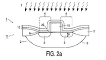
図2に示された実施形態では、半導体装置はMOSFET11である。この方法は、Si半導体ボディ2から始まり、これに、例えばポリシリコンで作られたnウェル16、アイソレーション17、ゲート誘電体25、およびゲート18が設けられている。これらはすべて、当業者に周知の方法で形成される。
In the embodiment shown in FIG. 2, the semiconductor device is a
放射のための吸収層10が、ゲート18を有する半導体ボディ2の表面6に設けられる。本実施形態では、248nmのレーザー放射のための吸収層10が、12nmのTEOSおよび20nmのTi/TiNの多層で形成される。この表面に、その後、放射パルス7が照射される。
An
図2aに示す実施形態においては、表面に、248nmのKrFエキシマーレーザーによって、50mJ/cm2のエネルギー密度で15psの間、照射が行われる。これにより、ソース12およびドレイン13領域が、15nmの深さ9まで非晶質化される。
In the embodiment shown in FIG. 2a, the surface is irradiated by a 248 nm KrF excimer laser at an energy density of 50 mJ / cm 2 for 15 ps. Thereby, the
図2bにおいて、その後、Ti/TiNの多層が除去される。Ti/TiNの多層は、例えば、フッ素を含む溶液での化学エッチング、あるいは、例えばHe/SF6のプラズマでのリアクティブイオンエッチングで除去される。 In FIG. 2b, the Ti / TiN multilayer is then removed. The multilayer of Ti / TiN is removed by, for example, chemical etching with a solution containing fluorine or reactive ion etching with, for example, He / SF 6 plasma.
重要なことは、注入の間に金属原子が半導体ボディ2に入ることを防ぐために、吸収層10を除去しなければならないことである。
What is important is that the
図2cにおいて、その後、ドーパント原子8が、非晶質表面層5に供給される。示された実施形態では、Bイオンが、0.5keVのエネルギーにより1×10¹⁵at/cm2のドーズで非晶質表面層5に注入される。例えばレジストなどの注入マスク19を使用して、B原子が、該当するp型トランジスタのソース12およびドレイン13領域のみに注入される。注入後、レジストマスク19が除去される。ドーパント原子は、急速熱アニーリング(RTA)処理で活性化される。
In FIG. 2 c,
半導体ボディ2は、RTAにおいて、いわゆるスパイクアニールによって急速に加熱され、その後実質的に直ちに再冷却される。示された実施形態では、B原子が1000℃で約1秒間加熱され、その後直ちに冷却される。
The
ドープp型領域3は、約15nmの深さを持つ。ドーピングプロファイルは、10あたり0.2nmの急激な傾斜を持つ。200オーム/平方の、比較的低いシート抵抗が、ほとんどすべてのB原子がSi格子内に置換的に存在し、適宜に電気的に活性化していることを示している。
The doped p-
注入ダメージにより起こるソース12およびドレイン13領域のBテールによる短チャネル効果の被害を大きく被るのは、特に、周知の方法で製造されたpチャネルMOSFETである。Bの一時的な拡散の増加が、比較的高温でのドーパント原子の活性化の間に生じ、Bテールの原因となる。この結果、急勾配のソースおよびドレイン接合は、周知の方法では良好に製造できない。対照的に、本発明に従う方法で製造されたソースおよびドレイン接合は、非常に浅い深さを有し、その結果、横向きの拡散も非常に少ない。これは、ソースおよびドレインがチャネルの長さに及ぼす影響を、比較的小さくする。短チャネル効果は、本発明に係る方法により減少される。本発明に係る方法は、したがって、概して40nmの非常に小さなチャネル長さを有するMOSFETに最適である。
In particular, p-channel MOSFETs manufactured by a well-known method are greatly damaged by the short channel effect caused by the B tails of the
あるいはまた、図3に示されるように、ソース12およびドレイン13接合に、非常に浅い深さと高度の活性化を有する拡張部を設けてもよい。ソースおよびドレイン拡張部20,21は、DIBL(Drain-Induced Barrier Lowering)等の短チャネル効果や突き抜けを最小にするためには、非常に重要である。この配列では、直列抵抗は、主にソースおよびドレイン拡張部に存在するが、より深いソース12およびドレイン13接合が最終的にシリサイド化され、直列抵抗を減少させる。
Alternatively, as shown in FIG. 3, the
非常に浅いソースおよびドレイン拡張部20,21は、短チャネル効果を抑制するのに有利であり、一方、高度の活性化は、MOSFETの直列抵抗の減少に貢献する。
Very shallow source and
図3aは、例えばRTAでのイオン注入および拡散により、より深いソース12およびドレイン13接合が製造される、当業者に周知のMOSFET処理から始まる。
FIG. 3a begins with a MOSFET process well known to those skilled in the art in which
任意に、ポケット22をイオン注入により設けてもよい。これらのポケット22は、トランジスタの動作中に、ソース12およびドレイン13接合の空乏領域の減少に役立つ。このため、ポケットのドーピングは一般により高く、また、ウェルのドーピング(この場合はn型)と同一のタイプである。
Optionally, the
図3bにおいて、スペーサ23が除去される。スペーサは、例えば、窒化シリコンにより作られ、H3PO4で化学的にエッチングすることが可能である。
In FIG. 3b, the
図3cにおいて、その後、12nmのTEOSと20nmのTi/TiNの多層とから成る吸収層10が設けられる。次に、浅いソースおよびドレイン拡張部20,21が、本発明に係る方法で形成される。上述の表面照射が使用される。これにより、非常に浅い深さ9を有する非晶質表面層5が作られる。
In FIG. 3c, an
吸収層10が除去され、直ちに、ソースおよびドレイン拡張部21,22ならびにゲート18が注入される(図3dを参照)。
Absorbing
ドーパント原子が、その後、上述の方法で、例えば急速熱アニーリングまたはレーザーアニーリングにより活性化される。 The dopant atoms are then activated in the manner described above, for example by rapid thermal annealing or laser annealing.
大きな利点は、ドーパント原子の非常に良好な活性化が、この最後の工程で得られ、その後の処理では、ドーパント原子の非活性化をもたらす比較的高熱の工程がそれ以上必要とされないことである。ドーパント原子の良好な活性化は、ソースおよびドレイン拡張部のシート抵抗と、ソースおよびドレインならびに多結晶シリコンの抵抗を比較的低くする。この結果、本発明に従って製造されたMOSFETのソースとドレインの間では、比較的大きな電流が流れる。 The great advantage is that very good activation of the dopant atoms is obtained in this last step, and subsequent processing does not require any further high-temperature steps leading to deactivation of the dopant atoms. . Good activation of the dopant atoms results in relatively low source and drain extension sheet resistance and source and drain and polycrystalline silicon resistance. As a result, a relatively large current flows between the source and drain of the MOSFET manufactured according to the present invention.
本発明は、上述の例に限定されず、すべてのタイプのダイオード、特に発光ダイオード(LED)、バイポーラトランジスタ、または、他のへテロ構造バイポーラトランジスタ、フラッシュやEEPROMなどのメモリセル等に、使用可能であることに留意されたい。また、本発明はp型トランジスタに限定されず、n型トランジスタに対しても、同等に好適に用いることができる。この方法はシリコンに限定されず、ゲルマニウム、ならびに、GeおよびSiを含む化合物に対しても用いることができる。 The present invention is not limited to the above examples, and can be used for all types of diodes, particularly light emitting diodes (LEDs), bipolar transistors, or other heterostructure bipolar transistors, memory cells such as flash and EEPROM, etc. Please note that. Further, the present invention is not limited to a p-type transistor, and can be equally suitably used for an n-type transistor. This method is not limited to silicon, but can also be used for germanium and compounds containing Ge and Si.
当業者には明らかなように、特定の実施形態における特定の寸法および材料は、変更が可能である。 As will be apparent to those skilled in the art, the specific dimensions and materials in specific embodiments can be varied.
Claims (12)
前記非晶質化は、前記表面への放射パルスの照射を通じて行われ、前記放射パルスは、前記放射パルスの放射が前記結晶表面領域に吸収されるような波長を有し、かつ、前記結晶表面層を溶解するようなエネルギー束を有する、ことを特徴とする製造方法。 A method of manufacturing a semiconductor device having a semiconductor body, wherein a doped region is formed in the semiconductor body, the semiconductor body comprises a crystalline semiconductor surface region of a semiconductor material, and at least a part of the crystalline semiconductor surface region is amorphous. In the manufacturing method of forming an amorphous surface layer by converting into
The amorphization is performed through irradiation of the surface with a radiation pulse, the radiation pulse having a wavelength such that the radiation pulse radiation is absorbed by the crystal surface region, and the crystal surface A manufacturing method characterized by having an energy flux that dissolves the layer.
前記ドーパント原子が、格子サイトに置換的に組み込まれ、これにより前記ドーパント原子が活性化される、ことを特徴とする請求項3に記載の方法。 The amorphous surface layer is heated to a temperature lower than the melting temperature of the amorphous semiconductor material by rapid thermal annealing (RTA) to recrystallize the amorphous surface layer,
The method of claim 3, wherein the dopant atoms are substituted into lattice sites and thereby activate the dopant atoms.
前記非晶質半導体表面層は、前記MOSFETのソースまたはドレインの形成に用いられる、ことを特徴とする請求項1に記載の方法。 MOSFET is formed,
The method of claim 1, wherein the amorphous semiconductor surface layer is used to form a source or drain of the MOSFET.
Applications Claiming Priority (2)
| Application Number | Priority Date | Filing Date | Title |
|---|---|---|---|
| EP01204625 | 2001-11-30 | ||
| PCT/IB2002/004881 WO2003046967A2 (en) | 2001-11-30 | 2002-11-20 | Method of forming a doped region in a semiconductor body comprising a step of amorphization by irradiation |
Publications (2)
| Publication Number | Publication Date |
|---|---|
| JP2005510871A true JP2005510871A (en) | 2005-04-21 |
| JP2005510871A5 JP2005510871A5 (en) | 2006-01-12 |
Family
ID=8181336
Family Applications (1)
| Application Number | Title | Priority Date | Filing Date |
|---|---|---|---|
| JP2003548292A Pending JP2005510871A (en) | 2001-11-30 | 2002-11-20 | Manufacturing method of semiconductor device |
Country Status (7)
| Country | Link |
|---|---|
| US (1) | US6982212B2 (en) |
| EP (1) | EP1459366A2 (en) |
| JP (1) | JP2005510871A (en) |
| KR (1) | KR20040054811A (en) |
| AU (1) | AU2002348835A1 (en) |
| TW (1) | TWI268576B (en) |
| WO (1) | WO2003046967A2 (en) |
Cited By (5)
| Publication number | Priority date | Publication date | Assignee | Title |
|---|---|---|---|---|
| JP2009529245A (en) * | 2006-03-08 | 2009-08-13 | アプライド マテリアルズ インコーポレイテッド | Method and apparatus for heat treatment structure formed on a substrate |
| JP2013128030A (en) * | 2011-12-19 | 2013-06-27 | Sanken Electric Co Ltd | Semiconductor device manufacturing method and semiconductor device |
| JP2014060423A (en) * | 2006-03-08 | 2014-04-03 | Applied Materials Inc | Method and device for heat treated structure formed on substrate |
| JP2018032786A (en) * | 2016-08-25 | 2018-03-01 | パナソニックIpマネジメント株式会社 | Solar cell and manufacturing method thereof |
| KR20190015262A (en) * | 2016-05-31 | 2019-02-13 | 레이저 시스템즈 앤드 솔루션즈 오브 유럽 | Diaphragm junction electronic device and manufacturing process thereof |
Families Citing this family (18)
| Publication number | Priority date | Publication date | Assignee | Title |
|---|---|---|---|---|
| JP3737504B2 (en) * | 2004-03-31 | 2006-01-18 | 松下電器産業株式会社 | Manufacturing method of semiconductor device |
| FR2870988B1 (en) * | 2004-06-01 | 2006-08-11 | Michel Bruel | METHOD FOR MAKING A MULTI-LAYER STRUCTURE COMPRISING, IN DEPTH, A SEPARATION LAYER |
| JP2006066686A (en) * | 2004-08-27 | 2006-03-09 | Matsushita Electric Ind Co Ltd | Method and apparatus for introducing impurities |
| US7091097B1 (en) * | 2004-09-03 | 2006-08-15 | Advanced Micro Devices, Inc. | End-of-range defect minimization in semiconductor device |
| US7615502B2 (en) * | 2005-12-16 | 2009-11-10 | Sandisk 3D Llc | Laser anneal of vertically oriented semiconductor structures while maintaining a dopant profile |
| KR100732630B1 (en) * | 2006-02-01 | 2007-06-27 | 삼성전자주식회사 | Semiconductor devices including impurity doped region and methods of forming the same |
| US7679166B2 (en) * | 2007-02-26 | 2010-03-16 | International Business Machines Corporation | Localized temperature control during rapid thermal anneal |
| US7759773B2 (en) | 2007-02-26 | 2010-07-20 | International Business Machines Corporation | Semiconductor wafer structure with balanced reflectance and absorption characteristics for rapid thermal anneal uniformity |
| US7692275B2 (en) * | 2007-02-26 | 2010-04-06 | International Business Machines Corporation | Structure and method for device-specific fill for improved anneal uniformity |
| US20090096066A1 (en) * | 2007-10-10 | 2009-04-16 | Anderson Brent A | Structure and Method for Device-Specific Fill for Improved Anneal Uniformity |
| US7745909B2 (en) * | 2007-02-26 | 2010-06-29 | International Business Machines Corporation | Localized temperature control during rapid thermal anneal |
| US8138066B2 (en) | 2008-10-01 | 2012-03-20 | International Business Machines Corporation | Dislocation engineering using a scanned laser |
| CA2962682C (en) | 2009-03-09 | 2019-11-26 | 1366 Technologies Inc. | Methods and apparati for making thin semiconductor bodies from molten material |
| GB201112610D0 (en) * | 2011-07-22 | 2011-09-07 | Rec Wafer Norway As | Heating a furnace for the growth of semiconductor material |
| US9597744B2 (en) * | 2013-11-11 | 2017-03-21 | Siemens Energy, Inc. | Method for utilizing a braze material with carbon structures |
| DE102016114264A1 (en) * | 2016-08-02 | 2018-02-08 | Infineon Technologies Ag | METHOD OF MANUFACTURING INCLUDING AN ACTIVATION OF DOPING MATERIALS AND SEMICONDUCTOR SEMICONDUCTORS |
| CN108807276A (en) * | 2017-05-05 | 2018-11-13 | 中芯国际集成电路制造(上海)有限公司 | Semiconductor structure and forming method thereof |
| CN112885715A (en) * | 2021-01-08 | 2021-06-01 | 中国科学院微电子研究所 | Method for manufacturing semiconductor device |
Family Cites Families (5)
| Publication number | Priority date | Publication date | Assignee | Title |
|---|---|---|---|---|
| US4535220A (en) * | 1981-11-10 | 1985-08-13 | The Secretary Of State For Defence In Her Britannic Majesty's Government Of The United Kingdom Of Great Britain And Northern Ireland | Integrated circuits |
| JPH01256124A (en) * | 1988-04-05 | 1989-10-12 | Ricoh Co Ltd | Manufacture of mos type semiconductor device |
| US5950078A (en) * | 1997-09-19 | 1999-09-07 | Sharp Laboratories Of America, Inc. | Rapid thermal annealing with absorptive layers for thin film transistors on transparent substrates |
| US5953615A (en) | 1999-01-27 | 1999-09-14 | Advance Micro Devices | Pre-amorphization process for source/drain junction |
| US6777317B2 (en) * | 2001-08-29 | 2004-08-17 | Ultratech Stepper, Inc. | Method for semiconductor gate doping |
-
2002
- 2002-11-20 EP EP02781567A patent/EP1459366A2/en not_active Withdrawn
- 2002-11-20 AU AU2002348835A patent/AU2002348835A1/en not_active Abandoned
- 2002-11-20 US US10/497,263 patent/US6982212B2/en not_active Expired - Fee Related
- 2002-11-20 KR KR10-2004-7008218A patent/KR20040054811A/en not_active Application Discontinuation
- 2002-11-20 JP JP2003548292A patent/JP2005510871A/en active Pending
- 2002-11-20 WO PCT/IB2002/004881 patent/WO2003046967A2/en active Application Filing
- 2002-11-26 TW TW091134323A patent/TWI268576B/en not_active IP Right Cessation
Cited By (10)
| Publication number | Priority date | Publication date | Assignee | Title |
|---|---|---|---|---|
| JP2009529245A (en) * | 2006-03-08 | 2009-08-13 | アプライド マテリアルズ インコーポレイテッド | Method and apparatus for heat treatment structure formed on a substrate |
| JP2014060423A (en) * | 2006-03-08 | 2014-04-03 | Applied Materials Inc | Method and device for heat treated structure formed on substrate |
| US10141191B2 (en) | 2006-03-08 | 2018-11-27 | Applied Materials, Inc. | Method of thermal processing structures formed on a substrate |
| US10840100B2 (en) | 2006-03-08 | 2020-11-17 | Applied Materials, Inc. | Method of thermal processing structures formed on a substrate |
| JP2013128030A (en) * | 2011-12-19 | 2013-06-27 | Sanken Electric Co Ltd | Semiconductor device manufacturing method and semiconductor device |
| KR20190015262A (en) * | 2016-05-31 | 2019-02-13 | 레이저 시스템즈 앤드 솔루션즈 오브 유럽 | Diaphragm junction electronic device and manufacturing process thereof |
| JP2019523986A (en) * | 2016-05-31 | 2019-08-29 | レーザー システムズ アンド ソリューションズ オブ ヨーロッパ | Deep junction electronic device and method of manufacturing the same |
| KR102478873B1 (en) | 2016-05-31 | 2022-12-19 | 레이저 시스템즈 앤드 솔루션즈 오브 유럽 | DIP junction electronic device and its manufacturing process |
| JP2018032786A (en) * | 2016-08-25 | 2018-03-01 | パナソニックIpマネジメント株式会社 | Solar cell and manufacturing method thereof |
| WO2018037751A1 (en) * | 2016-08-25 | 2018-03-01 | パナソニックIpマネジメント株式会社 | Solar cell and method for manufacturing same |
Also Published As
| Publication number | Publication date |
|---|---|
| EP1459366A2 (en) | 2004-09-22 |
| TW200409293A (en) | 2004-06-01 |
| KR20040054811A (en) | 2004-06-25 |
| WO2003046967A2 (en) | 2003-06-05 |
| WO2003046967A3 (en) | 2003-10-16 |
| US6982212B2 (en) | 2006-01-03 |
| AU2002348835A1 (en) | 2003-06-10 |
| US20050003638A1 (en) | 2005-01-06 |
| TWI268576B (en) | 2006-12-11 |
Similar Documents
| Publication | Publication Date | Title |
|---|---|---|
| US6982212B2 (en) | Method of manufacturing a semiconductor device | |
| JP2005510871A5 (en) | ||
| US6380044B1 (en) | High-speed semiconductor transistor and selective absorption process forming same | |
| US6365476B1 (en) | Laser thermal process for fabricating field-effect transistors | |
| US6936505B2 (en) | Method of forming a shallow junction | |
| US7825016B2 (en) | Method of producing a semiconductor element | |
| KR100511765B1 (en) | Fabrication mehtod for reduced-dimension integrated circuits | |
| KR100879494B1 (en) | Method for semiconductor gate doping | |
| US6645838B1 (en) | Selective absorption process for forming an activated doped region in a semiconductor | |
| JPH0669149A (en) | Fabrication of semiconductor device | |
| US6555439B1 (en) | Partial recrystallization of source/drain region before laser thermal annealing | |
| US20020192914A1 (en) | CMOS device fabrication utilizing selective laser anneal to form raised source/drain areas | |
| US20070281472A1 (en) | Method of increasing transistor performance by dopant activation after silicidation | |
| US7112499B2 (en) | Dual step source/drain extension junction anneal to reduce the junction depth: multiple-pulse low energy laser anneal coupled with rapid thermal anneal | |
| JP2010021525A (en) | Manufacturing method for semiconductor device | |
| US20070232033A1 (en) | Method for forming ultra-shallow high quality junctions by a combination of solid phase epitaxy and laser annealing | |
| US7615458B2 (en) | Activation of CMOS source/drain extensions by ultra-high temperature anneals | |
| JP2008510300A (en) | Ultra shallow junction formation method | |
| CN1316569C (en) | Low-temperature post-dopant activation process | |
| US6952269B2 (en) | Apparatus and method for adiabatically heating a semiconductor surface | |
| JP2005101196A (en) | Method of manufacturing semiconductor integrated circuit device | |
| Schmidt et al. | Materials processing | |
| US7091097B1 (en) | End-of-range defect minimization in semiconductor device | |
| JP2002246329A (en) | Formation method for very shallow p-n junction of semiconductor substrate | |
| JPH0677155A (en) | Heat treatment method for semiconductor substrate |
Legal Events
| Date | Code | Title | Description |
|---|---|---|---|
| A521 | Written amendment |
Free format text: JAPANESE INTERMEDIATE CODE: A523 Effective date: 20051118 |
|
| A621 | Written request for application examination |
Free format text: JAPANESE INTERMEDIATE CODE: A621 Effective date: 20051118 |
|
| A711 | Notification of change in applicant |
Free format text: JAPANESE INTERMEDIATE CODE: A711 Effective date: 20080612 |
|
| A977 | Report on retrieval |
Free format text: JAPANESE INTERMEDIATE CODE: A971007 Effective date: 20080718 |
|
| A131 | Notification of reasons for refusal |
Free format text: JAPANESE INTERMEDIATE CODE: A131 Effective date: 20080805 |
|
| A521 | Written amendment |
Free format text: JAPANESE INTERMEDIATE CODE: A523 Effective date: 20081017 |
|
| A02 | Decision of refusal |
Free format text: JAPANESE INTERMEDIATE CODE: A02 Effective date: 20090327 |