JP2005509890A - Method and apparatus for measuring waveforms - Google Patents
Method and apparatus for measuring waveforms Download PDFInfo
- Publication number
- JP2005509890A JP2005509890A JP2003546119A JP2003546119A JP2005509890A JP 2005509890 A JP2005509890 A JP 2005509890A JP 2003546119 A JP2003546119 A JP 2003546119A JP 2003546119 A JP2003546119 A JP 2003546119A JP 2005509890 A JP2005509890 A JP 2005509890A
- Authority
- JP
- Japan
- Prior art keywords
- waveform
- frequency
- gated
- time point
- signal
- Prior art date
- Legal status (The legal status is an assumption and is not a legal conclusion. Google has not performed a legal analysis and makes no representation as to the accuracy of the status listed.)
- Pending
Links
- 238000000034 method Methods 0.000 title claims description 65
- 238000005259 measurement Methods 0.000 claims abstract description 163
- 238000005070 sampling Methods 0.000 claims abstract description 40
- 239000000835 fiber Substances 0.000 claims abstract description 24
- 230000003287 optical effect Effects 0.000 claims description 48
- 238000011084 recovery Methods 0.000 claims description 21
- 230000003252 repetitive effect Effects 0.000 claims description 16
- 230000002159 abnormal effect Effects 0.000 claims description 13
- 230000005856 abnormality Effects 0.000 claims description 10
- 238000012545 processing Methods 0.000 claims description 10
- 230000001902 propagating effect Effects 0.000 claims description 3
- 230000007704 transition Effects 0.000 claims 2
- 230000003111 delayed effect Effects 0.000 claims 1
- 238000004458 analytical method Methods 0.000 description 18
- 230000006870 function Effects 0.000 description 18
- 238000006243 chemical reaction Methods 0.000 description 17
- 238000004891 communication Methods 0.000 description 16
- 230000008859 change Effects 0.000 description 15
- 230000007274 generation of a signal involved in cell-cell signaling Effects 0.000 description 15
- 239000003550 marker Substances 0.000 description 13
- 238000010586 diagram Methods 0.000 description 6
- 238000011156 evaluation Methods 0.000 description 6
- 238000012937 correction Methods 0.000 description 5
- 230000002547 anomalous effect Effects 0.000 description 4
- 230000005540 biological transmission Effects 0.000 description 4
- 230000008569 process Effects 0.000 description 4
- 230000000007 visual effect Effects 0.000 description 4
- 238000004590 computer program Methods 0.000 description 3
- 238000012986 modification Methods 0.000 description 3
- 230000004048 modification Effects 0.000 description 3
- 230000000737 periodic effect Effects 0.000 description 3
- 230000004044 response Effects 0.000 description 3
- 238000004364 calculation method Methods 0.000 description 2
- 238000013461 design Methods 0.000 description 2
- 230000001052 transient effect Effects 0.000 description 2
- 229910052691 Erbium Inorganic materials 0.000 description 1
- 230000009471 action Effects 0.000 description 1
- 230000004913 activation Effects 0.000 description 1
- 238000003491 array Methods 0.000 description 1
- 230000009286 beneficial effect Effects 0.000 description 1
- 230000008901 benefit Effects 0.000 description 1
- 238000004883 computer application Methods 0.000 description 1
- 238000013500 data storage Methods 0.000 description 1
- 238000005516 engineering process Methods 0.000 description 1
- UYAHIZSMUZPPFV-UHFFFAOYSA-N erbium Chemical compound [Er] UYAHIZSMUZPPFV-UHFFFAOYSA-N 0.000 description 1
- 230000010354 integration Effects 0.000 description 1
- 230000001788 irregular Effects 0.000 description 1
- GQYHUHYESMUTHG-UHFFFAOYSA-N lithium niobate Chemical compound [Li+].[O-][Nb](=O)=O GQYHUHYESMUTHG-UHFFFAOYSA-N 0.000 description 1
- 230000005389 magnetism Effects 0.000 description 1
- 230000007246 mechanism Effects 0.000 description 1
- 229910052761 rare earth metal Inorganic materials 0.000 description 1
- 150000002910 rare earth metals Chemical class 0.000 description 1
- 230000009131 signaling function Effects 0.000 description 1
- 230000003068 static effect Effects 0.000 description 1
- 230000001360 synchronised effect Effects 0.000 description 1
- 238000012360 testing method Methods 0.000 description 1
- 230000009466 transformation Effects 0.000 description 1
- 230000001960 triggered effect Effects 0.000 description 1
Images


Classifications
-
- G—PHYSICS
- G01—MEASURING; TESTING
- G01J—MEASUREMENT OF INTENSITY, VELOCITY, SPECTRAL CONTENT, POLARISATION, PHASE OR PULSE CHARACTERISTICS OF INFRARED, VISIBLE OR ULTRAVIOLET LIGHT; COLORIMETRY; RADIATION PYROMETRY
- G01J11/00—Measuring the characteristics of individual optical pulses or of optical pulse trains
-
- G—PHYSICS
- G01—MEASURING; TESTING
- G01R—MEASURING ELECTRIC VARIABLES; MEASURING MAGNETIC VARIABLES
- G01R23/00—Arrangements for measuring frequencies; Arrangements for analysing frequency spectra
- G01R23/16—Spectrum analysis; Fourier analysis
- G01R23/165—Spectrum analysis; Fourier analysis using filters
-
- G—PHYSICS
- G01—MEASURING; TESTING
- G01R—MEASURING ELECTRIC VARIABLES; MEASURING MAGNETIC VARIABLES
- G01R29/00—Arrangements for measuring or indicating electric quantities not covered by groups G01R19/00 - G01R27/00
- G01R29/26—Measuring noise figure; Measuring signal-to-noise ratio
Abstract
システムは、ゲート制御の値により波形のセグメントを分離してそのセグメントを測定する。波形の異常がゲート処理される。ゲート処理された波形は、多数の周波数抽出器に供給され、そこでゲート処理された波形の個々の周波数での周波数内容についての情報を生成する。ゲート処理された波形に導入された歪が、基準波形に同じゲート制御を適用することにより測定される。システムは、入力波形から復元されたクロック信号により指示された時間間隔で入力波形を測定またはゲート制御する。測定されるべき波形のセグメントは、ファイバーループを通じて循環され、循環される信号のセグメントは、各循環において、測定システムに与えるために分割される。波形がしきい値とクロスする時間ポイントはストラドルサンプリングにより決定される。 The system separates the waveform segments by the gate control value and measures the segments. Waveform anomalies are gated. The gated waveform is fed to a number of frequency extractors where it generates information about the frequency content at the individual frequencies of the gated waveform. The distortion introduced into the gated waveform is measured by applying the same gate control to the reference waveform. The system measures or gates the input waveform at time intervals indicated by a clock signal recovered from the input waveform. The segment of the waveform to be measured is circulated through the fiber loop, and the segment of the signal to be circulated is split in each cycle for feeding to the measurement system. The time point at which the waveform crosses the threshold is determined by straddle sampling.
Description
この発明は信号解析のための装置に関する。別の態様では、この発明は信号を解析するための方法に関する。 The present invention relates to an apparatus for signal analysis. In another aspect, the invention relates to a method for analyzing a signal.
多くの電子回路設計は、データ通信経路の設計および命令を扱わなくてはならない。通信経路がパソコンのメモリとマイクロプロセッサとの間にあるか、あるいはそれが海底光通信リンクの二つの終端ノードとの間にあるかによって、信号強度が重要となる。波形解析装置は、これらの通信経路に対し送受信された波形の振幅を測定するために用いられる。典型的には、この装置は、波形の振幅を時間の関数として、再現するために参考となる時間および振幅に関連して、ある種の振幅および時間のサンプリングを利用する。結果、得られた波形はこれらの送信経路およびデータを送信する能力の特性を決定するために用いられる。 Many electronic circuit designs must deal with data communication path design and instructions. The signal strength is important depending on whether the communication path is between the memory of the personal computer and the microprocessor, or between the two end nodes of the submarine optical communication link. The waveform analyzer is used to measure the amplitude of the waveform transmitted / received to / from these communication paths. Typically, this device utilizes some kind of amplitude and time sampling in relation to the time and amplitude that are referenced to reproduce the amplitude of the waveform as a function of time. As a result, the resulting waveform is used to determine the characteristics of these transmission paths and the ability to transmit data.
二つの顕著なサンプリング波形は、時間変数での電気および光信号に関する波形を測定するために産業上で用いられる。一つの方法は、予め決められた波形振幅に達した時に、時間を測定する。他の方法は、予め決められた時間で振幅を測定する。両方法は、測定毎の波形に関係した個別の時間−振幅値のペアを呈する。両方法の目標は、瞬時の測定を行うことである。即ち、測定のために波形が考慮される、時間または振幅の期間は、測定エラーを回避するために極力小さくする。許容できる時間および振幅の期間は、時間に対する波形振幅の変更速度により抑制される。 Two prominent sampling waveforms are used in the industry to measure waveforms related to electrical and optical signals in time variables. One method measures time when a predetermined waveform amplitude is reached. Another method measures the amplitude at a predetermined time. Both methods present individual time-amplitude value pairs related to the waveform for each measurement. The goal of both methods is to make instantaneous measurements. That is, the time or amplitude period in which the waveform is taken into account for measurement is made as small as possible to avoid measurement errors. Allowable time and amplitude periods are constrained by the rate of change of the waveform amplitude with respect to time.
波形は、時間的な連続した測定を採取する(シーケンシャル・サンプリング)ことにより、表すことができる。もし、測定が実行される速度が、波形の変化速度よりも速いなら、波形の良好な再現が行える。しかしながら、もし、波形が変化する速度が、測定システムの測定速度と同速度または速い場合、波形の良好な再現は達成できない。 The waveform can be represented by taking successive measurements in time (sequential sampling). If the speed at which the measurement is performed is faster than the waveform change rate, a good reproduction of the waveform can be achieved. However, if the speed at which the waveform changes is the same or faster than the measurement speed of the measurement system, good reproduction of the waveform cannot be achieved.
周期性または反復性の波形の場合、波形再現に他の方法を採用できる。その方法は通常、トリガー発生後の種々の時間にて、測定を行うことを含む、反復性サンプリングに関する。 For periodic or repetitive waveforms, other methods can be employed for waveform reproduction. The method usually relates to repetitive sampling, which includes taking measurements at various times after the trigger occurs.
このトリガー発生は、周期性波形の反復速度で起きる出来事である。時間の計画値が命令され、その計画に基づき、一つのトリガー発生に対応する一つの測定に対して測定が実行される。時間および振幅測定の対応するテーブルは、波形の再現を与える。 This trigger occurrence is an event that occurs at the repetition rate of the periodic waveform. A planned value of time is commanded, and based on the plan, a measurement is performed for one measurement corresponding to one trigger occurrence. Corresponding tables of time and amplitude measurements give waveform reproduction.
この発明は、波形を測定するための方法および装置に適用できるようにされている。しかしこの発明はそのように限定されず、この発明の種々の態様への適用が以下に示した実施例の論議を通じて得られるであろう。 The present invention can be applied to a method and an apparatus for measuring a waveform. However, the invention is not so limited and application to various aspects of the invention will be gained through a discussion of the examples presented below.
波形を測定するための方法および装置は、信号が反復性または非反復性の時に関連した状況に対して与えられる。波形は信号、光学的、電気的、または別の方法であってもよく、これらは時間の関数として変化する振幅を有する。その波形は特徴を含む。特徴は、波形の質あるいは特性に関連づけられるような重要性であると考えられる、一時的に別個の出来事である。特徴は、各適用のために、時間についての最適な振幅等高線を持つことである。特徴の例は、オーバーシュート、プリシュート、リンギング、キャリアの位相または周波数での変化、特定しきい値電圧にクロスする信号などを一つのローカル状態から他へ転位できることである。複数の特徴および複数の特徴間の関係は、波形解析で重大関心事である。測定は、最小のデータ取得であり、そのことによって、波形についてのいくつかの情報が得られる。例は、アナログからデジタル変換への単一の振幅変換であり、波形の1ポイントまたは一つの時間測定が得られる。 Methods and apparatus for measuring waveforms are provided for situations related when the signal is repetitive or non-repetitive. The waveform may be signal, optical, electrical, or another method, which has an amplitude that varies as a function of time. The waveform includes features. A feature is a temporally separate event that may be of importance as related to the quality or characteristics of the waveform. The feature is to have an optimal amplitude contour over time for each application. Examples of features are that overshoot, preshoot, ringing, changes in carrier phase or frequency, signals that cross a particular threshold voltage, etc. can be transposed from one local state to another. Features and relationships between features are a major concern in waveform analysis. A measurement is a minimal data acquisition, which gives some information about the waveform. An example is a single amplitude conversion from analog to digital conversion, resulting in one point or one time measurement of the waveform.
例示的な波形測定システム100が図0に示される。この発明の種々の実施例に基づく波形測定での初期のステップは、小さいが瞬間的でない期間の時間に対する考慮下で、波形の一部に対してサンプリングするか、ゲート処理する。時間ウインドウをゲート処理するかサンプリングする期間は関心のある特徴の期間である。測定されるべき波形は、タイミング発生回路12の制御により、ゲート制御機能10に送出される。タイミング発生回路12は、1ビットクロックのような内部信号(図示)または外部信号(不図示)によりイネーブルできる。波形のゲート処理は、シリアルデータ認識回路およびビットクロック回復回路を含む同期化回路を用いて波形と同期できる。他のタイプのトリガーおよび時間をベースにした回路を使用できる。
An exemplary
ゲート処理された後の波形は、1つ以上の周波数サンプリングブロック14により、周波数範囲内でサンプリングされる。その周波数サンプリングブロック14は、周波数f0のサンプリングチャンネル16、周波数f1のサンプリングチャンネル18、周波数fnのサンプリングチャンネル20を有する。一つの振幅、一連の振幅または種々の周波数成分の振幅および位相がその後に決定できる。決定されなくてはならない周波数成分の個数は、実行される解析のタイプに基づく。
The gated waveform is sampled within a frequency range by one or more
周波数f0〜fnは、ゲート制御機能10の期間に基づく。例えば、f0〜fnは、ゲート処理期間の逆数以下、またはそれに等しい高調波の周波数である。この構成は、ゲート処理された波形が再構築されるためのフーリエ係数となるためにシステムが用いられるならば、特に有用である。フーリエ解析は、ゲート処理された波形の再構築のための多くのスキームの内の単に一つである。従って、周波数f0〜fnは均一に離隔される必要はない。もし周波数サンプリングチャンネルが帯域パスフィルタの形態をとる場合、各周波数サンプリングチャンネル(ここでは“周波数情報抽出器”として参照される)が実際に周波数帯域に関する情報を生じると仮定すると、各周波数帯域は、同じ帯域でなくてはならない。最後に、各周波数サンプリングチャンネルが、正弦曲線以外の基本的な関数に関して、ゲート処理された波形についての振幅および位相情報を与えてもよい。例えば、周波数サンプリングバンク14は、ウェーブレット(wavelet)の基本的な関数を使用するように設計されてもよい。
The frequencies f 0 to f n are based on the period of the
これらの周波数成分が一旦、決定されると、ゲート処理される波形の部分は、プロセッサ22により実行できるソフトウエアにより、逆フーリエ変換のごとき変換を通じて数学的に再構築できる。広く言えば、周波数サンプリングバンク14により生成された情報は、時間を基礎とする関数(これはゲート処理された波形を再構築する)となるように用いることができる。一般に、結果となる測定値は、一つの時間での出来事に対する逆フーリエ変換である。結果となる再構築された波形は、ゲート処理またはサンプリングする期間に対する元の波形の全体の部分を示す。この信号は、前述した時間に基づく関数で議論したように、多数の時間の値を用いることにより、および、時間を表す軸に対するこのような計算の結果をプロットすることにより、図式的に復元されてもよい。
Once these frequency components are determined, the portion of the waveform to be gated can be mathematically reconstructed through a transformation, such as an inverse Fourier transform, by software that can be executed by the processor 22. Broadly speaking, the information generated by the
データ通信のコンテキストにおいて、一つのユニット・インターバル(UI)時間は、1ビットの情報を送出するために要求される時間の合計を示す。この発明のいくつかの実施例では、波長の一つのUIセグメントを測定できる。他の実施例では、多少のUIを測定できる。ゲート制御機能は、測定されるべきゲート処理するパルスおよび波長の乗算になる波長を生成する。得られた波長は、周波数分解チャンネルのバンクに供給され、そこで、周波数成分の振幅、または振幅および位相が評価される。これは、振幅検出器、直交検出器、デジタル信号処理または他の既知の技術により実行される。 In the context of data communication, one unit interval (UI) time indicates the total time required to send 1 bit of information. In some embodiments of the invention, one UI segment of wavelength can be measured. In other embodiments, some UI can be measured. The gating function generates a wavelength that is a multiplication of the gating pulse to be measured and the wavelength. The resulting wavelength is fed to a bank of frequency resolving channels where the amplitude, or amplitude and phase, of the frequency component is evaluated. This is performed by an amplitude detector, quadrature detector, digital signal processing or other known techniques.
ほぼ一つのUI幅である、ゲート処理する波長は、データ通信システムにおけるシリアルデータを発生するために用いられたものに似た回路を用いることができる。また、いくつかの実施例では、ゲート信号回路のエラーは、時間測定エラーに加算されない。この発明に基づく測定装置は、タイムウインドウ内の全体の特徴の取得を可能にする。 The gate processing wavelength, which is approximately one UI width, can use a circuit similar to that used to generate serial data in a data communication system. Also, in some embodiments, gate signal circuit errors are not added to time measurement errors. The measuring device according to the invention makes it possible to obtain the entire characteristics within the time window.
データ通信信号のコンテキストおよび、過渡的な“一つの時間”の出来事が重大関心事である波長ジッター測定において、波形の1ポイントよりも、波長の一部を測定できることが望ましい。波長の位置を測定できる能力は、信号の質および最終的なビットエラー率に関する重要な特性を決定するのに必要となる情報のすべてを提供する。 It is desirable to be able to measure a portion of the wavelength rather than one point in the waveform in the context of data communication signals and wavelength jitter measurements where transient “one-time” events are of great interest. The ability to measure wavelength location provides all of the information needed to determine important characteristics regarding signal quality and final bit error rate.
通信システムのビットエラー率は、送出されたデータビット数に起きたビットエラーの比率であり、システムがうまく動作しているかの基本的な指標となる。ビットエラー率の予測および評価は、データ通信での設備のテストのための重要な適用となる。 The bit error rate of a communication system is a ratio of bit errors occurring in the number of transmitted data bits, and is a basic indicator of whether the system is operating properly. Bit error rate prediction and evaluation is an important application for testing equipment in data communications.
通信チャンネルの端部での受信器は、到来するデータ流を一つのUIの基礎に基づき評価する。連続するデータ通信のための広く使用される分析形式である視覚による図は、一つのUI時間の期間上に、データ波形でのすべてのデータ変化を重ねることにより、時間が統一されたデータ変化の視覚を出力する。多くのビットエラー率の解析方法は、時間を標準化する。 The receiver at the end of the communication channel evaluates the incoming data stream on the basis of one UI. A visual diagram, a widely used form of analysis for continuous data communication, is the integration of time-varying data changes by overlaying all data changes in the data waveform over one UI time period. Output visual. Many bit error rate analysis methods standardize time.
波形測定システム100の実施例は、ビットエラー率の解析のためのアプリケーションをサポートするために使用できる、いくつかの異なるタイプの評価を出力する。データ変化が生じる位置、および振幅、タイミング・ジッターは、システムのビットエラー率を予測するために用いることができる。一つのカコデリは、いくつかの理想的な期待される輪郭に典型的に関連する単一の特徴の輪郭に関する特徴評価である。更に、オーバーシュート/プリシュート、変化時間および振幅が一つの測定で得られるので、評価は、極めて正確にできる。別の評価のカテゴリは、相対的な特徴解析である。これは、複数の特徴評価およびそれらが互いにどのようにして関係するかを含む。視覚による図は、データ波形が一つのUI時間の期間に関連して表示される相対特徴解析の一例である。視覚による図を用いるための一つの方法は、データ流内の変化を互いのトップにスーパーインポーズすることである。
Embodiments of the
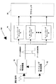
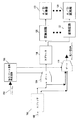
図1は、この発明に基づく例示的な波形測定システム100である。波形測定システム100は、スプリッタ104およびタイミング発生回路12を含む。そのタイミング発生回路は、シリアルデータマーカー発生回路106、クロック復元回路108、周波数測定回路109および指令/ゲート信号発生回路110を含む。この波形測定システムは、ゲート114および116、スプリッタ118、変換回路120、121および、アナログ・デジタル変換回路112、123を含む。データ信号102は、スプリッタ104に供給される。スプリッタ104は、高帯域スプリッタ、フィルタおよびアンプを含む。この実施例では、スプリッタ104は、入力信号102を4つのチャンネルに分割し、各チャンネルはシリアルデータマッカー発生回路106、クロック復元回路108およびゲート114、116に器与えられる。ゲート114、116は通常、FETまたはダイオードブリッジである。
FIG. 1 is an exemplary
シリアルデータマーカー発生回路106は、トリガーを出力して波形の特定の部位を観察できるように、データ信号102を認識する。これは多種の方法で実行できる。図2は、この発明の1実施例に基づくシリアルデータマーカー発生回路106の一例を示す。もし、シリアルデータが反復パターンであり、そしてパターン長が既知ならば、ビットクロックで動作するカウンタ200は、各パターンで同じ時間に起きる、出来事(マーカー)を作成するようにセットされ得る。図3は、この発明の別の実施例に基づくシリアルデータマーカー発生回路106の一例を示す。回路106は、シフトレジスタ300、レジスタ302およびコンパレータ304を含む。入力データはシフトレジスタ300に供給され、そのレジスタ300はビットクロックによりトリガーされる。コンパレータ304は、シフトレジスタ300に格納されたデータをレジスタ302に格納されたデータと比較し、一致した時にマーカーを出力する。
The serial data
パターン同期化の機能性は、多くの形態をとることができる。パターン長がロードされ、復元されるビットクロックによりクロック制御されるプログラム可能なカウンタを極力簡単にできる。末端カウンタであるこのカウンタは、パターンを追跡できるパターンマーカーを提供する。この構成は、クロック解析を含む適用に有用である。カウンタの出力部でのデジタルカウンタは、パターン内の異なるビット位置で測定を初期化するための時間オフセットを発生するために用いられる。データ流比較機能は、可変長の比較に基づく測定を許可するという点で、より大きい機能性を許可する。 The functionality of pattern synchronization can take many forms. A programmable counter that is clocked by the bit clock loaded with the pattern length and restored can be simplified as much as possible. This counter, which is an end counter, provides a pattern marker that can track the pattern. This configuration is useful for applications involving clock analysis. A digital counter at the output of the counter is used to generate a time offset to initialize the measurement at different bit positions in the pattern. The data stream comparison function allows greater functionality in that it allows measurements based on variable length comparisons.
いくつかの実施例では、クロック復元回路108は、入力データ信号からビットクロックを復元する。他の実施例では、ビットクロックは復元されない。このビットクロックは、波形測定を可能にするために用いられる。図4は、この発明に基づくビット復元回路の一例を示す。そのビットクロック復元回路108は、変化検出器400およびPLL410を含む。変化検出器400は、データの各変化でパルスを出力する。PLL410は、位相検出器402、ローパスフィルタ404および電圧制御の発振器(VCO)408を含む。入力データは、PLL410に結合された変化検出器400に与えられる。
In some embodiments, the
ビットクロックは、設定により、一つのUI期間を持つ。そのビットクロックは、データ波形をサンプリングしてデータを受信するための受信器により用いられる時間ベースである。ビットクロックとデータとの関係は、他のファクタと共に、システムのビットエラー率を最終的に決定するものである。データ流に対するビットクロックをトラックする高いクォリティのクロックを発生できるなら、そのクロックはデータ波形の測定を行うためのシステムで用いることができる。測定の動作が一つのUI期間に直接に関係するので、復元されたビットクロックの使用で、測定システムをより正確にできる。そのビットクロックは、また、波形測定システム100の周波数サンプリング部に与えられる。測定システム(測定システム100やサンプリングユニットのごとき)が、復元されたビットクロックの周波数の倍数の周波数で動作するクロックに基づき動作するように、そのビットクロックも倍数化されてよい。これにより、例えば、測定システムは、1ビットあたり10個の測定を行ってもよく、各測定がビットに対し定義された関係にあることは公知である。倍数化回路は、当業者には周知なのでここでは説明しない。ビットクロックを用いると、独立した時間基準への各出来事の第1の関係の中間ステップなしで、偽りの時間ベースが出来事に関係するデータの直接的な測定を許可する。より正確な測定を与えるため復元されたビットクロックの周波数を、絶対周波数の基準に関連させることができる。
The bit clock has one UI period depending on the setting. The bit clock is the time base used by the receiver to sample the data waveform and receive the data. The relationship between bit clock and data, along with other factors, ultimately determines the bit error rate of the system. If a high quality clock that tracks the bit clock for the data stream can be generated, the clock can be used in a system for measuring data waveforms. Since the measurement operation is directly related to one UI period, the measurement system can be made more accurate by using the recovered bit clock. The bit clock is also provided to the frequency sampling unit of the
図1の波形測定システム100は、ビットクロックが測定のための時間の基準として(ビットクロックをトリガーとして)用いられている例を示す。他の実施例では、図7の実施例のように、ビットクロックはデータ流から復元されない。ビットクロックが復元された時、波形測定システム100で種々の方法でそのビットクロックが用いられる。復元されたビットクロックは、周波数の基準として、周波数サンプリングバンクに供給できる。この機能のために用いられる変換のタイプに依存して、ビットクロックまたはそれから引き出された周波数が、ゲート処理された信号の種々の周波数成分の振幅または振幅および位相を決定するために使用できる。ビットクロックを周波数解析システムに与えることにより、システムエラーを軽減できる。
The
ビットクロックは、ゲート処理用のウインドウを発生させるために用いることができる。例えば、ビットクロックは、指令/ゲート信号発生回路110に提供できる。そのビットクロックは、ゲート114および116にも提供できる。
The bit clock can be used to generate a window for gate processing. For example, the bit clock can be provided to the command / gate
指令/ゲート信号発生回路110は、ゲート信号機能をゲート114および116に与える。図5はこの発明の1実施例に基づく指令/ゲート信号発生回路の一例を示す。この指令/ゲート信号発生回路110は、同期化ロジック500、カウンタ502および遅延504を含む。指令/ゲート信号発生回路110は、波形に関連した関心事が観察された時に測定を実行させる。一つの実施例では、その指令/ゲート信号発生回路110は、ゲート114にイネーブル信号を与える。同期化ロジック500は、波形についての情報、および、適した時間で測定を開始させるための作動機能により、どの情報が要求されるかを指示するアプリケーションの必要についての情報を処理する。その同期化ロジック500は、プロセッサから指令信号508および、マーカー発生回路106から与えられたイネーブル信号506を受け取る。プロセッサはイネーブル信号506の発生と同期しそうにないので、同期化ロジック500は、適した時間にてカウンタ502にカウントイネーブル信号を出力するようにプログラムされる。カウントイネーブル信号506は、常にイネーブルが可能、シリアルデータマーカー発生回路106に基づきイネーブル可能、ビットクロック復元回路108に基づきイネーブル可能、パターンの反復に基づきイネーブル可能または、他の出来事に基づきイネーブル可能である。
Command / gate
波形測定を可能にする多くの出来事がある。前述のパターン同期化機能は一例である。他の実施例では、異常スナップ写真特徴測定が備えられる。この適用をサポートするアーキテクチャーは、特定の異常が生じたかを決定するために、異常認識機能を用いる。異常は、ビットエラー(例えばそのビットが奇形または逸脱)、信号のオーバーシュート、遅い上昇または降下時間、変化密度、振幅、極性状態、または他の出来事(変則的および/または復調可能とみなされ、そして、トリガーを発生するように装備できる)である。 There are many events that enable waveform measurements. The pattern synchronization function described above is an example. In other embodiments, anomalous snapshot feature measurements are provided. Architectures that support this application use an anomaly recognition function to determine if a particular anomaly has occurred. An anomaly is considered a bit error (e.g., the bit is malformed or deviated), signal overshoot, slow rise or fall time, change density, amplitude, polarity state, or other event (anomalous and / or demodulatable, And it can be equipped to generate a trigger).
異常は、直交座標面(一つの軸が信号レベルを示し、他の軸が時間を示す)上で一つ以上の境界を決定することにより、検出されてもよい。波形が直交座標面上にプロットされた時に、その波形が一つ以上の境界の外に落ちたなら、その波形は異常と決定される。例えば、異常でない波形は、時間tにて特定の振幅aを持つ。指定したペア<t,a>により決定されたポイントは、境界の特定の面に位置するか否かを決定するために検査されてもよい。ポイント<t,a>が境界面に位置するかに依存して、そのポイントが正常が異常であるかが決定される。これとは別に、二つ以上の境界に対するペアのポイントの関係を決定するために、ペアのポイントが検査されてもよい。例えば、第1のポイントが第1の限定エリア内にあり、そして、第2のポイントが第2の限定エリア内にあるなら、波形が異常であると決定されてもよい。更に、第1および第2のポイントの双方が限定エリア内にあるか、またはそれらが限定された領域内に存在しないなら、波形が異常であると決定されてもよい。更に、第1のポイントが第1の限定エリアに存在しないか、第2のポイントが第2の限定エリアに存在しないなら、波形が異常であると決定されてもよい。 Anomalies may be detected by determining one or more boundaries on the Cartesian coordinate plane (one axis indicating signal level and the other axis indicating time). If the waveform falls outside one or more boundaries when the waveform is plotted on the Cartesian plane, the waveform is determined to be abnormal. For example, a waveform that is not abnormal has a specific amplitude a at time t. The points determined by the specified pair <t, a> may be examined to determine whether they are located on a particular face of the boundary. Depending on whether the point <t, a> is located on the boundary surface, it is determined whether the point is normal or abnormal. Alternatively, pair points may be examined to determine the relationship of the pair points to two or more boundaries. For example, if the first point is in the first limited area and the second point is in the second limited area, the waveform may be determined to be abnormal. Further, if both the first and second points are in a limited area, or if they are not in a limited area, the waveform may be determined to be abnormal. Further, if the first point does not exist in the first limited area or the second point does not exist in the second limited area, the waveform may be determined to be abnormal.
特徴を再現するためには多くの出来事の測定が必要なので、高速で不定期の測定は観察が困難である。この例は、毎秒10ギガビットの高速データにおいて、10-12ビットエラーを有するデータ波形を観察する場合である。この場合、ビットエラーは、1.6分ごとに平均で一つが起きる。特徴をとるために100回の測定を行うと、このビットエラーに関連する特徴を再現するには、およそ2時間45分かかる。これは、エラーの原因が規則的であり、そして当業者には周知の反復性のサンプリングがこの反復特徴の再現を構築できるための好機を持つと仮定している。この発明の実施例は、10マイクロセカンドのオーダーで行われる単一の測定で特徴の取得を与える。この例に対しては、測定速度で1兆回の増大に対応する。この発明実施のために、極めて高速な特徴は、特徴のただ一つの発生に対してキャプチャできる。 Since many features need to be measured to reproduce a feature, high-speed and irregular measurements are difficult to observe. This example is a case where a data waveform having a 10-12 bit error is observed in high-speed data of 10 gigabits per second. In this case, one bit error occurs every 1.6 minutes on average. If 100 measurements are taken to capture a feature, it takes approximately 2 hours and 45 minutes to reproduce the feature associated with this bit error. This assumes that the cause of the error is regular and that repetitive sampling, well known to those skilled in the art, has the opportunity to construct a reproduction of this repetitive feature. Embodiments of the present invention provide feature acquisition in a single measurement made on the order of 10 microseconds. For this example, it corresponds to a trillion times increase in measurement speed. Because of the practice of the invention, extremely fast features can be captured for a single occurrence of a feature.
指令/ゲート信号発生回路110は、適した立ち上がり時間および信号品位を有するゲート信号を生成する。一つの実施例では、クロック復元回路108はビットクロックをゲートに与える。他の実施例では、クロック復元回路108は、そのゲートは内部クロックによってイネーブルにされる。ゲート114および116は周知のごとく、典型的にFETおよびダイオードブリッジを備える。指令/ゲート信号発生回路110からゲート114および116にパルスが与えられる。関心ある波形の全体のセグメントを抽出できる。二つのゲート114、116が図示されるが、当業者には理解されるように、数個のスイッチおよび添付した回路図が他の実施例で使用できる。ゲート114および第1の周波数サンプリングバンクに関し、出力信号調節回路118は、その信号をある周波数成分(fo,f1...fn)に分割する。変換回路120は、信号の再構築のために、振幅および位相のごとき、周波数成分の特性を決定する。その変換回路120は、内部位相および直交復調またはミキサーおよびローパスフィルタ(復調はプロセッサで実施)または他の復調方法を含むことでできる。プロセッサを用いて内部位相または直交成分を評価するために、ヒルバート変換または他の方法を用いることができる。変換された信号は、アナログ/デジタル変換回路122に供給される。
The command / gate
図1の実施例では、ビットクロック復元回路108は、ビットクロックを指令/ゲート信号発生回路110に与える。これは、周波数成分の振幅および位相を測定するために基準周波数を与える。復元されたビットクロックを用いると、ゲート処理するウインドウ設置により導かれたエラーを減じることができる。もし、ウインドウが移動された時、周波数成分はビットクロックと同じ関係で留まる。他の実施例では、指令/ゲート信号発生回路110をアクティブにするために、周知なように他の手段が備えられる。
In the embodiment of FIG. 1, the bit
受信されたビットクロックは、周波数測定回路123に供給でき、この回路123は、時間測定値のスケールおよび/または受信されたビットクロックが満足できるかを検証する。典型的な周波数測定回路123は周波数カウンタおよび正確な時間ベースを含む。
The received bit clock can be supplied to a
その変換回路122は、解析プログラムの制御下で動作する演算用デバイスに接続できる。演算用システムのような演算用デバイスは、典型的に少なくともある形態のコンピュータ読み出しが可能なメディアを含む。コンピュータ読み出し可能なメディアは、コンピュータシステムによりアクセスできるいずれかの利用可能なメディアである。限定しない例として、コンピュータ読み出し可能なメディアは、コンピュータ格納メディアおよび通信メディアを備える。
The
コンピュータ格納メディアは、コンピュータ読み出し可能な命令、データ構成、プログラムモジュールまたは他のデータのような情報の格納のために、いずれかの方法または技術で実行された、揮発性および不揮発性、除去可能および除去不能のメディアを含む。コンピュータ格納メディアは、それに限定されないが、RAM、ROM、EPROM、フラッシュメモリまたは他のメモリ技術、CD-ROM、デジタル用途ディスク(DVD)または他の光学定期格納、磁気、カセット、磁気テープ、磁気ディスク格納器または他の磁気格納デバイスまたは、所望の情報を格納するために使用でき、そして、コンピュータシステムによりアクセスできる、いずれかの他の媒体を含む。 Computer storage media is volatile and non-volatile, removable and implemented in any manner or technique for storage of information such as computer readable instructions, data structures, program modules or other data. Includes non-removable media. Computer storage media include, but are not limited to, RAM, ROM, EPROM, flash memory or other memory technology, CD-ROM, digital application disk (DVD) or other optical periodic storage, magnetism, cassette, magnetic tape, magnetic disk It includes a storage or other magnetic storage device or any other medium that can be used to store the desired information and that is accessible by the computer system.
通信メディアは典型的に、コンピュータ読み出し可能な命令、データ構成、プログラムモジュールまたは、キャリア波のごとき、モジュール化されたデータ信号における他のデータまたは、他の送信機構で具体化し、いずれかの情報供給メディアを含む。“変調されたデータ信号”の用語は、信号内の情報をエンコードできるような方法で、一つ以上の特性がセットまたは変化された信号を意味する。限定しない例として、通信メディアは、ワイヤ式ネットワーク、直接のワイヤ引き込みの接続のごときワイヤを用いたメディアおよび音響、高周波、赤外線および他のワイヤレスメディアのごときワイヤレスメディアを含む。上述したいずれかの結合もコンピュータ読み出し可能なメディアの範疇である。コンピュータ読み出し可能なメディアは、コンピュータプログラム製品にも関係する。 Communication media are typically embodied in other data in a modularized data signal, such as a computer readable instruction, data structure, program module, or carrier wave, or other transmission mechanism, and any information supply Includes media. The term “modulated data signal” means a signal that has one or more of its characteristics set or changed in such a manner as to encode information in the signal. By way of non-limiting example, communication media includes wired networks, media using wires such as direct wire pull connections and wireless media such as acoustic, high frequency, infrared and other wireless media. Any of the above combinations are also computer readable media categories. Computer readable media also relates to computer program products.
図10は、この発明に基づく演算用システム1000の一例を示す。ワークステーション1004は、ワークステーション1004に含まれる解析プログラム1006の制御下に基づき動作する。解析プログラム1006は、典型的にはデータ解析のソフトウエアを通じて実行される。商業利用できる解析ソフトウエアの一つとして、Wavedrest Corporation, Eden Prairie, MN による Wavecrest Virtual Instrument(VI)ソフトウエアを利用できる。そのワークステーション1004は、プロセッサ1008およびランダムアクセスメモリ(RAM)を含むメモリ、リードオンリーメモリ(ROM)および/または他の要素を備える。そのワークステーション1004は、UNIXまたはマイクロソフトのウインドウ NT/2000(共に商標名)オペレートシステムのようなオペレートシステムの制御下で動作し、これらのオペレートシステムは、メモリに格納され、データを出力デバイス1010上でユーザーに提供し、そして、キーボードやマウスのような入力デバイス1012を介したユーザーからの命令を受け取って処理する。
FIG. 10 shows an example of a
解析システム1006は、好ましくは、ワークステーション1004により実行される一つ以上のコンピュータプログラムまたはアプリケーションを用いて実行される。当業者ならワークステーション1004の機能は、別のハードウエア構成(測定装置1002が、解析プログラム1006により実行されるステップのいくつかまたはすべてを実施できる、CPU1018、メモリ1040、およびI/O1038を含む構成)で実施できることが理解されよう。通常、この発明を実施するオペレートシステムおよびコンピュータプログラムは、コンピュータ読み出し可能な媒体、例えばZIP(商標名)ドライブ、フロッピィデイスク、バードドライブ、CD-ROMドライブ、ファームドライブまたはテープドライブのような一つ以上のデータ格納デバイス1014で効果的に実施される。しかし、そのようなプログラムもまた、遠隔に位置するサーバー、パソコン、または他のコンピュータデバイスに位置してもよい。
Analysis system 1006 is preferably implemented using one or more computer programs or applications executed by
解析プログラム1006は、測定/解析のオプションおよび測定シーケンスを提供する。その解析プログラム1006は、オンボードのCPU1018を通じて波形測定システム100と相互作用できる。
The analysis program 1006 provides measurement / analysis options and measurement sequences. The analysis program 1006 can interact with the
この発明の種々の実施例によるロジック動作は、(1)コンピュータ実行の動作または演算用システム上で動作するプログラムモジュールのシーケンスとして、および/または(2)内部接続のマシーンロジック回路または演算用システム内の回路モジュールとして実行される。その実行は、この発明を実施する演算用システムの性能要求に依存する選択事項である。従って、ここで述べたこの発明の実施例を形成するロジック演算は、動作、構造的なデバイス、作用またはモジュールのように種々に関係する。当業者なら理解できるように、これらの動作、構造的デバイス、動作およびモジュールは、この発明の範囲および趣旨から逸脱しない、ソフトウエア、ファームウエア、特殊用途のデジタルロジック、およびそれらの結合で実施されてもよい。 Logic operations according to various embodiments of the present invention can be (1) computer-executed operations or as a sequence of program modules operating on a computing system and / or (2) in an internally connected machine logic circuit or computing system. It is executed as a circuit module. Its implementation is a matter of choice depending on the performance requirements of the computing system implementing the invention. Accordingly, the logic operations that form the embodiments of the invention described herein are related in various ways, such as operations, structural devices, operations or modules. As will be appreciated by those skilled in the art, these operations, structural devices, operations and modules are implemented in software, firmware, special purpose digital logic, and combinations thereof without departing from the scope and spirit of the present invention. May be.
図9は、この発明に基づく解析プログラムで実行されるステップを例示する。モジュール900は、解析プログラム1006が周波数サンプリングバンクから周波数成分を得ることを示す。典型的に、これは、チャンネルの大きさまたは、大きさと位相である。モジュール902は、修正係数を周波数成分に乗じる解析プログラム1006を示す。他の実施例では、解析プログラム1006は係数調整を行うためにハードウエア特性を変更できる。その修正係数は、エラーに関係する、非理想的なシステム成分を修正し、および/またはシステム全体の応答を抑え込む。システム成分のエラーは、変換回路またはO/E変換器に関係する、差分の位相および大きさを含む。その修正係数は、システムに対して、システム全体の所望の応答に強いる。たとえば、その修正係数は、データ通信用途のために、システムに、4極ベッセル・トンプソンのローパスフィルタでの過渡応答を持たせる。モジュール904は、周波数チャンネルからの結果に基づき周波数から時間の領域に変換する解析プログラム1006を示す。一つの方法は逆フーリエ変換である。他の方法は、フーリエのシリーズを合計することを含む。モジュール906は、波形をグラフィカルユーザーインタフェイス(GUI)に通過させる解析プログラム1006を示す。
FIG. 9 illustrates the steps performed by the analysis program according to the present invention.
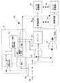
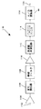
図6は、この発明の別の実施例に基づく波形測定システム400の例を示す。波形測定システム100は、光学スプリッタ600、光学変調器(ゲート)608および610、光/電気(O/E)変換器612および613、スプリッタ616、O/E変換器604、スプリッタ606、タイミング発生回路12(これはシリアルマーカー発生回路106、クロック復元回路108、および指令/ゲート信号発生回路110を含む)、変換回路120および121、およびアナログ/デジタル変換回路122及び123を含む。その波形測定システムは、光学分離器に結合された光アンプを含むことができる。光アンプは典型的に、システムにエネルギーを供給するエルビウム(希土類)のポンプレーザにドープされたファイバからなる。スプリッタ600は、基本的に電気カプラーに似ており、ツイストファイバまたは平面導波管である。光学変調器608および610は、送信機がデータ送信システムに用いられた時、その送信機での変調データ信号に似ている。これらは、典型的にリチウム ニオベイトの干渉計配列の変調器である。O/E変換器612は、フォトダイオードからなり、これにはある増幅器(通常、インピーダンス変換用の増幅器)が接続される。当業者なら、波形測定システム100を実施するために、他の構成の変調器、スプリッタ、O/E変換器および他の部品を使用できることが理解されよう。
FIG. 6 shows an example of a
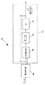
図7は、この発明の別の実施例に基づく波形測定システム100を例示する。波形測定システム100は、スプリッタ702、ゲート114および116、指令/ゲート信号発生回路700、スプリッタ118、変換回路120および121、およびアナログ/デジタル変換回路122および123を含む。イネーブル信号704は、指令/ゲート信号発生回路700に供給される。従って、指令/ゲート信号発生回路700により生じたエラーが存在する。他の実施例では、ゲート114および116は、旧来のオシロスコープ(周知なようにこれはトリガー回路およびプログラム可能な時間遅延を含む)の時間ベースによりイネーブルされ得る。
FIG. 7 illustrates a
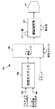
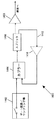
図8は、この発明に基づくエラー測定回路800の実施例を示す。図8の実施例は、エラーを補償するための波長多重化技術を示す。当業者には理解されるように、電気的な回路や時間ベースの回路を含む他の回路を使用できる。エラー測定回路800は、光学スプリッタ802、指令回路812、連続波(CW)レーザ804、マルチプレクサ806、光学変調器808、光学復調器810、およびO/E変換器814を含む。波長λ1の入力信号820は、波長λ2を有する基準レーザ信号822に結合される。光学変調器808は、タイミング発生回路812によりイネーブルにされる。光学復調器810は、波長λ1を有するサンプル化信号826から波長λ2を有する基準信号824を分離する。O/E変換器814および828は、サンプル化信号816および基準信号818を周波数サンプリングバンク(FSB)832および834に供給する。その周波数サンプリングバンク832および834は不図示のマイクロプロセッサまたは集積回路に結合され、バンク832、834で生成された情報は、ゲート808によるサンプル化信号816に導入された歪を修正するために用いられる。当業者なら理解されるように、エラー測定回路800は、光学要素に替えて電的な要素または両者の結合で実施できる。
FIG. 8 shows an embodiment of an
信号解析のための方法および装置では、入力信号のビットクロックを復元し、それを測定時間ベースとして用いることは有益になる。それにより、信号解析測定装置からビットクロックのエラーを除去できる。信号に関係するジッターを測定するためにも有利になる。図4は、この発明に基づくビットクロック復元回路の1実施例を示す。図11は、この発明に基づくジッター測定回路1100の実施例を示す。ジッター測定回路1100は、図1の実施例中のスプリッタ104に結合できる。それとは別に、ジッター測定回路1100は、他のいずれかのシリアル通信信号からであってもよい。ジッター測定回路1100は、制限用アンプ1104、変化検出器1106、狭帯域パスフィルタ1108、制限用アンプ1110、周波数弁別回路1112、アンチエイリアシング・フィルタ1114およびアナログ/デジタル変換器1116を含む。入力するシリアルデータ信号1102は制限用アンプ1104に供給される。この実施例では、狭帯域パスフィルタ1108は、ほぼ10GHz以下の信号を、10GB/sのデータ速度で制限用アンプ1110に通過させる。制限用アンプ1104および1110は、信号の振幅変化を最小にする。周波数弁別回路1112は、制限用アンプ1110により与えられた瞬時の周波数の関数となる出力電圧を与える。信号1124は、低周波および/又は中間周波のジッターを解析するためにワークステーション上の解析プログラムの制御下で動作するワークステーションに供給される。低周波のジッターは典型的におよそ10Hzから1MHzである。中間周波のジッターは典型的におよそ周波数の5から10%である。ジッターを解析する方法および装置は、ここで参考のために示した米国特許No. 6,356,850 の“ジッター解析のための方法および装置”に開示されている。当業者には周知なように、信号1124は、DSP機能、自動修正、FFT、範囲、ピークからピーク、平均、標準偏差、静止情報、ヒストグラムおよび他の解析を実行するために用いることができる。
In a method and apparatus for signal analysis, it is beneficial to recover the bit clock of the input signal and use it as a measurement time base. Thereby, a bit clock error can be removed from the signal analysis measurement apparatus. It is also advantageous for measuring jitter related to the signal. FIG. 4 shows an embodiment of a bit clock recovery circuit according to the present invention. FIG. 11 shows an embodiment of a
図12は、この発明に基づくジッター測定回路1200の実施例を示す。このジッター測定回路1200は、制限用アンプ1204、変化検出器1206、狭帯域パスフィルタ1208、制限用アンプ1210、PLL(位相検出器1218、ループフィルタ1226およびVCO 1220を含む)、アンチエイリアシング・フィルタ1228、およびアナログ/デジタル変換器1230を含む。入力するシリアルデータ信号1202は制限用アンプ1204に供給される。この実施例では、狭帯域パスフィルタ1208は、ほぼ10GHzの信号を、10GB/sの速度で制限用アンプ1210に通過させる。信号1132は、ワークステーション(これは内蔵の解析プログラムの制御下で動作する)に供給され、低周波および/またはゆらぎを解析する。低周波のジッターは、典型的に10Hzから1MHzである。信号1222はVCO 1220からビットクロックを与える。図1による実施例では、ジッター測定回路1200は、クロック復元回路108の実施例であり、入力信号102のジッター解析を可能にする。復元されたビットクロックは、周波数測定回路1221に提供され、これは、時間測定値のスケールを与え、そして/又は、復元されたビットクロックが満足できるかを検証する。典型的な周波数測定回路1221は、周波数カウンタおよび正確な時間ベースを含む。
FIG. 12 shows an embodiment of a
図13は、この発明に基づくジッター測定回路の別の実施例を示す。このジッター測定回路1300は、制限用アンプ1304、変化検出器1306、広帯域パスフィルタ1308、ミキサー1334、クロック1338、狭帯域パスフィルタ1336、制限用アンプ1310、PLL(位相検出器1318、ループフィルタ1326、およびVCO 1320を含む)、アンチエイリアシング・フィルタ1328、アナログ/デジタル変換器1330、ミキサー1340および広帯域パスフィルタ1342を含む。入力するシリアルデータ1302は、制限用アンプ1304に提供される。広帯域パスフィルタ1308は典型的に、10GHz以上の信号をミキサー1334に通過させる。ミキサー1334は、9.5GHzで動作しているクロック1338により駆動され、信号を500MHzに低下させ、PLLに与える。ミキサー1340は、信号を10GHzに上げ、そして、広帯域パスフィルタ1342をイネーブルにしてビットクロック信号1322を与える。図1の実施例では、ジッター測定回路1300は、クロック復元回路108の実施例である。信号1332は、低周波および/または中間周波のジッターを解析するために、分析プログラムの制御下で動作するワークステーションに与えられる。
FIG. 13 shows another embodiment of the jitter measurement circuit according to the present invention. This
いくつかの実施例では、ゲート制御機能の幅は、測定能力を最適にするために調節できる。人が振幅しきい値のクロス点を探しているような、あるケースでは、各測定を行うために多くの情報を必要としない。もっぱら波形の関心ある部分は、しきい値とクロスする部分である。この場合、測定手順は、適切な方法で進行できる。一般に、より広いゲート処理のウインドウは、しきい値の変化エリア内で波形全体の観察を得るために用いられることができる。一旦、変化が見つかると、ゲート処理のウインドウは、測定のために要求されるより低い高調波の個数を減じて狭められる。もし、周波数分解チャンネルが周波数において機敏なら、より高い周波数成分を観察して機敏な帯域測定を可能にするために、より低い高調波チャンネルが“再割り当て”される。 In some embodiments, the width of the gate control function can be adjusted to optimize measurement capability. In some cases, such as when a person is looking for an amplitude threshold crossing point, a lot of information is not needed to make each measurement. The part of the waveform that is of interest is the part that crosses the threshold. In this case, the measurement procedure can proceed in an appropriate manner. In general, a wider gating window can be used to obtain an observation of the entire waveform within the threshold change area. Once a change is found, the gating window is narrowed by reducing the number of lower harmonics required for measurement. If the frequency resolving channel is agile in frequency, the lower harmonic channel is “reassigned” to observe higher frequency components and allow for agile band measurement.
他の実施例では、二つ以上のゲート処理用のヘッドを一つの信号経路に用いることができる。これは“ストラドル(straddle)”ゲート処理と呼ばれる。一つの信号経路に二つのゲート処理用ヘッドを用いた形態では、関心対象の特徴に適切に到達できるように、二つのヘッドのゲート制御時間をそれぞれ移動できる。ストラドル測定の一つのスキームは、第1の時間ポイントで、そして再度、第2の時間ポイントで反復性信号を測定することを含み、意図した目的は、反復性信号がしきい値とクロスする時間ポイントを決定することである。二つの測定値は、しきい値をまたぐべきである。もし二つの測定値がしきい値をまたがらない場合、波形のその後の反復を待ち、そのポイントで、二つの測定が時間的に前方または後方に移動される。このプロセスは、測定値がしきい値をまたぐまで継続される。測定値の双方がしきい値の許容内に無いなら、信号のその後の反復を待機する。信号のその後の反復に到達すると、第1および第2の測定は、信号がしきい値とクロスする時間のポイントに向けてステップ移動される。このプロセスは、測定値の一つが目的とされるしきい値の許容内になるまで繰返される。 In other embodiments, two or more gate processing heads can be used in one signal path. This is called “straddle” gating. In the configuration using two gate processing heads in one signal path, the gate control times of the two heads can be moved so as to appropriately reach the feature of interest. One scheme of straddle measurement involves measuring a repetitive signal at a first time point and again at a second time point, the intended purpose being the time at which the repetitive signal crosses a threshold value. The point is to decide. The two measurements should cross the threshold. If the two measurements do not cross the threshold, then wait for a subsequent iteration of the waveform, at which point the two measurements are moved forward or backward in time. This process continues until the measured value crosses the threshold. If both of the measured values are not within the threshold tolerance, wait for a subsequent iteration of the signal. When a subsequent iteration of the signal is reached, the first and second measurements are stepped towards the point in time where the signal crosses the threshold. This process is repeated until one of the measured values is within the intended threshold tolerance.
上述したスキームは、ユーザーによりしきい値が選択できるようにすることで改善される。従って、第1および第2の測定がしきい値クロス点への移動回数も同様に選択されてもよい。 The scheme described above is improved by allowing the user to select a threshold value. Accordingly, the number of movements of the first and second measurements to the threshold crossing point may be selected in the same manner.
ストラドルのゲート制御は、関心のポイントが小さい一時的な位置に制限できる時、すべての状況において波形を一様にサンプリングする必要性を排除できる。このような均一でないゲート制御は、波形全体の観察が必要な時に有用であるが、関心あるエリアが波形の特性に制限される時には極めて有効的でない。 Straddle gating can eliminate the need to sample the waveform uniformly in all situations when the point of interest can be limited to a small temporary position. Such non-uniform gating is useful when it is necessary to observe the entire waveform, but is not very effective when the area of interest is limited to the characteristics of the waveform.
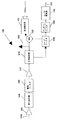
図14は、この発明に基づく光再伝達システム1400の実施例を示す。この光再伝達システム1400は、ゲート制御された波形を反復して測定システムへ提供する結果を達成する。これにより、例えば、ゲート処理の結果により、誤ったビットが測定から隔離されたなら、この光再伝達システム1400は、その誤ったビットを測定システム(図14では不図示)に対して正確に何回も“再生”する。その測定システムは、その後でその誤ったビットを正確に測定するために、そのビットを複数回の“再生”できる利点を有する。例えば、この測定システムは、測定のエラー内容を減じるために“再生された”各波形を測定でき、多数の測定を平均する。これとは別に、測定システムは、波形の各繰り返しに対し、その波形を異なる位置でサンプリングして、測定システムにより達成されるサンプリング密度を強めることができる。
FIG. 14 shows an embodiment of an
この再伝達システム1400は、そのフロント端にゲート回路1402を含む。このゲート回路1402は、再伝達のための光波形のセグメントと、その後の測定値とを分離する。そのゲート回路1402の出力は、光学カプラー1404に結合され、そこで第1および第2の入力を有する。そのゲート回路1402は、カプラー1404の第1の入力部に結合される。そのカプラーは、第1および第2の入力部から入力された信号を結合し、その結合を出力ラインに出力する。その出力ラインは、スプリッタ1406に接続され、これは第1および第2の出力ラインを有する。そのスプリッタ1406は、その入力部での信号の一部を、その第1の出力ラインに出力し、そして、前記信号の一部を第2の出力ラインに出力する(例えば第1の出力ラインに5%,第2の出力ラインに95%)。第1の出力ラインは、もし必要ならばアンプ1408を通じて測定システム(不図示)に接続される。第2の出力ラインは、ファイバーループ1412を通じてカプラー1404の第2の入力部に接続される。追加的なアンプ1410がファイバーループ1412に挿入されてもよい。そのカプラー1404、スプリッタ1046、ファイバーループ1412およびアンプ1410は、ループ(ゲート処理された波形が伝達)を形成するために協働し、ゲート処理された波形の一部は分離され、伝達毎に測定システムに導かれる。
The
エイリアシング(サンプリングにより発生する偽信号)を防止するために、ファイバーループ1412ファイバー長を持つべきであり、これにより、ファイバーループの一端から他端に伝播する光波が、ゲート回路1402により採用されたゲート処理期間よりも大きい時間の期間で衰えるようにする。追加的に、アンプ1410は、測定システムにとって有用であると立証するために、波形が分かる十分な回数で伝達させることを可能にするに十分となるように、選択された利得レベルを用いなくてはならない。他方、アンプ1410は、ファイバーループ1412が飽和しないように、選択された十分に低い利得レベルを用いなくてはならない。そのような利得レベルは、“適した利得”として述べる。
To prevent aliasing (false signal generated by sampling), the fiber loop should have a 1412 fiber length, so that the light wave propagating from one end of the fiber loop to the other is gated by the
上述した実施例は、多くの方法で結合されてもよく、また、自身の権限によって発明として、独立して分離されてもよい。例えば、図1〜14の各図に示された実施例は、発明として独立してもよい。これとは別に、図1〜14に記載された実施例を同時に機能させるために結合してもよい。限定されない例として、実施例が次のように結合されてもよい。(1)異常な波形セグメントがゲート処理のために分離され、セグメントがサンプリングされるように、異常検出器は、遅延要素および測定ユニットに結合されてもよく、これは更に、セグメントのサンプリング器に結合されてもよい。(2)異常ビットが測定できるように、ビットクロック復元回路は、測定ユニットに測定イネーブル信号を送出する、異常検出器をクロック制御するために用いられてもよく、その測定ユニットもビット復元回路によりクロック制御されてもよい。(3)参照した図8のアーキテクチャーは、セグメントのサンプリング器と結合して、非多重化のゲート制御信号がそれによって測定されてもよい。(4)参照した図8のアーキテクチャーは、内部のゲートが異常波形を分離するために、異常検出器と結合されてもよい。(5)図14の再伝達器は、ビットクロック復元回路と結合されてもよく、それにより、再伝達器内のゲートが復元されたビットクロック、または、それから引き出された信号により駆動される。(6)図14の再伝達器は、異常検出器と結合して、異常波形のセグメントが分離され、再伝達されるようにしてもよい。(7)図14の再伝達器は、ストラドル測定スキームを採用した測定ユニットと結合して、しきい値のクロスが決定されてもよい。(8)図14の再伝達器は、ストラドル測定スキームを採用した測定ユニットと結合し、この測定ユニットは更に異常検出器と結合して、分離された再伝達された波形セグメントは異常であり、しきい値に含まれるクロスが決定されるようにしてもよい。(9)図14の再伝達器は、ストラドル測定スキームを採用した測定ユニットと結合し、この測定ユニットは更にビットクロック復元回路に結合され、再伝達器内のゲートがビットクロックにより駆動されてもよい。 The embodiments described above may be combined in a number of ways and may be independently separated as an invention by their own authority. For example, the embodiments shown in FIGS. 1 to 14 may be independent as inventions. Alternatively, the embodiments described in FIGS. 1-14 may be combined to function simultaneously. As a non-limiting example, the embodiments may be combined as follows. (1) The anomaly detector may be coupled to a delay element and a measurement unit so that the anomalous waveform segments are separated for gating and the segments are sampled, which is further connected to the segment sampler. May be combined. (2) The bit clock recovery circuit may be used to clock an abnormality detector that sends a measurement enable signal to the measurement unit so that an abnormal bit can be measured. It may be clocked. (3) The referenced architecture of FIG. 8 may be combined with a segment sampler, whereby a demultiplexed gate control signal may be measured. (4) The referenced architecture of FIG. 8 may be combined with an anomaly detector so that the internal gate separates the anomalous waveform. (5) The retransmitter of FIG. 14 may be combined with a bit clock recovery circuit so that the gate in the retransmitter is driven by the recovered bit clock or a signal derived therefrom. (6) The retransmitter of FIG. 14 may be combined with an anomaly detector so that abnormal waveform segments are separated and retransmitted. (7) The transmitter of FIG. 14 may be combined with a measurement unit employing a straddle measurement scheme to determine a threshold crossing. (8) The retransmitter of FIG. 14 is coupled to a measurement unit employing a straddle measurement scheme, which is further coupled to an anomaly detector, and the separated retransmitted waveform segment is abnormal, A cross included in the threshold may be determined. (9) The transmitter of FIG. 14 is coupled to a measurement unit employing a straddle measurement scheme, which is further coupled to a bit clock recovery circuit, even if the gate in the transmitter is driven by a bit clock. Good.
上述した種々の実施例は、図示のみの方法で与えられており、この発明を限定するものではない。当業者なら、提示した実施例およびここで述べ、かつ図示した明細書なしで、そしてこの発明の趣旨および範囲から逸脱することなく、この発明になる種々の実施例および変形を実現できるであろう。 The various embodiments described above are given by way of illustration only and are not intended to limit the invention. Those skilled in the art will be able to implement the various embodiments and variations that come within the scope of the invention without the specification presented and the specification described and illustrated herein, and without departing from the spirit and scope of the invention. .
この発明は、種々の変形、変更した形態への適用は容易であり、それの特定形態が図面の例を用いて開示され、詳細に述べられている。しかしながら、この発明は述べられた特定の実施例に限定されないことが理解されよう。一方、この発明は、この発明の範囲内のすべての変形、等価品、変更をカバーする。 The present invention can be easily applied to various modifications and changes, and specific forms thereof are disclosed and described in detail using examples of the drawings. It will be understood, however, that the invention is not limited to the specific embodiments described. On the other hand, the present invention covers all modifications, equivalents, and modifications within the scope of the present invention.
12 タイミング発生回路
100 波形測定システム
104 スプリッタ
106 シリアルデータマーカー発生回路
108 クロック復元回路
109 周波数測定回路
110 指令/ゲート信号発生回路
112 アナログ・デジタル変換回路
114 ゲート
120 変換回路
12
Claims (62)
波形を受信し、
波形をゲート処理し、これにより、第1の時間ポイントの以前では実質的に静止し、第1の時間ポイントと第2の時間ポイントとの間では前記波形に実質的に等しく、そして、第2の時間ポイント移行で実質的に静止している、ゲート処理された波形を生成し、そして、
ゲート処理された波形を多数の周波数情報抽出器に提供することを含み、
各周波数情報抽出器は、各周波数情報抽出器における固有の周波数に対し、ゲート処理された波形の振幅または位相内容の少なくとも一つに関する情報を生成し、その結果、そのゲート処理された波形が、多数の周波数情報抽出器から生成された情報で表される、方法。 A method of measuring segments of a waveform,
Receive the waveform,
Gating the waveform so that it is substantially stationary before the first time point, substantially equal to the waveform between the first time point and the second time point, and the second Generate a gated waveform that is substantially stationary at a time point transition of
Providing a gated waveform to a number of frequency information extractors;
Each frequency information extractor generates information about at least one of the amplitude or phase content of the gated waveform for the unique frequency in each frequency information extractor, so that the gated waveform is A method represented by information generated from a number of frequency information extractors.
波形を受信し、
第1の経路および第2の経路に沿って波形を伝え、第1の経路は遅延エレメントに結合され、そして、第2の経路は波形異常検出器に結合され、波形異常検出器は、異常を含んだ波形を検出した時に測定イネーブル信号を発生し、
遅延エレメントからの波形を波形測定デバイスに伝え、そして
波形異常検出器により発生された測定イネーブル信号で波形測定デバイスを能動化させ、これにより、遅延エレメントから導かれた波形内に存在する異常の到達と実質的に同時に、測定イネーブル信号が波形測定デバイスに到達するようになっている方法。 It is a method to measure waveform abnormality,
Receive the waveform,
A waveform is conveyed along the first path and the second path, the first path is coupled to the delay element, and the second path is coupled to the waveform abnormality detector, and the waveform abnormality detector Generates a measurement enable signal when a contained waveform is detected,
Transmits the waveform from the delay element to the waveform measurement device and activates the waveform measurement device with the measurement enable signal generated by the waveform anomaly detector so that an anomaly present in the waveform derived from the delay element is reached Substantially simultaneously with the measurement enable signal reaching the waveform measurement device.
遅延エレメントから波形を受信し、
波形をゲート処理し、これにより、トリガー信号の受信前では実質的に静止し、トリガー信号の受信と第2の時間ポイントとの間では前記波形に実質的に等しく、そして、第2の時間ポイント移行で実質的に静止している、ゲート処理された波形を生成し、そして、
ゲート処理された波形を多数の周波数情報抽出器に提供することを含み、
各周波数情報抽出器は、各周波数情報抽出器における固有の周波数に対し、ゲート処理された波形の振幅または位相内容に関する情報を生成し、その結果、そのゲート処理された波形が、多数の周波数情報抽出器から生成された情報により表される、方法。 Waveform measurement device
Receive the waveform from the delay element,
Gating the waveform so that it is substantially stationary before receiving the trigger signal, substantially equal to the waveform between receiving the trigger signal and the second time point, and a second time point Generate a gated waveform that is substantially stationary at the transition, and
Providing a gated waveform to a number of frequency information extractors;
Each frequency information extractor generates information about the amplitude or phase content of the gated waveform for the unique frequency in each frequency information extractor, so that the gated waveform contains a large amount of frequency information. A method represented by information generated from an extractor.
波形を受信し、
波形内にエンコードされたクロック信号を復元し、
復元されたクロック信号に基づき、第1の基準クロック信号を発生し、そして
第1の基準クロック信号に関連する固定された周波数内の時間ポイントにて、受信された波形の振幅を測定することを備える方法。 A method for measuring a waveform having an encoded clock signal,
Receive the waveform,
Restore the clock signal encoded in the waveform,
Based on the recovered clock signal, generating a first reference clock signal and measuring the amplitude of the received waveform at a time point within a fixed frequency associated with the first reference clock signal. How to prepare.
第1の基準クロックは周波数を有し、そして、
第1の基準クロック信号の周波数は復元されたクロック信号の周波数の倍数である請求項13に記載の方法。 The recovered clock signal has a frequency,
The first reference clock has a frequency, and
The method of claim 13, wherein the frequency of the first reference clock signal is a multiple of the frequency of the recovered clock signal.
第2のサンプリングクロック信号に関連する固定された周波数における時間ポイントにて第2の波形を測定することを更に備える請求項13記載の方法。 14. The method of claim 13, further comprising: generating a second reference signal based on the received clock signal; and measuring the second waveform at a time point at a fixed frequency associated with the second sampling clock signal. Method.
複製した波形を遅延させ、
第1の基準クロック信号に関連した固定の周波数における時間ポイントにて受信した波形を測定することで、受信した波形内の異常を検出し、そして
異常が検出された時、第1の基準クロック信号に関連する固定の周波数における時間ポイントで遅延した複製波形を測定することを更に備える請求項13記載の方法。 Duplicate the received waveform,
Delay the duplicated waveform,
By measuring the received waveform at a time point at a fixed frequency associated with the first reference clock signal, an abnormality in the received waveform is detected, and when an abnormality is detected, the first reference clock signal The method of claim 13, further comprising measuring a replicated waveform delayed at a time point at a fixed frequency associated with.
第1の周波数で搬送された波形を受信し、
第2の周波数を有する基準信号を発生し、
受信した波形および基準波形を周波数空間で多重化し、
多重化信号をゲート処理し、それにより、第1の時間ポイント以前で実質的に静止し、第1の時間ポイントと第2の時間ポイントとの間では前記多重化信号に実質的に等しく、そして、第2の時間ポイント以降では実質的に静止しているゲート処理された多重化波形を生じ、
ゲート処理された多重化波形を復調し、それにより、第1の周波数で搬送されるゲート処理された波形およびゲート処理された基準波形を生成し、そして
第1の周波数で搬送されるゲート処理された波形に導入されたゲート処理による歪を、ゲート処理された基準波形に基づき決定することを備える方法。 A method for identifying distortion introduced into a waveform by gating the waveform;
Receiving a waveform carried at a first frequency;
Generating a reference signal having a second frequency;
Multiplex received waveform and reference waveform in frequency space,
Gating the multiplexed signal so that it is substantially stationary before the first time point, substantially equal to the multiplexed signal between the first time point and the second time point; and Produces a gated multiplexed waveform that is substantially stationary after the second time point,
Demodulate the gated multiplexed waveform, thereby generating a gated waveform and a gated reference waveform carried at the first frequency, and a gated waveform carried at the first frequency Determining the distortion due to gating introduced into the waveform based on the gated reference waveform.
光波をゲート処理し、それにより、第1の時間ポイント以前で実質的に静止し、第1の時間ポイントと第2の時間ポイントとの間では、実質的に前記光波に等しく、そして、第2の時間ポイント以降で実質的に静止しているゲート処理された光波を生じ、
ゲート処理された光波を光学カプラーの第1の入力部に供給し、この光学カプラーは追加的に第2の入力部および出力部を有し、その光学カプラーはその入力部に与えられた信号を結合し、そしてその結合したものをその出力部に出力し、光学カプラーのその出力は、光学スプリッタに結合され、そのスプリッタは、その入力部の第1の部分を第1の出力部に出力し、その入力部の第2の部分を第2の出力部に出力し、スプリッタの第2の出力部はファイバーループを通じて光学カプラーの第2の入力部に結合され、光学スプリッタの第1の出力部は測定システムに結合され、それにより、ゲート処理された波形が反復して測定システムに与えられる方法。 Receiving light waves,
Gating the light wave so that it is substantially stationary before the first time point, substantially equal to the light wave between the first time point and the second time point, and second Produces a gated light wave that is substantially stationary after the time point of
A gated light wave is supplied to a first input of an optical coupler, the optical coupler additionally having a second input and an output, the optical coupler receiving a signal applied to the input And outputs the combination to the output, the output of the optical coupler is coupled to an optical splitter, and the splitter outputs the first part of the input to the first output. A second portion of the input is output to the second output, the second output of the splitter being coupled through a fiber loop to the second input of the optical coupler, and the first output of the optical splitter Is coupled to a measurement system, whereby a gated waveform is repeatedly applied to the measurement system.
復元されたクロック信号から発生された信号によって、光波をゲート処理することを更に備える請求項23記載の方法。 The light wave has a clock signal encoded therein, and the method further comprises receiving the clock signal from the light wave and gating the light wave with the signal generated from the recovered clock signal. Item 24. The method according to Item 23.
第1の時間ポイントおよび第2の時間ポイントで反復性信号をサンプリングすることを備え、
そして、二つのサンプリング値のいずれもがしきい値の許容値内に無いならば、
信号のその後の反復のために待機し、
信号がしきい値にクロスする時間ポイントに向けて、二つの測定点をステップ移動させ、そして
サンプリング値の一つがしきい値の許容値内に達するまで、二つのステップ移動を繰返すことを行う方法。 A method for automatically determining the time point at which a repetitive signal crosses a threshold;
Sampling a repetitive signal at a first time point and a second time point;
And if neither of the two sampling values are within the threshold tolerance,
Wait for subsequent iterations of the signal,
A method of stepping two measurement points towards the time point at which the signal crosses the threshold, and repeating the two-step movement until one of the sampling values falls within the threshold tolerance. .
光波を受信し、
その光波をゲート処理し、それにより、第1の時間ポイント以前で実質的に静止し、第1の時間ポイントと第2の時間ポイントとの間では前記光波に実質的に等しく、そして、第2の時間ポイント以降では実質的に静止した、ゲート処理された光波を生じ、
ゲート処理された光波を光学カプラーの第1の入力部に供給し、前記光学カプラーは追加的に第2の入力部と出力部を有し、前記光学カプラーは、その入力部に与えられた信号を結合し、そして、その出力部にその結合信号を出力し、光学カプラーの出力部は光学スプリッタに結合され、そのスプリッタは、その入力の第1の部分を第1の出力部に出力し、そして、前記入力部の第2の部分を第2の出力部に出力し、スプリッタの第2の出力部はファイバーループを通じて光学カプラーの第2の入力部に結合され、光学カプラーの第1の出力部は、請求項28で述べたように動作する測定システムに結合され、これにより、請求項28で述べたように動作する測定システムへ反復して供給されるゲート処理された波形を生じる請求項28記載の方法。 The repetitive signal is generated by the following steps:
Receiving light waves,
Gating the light wave so that it is substantially stationary before the first time point, substantially equal to the light wave between the first time point and the second time point, and second After this time point, it produces a substantially stationary, gated light wave,
A gated light wave is supplied to a first input of an optical coupler, the optical coupler additionally having a second input and an output, the optical coupler being a signal applied to the input And the output of the optical coupler is coupled to an optical splitter, which outputs a first portion of its input to a first output; The second portion of the input section is then output to a second output section, and the second output section of the splitter is coupled to the second input section of the optical coupler through a fiber loop, and the first output of the optical coupler is output. The portion is coupled to a measurement system operating as set forth in claim 28, thereby producing a gated waveform that is repeatedly supplied to the measurement system operating as set forth in claim 28. 28 description Method.
前記光波からクロック信号を受信し、
受信したクロック信号から発生された信号で前記光波をゲート処理することを更に備える請求項30記載の方法。 The light wave has a clock signal encoded therein, and the method includes:
Receiving a clock signal from the light wave;
31. The method of claim 30, further comprising gating the light wave with a signal generated from a received clock signal.
波形をゲート処理し、それにより、第1の時間ポイント以前で実質的に静止し、第1の時間ポイントと第2の時間ポイントとの間では前記波形に実質的に等しく、そして第2の時間ポイント以降で静止しているゲート処理された波形を生じるゲート処理回路と、
前記ゲート処理回路に結合される多数の周波数情報抽出器であり、それぞれがゲート処理された波形を入力として受信し、それぞれが、それぞれに対する固有の周波数に対し、ゲート処理された波形の振幅および位相内容に関する情報を生成し、ゲート処理された波形はその結果、多数の周波数情報抽出器から生成された情報によって表される、多数の周波数情報抽出器とを備えるシステム。 A system for measuring segments of a waveform,
Gating the waveform so that it is substantially stationary before the first time point, substantially equal to the waveform between the first time point and the second time point, and a second time A gate processing circuit that produces a gated waveform that is stationary after the point; and
A number of frequency information extractors coupled to the gate processing circuit, each receiving as input a gated waveform, each of which has a gated waveform amplitude and phase for a specific frequency for each. A system comprising a number of frequency information extractors that generate information about the content and the gated waveform is thereby represented by information generated from a number of frequency information extractors.
ゲート処理された波形を実質的に示す時間関数を、多数の周波数情報抽出器から生成された情報に基づき、決定できるようにプログラムされているプロセッサを更に備える請求項33記載のシステム。 A processor coupled to multiple frequency information extractors, receiving information from multiple frequency information extractors through an input port,
34. The system of claim 33, further comprising a processor programmed to determine a time function substantially indicative of the gated waveform based on information generated from a number of frequency information extractors.
波形を受信し、そしてその波形を第1の経路および第2の経路に導くスプリッタと、
第1の経路に結合された遅延エレメントと、
第2の経路に接続され、異常を含む信号が検出されると、測定イネーブル信号を出力する波形異常検出器と、
遅延要素に結合された波形測定デバイスとを備え、
波形測定デバイスは、波形異常検出器で発生された測定イネーブル信号が能動化させ、その結果、遅延エレメントから導かれた波形内に存在する異常の到達と実質的に同時に、測定イネーブル信号が波形測定デバイスに到達するシステム。 A system for measuring waveform anomalies,
A splitter that receives the waveform and directs the waveform to a first path and a second path;
A delay element coupled to the first path;
A waveform abnormality detector that is connected to the second path and outputs a measurement enable signal when a signal including an abnormality is detected;
A waveform measuring device coupled to the delay element,
The waveform measurement device activates the measurement enable signal generated by the waveform anomaly detector so that the measurement enable signal is waveform measured substantially simultaneously with the arrival of an anomaly present in the waveform derived from the delay element. The system that reaches the device.
測定イネーブル信号の受信により、遅延エレメントからの波形をゲート処理し、それにより、測定イネーブル信号の受信以前で実質的に静止し、測定イネーブル信号の受信と第2の時間ポイントとの間では前記波形に実質的に等しく、そして、第2の時間ポイント以降で実質的に静止している、ゲート処理された波形を生じるゲート回路と、
前記ゲート処理回路に結合される多数の周波数情報抽出器であり、それぞれがゲート処理された波形を入力として受信し、それぞれが、それぞれに対する固有の周波数に対し、ゲート処理された波形の振幅および位相内容に関する情報を生成し、ゲート処理された波形はその結果、多数の周波数情報抽出器から生成された情報によって表される、多数の周波数情報抽出器とを備えるシステム。 Waveform measurement device
Upon receipt of the measurement enable signal, the waveform from the delay element is gated, thereby substantially quiescing before reception of the measurement enable signal, and between the reception of the measurement enable signal and the second time point, the waveform. A gating circuit that produces a gated waveform that is substantially equal to and substantially stationary after the second time point;
A number of frequency information extractors coupled to the gate processing circuit, each receiving as input a gated waveform, each of which has a gated waveform amplitude and phase for a specific frequency for each. A system comprising a number of frequency information extractors that generate information about the content and the gated waveform is thereby represented by information generated from a number of frequency information extractors.
波形内のエンコードされたクロック信号を復元する復元回路と、
復元回路に結合され、受信したクロック信号に基づき第1の基準クロック信号を発生するクロック発生回路と、
第1の基準クロック信号に関連する固定された周波数内の時間ポイントにて、受信した波形の振幅を測定する波形測定デバイスとを備えるシステム。 A system for measuring a waveform having an encoded clock signal;
A recovery circuit for recovering the encoded clock signal in the waveform;
A clock generation circuit coupled to the restoration circuit and generating a first reference clock signal based on the received clock signal;
And a waveform measuring device that measures the amplitude of the received waveform at a time point in a fixed frequency associated with the first reference clock signal.
第1の経路に結合される遅延エレメントと、そして
第2の経路に接続された波形異常検出器であり、異常が含まれる波形を検出すると、測定イネーブル信号を発生し、第1の基準クロック信号に関連する固定された周波数内の時間ポイントにて、受信した波形を測定することにより、受信した波形内の異常を検出する波形異常検出器とを更に備え、
波形測定デバイスは遅延エレメントに結合され、波形測定デバイスは、波形異常検出器で発生された測定イネーブル信号が能動化させ、その結果、遅延エレメントから導かれた波形内に存在する異常の到達と実質的に同時に、測定イネーブル信号が波形測定デバイスに到達するシステム。 A splitter that receives the waveform and directs it to a first path and a second path;
A delay element coupled to the first path; and a waveform anomaly detector connected to the second path, wherein when a waveform including an anomaly is detected, a measurement enable signal is generated and a first reference clock signal A waveform anomaly detector for detecting an anomaly in the received waveform by measuring the received waveform at a time point within a fixed frequency associated with
The waveform measurement device is coupled to the delay element, and the waveform measurement device is activated by the measurement enable signal generated by the waveform anomaly detector so that the presence of an anomaly present in the waveform derived from the delay element is substantially detected. At the same time, a system in which the measurement enable signal reaches the waveform measurement device.
第2の周波数を有する基準信号を発生するレーザと、
第1の周波数で搬送された波形と基準信号を多重化する周波数空間のマルチプレクサと、
マルチプレクサに結合されたゲート回路であり、多重化された信号をゲート処理し、それにより、第1の時間ポイント以前では実質的に静止し、第1のポイントと第2のポイントとの間では前記多重化された信号に実質的に等しく、そして、第2の時間ポイント以降では実質的に静止している、ゲート処理され、多重化された波形を生じるゲート回路と、
ゲート回路に結合されたデマルチプレクシング回路であり、ゲート処理され、多重化された波形をデマルチプレクシングし、それにより、第1の基準周波数で搬送されたゲート処理された波形と、ゲート処理され他基準信号を生じるデマルチプレクシング回路と、
デマルチプレクシング回路に結合された測定ユニットであり、ゲート処理された基準信号および第1の周波数で搬送されるゲート処理された波形に関する情報を取得してデジタル化する、測定ユニットと、および
測定ユニットに結合されたプロセッサであり、第1の周波数で搬送されるゲート処理された波形に導入された歪を、ゲート処理された基準信号に基づき、ゲート処理することを決定するようにプログラム化されたプロセッサとを備えるシステム。 A system for identifying distortion introduced into a waveform by gating the waveform,
A laser that generates a reference signal having a second frequency;
A frequency space multiplexer for multiplexing the waveform carried at the first frequency and the reference signal;
A gate circuit coupled to a multiplexer for gating the multiplexed signal so that it is substantially stationary before the first time point and between the first point and the second point; A gating circuit that is substantially equal to the multiplexed signal and that is substantially stationary after the second time point to produce a gated multiplexed waveform;
A demultiplexing circuit coupled to a gating circuit, demultiplexing a gated and multiplexed waveform, thereby gated with a gated waveform carried at a first reference frequency A demultiplexing circuit for generating other reference signals;
A measurement unit, coupled to a demultiplexing circuit, for acquiring and digitizing information about a gated reference signal and a gated waveform carried at a first frequency, and a measurement unit Is programmed to determine that the distortion introduced into the gated waveform carried at the first frequency is to be gated based on the gated reference signal. A system comprising a processor.
光波をゲート処理するゲート回路であり、その結果、第1の時間ポイント以前で実質的に静止し、第1の時間ポイントおよび第2の時間ポイントとの間で実質的に前記光波に等しく、そして、第2の時間以降で実質的に静止している、ゲート処理された光波を生じるゲート回路と、
第1および第2の入力部と一つの出力部を有する光学カプラーであり、第1の入力部はゲート回路に結合され、これにより、ゲート処理された光波を受信し、第1および第2の入力部に与えられた信号を結合し、その結合したものをその出力部に出力する光学カプラーと、
光学カプラーの出力部に結合される光学スプリッタであり、その入力の第1の部分を第1の出力部に、その入力の第2の部分を第2の出力部に出力し、スプリッタの第2の出力部はファイバーループを通じて光学カプラーの第2の入力部に結合される光学スプリッタと、および
光学スプリッタの出力部に結合され、それにより、ゲート処理された波形を反復して受信する測定システムとを備えるシステム。 A system for repeatedly supplying a segment of a waveform to a measurement system;
A gating circuit for gating the light wave, so that it is substantially stationary before the first time point, substantially equal to the light wave between the first time point and the second time point, and A gate circuit that produces a gated light wave that is substantially stationary after the second time;
An optical coupler having a first and second input and an output, the first input being coupled to a gate circuit, thereby receiving the gated light wave, and the first and second An optical coupler for combining signals given to the input unit and outputting the combined signal to the output unit;
An optical splitter coupled to the output of the optical coupler, the first portion of the input being output to the first output, the second portion of the input being output to the second output, An output of the optical splitter coupled to the second input of the optical coupler through a fiber loop, and a measurement system coupled to the output of the optical splitter, thereby repeatedly receiving the gated waveform A system comprising:
光波にエンコードされたクロックを復元する復元回路と、
復元回路に接続され、受信したクロック信号に基づき、第1の基準クロック信号を発生するクロック発生回路とを備え、
ゲート回路は第1の基準クロック信号でクロック制御される請求項54記載のシステム。 The lightwave has a clock signal encoded therein, and the system further includes
A recovery circuit for recovering the clock encoded in the light wave;
A clock generation circuit connected to the restoration circuit and generating a first reference clock signal based on the received clock signal;
55. The system of claim 54, wherein the gate circuit is clocked with a first reference clock signal.
反復性信号を受信してサンプリングするサンプリングユニットと、
前記サンプリングユニットに結合され、そのサンプリングユニットにより行われるサンプリングのタイミングを制御するプロセッサとを備え、
このプロセッサは、
第1の時間ポイントおよび第2の時間ポイントで反復性信号をサンプリングし、
二つのサンプリング値のいずれもがしきい値の許容値内に無いならば、
信号のその後の反復を待機し、そして、信号がしきい値にクロスする時間ポイントに向けて、二つの測定点をステップ移動させ、そして、サンプリング値の一つがしきい値の許容値内に達するまで、二つのステップ移動を繰返すことを行う、波形測定デバイス。 A waveform measurement device that determines the time point at which a repetitive signal crosses a threshold,
A sampling unit for receiving and sampling repetitive signals;
A processor coupled to the sampling unit and controlling the timing of sampling performed by the sampling unit;
This processor
Sampling a repetitive signal at a first time point and a second time point;
If neither of the two sampling values is within the threshold tolerance,
Wait for subsequent iterations of the signal, and step two measurement points toward the time point where the signal crosses the threshold, and one of the sampled values reaches within the threshold tolerance A waveform measurement device that repeats two step movements until.
光波をゲート処理するゲート回路であり、これにより、第1の時間ポイント以前では実質的に静止し、第1の時間ポイントおよび第2の時間ポイントの間では前記光波に実質的に等しく、そして、第2の時間ポイント以降では実質的に静止している、ゲート処理された光波を生じるゲート回路と、
光学カプラーの出力部に結合される光学スプリッタであり、その入力の第1の部分を第1の出力部に、その入力の第2の部分を第2の出力部に出力し、スプリッタの第2の出力部はファイバーループを通じて光学カプラーの第2の入力部に結合される光学スプリッタと、および
波形測定デバイスのサンプリングユニットであり、光学スプリッタの出力部に結合され、それにより、ゲート処理された波形を反復して受信するサンプリングユニットとを備える請求項59記載の波形測定デバイス。 A repetitive signal is generated by the system, which
A gating circuit for gating the light wave, thereby substantially stationary before the first time point, substantially equal to the light wave between the first time point and the second time point, and A gate circuit that produces a gated light wave that is substantially stationary after the second time point;
An optical splitter coupled to the output of the optical coupler, the first portion of the input being output to the first output, the second portion of the input being output to the second output, The output of the optical splitter coupled to the second input of the optical coupler through the fiber loop, and the sampling unit of the waveform measuring device, coupled to the output of the optical splitter and thereby gated waveform 60. The waveform measuring device according to claim 59, comprising: a sampling unit that repeatedly receives the signal.
光波にエンコードされたクロックを復元する復元回路と、
復元回路に接続され、受信したクロック信号に基づき、第1の基準クロック信号を発生するクロック発生回路とを備え、
サンプリングユニットは第1の基準クロック信号でサンプリングを行うように命令される請求項59記載のシステム。
The light wave has a clock signal encoded therein, the light wave measuring device further comprising:
A recovery circuit for recovering the clock encoded in the light wave;
A clock generation circuit connected to the restoration circuit and generating a first reference clock signal based on the received clock signal;
60. The system of claim 59, wherein the sampling unit is instructed to sample with the first reference clock signal.
Applications Claiming Priority (2)
| Application Number | Priority Date | Filing Date | Title |
|---|---|---|---|
| US31410801P | 2001-08-22 | 2001-08-22 | |
| PCT/US2002/026996 WO2003044543A2 (en) | 2001-08-22 | 2002-08-22 | Method and apparatus for measuring a waveform |
Publications (2)
| Publication Number | Publication Date |
|---|---|
| JP2005509890A true JP2005509890A (en) | 2005-04-14 |
| JP2005509890A5 JP2005509890A5 (en) | 2006-01-05 |
Family
ID=23218587
Family Applications (1)
| Application Number | Title | Priority Date | Filing Date |
|---|---|---|---|
| JP2003546119A Pending JP2005509890A (en) | 2001-08-22 | 2002-08-22 | Method and apparatus for measuring waveforms |
Country Status (5)
| Country | Link |
|---|---|
| US (1) | US20030058970A1 (en) |
| EP (1) | EP1421395A2 (en) |
| JP (1) | JP2005509890A (en) |
| AU (1) | AU2002329836A1 (en) |
| WO (1) | WO2003044543A2 (en) |
Cited By (1)
| Publication number | Priority date | Publication date | Assignee | Title |
|---|---|---|---|---|
| WO2012021332A3 (en) * | 2010-08-13 | 2012-04-12 | Altera Corporation | Circuitry on an integrated circuit for performing or facilitating oscilloscope, jitter, and/or bit-error-rate tester operations |
Families Citing this family (16)
| Publication number | Priority date | Publication date | Assignee | Title |
|---|---|---|---|---|
| EP1367761B1 (en) * | 2002-05-29 | 2007-01-17 | Agilent Technologies, Inc. - a Delaware corporation - | Measurement of jitter in digital communications signals |
| US7627029B2 (en) | 2003-05-20 | 2009-12-01 | Rambus Inc. | Margin test methods and circuits |
| US7590175B2 (en) | 2003-05-20 | 2009-09-15 | Rambus Inc. | DFE margin test methods and circuits that decouple sample and feedback timing |
| DE10334963A1 (en) * | 2003-07-31 | 2005-03-03 | PARTEMA GmbH Parallele Technologie für Modul-Algorithmen | Signal analysis method e.g. for acoustic oscillations for control of synthesizer, using linear combinations of adjacent sampled values for solution of differential equations |
| US7778315B2 (en) * | 2004-04-14 | 2010-08-17 | Tektronix, Inc. | Measuring instantaneous signal dependent nonlinear distortion in response to varying frequency sinusoidal test signal |
| US7285946B2 (en) * | 2005-02-07 | 2007-10-23 | Lecroy Corporation | Pattern trigger in a coherent timebase |
| US20080072130A1 (en) * | 2006-05-31 | 2008-03-20 | Stimple James R | Pattern-triggered measurement system |
| US7881608B2 (en) * | 2007-05-10 | 2011-02-01 | Avago Technologies Fiber Ip (Singapore) Pte. Ltd | Methods and apparatuses for measuring jitter in a transceiver module |
| WO2009026435A1 (en) * | 2007-08-23 | 2009-02-26 | Amherst Systems Associates, Inc. | Waveform anomoly detection and notification systems and methods |
| WO2009076097A1 (en) * | 2007-12-06 | 2009-06-18 | Rambus Inc. | Edge-based loss-of-signal detection |
| US8504882B2 (en) | 2010-09-17 | 2013-08-06 | Altera Corporation | Circuitry on an integrated circuit for performing or facilitating oscilloscope, jitter, and/or bit-error-rate tester operations |
| US8577307B1 (en) * | 2010-09-21 | 2013-11-05 | Rockwell Collins, Inc. | Waveform scheduling on a common antenna |
| US8866468B2 (en) * | 2011-01-27 | 2014-10-21 | Tektronix, Inc. | DF/dT trigger system and method |
| US9519015B2 (en) * | 2014-01-29 | 2016-12-13 | Taiwan Semiconductor Manufacturing Company Limited | Rise time and fall time measurement |
| US10036769B2 (en) * | 2015-06-12 | 2018-07-31 | The United States Of America As Represented By The Secretary Of The Air Force | Apparatus for efficient measurement of tone frequency, amplitude, and phase |
| CN114204989B (en) * | 2021-12-10 | 2023-06-16 | 中国电信股份有限公司 | Evaluation method and device of spectroscope data, storage medium and electronic equipment |
Family Cites Families (24)
| Publication number | Priority date | Publication date | Assignee | Title |
|---|---|---|---|---|
| US3714566A (en) * | 1970-09-02 | 1973-01-30 | Bunker Ramo | Apparatus and methods for deriving in essentially real time continuous electrical representations of the fourier and inverse fourier transform |
| US4305159A (en) * | 1978-01-23 | 1981-12-08 | Sanders Associates, Inc. | Compressive receiver |
| FR2424669A1 (en) * | 1978-04-27 | 1979-11-23 | Materiel Telephonique | DIGITAL SPECTRUM ANALYZERS |
| DD201161A1 (en) * | 1981-04-22 | 1983-07-06 | Juergen Schwarz | METHOD AND CIRCUIT ARRANGEMENT FOR DETERMINING THE PROCESS OF AN UNKNOWN QUASIPERIODIC FUNCTION |
| US4473270A (en) * | 1981-10-23 | 1984-09-25 | Leland Stanford Junior University | Splice-free fiber optic recirculating memory |
| US4455613A (en) * | 1981-11-25 | 1984-06-19 | Gould Inc. | Technique of reconstructing and displaying an analog waveform from a small number of magnitude samples |
| US4555765A (en) * | 1982-09-14 | 1985-11-26 | Analogic Corporation | Multi-mode oscilloscope trigger with compensating trigger delay |
| US4633465A (en) * | 1985-03-27 | 1986-12-30 | At&T Bell Laboratories | Eye violation detectors |
| JPH0619390B2 (en) * | 1985-08-08 | 1994-03-16 | 横河・ヒユ−レツト・パツカ−ド株式会社 | Post-processing method of digital Fourier transform |
| US4833717A (en) * | 1985-11-21 | 1989-05-23 | Ricoh Company, Ltd. | Voice spectrum analyzing system and method |
| US4928251A (en) * | 1987-04-27 | 1990-05-22 | Hewlett-Packard Company | Method and apparatus for waveform reconstruction for sampled data system |
| EP0448322A3 (en) * | 1990-03-23 | 1992-11-25 | Tektronix, Inc. | Automatic extraction of pulseparametrics from multi-valued functions |
| US5272484A (en) * | 1992-10-27 | 1993-12-21 | Trw Inc. | Recirculating delay line true time delay phased array antenna system for pulsed signals |
| JP3016114B2 (en) * | 1993-07-07 | 2000-03-06 | テクトロニクス・インコーポレイテッド | Oscilloscopes and measuring instruments |
| US5537318A (en) * | 1994-07-13 | 1996-07-16 | B. F. Goodrich Flightsystems, Inc. | Lightning strike detection and mapping system |
| US5740064A (en) * | 1996-01-16 | 1998-04-14 | Hewlett-Packard Co. | Sampling technique for waveform measuring instruments |
| CA2177525C (en) * | 1996-05-28 | 2002-01-29 | Maurice Stephen O'sullivan | Eye mask for measurement of distortion in optical transmission systems |
| US5978742A (en) * | 1997-04-04 | 1999-11-02 | Tektronix, Inc. | Method and apparatus for digital sampling of electrical waveforms |
| US5939887A (en) * | 1997-09-05 | 1999-08-17 | Tektronix, Inc. | Method for measuring spectral energy interference in a cable transmission system |
| JP2000049882A (en) * | 1998-07-30 | 2000-02-18 | Nec Corp | Clock synchronization circuit |
| US6212306B1 (en) * | 1999-10-07 | 2001-04-03 | David J. F. Cooper | Method and device for time domain demultiplexing of serial fiber Bragg grating sensor arrays |
| EP1111396B1 (en) * | 1999-12-21 | 2011-02-09 | Tektronix, Inc. | Frequency domain analysis system for a time domain measurement instrument |
| US6681191B1 (en) * | 1999-12-21 | 2004-01-20 | Tektronix, Inc. | Frequency domain analysis system for a time domain measurement instrument |
| US6454876B1 (en) * | 1999-12-22 | 2002-09-24 | The Clorox Company | Method for eliminating malodors |
-
2002
- 2002-08-22 US US10/226,998 patent/US20030058970A1/en not_active Abandoned
- 2002-08-22 AU AU2002329836A patent/AU2002329836A1/en not_active Abandoned
- 2002-08-22 JP JP2003546119A patent/JP2005509890A/en active Pending
- 2002-08-22 EP EP02766090A patent/EP1421395A2/en not_active Withdrawn
- 2002-08-22 WO PCT/US2002/026996 patent/WO2003044543A2/en not_active Application Discontinuation
Cited By (1)
| Publication number | Priority date | Publication date | Assignee | Title |
|---|---|---|---|---|
| WO2012021332A3 (en) * | 2010-08-13 | 2012-04-12 | Altera Corporation | Circuitry on an integrated circuit for performing or facilitating oscilloscope, jitter, and/or bit-error-rate tester operations |
Also Published As
| Publication number | Publication date |
|---|---|
| AU2002329836A1 (en) | 2003-06-10 |
| US20030058970A1 (en) | 2003-03-27 |
| EP1421395A2 (en) | 2004-05-26 |
| WO2003044543A3 (en) | 2003-11-13 |
| AU2002329836A8 (en) | 2003-06-10 |
| WO2003044543A2 (en) | 2003-05-30 |
Similar Documents
| Publication | Publication Date | Title |
|---|---|---|
| JP2005509890A (en) | Method and apparatus for measuring waveforms | |
| KR100942474B1 (en) | Apparatus and method for spectrum analysis-based serial data jitter measurement | |
| JP3444904B2 (en) | Signal analyzer | |
| JP6566769B2 (en) | Jitter and noise determination method and test and measurement equipment | |
| BRPI0712828A2 (en) | instrument and method for measuring partial discharges in an electrical system | |
| WO2007005109A2 (en) | Jitter compensation and generation in testing communication devices | |
| JP2011509035A (en) | Method for detecting and locating faults in wired electrical networks by reflectometry and corresponding apparatus | |
| JPWO2008084620A1 (en) | Optical signal synchronous sampling apparatus and method, and optical signal monitoring apparatus and method using the same | |
| US11237204B2 (en) | Real-time jitter impairment insertion for signal sources | |
| Wang et al. | Sequential estimation of timebase corrections for an arbitrarily long waveform | |
| JP2022165946A (en) | test measurement system | |
| CN107144781A (en) | Measuring system with digital edge detection trigger circuit | |
| WO2007044981A2 (en) | Sampling and measurement of periodic signals | |
| EP2985610A1 (en) | Method for determining a correlated waveform on a real time oscilloscope | |
| US11789051B2 (en) | Real-equivalent-time oscilloscope | |
| US7844022B2 (en) | Jitter spectrum analysis using random sampling (RS) | |
| US11789039B2 (en) | Abstracting of digital acquisition memory | |
| US20090003502A1 (en) | Bit pattern synchronization in acquired waveforms | |
| US6856924B2 (en) | Mixer-based timebase for sampling multiple input signal references asynchronous to each other | |
| US6844715B2 (en) | Synthetic RF detection system and method | |
| EP1345102B1 (en) | Simultaneous rapid open and closed loop bode plot measurement using a binary pseudo-random sequence | |
| JPS6110374Y2 (en) | ||
| US20220299566A1 (en) | Noise-compensated jitter measurement instrument and methods | |
| McKinnon et al. | Investigation of the effects of DSP timer jitter on the measurement of a PWM controlled inverter output voltage and current | |
| RU2048710C1 (en) | Method for measuring parameters of channel circuits which radio pulse components vary in amplitude |
Legal Events
| Date | Code | Title | Description |
|---|---|---|---|
| A521 | Request for written amendment filed |
Free format text: JAPANESE INTERMEDIATE CODE: A523 Effective date: 20050822 |
|
| A621 | Written request for application examination |
Free format text: JAPANESE INTERMEDIATE CODE: A621 Effective date: 20050822 |
|
| RD03 | Notification of appointment of power of attorney |
Free format text: JAPANESE INTERMEDIATE CODE: A7423 Effective date: 20080610 |
|
| A521 | Request for written amendment filed |
Free format text: JAPANESE INTERMEDIATE CODE: A821 Effective date: 20080610 |
|
| A131 | Notification of reasons for refusal |
Free format text: JAPANESE INTERMEDIATE CODE: A131 Effective date: 20080812 |
|
| A601 | Written request for extension of time |
Free format text: JAPANESE INTERMEDIATE CODE: A601 Effective date: 20081112 |
|
| A072 | Dismissal of procedure [no reply to invitation to correct request for examination] |
Free format text: JAPANESE INTERMEDIATE CODE: A073 Effective date: 20090317 |
|
| A02 | Decision of refusal |
Free format text: JAPANESE INTERMEDIATE CODE: A02 Effective date: 20090407 |