JP2005300569A - Method for driving display panel - Google Patents
Method for driving display panel Download PDFInfo
- Publication number
- JP2005300569A JP2005300569A JP2004111848A JP2004111848A JP2005300569A JP 2005300569 A JP2005300569 A JP 2005300569A JP 2004111848 A JP2004111848 A JP 2004111848A JP 2004111848 A JP2004111848 A JP 2004111848A JP 2005300569 A JP2005300569 A JP 2005300569A
- Authority
- JP
- Japan
- Prior art keywords
- luminance
- pixel
- data
- video signal
- luminance level
- Prior art date
- Legal status (The legal status is an assumption and is not a legal conclusion. Google has not performed a legal analysis and makes no representation as to the accuracy of the status listed.)
- Pending
Links
Images


Classifications
-
- G—PHYSICS
- G09—EDUCATION; CRYPTOGRAPHY; DISPLAY; ADVERTISING; SEALS
- G09G—ARRANGEMENTS OR CIRCUITS FOR CONTROL OF INDICATING DEVICES USING STATIC MEANS TO PRESENT VARIABLE INFORMATION
- G09G3/00—Control arrangements or circuits, of interest only in connection with visual indicators other than cathode-ray tubes
- G09G3/20—Control arrangements or circuits, of interest only in connection with visual indicators other than cathode-ray tubes for presentation of an assembly of a number of characters, e.g. a page, by composing the assembly by combination of individual elements arranged in a matrix no fixed position being assigned to or needed to be assigned to the individual characters or partial characters
- G09G3/2007—Display of intermediate tones
- G09G3/2018—Display of intermediate tones by time modulation using two or more time intervals
- G09G3/2022—Display of intermediate tones by time modulation using two or more time intervals using sub-frames
- G09G3/2037—Display of intermediate tones by time modulation using two or more time intervals using sub-frames with specific control of sub-frames corresponding to the least significant bits
-
- G—PHYSICS
- G09—EDUCATION; CRYPTOGRAPHY; DISPLAY; ADVERTISING; SEALS
- G09G—ARRANGEMENTS OR CIRCUITS FOR CONTROL OF INDICATING DEVICES USING STATIC MEANS TO PRESENT VARIABLE INFORMATION
- G09G2320/00—Control of display operating conditions
- G09G2320/02—Improving the quality of display appearance
- G09G2320/0271—Adjustment of the gradation levels within the range of the gradation scale, e.g. by redistribution or clipping
-
- G—PHYSICS
- G09—EDUCATION; CRYPTOGRAPHY; DISPLAY; ADVERTISING; SEALS
- G09G—ARRANGEMENTS OR CIRCUITS FOR CONTROL OF INDICATING DEVICES USING STATIC MEANS TO PRESENT VARIABLE INFORMATION
- G09G2320/00—Control of display operating conditions
- G09G2320/02—Improving the quality of display appearance
- G09G2320/0285—Improving the quality of display appearance using tables for spatial correction of display data
-
- G—PHYSICS
- G09—EDUCATION; CRYPTOGRAPHY; DISPLAY; ADVERTISING; SEALS
- G09G—ARRANGEMENTS OR CIRCUITS FOR CONTROL OF INDICATING DEVICES USING STATIC MEANS TO PRESENT VARIABLE INFORMATION
- G09G2320/00—Control of display operating conditions
- G09G2320/06—Adjustment of display parameters
- G09G2320/066—Adjustment of display parameters for control of contrast
-
- G—PHYSICS
- G09—EDUCATION; CRYPTOGRAPHY; DISPLAY; ADVERTISING; SEALS
- G09G—ARRANGEMENTS OR CIRCUITS FOR CONTROL OF INDICATING DEVICES USING STATIC MEANS TO PRESENT VARIABLE INFORMATION
- G09G2360/00—Aspects of the architecture of display systems
- G09G2360/16—Calculation or use of calculated indices related to luminance levels in display data
-
- G—PHYSICS
- G09—EDUCATION; CRYPTOGRAPHY; DISPLAY; ADVERTISING; SEALS
- G09G—ARRANGEMENTS OR CIRCUITS FOR CONTROL OF INDICATING DEVICES USING STATIC MEANS TO PRESENT VARIABLE INFORMATION
- G09G3/00—Control arrangements or circuits, of interest only in connection with visual indicators other than cathode-ray tubes
- G09G3/20—Control arrangements or circuits, of interest only in connection with visual indicators other than cathode-ray tubes for presentation of an assembly of a number of characters, e.g. a page, by composing the assembly by combination of individual elements arranged in a matrix no fixed position being assigned to or needed to be assigned to the individual characters or partial characters
- G09G3/22—Control arrangements or circuits, of interest only in connection with visual indicators other than cathode-ray tubes for presentation of an assembly of a number of characters, e.g. a page, by composing the assembly by combination of individual elements arranged in a matrix no fixed position being assigned to or needed to be assigned to the individual characters or partial characters using controlled light sources
- G09G3/28—Control arrangements or circuits, of interest only in connection with visual indicators other than cathode-ray tubes for presentation of an assembly of a number of characters, e.g. a page, by composing the assembly by combination of individual elements arranged in a matrix no fixed position being assigned to or needed to be assigned to the individual characters or partial characters using controlled light sources using luminous gas-discharge panels, e.g. plasma panels
- G09G3/288—Control arrangements or circuits, of interest only in connection with visual indicators other than cathode-ray tubes for presentation of an assembly of a number of characters, e.g. a page, by composing the assembly by combination of individual elements arranged in a matrix no fixed position being assigned to or needed to be assigned to the individual characters or partial characters using controlled light sources using luminous gas-discharge panels, e.g. plasma panels using AC panels
Abstract
Description
本発明は、画像表示を行う表示パネルの駆動方法に関する。 The present invention relates to a method for driving a display panel that performs image display.
近年、薄型平面のマトリクス表示方式のディスプレイパネルとして、プラズマディスプレイパネル(以下、PDPと称する)、及びエレクトロルミネセントディスプレイパネル(以下、ELDPと称する)等が実用化されてきた。これらPDP及びELDPにおける発光素子は、発光及び非発光の2状態しかもたない為、入力された映像信号に対応した中間調の輝度を得るべく、サブフィールド法を用いた階調駆動を実施する。 In recent years, plasma display panels (hereinafter referred to as PDP), electroluminescent display panels (hereinafter referred to as ELDP), and the like have been put to practical use as thin flat matrix display type display panels. Since the light emitting elements in these PDP and ELDP have only two states of light emission and non-light emission, gradation driving using a subfield method is performed in order to obtain halftone luminance corresponding to an input video signal.
サブフィールド法では、入力された映像信号を各画素毎にNビットの画素データに変換し、このNビットのビット桁各々に対応させて、1フィールドの表示期間をN個のサブフィールドに分割する。各サブフィールドには、上記画素データのビット桁各々に対応した発光回数が夫々割り当ててあり、上記Nビット中の1つのビット桁が例えば論理レベル1である場合には、そのビット桁に対応したサブフィールドにおいて、上述の如く割り当てられた回数分だけ発光を実行する。一方、上記1つのビット桁が論理レベル0である場合には、そのビット桁に対応したサブフィールドでは発光を実施させない。かかる駆動方法によれば、各フィールド内において実施された発光の合計回数に対応した中間調の輝度が視覚されるのである。
In the subfield method, an input video signal is converted into N-bit pixel data for each pixel, and the display period of one field is divided into N subfields corresponding to each bit digit of N bits. . Each subfield is assigned with the number of times of light emission corresponding to each bit digit of the pixel data. When one bit digit in the N bits is, for example,
しかしながら、かかるサブフィールド法に基づく階調駆動によると、特に暗い画像を表示する際にコントラストの低下が顕著となり、且つ画面全体が必要以上に暗くなってしまうという問題があった。 However, the gradation driving based on the subfield method has a problem that the contrast is significantly lowered particularly when a dark image is displayed, and the entire screen becomes darker than necessary.
そこで、近年、かかる問題点を解決すべく、入力映像信号のピークレベルに応じてこの入力映像信号の信号レベルを調整する映像信号処理回路が提案された(特許文献1参照)。この映像信号処理回路においては、入力映像信号のピークレベルが低い場合には入力映像信号レベルを増大させることにより、明るい画像を表示するようにしている。 Therefore, in recent years, a video signal processing circuit for adjusting the signal level of the input video signal in accordance with the peak level of the input video signal has been proposed in order to solve such problems (see Patent Document 1). This video signal processing circuit displays a bright image by increasing the input video signal level when the peak level of the input video signal is low.
ところが、このような映像信号処理によると、輝度を増加させることができるが、その分だけ画像中の低輝度部に対する輝度階調数が低下して画像品質が劣化するという問題が生じた。
本発明は、かかる問題を解決すべく為されたものであり、画像の低輝度部に対する画像品質を落とすことなく、輝度を高めることが可能な表示パネルの駆動方法を提供することを目的とするものである。 The present invention has been made to solve such a problem, and an object of the present invention is to provide a display panel driving method capable of increasing the luminance without degrading the image quality with respect to the low luminance portion of the image. Is.
請求項1記載による表示パネルの駆動方法は、複数の画素セルが形成されている表示パネルを、夫々に前記画素セルを発光させるべき回数又は期間が割り当てられている複数のサブフィールド毎に駆動する表示パネルの駆動方法であって、各フィールド内において入力映像信号によって示される輝度レベルに応じた個数のサブフィールド各々にて前記画素セルの発光を実行させる行程と、1フィールド分の前記入力映像信号におけるピーク輝度レベルに応じて、前記入力映像信号中の所定輝度よりも低輝度な輝度レベルに対して割り当てるべき前記サブフィールドの個数を変更することにより、各フィールド内において前記画素セルを発光させる発光回数又は発光期間を制御する行程と、を有する。 The display panel driving method according to claim 1 drives a display panel in which a plurality of pixel cells are formed for each of a plurality of subfields to which the number of times or periods for which the pixel cells are to be emitted are assigned. A method of driving a display panel, the process of executing light emission of the pixel cell in each of a number of subfields corresponding to the luminance level indicated by the input video signal in each field, and the input video signal for one field Light emission for causing the pixel cells to emit light in each field by changing the number of subfields to be assigned to a luminance level lower than a predetermined luminance in the input video signal in accordance with the peak luminance level in A process for controlling the number of times or the light emission period.
1フィールド分の入力映像信号におけるピーク輝度レベルに応じて、入力映像信号中の所定輝度よりも低輝度な輝度レベルに対して割り当てるべきサブフィールドの個数を変更する。 The number of subfields to be assigned to the luminance level lower than the predetermined luminance in the input video signal is changed according to the peak luminance level in the input video signal for one field.
以下、本発明の実施例を図を参照しつつ説明する。 Embodiments of the present invention will be described below with reference to the drawings.
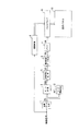
図1は、本発明による駆動方法に基づいて画像表示を行う表示装置の概略構成を示す図である。 FIG. 1 is a diagram showing a schematic configuration of a display device that displays an image based on a driving method according to the present invention.
図1において、表示パネル10は、各画素に対応した画素セルがマトリクス状に配列された例えばプラズマディスプレイパネルの如き表示デバイスである。
In FIG. 1, a
画素データ生成回路1は、入力映像信号を上記表示パネル10の各画素に対応した例えば8ビットの画素データPDに変換してピーク輝度検出回路2及びデータ変換回路3に供給する。
The pixel
ピーク輝度検出回路2は、1画面分の画素データPD毎に最大の輝度レベルを検出し、その最大輝度レベルを示すピーク輝度信号PKをデータ変換回路3及び駆動制御回路4に供給する。
The peak
データ変換回路3は、0〜255なる範囲にて輝度レベルを表現し得る8ビットの画素データPDを、図2(a)、図2(b)又は図2(c)にて示される変換特性にて0〜160なる輝度レベルを表現し得る8ビットの画素データPDDに変換して多階調化処理回路5に供給する。この際、データ変換回路3は、ピーク輝度信号PKが所定の第1ピーク閾値P0よりも大なる輝度レベルを示す場合には図2(a)にて示される変換特性にてデータ変換を行う。又、データ変換回路3は、ピーク輝度信号PKが、第1ピーク閾値P0よりも小であり且つ第2ピーク閾値P1よりも大なる輝度レベルを示す場合には図2(b)、第2ピーク閾値P1よりも小なる輝度レベルを示す場合には図2(c)にて示される変換特性にてデータ変換を行う。尚、図2(c)に示す変換特性は図2(b)に示す変換特性に比べて、中輝度部を中心とした輝度増加率が高くなっている。又、図2(b)に示す変換特性は図2(a)に示す変換特性に比べて、中輝度部を中心とした輝度増加率が高くなっている。すなわち、データ変換回路3は、1画面分の画像のピーク輝度が低いほど、輝度を増加させるべき変換を画素データPDに対して施すのである。
The
多階調化処理回路5は、画素データPDDに対して誤差拡散処理及びディザ処理等を施すことにより、視覚上における輝度の階調表現数を略256階調に維持しつつもそのビット数を4ビットに圧縮した多階調化画素データDSを生成して画素駆動データ生成回路6に供給する。先ず、上記誤差拡散処理では、画素データPDDの上位6ビット分を表示データ、残りの下位2ビット分を誤差データとして夫々分離する。そして、周辺画素各々に対応した画素データPDDにおける上記誤差データを夫々重み付け加算したものを、上記表示データに反映させるようにしている。かかる動作により、原画素における下位2ビット分の輝度が上記周辺画素により擬似的に表現され、それ故に8ビットよりも少ないビット数、すなわち6ビット分の表示データにて、上記8ビット分の画素データと同等の輝度階調表現が可能になるのである。次に、かかる誤差拡散処理によって得られた6ビットの誤差拡散処理後の画素データにディザ処理を施す。例えば、ディザ処理においては、左右、上下に互いに隣接する4つの画素を1組とし、この1組の各画素に対応した画素データ各々に、互いに異なる係数値からなる4つのディザ係数を夫々割り当てて加算する。かかるディザ処理により、この誤差拡散処理後の画素データと同等な輝度階調レベルを維持しつつもそのビット数を図3に示す如き4ビット([0000]〜[1010]なる11通り)に減らした多階調化画素データDSが生成される。
The
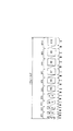
画素駆動データ生成回路6は、かかる多階調化画素データDSを、図3に示す如き変換テーブルに従って各画素の駆動を為す10ビット(第1〜第10ビット)の画素駆動データGDに変換し、これをメモリ7に供給する。尚、図3において、「*」印は論理レベル1又は0のいずれでも良いことを示す。
The pixel drive
メモリ7は、画素駆動データGDを順次書き込み、1画面分の書き込みが終了すると、メモリ7は、この1画面分の画素駆動データGDを各ビット桁毎に分離した、
DB1:GDの第1ビット目
DB2:GDの第2ビット目
DB3:GDの第3ビット目
DB4:GDの第4ビット目
DB5:GDの第5ビット目
DB6:GDの第6ビット目
DB7:GDの第7ビット目
DB8:GDの第8ビット目
DB9:GDの第9ビット目
DB10:GDの第10ビット目
なる画素駆動データビットDB1〜DB10を、夫々に対応したサブフィールドSF1〜SF10(図4に示す)にて読み出してパネルドライバ8に供給する。
The
DB1: 1st bit of GD
DB2: 2nd bit of GD
DB3: 3rd bit of GD
DB4: 4th bit of GD
DB5: 5th bit of GD
DB6: 6th bit of GD
DB7: 7th bit of GD
DB8: 8th bit of GD
DB9: 9th bit of GD
DB10: Pixel drive data bits DB1 to DB10 as the 10th bit of GD are read in corresponding subfields SF1 to SF10 (shown in FIG. 4) and supplied to the
駆動制御回路4は、表示パネル10を図4に示す如きサブフィールド法(サブフレーム法)を採用した発光駆動シーケンスに従って駆動させるべき各種制御信号をパネルドライバ8に供給する。パネルドライバ8は、図4に示す発光駆動シーケンスに従って表示パネル10を駆動すべき各種駆動パルスを生成して表示パネル10に供給する。
The
図4に示す発光駆動シーケンスでは、1フィールド(1フレーム)の表示期間内のサブフィールドSF1〜SF10各々毎に、アドレス行程W及びサスティン行程Iを夫々実行する。又、先頭のサブフィールドSF1に限り、アドレス行程Wに先立ち、リセット行程Rを実行する。 In the light emission drive sequence shown in FIG. 4, the address process W and the sustain process I are executed for each of the subfields SF1 to SF10 in the display period of one field (one frame). Further, the reset process R is executed before the address process W only in the first subfield SF1.
上記リセット行程Rでは、パネルドライバ8は、表示パネル10の全ての画素セルをサスティン行程Iにて発光することが可能な点灯モード状態に初期化すべきリセットパルスを、全ての画素セルに印加する。尚、かかるサスティン行程Iにおいて発光することができない状態を消灯モード状態と称する。
In the reset process R, the
サブフィールドSF1〜SF10各々のアドレス行程Wでは、パネルドライバ8は、そのサブフィールドに対応した画素駆動データビットDBの論理レベルに応じたパルス電圧を有する画素データパルスを各画素セルに印加する。これにより、例えば、画素駆動データビットDBが論理レベル1である場合には、その画素駆動データビットに対応した画素セルに対して高電圧の画素データパルスが印加され、この画素セルは上記点灯モードから消灯モードに推移する。一方、画素駆動データビットDBが論理レベル0である場合には、その画素駆動データビットに対応した画素セルに対して低電圧の画素データパルスが印加され、この画素セルは現在の状態(点灯モード又は消灯モード)を維持する。
In the address process W of each of the subfields SF1 to SF10, the
サブフィールドSF1〜SF10各々のサスティン行程Iでは、パネルドライバ8は、そのサブフィールドに割り当てられている回数(期間)Kだけ上記点灯モード状態に設定されている画素セルのみを繰り返し発光させるべきサスティンパルスを全ての画素セルに印加する。
In the sustain process I of each of the subfields SF1 to SF10, the
上記駆動によれば、サブフィールドSF1〜SF10において、画素セルを消灯モード状態から点灯モード状態に推移できる機会は、先頭のサブフィールドSF1のリセット行程Rだけである。よって、図3に示す如き11通りの画素駆動データGDによれば、サブフィールドSF1のリセット行程Rにて点灯モードに初期化された画素セルは、SF1〜SF10の内の1のサブフィールド(黒丸印にて示す)のアドレス行程Wにおいて消灯モードに設定されるまでの間、点灯モードを維持する。従って、その間に存在するサブフィールド各々(白丸にて示す)のサスティン行程Iにおいて、各サブフィールドに割り当てられている回数(又は期間)だけ画素セルが発光することになる。この際、1フィールドを通してサブフィールドSF1〜SF10各々のサスティン行程Iにて実施された発光の合計回数に対応した中間輝度が視覚されることになる。すなわち、図3に示す如き11通りの画素駆動データGDに応じて、互いに異なる中間輝度を11段階にて表現し得る第1〜第11階調駆動が為されるのである。 According to the driving described above, in the subfields SF1 to SF10, the opportunity to change the pixel cell from the extinguishing mode state to the lighting mode state is only the reset process R of the first subfield SF1. Therefore, according to 11 types of pixel drive data GD as shown in FIG. 3, the pixel cell initialized to the lighting mode in the reset process R of the subfield SF1 is one subfield (black circle) of SF1 to SF10. The lighting mode is maintained until the extinguishing mode is set in the address process W (shown by a mark). Therefore, in the sustain process I of each subfield existing between them (indicated by white circles), the pixel cell emits light for the number of times (or period) assigned to each subfield. At this time, intermediate luminance corresponding to the total number of times of light emission performed in the sustain process I of each of the subfields SF1 to SF10 through one field is visually recognized. That is, the first to eleventh gradation driving capable of expressing 11 different intermediate luminances in 11 steps is performed according to 11 types of pixel drive data GD as shown in FIG.
ここで、11通りの画素駆動データGDは、図3に示す如く、多階調化画素データDSに対応している。又、かかる多階調化画素データDSは、データ変換回路3によって変換出力された画素データPDDに対して多階調化処理を施して得られたものである。この際、画素データPDDにて示される輝度レベルが「0」の場合には[0000]なる多階調化画素データDSが生成されるものとする。更に、画素データPDDにて示される輝度レベルが、
「1」〜「16」の場合には[0001]、
「17」〜「32」の場合には[0010]、
「33」〜「48」の場合には[0011]、
「49」〜「64」の場合には[0100]、
「65」〜「80」の場合には[0101]、
「81」〜「96」の場合には[0110]、
「97」〜「112」の場合には[0111]、
「113」〜「128」の場合には[1000]、
「129」〜「144」の場合には[1001]、
「145」〜「160」の場合には[1010]、
なる4ビットの多階調化画素データDSが夫々生成されるものとする。
Here, the 11 types of pixel drive data GD correspond to the multi-gradation pixel data DS as shown in FIG. The multi-gradation pixel data DS is obtained by performing multi-gradation processing on the pixel data PDD converted and output by the
In the case of “1” to “16”, [0001]
In the case of “17” to “32”, [0010]
In the case of “33” to “48”, [0011]
In the case of “49” to “64”, [0100],
In the case of “65” to “80”, [0101]
In the case of “81” to “96”, [0110]
In the case of “97” to “112”, [0111]
In the case of “113” to “128”, [1000]
In the case of “129” to “144”, [1001]
In the case of “145” to “160”, [1010]
It is assumed that 4-bit multi-gradation pixel data DS is generated.
これによると、画素データPDDにて示される輝度レベルが「0」の場合には、図3に示す第1階調駆動が実施され、サブフィールドSF1〜SF10を通して画素セルが全く発光しない、いわゆる黒表示が為される。又、画素データPDDにて示される輝度レベルが「1」〜「16」なる範囲内にある場合には、図3に示す第2階調駆動が実施され、サブフィールドSF1〜SF10の内のSF1のみで画素セルの発光が為される。又、画素データPDDにて示される輝度レベルが「17」〜「32」なる範囲内にある場合には、図3に示す第3階調駆動が実施され、サブフィールドSF1〜SF10の内のSF1及びSF2のみで夫々画素セルの発光が為される。同様に、画素データPDDにて示される輝度レベルが、
「33」〜「48」の場合にはSF1〜SF3、
「49」〜「64」の場合にはSF1〜SF4、
「65」〜「80」の場合にはSF1〜SF5、
「81」〜「96」の場合にはSF1〜SF6、
「97」〜「112」の場合にはSF1〜SF7、
「113」〜「128」の場合にはSF1〜SF8、
「129」〜「144」の場合にはSF1〜SF9、
「145」〜「160」の場合にはSF1〜SF10、
にて夫々、連続して画素セルの発光が為される。
According to this, when the luminance level indicated by the pixel data PDD is “0”, the first gradation drive shown in FIG. Display is made. When the luminance level indicated by the pixel data PDD is in the range of “1” to “16”, the second gradation drive shown in FIG. 3 is performed, and SF1 in the subfields SF1 to SF10 is performed. Only the pixel cell emits light. When the luminance level indicated by the pixel data PDD is in the range of “17” to “32”, the third gradation drive shown in FIG. 3 is performed, and SF1 in the subfields SF1 to SF10 is executed. And the light emission of each pixel cell is performed only by SF2. Similarly, the luminance level indicated by the pixel data PDD is
In the case of “33” to “48”, SF1 to SF3,
In the case of “49” to “64”, SF1 to SF4,
In the case of “65” to “80”, SF1 to SF5,
In the case of “81” to “96”, SF1 to SF6,
In the case of “97” to “112”, SF1 to SF7,
In the case of “113” to “128”, SF1 to SF8,
In the case of “129” to “144”, SF1 to SF9,
In the case of “145” to “160”, SF1 to SF10,
Each of the pixel cells emits light continuously.
この際、画素データPDDは、入力映像信号に基づく画素データPDに対して図2(a)、図2(b)又は図2(c)に示す変換特性にてデータ変換を施して得られたものである。 At this time, the pixel data PDD is obtained by subjecting the pixel data PD based on the input video signal to data conversion with the conversion characteristics shown in FIG. 2A, FIG. 2B, or FIG. Is.
すなわち、入力映像信号に基づく1画面分の画像におけるピーク輝度が比較的高い場合(ピーク輝度信号PK>第1ピーク閾値P0)には、図2(a)に示す変換特性に基づき、画素データPDが画素データPDDに変換される。この際、図2(a)に示す如き変換特性によれば、例えば輝度レベル「127」以下の低輝度を表す画素データPD(入力映像信号)に対しては、第1〜第7階調駆動による7階調分の階調駆動が為される。 That is, when the peak luminance in the image for one screen based on the input video signal is relatively high (peak luminance signal PK> first peak threshold value P0), the pixel data PD is based on the conversion characteristics shown in FIG. Are converted into pixel data PDD. At this time, according to the conversion characteristics as shown in FIG. 2A, for example, pixel data PD (input video signal) representing low luminance of luminance level “127” or lower is driven in the first to seventh gradations. The gradation drive for 7 gradations is performed.
又、入力映像信号に基づく1画面分の画像におけるピーク輝度が中程度である場合(第2ピーク閾値P1<ピーク輝度信号PK<第1ピーク閾値P0)には、図2(b)に示す変換特性に基づき、画素データPDが画素データPDDに変換される。この際、図2(b)に示す如き変換特性によれば、例えば輝度レベル「127」以下の低輝度を表す画素データPD(入力映像信号)に対しては、第1〜第8階調駆動による8階調分の階調駆動が為される。 When the peak luminance in the image for one screen based on the input video signal is medium (second peak threshold P1 <peak luminance signal PK <first peak threshold P0), the conversion shown in FIG. Based on the characteristics, the pixel data PD is converted into pixel data PDD. At this time, according to the conversion characteristics as shown in FIG. 2B, for example, pixel data PD (input video signal) representing low luminance below the luminance level “127” is driven in the first to eighth gradations. The gradation driving for 8 gradations is performed.
又、入力映像信号に基づく1画面分の画像におけるピーク輝度が比較的低い場合(第2ピーク閾値P1>ピーク輝度信号PK)には、図2(c)に示す変換特性に基づき、画素データPDが画素データPDDに変換される。この際、図2(c)に示す如き変換特性によれば、例えば輝度レベル「127」以下の低輝度を表す画素データPD(入力映像信号)に対しては、第1〜第9階調駆動による9階調分の階調駆動が為される。 When the peak luminance in the image for one screen based on the input video signal is relatively low (second peak threshold P1> peak luminance signal PK), the pixel data PD is based on the conversion characteristics shown in FIG. Are converted into pixel data PDD. At this time, according to the conversion characteristics as shown in FIG. 2C, for example, pixel data PD (input video signal) representing low luminance below the luminance level “127” is driven in the first to ninth gradations. The gradation drive for 9 gradations is performed.
すなわち、図2(a)〜図2(c)に示す如きデータ変換により、1画面分の画像中のピーク輝度が低いほど、入力映像信号中における低輝度成分の表示を担うサブフィールドの数を増加させて、この低輝度成分に対する階調数を増やすのである。この際、1フィールド内におけるサブフィールドの数、及び各階調駆動による1フィールド内での発光の合計回数(期間)は、上記ピーク輝度に拘わらず一定である。 That is, by the data conversion as shown in FIG. 2A to FIG. 2C, the lower the peak luminance in the image for one screen, the lower the number of subfields responsible for displaying the low luminance component in the input video signal. The number of gradations for this low luminance component is increased. At this time, the number of subfields in one field and the total number of times (period) of light emission in one field by each gradation drive are constant regardless of the peak luminance.
従って、上記の如き駆動によれば、低輝度部に対する画像品質を落とすことなく、輝度を高めることが可能となる。 Therefore, according to the driving as described above, it is possible to increase the luminance without degrading the image quality for the low luminance portion.
2 ピーク輝度検出回路
3 データ変換回路
4 駆動制御回路
10 表示パネル
2 Peak
Claims (3)
各フィールド内において入力映像信号によって示される輝度レベルに応じた個数のサブフィールド各々にて前記画素セルの発光を実行させる行程と、
1フィールド分の前記入力映像信号におけるピーク輝度レベルに応じて、前記入力映像信号中の所定輝度よりも低輝度な輝度レベルに対して割り当てるべき前記サブフィールドの個数を変更することにより、各フィールド内において前記画素セルを発光させる発光回数又は発光期間を制御する行程と、を有することを特徴とする表示パネルの駆動方法。 A display panel driving method for driving a display panel in which a plurality of pixel cells are formed for each of a plurality of subfields to which the number of times or a period for which the pixel cells are to be emitted is assigned.
A step of executing light emission of the pixel cell in each of a number of subfields corresponding to a luminance level indicated by an input video signal in each field;
By changing the number of subfields to be assigned to a luminance level lower than a predetermined luminance in the input video signal according to a peak luminance level in the input video signal for one field, And a step of controlling a light emission frequency or a light emission period for causing the pixel cell to emit light.
Priority Applications (3)
| Application Number | Priority Date | Filing Date | Title |
|---|---|---|---|
| JP2004111848A JP2005300569A (en) | 2004-04-06 | 2004-04-06 | Method for driving display panel |
| EP05007191A EP1585093A3 (en) | 2004-04-06 | 2005-04-01 | Driving method of an electroluminescent or plasma display panel |
| US11/099,702 US7576714B2 (en) | 2004-04-06 | 2005-04-06 | Display-panel driving method |
Applications Claiming Priority (1)
| Application Number | Priority Date | Filing Date | Title |
|---|---|---|---|
| JP2004111848A JP2005300569A (en) | 2004-04-06 | 2004-04-06 | Method for driving display panel |
Publications (1)
| Publication Number | Publication Date |
|---|---|
| JP2005300569A true JP2005300569A (en) | 2005-10-27 |
Family
ID=34909486
Family Applications (1)
| Application Number | Title | Priority Date | Filing Date |
|---|---|---|---|
| JP2004111848A Pending JP2005300569A (en) | 2004-04-06 | 2004-04-06 | Method for driving display panel |
Country Status (3)
| Country | Link |
|---|---|
| US (1) | US7576714B2 (en) |
| EP (1) | EP1585093A3 (en) |
| JP (1) | JP2005300569A (en) |
Cited By (1)
| Publication number | Priority date | Publication date | Assignee | Title |
|---|---|---|---|---|
| JP2008122517A (en) * | 2006-11-09 | 2008-05-29 | Eastman Kodak Co | Data driver and display device |
Families Citing this family (2)
| Publication number | Priority date | Publication date | Assignee | Title |
|---|---|---|---|---|
| US20150049122A1 (en) * | 2013-08-19 | 2015-02-19 | Pixtronix, Inc. | Display Apparatus Configured For Image Formation With Variable Subframes |
| KR102074719B1 (en) * | 2013-10-08 | 2020-02-07 | 엘지디스플레이 주식회사 | Organic light emitting display device |
Citations (10)
| Publication number | Priority date | Publication date | Assignee | Title |
|---|---|---|---|---|
| JPH0514840A (en) * | 1991-07-05 | 1993-01-22 | Sanyo Electric Co Ltd | Video signal processing circuit |
| JPH06160811A (en) * | 1992-11-26 | 1994-06-07 | Sanyo Electric Co Ltd | Liquid crystal projector |
| JPH0738829A (en) * | 1993-07-21 | 1995-02-07 | Sanyo Electric Co Ltd | Contrast control circuit and liquid crystal projector using same |
| JP2000013814A (en) * | 1998-06-19 | 2000-01-14 | Pioneer Electron Corp | Video signal processing circuit |
| JP2002366121A (en) * | 2001-06-12 | 2002-12-20 | Matsushita Electric Ind Co Ltd | Video display device and video display method |
| JP2002366093A (en) * | 2001-06-12 | 2002-12-20 | Pioneer Electronic Corp | Display device |
| JP2003167544A (en) * | 2001-11-29 | 2003-06-13 | Sony Corp | Video display and video signal processing method |
| JP2003177697A (en) * | 2001-12-12 | 2003-06-27 | Mitsubishi Electric Corp | Video display device |
| JP2003186111A (en) * | 2001-12-14 | 2003-07-03 | Seiko Epson Corp | Illuminator, projector and driving method therefor |
| JP2004054250A (en) * | 2002-05-29 | 2004-02-19 | Matsushita Electric Ind Co Ltd | Image display method and device therefor |
Family Cites Families (9)
| Publication number | Priority date | Publication date | Assignee | Title |
|---|---|---|---|---|
| JP4802350B2 (en) * | 1998-03-12 | 2011-10-26 | ソニー株式会社 | Display device |
| JP2994630B2 (en) * | 1997-12-10 | 1999-12-27 | 松下電器産業株式会社 | Display device capable of adjusting the number of subfields by brightness |
| JP3805126B2 (en) * | 1999-03-04 | 2006-08-02 | パイオニア株式会社 | Driving method of display panel |
| JP4484276B2 (en) * | 1999-09-17 | 2010-06-16 | 日立プラズマディスプレイ株式会社 | Plasma display device and display method thereof |
| JP2001195035A (en) * | 2000-01-14 | 2001-07-19 | Fujitsu General Ltd | Contrast adjusting circuit |
| US6633343B2 (en) * | 2000-03-14 | 2003-10-14 | Matsushita Electric Industrial Co., Ltd. | Dynamic gamma correction apparatus |
| JP3767791B2 (en) * | 2000-04-18 | 2006-04-19 | パイオニア株式会社 | Driving method of display panel |
| JP3487259B2 (en) * | 2000-05-22 | 2004-01-13 | 日本電気株式会社 | Video display device and display method thereof |
| JP2001350447A (en) * | 2000-06-06 | 2001-12-21 | Pioneer Electronic Corp | Driving method for plasma display panel |
-
2004
- 2004-04-06 JP JP2004111848A patent/JP2005300569A/en active Pending
-
2005
- 2005-04-01 EP EP05007191A patent/EP1585093A3/en not_active Withdrawn
- 2005-04-06 US US11/099,702 patent/US7576714B2/en not_active Expired - Fee Related
Patent Citations (10)
| Publication number | Priority date | Publication date | Assignee | Title |
|---|---|---|---|---|
| JPH0514840A (en) * | 1991-07-05 | 1993-01-22 | Sanyo Electric Co Ltd | Video signal processing circuit |
| JPH06160811A (en) * | 1992-11-26 | 1994-06-07 | Sanyo Electric Co Ltd | Liquid crystal projector |
| JPH0738829A (en) * | 1993-07-21 | 1995-02-07 | Sanyo Electric Co Ltd | Contrast control circuit and liquid crystal projector using same |
| JP2000013814A (en) * | 1998-06-19 | 2000-01-14 | Pioneer Electron Corp | Video signal processing circuit |
| JP2002366121A (en) * | 2001-06-12 | 2002-12-20 | Matsushita Electric Ind Co Ltd | Video display device and video display method |
| JP2002366093A (en) * | 2001-06-12 | 2002-12-20 | Pioneer Electronic Corp | Display device |
| JP2003167544A (en) * | 2001-11-29 | 2003-06-13 | Sony Corp | Video display and video signal processing method |
| JP2003177697A (en) * | 2001-12-12 | 2003-06-27 | Mitsubishi Electric Corp | Video display device |
| JP2003186111A (en) * | 2001-12-14 | 2003-07-03 | Seiko Epson Corp | Illuminator, projector and driving method therefor |
| JP2004054250A (en) * | 2002-05-29 | 2004-02-19 | Matsushita Electric Ind Co Ltd | Image display method and device therefor |
Cited By (1)
| Publication number | Priority date | Publication date | Assignee | Title |
|---|---|---|---|---|
| JP2008122517A (en) * | 2006-11-09 | 2008-05-29 | Eastman Kodak Co | Data driver and display device |
Also Published As
| Publication number | Publication date |
|---|---|
| US20050259043A1 (en) | 2005-11-24 |
| EP1585093A2 (en) | 2005-10-12 |
| US7576714B2 (en) | 2009-08-18 |
| EP1585093A3 (en) | 2006-01-04 |
Similar Documents
| Publication | Publication Date | Title |
|---|---|---|
| JP3767791B2 (en) | Driving method of display panel | |
| KR100701098B1 (en) | Method for power level control of a display device and apparatus for carrying out the method | |
| JP3805126B2 (en) | Driving method of display panel | |
| JP3736671B2 (en) | Driving method of plasma display panel | |
| JP2003015588A (en) | Display device | |
| JP2002366086A (en) | Method for driving plasma display panel and plasma display device | |
| JP4170713B2 (en) | Driving method of display panel | |
| JP3961171B2 (en) | Multi-tone processing circuit for display device | |
| JP2006113517A (en) | Plasma display device and method for driving same | |
| JP4146126B2 (en) | Driving method of plasma display panel | |
| JP2000231362A (en) | Driving method for plasma display panel | |
| JP2000259121A (en) | Display panel driving method | |
| JP4703892B2 (en) | Driving method of display panel | |
| JP3734244B2 (en) | Driving method of display panel | |
| JP2003022045A (en) | Driving method of plasma display panel | |
| US7576714B2 (en) | Display-panel driving method | |
| JP4165108B2 (en) | Plasma display device | |
| JP4541025B2 (en) | Driving method of display panel | |
| JP4679932B2 (en) | Driving method of display panel | |
| JP4731738B2 (en) | Display device | |
| JP4828994B2 (en) | Driving method of plasma display panel | |
| JP2008209590A (en) | Driving device of display panel | |
| JP2006053547A (en) | Plasma display device and its driving method | |
| JP4731841B2 (en) | Display panel driving apparatus and driving method | |
| JP2006343377A (en) | Display apparatus |
Legal Events
| Date | Code | Title | Description |
|---|---|---|---|
| A621 | Written request for application examination |
Free format text: JAPANESE INTERMEDIATE CODE: A621 Effective date: 20070320 |
|
| A711 | Notification of change in applicant |
Free format text: JAPANESE INTERMEDIATE CODE: A711 Effective date: 20090605 |
|
| A977 | Report on retrieval |
Free format text: JAPANESE INTERMEDIATE CODE: A971007 Effective date: 20090831 |
|
| A131 | Notification of reasons for refusal |
Free format text: JAPANESE INTERMEDIATE CODE: A131 Effective date: 20090915 |
|
| A521 | Written amendment |
Free format text: JAPANESE INTERMEDIATE CODE: A523 Effective date: 20091110 |
|
| A131 | Notification of reasons for refusal |
Free format text: JAPANESE INTERMEDIATE CODE: A131 Effective date: 20100126 |
|
| A02 | Decision of refusal |
Free format text: JAPANESE INTERMEDIATE CODE: A02 Effective date: 20100706 |