JP2005287140A - Switching power supply circuit - Google Patents
Switching power supply circuit Download PDFInfo
- Publication number
- JP2005287140A JP2005287140A JP2004095278A JP2004095278A JP2005287140A JP 2005287140 A JP2005287140 A JP 2005287140A JP 2004095278 A JP2004095278 A JP 2004095278A JP 2004095278 A JP2004095278 A JP 2004095278A JP 2005287140 A JP2005287140 A JP 2005287140A
- Authority
- JP
- Japan
- Prior art keywords
- voltage
- switching
- circuit
- winding
- current
- Prior art date
- Legal status (The legal status is an assumption and is not a legal conclusion. Google has not performed a legal analysis and makes no representation as to the accuracy of the status listed.)
- Pending
Links
Images


Classifications
-
- Y—GENERAL TAGGING OF NEW TECHNOLOGICAL DEVELOPMENTS; GENERAL TAGGING OF CROSS-SECTIONAL TECHNOLOGIES SPANNING OVER SEVERAL SECTIONS OF THE IPC; TECHNICAL SUBJECTS COVERED BY FORMER USPC CROSS-REFERENCE ART COLLECTIONS [XRACs] AND DIGESTS
- Y02—TECHNOLOGIES OR APPLICATIONS FOR MITIGATION OR ADAPTATION AGAINST CLIMATE CHANGE
- Y02P—CLIMATE CHANGE MITIGATION TECHNOLOGIES IN THE PRODUCTION OR PROCESSING OF GOODS
- Y02P80/00—Climate change mitigation technologies for sector-wide applications
- Y02P80/10—Efficient use of energy, e.g. using compressed air or pressurized fluid as energy carrier
Abstract
Description
本発明は、力率改善回路を備えたスイッチング電源回路に関するものである。 The present invention relates to a switching power supply circuit including a power factor correction circuit.
先に本出願人は、一次側に共振形コンバータを備えた電源回路を各種提案している。また、共振形コンバータに対して力率改善を図るための力率改善回路を備えて構成した電源回路も各種提案している。
図10は、先に本出願人により出願された発明に基づいて構成される、力率改善機能を有するスイッチング電源回路の一例を示す回路図である。
The present applicant has previously proposed various power supply circuits having a resonance type converter on the primary side. Various power supply circuits configured with a power factor correction circuit for improving the power factor of the resonant converter have also been proposed.
FIG. 10 is a circuit diagram showing an example of a switching power supply circuit having a power factor correction function, which is configured based on the invention previously filed by the present applicant.
図10に示す電源回路は、他励式による電流共振形のスイッチングコンバータに対して力率改善回路20を備えた構成を採る。この電源回路におけるスイッチングコンバータは、ハーフブリッジ結合方式による電流共振形コンバータと、半導体スイッチ(スイッチング素子)のターンオフ時にのみ電圧共振する部分電圧共振回路を組み合わせたスイッチングコンバータとされている。 The power supply circuit shown in FIG. 10 employs a configuration in which a power factor correction circuit 20 is provided for a separately-excited current resonance type switching converter. The switching converter in this power supply circuit is a switching converter that combines a current resonance type converter using a half-bridge coupling method and a partial voltage resonance circuit that performs voltage resonance only when the semiconductor switch (switching element) is turned off.
この図10に示す電源回路においては、先ず、商用交流電源ACに対し、2組のフィルタコンデンサCL、CL及び1組のコモンモードチョークコイルCMCから成るコモンモードノイズフィルタが接続されている。
そして、商用交流電源ACから直流入力電圧を生成する整流平滑回路としては、上記コモンモードノイズフィルタの後段に対して、ブリッジ整流回路Di及び平滑コンデンサCiとから成る全波整流回路が備えられる。
この場合、ブリッジ整流回路Diの全波整流動作により得られた整流出力は、力率改善回路20を介して平滑コンデンサCiに充電される。これにより、平滑コンデンサCiの両端には、交流入力電圧VACの等倍のレベルに対応する整流平滑電圧Ei(直流入力電圧)が得られることになる。
力率改善回路20については後述する。
In the power supply circuit shown in FIG. 10, first, a common mode noise filter including two sets of filter capacitors CL and CL and one set of common mode choke coil CMC is connected to commercial AC power supply AC.
As a rectifying / smoothing circuit for generating a DC input voltage from the commercial AC power supply AC, a full-wave rectifying circuit including a bridge rectifying circuit Di and a smoothing capacitor Ci is provided for the subsequent stage of the common mode noise filter.
In this case, the rectified output obtained by the full-wave rectification operation of the bridge rectifier circuit Di is charged to the smoothing capacitor Ci via the power factor correction circuit 20. As a result, a rectified and smoothed voltage Ei (DC input voltage) corresponding to a level equal to the AC input voltage VAC is obtained at both ends of the smoothing capacitor Ci.
The power factor correction circuit 20 will be described later.
上記直流入力電圧を入力してスイッチングする電流共振形コンバータとしては、図示するようにして、MOS−FETによる2本のスイッチング素子Q1,Q2をハーフブリッジ結合により接続している。スイッチング素子Q1,Q2の各ドレイン−ソース間に対しては、図示する方向により、それぞれボディダイオードによるダンパーダイオードDD1,DD2が並列に接続される。 As shown in the figure, as the current resonance type converter for switching by inputting the DC input voltage, two switching elements Q1, Q2 by MOS-FETs are connected by half bridge coupling. Damper diodes DD1 and DD2 formed of body diodes are connected in parallel with each other between the drains and sources of the switching elements Q1 and Q2, respectively, in the direction shown in the drawing.
また、スイッチング素子Q2のドレイン−ソース間に対しては、部分共振コンデンサCpが並列に接続される。この部分共振コンデンサCpのキャパシタンスと一次巻線N1のリーケージインダクタンスL1によっては並列共振回路(部分電圧共振回路)を形成する。そして、スイッチング素子Q1,Q2のターンオフ時にのみ電圧共振する、部分電圧共振動作が得られるようになっている。 A partial resonance capacitor Cp is connected in parallel between the drain and source of the switching element Q2. A parallel resonance circuit (partial voltage resonance circuit) is formed by the capacitance of the partial resonance capacitor Cp and the leakage inductance L1 of the primary winding N1. A partial voltage resonance operation in which voltage resonance occurs only when the switching elements Q1, Q2 are turned off is obtained.
この電源回路においては、スイッチング素子Q1,Q2をスイッチング駆動するために、例えば汎用のICによる発振・ドライブ回路2が設けられる。この発振・ドライブ回路2は、発振回路、駆動回路を有している。そして、発振回路及び駆動回路によって、所要の周波数によるドライブ信号(ゲート電圧)をスイッチング素子Q1,Q2の各ゲートに対して印加する。これにより、スイッチング素子Q1,Q2は、所要のスイッチング周波数により交互にオン/オフするようにしてスイッチング動作を行う。
In this power supply circuit, in order to switch the switching elements Q1 and Q2, for example, an oscillation /
絶縁コンバータトランスPIT (Power Isolation Transformer)は、スイッチング素子Q1 、Q2 のスイッチング出力を二次側に伝送する。
この絶縁コンバータトランスPITの一次巻線N1 の一端は、スイッチング素子Q1 のソースとスイッチング素子Q2 のドレインの接続点(スイッチング出力点)に接続されることで、スイッチング出力が得られるようにされる。
また、一次巻線N1 の他端は、直列共振コンデンサC1 を介するようにして、力率改善回路20内の高速リカバリ型ダイオードD1のカソードと高周波インダクタL10の接続点に対して接続されている。
An insulating converter transformer PIT (Power Isolation Transformer) transmits the switching outputs of the switching elements Q1 and Q2 to the secondary side.
One end of the primary winding N1 of the insulating converter transformer PIT is connected to a connection point (switching output point) between the source of the switching element Q1 and the drain of the switching element Q2, thereby obtaining a switching output.
The other end of the primary winding N1 is connected to the connection point between the cathode of the fast recovery diode D1 and the high frequency inductor L10 in the power factor correction circuit 20 through the series resonant capacitor C1.
この場合、直列共振コンデンサC1 及び一次巻線N1 は直列に接続されているが、この直列共振コンデンサC1 のキャパシタンス、及び一次巻線N1 (直列共振巻線)を含む絶縁コンバータトランスPITの漏洩インダクタンス(リーケージインダクタンス)成分L1により、スイッチングコンバータの動作を電流共振形とするための一次側直列共振回路を形成している。 In this case, the series resonant capacitor C1 and the primary winding N1 are connected in series, but the capacitance of the series resonant capacitor C1 and the leakage inductance of the insulating converter transformer PIT including the primary winding N1 (series resonant winding) ( The primary side series resonance circuit for making the operation of the switching converter into a current resonance type is formed by the leakage inductance component L1.
上記説明によると、この図に示す一次側スイッチングコンバータとしては、一次側直列共振回路(L1−C1)による電流共振形としての動作と、前述した部分電圧共振回路(Cp//L1)とによる部分電圧共振動作とが得られることになる。
つまり、この図に示す電源回路は、一次側スイッチングコンバータを共振形とするための共振回路に対して、他の共振回路とが組み合わされた形式を採っていることになる。本明細書では、このようなスイッチングコンバータについて、複合共振形コンバータということにする。
According to the above description, the primary side switching converter shown in this figure has the operation as the current resonance type by the primary side series resonance circuit (L1-C1) and the part by the partial voltage resonance circuit (Cp // L1) described above. A voltage resonance operation is obtained.
That is, the power supply circuit shown in this figure adopts a form in which a resonance circuit for making the primary side switching converter a resonance type is combined with another resonance circuit. In this specification, such a switching converter is referred to as a composite resonance type converter.
ここでの図示による説明は省略するが、絶縁コンバータトランスPITの構造としては、例えばフェライト材によるE型コアを組み合わせたEE型コアを備える。そして、一次側と二次側とで巻装部位を分割したうえで、一次巻線N1と、二次巻線N2(N2A,N2B)を、EE型コアの中央磁脚に対して巻装している。 Although illustration explanation here is omitted, the structure of the insulating converter transformer PIT includes, for example, an EE type core in which an E type core made of a ferrite material is combined. Then, after the winding part is divided on the primary side and the secondary side, the primary winding N1 and the secondary winding N2 (N2A, N2B) are wound around the central magnetic leg of the EE type core. ing.
絶縁コンバータトランスPITの二次巻線N2としては、センタータップが施されたことで2つに分割された、同じ所定巻数による二次巻線N2A,N2Bが巻装されている。これらの二次巻線N2A,N2Bには、一次巻線N1に伝達されたスイッチング出力に応じた交番電圧が励起される。 As the secondary winding N2 of the insulating converter transformer PIT, secondary windings N2A and N2B having the same predetermined number of turns, which are divided into two by the center tap, are wound. An alternating voltage corresponding to the switching output transmitted to the primary winding N1 is excited in these secondary windings N2A and N2B.
そして、これら二次巻線N2A,N2Bに対しては、図示するように整流用素子としてNチャネルのMOS−FETQ3,Q4,Q5,Q6、ゲート抵抗Rg1,Rg2、及び二次側平滑コンデンサCoを備えて形成される、巻線電圧検出方式による同期整流回路が接続される。なお、MOS−FETQ3,Q4、Q5、Q6のドレイン−ソースに対しては、それぞれ、ボディダイオードDD3,DD4、DD5、DD6が並列に接続される。
このようにして形成される同期整流回路では、二次巻線N2に励起される交番電圧が反転するタイミングに応じて、MOS−FETQ3//Q5の組と、MOS−FETQ4//Q6の組が交互にオン/オフするようにして両波整流動作(スイッチング動作)を行う。
For these secondary windings N2A and N2B, N-channel MOS-FETs Q3, Q4, Q5 and Q6, gate resistors Rg1 and Rg2 and a secondary smoothing capacitor Co are provided as rectifying elements as shown in the figure. A synchronous rectifier circuit based on a winding voltage detection method is provided. Note that body diodes DD3, DD4, DD5, and DD6 are connected in parallel to the drain-source of the MOS-FETs Q3, Q4, Q5, and Q6, respectively.
In the synchronous rectifier circuit thus formed, the MOS-FET Q3 // Q5 group and the MOS-FET Q4 // Q6 group are divided according to the timing at which the alternating voltage excited by the secondary winding N2 is inverted. A double-wave rectification operation (switching operation) is performed so as to be alternately turned on and off.
同期整流回路が上記のようにして整流動作を行うことで、平滑コンデンサCoの両端電圧として、二次側直流出力電圧Eoが得られることになる。この二次側直流出力電圧Eoは、負荷に供給されると共に、分岐して制御回路1に対しても入力される。
When the synchronous rectification circuit performs the rectification operation as described above, the secondary side DC output voltage Eo is obtained as the voltage across the smoothing capacitor Co. The secondary side DC output voltage Eo is supplied to the load and is branched and input to the
この場合の制御回路1は、例えば二次側直流出力電圧Eoの変動に対応したレベルの制御信号を発振・ドライブ回路2に出力する。発振・ドライブ回路2では制御回路1から供給された制御信号に基づいて、発振・ドライブ回路2からスイッチング素子Q1,Q2の各ゲートに供給するスイッチング駆動信号の周波数を変化させて、スイッチング周波数を可変するようにしている。このように、二次側直流出力電圧Eoのレベルに応じてスイッチング素子Q1,Q2のスイッチング周波数が可変制御されることで、一次側直列共振回路を形成する一次巻線N1から二次側に伝送されるエネルギーも可変され、二次側直流出力電圧Eoのレベルが可変制御される。これにより、二次側直流出力電圧の定電圧制御が図られることになる。
なお、以降は、上記のようにしてスイッチング周波数を可変制御することによって直流安定化を図る定電圧制御方式を「スイッチング周波数制御方式」ということにする。
In this case, the
Hereinafter, the constant voltage control method for stabilizing the DC voltage by variably controlling the switching frequency as described above will be referred to as a “switching frequency control method”.
なお、図10に示す同期整流回路について、上記のようにして整流素子としてのMOS−FETを並列に接続しているのは、図10の電源回路として実際に対応すべき負荷条件が、例えば二次側直流出力電圧Eo=5Vに対して、負荷電流が30A〜0Aで変動する、いわゆる低電圧/大電流といわれる負荷条件であることに依る。このような負荷条件は、実質的には相当に変動幅が広範囲となるものであり、従って、負荷が重くなる傾向では、二次側整流回路にも相当に大きな電流が流れる。そこで、整流素子であるMOS−FETについて、複数本を並列接続しているものである。 In the synchronous rectifier circuit shown in FIG. 10, the MOS-FETs as rectifier elements are connected in parallel as described above because the load conditions to be actually handled as the power supply circuit in FIG. It depends on the so-called low voltage / large current load condition in which the load current varies between 30 A and 0 A with respect to the secondary DC output voltage Eo = 5V. Such a load condition has a substantially wide fluctuation range. Therefore, when the load is heavy, a considerably large current flows through the secondary side rectifier circuit. Therefore, a plurality of MOS-FETs that are rectifying elements are connected in parallel.
また、この二次側の同期整流回路において、MOS−FETQ3//Q5の組に整流電流が流れる整流電流経路と、MOS−FETQ4//Q6の組に整流電流が流れる整流電流経路とで共通の経路となる、MOS−FETQ3//Q5のソースと、MOS−FETQ4//Q6のソースとの接続点と二次側アースとの間のラインには、電流検出抵抗R1A//R1Bの並列接続回路が直列に挿入される。
なお、この電流検出抵抗R1A,R1Bを含む過電流保護のための構成については後述する。
In this secondary side synchronous rectifier circuit, the rectified current path through which the rectified current flows through the pair of MOS-FETs Q3 // Q5 and the rectified current path through which the rectified current flows through the pair of MOS-FETs Q4 // Q6 are common. In the line between the connection point of the source of the MOS-FET Q3 // Q5 and the source of the MOS-FET Q4 // Q6 and the secondary side ground, which is the path, a parallel connection circuit of the current detection resistors R1A // R1B Are inserted in series.
The configuration for overcurrent protection including the current detection resistors R1A and R1B will be described later.
続いて、力率改善回路20の構成について説明する。
この力率改善回路20は磁気結合形による電力回生方式としての構成を採る。
力率改善回路20においては、ブリッジ整流回路Diの正極出力端子と平滑コンデンサCiの正極端子間に対して、高速リカバリ型ダイオードD1−高周波インダクタL10が直列接続されて挿入される。
フィルタコンデンサCN は高速リカバリ型ダイオードD1 のアノード側と平滑コンデンサCiの正極端子間に対して挿入されることで、ノーマルモードノイズ(スイッチング周期の交番成分)を吸収するフィルタとして機能する。
Next, the configuration of the power factor correction circuit 20 will be described.
The power factor correction circuit 20 employs a configuration as a power regeneration system using a magnetic coupling type.
In the power factor correction circuit 20, a fast recovery type diode D1 and a high frequency inductor L10 are connected in series between the positive output terminal of the bridge rectifier circuit Di and the positive terminal of the smoothing capacitor Ci.
The filter capacitor CN is inserted between the anode side of the fast recovery diode D1 and the positive terminal of the smoothing capacitor Ci, and functions as a filter that absorbs normal mode noise (alternating component of the switching period).
そして力率改善回路20に対しては、高速リカバリ型ダイオードD1 のカソードと高周波インダクタL10の接続点に対して、上述した一次側直列共振回路(C1−N1(L1))が接続されて、この直列共振回路に得られるスイッチング出力が帰還されるようにしている。 The power factor correction circuit 20 is connected to the above-described primary side series resonance circuit (C1-N1 (L1)) at the connection point between the cathode of the fast recovery diode D1 and the high frequency inductor L10. The switching output obtained in the series resonance circuit is fed back.
このような構成による力率改善回路20においては、スイッチング素子Q1,Q2のスイッチング出力に応じて、一次側直列共振回路(C1−N1(L1))に流れる一次側直列共振電流を電力として回生して、高周波インダクタL10を介するようにして平滑コンデンサCiに帰還していることになる。これによって、交流入力電圧VACの正負の絶対値が1/2以上のときに高速リカバリ型ダイオードD1をスイッチングさせるように動作することになって、整流出力電圧レベルが平滑コンデンサCiの両端電圧よりも低いとされる期間にも平滑コンデンサCiへの充電電流が流れるようにされる。
この結果、交流入力電流IACの平均的な波形が交流入力電圧の波形に近付くようにして交流入力電流の導通角が拡大される結果、力率改善が図られることになる。
In the power factor correction circuit 20 having such a configuration, the primary side series resonance current flowing in the primary side series resonance circuit (C1-N1 (L1)) is regenerated as electric power in accordance with the switching output of the switching elements Q1, Q2. Thus, the feedback is made to the smoothing capacitor Ci through the high-frequency inductor L10. As a result, when the positive and negative absolute values of the AC input voltage VAC are 1/2 or more, the fast recovery type diode D1 is operated so that the rectified output voltage level is higher than the voltage across the smoothing capacitor Ci. The charging current to the smoothing capacitor Ci is allowed to flow even during the low period.
As a result, the conduction angle of the AC input current is expanded so that the average waveform of the AC input current IAC approaches the waveform of the AC input voltage. As a result, the power factor is improved.
また、前述もしたように、図10に示す電源回路は、例えば二次側直流出力電圧Eo=5Vに対して、負荷電流が30A〜0Aとなる低電圧/大電流の負荷条件であり、最大負荷電力Pomax=150Wで、交流入力電圧VAC=230Vの条件では、二次側整流回路に流れる二次側整流電流Ioのレベルは約42Apとなる。
このような電源回路では、負荷短絡時に対応した回路保護のために過電流保護(OCP:Over Current Protekution)機能を負荷することが行われる。
Further, as described above, the power supply circuit shown in FIG. 10 has, for example, a low-voltage / high-current load condition in which the load current is 30 A to 0 A with respect to the secondary side DC output voltage Eo = 5 V, and the maximum Under the condition of the load power Pomax = 150 W and the AC input voltage VAC = 230 V, the level of the secondary side rectified current Io flowing through the secondary side rectifier circuit is about 42 Ap.
In such a power supply circuit, an overcurrent protection (OCP) function is loaded for circuit protection corresponding to a load short circuit.
例えば共振形コンバータなどでは、過電流保護のための過電流検出は、一次側共振回路に流れる一次側直列共振電流のレベルを検出することがしばしば行われる。しかしながら、図10に示す電源回路のようにして、力率改善のために、一次側直列共振電流を電力回生して整流電流経路に帰還する構成を採る場合には、一次側直列共振電流のレベルにより過電流状態を検出する構成を採ることが困難になる。
つまり、発振・ドライブ回路2の過電流検出端子に対して検出出力を入力させることを前提として過電流検出のために過電流検出抵抗を挿入しようとすれば、その挿入位置は、アース(基準電位)に対するものであるべきこととなる。
電力回生方式による力率改善のための構成を備えない場合、一次側直列共振回路は、スイッチング出力点と一次側アース間に挿入されるのが一般的であるので、過電流検出抵抗は、一次側直列共振回路と一次側アース間に対して直列に挿入すればよい。
これに対して、電力回生方式による力率改善のための構成を備える場合には、図10にも示すようにして、一次側アースに対して接地されるべき一次側直列共振回路の端部は、力率改善回路20を介して平滑コンデンサCiの正極端子に接続されることで、平滑コンデンサCiを介在して一次側アースに接地されるものとなる。つまり、この場合は、一次側直列共振回路の端部が直接的に一次側アースに接続される回路形態と成らないために、過電流検出抵抗を挿入することができなくなる。
For example, in a resonance type converter or the like, overcurrent detection for overcurrent protection is often performed by detecting the level of a primary side series resonance current flowing in a primary side resonance circuit. However, in the case of adopting a configuration in which the primary side series resonance current is regenerated and fed back to the rectified current path for power factor improvement as in the power supply circuit shown in FIG. 10, the level of the primary side series resonance current Therefore, it becomes difficult to adopt a configuration for detecting an overcurrent state.
In other words, if an overcurrent detection resistor is to be inserted for overcurrent detection on the premise that a detection output is input to the overcurrent detection terminal of the oscillation /
If the power regeneration method is not equipped with a power factor improvement configuration, the primary side series resonant circuit is generally inserted between the switching output point and the primary side ground. What is necessary is just to insert in series between the side series resonance circuit and the primary side ground.
On the other hand, when a configuration for power factor improvement by the power regeneration method is provided, as shown in FIG. 10, the end of the primary side series resonant circuit to be grounded to the primary side ground is By being connected to the positive terminal of the smoothing capacitor Ci via the power factor correction circuit 20, it is grounded to the primary side ground via the smoothing capacitor Ci. That is, in this case, since the end of the primary side series resonance circuit does not have a circuit configuration that is directly connected to the primary side ground, the overcurrent detection resistor cannot be inserted.
そこで、図10に示す電源回路について過電流保護機能を付加するのにあたっては、二次側整流電流(負荷電流に相当する)のレベルを検出することにより過電流状態を検出するようにしている。
つまり、前述したように、二次側両波整流回路において、両波の期間で共通となる整流電流経路のライン(MOS−FETQ3//Q5のソースと、MOS−FETQ4//Q6のソースとの接続点と二次側アースとの間のライン)に対して、電流検出抵抗R1A//R1Bの並列接続回路を形成する。
この場合、電流検出抵抗R1A//R1Bの並列接続回路の両端電圧V3は、二次側整流電流レベルに応じたものとなるが、この電圧V3が、二次側に在るとされる検出回路3に対して入力される。
Therefore, when the overcurrent protection function is added to the power supply circuit shown in FIG. 10, the overcurrent state is detected by detecting the level of the secondary side rectified current (corresponding to the load current).
That is, as described above, in the secondary-side double-wave rectifier circuit, the line of the rectification current path that is common in both wave periods (the source of the MOS-FET Q3 // Q5 and the source of the MOS-FET Q4 // Q6) A parallel connection circuit of current detection resistors R1A // R1B is formed with respect to the line between the connection point and the secondary side ground.
In this case, the voltage V3 across the parallel connection circuit of the current detection resistors R1A // R1B corresponds to the secondary side rectified current level, and this voltage V3 is detected on the secondary side. 3 is input.
この場合の検出回路3は、電圧V3を入力して増幅動作を行ってフォトカプラPCのフォトダイオードに検出電流を流すために設けられる。
実際において、電圧V3としてのレベルは、負荷電力Po=150W時において、0.2V程度しかない。例えば二次側整流電流(負荷電流)のレベルが35A(Po=175W時)以上となったときに過電流保護回路系が保護動作が得られるように構成することとしても、上記した電圧V3のレベルのままでは、必要充分な電力でフォトカプラPCを駆動することができないために、保護動作を確実に得るのは困難となる。
そこで、検出回路3により電圧V3を増幅して、フォトカプラPCのフォトダイオードに対して、二次側整流電流(負荷電流)レベルに対応する十分な電流を流すようにしているものである。
In this case, the
Actually, the level as the voltage V3 is only about 0.2 V when the load power Po = 150 W. For example, when the secondary side rectified current (load current) level is 35 A (when Po = 175 W) or more, the overcurrent protection circuit system can be configured to obtain a protection operation. If the level remains unchanged, the photocoupler PC cannot be driven with necessary and sufficient power, so that it is difficult to reliably obtain the protective operation.
Therefore, the voltage V3 is amplified by the
フォトカプラPCのフォトトランジスタ側では、上記のようにして、フォトカプラPCのフォトダイオードに流れる検出電流に応じたレベルのコレクタ電流を出力することになる。つまり、二次側整流電流(負荷電流)レベルに応じた検出電流を出力する。この検出電流に基づいて得られる検出出力は、電源回路の一次側に在るとされる発振・ドライブ回路2の過電流保護用端子(OCP端子)に入力される。フォトカプラPCは、二次側整流電流に基づいて得られる検出出力を二次側から一次側に伝送するのにあたって、一次側と二次側とを直流的に絶縁するために設けられる。
On the phototransistor side of the photocoupler PC, a collector current of a level corresponding to the detected current flowing through the photodiode of the photocoupler PC is output as described above. That is, a detection current corresponding to the secondary side rectified current (load current) level is output. The detection output obtained based on this detection current is input to an overcurrent protection terminal (OCP terminal) of the oscillation /
発振・ドライブ回路2では、過電流保護用端子に入力される検出出力として、例えばその電圧レベルを監視しており、この電圧レベルが、例えば上記したように二次側整流電流(負荷電流)のレベルが35A以上の過電流の状態に対応する所定以上になったとされると、発振回路の発振動作を停止させるように動作する。これにより、スイッチング素子Q1,Q2のスイッチング動作が停止されることになって過電流に対する回路の保護が図られることになる。
In the oscillation /
図11は、図10に示す電源回路の過電流保護動作として、負荷電力変動に応じた二次側直流出力電圧Eo、力率PF、及びスイッチング周波数fsの特性を示している。
この図に示すようにして、例えば最小負荷電力Po=0Wから、過電流とされる負荷電力Po=175Wよりも軽いとされる負荷の範囲では、二次側直流出力電圧Eo、力率PF、及びスイッチング周波数fsは、それぞれ通常動作に対応する特性を示している。つまり、二次側直流出力電圧Eoは定電圧制御が行われていることで、例えば5.0Vでほぼ一定となるように維持されている。力率PFは、電力回生方式による力率改善回路20の動作として、重負荷の傾向となるのに従って、図示する曲線によりPF=0.8以上まで高くなっていく傾向を有する。また、スイッチング周波数fsは、安定化のためのスイッチング周波数制御が行われるのに応じて、重負荷の傾向となるのに従って図示する傾きにより低下していく特性となる。
FIG. 11 shows characteristics of the secondary side DC output voltage Eo, the power factor PF, and the switching frequency fs according to the load power fluctuation as the overcurrent protection operation of the power supply circuit shown in FIG.
As shown in this figure, for example, in the range of the load that is lighter than the minimum load power Po = 0W to the load current Po = 175W that is assumed to be an overcurrent, the secondary side DC output voltage Eo, the power factor PF, The switching frequency fs indicates characteristics corresponding to normal operation. That is, the secondary side DC output voltage Eo is maintained to be substantially constant at 5.0 V, for example, by performing constant voltage control. The power factor PF has a tendency to increase to PF = 0.8 or more according to the curve shown in the figure as the operation of the power factor improving circuit 20 by the power regeneration system becomes a heavy load. In addition, the switching frequency fs has a characteristic of decreasing with the slope shown in the figure as the load tends to be heavy as the switching frequency control for stabilization is performed.
そして、図10の電源回路における過電流の状態に対応する負荷電力Po=175W以上の状態になったとされると、前述のようにしてスイッチング動作が停止されることになる。これにより、図11に示すようにして、スイッチング周波数fsは、0にまで垂下する。また、スイッチング動作の停止に応じて力率改善回路20への電力回生も停止されるので、力率PFとしても垂下する特性となる。また、スイッチング動作の停止に応じて、二次側直流出力電圧Eoはいわゆるフの字特性により低下する。 When the load power Po corresponding to the overcurrent state in the power supply circuit of FIG. 10 is assumed to be greater than or equal to 175 W, the switching operation is stopped as described above. Thereby, as shown in FIG. 11, the switching frequency fs droops to zero. Further, since the power regeneration to the power factor correction circuit 20 is also stopped according to the stop of the switching operation, the power factor PF also has a characteristic of drooping. Further, as the switching operation is stopped, the secondary side DC output voltage Eo is lowered due to the so-called F-characteristic.
図12の回路図は、先に本出願人により出願された発明に基づいて構成される、力率改善機能を有するスイッチング電源回路の他の例を示している。なお、この図において、図10と同一部分については同一符号を付して説明を省略する。 The circuit diagram of FIG. 12 shows another example of a switching power supply circuit having a power factor correction function, which is configured based on the invention previously filed by the present applicant. In this figure, the same parts as those in FIG.
図12に示す電源回路は、他励式による電流共振形のスイッチングコンバータに対して、磁気結合形の電力回生方式による力率改善回路21を備えた構成を採る。また、この電源回路におけるスイッチングコンバータは、ハーフブリッジ結合方式による電流共振形コンバータと、半導体スイッチ(スイッチング素子)のターンオフ時にのみ電圧共振する部分電圧共振回路を組み合わせた複合共振形コンバータである。これらの点では、図10に示す電源回路と同様であるが、図12に示す電源回路は、商用交流電源ACから整流平滑電圧Eiを生成する整流電流回路系について倍電圧整流回路としている。 The power supply circuit shown in FIG. 12 employs a configuration in which a power factor improving circuit 21 based on a magnetic coupling type power regeneration system is provided for a separately excited type current resonance type switching converter. The switching converter in this power supply circuit is a composite resonance type converter in which a current resonance type converter using a half-bridge coupling method and a partial voltage resonance circuit that performs voltage resonance only when the semiconductor switch (switching element) is turned off. In these respects, the power supply circuit is the same as the power supply circuit shown in FIG. 10, but the power supply circuit shown in FIG. 12 is a voltage doubler rectifier circuit for the rectified current circuit system that generates the rectified smoothed voltage Ei from the commercial AC power supply AC.
図12に示す力率改善回路21は、整流ダイオードD11,D12、平滑コンデンサCi1,Ci2、高周波インダクタL10、及びフィルタコンデンサCNから成る。整流ダイオードD11,D12、平滑コンデンサCi1,Ci2は、上記倍電圧整流回路を形成する回路部品であり、従って、力率改善回路21としては倍電圧整流回路と組み合わされた構成を有するものとなる。 The power factor correction circuit 21 shown in FIG. 12 includes rectifier diodes D11 and D12, smoothing capacitors Ci1 and Ci2, a high-frequency inductor L10, and a filter capacitor CN. The rectifier diodes D11 and D12 and the smoothing capacitors Ci1 and Ci2 are circuit components that form the voltage doubler rectifier circuit. Therefore, the power factor improving circuit 21 has a configuration combined with the voltage doubler rectifier circuit.
この場合、コモンモードノイズフィルタとしては、各1組のコモンモードチョークコイルCMC、及びフィルタコンデンサCLから成るものとされて図示するようにして商用交流電源ACに対して接続される。
力率改善回路21においては、上記コモンモードノイズフィルタの後段となる商用交流電源ACの一方のラインに対して高周波インダクタL10の一端が接続される。高周波インダクタL10の他端は、整流ダイオードD11のアノードと整流ダイオードD12のカソードとの接続点に対して接続される。
整流ダイオードD11のカソードは、平滑コンデンサCi1の正極端子に接続され、整流ダイオードD12のアノードは、一次側アースに接続される。
2組の平滑コンデンサCi1,Ci2は直列接続される。そのうえで、平滑コンデンサCi1の正極端子は、上記もしているように整流ダイオードD11のカソードと接続され、また、スイッチング素子Q1のドレイン側とも接続される。平滑コンデンサCi2の負極端子は一次側アースと接続される。平滑コンデンサCi1の負極端子と平滑コンデンサCi2の正極端子との接続点は、コモンモードノイズフィルタの後段となる商用交流電源ACの他のラインに対して接続される。ここで、整流ダイオードD11,D12には高速リカバリ型ダイオードを選定している。
フィルタコンデンサCNは、高周波インダクタL10と商用交流電源ACとのラインとの接続点と、平滑コンデンサCi1−平滑コンデンサCi2の接続点との間に挿入される。
そして、一次側直列共振回路(C1−N1(L1))の端部は、整流ダイオードD11のアノードと整流ダイオードD12のカソードとの接続点に対して接続される。
In this case, the common mode noise filter includes a set of common mode choke coils CMC and a filter capacitor CL, and is connected to the commercial AC power supply AC as shown in the figure.
In the power factor correction circuit 21, one end of the high-frequency inductor L10 is connected to one line of the commercial AC power supply AC that follows the common mode noise filter. The other end of the high frequency inductor L10 is connected to a connection point between the anode of the rectifier diode D11 and the cathode of the rectifier diode D12.
The cathode of the rectifier diode D11 is connected to the positive terminal of the smoothing capacitor Ci1, and the anode of the rectifier diode D12 is connected to the primary side ground.
Two sets of smoothing capacitors Ci1 and Ci2 are connected in series. In addition, the positive terminal of the smoothing capacitor Ci1 is connected to the cathode of the rectifier diode D11 as described above, and is also connected to the drain side of the switching element Q1. The negative terminal of the smoothing capacitor Ci2 is connected to the primary side ground. A connection point between the negative electrode terminal of the smoothing capacitor Ci1 and the positive electrode terminal of the smoothing capacitor Ci2 is connected to another line of the commercial AC power supply AC, which is a subsequent stage of the common mode noise filter. Here, fast recovery diodes are selected as the rectifier diodes D11 and D12.
The filter capacitor CN is inserted between a connection point between the high-frequency inductor L10 and the line of the commercial AC power supply AC and a connection point between the smoothing capacitor Ci1 and the smoothing capacitor Ci2.
The end of the primary side series resonance circuit (C1-N1 (L1)) is connected to a connection point between the anode of the rectifier diode D11 and the cathode of the rectifier diode D12.
上記した接続形態により構成される力率改善回路21内において形成される倍電圧整流回路は、商用交流電源AC(交流入力電圧VAC)が一方の半周期となる期間においては、整流ダイオードD11が商用交流電源ACを整流し、平滑コンデンサCi1がその整流出力を平滑化することで、平滑コンデンサCi1の両端電圧として、商用交流電源ACの等倍に対応する整流平滑電圧を生成する。同様に、商用交流電源AC(交流入力電圧VAC)が他方の半周期となる期間においては、整流ダイオードD12が商用交流電源ACを整流し、平滑コンデンサCi2がその整流出力を平滑化することで、平滑コンデンサCi2の両端電圧として、商用交流電源ACの等倍に対応する整流平滑電圧を生成する。これにより平滑コンデンサCi1−Ci2の直列接続回路の両端電圧としては、商用交流電源ACのレベルの2倍に対応するレベルの整流平滑電圧Eiが得られ、この整流平滑電圧Eiが直流入力電圧として後段のスイッチングコンバータに供給される。 In the voltage doubler rectifier circuit formed in the power factor correction circuit 21 configured by the above-described connection form, the rectifier diode D11 is connected to the commercial AC power source AC (AC input voltage VAC) during one half cycle. The AC power source AC is rectified, and the smoothing capacitor Ci1 smoothes the rectified output, thereby generating a rectified and smoothed voltage corresponding to the commercial AC power source AC as the voltage across the smoothing capacitor Ci1. Similarly, in a period in which the commercial AC power supply AC (AC input voltage VAC) is in the other half cycle, the rectifier diode D12 rectifies the commercial AC power supply AC, and the smoothing capacitor Ci2 smoothes the rectified output. As a voltage across the smoothing capacitor Ci2, a rectified smoothing voltage corresponding to the same size as the commercial AC power supply AC is generated. As a result, a rectified and smoothed voltage Ei having a level corresponding to twice the level of the commercial AC power supply AC is obtained as the voltage across the series connection circuit of the smoothing capacitors Ci1 to Ci2, and this rectified and smoothed voltage Ei is used as a DC input voltage in the subsequent stage. Is supplied to the switching converter.
また、力率改善回路21においては、整流ダイオードD11のアノードと整流ダイオードD12のカソードとの接続点に対して一次側直列共振回路(C1−N1(L1))の端部が接続されている。このために、力率改善回路21としても、一次側直列共振回路(C1−N1(L1))に流れる一次側直列共振電流を電力として回生して、高周波インダクタL10を介するようにして平滑コンデンサCiに帰還する動作が得られるものとなる。
これにより、力率改善回路21においては、交流入力電圧VACが正/負となる各半周期期間において、高速リカバリ型の整流ダイオードD11,D12が、交流入力電圧VACの絶対値が1/2以上のときにスイッチング動作を行って、整流電流を断続するようにして流す動作が得られる。この結果、図10の力率改善回路20と同様にして、整流出力電圧レベルが平滑コンデンサCiの両端電圧よりも低いとされる期間にも平滑コンデンサCiへの充電電流が流れるようにされ、交流入力電流IACの導通角が拡大されて力率改善が図られることになる。
In the power factor correction circuit 21, the end of the primary side series resonance circuit (C1-N1 (L1)) is connected to the connection point between the anode of the rectifier diode D11 and the cathode of the rectifier diode D12. For this reason, the power factor correction circuit 21 also regenerates the primary side series resonance current flowing through the primary side series resonance circuit (C1−N1 (L1)) as power and passes through the high frequency inductor L10 so as to pass the smoothing capacitor Ci. It is possible to obtain an operation of returning to
As a result, in the power factor correction circuit 21, in each half cycle period in which the AC input voltage VAC is positive / negative, the fast recovery rectifier diodes D11 and D12 have an absolute value of the AC input voltage VAC of 1/2 or more. In this case, the switching operation is performed so that the rectified current flows intermittently. As a result, similarly to the power factor correction circuit 20 of FIG. 10, the charging current to the smoothing capacitor Ci is allowed to flow even during a period when the rectified output voltage level is lower than the voltage across the smoothing capacitor Ci. The conduction angle of the input current IAC is expanded and the power factor is improved.
また、図12における過電流保護のための構成は、図10に示した電源回路と同様であることからここでの説明は省略する。因みに、電流検出抵抗R1A、R1Bを二次側に設ける構成としているのも、図10の電源回路の場合と同様の理由による。
図13は、図12の電源回路の過電流保護動作を、負荷電力変動に対する二次側直流出力電圧Eo、力率PF、及びスイッチング周波数fsの特性として示している。この図から分かるように、例えば負荷電力Po=175Wとされて過電流の状態となったときに応じた過電流保護動作としては、図10の電源回路と同様であることが分かる。
The configuration for overcurrent protection in FIG. 12 is the same as that of the power supply circuit shown in FIG. Incidentally, the reason why the current detection resistors R1A and R1B are provided on the secondary side is the same as in the power supply circuit of FIG.
FIG. 13 shows the overcurrent protection operation of the power supply circuit of FIG. 12 as characteristics of the secondary side DC output voltage Eo, the power factor PF, and the switching frequency fs against the load power fluctuation. As can be seen from this figure, for example, the overcurrent protection operation when the load power Po is set to 175 W and an overcurrent state occurs is the same as that of the power supply circuit of FIG.
上記図10及び図12に示す電源回路では、電力回生方式により力率改善を図る構成を採っていることから、過電流保護のために負荷電流レベルを検出するのに二次側整流電流を利用することとしているが、このために下記のような問題を有している。
先ず、二次側の整流電流経路に挿入される過電流検出抵抗による電力損失が比較的大きくなってしまうということが挙げられる。
具体例として、上記しているように、図10及び図12に示す電源回路として、二次側直流出力電圧Eo=5Vで負荷電流が最大で30Aとされる負荷条件を設定した場合には、電流検出抵抗R1AとR1Bについて、それぞれ0.01Ω/5Wのセメント抵抗を選定することで、電流検出抵抗R1A//R1Bの並列接続回路の抵抗値としては5mΩを設定するようにされる。このような設定とした場合において、最大負荷電力時には例えば30Aの負荷電流に対応する二次側整流電流が電流検出抵抗R1A//R1Bの並列接続回路に流れることになる。このために、上記5mΩという相当に低い抵抗値を設定したとしても、このときの電流検出抵抗R1A//R1Bの並列接続回路による電力損失は4.5Wであり、また、これに伴う電流検出抵抗R1A,R1Bの発熱温度も相当に高いものとなる。これにより、電源回路としての総合的なAC→DC電力変換効率は、電流検出抵抗R1A//R1Bを挿入しない場合(過電流保護機能を設けない場合)と比較して2.8W低下し、また、交流入力電力は5.3W増加する。
The power supply circuit shown in FIG. 10 and FIG. 12 employs a configuration that improves the power factor by the power regeneration method, and therefore uses the secondary side rectified current to detect the load current level for overcurrent protection. However, this has the following problems.
First, the power loss due to the overcurrent detection resistor inserted in the secondary side rectified current path is relatively large.
As a specific example, as described above, in the power supply circuit shown in FIGS. 10 and 12, when the load condition is set such that the secondary side DC output voltage Eo = 5 V and the load current is 30 A at the maximum, By selecting a cement resistance of 0.01Ω / 5W for each of the current detection resistors R1A and R1B, the resistance value of the parallel connection circuit of the current detection resistors R1A // R1B is set to 5 mΩ. In such a setting, at the maximum load power, for example, a secondary side rectified current corresponding to a load current of 30 A flows through the parallel connection circuit of the current detection resistors R1A // R1B. For this reason, even if a considerably low resistance value of 5 mΩ is set, the power loss due to the parallel connection circuit of the current detection resistors R1A // R1B at this time is 4.5 W, and the associated current detection resistor The heat generation temperatures of R1A and R1B are also considerably high. As a result, the overall AC → DC power conversion efficiency as a power supply circuit is reduced by 2.8 W compared with the case where the current detection resistor R1A // R1B is not inserted (when the overcurrent protection function is not provided). The AC input power increases by 5.3W.
また、電力損失との兼ね合いから、上記のように電流検出抵抗R1A//R1Bの並列接続回路としての抵抗値は5mΩ程度の低抵抗値にとどめることになるが、このために、最大負荷電力時にあっても、二次側整流電流のピーク値が42Apであるとして、ほぼ0.2V程度の非常に低いレベルの検出電圧(V3)しか得られない。このために、検出電圧を増幅する検出回路3が必要であることになる。
In addition, in consideration of the power loss, the resistance value of the current detection resistor R1A // R1B as a parallel connection circuit is limited to a low resistance value of about 5 mΩ as described above. Even in such a case, assuming that the peak value of the secondary side rectified current is 42 Ap, only a very low level detection voltage (V3) of about 0.2 V can be obtained. Therefore, the
また、この過電流保護回路系としては、二次側で得られた検出出力を一次側の発振・ドライブ回路2に伝達する構成となるので、フォトカプラPCなどのようにして一次側と二次側とについて直流的に絶縁するための部品素子なども必要になってしまう。
In addition, the overcurrent protection circuit system is configured to transmit the detection output obtained on the secondary side to the oscillation /
このようにして、電力回生方式による力率改善を行う電源回路に対して過電流保護機能を設ける場合には、電力変換効率が低下し、また、増幅回路や直流絶縁のための部品が必要になるなどして電源回路基板の大型、重量化や、コストアップを招くという問題を有している。 In this way, when an overcurrent protection function is provided for a power supply circuit that performs power factor improvement by the power regeneration method, the power conversion efficiency is reduced, and an amplifier circuit and components for DC insulation are required. As a result, there is a problem that the power supply circuit board becomes large, heavy, and costs increase.
そこで本発明は上記した課題を考慮して、スイッチング電源回路として次のように構成する。
つまり、商用交流電源を入力して整流平滑電圧を生成する整流平滑手段と、整流平滑電圧を直流入力電圧として入力してスイッチングを行うスイッチング素子を備えて形成したスイッチング手段と、スイッチング素子をスイッチング駆動するスイッチング駆動手段とを備える。
また、少なくとも、上記スイッチング手段のスイッチング動作により得られるスイッチング出力が供給される一次巻線と、この一次巻線に得られたスイッチング出力により交番電圧が励起される二次巻線とを巻装して形成される絶縁コンバータトランスを備える。
また、少なくとも、絶縁コンバータトランスの一次巻線の漏洩インダクタンス成分と、一次巻線に直列接続された一次側直列共振コンデンサのキャパシタンスとによって形成され、スイッチング手段の動作を電流共振形とする一次側直列共振回路を備える。
また、絶縁コンバータトランスの二次巻線に励起される交番電圧を入力して整流動作を行って、二次側直流出力電圧を生成するように構成された二次側直流出力電圧生成手段を備える。
また、スイッチング手段のスイッチング動作により一次側直列共振回路に得られる一次側直列共振電流を電力回生するようにして、整流平滑手段を形成する平滑コンデンサに帰還するようにされており、この帰還された電力に応じて、整流平滑手段による整流動作によって得られる整流電流を断続するようにしてスイッチングする力率改善用スイッチング素子と、整流平滑手段の整流電流経路において力率改善用スイッチング素子と直列に接続される高周波インダクタとを備えて構成される力率改善手段を備える。
また、上記高周波インダクタとしての巻線に対して磁気結合されると共に、その両端電圧として基準電位に対する電圧レベルが得られるようにして設けられる電流検出巻線と、この電流検出巻線の両端電圧に基づいて所定の過電流保護動作を実行する過電流保護手段とを備える。
In view of the above problems, the present invention is configured as a switching power supply circuit as follows.
That is, a rectifying / smoothing means for generating a rectified and smoothed voltage by inputting a commercial AC power supply, a switching means formed by including a switching element for performing switching by inputting the rectified and smoothed voltage as a DC input voltage, and switching driving the switching element. Switching driving means.
Further, at least a primary winding to which a switching output obtained by the switching operation of the switching means is supplied and a secondary winding in which an alternating voltage is excited by the switching output obtained in the primary winding are wound. Insulating converter transformer formed.
Further, the primary side series is formed by at least the leakage inductance component of the primary winding of the insulating converter transformer and the capacitance of the primary side series resonance capacitor connected in series with the primary winding, and the operation of the switching means is a current resonance type. A resonance circuit is provided.
In addition, a secondary side DC output voltage generating unit configured to generate a secondary side DC output voltage by inputting an alternating voltage excited to the secondary winding of the insulating converter transformer and performing a rectification operation is provided. .
Further, the primary side series resonance current obtained in the primary side series resonance circuit by the switching operation of the switching means is regenerated, and is fed back to the smoothing capacitor forming the rectifying and smoothing means. The power factor improving switching element that switches the rectified current obtained by the rectifying operation by the rectifying and smoothing means intermittently according to the power, and the power factor improving switching element connected in series in the rectifying current path of the rectifying and smoothing means Power factor improving means configured to include a high-frequency inductor.
In addition, a current detection winding that is magnetically coupled to the winding as the high-frequency inductor and is provided so as to obtain a voltage level with respect to a reference potential as a voltage across the terminal, and a voltage across the current detection winding And overcurrent protection means for executing a predetermined overcurrent protection operation based on the above.
上記構成による本発明のスイッチング電源回路は、一次側スイッチングコンバータとして、電流共振形コンバータを備えていることになる。また、力率改善は、一次側直列共振回路に得られる一次側直列共振電流を電力として回生して整流電流経路に対して帰還する電力回生方式により行う構成を採る。
そのうえで、過電流保護のために負荷電流を検出する素子として電流検出巻線を備えることとしている。この電流検出巻線は、高周波インダクタに対して磁気結合するようにして設けられるもので、高周波インダクタに流れる電流に応じたレベルの電圧が、電流検出巻線側にて励起(誘起)される。また、電流検出巻線は、その両端電圧が基準電位に対する電位差として得られるようにして備えられる。これにより、電流検出巻線の両端電圧に基づき、一次側直列共振電流のレベルを適正に検出できることになる。
因みに、電力回生方式では、力率改善手段に対して一次側直列共振電流を電力として回生帰還していることから、力率改善手段内の高周波インダクタにも一次側直列共振電流に応じたレベルの電流が流れる。一次側直列共振電流のレベルは負荷電流レベルに応じて変化する。このことから、高周波インダクタにより誘起される電流検出巻線の両端電圧レベルとしては、負荷電流レベルに対応して変動するものとなる。
The switching power supply circuit of the present invention having the above configuration includes a current resonance type converter as the primary side switching converter. Further, the power factor is improved by a power regeneration method in which the primary side series resonance current obtained in the primary side series resonance circuit is regenerated as power and fed back to the rectified current path.
In addition, a current detection winding is provided as an element for detecting a load current for overcurrent protection. The current detection winding is provided so as to be magnetically coupled to the high frequency inductor, and a voltage of a level corresponding to the current flowing through the high frequency inductor is excited (induced) on the current detection winding side. The current detection winding is provided so that the voltage between both ends is obtained as a potential difference with respect to the reference potential. As a result, the level of the primary side series resonance current can be properly detected based on the voltage across the current detection winding.
Incidentally, in the power regeneration method, the primary side series resonance current is regenerated and fed back as power to the power factor improvement means, so the high frequency inductor in the power factor improvement means also has a level corresponding to the primary side series resonance current. Current flows. The level of the primary side series resonance current changes according to the load current level. Therefore, the voltage level across the current detection winding induced by the high frequency inductor varies in accordance with the load current level.
このようにして本発明によっては、電流共振形スイッチングコンバータを基として電力回生方式により力率改善を図るスイッチング電源回路として、一次側において一次側直列共振電流を検出することによって負荷電流が過電流となる状態を適正に検出して過電流保護動作を実行可能とされる。換言すれば、従来のようにして、二次側の整流電流経路に対して過電流検出抵抗を挿入する必要はなくなる。
これにより、二次側整流電流経路に対して過電流検出抵抗を挿入する場合と比較して、過電流検出抵抗に依る電力損失分を低減することが可能となり、電源回路全体としても電力変換効率の向上が図られることになる。
また、二次側整流電流経路に対して過電流検出抵抗を挿入した場合のようにして、二次側から一次側に対して検出出力を伝送するのにあたって直流分を絶縁するための部品(フォトカプラなど)や、フォトカプラを駆動するための二次側の増幅回路も不要となるので、例えばその分の電源回路基板の小型軽量化、及び低コスト化を図ることが可能となる。
Thus, according to the present invention, as a switching power supply circuit that improves the power factor by the power regeneration method based on the current resonance type switching converter, the load current is detected as an overcurrent by detecting the primary side series resonance current on the primary side. It is possible to detect the state properly and execute the overcurrent protection operation. In other words, it is not necessary to insert an overcurrent detection resistor in the secondary side rectified current path as in the prior art.
This makes it possible to reduce the amount of power loss due to the overcurrent detection resistor compared to the case where an overcurrent detection resistor is inserted into the secondary side rectified current path. Will be improved.
In addition, as in the case where an overcurrent detection resistor is inserted into the secondary side rectified current path, a component for isolating the DC component when transmitting the detection output from the secondary side to the primary side (photo A secondary side amplifier circuit for driving the photocoupler and the like, and the power circuit board can be reduced in size and weight and cost can be reduced.
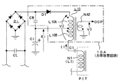
図1は、本発明を実施するための最良の形態(以下、実施の形態ともいう)として、第1の実施の形態のスイッチング電源回路の構成例を示した回路図である。この図に示す電源回路は、一次側の基本構成として、他励式によるハーフブリッジ結合方式による電流共振形コンバータに対して部分電圧共振回路が組み合わされた構成を採る。 FIG. 1 is a circuit diagram showing a configuration example of a switching power supply circuit according to a first embodiment as the best mode for carrying out the present invention (hereinafter also referred to as an embodiment). The power supply circuit shown in this figure employs a configuration in which a partial voltage resonance circuit is combined with a current resonance type converter using a half-bridge coupling method by a separate excitation type as a basic configuration on the primary side.
この図1に示す電源回路においては、先ず、商用交流電源ACに対し、フィルタコンデンサCL、CL、及びコモンモードチョークコイルCMCによるコモンモードノイズフィルタが形成されている。
そして、上記ノイズフィルタの後段となる商用交流電源ACに対しては、ブリッジ整流回路Di(整流回路部)及び1本の平滑コンデンサCiから成る全波整流平滑回路が接続される。この全波整流回路は、ブリッジ整流回路Diの正極入力端子に対して商用交流電源ACの正極ラインを接続し、ブリッジ整流回路Diの負極入力端子に対して商用交流電源ACの負極ラインを接続している。また、ブリッジ整流回路の正極出力端子と平滑コンデンサCiの正極端子とを接続している。そして、本実施の形態の場合には、ブリッジ整流回路の負極出力端子は、力率改善回路10を介するようにして平滑コンデンサCiの負極端子に対して接続される。
この場合、平滑コンデンサCiの負極端子は、一次側アースと接続されていることでアース電位(基準電位)となっている。つまり、この場合の力率改善回路10は、ブリッジ整流回路Diの負極出力ラインと基準電位との間に挿入される形態となる。
なお、力率改善回路10の構成及びその動作については後述する。
In the power supply circuit shown in FIG. 1, first, a common mode noise filter including filter capacitors CL and CL and a common mode choke coil CMC is formed for a commercial AC power supply AC.
A full-wave rectifying / smoothing circuit including a bridge rectifier circuit Di (rectifier circuit unit) and a single smoothing capacitor Ci is connected to the commercial AC power supply AC that is the subsequent stage of the noise filter. This full-wave rectifier circuit connects the positive line of the commercial AC power supply AC to the positive input terminal of the bridge rectifier circuit Di, and connects the negative line of the commercial AC power supply AC to the negative input terminal of the bridge rectifier circuit Di. ing. Further, the positive output terminal of the bridge rectifier circuit and the positive terminal of the smoothing capacitor Ci are connected. In the case of the present embodiment, the negative output terminal of the bridge rectifier circuit is connected to the negative terminal of the smoothing capacitor Ci via the power
In this case, the negative electrode terminal of the smoothing capacitor Ci has a ground potential (reference potential) by being connected to the primary side ground. That is, in this case, the power
The configuration and operation of the power
この全波整流平滑回路が商用交流電源ACを入力して全波整流動作を行うことによって、平滑コンデンサCiの両端にはブリッジ整流回路Diの整流出力を平滑化した整流平滑電圧Ei(直流入力電圧)が得られる。この場合の整流平滑電圧Eiは、交流入力電圧VACの等倍に対応したレベルとなる。また、この場合においては、ブリッジ整流回路Diを形成する4本の整流ダイオードには、低速リカバリ型を選定している。 The full-wave rectifying / smoothing circuit receives the commercial AC power supply AC and performs full-wave rectifying operation, so that the rectified and smoothed voltage Ei (DC input voltage) obtained by smoothing the rectified output of the bridge rectifying circuit Di is applied to both ends of the smoothing capacitor Ci. ) Is obtained. In this case, the rectified and smoothed voltage Ei is at a level corresponding to an equal magnification of the AC input voltage VAC. In this case, a low speed recovery type is selected for the four rectifier diodes forming the bridge rectifier circuit Di.
上記直流入力電圧を入力してスイッチング(断続)する電流共振形コンバータとしては、図示するようにして、MOS−FETによる2本のスイッチング素子Q1,Q2をハーフブリッジ結合により接続したスイッチング回路を備える。スイッチング素子Q1,Q2の各ドレイン−ソース間に対しては、ダンパーダイオードDD1,DD2が並列に接続される。ダンパーダイオードDD1のアノード、カソードは、それぞれスイッチング素子Q1のソース、ドレインと接続される。同様にして、ダンパーダイオードDD2のアノード、カソードは、それぞれスイッチング素子Q2のソース、ドレインと接続される。ダンパーダイオードDD1,DD2は、それぞれスイッチング素子Q1,Q2が備えるボディダイオードとされる。 As shown in the figure, the current resonance type converter for switching (intermittently) by inputting the DC input voltage includes a switching circuit in which two switching elements Q1 and Q2 by MOS-FETs are connected by half bridge coupling. Damper diodes DD1 and DD2 are connected in parallel between the drains and sources of the switching elements Q1 and Q2. The anode and cathode of the damper diode DD1 are connected to the source and drain of the switching element Q1, respectively. Similarly, the anode and cathode of the damper diode DD2 are connected to the source and drain of the switching element Q2, respectively. The damper diodes DD1 and DD2 are body diodes provided in the switching elements Q1 and Q2, respectively.
また、スイッチング素子Q2のドレイン−ソース間に対しては、部分共振コンデンサCpが並列に接続される。この部分共振コンデンサCpのキャパシタンスと一次巻線N1のリーケージインダクタンスL1によっては並列共振回路(部分電圧共振回路)を形成する。そして、スイッチング素子Q1,Q2のターンオフ時にのみ電圧共振する、部分電圧共振動作が得られるようになっている。 A partial resonance capacitor Cp is connected in parallel between the drain and source of the switching element Q2. A parallel resonance circuit (partial voltage resonance circuit) is formed by the capacitance of the partial resonance capacitor Cp and the leakage inductance L1 of the primary winding N1. A partial voltage resonance operation in which voltage resonance occurs only when the switching elements Q1, Q2 are turned off is obtained.
この電源回路においては、スイッチング素子Q1,Q2をスイッチング駆動するために、発振・ドライブ回路2が設けられる。この発振・ドライブ回路2は、発振回路、駆動回路を有しており、例えば汎用のICを用いることができる。そして、この発振・ドライブ回路2内の発振回路及び駆動回路によって、所要の周波数によるドライブ信号(ゲート電圧)をスイッチング素子Q1,Q2の各ゲートに対して印加する。これにより、スイッチング素子Q1,Q2は、所要のスイッチング周波数により交互にオン/オフするようにしてスイッチング動作を行う。
In this power supply circuit, an oscillation /
絶縁コンバータトランスPITは、スイッチング素子Q1 、Q2のスイッチング出力を二次側に伝送するために設けられる。
この絶縁トランスPITの一次巻線N1の一方の端部は、一次側直列共振コンデンサC1の直列接続を介して、力率改善回路10における高周波インダクタL10と、スイッチングダイオードD1のアノードとの接続点に対して接続される。また、一次巻線N1の他方の端部は、スイッチング素子Q1のソースとスイッチング素子Q2のドレインとの接続点(スイッチング出力点)に接続されることで、スイッチング出力が伝達されるようになっている。なお、スイッチングダイオードD1は、高速型として高速リカバリ型を選定する。
The insulating converter transformer PIT is provided to transmit the switching outputs of the switching elements Q1 and Q2 to the secondary side.
One end of the primary winding N1 of the insulation transformer PIT is connected to a connection point between the high-frequency inductor L10 in the power
ここで、絶縁コンバータトランスPITは、後述する構造により、絶縁コンバータトランスPITの一次巻線N1に所要のリーケージインダクタンスL1を生じさせる。そして、一次側直列共振コンデンサC1のキャパシタンスと、上記リーケージインダクタンスL1によっては一次側直列共振回路を形成する。上記した接続態様によればスイッチング素子Q1,Q2のスイッチング出力は、この一次側直列共振回路に伝達されることとなる。この一次側直列共振回路が、伝達されたスイッチング出力により共振動作を行うことで、一次側スイッチングコンバータの動作を電流共振形とする。 Here, the insulating converter transformer PIT generates a required leakage inductance L1 in the primary winding N1 of the insulating converter transformer PIT by a structure described later. A primary side series resonant circuit is formed by the capacitance of the primary side series resonant capacitor C1 and the leakage inductance L1. According to the connection mode described above, the switching outputs of the switching elements Q1, Q2 are transmitted to the primary side series resonance circuit. The primary side series resonance circuit performs a resonance operation by the transmitted switching output, thereby making the operation of the primary side switching converter a current resonance type.
上記説明によると、この図に示す一次側スイッチングコンバータとしては、一次側直列共振回路(L1−C1)による電流共振形としての動作と、前述した部分電圧共振回路(Cp//L1)とによる部分電圧共振動作とが得られることになる。
つまり、この図に示す電源回路は、一次側スイッチングコンバータを共振形とするための共振回路に対して、他の共振回路とが組み合わされた、複合共振形コンバータとしての構成を採っている。
According to the above description, the primary side switching converter shown in this figure has the operation as the current resonance type by the primary side series resonance circuit (L1-C1) and the part by the partial voltage resonance circuit (Cp // L1) described above. A voltage resonance operation is obtained.
That is, the power supply circuit shown in this figure has a configuration as a complex resonance type converter in which a resonance circuit for making the primary side switching converter a resonance type is combined with another resonance circuit.
絶縁コンバータトランスPITの二次巻線には一次巻線N1に伝達されたスイッチング出力に応じた交番電圧が励起される。そして、この場合の二次巻線N2としては、センタータップが施されたことで2つに分割された二次巻線N2A,N2Bが設けられる。この場合、二次巻線N2A,N2Bは同じ所定のターン数を有する。 An alternating voltage corresponding to the switching output transmitted to the primary winding N1 is excited in the secondary winding of the insulating converter transformer PIT. In this case, as the secondary winding N2, secondary windings N2A and N2B which are divided into two parts by providing a center tap are provided. In this case, the secondary windings N2A and N2B have the same predetermined number of turns.
そして、これら二次巻線N2A,N2Bに対しては、図示するように整流用素子としてNチャネルのMOS−FETQ3,Q4,Q5,Q6を備える、両波整流による同期整流回路が備えられる。
これらMOS−FETQ3〜Q6は、例えば低耐圧のトレンチ構造のものを選定することで、低オン抵抗を得るようにされる。
The secondary windings N2A and N2B are provided with a synchronous rectification circuit by double-wave rectification, which includes N-channel MOS-FETs Q3, Q4, Q5, and Q6 as rectification elements as shown in the figure.
For these MOS-FETs Q3 to Q6, for example, a low breakdown voltage trench structure is selected to obtain a low on-resistance.
絶縁コンバータトランスPITの二次巻線N2のセンタータップ出力は、図示するようにインダクタLdの直列接続を介して、平滑コンデンサCoの正極端子の接続点と接続される。 The center tap output of the secondary winding N2 of the insulating converter transformer PIT is connected to the connection point of the positive terminal of the smoothing capacitor Co through a series connection of the inductor Ld as shown.
そして、上記二次巻線N2の一方の端部(二次巻線N2B側の端部)は、MOS−FETQ3のドレインとMOS−FETQ5のドレインとの接続点に対して接続される。そして、これらMOS−FETQ3、Q5の各ソースの接続点が、二次側アースに接続される。
同様に、二次巻線N2の他方の端部(二次巻線N2A側の端部)は、MOS−FETQ4のドレインとMOS−FETQ6のドレインとの接続点に対して接続され、これらMOS−FETQ4、Q6の各ソースの接続点が二次側アースに接続されている。
なお、MOS−FETQ3,Q4,Q5,Q6のドレイン−ソースに対しては、それぞれ、ボディダイオードDD3,DD4,DD5,DD6が並列に接続される。
One end of the secondary winding N2 (the end on the secondary winding N2B side) is connected to a connection point between the drain of the MOS-FET Q3 and the drain of the MOS-FET Q5. The connection points of the sources of these MOS-FETs Q3 and Q5 are connected to the secondary side ground.
Similarly, the other end of the secondary winding N2 (the end on the secondary winding N2A side) is connected to a connection point between the drain of the MOS-FET Q4 and the drain of the MOS-FET Q6. The connection point of the sources of the FETs Q4 and Q6 is connected to the secondary side ground.
Body diodes DD3, DD4, DD5, DD6 are connected in parallel to the drain-sources of the MOS-FETs Q3, Q4, Q5, Q6, respectively.
このような接続形態によれば、二次巻線N2Bを含む整流電流経路においては、整流素子であるMOS−FETQ3//MOS−FETQ5の並列接続回路が直列に挿入されることになる。また、二次巻線N2Aを含む整流電流経路においては、同じく整流素子であるMOS−FETQ4//MOS−FETQ6の並列接続回路が直列に挿入された構成となっている。 According to such a connection form, in the rectification current path including the secondary winding N2B, the parallel connection circuit of the MOS-FET Q3 // MOS-FET Q5 which is the rectification element is inserted in series. In the rectified current path including the secondary winding N2A, a parallel connection circuit of MOS-FET Q4 // MOS-FET Q6, which is also a rectifying element, is inserted in series.
また、この図に示される同期整流回路において、MOS−FETQ3とMOS−FETQ5を駆動する駆動回路は、二次巻線N2Aのセンタータップしていない側の端部とMOS−FETQ3、Q5のゲートとの間に共通に挿入されるようにして、ゲート抵抗Rg1を接続して形成される。
同様に、MOS−FETQ4、Q6を駆動する駆動回路は、二次巻線N2Bのセンタータップしていない端部とMOS−FETQ4、Q6のゲートとの間に共通となるようにして挿入された、ゲート抵抗Rg2を備えて形成される。
つまりこの場合、上記MOS−FETQ3,Q5は、上記二次巻線N2Aに励起される交番電圧が上記ゲート抵抗Rg1により検出されることで、同じタイミングでオン(導通)/オフ(非導通)するようにされ、MOS−FETQ4,Q6も、二次巻線N2Bに励起される交番電圧が上記ゲート抵抗Rg2により検出されることで、同じタイミングでオン(導通)/オフ(非導通)するようにされているものである。
また、MOS−FETQ3,Q5の組が、二次巻線N2Aのセンタータップされていない端部の電圧に応じてオン/オフし、MOS−FETQ4,Q6の組が二次巻線N2Bのセンタータップされていない端部の電圧に応じてオン/オフするということは、互いのMOS−FETの組が、逆極性となる交番電圧に応じてオン/オフするということになる。つまり、MOS−FETQ3,Q5の組と、MOS−FETQ4,Q6の組とでは、二次巻線N2に励起される交番電圧が反転するタイミングに応じて、交互にオン/オフするようにして整流動作(スイッチング動作)を行う。
In the synchronous rectifier circuit shown in this figure, the drive circuit for driving the MOS-FET Q3 and the MOS-FET Q5 includes the end of the secondary winding N2A on the side not center-tapped and the gates of the MOS-FETs Q3 and Q5. The gate resistor Rg1 is connected so as to be inserted in common.
Similarly, the driving circuit for driving the MOS-FETs Q4 and Q6 is inserted so as to be common between the end portion of the secondary winding N2B which is not center-tapped and the gates of the MOS-FETs Q4 and Q6. It is formed with a gate resistance Rg2.
That is, in this case, the MOS-FETs Q3 and Q5 are turned on (conducting) / off (non-conducting) at the same timing when the alternating voltage excited by the secondary winding N2A is detected by the gate resistor Rg1. The MOS-FETs Q4 and Q6 are also turned on (conducting) / off (nonconducting) at the same timing when the alternating voltage excited by the secondary winding N2B is detected by the gate resistance Rg2. It is what has been.
Also, the pair of MOS-FETs Q3 and Q5 is turned on / off according to the voltage at the end of the secondary winding N2A that is not center-tapped, and the pair of MOS-FETs Q4 and Q6 is the center tap of the secondary winding N2B. Turning on / off according to the voltage at the end that is not performed means that each pair of MOS-FETs is turned on / off according to an alternating voltage having a reverse polarity. That is, the MOS-FETs Q3 and Q5 and the MOS-FETs Q4 and Q6 are rectified so that they are alternately turned on / off according to the timing at which the alternating voltage excited by the secondary winding N2 is inverted. The operation (switching operation) is performed.
ここで、MOS−FETは、ゲートにオン電圧を印加すると、ドレイン−ソース間は単なる抵抗体と等価となるので、電流は双方向に流れる。これを二次側の整流素子として機能させようとすれば、二次側平滑コンデンサ(平滑コンデンサCo1〜Co4)の正極端子に充電する方向のみに電流を流さなければならない。これとは逆方向に電流が流れると、二次側平滑コンデンサから絶縁コンバータトランスPIT側に放電電流が流れて、負荷側に有効に電力を伝達することができなくなる。また、逆電流によるMOS−FETの発熱、ノイズなどが生じて、一次側におけるスイッチング損失も招く。
上記した駆動回路は、二次巻線の電圧を検出することに基づいて、二次側平滑コンデンサの正極端子に充電する方向(つまり、この場合ではソース→ドレイン方向)の電流のみが流れるように、MOS−FETQ3〜Q6をスイッチング駆動するための回路である。つまり、この場合における同期整流回路の回路構成としては、巻線電圧検出方式により、整流電流に同期させてMOS−FETをオン/オフ駆動する構成を採っているものである。
Here, when an ON voltage is applied to the gate of the MOS-FET, the drain-source is equivalent to a mere resistor, so that current flows in both directions. If this is to function as a secondary side rectifying element, it is necessary to pass a current only in the direction in which the positive terminals of the secondary side smoothing capacitors (smoothing capacitors Co1 to Co4) are charged. If a current flows in the opposite direction, a discharge current flows from the secondary side smoothing capacitor to the insulating converter transformer PIT side, and power cannot be effectively transmitted to the load side. Further, the MOS-FET generates heat and noise due to the reverse current, resulting in switching loss on the primary side.
Based on the detection of the voltage of the secondary winding, the drive circuit described above is such that only the current in the direction of charging the positive terminal of the secondary-side smoothing capacitor (that is, in this case, the source-to-drain direction) flows. This is a circuit for switching the MOS-FETs Q3 to Q6. In other words, the circuit configuration of the synchronous rectifier circuit in this case employs a configuration in which the MOS-FET is driven on / off in synchronization with the rectified current by the winding voltage detection method.
なお、この場合、MOS−FETQ3,Q5の組の駆動回路系を形成するとされるゲート抵抗Rg1と、MOS−FETQ4,Q6の組の駆動回路系を形成するとされるゲート抵抗Rg2に対しては、それぞれ並列にショットキーダイオードDg1、ショットキーダイオードDg2を図示する方向により接続するようにしている。このようにしてショットキーダイオードDg1,Dg2を挿入することによっては、それぞれMOS−FETQ3,Q5,Q4,Q6のゲート入力容量の蓄積電荷を、これらのターンオフ時に対応して、ショットキーダイオードDg1、ショットキーダイオードDg2を経由して放電するための経路が形成される。そして、これによってこれらMOS−FETを確実にターンオフさせて、良好なスイッチング特性を得るようにしているものである。 In this case, for the gate resistor Rg1 that is to form the drive circuit system of the MOS-FETs Q3 and Q5 and the gate resistor Rg2 that is to form the drive circuit system of the MOS-FETs Q4 and Q6, A Schottky diode Dg1 and a Schottky diode Dg2 are connected in parallel in the direction shown in the figure. By inserting the Schottky diodes Dg1 and Dg2 in this way, the accumulated charges of the gate input capacitances of the MOS-FETs Q3, Q5, Q4, and Q6 correspond to the Schottky diodes Dg1 and Schottky corresponding to these turn-off times, respectively. A path for discharging via the key diode Dg2 is formed. As a result, these MOS-FETs are reliably turned off to obtain good switching characteristics.
また、上述もしたように、この図1に示す電源回路では、二次巻線N2のセンタータップと二次側平滑コンデンサとの間に、インダクタLdを直列に挿入している。すなわちこの場合、インダクタLdを、二次側の整流電流経路において二次側交番電圧が正/負の各期間で共通に整流電流が流れるラインに対して挿入しているものである。
このようにしてインダクタLdを挿入することによっては、二次側直流出力電圧Eoに発生するとされていたノイズの抑制を図ることができる。
二次側の整流回路として、MOS−FETによる同期整流回路を備えた場合、これらMOS−FETによるスイッチングノイズ等の影響により二次側直流出力電圧Eoには高周波ノイズが重畳し易くなる。そこで、このように整流電流経路に対してインダクタLdを挿入することで、高周波のノイズ成分について、そのインピーダンス成分によって平滑化することで抑制するようにしている。
また、このように整流電流経路に挿入されたインダクタLdによっては二次側整流電流に生じるとされる逆方向電流の発生を抑制するようにもされる。
Further, as described above, in the power supply circuit shown in FIG. 1, the inductor Ld is inserted in series between the center tap of the secondary winding N2 and the secondary side smoothing capacitor. That is, in this case, the inductor Ld is inserted into the line through which the rectified current flows in common in each period in which the secondary-side alternating voltage is positive / negative in the secondary-side rectified current path.
By inserting the inductor Ld in this way, it is possible to suppress noise that was supposed to be generated in the secondary side DC output voltage Eo.
When a secondary rectifier circuit is provided with a synchronous rectifier circuit using a MOS-FET, high-frequency noise is easily superimposed on the secondary-side DC output voltage Eo due to the influence of switching noise or the like caused by the MOS-FET. Thus, by inserting the inductor Ld into the rectified current path in this way, the high frequency noise component is suppressed by smoothing with the impedance component.
In addition, the inductor Ld inserted in the rectified current path in this way suppresses the generation of reverse current that is supposed to occur in the secondary side rectified current.
これまでに説明した回路構成による同期整流回路によっては、二次側平滑コンデンサに対して両波整流により整流して得られる整流電流を充電する動作が得られる。
すなわち、二次側に励起される交番電圧の一方の半周期には、二次巻線N2Bから流れる電流が、MOS−FETQ3//Q5の並列接続回路をソース→ドレイン方向に導通し、平滑コンデンサCoに対して充電される。また、交番電圧の他方の半周期には、二次巻線N2Aに流れる電流がMOS−FETQ3//Q5の並列接続回路をソース→ドレイン方向に導通し、平滑コンデンサCoに対して充電される。これによって、上記交番電圧が正/負の期間で平滑コンデンサCoに充電する両波整流動作が得られるものである。
そして、このような平滑コンデンサの両端電圧として、図のような二次側直流出力電圧Eoが得られる。この二次側直流出力電圧Eoは、図示しない負荷側に供給されるとともに、次に説明する制御回路1のための検出電圧としても分岐して入力される。
With the synchronous rectifier circuit having the circuit configuration described so far, an operation of charging a rectified current obtained by rectifying the secondary-side smoothing capacitor by double-wave rectification can be obtained.
That is, in one half cycle of the alternating voltage excited on the secondary side, the current flowing from the secondary winding N2B conducts through the parallel connection circuit of the MOS-FET Q3 // Q5 in the source-to-drain direction, and the smoothing capacitor Charged to Co. In the other half cycle of the alternating voltage, the current flowing through the secondary winding N2A is conducted in the source-to-drain direction through the parallel connection circuit of the MOS-FET Q3 // Q5, and the smoothing capacitor Co is charged. As a result, a double-wave rectification operation in which the smoothing capacitor Co is charged in a period in which the alternating voltage is positive / negative can be obtained.
A secondary side DC output voltage Eo as shown in the figure is obtained as the voltage across the smoothing capacitor. The secondary side DC output voltage Eo is supplied to a load side (not shown) and is also branched and input as a detection voltage for the
なお、本実施の形態において、同期整流回路について、上記のようにして、整流素子としてのMOS−FETを並列に接続しているのは、次のような理由による。
ここでの例として、本実施の形態の電源回路が実際に対応すべき負荷条件としては、二次側直流出力電圧Eo=5Vに対して、負荷電流が30A〜0Aで変動するものとしている。これは、いわゆる低電圧/大電流といわれる、実質的には相当に変動幅が広範囲となる負荷条件であり、従って、負荷が重くなる傾向では、二次側整流回路にも相当に大きな電流が流れる。そこで、整流素子であるMOS−FETについて、複数本を並列接続した構成とすることで、大電流が流れるときの素子への負担を軽減して、高い信頼性を確保することとしているものである。
In the present embodiment, the MOS-FETs as the rectifier elements are connected in parallel in the synchronous rectifier circuit as described above for the following reason.
As an example here, as a load condition that the power supply circuit of the present embodiment should actually cope with, the load current varies from 30 A to 0 A with respect to the secondary side DC output voltage Eo = 5V. This is a so-called low voltage / large current load condition in which the fluctuation range is substantially wide. Therefore, if the load tends to be heavy, a considerably large current is also applied to the secondary side rectifier circuit. Flowing. Therefore, the MOS-FET that is a rectifier element is configured to have a plurality of parallel connections, thereby reducing the burden on the element when a large current flows and ensuring high reliability. .
制御回路1は、二次側直流出力電圧Eoのレベル変化に応じた検出出力を発振・ドライブ回路2に供給する。発振・ドライブ回路2では、入力された制御回路1の検出出力に応じてスイッチング周波数が可変されるようにして、スイッチング素子Q1,Q2を駆動する。スイッチング素子Q1,Q2のスイッチング周波数が可変されることで、一次側直列共振回路の共振インピーダンスが変化し、絶縁コンバータトランスPITの一次巻線N1から二次巻線N2(N2A,N2B)側に伝送される電力量も変化するが、これにより二次側直流出力電圧Eoのレベルを安定化させるように動作する。
例えば重負荷の傾向となって二次側直流出力電圧Eoが低下するのに応じては、上記スイッチング周波数を低くするように制御するが、これは共振インピーダンスを小さくすることとなり、このために二次側直流出力電圧Eoを上昇させる。これに対して、軽負荷の傾向となって二次側直流出力電圧Eoが上昇するのに応じては、上記スイッチング周波数を高くするように制御することで、共振インピーダンスを大きくし、二次側直流出力電圧Eoを低下させる。
The
For example, when the secondary-side DC output voltage Eo decreases due to a heavy load tendency, the switching frequency is controlled to be lowered. However, this reduces the resonant impedance. The secondary side DC output voltage Eo is raised. On the other hand, when the secondary side DC output voltage Eo rises due to a light load tendency, the resonance impedance is increased by controlling the switching frequency to be increased, and the secondary side The DC output voltage Eo is reduced.
続いて、力率改善回路10の構成について説明する。
前述もしたように、この力率改善回路10は、商用交流電源ACから直流入力電圧(Ei)を得るための整流平滑回路における整流電流経路に対して挿入されるようにして設けられるもので、電力回生方式として磁気結合形による力率改善回路の構成を採る。
Next, the configuration of the power
As described above, the power
力率改善回路10においては、先ず、ブリッジ整流回路Diの負極出力端子に対して、高速リカバリ型であるスイッチングダイオード(力率改善用スイッチング素子)D1のカソードが接続される。スイッチングダイオードD1のアノードは、高周波インダクタL10の巻始め端部と接続され、高周波インダクタL10の巻終わり端部は一次側アースに接続される。
これにより、力率改善回路10においては、スイッチングダイオードD1−高周波インダクタL10による直列接続回路が形成され、この直列接続回路がブリッジ整流回路Diの負極出力端子と一次側アース間に挿入されるものとなる。
In the power
Thereby, in the power
ただし、本実施の形態においては、過電流保護機能に対応して負荷電流検出を行なうためのものとして、力率改善回路内に、電流検出巻線NADを設けることとしている。この電流検出巻線NADは、高周波インダクタL10に対して磁気結合されるようにようにして巻装される。また、電流検出巻線NADと高周波インダクタL10は密結合するようにして巻装する。つまり、高周波インダクタl10としてのコイル部品は、一次側に対して本来の高周波インダクタL10としての巻線を巻装し、二次側に対しては、この一次側の巻線と密結合となるようにして電流検出巻線NADを巻装した構造を有する。なお、この場合における電流検出巻線NADの巻数(ターン数)としては1T(ターン)でよいものとされる。また、一次側の高周波インダクタL10の巻線と、電流検出巻線NADの巻方向(極性)は相互に同じとなるようにしている。 However, in the present embodiment, the current detection winding NAD is provided in the power factor correction circuit as a load current detection corresponding to the overcurrent protection function. The current detection winding NAD is wound so as to be magnetically coupled to the high frequency inductor L10. The current detection winding NAD and the high frequency inductor L10 are wound so as to be tightly coupled. That is, the coil component as the high-frequency inductor l10 is wound with the original winding as the high-frequency inductor L10 on the primary side, and is tightly coupled with the primary-side winding on the secondary side. Thus, the current detection winding NAD is wound. In this case, the number of turns (number of turns) of the current detection winding NAD may be 1T (turns). Further, the winding direction (polarity) of the primary side high-frequency inductor L10 and the current detection winding NAD are made the same.
この場合、電流検出巻線NADの巻始め端部側を発振・ドライブ回路2の過電流保護用端子(OCP端子)に接続し、巻終わり端部を一次側アース(基準電位)に接続している。これにより、発振・ドライブ回路2の過電流保護用端子(OCP端子)に対しては、電流検出巻線NADの両端電圧(検出電圧)V3が入力されることになる。電流検出巻線NADの端部が一次側アースに接地されていることで、この検出電圧V3は、基準電位(アース電位)に対する電位差として得られる。発振・ドライブ回路2は、このようにして入力される検出電圧V3のレベル値に基づいて、後述するようにして過電流検出を行う。
In this case, the winding start end side of the current detection winding NAD is connected to the overcurrent protection terminal (OCP terminal) of the oscillation /
フィルタコンデンサCNは、スイッチングダイオードD1のスイッチング動作により生じるスイッチング周期の交番成分を吸収することでノーマルモードノイズを抑制するために設けられるもので、図示するようにして、スイッチングダイオードD1−高周波インダクタL10の直列接続回路に対して並列に接続される。
そして、一次側直列共振回路(L1−C1)の端部を、スイッチングダイオードD1のアノードと高周波インダクタL10との接続点に対して接続するようにされる。
The filter capacitor CN is provided to suppress the normal mode noise by absorbing the alternating component of the switching period generated by the switching operation of the switching diode D1, and as shown in the figure, the switching diode D1−the high frequency inductor L10. Connected in parallel to the series connection circuit.
The end of the primary side series resonant circuit (L1-C1) is connected to the connection point between the anode of the switching diode D1 and the high frequency inductor L10.
このような力率改善回路10の回路構成では、一次側直列共振回路に得られるスイッチング出力(一次側直列共振電流I1)を電力として回生して、高周波インダクタL10の磁気結合を介するようにして平滑コンデンサCiに帰還する動作が得られているということがいえる。
In such a circuit configuration of the power
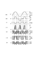
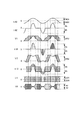
図3の波形図は、力率改善回路10による力率改善動作を、商用交流電源周期により示している。なお、この図に示す特性は、交流入力電圧VAC=230Vで、負荷電力Po=150Wの最大負荷電力の条件のもとで得られたものである。
The waveform diagram of FIG. 3 shows the power factor correction operation by the power
ここで、図示するようにして50Hzで325Vpの交流入力電圧VACが入力されていることを前提として、上記のようにして力率改善回路10側に対して、一次側直列共振回路から電力回生が行われているものとする。
これに応じて、高周波インダクタL10の両端電圧V2は、スイッチング周期による交番電圧として、図示するようにして、+100Vと−200Vの範囲でエンベロープが変化する波形が得られることになる。高速リカバリ型のスイッチングダイオードD1には、この電圧V2が印加されることになる。そして、電圧V2が負極性方向で略凹字状のエンベロープとなって負極性の絶対値レベルが一定以上となっている期間において、この電圧V2によりスイッチングダイオードD1をオン/オフさせる動作が得られる。これにより、例えば交流入力電圧VACの正/負の絶対値が、そのピーク値の約1/2以上のときにもスイッチングダイオードD1がスイッチング動作を行い、電流検出巻線NAD−高周波インダクタL10を介して平滑コンデンサCiからブリッジ整流回路Diの負極出力端子に流入しようとする整流電流を断続するようにされる。
このときにスイッチングダイオードD1に流れる整流電流I11は、図示するようにして、正極性による略正弦波の半波のエンベロープを有する、スイッチング周期による交番電流となる。この場合において、交流入力電圧VACがピークとなる時点に対応する整流電流I11のレベルは、4Aとなる。
Here, assuming that an AC input voltage VAC of 325 Vp is input at 50 Hz as shown in the figure, power regeneration from the primary side series resonance circuit is performed on the power
Correspondingly, the voltage V2 across the high-frequency inductor L10 is obtained as an alternating voltage depending on the switching period, and as shown in the figure, a waveform whose envelope changes in the range of + 100V and -200V is obtained. The voltage V2 is applied to the fast recovery switching diode D1. Then, during the period in which the voltage V2 becomes a substantially concave envelope in the negative polarity direction and the absolute value level of the negative polarity is equal to or higher than a certain level, an operation of turning on / off the switching diode D1 by the voltage V2 is obtained. . As a result, for example, when the positive / negative absolute value of the AC input voltage VAC is about ½ or more of the peak value, the switching diode D1 performs the switching operation, and the current detection winding NAD−the high frequency inductor L10. Thus, the rectified current that is about to flow from the smoothing capacitor Ci to the negative output terminal of the bridge rectifier circuit Di is interrupted.
At this time, the rectified current I11 flowing through the switching diode D1 is an alternating current having a switching cycle having a substantially sinusoidal half-wave envelope with positive polarity as shown in the figure. In this case, the level of the rectified current I11 corresponding to the time when the AC input voltage VAC reaches a peak is 4A.
また、高周波インダクタL10に流れる電流I12は、例えば±2.2Aの振幅範囲において、図示するようにしてエンベロープが変化する交番波形となる。本実施の形態の場合、一次側直列共振電流I1は、整流電流I11の交番周期成分と、この電流I12の成分とで分岐して流れることになる。
また、フィルタコンデンサCNの両端電圧V1は、電圧V2の正極性のエンベロープを有する波形となる。
Further, the current I12 flowing through the high-frequency inductor L10 has an alternating waveform whose envelope changes as shown in the amplitude range of ± 2.2 A, for example. In the case of the present embodiment, the primary side series resonance current I1 branches and flows between an alternating period component of the rectified current I11 and a component of this current I12.
The voltage V1 across the filter capacitor CN has a waveform having a positive envelope of the voltage V2.
上記のようにしてスイッチングダイオードD1が整流電流を断続するようにしてスイッチングすることで得られる整流電流I11の導通期間は、ブリッジ整流回路Diから出力される整流出力電圧レベルが平滑コンデンサCiの両端電圧よりも低いとされる期間にも流れるものとなっており、同じ図3に示す交流入力電流IACの導通期間も、この整流出力電流I1の導通期間にほぼ一致したものとなる。つまり、交流入力電流IACの導通角は、力率改善回路を備えない場合よりも拡大されているものであり、交流入力電流IACの波形としては、交流入力電圧VACの波形に近付くものとなっている。つまり、力率改善が図られていることになる。なお、交流入力電流IACのピークレベルは、この場合2Aとなっている。 In the conduction period of the rectified current I11 obtained by switching the switching diode D1 so that the rectified current is interrupted as described above, the rectified output voltage level output from the bridge rectifier circuit Di is the voltage across the smoothing capacitor Ci. The conduction period of the AC input current IAC shown in FIG. 3 also substantially coincides with the conduction period of the rectified output current I1. That is, the conduction angle of the AC input current IAC is larger than that without the power factor correction circuit, and the waveform of the AC input current IAC approaches the waveform of the AC input voltage VAC. Yes. That is, the power factor is improved. In this case, the peak level of the AC input current IAC is 2A.
また、電流検出巻線NADは、高周波インダクタL10の巻線と密結合の状態で磁気結合していることで、電流検出巻線NADには、高周波インダクタL10の両端電圧である電圧V2に応じた交番電圧が誘起されるが、この交番電圧(電流検出巻線NADの両端電圧)が、検出電圧V3となる。この検出電圧V3は、図示するようにして、電圧V2と相似したもので、±4Vの範囲で振幅する波形となる。
ここで、高周波インダクタL10に流れる電流I12は、上記もしているように、一次側直列共振電流I1の成分が分岐して流れるものであり、従って、一次側直列共振電流I1に対応したレベルを有する。そして、この電流I12が流れるのに応じて高周波インダクタL10の両端に発生する得られる電圧V2も、電流I12に応じたレベルを有することになる。このことから、電圧V2によって誘起される検出電圧V3としても一次側直列共振電流I1に対応するレベルが得られるものとなることが分かる。
そして、最大負荷電力時における一次側直列共振電流I1のレベルに応じて、検出電圧V3としては、上記のようにして±4Vの振幅が得られている。この振幅レベルは、特に増幅を行わなくとも、発振・ドライブ回路2が適正に過電流検出を行うのには充分なレベルとされる。
なお、先にも述べたように、電流検出巻線NADの巻数は1Tである。また、高周波インダクタL10のインダクタとしては92μHを設定している。
Further, since the current detection winding NAD is magnetically coupled with the winding of the high frequency inductor L10 in a tightly coupled state, the current detection winding NAD has a voltage V2 corresponding to the voltage across the high frequency inductor L10. An alternating voltage is induced, and this alternating voltage (the voltage across the current detection winding NAD) becomes the detection voltage V3. This detection voltage V3 is similar to the voltage V2 as shown in the figure, and has a waveform with an amplitude in the range of ± 4V.
Here, as described above, the current I12 flowing through the high-frequency inductor L10 is one in which the component of the primary side series resonance current I1 branches and flows, and thus has a level corresponding to the primary side series resonance current I1. . The voltage V2 obtained at both ends of the high frequency inductor L10 in response to the current I12 flowing also has a level corresponding to the current I12. From this, it is understood that a level corresponding to the primary side series resonance current I1 can be obtained as the detection voltage V3 induced by the voltage V2.
Then, according to the level of the primary side series resonance current I1 at the maximum load power, the detection voltage V3 has an amplitude of ± 4 V as described above. This amplitude level is set to a level sufficient for the oscillation /
As described above, the number of turns of the current detection winding NAD is 1T. Further, 92 μH is set as the inductor of the high frequency inductor L10.
ここで、本実施の形態における過電流保護動作についても説明しておく。
上記のようにして、発振・ドライブ回路2は、OCP端子に入力される検出電圧V3(電流検出巻線NADの両端電圧)のレベルについて、負荷電流が過電流とされる状態に対応する所定以上となるか否かについての判定を行うようにされる。例えば本実施の形態としても、最大負荷電力Po=150Wをオーバーして、負荷電力Poが175W以上になった状態を過電流の状態とみなすこととしている。
また、確認のために述べておくと、上記説明から理解されるように、電流検出巻線NADの両端電圧(検出電圧V3)として得られるのは、一次側直列共振電流I1に対応するレベルであり、一次側直列共振電流I1のレベルは、負荷電流レベルに対応するものとなる。従って、検出電圧V3は、二次側直流出力電圧Eoの負荷に流れる負荷電流のレベル(電流量)を示していることになる。また、電流検出巻線NADの一端は一次側アース(基準電位)に対して接続されており、従って、その両端電圧(検出電圧V3)としても、この基準電位に対する電位差を有している。発振・ドライブ回路2もアース電位を基準電位として動作しているから、検出電圧V3により、適正にレベル検出が行えることが理解される。
Here, the overcurrent protection operation in the present embodiment will also be described.
As described above, the oscillation /
For confirmation, as understood from the above description, the voltage across the current detection winding NAD (detection voltage V3) is obtained at a level corresponding to the primary series resonance current I1. Yes, the level of the primary side series resonance current I1 corresponds to the load current level. Therefore, the detection voltage V3 indicates the level (current amount) of the load current flowing through the load of the secondary side DC output voltage Eo. Further, one end of the current detection winding NAD is connected to the primary side ground (reference potential), and therefore the voltage across the end (detection voltage V3) has a potential difference with respect to this reference potential. Since the oscillation /
そして、発振・ドライブ回路2は、過電流保護動作として、検出電圧V3が所定レベル以上になったことを判定すると、内部の発振回路の発振動作を停止させる。これにより、スイッチング素子Q1,Q2を駆動するためのドライブ信号としても周期的なものではなくなるために、スイッチング素子Q1,Q2についてのスイッチング動作が停止されることになる。これにより、過電流に対する保護が図られることとなる。なお、このようなスイッチング動作の停止に応じた動作としては、先に図11に示した特性と同様となる。つまり、二次側直流出力電圧Eoはフの字特性となり、力率PF、及びスイッチング周波数fsは、垂下する特性となる。
The oscillation /
また、先に図3によっても説明したように、電流検出巻線NADにて得られる検出レベルは、最大負荷電力時においても4Vという高いレベルである。つまり、本実施の形態としては、増幅を必要としない程度に充分な検出電圧V3のレベルが得られている。これにより、増幅回路(検出回路3)を追加する必要はないこととなる。
また、一次側にて電流検出を行うようにしたことによっては、検出出力を二次側から一次側の発振・ドライブ回路に伝達する必要はない。このために、フォトカプラなどに代表される、直流的絶縁を行って検出出力の伝送を行なうための部品素子も必要ないこととなる。
Further, as described above with reference to FIG. 3, the detection level obtained by the current detection winding NAD is a high level of 4 V even at the maximum load power. That is, in the present embodiment, a level of the detection voltage V3 sufficient to avoid the need for amplification is obtained. Thereby, it is not necessary to add an amplifier circuit (detection circuit 3).
Further, since current detection is performed on the primary side, it is not necessary to transmit the detection output from the secondary side to the oscillation / drive circuit on the primary side. For this reason, there is no need for a component element for transmitting detection output by performing DC insulation, such as a photocoupler.
また、先の図10のようにして二次側にて過電流検出を行う場合、負荷電流に応じて流れる二次側整流電流のレベルが比較的大きいことから、電流検出抵抗R1A//R1Bによる電力損失としては比較的大きなものとなっていた。特に、図10に示した電源回路は、二次側直流出力電圧Eo=5V、負荷電流0〜30Aとされる定電圧/大電流の負荷条件なので、この問題が特に顕著であり、例えば、最大負荷電力Po=150W時においては、4.5Wの電力損失が生じていたものである。
これに対して、本実施の形態では、図3にも示したように、電流検出素子としては、1Tの電流検出巻線NADであり、この両端電圧である検出電圧V3は、高周波インダクタL10により誘起される電圧である。従って、電流検出巻線NADにおける電力損失は0であるということがいえる。
Further, when overcurrent detection is performed on the secondary side as shown in FIG. 10 above, the level of the secondary side rectified current flowing according to the load current is relatively large, so that the current detection resistor R1A // R1B The power loss was relatively large. In particular, since the power supply circuit shown in FIG. 10 has a constant voltage / large current load condition where the secondary side DC output voltage Eo = 5 V and the load current is 0 to 30 A, this problem is particularly remarkable. When the load power Po = 150 W, a power loss of 4.5 W occurred.
On the other hand, in the present embodiment, as shown in FIG. 3, the current detection element is a 1T current detection winding NAD, and the detection voltage V3, which is the voltage at both ends, is obtained by the high frequency inductor L10. This is the induced voltage. Therefore, it can be said that the power loss in the current detection winding NAD is zero.
このようにして、本実施の形態においては、電力回生方式による力率改善の構成を採りながらも、高周波インダクタL10に対して電流検出巻線NADを密結合させて巻装して、この電流検出巻線NADに誘起される両端電圧を検出電圧V3として利用することで、一次側直列共振電流レベル(つまり負荷電流レベル)について、一次側のアース電位を基準に検出することが可能とされる。
このような本実施の形態の構成は、高周波インダクタL10を一次側とし、電流検出巻線NADを二次巻線とする構成は、カレントトランスとして機能しているものであると捉えることができる。つまり、本実施の形態では、電力回生方式の力率改善回路として必須的に備えられる高周波インダクタを、カレントトランスの一次側巻線としても機能させることとしているということがいえる。
この結果、上記しているように、増幅回路及びフォトカプラなどの直流分絶縁用部品が省略されることになって、例えば電源回路基板の小型軽量化及び低コスト化を図ることができる。また、電流検出部品である電流検出巻線NADにおける電力損失は0とされることで、電源回路全体としてみた場合のAC→DC電力変換効率の向上も図られることとなる。
In this way, in the present embodiment, while adopting the power factor improvement configuration by the power regeneration method, the current detection winding NAD is tightly coupled and wound around the high frequency inductor L10, and this current detection is performed. By using the both-end voltage induced in the winding NAD as the detection voltage V3, the primary side series resonance current level (that is, the load current level) can be detected with reference to the primary side ground potential.
Such a configuration of the present embodiment can be regarded as a configuration in which the high-frequency inductor L10 is the primary side and the current detection winding NAD is the secondary winding functions as a current transformer. That is, in this embodiment, it can be said that the high-frequency inductor that is essentially provided as a power regeneration type power factor correction circuit also functions as the primary winding of the current transformer.
As a result, as described above, components for direct current insulation such as an amplifier circuit and a photocoupler are omitted, and for example, the power circuit board can be reduced in size and weight and cost can be reduced. In addition, since the power loss in the current detection winding NAD that is a current detection component is set to 0, the AC → DC power conversion efficiency in the case of the entire power supply circuit can be improved.
ところで、先に図10に示した電源回路におけるようなスイッチングコンバータの構成では、一次側のスイッチング素子のスイッチング周波数の可変制御により、二次側直流出力電圧の安定化を図るようにされている。このような構成を採る場合において、例えば軽負荷の傾向となっている状態では、スイッチング周波数を高くするように制御して安定化を図ることになる。この状態では、二次側の整流回路において、二次側整流電流が二次側平滑コンデンサに流れる期間が連続し、休止する期間が存在しない、いわゆる連続モードの動作となる。
これに対して、重負荷の傾向となって二次側直流出力電圧が低下するのに応じて一次側のスイッチング周波数を低くするように制御していくと、二次側平滑コンデンサに対して二次側整流電流が連続して流れなくなって電流不連続期間が生じる、いわゆる不連続モードに移行する。つまり、二次側の両波整流動作として、負荷変動に応じて不連続モードとなる状態が存在する。
なお、二次側直流出力電圧は、商用交流電源AC(交流入力電圧VAC)に応じても変動し、これに応じた定電圧制御動作も行われるから、交流入力電圧VACのレベルに応じても不連続モードとなる状態が存在することになる。
By the way, in the configuration of the switching converter as in the power supply circuit shown in FIG. 10, the secondary side DC output voltage is stabilized by variable control of the switching frequency of the primary side switching element. In the case of adopting such a configuration, for example, in a state where the load tends to be light, stabilization is achieved by controlling the switching frequency to be high. In this state, the secondary-side rectifier circuit operates in a so-called continuous mode in which the period during which the secondary-side rectified current flows through the secondary-side smoothing capacitor is continuous and there is no period of pause.
On the other hand, if the primary side switching frequency is controlled to decrease as the secondary side DC output voltage decreases due to a heavy load tendency, the secondary side smoothing capacitor will The so-called discontinuous mode is entered, in which the secondary side rectified current stops flowing continuously and a current discontinuous period occurs. That is, there is a state in which the discontinuous mode is set according to the load variation as the secondary-side double-wave rectification operation.
The secondary side DC output voltage varies depending on the commercial AC power supply AC (AC input voltage VAC), and a constant voltage control operation corresponding to this is also performed, so that the secondary side DC output voltage also depends on the level of the AC input voltage VAC. There will be a state of discontinuous mode.
図10に示した電源回路のようにして、電力回生方式により力率改善を行う構成では、一次側直列共振電流に商用交流電源周期のリップルが重畳することにより、二次側直流出力電圧に重畳される商用交流電源周期のリップル電圧が、力率改善回路を備えない構成とした場合よりも大幅に増加する。
これは、上記のようにして、例えば負荷変動、交流入力電圧VACの変動により、二次側整流動作が不連続モードとなることが主たる原因となっている。このことは、換言すれば、負荷変動、交流入力電圧VACの変動にかかわらず、二次側整流動作として連続モードが維持されるようにすれば、その原因が無くなるのであるから、上記した二次側直流出力電圧に重畳する商用交流電源周期のリップル電圧の増加を有効に抑制できるということを意味する。
In the configuration in which the power factor is improved by the power regeneration method like the power supply circuit shown in FIG. 10, the ripple on the commercial AC power supply cycle is superimposed on the primary side series resonance current so that it is superimposed on the secondary side DC output voltage. The ripple voltage of the commercial AC power supply cycle is greatly increased as compared with the case where the power factor correction circuit is not provided.
As described above, this is mainly caused by the secondary side rectification operation being in the discontinuous mode due to, for example, load fluctuations and fluctuations in the AC input voltage VAC. In other words, the cause is eliminated if the continuous mode is maintained as the secondary side rectification operation regardless of the load fluctuation and the fluctuation of the AC input voltage VAC. This means that an increase in the ripple voltage of the commercial AC power supply cycle superimposed on the side DC output voltage can be effectively suppressed.
そのために本実施の形態としては、図1に示す電源回路において次のような構成を採ることとしている。
図2は、図1の電源回路が備える絶縁コンバータトランスPITの構造例を示す断面図である。
この図に示すように、絶縁コンバータトランスPITは、フェライト材によるE型コアCR1、CR2を互いの磁脚が対向するように組み合わせたEE型コア(EE字形コア)を備える。
そして、一次側と二次側の巻装部について相互に独立するようにして分割した形状により、例えば樹脂などによって形成される、ボビンBが備えられる。このボビンBの一方の巻装部に対して一次巻線N1を巻装する。また、他方の巻装部に対して二次巻線N2(N2A,N2B)を巻装する。このようにして一次側巻線及び二次側巻線が巻装されたボビンBを上記EE型コア(CR1,CR2)に取り付けることで、一次側巻線及び二次側巻線とがそれぞれ異なる巻装領域により、EE型コアの中央磁脚に巻装される状態となる。このようにして絶縁コンバータトランスPIT全体としての構造が得られる。
Therefore, in the present embodiment, the power supply circuit shown in FIG. 1 has the following configuration.
FIG. 2 is a cross-sectional view showing a structural example of an insulating converter transformer PIT included in the power supply circuit of FIG.
As shown in this figure, the insulating converter transformer PIT includes an EE type core (EE-shaped core) in which E-type cores CR1 and CR2 made of a ferrite material are combined so that their magnetic legs face each other.
And the bobbin B formed with the shape which divided | segmented so that it might mutually become independent about the winding part of a primary side and a secondary side, for example with a resin etc. is provided. The primary winding N1 is wound around one winding portion of the bobbin B. Further, the secondary winding N2 (N2A, N2B) is wound around the other winding portion. By attaching the bobbin B on which the primary side winding and the secondary side winding are wound in this way to the EE type cores (CR1, CR2), the primary side winding and the secondary side winding are different from each other. By the winding area, the center magnetic leg of the EE core is wound. In this way, the structure of the insulating converter transformer PIT as a whole is obtained.
そのうえで、EE型コアの中央磁脚に対しては、図のようにして、例えばギャップ長1.4mm程度のギャップGを形成する。これによって、結合係数kとしては、例えばk=0.8以下による疎結合の状態を得るようにしている。つまり、従来例として図10及び図11に示した電源回路の絶縁コンバータトランスPITよりも、さらに疎結合の状態としているものである。なお、実際の結合係数kとしては、k=0.75を設定した。また、ギャップGは、E型コアCR1,CR2の中央磁脚を、2本の外磁脚よりも短くすることで形成することが出来る。 In addition, a gap G having a gap length of about 1.4 mm is formed on the central magnetic leg of the EE type core as shown in the figure. Thereby, as the coupling coefficient k, for example, a loosely coupled state with k = 0.8 or less is obtained. That is, as a conventional example, it is in a more loosely coupled state than the insulating converter transformer PIT of the power supply circuit shown in FIGS. Note that k = 0.75 was set as the actual coupling coefficient k. The gap G can be formed by making the central magnetic legs of the E-type cores CR1 and CR2 shorter than the two outer magnetic legs.
さらに、二次側巻線の1T(ターン)あたりの誘起電圧レベルとしても、図10及び図11に示した電源回路よりも低くなるように、一次巻線N1と二次巻線N2A,N2Bの巻線数(ターン数)を設定する。例えば、一次巻線N1=60T、二次巻線N2A=N2B=2Tとすることで、二次側巻線の1T(ターン)あたりの誘起電圧レベルを、2.5V/T以下としている。 Further, the induced voltage level per 1T (turn) of the secondary winding is also lower than that of the power supply circuit shown in FIGS. 10 and 11, so that the primary winding N1 and the secondary windings N2A and N2B Set the number of windings (turns). For example, by setting the primary winding N1 = 60T and the secondary winding N2A = N2B = 2T, the induced voltage level per 1T (turn) of the secondary winding is 2.5 V / T or less.
このような絶縁コンバータトランスPITの構造、及び一次巻線N1、二次巻線(N2A,N2B)の巻線数設定とすることで、この場合の絶縁コンバータトランスPITのコアにおける磁束密度は低下して、図10に示した電源回路よりも、絶縁コンバータトランスPITにおけるリーケージインダクタンスは増加する。 By setting the structure of the insulating converter transformer PIT and the number of turns of the primary winding N1 and the secondary winding (N2A, N2B), the magnetic flux density in the core of the insulating converter transformer PIT in this case is reduced. Thus, the leakage inductance in the insulating converter transformer PIT increases as compared with the power supply circuit shown in FIG.
上記のような構成による絶縁コンバータトランスPITを備えた、図1に示す回路の動作について、図4の波形図により説明する。
図4の波形図は、スイッチング素子Q2の両端電圧VQ2、スイッチング素子Q2に流れるスイッチング電流IQ2、一次側直列共振電流I1、及び整流電流Ioをスイッチング周期により示している。ここで、整流電流Ioは、二次側において、二次巻線N2のセンタータップからインダクタLdを経由して、平滑コンデンサCoに流れる電流である。この整流電流Ioが示されるラインは、二次側整流電流経路において、二次巻線N2に励起される交番電圧が正極/負極の両期間において、整流電流が流れるラインとなる。
The operation of the circuit shown in FIG. 1 provided with the insulating converter transformer PIT having the above configuration will be described with reference to the waveform diagram of FIG.
The waveform diagram of FIG. 4 shows the voltage VQ2 across the switching element Q2, the switching current IQ2, the primary series resonance current I1, and the rectified current Io flowing through the switching element Q2 by the switching period. Here, the rectified current Io is a current that flows from the center tap of the secondary winding N2 to the smoothing capacitor Co via the inductor Ld on the secondary side. The line indicated by the rectified current Io is a line through which the rectified current flows in the secondary side rectified current path when the alternating voltage excited by the secondary winding N2 is both positive and negative.
ここで、図1に示す電源回路が対応すべき負荷条件としては、これまでにも述べているように、二次側直流出力電圧Eo=5Vで、負荷に流れる電流は30A〜0Aの範囲で変動するものとする。つまり、負荷条件としては、最大負荷電力(Po=150W)〜最小負荷電力(Po=0W)の範囲で対応するものとされる。また、交流入力電圧VACについては、いわゆる200V系といわれる、180V〜288Vの範囲を保証するものとしている。
前述もしたように、図1に示す電源回路ではスイッチング周波数制御方式により安定化を図るが、重負荷の条件となって二次側直流出力電圧Eoが低下するのに応じて、スイッチング周波数を低くするように制御する。図4の波形図としては、負荷状態として、ほぼ最大負荷電力の状態であるPo=150W時の動作を示している。つまり、スイッチング周波数としては、制御範囲においてほぼ最低となっているものである。
Here, as described above, the load condition that the power supply circuit shown in FIG. 1 should deal with is the secondary side DC output voltage Eo = 5 V, and the current flowing through the load is in the range of 30 A to 0 A. Fluctuate. That is, the load condition corresponds to a range from the maximum load power (Po = 150 W) to the minimum load power (Po = 0 W). As for the AC input voltage VAC, a range of 180V to 288V called a so-called 200V system is guaranteed.
As described above, the power supply circuit shown in FIG. 1 is stabilized by the switching frequency control method. However, as the secondary side DC output voltage Eo decreases under heavy load conditions, the switching frequency is lowered. Control to do. The waveform diagram of FIG. 4 shows the operation when Po = 150 W, which is the state of the maximum load power, as the load state. That is, the switching frequency is almost the lowest in the control range.
図4に示す電圧VQ2は、スイッチング素子Q2のオン/オフタイミングを示すものとなる。スイッチング素子Q2は、電圧VQ2が0レベルのときにオンで、所定レベルで矩形波状に立ち上がっているときにオフとなる。
このようなスイッチング素子Q2のオン/オフに応じて、スイッチング素子Q2には、図示する波形によるスイッチング電流IQ2が流れる。
ここで、一方のスイッチング素子Q1のオン/オフタイミングとしては、電圧VQ2について180°移相させた波形に対応したものとなる。従って、スイッチング素子Q1に流れるスイッチング電流IQ1としても、スイッチング電流IQ2について180°移相された波形を有するものとなる。
一次側直列共振電流I1は、上記スイッチング電流IQ1,IQ2が合成されて得られるもので、図示する波形として得られる。
The voltage VQ2 shown in FIG. 4 indicates the on / off timing of the switching element Q2. The switching element Q2 is turned on when the voltage VQ2 is 0 level, and is turned off when it rises in a rectangular wave shape at a predetermined level.
In response to the switching element Q2 being turned on / off, a switching current IQ2 having a waveform shown in the figure flows through the switching element Q2.
Here, the on / off timing of one switching element Q1 corresponds to a waveform shifted by 180 ° with respect to the voltage VQ2. Therefore, the switching current IQ1 flowing through the switching element Q1 also has a waveform shifted by 180 ° with respect to the switching current IQ2.
The primary side series resonance current I1 is obtained by synthesizing the switching currents IQ1 and IQ2, and is obtained as a waveform shown in the figure.
また、二次側の整流電流Ioの波形は、上記した一次側のスイッチング周期のタイミングに応じて、正極性側の半波の正弦波が続く波形となっている。このような波形は、例えば二次巻線N2に励起される交番電圧の半周期で、MOS−FETQ3//Q5の並列接続回路により整流された整流電流が正極性で流れ、次の半周期でMOS−FETQ4//Q6の並列接続回路により整流された整流電流が正極性で流れる、という動作が繰り返されることで得られる。
そして、この場合において、上記のようにして流れる整流電流Ioとしては、隣り合う半波の正弦波の間に、0レベルが継続する電流不連続期間を生じていないことが分かる。つまり、整流電流Ioは連続的に流れている状態となっている。
このようにして、図4によっては、例えば重負荷、もしくは交流入力電圧VACの低下に応じて二次側直流出力電圧Eoが低下したことで、スイッチング周波数が低くなるようにして制御されているときにも、二次側整流電流としては連続モードが得られていることが示される。
Further, the waveform of the secondary side rectified current Io is a waveform in which a half-wave sine wave on the positive polarity side continues in accordance with the timing of the switching cycle on the primary side. Such a waveform is, for example, a half cycle of an alternating voltage excited by the secondary winding N2, and a rectified current rectified by a parallel connection circuit of MOS-FETs Q3 // Q5 flows in a positive polarity, and in the next half cycle. It is obtained by repeating the operation that the rectified current rectified by the parallel connection circuit of the MOS-FETs Q4 // Q6 flows in a positive polarity.
In this case, as the rectified current Io flowing as described above, it can be seen that there is no current discontinuous period in which the zero level continues between the adjacent half-wave sine waves. That is, the rectified current Io is continuously flowing.
In this manner, depending on FIG. 4, for example, when the secondary side DC output voltage Eo is lowered in response to a heavy load or a drop in the AC input voltage VAC, the switching frequency is controlled to be low. In addition, it is shown that a continuous mode is obtained as the secondary side rectified current.
上述のようにして、重負荷(及び低交流入力電圧)の条件でも連続モードが得られているのは、これまでの説明から理解されるように、ギャップ長の設定により絶縁コンバータトランスPITの結合係数を所要値にまで低下させてより疎結合の状態とし、また、例えば二次巻線の1ターンあたりの誘起電圧レベルも所要以下となるようにして一次巻線N1と二次巻線N2A,N2Bの巻数(ターン数)設定を行い、これにより、絶縁コンバータトランスPITのコアに生じる磁束密度を所要以下にまで低下させたことにより得られるものである。 As described above, the continuous mode is obtained even under heavy load (and low AC input voltage) conditions, as can be understood from the above description, the coupling of the insulating converter transformer PIT is determined by setting the gap length. The coefficient is reduced to a required value to make it more loosely coupled, and the primary winding N1 and the secondary winding N2A, for example, so that the induced voltage level per turn of the secondary winding is also below the required level. This is obtained by setting the number of turns (number of turns) of N2B and thereby reducing the magnetic flux density generated in the core of the insulating converter transformer PIT to below the required level.
そして、このようにして、重負荷、低交流入力電圧の状態においても連続モードが得られているということは、負荷変動、交流入力電圧変動等による二次側直流出力電圧Eoの変動にかかわらず、常に連続モードで二次側の整流動作が行われるということになる。これにより、本実施の形態のようにして、電力回生方式による力率改善回路を備える構成を採る場合において、一次側直列共振電流に重畳される商用交流電源周期のリップルの増加は、大幅に抑制されることになる。この結果、二次側直流出力電圧に重畳される商用交流電源周期のリップル電圧のレベルも低下することとなって、二次側の平滑コンデンサのキャパシタンスを従来と同等にまで増加させる必要もなくなる。つまり、電力回生方式による力率改善回路を備えるスイッチング電源回路の実用化を容易に実現できることになる。例えば図10に示す電源回路では、力率改善回路を備えない場合と比較して、上記リップル電圧は、5倍〜6倍の増加となっていたが、本実施の形態では、2倍程度に抑えられる。 In this way, the continuous mode is obtained even in the state of a heavy load and a low AC input voltage, regardless of the fluctuation of the secondary side DC output voltage Eo due to load fluctuation, AC input voltage fluctuation or the like. Therefore, the secondary side rectification operation is always performed in the continuous mode. As a result, in the case of adopting a configuration including a power factor correction circuit based on a power regeneration system as in this embodiment, an increase in the ripple of the commercial AC power supply period superimposed on the primary side series resonance current is greatly suppressed. Will be. As a result, the level of the ripple voltage of the commercial AC power supply cycle superimposed on the secondary side DC output voltage is also reduced, and it is not necessary to increase the capacitance of the secondary side smoothing capacitor to the same level as in the prior art. That is, the practical use of a switching power supply circuit including a power factor correction circuit based on a power regeneration system can be easily realized. For example, in the power supply circuit shown in FIG. 10, the ripple voltage has increased 5 to 6 times as compared with the case where the power factor correction circuit is not provided. It can be suppressed.
また、このようにしてスイッチング電源回路において、電力回生方式による力率改善回路を採用することが実現化されることで、力率改善のための手段として、商用交流電源ラインにパワーチョークコイルを挿入する必要が無くなるが、これは、先ず、電力変換効率の低下の問題が解消されることにつながる。また、パワーチョークコイルは、電源回路部品のなかでも相当に大型であり、かつ、漏洩磁束の影響も無視できなかったことから、電源回路基板の大型化、重量増加の問題、基板上の配置設計の問題等も解消される。 In addition, by adopting a power regenerative power factor correction circuit in a switching power supply circuit in this way, a power choke coil is inserted into a commercial AC power supply line as a means for improving the power factor. However, this first leads to the solution of the problem of reduced power conversion efficiency. In addition, the power choke coil is considerably large among power circuit components, and the influence of leakage magnetic flux cannot be ignored. This problem is also solved.
具体例として、例えば図10に示したスイッチングコンバータの構成を基として、力率改善回路20に代えて、パワーチョークコイルを挿入する構成とした場合、パワーチョークコイルの重量は153g程度であり、占有体積は32.4立方センチメートル、プリント基板への実装面積は10.8平方センチメートルとなる。
これに対して本実施の形態では、力率改善回路10を構成する部品の具体例として、高周波インダクタL10には、例えばEER−19の小型フェライトコアを用いることができる。また、フィルタコンデンサCNは、共に200Vの耐圧品でよい。そして、上記高周波インダクタL10と、スイッチングダイオードD1とを合計した重量は20g程度であり、実装面積は8平方センチメートルとなる。このようにして、図1に示す電源回路の場合、力率改善回路10を形成する各部品は、何れも小型、軽量であり、力率改善回路10全体でも、上記したパワーチョークコイルの重量、占有体積、実装面積を大きく下回る。
As a specific example, for example, when the power choke coil is inserted instead of the power factor correction circuit 20 based on the configuration of the switching converter shown in FIG. 10, the weight of the power choke coil is about 153 g and is occupied. The volume is 32.4 cubic centimeters, and the mounting area on the printed circuit board is 10.8 square centimeters.
On the other hand, in the present embodiment, as a specific example of components constituting the power
また、高周波インダクタL10に用いられる上記EER−19のフェライトコアは、閉磁路であり、従ってパワーチョークコイルPCHのように漏洩磁束の影響を考慮して基板上の配置設計をする必要もなく、また、磁気シールドなどを施す必要もない。これによっても電源回路基板の小型軽量化が促進できる。 Further, the ferrite core of EER-19 used for the high frequency inductor L10 is a closed magnetic circuit, and therefore there is no need to design the arrangement on the substrate in consideration of the influence of the leakage magnetic flux unlike the power choke coil PCH. There is no need for magnetic shielding. This also facilitates reduction in size and weight of the power circuit board.
また、本実施の形態では、二次側の整流回路として低オン抵抗のMOS−FETを整流素子として用いた同期整流回路を備えているが、これは、上記したようにして、負荷変動、交流入力電圧VACのレベル変動にかかわらず二次側の両波整流動作を連続モードとしたことと密接に関連している。この点について説明する。 In the present embodiment, a synchronous rectifier circuit using a low on-resistance MOS-FET as a rectifier element is provided as a rectifier circuit on the secondary side. This is closely related to the fact that the secondary-side double-wave rectification operation is set to the continuous mode regardless of the level fluctuation of the input voltage VAC. This point will be described.
スイッチング周波数制御方式を採る電源回路では、例えば重負荷の傾向となったり、あるいは、交流入力電圧VACが低下傾向にあるときに、二次側の両波整流回路に流れる二次側整流電流が連続して流れない不連続モードとなる。
このような不連続モードの状態は、二次側整流電流が、一次側直列共振電流の流れる期間よりも短い期間で流れるような状態であるといえる。そして、このように整流電流が短期間で流れることで、このときの整流電流のピークレベルは比較的高いものとなり、これに伴って二次側の各整流ダイオードの導通損が比較的大きなものとなってしまう。
スイッチング周波数制御方式を採ったうえで、二次側整流回路として例えばショットキーダイオードなどの高速型の整流ダイオード素子を備える通常の両波整流回路とした構成では、このような不連続モードとされることによる整流ダイオードの導通損により、二次側においても相応の電力損失が生じていたものである。
In a power supply circuit employing a switching frequency control method, for example, when the load tends to be heavy or the AC input voltage VAC tends to decrease, the secondary side rectified current flowing in the secondary side double-wave rectifier circuit is continuous. Therefore, it becomes a discontinuous mode that does not flow.
Such a discontinuous mode state can be said to be a state in which the secondary side rectified current flows in a period shorter than the period in which the primary side series resonance current flows. And since the rectified current flows in a short period in this way, the peak level of the rectified current at this time becomes relatively high, and accordingly, the conduction loss of each rectifier diode on the secondary side is relatively large. turn into.
Such a discontinuous mode is adopted in a configuration in which a normal double-wave rectifier circuit including a high-speed rectifier diode element such as a Schottky diode is used as the secondary rectifier circuit after adopting the switching frequency control method. Due to the continuity loss of the rectifier diode, a corresponding power loss has occurred on the secondary side.
そこで、このような整流ダイオードの導通損による二次側の電力損失を低減するための技術の1つとして、二次側両波整流回路について、低オン抵抗のMOS−FETを整流素子とする同期整流回路とすることが知られている。例えば、ショットキーダイオードなどと比較すれば、トレンチ構造によるMOS−FETなどのほうが、オン抵抗ははるかに小さい。従って、二次側整流回路を同期整流回路とすることで、整流素子における導通損を低減し、二次側の電力損失を低減することが可能となる。 Therefore, as one of the techniques for reducing the secondary-side power loss due to the conduction loss of such a rectifier diode, a synchronous circuit using a low-on-resistance MOS-FET as a rectifier for the secondary-side double-wave rectifier circuit. It is known as a rectifier circuit. For example, compared to a Schottky diode or the like, the on-resistance is much smaller in a MOS-FET or the like having a trench structure. Therefore, by making the secondary side rectifier circuit a synchronous rectifier circuit, it is possible to reduce conduction loss in the rectifier element and reduce power loss on the secondary side.
このような同期整流回路としては、例えば絶縁コンバータトランスPITの二次巻線N2(二次巻線N2A、N2B)に得られる交番電圧を検出する抵抗素子等を設け、その検出電圧により整流素子としてのMOS−FETをオン/オフ駆動するようにされる。これは、巻線電圧検出方式ともいわれる。
図10に示した電源回路では、この巻線電圧検出方式による同期整流回路を採用している。巻線電圧検出方式は、図10からも分かるように、駆動回路としては、基本的には抵抗素子を備えればよいために、回路構成が簡略になるという利点がある。
As such a synchronous rectifier circuit, for example, a resistance element for detecting an alternating voltage obtained in the secondary winding N2 (secondary winding N2A, N2B) of the insulating converter transformer PIT is provided, and the detected voltage serves as a rectifier element. The MOS-FET is turned on / off. This is also called a winding voltage detection method.
The power supply circuit shown in FIG. 10 employs a synchronous rectification circuit based on this winding voltage detection method. As can be seen from FIG. 10, the winding voltage detection method has an advantage that the circuit configuration is simplified because the drive circuit basically includes a resistance element.
しかしながら、不連続モードの状態では、平滑コンデンサに対する充電電流が0レベルとなった以降も、その不連続期間で一次巻線N1に同極性による一次側直列共振電流が流れていることから、二次巻線N2の誘起電圧としてもその極性が反転することはなく、この期間ではMOS−FETは完全にオフにならずにオン状態を維持する。
そして、このように平滑コンデンサに対する充電電流が0レベルとなった以降もMOS−FETがオン状態とされることにより、この期間では整流電流として逆方向の電流が流れて、この逆方向電流による無効電力が生じてしまう。
このことから、例えば図10に示したように、巻線電圧検出方式を採る同期整流回路の場合、整流素子における導通損は低減されるものの、このような逆方向電流による無効電力の発生によって、全体として電力変換効率の有効な向上を図ることは難しい。
However, in the discontinuous mode state, even after the charging current to the smoothing capacitor becomes 0 level, the primary side series resonance current having the same polarity flows in the primary winding N1 during the discontinuous period. The polarity of the induced voltage of the winding N2 is not reversed, and during this period, the MOS-FET is not turned off and is kept on.
Since the MOS-FET is turned on even after the charging current to the smoothing capacitor becomes 0 level in this way, a reverse current flows as a rectified current during this period, and the invalidity due to the reverse current is lost. Electricity is generated.
From this, for example, as shown in FIG. 10, in the case of a synchronous rectifier circuit that employs a winding voltage detection method, although conduction loss in the rectifier element is reduced, by generation of reactive power due to such reverse current, It is difficult to effectively improve the power conversion efficiency as a whole.
そこで、上記したような逆方向の整流電流による無効電力の発生の問題を解消する技術としては、整流電流検出方式による同期整流回路が知られている。この整流電流検出方式は、二次側の平滑コンデンサCoに充電される整流電流が0レベルになる前にMOS−FETをオフさせる技術である。 Therefore, as a technique for solving the problem of generation of reactive power due to the reverse rectified current as described above, a synchronous rectifier circuit based on a rectified current detection method is known. This rectified current detection method is a technique for turning off the MOS-FET before the rectified current charged in the secondary-side smoothing capacitor Co becomes 0 level.
このための回路構成としては、例えば二次巻線N2に流れる電流(整流電流)をカレントトランスなどにより検出するようにされる。カレントトランスにより検出された電流は、電圧(検出電圧)として出力されるが、この検出電圧を、コンパレータにより所定の基準電圧と比較するようにされる。
ここで、平滑コンデンサCoへ充電するようにして整流電流が流れ始めると、この整流電流がカレントトランスにより検出されて、この整流電流レベルに応じた検出電圧がコンパレータに入力される。コンパレータでは、基準電圧と検出電圧とを比較して、例えば検出電圧が基準電圧を越えるとHレベルを出力する。このHレベルの出力がバッファからオン電圧として、整流素子であるMOS−FETのゲートに対して印加され、MOS−FETをオンさせる。これにより、整流電流がMOS−FETのソース→ドレイン方向により流れることになる。
そして時間経過に応じて整流電流のレベルが低下し、これに応じて、カレントトランスの出力である検出電圧が基準電圧よりも低くなると、コンパレータは出力を反転させる。この反転出力がバッファを介して出力されることで、整流素子であるMOS−FETのゲート容量を放電させて、そのMOS−FETをオフとする。
As a circuit configuration for this purpose, for example, a current (rectified current) flowing through the secondary winding N2 is detected by a current transformer or the like. The current detected by the current transformer is output as a voltage (detection voltage), and this detection voltage is compared with a predetermined reference voltage by a comparator.
Here, when the rectified current starts flowing so as to charge the smoothing capacitor Co, the rectified current is detected by the current transformer, and a detection voltage corresponding to the rectified current level is input to the comparator. The comparator compares the reference voltage with the detection voltage, and outputs an H level when the detection voltage exceeds the reference voltage, for example. This H level output is applied as an on-voltage from the buffer to the gate of the MOS-FET, which is a rectifying element, to turn on the MOS-FET. As a result, the rectified current flows in the source-to-drain direction of the MOS-FET.
Then, the level of the rectified current decreases with time, and the comparator inverts the output when the detection voltage, which is the output of the current transformer, becomes lower than the reference voltage. By outputting this inverted output through the buffer, the gate capacitance of the MOS-FET which is a rectifying element is discharged, and the MOS-FET is turned off.
このような動作とされることで、整流素子であるMOS−FETは、整流電流が0レベルとなる前のタイミングでオフされることになる。これにより、巻線電圧検出方式による同期整流回路のようにして、整流電流が不連続となる期間において、MOS−FETに逆方向電流が流れることが無くなって無効電力が生じなくなり、その分の電力変換効率は高くなる。 With such an operation, the MOS-FET which is a rectifying element is turned off at a timing before the rectified current becomes 0 level. As a result, like the synchronous rectification circuit using the winding voltage detection method, the reverse current does not flow through the MOS-FET in the period in which the rectification current is discontinuous, and no reactive power is generated. Conversion efficiency is increased.
しかし、上記した整流電流検出方式の同期整流回路では、上記説明からも分かるように、1つのMOS−FETに対応して、少なくとも1組のカレントトランスと、このカレントトランスの出力によりMOS−FETを駆動するための比較的複雑な駆動回路系が必要となる。これにより、回路構成が複雑になり、これが製造能率の低下、コストアップ、回路基板サイズの拡大などにつながるという不都合が生じる。
特に、例えば図10に示した電源回路のように、電流共振形のスイッチングコンバータの構成を基本としている場合、同期整流回路としても両波整流回路とする必要がある。従って、上記したカレントトランス及び駆動回路系は、半波の期間ごとに対応して2組必要とされることになり、上記した問題がさらに大きくなる。
However, in the synchronous rectification circuit of the above-described rectification current detection system, as can be seen from the above description, at least one set of current transformers and one MOS-FET are output by the output of the current transformer, corresponding to one MOS-FET. A relatively complicated drive circuit system for driving is required. As a result, the circuit configuration becomes complicated, resulting in inconveniences such as reduced manufacturing efficiency, increased costs, and increased circuit board size.
In particular, when the configuration of a current resonance type switching converter is basically used like the power supply circuit shown in FIG. Therefore, two sets of the above-described current transformer and driving circuit system are required corresponding to each half-wave period, and the above-described problem is further increased.
このようにして、二次側整流動作として不連続モードとなる状態があることを前提として、同期整流回路を採用することを考えると、巻線電圧検出方式と整流電流検出方式とでは、そのメリットがトレードオフの関係にならざるを得ない。つまり、巻線電圧検出方式のほうが、電力変換効率の面で不利ではあるが、回路構成は簡略となる。これに対して、整流電流検出方式のほうは、無効電力が生じないので電力変換効率の面では有利であるが、回路構成が複雑になる。換言すれば、二次側整流動作として不連続モードとなる条件が存在する以上、例えば電力変換効率のことを考慮して同期整流回路を採用しようとしても、整流電流検出方式を採らざるを得ないために、回路構成が複雑化するという問題を抱えることになってしまう。 Considering the adoption of a synchronous rectifier circuit on the premise that there is a state of discontinuous mode as the secondary side rectification operation in this way, the merits of the winding voltage detection method and the rectification current detection method are Must be in a trade-off relationship. That is, the winding voltage detection method is disadvantageous in terms of power conversion efficiency, but the circuit configuration is simplified. In contrast, the rectified current detection method is advantageous in terms of power conversion efficiency because reactive power is not generated, but the circuit configuration is complicated. In other words, as long as there is a condition for the discontinuous mode as the secondary side rectification operation, for example, even if an attempt is made to adopt a synchronous rectification circuit in consideration of power conversion efficiency, a rectification current detection method must be adopted. As a result, the circuit configuration becomes complicated.
しかしながら、本実施の形態としては、先に説明した絶縁コンバータトランスPITの構成とすることで、負荷変動及び交流入力電圧の変動等にかかわらず、二次側の両波整流動作を連続モードとしている。
前述したように、図1に示す電源回路に備えられる同期整流回路は巻線電圧検出方式を採っているが、上記のようにして常に連続モードが得られていることで、電流不連続期間の無効電力が生じることはない。つまり、本実施の形態としては、巻線電圧検出方式の同期整流回路を備えることで、簡単な回路構成として回路規模の拡大を抑制し、さらにコストアップを避けるようにしていながら、なおかつ、電流不連続期間の無効電力に起因する電力変換効率の低下の問題を有効に解消しているものである。
However, in this embodiment, the configuration of the insulating converter transformer PIT described above makes the secondary-side double-wave rectification operation a continuous mode regardless of load fluctuations and AC input voltage fluctuations. .
As described above, the synchronous rectifier circuit provided in the power supply circuit shown in FIG. 1 employs the winding voltage detection method. However, since the continuous mode is always obtained as described above, There is no reactive power. In other words, the present embodiment includes a winding voltage detection type synchronous rectifier circuit, thereby suppressing an increase in circuit scale as a simple circuit configuration and further avoiding an increase in cost, while reducing current consumption. This effectively solves the problem of reduction in power conversion efficiency caused by reactive power in continuous periods.
以上、本実施の形態において、二次側整流動作を連続モードとしていることに関連したことをまとめると、先ずは、電力回生方式による力率改善回路を備えた場合におけるリップル増加の問題について、二次側両波整流動作を不連続モードとすることで解決しており、また、チョークインプット方式と比較した場合には高い電力変換効率を得ているということがいえる。
そしてさらに、二次側両波整流動作を不連続モードとしたことで、二次側整流回路において電流不連続期間の無効電力が生じなくなることに着眼し、二次側には巻線電圧検出方式による同期整流回路を備えることしている。これにより、小数の部品追加で、二次側整流回路における電力損失の低減を有効に図り、電源回路全体としての電力変換効率をさらに促進させているものである。
As described above, in this embodiment, the facts related to the secondary side rectification operation being set to the continuous mode can be summarized. It can be said that the secondary side wave rectification operation is set to the discontinuous mode, and that high power conversion efficiency is obtained when compared with the choke input method.
Furthermore, the secondary-side double-wave rectification operation is set to the discontinuous mode, so that reactive power during the current discontinuity period does not occur in the secondary-side rectifier circuit. A synchronous rectifier circuit is provided. As a result, the addition of a small number of components effectively reduces the power loss in the secondary side rectifier circuit and further promotes the power conversion efficiency of the entire power supply circuit.
なお、本実施の形態においては、二次側の整流電流経路にインダクタLdを挿入しているが、そのインダクタンス値を適正に設定することで、インダクタLdのインピーダンス成分により整流電流に生じるとされる逆方向電流の成分を抑制する動作が得られる。つまり、インダクタLdの挿入により、電流不連続期間の逆方向電流の抑制は、さらに強化される。 In the present embodiment, the inductor Ld is inserted into the secondary side rectified current path. However, when the inductance value is appropriately set, the impedance component of the inductor Ld causes the rectified current. An operation of suppressing the reverse current component is obtained. That is, the insertion of the inductor Ld further enhances the suppression of the reverse current during the current discontinuous period.
図5及び図6は、本発明の第1の実施の形態としての力率改善回路の変形例を示している。
なお、これらの図において図示されていない他の電源回路部分は、図1と同様であるものとされる。
先ず、図5に示す力率改善回路10Aとしては、整流平滑電圧Eiを生成する整流回路系において、ブリッジ整流回路Diの正極出力端子と平滑コンデンサCiの正極端子との間となる整流電流経路に挿入されているということがいえる。これは、第1の実施の形態として整流電流経路において力率改善回路が挿入される位置は、ブリッジ整流回路Diの負極出力端子側であっても、正極出力端子側であっても、何れでも良いということがいえる。
5 and 6 show modifications of the power factor correction circuit according to the first embodiment of the present invention.
Other power supply circuit portions not shown in these drawings are the same as those in FIG.
First, in the power
そして、この場合の力率改善回路10Aにおいては、高周波インダクタL10における所定の巻線位置に対してタップが設けられることで、高周波巻線部L10A(第1インダクタ部:第1巻線部),L10B(第2インダクタ部:第2巻線部)の2つの巻線部に分割される。つまり、ここでは、高周波インダクタL10全体としてのインダクタンス成分を、高周波巻線部L10A,L10Bの各インダクタンスにより形成されるものとしている。とそして、高周波巻線部L10Aの巻始め側となる端部をスイッチングダイオードD1のアノードに接続し、高周波巻線部L10Aの巻終わり側となる端部を一次側直列共振回路(C1−N1(L1))と接続するようにしている。
また、この場合においても、電流検出巻線NADは、高周波インダクタL10(L10A−L10B)に対して密結合となるようにして1Tの巻数で巻装される。
In the power
Also in this case, the current detection winding NAD is wound with 1T turns so as to be tightly coupled to the high frequency inductor L10 (L10A-L10B).
上記力率改善回路10Aの接続形態では、商用交流電源ACから直流入力電圧Eiを生成する整流回路系において、商用交流電源ACが正極性/負極性となる半周期ごとに形成される整流電流経路において、高周波巻線部L10AがスイッチングダイオードD1と直列に接続される回路形態が得られることになる。
また、一次側直列共振回路を形成するとされる一次側直列共振コンデンサC1と一次巻線N1の直列接続回路は、さらに高周波巻線部L10Bの直列接続を介して、高周波巻線部L10Aに対して接続されることになる。つまり、商用交流電源ACから直流入力電圧Eiを生成するための全波整流回路の整流電流経路に対して挿入されるものとなる。このことを、一次側直列共振回路経由でスイッチング出力の帰還を受ける力率改善回路10Aからみた場合、一次側直列共振回路としては、一次側直列共振コンデンサC1のキャパシタンスと一次巻線N1のリーケージインダクタンスL1に加え、高周波巻線部L10Bのインダクタンスも含んで形成されるものとして扱うことができる。
なお、この場合のフィルタコンデンサCNは、スイッチングダイオードD1−高周波巻線部L10Aが直列接続された整流電流経路部分に対して並列に接続される。また、ここでは図示していないが、スイッチング素子Q1,Q2のハーフブリッジ接続は、図1と同様にして平滑コンデンサCiに対して並列に接続される。
In the connection form of the power
Further, the series connection circuit of the primary side series resonance capacitor C1 and the primary winding N1, which is supposed to form the primary side series resonance circuit, is further connected to the high frequency winding portion L10A via the series connection of the high frequency winding portion L10B. Will be connected. That is, it is inserted into the rectified current path of the full-wave rectifier circuit for generating the DC input voltage Ei from the commercial AC power supply AC. When this is viewed from the power
In this case, the filter capacitor CN is connected in parallel to the rectified current path portion in which the switching diode D1 and the high-frequency winding portion L10A are connected in series. Although not shown here, the half-bridge connection of the switching elements Q1 and Q2 is connected in parallel to the smoothing capacitor Ci in the same manner as in FIG.
このような接続態様に依れば、高周波インダクタL10においては、高周波巻線部L10B側にて、一次側直列共振回路のスイッチング出力が入力される動作と、高周波巻線部L10A側にて、電力回生されたスイッチング出力に商用交流電源が重畳される動作とが複合的に得られることになる。高周波巻線部L10A,L10Bは、本来は同じインダクタにタップを形成することで分割されたものであるから、高周波巻線部L10A,L10Bは直列接続の関係にあって、相互に密結合である。従って、上記した高周波巻線部L10A,L10Bの動作は、これら高周波巻線部L10A,L10Bが密結合となっている状態下で行われるものとなる。 According to such a connection mode, in the high frequency inductor L10, an operation in which the switching output of the primary side series resonance circuit is input on the high frequency winding portion L10B side, and an electric power on the high frequency winding portion L10A side is provided. The operation in which the commercial AC power is superimposed on the regenerated switching output is obtained in a composite manner. Since the high-frequency winding portions L10A and L10B are originally divided by forming a tap on the same inductor, the high-frequency winding portions L10A and L10B are in a serial connection relationship and are closely coupled to each other. . Therefore, the operations of the high-frequency winding portions L10A and L10B described above are performed in a state where these high-frequency winding portions L10A and L10B are tightly coupled.
このような動作が得られる結果として、高周波インダクタL10を含む力率改善回路10Aにて流れるとされる整流電流は、より完全な正弦波形状に近づくことが実験で確認された。そして、このようにして整流電流が正弦波状となるのに応じて、交流入力電流IACとしても、同様にしてほぼ完全な正弦波状に近づくこととなる。これによっては、交流入力電流IACの波形において発生しているとされる、9次、11次、13次などの、高次、かつ、奇数次の歪みレベルが低減されることになる。
例えば上記したような高奇数次の歪みは、電源高調波歪み規制が規定する規制値に対するマージンを小さくしてしまうという不都合を生じる可能性があるが、図5に示す力率改善回路10Aとしての構成を採れば、交流入力電流IACの波形がより完全な正弦波状となるために、上記しているような電源高調波歪み規制が規定する規制値に対するマージンを充分に得ることが可能となる。そして、このような効果を得るのにあたっては、力率改善のための構成として特に部品素子を追加することなく、高周波インダクタL10についてタップを設けたうえで、図5に示されるように、その両端部及びタップの接続を行なうのみでよい。
As a result of obtaining such an operation, it was experimentally confirmed that the rectified current assumed to flow in the power
For example, the high odd-order distortion as described above may cause a disadvantage that the margin for the regulation value defined by the power supply harmonic distortion regulation is reduced. If the configuration is adopted, since the waveform of the AC input current IAC becomes a more complete sine wave, it is possible to obtain a sufficient margin for the regulation value defined by the power supply harmonic distortion regulation as described above. And in order to obtain such an effect, both ends of the high frequency inductor L10 are provided as shown in FIG. It is only necessary to connect the part and the tap.
また、このような構成においても、先ず、電流検出巻線NADには、高周波インダクタL10に得られる交番電圧V2により励起された交番電圧(検出電圧V3)が得られるようにされる。電流検出巻線NADは、この場合にも一次側アースと発振・駆動回路2のOCP端子との間に挿入されるようにして設けられるから検出電圧V3は一次側アース基準の電位である。また、図5に示す接続態様においては、一次側直列共振電流I1は、平滑コンデンサCiから高周波巻線部L10Bを介して一次側直列共振回路に流入する交番成分と見ることができる。従って、高周波インダクタL10の巻線全体としてみた場合にも一次側直列共振電流I1に応じたレベルの電流が流れるものと見ることができる。
従って、検出電圧V3としては、図1の場合と同様にして、一次側直列共振電流I1のレベル、つまり負荷電流レベルに応じた電位を示すことになるから、この場合にも、図1にて説明したのと同様の過電流保護動作が得られることになる。
なお、図5においては、高周波インダクタL10と電流検出巻線NADの巻方向(極性)が逆極性となっているものとして示されているが、このように逆極性とされても構わない。電圧V3としては、図3に示したようにしてアース電位を0レベルとして正/負に振幅する波形となるからである。
Also in such a configuration, first, an alternating voltage (detected voltage V3) excited by the alternating voltage V2 obtained in the high-frequency inductor L10 is obtained in the current detection winding NAD. In this case as well, the current detection winding NAD is provided so as to be inserted between the primary side ground and the OCP terminal of the oscillation /
Therefore, the detection voltage V3 indicates the potential corresponding to the level of the primary side series resonance current I1, that is, the load current level, in the same manner as in FIG. The same overcurrent protection operation as described is obtained.
In FIG. 5, the winding direction (polarity) of the high-frequency inductor L10 and the current detection winding NAD is shown as being reversed, but it may be reversed as described above. This is because the voltage V3 has a waveform that positively / negatively amplitudes with the ground potential set to 0 level as shown in FIG.
続いて、図6に示す変形例について説明する。
この図6には、力率改善回路10Bが示されている。この力率改善回路10Bも、図5の場合と同様にして、ブリッジ整流回路Diの正極出力端子と平滑コンデンサCiの正極端子との間に挿入される形態を採る。
Subsequently, a modified example shown in FIG. 6 will be described.
FIG. 6 shows a power factor correction circuit 10B. Similarly to the case of FIG. 5, this power factor correction circuit 10B also takes the form of being inserted between the positive electrode output terminal of the bridge rectifier circuit Di and the positive electrode terminal of the smoothing capacitor Ci.
この図6に示す回路においては、先ず、絶縁コンバータトランスPITの一次巻線N1についてタップを形成することで、一次巻線部N1A,N1Bの2つの巻線部に分割している。そして、力率改善回路10Bにおいては、スイッチングダイオードD1のアノードに対して一次巻線N1のタップ(一次巻線部N1A,N1Bの接続点)を接続し、一次巻線N1において一次巻線部N1B側となる端部と平滑コンデンサCiの正極端子との間に、図示するようにして、1つの独立したインダクタ素子としての部品である高周波インダクタL10を直列に挿入するようにされる。
つまり、この場合の力率改善回路10Bとしては、商用交流電源ACから整流平滑電圧を得るための整流回路系の整流電流経路において、スイッチングダイオードD1−一次巻線部N1B−高周波インダクタL10の直列接続回路を挿入していることになる。
なお、この場合には、高周波インダクタL10と一次巻線部N1Bとについて、後述するようにして密結合の状態を形成することを目的として直列に接続していることに応じて、一次側直列共振回路コンデンサC1は、一次巻線N1とスイッチング出力点との間に挿入する形態としている。
In the circuit shown in FIG. 6, first, a tap is formed on the primary winding N1 of the insulating converter transformer PIT so as to divide it into two winding portions N1A and N1B. In the power factor correction circuit 10B, the tap of the primary winding N1 (the connection point of the primary winding portions N1A and N1B) is connected to the anode of the switching diode D1, and the primary winding portion N1B in the primary winding N1. As shown in the figure, a high-frequency inductor L10, which is a component as an independent inductor element, is inserted in series between the end on the side and the positive terminal of the smoothing capacitor Ci.
In other words, the power factor correction circuit 10B in this case is a series connection of a switching diode D1, a primary winding N1B, and a high-frequency inductor L10 in a rectification current path of a rectification circuit system for obtaining a rectified and smoothed voltage from a commercial AC power supply AC. A circuit is inserted.
In this case, the high-frequency inductor L10 and the primary winding portion N1B are connected in series for the purpose of forming a tightly coupled state as will be described later. The circuit capacitor C1 is inserted between the primary winding N1 and the switching output point.
上記のようにして形成される力率改善回路10Bの力率改善動作について説明する。
先に図5に示した力率改善回路10Aの場合、高周波インダクタL10にタップを施して形成される高周波巻線部L10A(第1インダクタ部),L10B(第2インダクタ部)のうち、高周波巻線部L10Bは、整流電流経路内には挿入されてはいないものの、一次巻線N1と直列共振コンデンサC1を介して直列接続される関係にある。従って、一次側直列共振回路を形成するインダクタンス成分として機能するものとされていた。そして、高周波巻線部L10Bは、密結合の関係にあるとされる高周波巻線部L10Aに対して、一次側直列共振回路のスイッチング出力を伝達するようにしており、これにより、力率改善回路10A内で、スイッチング出力に商用交流電源を重畳させる電力回生動作を得ていたものである。
The power factor improving operation of the power factor improving circuit 10B formed as described above will be described.
In the case of the power
図6に示す力率改善回路10Bにおいても、一次巻線部N1Bは、一次側直列共振回路を形成するインダクタンス成分を有するものであり、高周波インダクタL10と直列接続されていることで、高周波インダクタL10に対してほぼ密結合とすることができる。なお、このことは、一次巻線部N1Bのインダクタンスが、力率改善のための高周波インダクタを成すインダクタンス成分の一部であるとみてよいことを意味する。そして、このような関係が得られているもとで、一次巻線部N1Bから高周波インダクタL10に対してスイッチング出力を伝達することで、上記図1の力率改善回路10と同様の電力回生動作を得るようにしている。
このような動作からすれば、図5に示した力率改善回路10Aにおける高周波巻線部L10Aと、高周波巻線部L10Bとの関係は、この図6に示される力率改善回路10Bにおける高周波インダクタL10(第1インダクタ部)と一次巻線部N1B(第2インダクタ部)の関係と等価であるということがいえる。
Also in the power factor correction circuit 10B shown in FIG. 6, the primary winding N1B has an inductance component that forms a primary-side series resonance circuit, and is connected in series with the high-frequency inductor L10. Can be almost tightly coupled. This means that the inductance of the primary winding N1B may be regarded as a part of the inductance component that forms a high-frequency inductor for power factor improvement. Then, with this relationship being obtained, the switching output is transmitted from the primary winding N1B to the high-frequency inductor L10, so that the power regeneration operation similar to that of the power
From such an operation, the relationship between the high-frequency winding part L10A and the high-frequency winding part L10B in the power
図5において説明したように、力率改善回路10Aにおける高周波巻線部L10A、高周波巻線部L10Bの動作によっては整流電流はより完全な正弦波形に近づくものであり、これに応じて交流入力電流IACも完全な正弦波形に近づく。従って、図6に示す力率改善回路10Bの力率改善結果としても、整流電流I11及び交流入力電流IACは、正弦波状となる。
つまり、図6に示す変形例としても、奇数高調波の歪みがレベルが抑制されることとなって、例えば電源高調波歪み規制が規定する規制値に対するマージンを充分に得ることが可能となる。また、この図6に示す変形例においても、このような効果を得るのにあたっては、絶縁コンバータトランスPITの一次巻線N1に対してタップを設けたうえで、図6に示した回路が形成されるように接続を行うのみでよく、特に部品素子を追加する必要はない。
As described with reference to FIG. 5, the rectified current approaches a more perfect sine waveform depending on the operation of the high-frequency winding part L10A and the high-frequency winding part L10B in the power
That is, in the modified example shown in FIG. 6 as well, the level of distortion of odd harmonics is suppressed, and for example, it is possible to obtain a sufficient margin for the regulation value defined by the power harmonic distortion regulation. Also, in the modification shown in FIG. 6, in order to obtain such an effect, the circuit shown in FIG. 6 is formed after providing a tap for the primary winding N1 of the insulating converter transformer PIT. It is only necessary to make a connection so that no component elements need be added.
また、このような構成においても、電流検出巻線NADは、一次側アースと発振・駆動回路2のOCP端子との間に挿入されており、高周波インダクタL10に得られる交番電圧V2により励起された、一次側アース基準の交番電圧(検出電圧V3)をOPC端子に印加する。
図6に示す接続態様では、一次側直列共振電流I1は、平滑コンデンサCiから高周波インダクタL10を介して一次側直列共振回路に流入する交番成分となるから、高周波インダクタL10には、一次側直列共振電流I1に応じたレベルの電流が流れる。つまり、この場合にも、検出電圧V3としては、図1の場合と同様にして一次側直列共振電流I1(負荷電流レベル)に応じた電位を示すものであり、従って、図1にて説明したのと同様の過電流保護動作が得られる。
Also in such a configuration, the current detection winding NAD is inserted between the primary side ground and the OCP terminal of the oscillation /
In the connection mode shown in FIG. 6, the primary side series resonance current I1 is an alternating component that flows from the smoothing capacitor Ci into the primary side series resonance circuit via the high frequency inductor L10. Therefore, the high frequency inductor L10 has a primary side series resonance. A current of a level corresponding to the current I1 flows. That is, also in this case, the detection voltage V3 indicates a potential corresponding to the primary side series resonance current I1 (load current level) as in the case of FIG. The same overcurrent protection operation as in the above can be obtained.
なお、上記図5、図6に示した力率改善回路10A、10Bのように、第1インダクタと第2インダクタを設けるようにした回路構成は、これら力率改善回路10A、10Bをブリッジ整流回路Diの負極出力端子側に接続することとした場合にも適用できるものである。
Note that the circuit configuration in which the first inductor and the second inductor are provided as in the power
図7は、本発明の第2の実施の形態としての電源回路の構成例を示している。なお、この図において、図1,図5及び図6と同一部分については同一符号を付して説明を省略する。
この図に示す電源回路において、商用交流電源ACから整流平滑電圧Eiを生成する整流回路としては、倍電圧整流回路を備える。そして、この図に示される力率改善回路11としては、倍電圧整流回路に対して、磁気結合形の電力回生方式による力率改善のための構成が組み合わされて形成されるものとなる。
FIG. 7 shows a configuration example of a power supply circuit according to the second embodiment of the present invention. In this figure, the same parts as those in FIGS. 1, 5, and 6 are denoted by the same reference numerals, and description thereof is omitted.
The power supply circuit shown in this figure includes a voltage doubler rectifier circuit as the rectifier circuit that generates the rectified and smoothed voltage Ei from the commercial AC power supply AC. The power
この図に示す力率改善回路11においては、倍電圧整流回路を形成するものとして、整流ダイオードD11,D12(第1の整流素子,第2の整流素子)、及び平滑コンデンサCi1,Ci2(第1の平滑コンデンサ,第2の平滑コンデンサ)を備える。また、力率改善のためには、高周波インダクタL10と、フィルタコンデンサCNを備えると共に、力率改善用のスイッチング素子としては、上記整流ダイオードD11,D12を備えることになる。つまり、整流ダイオードD11,D12は、倍電圧整流回路において整流出力を得るための整流ダイオードとしての機能と、整流電流をスイッチングする力率改善用スイッチング素子としての機能を兼ねる。整流ダイオードD11,D12は、整流電流をスイッチング素子Q1,Q2のスイッチング周期でスイッチングするので、高速型のダイオード素子として、高速リカバリ型を選定するようにされる。
In the power
この場合、商用交流電源ACに対して設けられるコモンモードノイズフィルタとしては、各1組のコモンモードチョークコイルCMC、及びフィルタコンデンサCLから成るものとされて図示するようにして商用交流電源ACのラインに対して接続される。 In this case, the common mode noise filter provided for the commercial AC power supply AC is composed of a set of each of the common mode choke coil CMC and the filter capacitor CL. Connected to.
また、この力率改善回路11の高周波インダクタL10は、図5と同様にして、所定の巻線位置に対してタップが設けられることで、高周波巻線部L10A(第1インダクタ部:第1巻線部),L10B(第2インダクタ部:第2巻線部)の2つの巻線部に分割することとしている。この場合には、高周波インダクタL10全体としては高周波巻線部L10A側の端部が巻始めとなる。
高周波巻線部L10Aの巻始め端部は、上記コモンモードノイズフィルタの後段となる商用交流電源ACの一方のラインに対して接続される。高周波インダクタL10のタップ(L10Aの巻終わり端部とL10Bの巻始め端部との接続点となる)は、整流ダイオードD11のアノードと整流ダイオードD12のカソードの接続点に対して接続される。
整流ダイオードD11のカソードは平滑コンデンサCi1の正極端子に接続され、整流ダイオードD12のアノードは、一次側直列共振回路(C1−N1(L1))の端部と接続される。
Further, the high frequency inductor L10 of the power
The winding start end portion of the high-frequency winding portion L10A is connected to one line of the commercial AC power supply AC that is a subsequent stage of the common mode noise filter. The tap of the high frequency inductor L10 (which is a connection point between the winding end of L10A and the winding start of L10B) is connected to the connection point between the anode of the rectifier diode D11 and the cathode of the rectifier diode D12.
The cathode of the rectifier diode D11 is connected to the positive terminal of the smoothing capacitor Ci1, and the anode of the rectifier diode D12 is connected to the end of the primary side series resonance circuit (C1-N1 (L1)).
2組の平滑コンデンサCi1,Ci2は直列接続される。そのうえで、平滑コンデンサCi1の正極端子は、上記もしているように整流ダイオードD11のカソードと接続され、また、スイッチング素子Q1のドレイン側とも接続される。平滑コンデンサCi2の負極端子は一次側アースと接続される。平滑コンデンサCi1の負極端子と平滑コンデンサCi2の正極端子との接続点は、コモンモードノイズフィルタの後段となる商用交流電源ACの他のラインに対して接続される。
フィルタコンデンサCNは、高周波巻線部L10A側の端部と商用交流電源ACとのラインとの接続点と、平滑コンデンサCi1−平滑コンデンサCi2の接続点との間に挿入される。
そして、一次側直列共振回路(C1−N1(L1))の端部は、整流ダイオードD11のアノードと整流ダイオードD12のカソードとの接続点に対して接続される。
Two sets of smoothing capacitors Ci1 and Ci2 are connected in series. In addition, the positive terminal of the smoothing capacitor Ci1 is connected to the cathode of the rectifier diode D11 as described above, and is also connected to the drain side of the switching element Q1. The negative terminal of the smoothing capacitor Ci2 is connected to the primary side ground. A connection point between the negative electrode terminal of the smoothing capacitor Ci1 and the positive electrode terminal of the smoothing capacitor Ci2 is connected to another line of the commercial AC power supply AC, which is a subsequent stage of the common mode noise filter.
The filter capacitor CN is inserted between the connection point between the end of the high-frequency winding L10A side and the line of the commercial AC power supply AC and the connection point between the smoothing capacitor Ci1 and the smoothing capacitor Ci2.
The end of the primary side series resonance circuit (C1-N1 (L1)) is connected to a connection point between the anode of the rectifier diode D11 and the cathode of the rectifier diode D12.
また、この場合にも、高周波インダクタL10に対しては1Tの電流検出巻線NADを密結合で巻装し、一次側アースと、発振・ドライブ回路2のOCP端子との間に挿入している。
Also in this case, a 1T current detection winding NAD is tightly wound around the high-frequency inductor L10 and is inserted between the primary side ground and the OCP terminal of the oscillation /
上記した接続形態により構成される力率改善回路11内において形成される倍電圧整流回路は、商用交流電源AC(交流入力電圧VAC)が一方の半周期となる期間においては、商用交流電源AC→(CMCの巻線)→高周波巻線部L10A→整流ダイオードD11→平滑コンデンサCi1→(CMCの巻線)→商用交流電源ACの経路で整流電流が流れる。つまり、整流ダイオードD11が商用交流電源ACを整流し、平滑コンデンサCi1がその整流出力を平滑化することで、平滑コンデンサCi1の両端電圧として、商用交流電源ACの等倍に対応する整流平滑電圧を生成する。
同様に、商用交流電源AC(交流入力電圧VAC)が他方の半周期となる期間においては、商用交流電源AC→(CMCの巻線)→平滑コンデンサCi2→整流ダイオードD12→高周波巻線部L10A→(CMCの巻線)→商用交流電源ACの経路で整流電流が流れる。つまり、整流ダイオードD12が商用交流電源ACを整流し、平滑コンデンサCi2がその整流出力を平滑化することで、平滑コンデンサCi2の両端電圧として、商用交流電源ACの等倍に対応する整流平滑電圧を生成する。
これにより平滑コンデンサCi1−Ci2の直列接続回路の両端電圧としては、商用交流電源ACのレベルの2倍に対応するレベルの整流平滑電圧Eiが得られる。この整流平滑電圧Eiが直流入力電圧として後段のスイッチングコンバータに供給される。
また、上記説明に依れば、高周波インダクタL10Aとしては、商用交流電源AC(交流入力電圧VAC)の半周期ごとに形成される整流電流経路において、共通となるラインに挿入されているものとなる。
The voltage doubler rectifier circuit formed in the power
Similarly, during a period in which the commercial AC power supply AC (AC input voltage VAC) is in the other half cycle, the commercial AC power supply AC → (winding of CMC) → smoothing capacitor Ci2 → rectifier diode D12 → high frequency winding portion L10A → (CMC winding) → Rectified current flows through the path of the commercial AC power supply AC. That is, the rectifier diode D12 rectifies the commercial AC power supply AC, and the smoothing capacitor Ci2 smoothes the rectified output, so that the rectified and smoothed voltage corresponding to the same size as the commercial AC power supply AC is obtained as the voltage across the smoothing capacitor Ci2. Generate.
As a result, a rectified and smoothed voltage Ei having a level corresponding to twice the level of the commercial AC power supply AC is obtained as the voltage across the series connection circuit of the smoothing capacitors Ci1 to Ci2. The rectified and smoothed voltage Ei is supplied as a DC input voltage to the subsequent switching converter.
Further, according to the above description, the high frequency inductor L10A is inserted in a common line in the rectified current path formed every half cycle of the commercial AC power supply AC (AC input voltage VAC). .
そして、力率改善回路11においては、整流ダイオードD11のアノードと整流ダイオードD12のカソードとの接続点に対して、高周波巻線部L10Bを介して一次側直列共振回路(C1−N1(L1))の端部が接続されている。これにより、力率改善回路21としても、一次側直列共振回路(C1−N1(L1))に流れる一次側直列共振電流を電力として回生して、高周波インダクタL10(L10A)の磁気結合を介して、さらに整流ダイオードD11または整流ダイオードD12の整流電流経路を経て、平滑コンデンサCiに帰還する動作が得られるものとなる。
つまり、この力率改善回路11としても磁気結合形の電力回生方式による力率改善回路としての動作が得られているものである。さらに、この場合には、高周波インダクタL10についてタップを施して高周波巻線部L10A,L10Bに分割し、これら高周波巻線部L10A,L10Bを図示するようにして接続していることで、先に図5に示した力率改善回路10Aと同様にして、交流入力電流IACの波形は、より完全な正弦波に近いものとなるようにされる。
In the power
That is, the power
図8の波形図は、力率改善回路10による力率改善動作を、商用交流電源周期により示している。なお、この図に示す特性は、交流入力電圧VAC=100Vで、負荷電力Po=150Wの最大負荷電力の条件のもとで得られたものである。
The waveform diagram of FIG. 8 shows the power factor correction operation by the power
ここで、図示するようにして50Hzで140Vpの交流入力電圧VACが入力されていることを前提として、上記のようにして力率改善回路10側に対して、一次側直列共振回路から電力回生が行われているものとする。
Here, assuming that an AC input voltage VAC of 140 Vp at 50 Hz is input as shown in the figure, power regeneration from the primary side series resonance circuit is performed on the power
これに応じて、整流ダイオードD11,D12のアノード、カソードの接続点と一次側アースとの間の電圧V1は、ピークが270Vとされて図示する波形による交番電圧として得られる。また、高周波巻線部L10Aと一次側直列共振回路(C1−N1(L1))との接続点と、一次側アース間の電圧V2は、図示するようにして、交流入力電流IACの非導通期間において、交番成分が重畳した波形が得られることとなる。 Correspondingly, the voltage V1 between the connection point of the anodes and cathodes of the rectifier diodes D11 and D12 and the primary side ground is obtained as an alternating voltage having a peak of 270 V and having the waveform shown in the figure. The voltage V2 between the connection point of the high-frequency winding part L10A and the primary side series resonance circuit (C1-N1 (L1)) and the primary side ground is, as shown, the non-conduction period of the AC input current IAC. Thus, a waveform in which alternating components are superimposed is obtained.
また、一次側直列共振回路(C1−N1(L1))に流れる一次側直列共振電流I1は、図示するようにして、±2.5Vでほぼ一定となるエンベロープで流れる交番波形となる。この一次側直列共振電流I1は、高周波巻線部L10Bを介して整流電流I11として流れようとする成分と、電流I12の電流成分のうちで、高周波巻線部L10Bからさらに高周波巻線部L10Aを介してフィルタコンデンサCNに流入しようとする電流成分とから成るものとみることができる。なお、整流電流I11と電流I12は、図示するようにして±5Aのピークレベルを有する。 Further, the primary side series resonance current I1 flowing through the primary side series resonance circuit (C1−N1 (L1)) becomes an alternating waveform flowing in an envelope which is substantially constant at ± 2.5V as shown in the figure. This primary-side series resonance current I1 further flows from the high-frequency winding portion L10B to the high-frequency winding portion L10A among the components that are going to flow as the rectified current I11 via the high-frequency winding portion L10B and the current component of the current I12. It can be considered that the current component is about to flow into the filter capacitor CN through the filter. The rectified current I11 and the current I12 have a peak level of ± 5 A as shown in the figure.
このようにして、整流電流経路においては、スイッチング出力が帰還されていることでスイッチング周期に応じた交番波形成分が生じる。そして、このような交番波形の電圧成分により、高速リカバリ型の整流ダイオードD11,D12をオン/オフさせる動作が得られることになる。この結果、商用交流電源ACの半周期ごとにおいて、整流ダイオードD11,D12は、それぞれ整流電流I11をスイッチングするように動作することになる。
のレベルは、5Aとなる。
In this way, in the rectified current path, an alternating waveform component corresponding to the switching period is generated by feeding back the switching output. The operation of turning on / off the fast recovery type rectifier diodes D11 and D12 is obtained by the voltage component of the alternating waveform. As a result, in each half cycle of the commercial AC power supply AC, the rectifier diodes D11 and D12 operate so as to switch the rectified current I11.
The level is 5A.
この場合にも、上記のようにしてスイッチングダイオードD1が整流電流を断続するようにしてスイッチングすることで得られる整流電流I11の導通期間は、ブリッジ整流回路Diから出力される整流出力電圧レベルが平滑コンデンサCiの両端電圧よりも低いとされる期間にも流れるものとなっている。同図に示す交流入力電流IACの導通期間は、この整流電流I11の導通期間にほぼ一致したものとなるので、交流入力電流IACの導通角は、力率改善回路を備えない場合よりも拡大されることとなって、交流入力電流IACの波形としては、交流入力電圧VACの波形に近付くものとなっている。このようにして、力率改善回路11としても力率改善が図られていることが示されている。なお、交流入力電流IACのピークレベルは、この場合4Aとなっている。
Also in this case, the rectified output voltage level output from the bridge rectifier circuit Di is smooth during the conduction period of the rectified current I11 obtained by switching the switching diode D1 so that the rectified current is intermittent as described above. It also flows during a period that is lower than the voltage across the capacitor Ci. Since the conduction period of the AC input current IAC shown in the figure is substantially the same as the conduction period of the rectified current I11, the conduction angle of the AC input current IAC is expanded as compared with the case without the power factor correction circuit. Thus, the waveform of the AC input current IAC approaches the waveform of the AC input voltage VAC. In this way, the power
また、この場合にも、電流検出巻線NADは、高周波インダクタL10の巻線と密結合の状態で磁気結合していることで、電流検出巻線NADの両端には、高周波インダクタL10の両端電圧である電圧V2に応じた検出電圧V3が得られる。この場合の検出電圧V3も±4Vの範囲で振幅する波形となる。 Also in this case, the current detection winding NAD is magnetically coupled to the winding of the high frequency inductor L10 in a tightly coupled state, so that the voltage across the high frequency inductor L10 is connected to both ends of the current detection winding NAD. A detection voltage V3 corresponding to the voltage V2 is obtained. In this case, the detected voltage V3 also has a waveform with an amplitude in the range of ± 4V.
上記もしているように、高周波インダクタL10に流れる電流I12には、一次側直列共振電流I1の電流成分を含むので、そのレベルは一次側直列共振電流I1に対応するものであるといえる。この電流I12が流れるのに応じて高周波インダクタL10の両端には電圧V2が発生し、さらに電圧V2によって検出電圧V3が誘起される、従って、検出電圧V3としては、一次側直列共振電流I1に対応するレベルが得られるものとなることが分かる。
そして、この場合にも、最大負荷電力時における一次側直列共振電流I1のレベルに応じた検出電圧V3としては、第1の実施の形態に対応する図3と同様にして、±4Vの振幅が得られている。この振幅レベルが、発振・ドライブ回路2において適正に過電流検出を行うのには充分なレベルであることは図3において述べたとおりである。このことから、本実施の形態においても、発振・ドライブ回路2は、検出電圧V3のレベルに基づいて適正に過電流保護動作を実行できることになる。
As described above, the current I12 flowing through the high-frequency inductor L10 includes the current component of the primary side series resonance current I1, and therefore the level corresponds to the primary side series resonance current I1. As the current I12 flows, a voltage V2 is generated at both ends of the high-frequency inductor L10, and a detection voltage V3 is induced by the voltage V2. Therefore, the detection voltage V3 corresponds to the primary side series resonance current I1. It turns out that the level to do is obtained.
Also in this case, the detected voltage V3 corresponding to the level of the primary side series resonance current I1 at the maximum load power has an amplitude of ± 4 V as in FIG. 3 corresponding to the first embodiment. Has been obtained. As described with reference to FIG. 3, the amplitude level is sufficient to properly detect overcurrent in the oscillation /
そして、この図7に示す電源回路としても、図1に示す第1の実施の形態の電源回路と同様にして、過電流保護のための電流検出は一次側で行っていることになる。また、この場合にも、電流検出部品である電流検出巻線NADにおける電力損失は0である。つまり、第2の実施の形態としても、電源回路基板の小型軽量化及び低コスト化を図ることができ、また、電源回路全体としてみた場合のAC→DC電力変換効率の向上が図られる。 Also in the power supply circuit shown in FIG. 7, the current detection for overcurrent protection is performed on the primary side in the same manner as the power supply circuit in the first embodiment shown in FIG. Also in this case, the power loss in the current detection winding NAD, which is a current detection component, is zero. That is, also in the second embodiment, the power circuit board can be reduced in size and weight and the cost can be reduced, and the AC → DC power conversion efficiency can be improved when viewed as the whole power circuit.
さらに、この第2の実施の形態としても、図2により説明した絶縁コンバータトランスPITの構造を採用することで、二次側直流出力電圧Eoの変動にかかわらず二次側整流動作として連続モードが得られるようにしており、そのうえでさらに、二次側整流回路として巻線電圧検出方式による同期整流回路としている。これにより、第1の実施の形態と同様に、できるだけ簡略な構成で電力変換効率に有利な二次側整流回路の構成を得ているものである。 Furthermore, also in the second embodiment, by adopting the structure of the insulating converter transformer PIT described with reference to FIG. 2, the continuous mode can be set as the secondary side rectification operation regardless of the fluctuation of the secondary side DC output voltage Eo. In addition, a synchronous rectification circuit based on a winding voltage detection system is used as the secondary side rectification circuit. As a result, as in the first embodiment, the configuration of the secondary side rectifier circuit advantageous in power conversion efficiency is obtained with a configuration as simple as possible.
ところで、先の第1の実施の形態としては、図1により、高周波インダクタL10を分割しない基本的な構成の力率改善回路10を示し、図5,図6の変形例により、高周波インダクタL10を高周波巻線部L10A,L10Bに分割した構成と、高周波インダクタL10を分割する代わりに絶縁コンバータトランスPITの一次巻線N1を分割した構成とを示した。
上記図7に示した第2の実施の形態は、図5の高周波インダクタL10を高周波巻線部L10A,L10Bに分割した力率改善回路の構成を、倍電圧整流回路の構成を採る場合に適用したものと考えることができる。
第2の実施の形態としては、図7に示した力率改善回路10の構成だけではなく、図1に示した高周波インダクタL10を分割しない力率改善回路の構成と、図6に示したように一次巻線N1を分割して得られた巻線部を整流電流経路に含めるような力率改善回路の構成も適用することが可能である。
By the way, as a previous first embodiment, FIG. 1 shows a power
The second embodiment shown in FIG. 7 is applied when the configuration of the power factor correction circuit in which the high-frequency inductor L10 of FIG. Can be considered.
As the second embodiment, not only the configuration of the power
図9には、第2の実施の形態の電源回路(力率改善回路)の変形例として、高周波インダクタL10を分割しない基本的な力率改善回路の構成を適用した構成を示している。なお、この図において、図1、図5、図6及び図7と同一部分には同一符号を付して説明を省略する。
高周波インダクタL10を分割しない場合には、力率改善回路11Aとして図示するようにして、高周波インダクタL10の一端を整流ダイオードD11のアノードと整流ダイオードD12のカソードの接続点に対して接続する。他端は、商用交流電源ACの一方のライン(平滑コンデンサCi1−Ci2の接続点が接続されない側のライン)に接続するようにされる。一次側直列共振回路(C1−N1(L1))も、高周波巻線部L10Bを介することなく、直接、整流ダイオードD11のアノードと整流ダイオードD12のカソードの接続点に対して接続する。
FIG. 9 shows a configuration to which a basic power factor correction circuit configuration without dividing the high frequency inductor L10 is applied as a modification of the power supply circuit (power factor correction circuit) of the second embodiment. In this figure, the same parts as those in FIGS. 1, 5, 6, and 7 are denoted by the same reference numerals, and description thereof is omitted.
When the high-frequency inductor L10 is not divided, one end of the high-frequency inductor L10 is connected to the connection point between the anode of the rectifier diode D11 and the cathode of the rectifier diode D12 as illustrated as the power factor correction circuit 11A. The other end is connected to one line of the commercial AC power supply AC (the line on the side where the connection point of the smoothing capacitors Ci1 to Ci2 is not connected). The primary side series resonance circuit (C1-N1 (L1)) is also directly connected to the connection point between the anode of the rectifier diode D11 and the cathode of the rectifier diode D12 without passing through the high-frequency winding part L10B.
また、ここでの図示は省略しているが、図6の変形例に準じて一次巻線N1を分割した構成を適用する場合には、次のようにすればよい。
先ず、一次巻線N1の所定の巻線位置にタップを施して一次巻線部N1A,N1Bに分割する。タップを、整流ダイオードD11のアノードと整流ダイオードD12のカソードの接続点に対して接続する。そして、タップとは反対側の一次巻線部N1Bの端部を高周波インダクタL10と接続する。これにより、倍電圧整流回路の整流電流経路において、交流入力電圧VACの一方の半周期では、整流ダイオードD11−一次巻線部N1B−高周波インダクタL10の直列接続回路が挿入され、交流入力電圧VACの他方の半周期では、整流ダイオードD12−一次巻線部N1B−高周波インダクタL10の直列接続回路が挿入されるようにする。つまり、一次巻線部N1B−高周波インダクタL10直列接続回路は、商用交流電源AC(交流入力電圧VAC)の半周期ごとに形成される整流電流経路において共通となるラインに挿入されるものとなる。
また、この場合、一次側直列共振回路としては、整流ダイオードD11のアノードと整流ダイオードD12のカソードの接続点に対して一次巻線部N1Aの端部が接続されることになるので、一次側直列共振コンデンサC1は、タップとは反対側の一次巻線部N1Aの端部と、スイッチング出力点との間に挿入するようにされる。
Although illustration is omitted here, when a configuration in which the primary winding N1 is divided according to the modification of FIG. 6 is applied, the following may be performed.
First, a predetermined winding position of the primary winding N1 is tapped to divide it into primary winding portions N1A and N1B. The tap is connected to the connection point between the anode of the rectifier diode D11 and the cathode of the rectifier diode D12. Then, the end of the primary winding N1B opposite to the tap is connected to the high frequency inductor L10. Thereby, in one half cycle of the AC input voltage VAC in the rectified current path of the voltage doubler rectifier circuit, a series connection circuit of the rectifier diode D11-primary winding portion N1B-high frequency inductor L10 is inserted, and the AC input voltage VAC In the other half cycle, a series connection circuit of rectifier diode D12-primary winding portion N1B-high frequency inductor L10 is inserted. That is, the primary winding N1B-high frequency inductor L10 series connection circuit is inserted into a common line in the rectified current path formed every half cycle of the commercial AC power supply AC (AC input voltage VAC).
In this case, as the primary side series resonance circuit, the end of the primary winding N1A is connected to the connection point between the anode of the rectifier diode D11 and the cathode of the rectifier diode D12. The resonant capacitor C1 is inserted between the end of the primary winding N1A opposite to the tap and the switching output point.
なお、本発明はこれまで説明した実施の形態に限定されるべきものではない。
例えば、電流検出巻線NADの巻数は、必要に応じて1T以上が設定されてもよい。
また、電流検出巻線NADの両端電圧である検出電圧V3に基づいた過電流保護動作としては、例えばスイッチング動作は継続させた上で負荷電流量を制限するなど、実施の形態として説明したもの以外の動作を実行するように構成してもよい。
また、上記第1及び第2の実施の形態において備えられる力率改善回路10、11は、それぞれ電力回生方式における磁気結合形とされているが、磁気結合形の他にはコンデンサのキャパシタンスを介して電力回生する構成の静電結合形なども存在する。本発明は、このような静電結合形による電力回生方式の力率改善回路を備える場合にも適用可能である。さらには、これ以外にも、これまでに本出願人が提案してきた各種の電力回生(帰還)方式による回路形態を基とした構成を採用することも可能である。
また、絶縁コンバータトランスPITについてであるが、例えばコア形式などをはじめとして、その構造については、所要以下の磁束密度となるようにされていれば、適宜変更されて構わない。
また、例えば、上記各実施の形態としてのスイッチングコンバータは、他励式による電流共振形コンバータをその基礎としているが、自励式による電流共振形コンバータを備えて構成することも可能とされる。この場合には、スイッチング素子として例えばバイポーラトランジスタを選定することができる。さらには、4石のスイッチング素子をフルブリッジ結合した電流共振形コンバータにも適用できる。また、例えばスイッチングコンバータの一次側のスイッチング素子(Q1,Q2)としては、IGBT(Insulated Gate Bipolar Transistor)など、他励式に使用可能な素子であれば、MOS−FET以外の素子が採用されて構わない。また、先に説明した各部品素子の定数なども、実際の条件等に応じて変更されて構わない。
また、二次側両波整流回路である、巻線電圧検出方式の同期整流回路の細部の構成についても適宜変更されてよい。
さらには、力率改善回路としても実施の形態として示したものに限定されるものではなく、これまでに本出願人が提案してきた各種の電力回生(帰還)方式による回路形態を基とした構成を採用することも可能である。
The present invention should not be limited to the embodiments described so far.
For example, the number of turns of the current detection winding NAD may be set to 1T or more as necessary.
In addition, as an overcurrent protection operation based on the detection voltage V3 that is the voltage across the current detection winding NAD, for example, the switching current is continued and the load current amount is limited. You may comprise so that operation | movement of this may be performed.
The power
Further, regarding the insulating converter transformer PIT, for example, the core type and the structure thereof may be appropriately changed as long as the magnetic flux density is less than required.
In addition, for example, the switching converter according to each of the above embodiments is based on a separately excited current resonance converter, but may be configured to include a self-excited current resonance converter. In this case, for example, a bipolar transistor can be selected as the switching element. Furthermore, the present invention can also be applied to a current resonance type converter in which four stone switching elements are full-bridge coupled. For example, as the primary side switching elements (Q1, Q2) of the switching converter, an element other than a MOS-FET may be employed as long as it is an element that can be used by another excitation type, such as an IGBT (Insulated Gate Bipolar Transistor). Absent. Also, the constants of the component elements described above may be changed according to actual conditions.
Further, the detailed configuration of the winding voltage detection type synchronous rectification circuit, which is a secondary-side double-wave rectification circuit, may be changed as appropriate.
Furthermore, the power factor correction circuit is not limited to the one shown in the embodiment, and is based on circuit forms based on various power regeneration (feedback) systems that the applicant has proposed so far. It is also possible to adopt.
1 制御回路、2 発振・ドライブ回路、10,10A,10B,11,11A 力率改善回路、Di ブリッジ整流回路、D11,D12 整流ダイオード(高速リカバリ型)、Ci,Ci1,Ci2 平滑コンデンサ、Q1,Q2 スイッチング素子、PIT 絶縁コンバータトランス、C1 一次側直列共振コンデンサ、Cp 部分共振コンデンサ、N1 一次巻線、N2(N2A,N2B) 二次巻線、CN フィルタコンデンサ、L10 高周波インダクタ、D1 スイッチングダイオード、Q3〜Q6 MOS−FET、Rg1、Rg2 ゲート抵抗、Dg1,Dg2 ショットキーダイオード、Ld インダクタ、Co (二次側)平滑コンデンサ、L10A,L10B 高周波巻線部、N1A,N1B 一次巻線部、NAD 電流検出巻線
DESCRIPTION OF
Claims (7)
上記整流平滑電圧を直流入力電圧として入力してスイッチングを行うスイッチング素子を備えて形成したスイッチング手段と、
上記スイッチング素子をスイッチング駆動するスイッチング駆動手段と、
少なくとも、上記スイッチング手段のスイッチング動作により得られるスイッチング出力が供給される一次巻線と、該一次巻線に得られたスイッチング出力により交番電圧が励起される二次巻線とを巻装して形成される絶縁コンバータトランスと、
少なくとも、上記絶縁コンバータトランスの一次巻線の漏洩インダクタンス成分と、上記一次巻線に直列接続された一次側直列共振コンデンサのキャパシタンスとによって形成され、上記スイッチング手段の動作を電流共振形とする一次側直列共振回路と、
上記絶縁コンバータトランスの二次巻線に励起される交番電圧を入力して整流動作を行って、二次側直流出力電圧を生成するように構成された二次側直流出力電圧生成手段と、
上記スイッチング手段のスイッチング動作により一次側直列共振回路に得られる一次側直列共振電流を電力回生するようにして、上記整流平滑手段を形成する平滑コンデンサに帰還するようにされており、この帰還された電力に応じて、上記整流平滑手段による整流動作によって得られる整流電流を断続するようにしてスイッチングする力率改善用スイッチング素子と、上記整流平滑手段の整流電流経路において上記力率改善用スイッチング素子と直列に接続される高周波インダクタとを備えて構成される力率改善手段と、
上記高周波インダクタとしての巻線に対して磁気結合されると共に、その両端電圧として基準電位に対する電圧レベルが得られるようにして設けられる電流検出巻線と、
上記電流検出巻線の両端電圧に基づいて所定の過電流保護動作を実行する過電流保護手段と、
を備えていることを特徴とするスイッチング電源回路。 Rectifying and smoothing means for inputting a commercial AC power supply and generating a rectified and smoothed voltage;
Switching means formed by including a switching element that performs switching by inputting the rectified and smoothed voltage as a DC input voltage;
Switching driving means for switching and driving the switching element;
At least a primary winding to which a switching output obtained by the switching operation of the switching means is supplied and a secondary winding in which an alternating voltage is excited by the switching output obtained by the primary winding are wound. An isolated converter transformer,
The primary side which is formed by at least the leakage inductance component of the primary winding of the insulating converter transformer and the capacitance of the primary side series resonance capacitor connected in series to the primary winding, and the operation of the switching means is a current resonance type A series resonant circuit;
A secondary side DC output voltage generating means configured to input an alternating voltage excited to the secondary winding of the insulating converter transformer and perform a rectification operation to generate a secondary side DC output voltage;
The primary side series resonance current obtained in the primary side series resonance circuit by the switching operation of the switching means is regenerated to be fed back to the smoothing capacitor that forms the rectifying and smoothing means. A power factor improving switching element that switches the rectified current obtained by the rectifying operation by the rectifying and smoothing means intermittently according to electric power, and the power factor improving switching element in the rectified current path of the rectifying and smoothing means; Power factor improving means comprising a high-frequency inductor connected in series;
A current detection winding that is magnetically coupled to the winding as the high-frequency inductor, and is provided so as to obtain a voltage level with respect to a reference potential as a voltage across both ends;
Overcurrent protection means for performing a predetermined overcurrent protection operation based on the voltage across the current detection winding;
A switching power supply circuit comprising:
上記商用交流電源の一方の半周期に対応して商用交流電源を整流する第1の整流素子と、この第1の整流素子の整流出力を平滑化して直流電圧を生成する第1の平滑コンデンサと、上記商用交流電源の他方の半周期に対応して商用交流電源を整流する第2の整流素子と、この第2の整流素子の整流出力を平滑化して直流電圧を生成する第2の平滑コンデンサとを備え、
上記第1の平滑コンデンサと上記第2の平滑コンデンサの直列接続の両端電圧を上記整流平滑電圧として生成するように構成され、
上記力率改善用スイッチング素子は、高速型のダイオード素子による上記第1の整流素子及び第2の整流素子とされ、
上記高周波インダクタは、上記商用交流電源の一方の半周期に対応して形成される上記整流平滑手段の整流電流経路と、上記商用交流電源の他方の半周期に対応して形成される上記整流平滑手段の整流電流経路とにおいて、共通となるラインに対して挿入される、
ことを特徴とする請求項1に記載のスイッチング電源回路。 The rectifying and smoothing means is
A first rectifying element that rectifies the commercial AC power supply corresponding to one half cycle of the commercial AC power supply, and a first smoothing capacitor that generates a DC voltage by smoothing the rectified output of the first rectifying element; A second rectifying element for rectifying the commercial AC power supply corresponding to the other half cycle of the commercial AC power supply, and a second smoothing capacitor for smoothing the rectified output of the second rectifying element to generate a DC voltage And
A voltage across the first connection of the first smoothing capacitor and the second smoothing capacitor is generated as the rectified smoothing voltage;
The power factor improving switching element is the first rectifying element and the second rectifying element by a high-speed diode element,
The high-frequency inductor includes a rectifying current path of the rectifying / smoothing means formed corresponding to one half cycle of the commercial AC power source and the rectifying / smoothing formed corresponding to the other half cycle of the commercial AC power source. Inserted into a common line in the rectified current path of the means,
The switching power supply circuit according to claim 1.
上記高周波インダクタのインダクタンス成分として、
ブリッジ整流回路とされる上記整流回路部の負極出力端子側の上記整流電流経路に対して直列に挿入されると共に、上記力率改善用スイッチング素子と直列接続回路を形成するようにして備えられる第1インダクタ部と、この第1インダクタ部とは直列に接続される接続関係を有すると共に、上記一次側直列共振回路を形成するためのインダクタンス成分に含まれるようにして挿入される第2インダクタ部とを備える、
ことを特徴とする請求項1に記載のスイッチング電源回路。 The power factor improving means is
As an inductance component of the high frequency inductor,
A bridge rectifier circuit is inserted in series with respect to the rectified current path on the negative output terminal side of the rectifier circuit section, and is provided so as to form a series connection circuit with the power factor improving switching element. A first inductor section and a first inductor section having a connection relationship connected in series and a second inductor section inserted so as to be included in an inductance component for forming the primary side series resonant circuit; Comprising
The switching power supply circuit according to claim 1.
ことを特徴とする請求項3に記載のスイッチング電源回路。 The first inductor portion and the second inductor portion are each formed by providing a tap for one high-frequency inductor winding so that the winding of the high-frequency inductor is divided by the tap. A winding part and a second winding part,
The switching power supply circuit according to claim 3.
上記第2インダクタ部は、上記絶縁コンバータトランスの一次巻線についてタップを設けたことで、このタップにより上記一次巻線を分割するようにして形成される巻線部の1つである、
ことを特徴とする請求項3に記載のスイッチング電源回路。 The first inductor portion is provided as one inductor element,
The second inductor portion is one of winding portions formed so as to divide the primary winding by the tap by providing a tap for the primary winding of the insulating converter transformer.
The switching power supply circuit according to claim 3.
上記絶縁コンバータトランスの磁束密度を、上記二次側直流出力電圧の変動にかかわらず、二次側整流電流が連続モードとなるようにして、所定以下となるように設定した、
ことを特徴とする請求項1に記載のスイッチング電源回路。 The switching drive means is controlled according to the level of the secondary side DC output voltage, and the switching frequency of the switching means is varied to perform constant voltage control on the secondary side DC output voltage. With constant voltage control means,
The magnetic flux density of the insulating converter transformer was set to be equal to or lower than a predetermined value so that the secondary side rectified current is in a continuous mode regardless of the fluctuation of the secondary side DC output voltage.
The switching power supply circuit according to claim 1.
ことを特徴とする請求項6に記載のスイッチング電源回路。
As a rectifier circuit forming the secondary side DC output voltage generating means, a synchronous rectifier circuit by a winding voltage detection method is provided,
The switching power supply circuit according to claim 6.
Priority Applications (1)
| Application Number | Priority Date | Filing Date | Title |
|---|---|---|---|
| JP2004095278A JP2005287140A (en) | 2004-03-29 | 2004-03-29 | Switching power supply circuit |
Applications Claiming Priority (1)
| Application Number | Priority Date | Filing Date | Title |
|---|---|---|---|
| JP2004095278A JP2005287140A (en) | 2004-03-29 | 2004-03-29 | Switching power supply circuit |
Publications (1)
| Publication Number | Publication Date |
|---|---|
| JP2005287140A true JP2005287140A (en) | 2005-10-13 |
Family
ID=35184949
Family Applications (1)
| Application Number | Title | Priority Date | Filing Date |
|---|---|---|---|
| JP2004095278A Pending JP2005287140A (en) | 2004-03-29 | 2004-03-29 | Switching power supply circuit |
Country Status (1)
| Country | Link |
|---|---|
| JP (1) | JP2005287140A (en) |
Cited By (2)
| Publication number | Priority date | Publication date | Assignee | Title |
|---|---|---|---|---|
| WO2011061025A1 (en) * | 2009-11-17 | 2011-05-26 | Siemens Aktiengesellschaft | Amplifier assembly having controlled return of power loss |
| CN111742491A (en) * | 2018-02-15 | 2020-10-02 | 株式会社村田制作所 | Switch circuit, high-frequency front-end circuit, and communication device |
-
2004
- 2004-03-29 JP JP2004095278A patent/JP2005287140A/en active Pending
Cited By (6)
| Publication number | Priority date | Publication date | Assignee | Title |
|---|---|---|---|---|
| WO2011061025A1 (en) * | 2009-11-17 | 2011-05-26 | Siemens Aktiengesellschaft | Amplifier assembly having controlled return of power loss |
| CN102656797A (en) * | 2009-11-17 | 2012-09-05 | 西门子公司 | Amplifier assembly having controlled return of power loss |
| JP2013510530A (en) * | 2009-11-17 | 2013-03-21 | シーメンス アクティエンゲゼルシャフト | Amplifier assembly with controlled feedback of power loss |
| US8570104B2 (en) | 2009-11-17 | 2013-10-29 | Siemens Aktiengesellschaft | Amplifier assembly having controlled return of power loss |
| CN102656797B (en) * | 2009-11-17 | 2015-01-14 | 西门子公司 | Amplifier assembly having controlled return of power loss |
| CN111742491A (en) * | 2018-02-15 | 2020-10-02 | 株式会社村田制作所 | Switch circuit, high-frequency front-end circuit, and communication device |
Similar Documents
| Publication | Publication Date | Title |
|---|---|---|
| JP4525617B2 (en) | Switching power supply circuit | |
| US7054167B2 (en) | Switching power supply circuit | |
| KR20070038921A (en) | Switching power supply circuit | |
| KR20060107364A (en) | Switching power supply circuit | |
| KR20070037384A (en) | Switching power supply circuit | |
| JP2007236010A (en) | Switching power supply circuit | |
| KR20050074900A (en) | Switching power supply circuit | |
| JP2006345633A (en) | Switching power supply circuit | |
| JP2005073335A (en) | Switching power supply circuit | |
| JP2005287140A (en) | Switching power supply circuit | |
| JP4367611B2 (en) | Switching power supply circuit | |
| JP2008193878A (en) | Switching power circuit | |
| JP2005318779A (en) | Switching power circuit | |
| JP2008029053A (en) | Switching power supply circuit | |
| JP2005057925A (en) | Switching power supply circuit | |
| JP2008245365A (en) | Switching power supply circuit | |
| JP2006325291A (en) | Switching power circuit | |
| JP2006149171A (en) | Switching regulator circuit | |
| JP2005295652A (en) | Switching power circuit | |
| JP2005304116A (en) | Switching power supply | |
| JP4479722B2 (en) | Switching power supply circuit | |
| JP2005304261A (en) | Switching power supply circuit | |
| JP2005328688A (en) | Switching power supply circuit | |
| JP2007110774A (en) | Switching power supply | |
| JP2007181342A (en) | Switching power supply circuit |